nanotechnology applications for environmental sensors ... · nanotechnology applications for...
TRANSCRIPT
Nanotechnology Applications for Environmental Sensors: Integrated
Devices for Real-Time Analyses
Erica Forzani and Nongjian TaoArizona State University
Dec. 2004
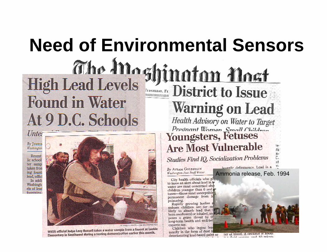
Need of Environmental Sensors
Ammonia release, Feb. 1994
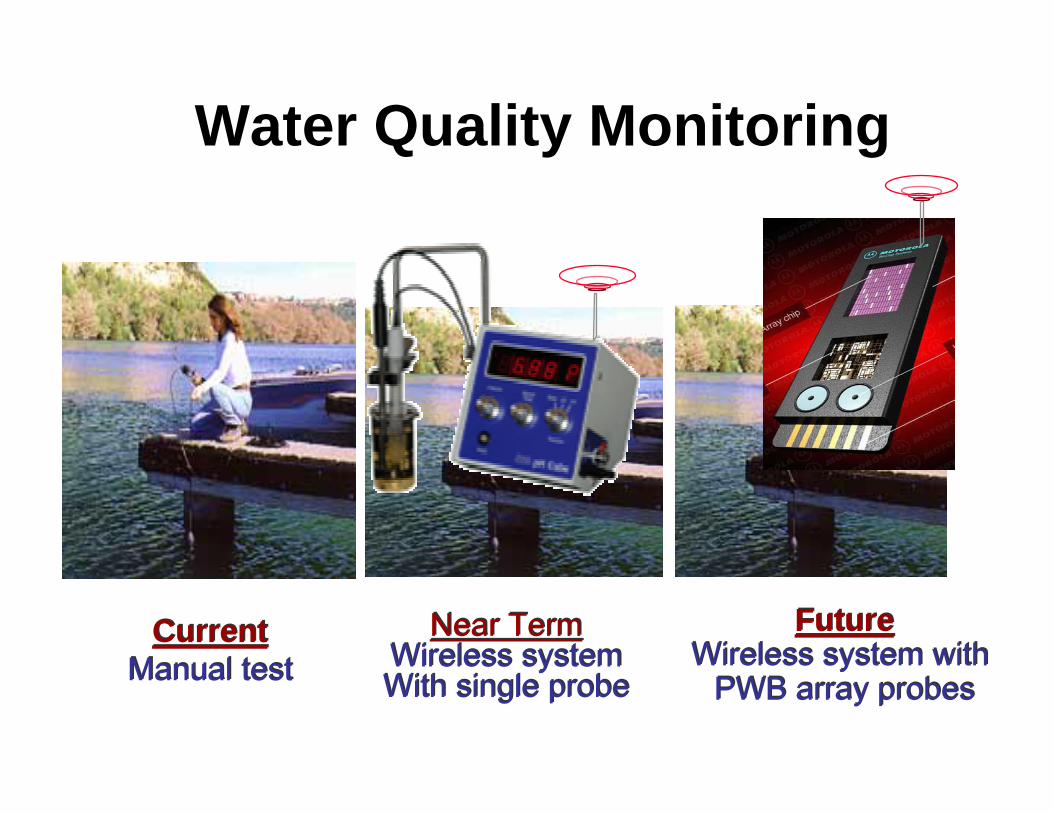
Water Quality Monitoring
CurrentManual test
CurrentManual test
Near TermWireless systemWith single probe
Near TermWireless systemWith single probe
FutureWireless system with
PWB array probes
FutureWireless system with
PWB array probes

Air Quality Monitoring
CurrentOnly select personnel
(Hazmat) typically carry portable equipment
Near TermProvide wireless connectivity of
portable equipment to communicate to incident commander
FutureEssential monitoring is
integrated into communications equipment
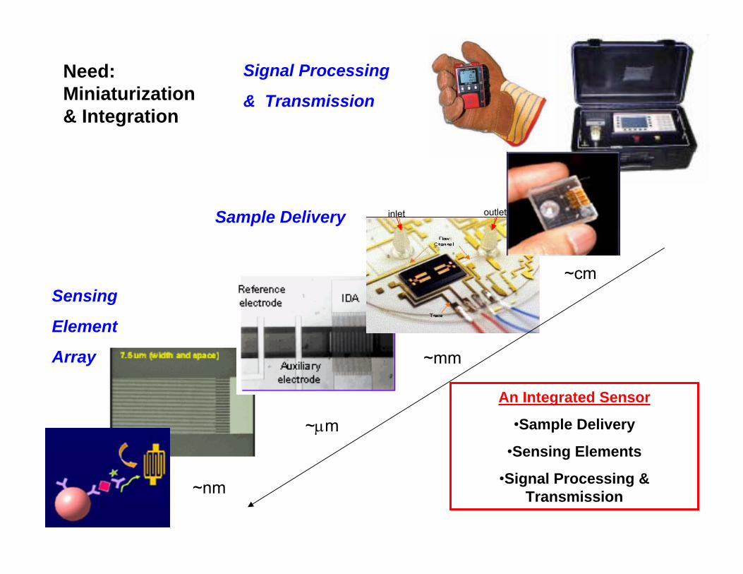
Need: Miniaturization & Integration
An Integrated Sensor
•Sample Delivery
•Sensing Elements
•Signal Processing & Transmission
Signal Processing
& Transmission
Sensing
Element
Array
Sample Delivery inlet outlet
~cm
~mm
~µm
~nm
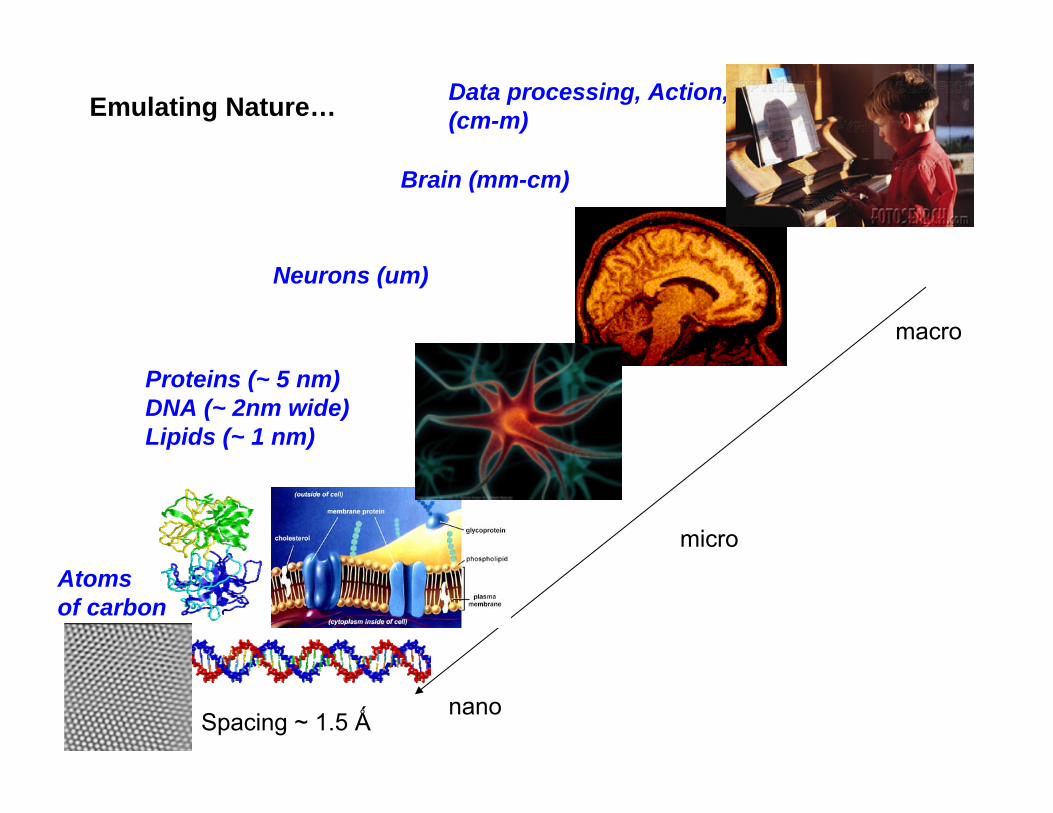
Neurons (um)
Proteins (~ 5 nm)DNA (~ 2nm wide)Lipids (~ 1 nm)
Atomsof carbon
Spacing ~ 1.5 Ǻ
Brain (mm-cm)
Data processing, Action,(cm-m)Emulating Nature…
macro
micro
nano
SignalProcessing
DataCommunication
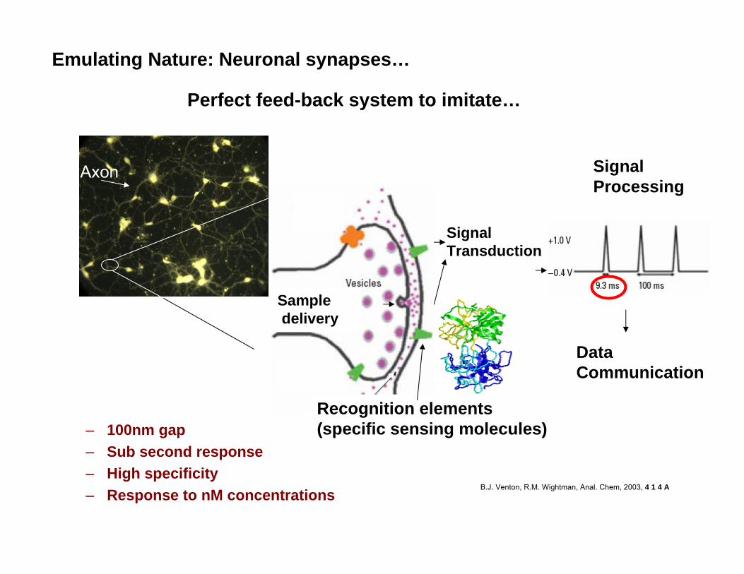
Emulating Nature: Neuronal synapses…
Perfect feed-back system to imitate…
– 100nm gap– Sub second response– High specificity– Response to nM concentrations
Analytes
Axon
SignalTransduction
Sampledelivery
Recognition elements(specific sensing molecules)
B.J. Venton, R.M. Wightman, Anal. Chem, 2003, 4 1 4 A
What role does ‘NANO’ play?
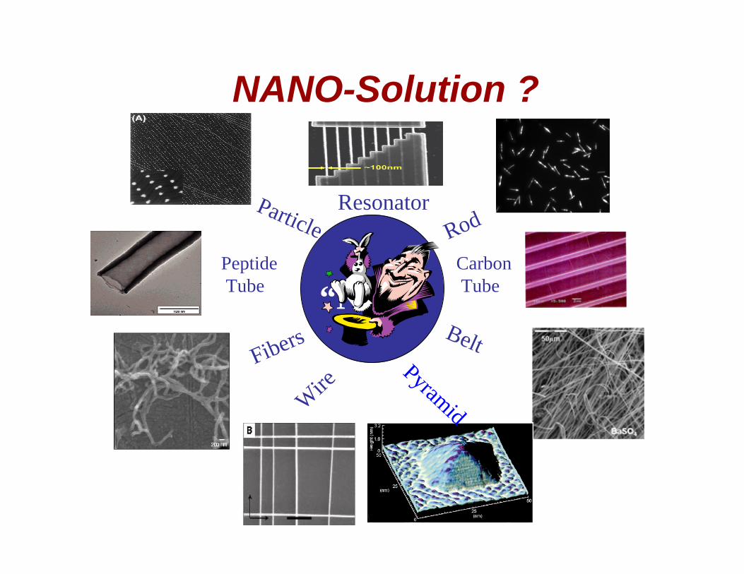
“Nano”
Rod
CarbonTube
Wire
Belt
ParticleResonator
PeptideTube
NANO-Solution ?
Pyramid
Fibers
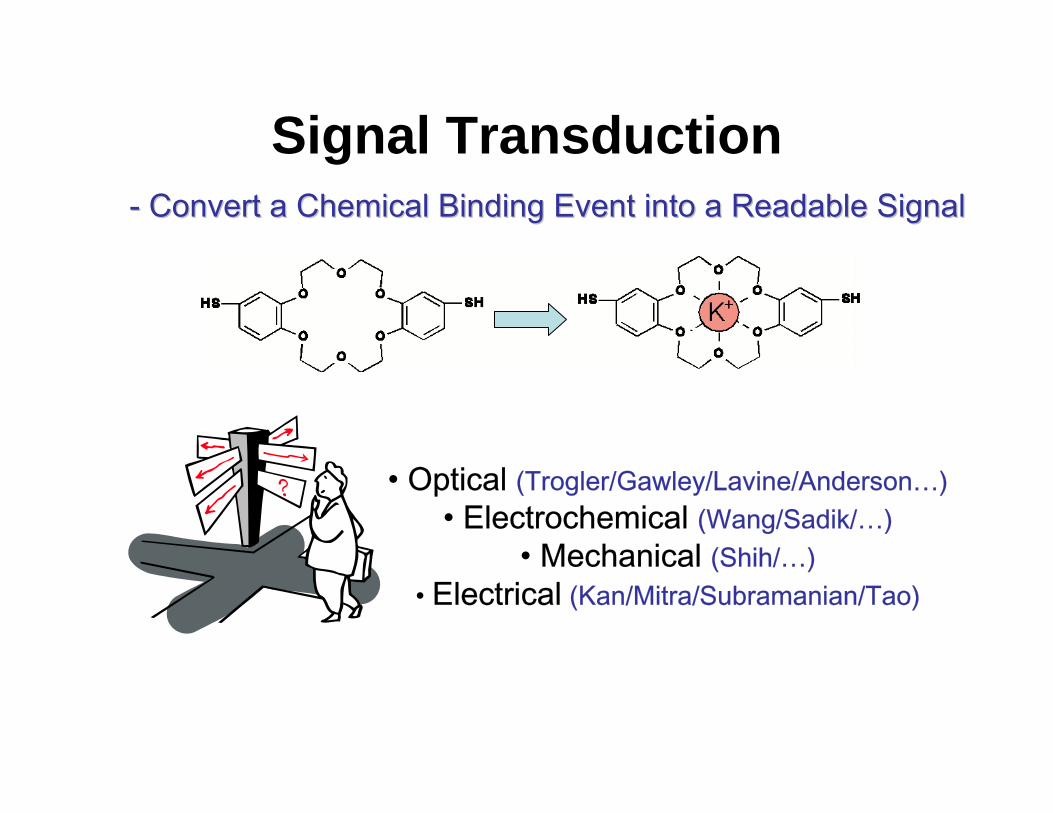
Signal Transduction-- Convert a Chemical Binding Event into a Readable SignalConvert a Chemical Binding Event into a Readable Signal
• Optical (Trogler/Gawley/Lavine/Anderson…)• Electrochemical (Wang/Sadik/…)
• Mechanical (Shih/…)• Electrical (Kan/Mitra/Subramanian/Tao)
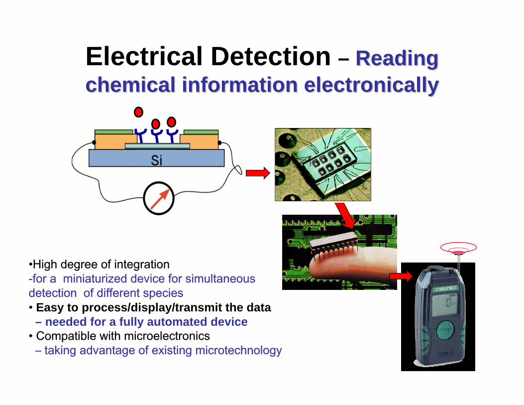
Electrical Detection – Reading Reading chemical information electronicallychemical information electronically
•High degree of integration -for a miniaturized device for simultaneous detection of different species• Easy to process/display/transmit the data – needed for a fully automated device
• Compatible with microelectronics – taking advantage of existing microtechnology
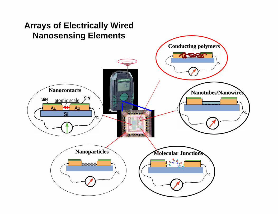
Arrays of Electrically Wired Nanosensing Elements
NanocontactsNanocontacts
atomic scaleNanotubes/NanowiresNanotubes/Nanowires
NanoparticlesNanoparticles Molecular JunctionsMolecular Junctions
Conducting polymersConducting polymers
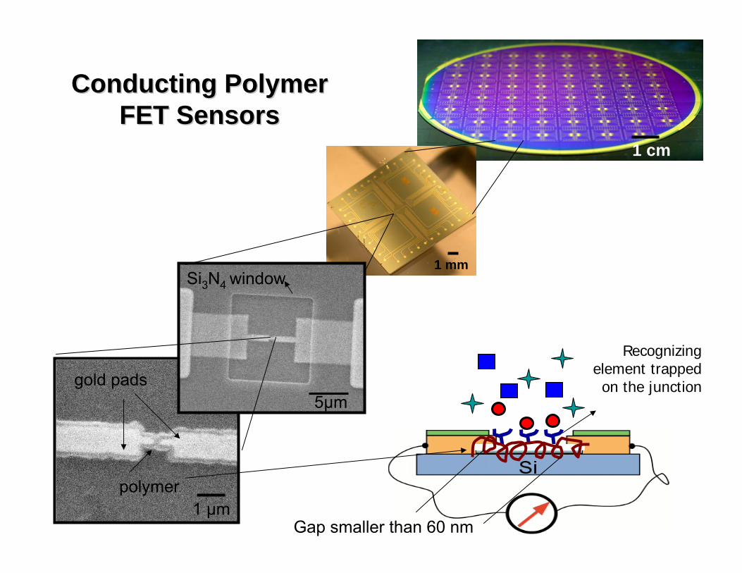
Recognizingelement trappedon the junction
Conducting Polymer Conducting Polymer FET SensorsFET Sensors
1 cm
1 mm
1 µmpolymer
gold pads
B
5µm
Si3N4 window
Gap smaller than 60 nm
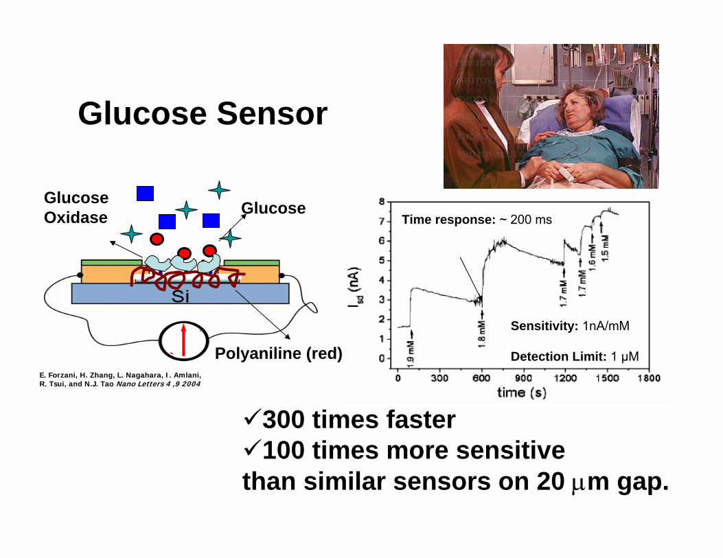
Glucose Sensor
E. Forzani, H. Zhang, L. Nagahara, I. Amlani,R. Tsui, and N.J. Tao Nano Letters 4 ,9 2004
300 times faster 100 times more sensitive
than similar sensors on 20 µm gap.
Time response: ~ 200 ms
Sensitivity: 1nA/mM
Detection Limit: 1 µM
GlucoseOxidase Glucose
Polyaniline (red)
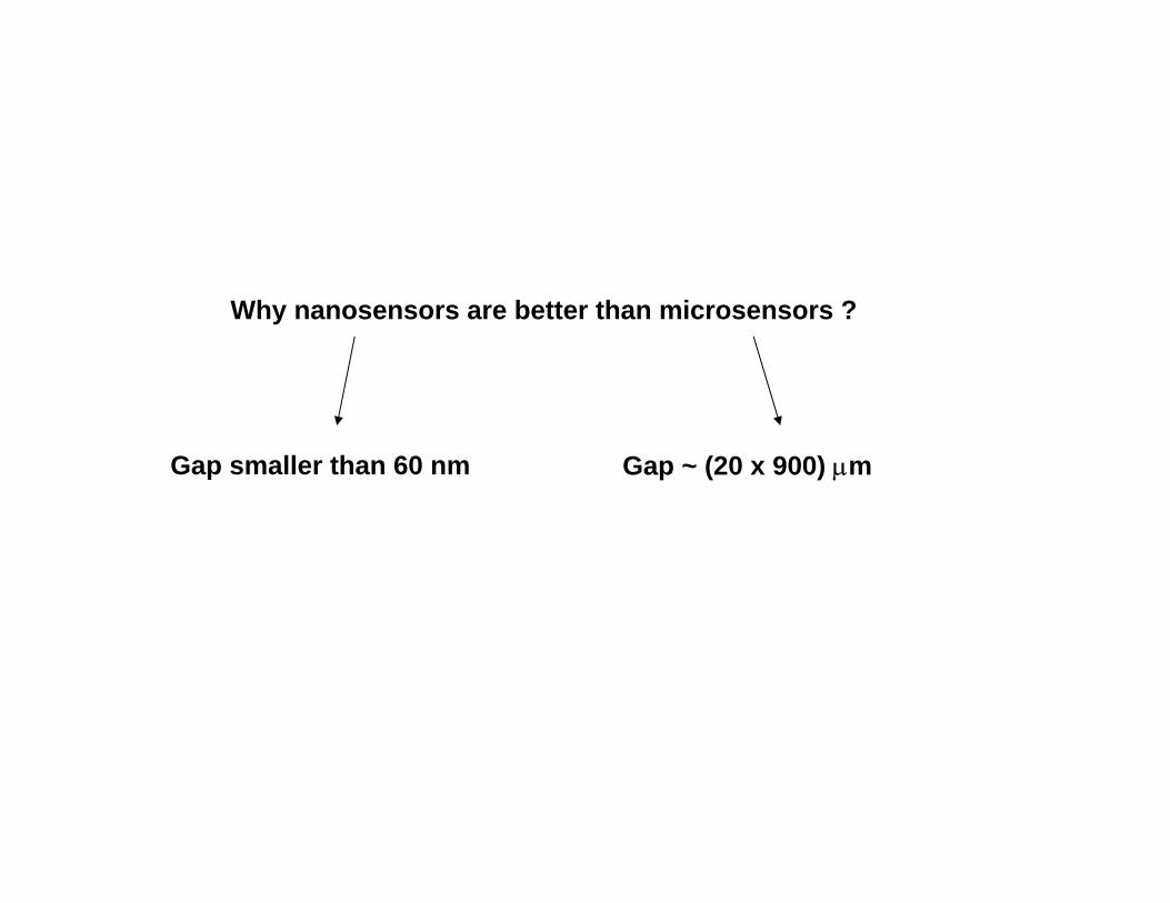
Why nanosensors are better than microsensors ?
Gap smaller than 60 nm Gap ~ (20 x 900) µm
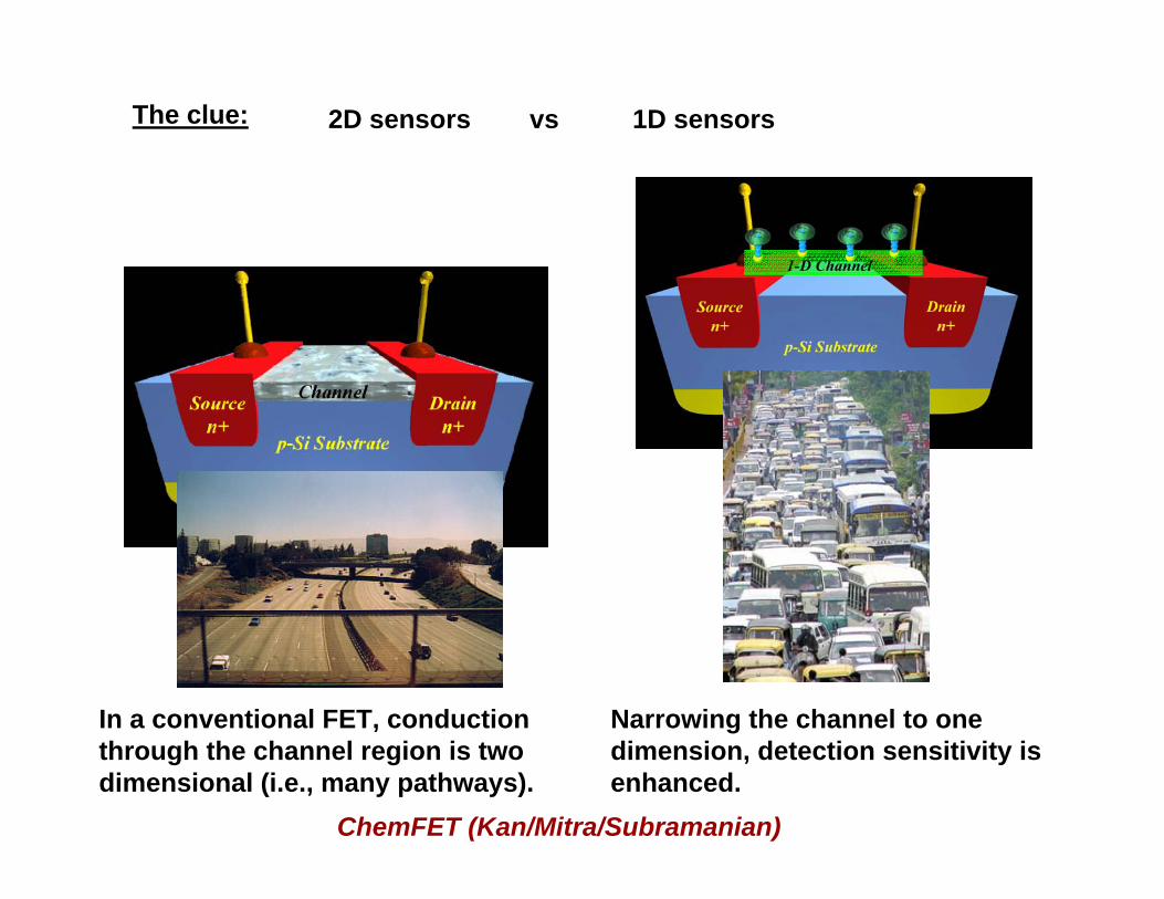
In a conventional FET, conduction through the channel region is two dimensional (i.e., many pathways).
Narrowing the channel to one dimension, detection sensitivity is enhanced.
ChemFET (Kan/Mitra/Subramanian)
The clue: 2D sensors vs 1D sensors

Is it necessary using real biological recognizing elements for environmental applications?

Peptides= peptidesMolecular Probe:
GlnApnGluAspArgLysHisCysMetThrSerTyr
tyrosPenProIleLeuValAlaGly
20 amino acids:
Building blocks of protein – Proteins in Nature as guidanceUnlimited Choices (4 amino acids ->20x20x20x20=160,000!)Powerful Combinatorial Chemistry
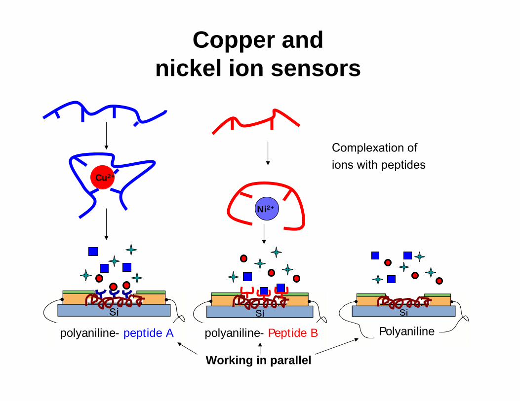
Copper and nickel ion sensors
Complexation of ions with peptides
polyaniline- Peptide B Polyaniline
Working in parallel
polyaniline- peptide A
Ni2+
Cu2+
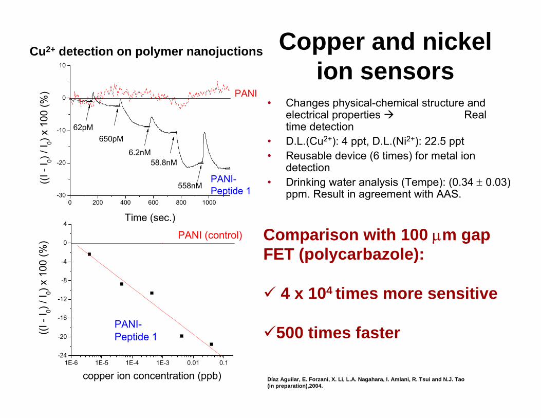
Copper and nickelion sensors
• Changes physical-chemical structure and electrical properties Real time detection
• D.L.(Cu2+): 4 ppt, D.L.(Ni2+): 22.5 ppt• Reusable device (6 times) for metal ion
detection• Drinking water analysis (Tempe): (0.34 ± 0.03)
ppm. Result in agreement with AAS.0 200 400 600 800 1000
-30
-20
-10
0
10
PANI-Peptide 1558nM
58.8nM6.2nM
650pM62pM
((I -
I 0) / I 0) x
100
(%)
Time (sec.)
PANI
Comparison with 100 µm gap FET (polycarbazole):
4 x 10⁴ times more sensitive
500 times faster
Cu2+ detection on polymer nanojuctions
1E-6 1E-5 1E-4 1E-3 0.01 0.1-24
-20
-16
-12
-8
-4
0
4
PANI (control)
((I -
I 0) / I 0) x
100
(%)
copper ion concentration (ppb)
PANI-Peptide 1
Díaz Aguilar, E. Forzani, X. Li, L.A. Nagahara, I. Amlani, R. Tsui and N.J. Tao(in preparation),2004.
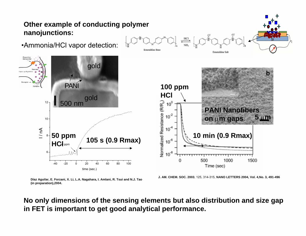
Other example of conducting polymer nanojunctions:
•Ammonia/HCl vapor detection:
-40 -20 0 20 40 60 80 100
6
8
10
12
50 ppm
PANI-PSS
time (sec.)
I / n
A
Díaz Aguilar, E. Forzani, X. Li, L.A. Nagahara, I. Amlani, R. Tsui and N.J. Tao(in preparation),2004.
J. AM. CHEM. SOC. 2003, 125, 314-315, NANO LETTERS 2004, Vol. 4,No. 3, 491-496
105 s (0.9 Rmax) 10 min (0.9 Rmax)
No only dimensions of the sensing elements but also distribution and size gapin FET is important to get good analytical performance.
50 ppmHCl
500 nm
PANI
gold
gold
5 µm
100 ppmHCl
PANI Nanofiberson µm gaps
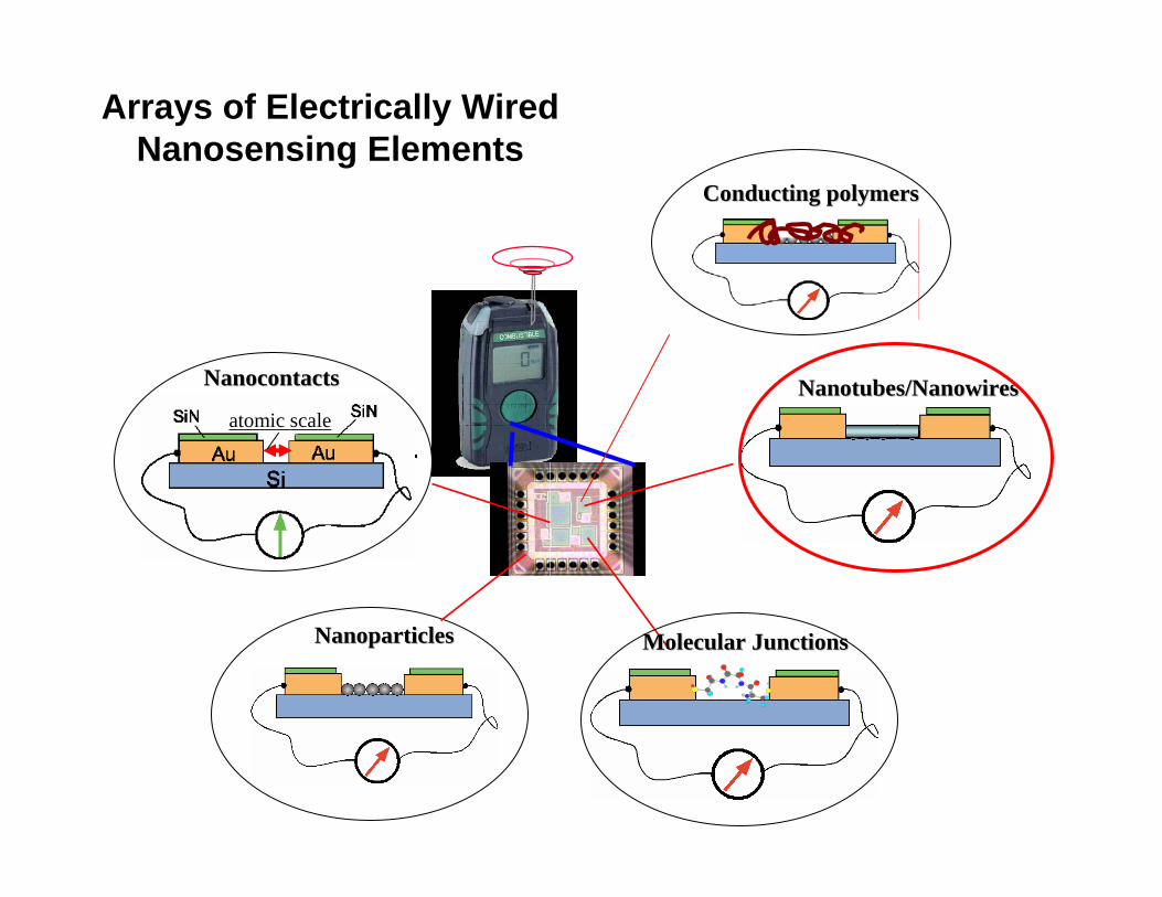
Arrays of Electrically Wired Nanosensing Elements
NanocontactsNanocontacts
atomic scaleNanotubes/NanowiresNanotubes/Nanowires
NanoparticlesNanoparticles Molecular JunctionsMolecular Junctions
Conducting polymersConducting polymers
NanotubesNanotubes//wireswires//beltsbelts SensorsSensors
NanotubesNanotubes NanowiresNanowires
R.M. Penner and co-workers(http://www.chem.uci.edu/people/faculty/rmpenner/)
NanobeltsNanobelts
R.J. Hamers & co-workers(http://hamers.chem.wisc.edu/)
C.M. Lieber and co-workers (http://cmliris.harvard.edu/)
H.J. Dai and co-workers(http://www.stanford.edu/dept/chemistry/faculty/dai/group/hongjie.html)
Z.L. Wang and co-workers(http://www.nanoscience.gatech.edu/zlwang/Research.htm)
N.V. Myung & co-worker + collaboratorshttp://www.engr.ucr.edu/~myung/Research.htm
ChongwuZhou & co-workers,http://ee.usc.edu/faculty_staff/bios/zhou.html

Carbon Carbon NanotubeNanotube FET SensorsFET Sensors
•Kong, J.; et al. Science 2000, 287, 622. •Zhou, C.; Kong, J.; Dai, H. Appl. Phys. Lett. 2000, 76, 1597. •Collins, P. G.; Bradley, K.; Ishigami, M.; Zettl, A. Science 2000, 287, 1801. •Hassanien et al., Appl. Phys. Lett., Vol. 79, No. 25, 17 December 2001
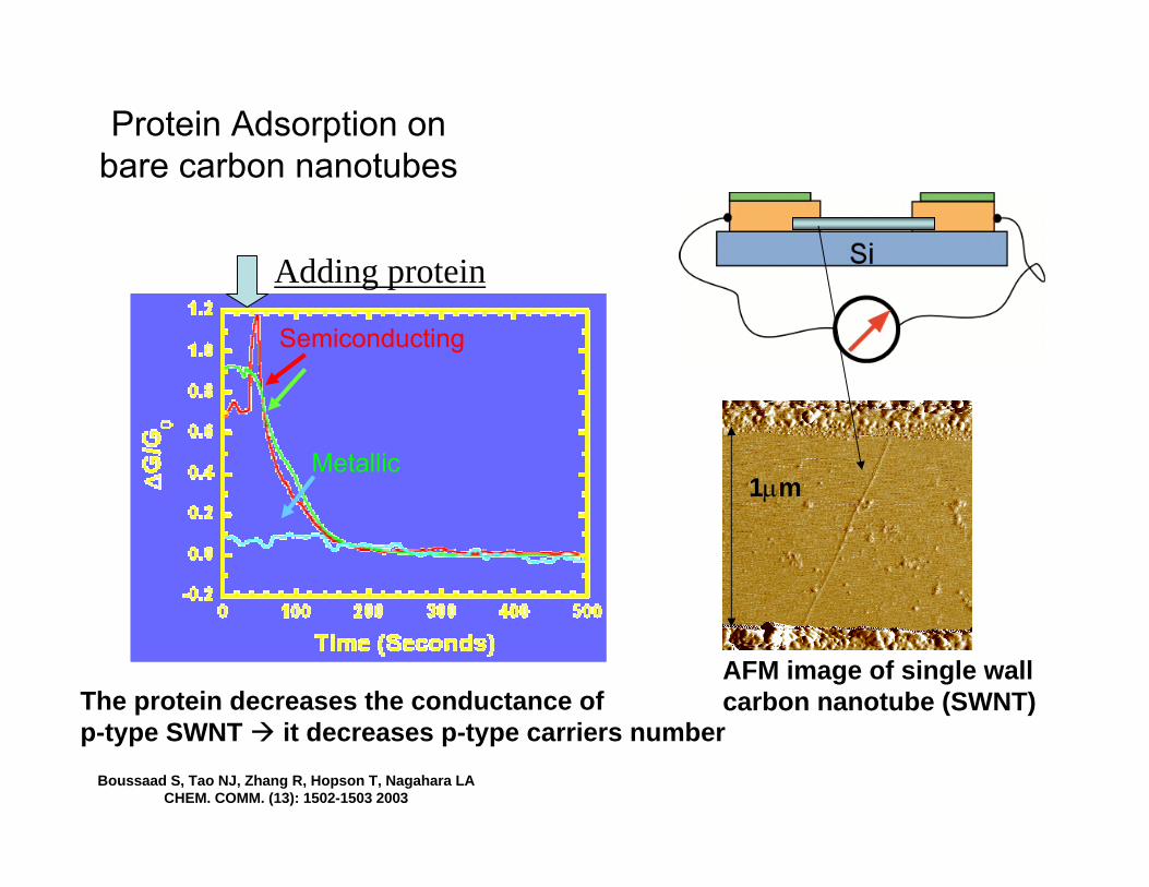
Protein Adsorption on bare carbon nanotubes
Semiconducting
Metallic
Adding protein
AFM image of single wallcarbon nanotube (SWNT)
Boussaad S, Tao NJ, Zhang R, Hopson T, Nagahara LA CHEM. COMM. (13): 1502-1503 2003
1µm
The protein decreases the conductance ofp-type SWNT it decreases p-type carriers number
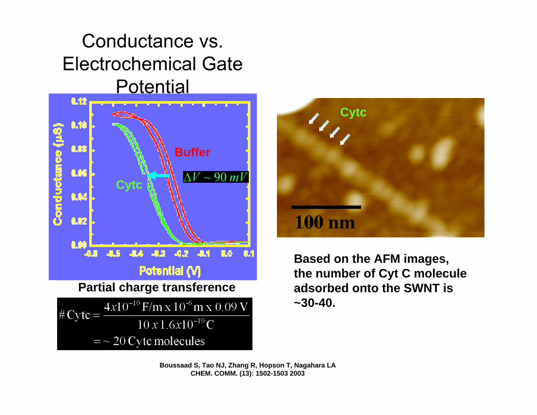
Conductance vs. Electrochemical Gate
Potential
Buffer
Cytc
Boussaad S, Tao NJ, Zhang R, Hopson T, Nagahara LA CHEM. COMM. (13): 1502-1503 2003
Partial charge transference
Cytc
Based on the AFM images, the number of Cyt C molecule adsorbed onto the SWNT is ~30-40.
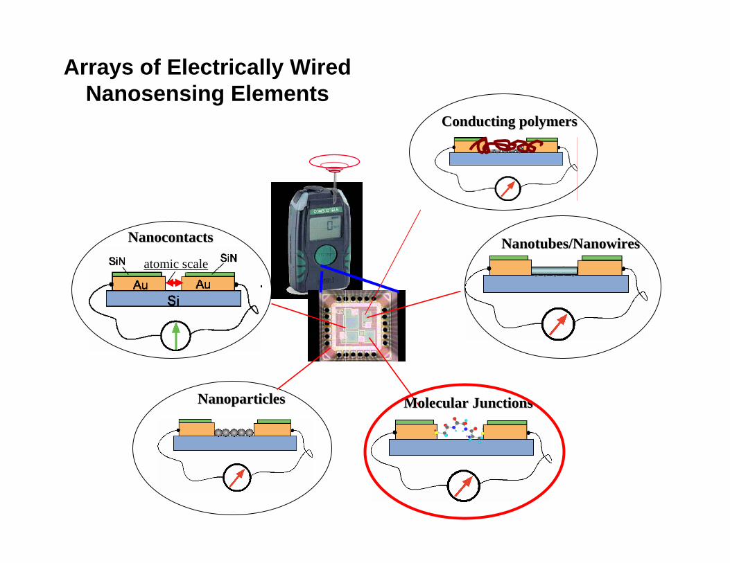
Arrays of Electrically Wired Nanosensing Elements
NanocontactsNanocontacts
atomic scaleNanotubes/NanowiresNanotubes/Nanowires
NanoparticlesNanoparticles Molecular JunctionsMolecular Junctions
Conducting polymersConducting polymers
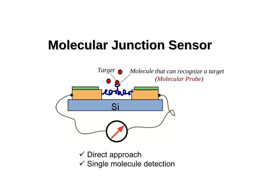
Molecular Junction SensorMolecular Junction Sensor
Target Molecule that can recognize a target(Molecular Probe)
Direct approachSingle molecule detection
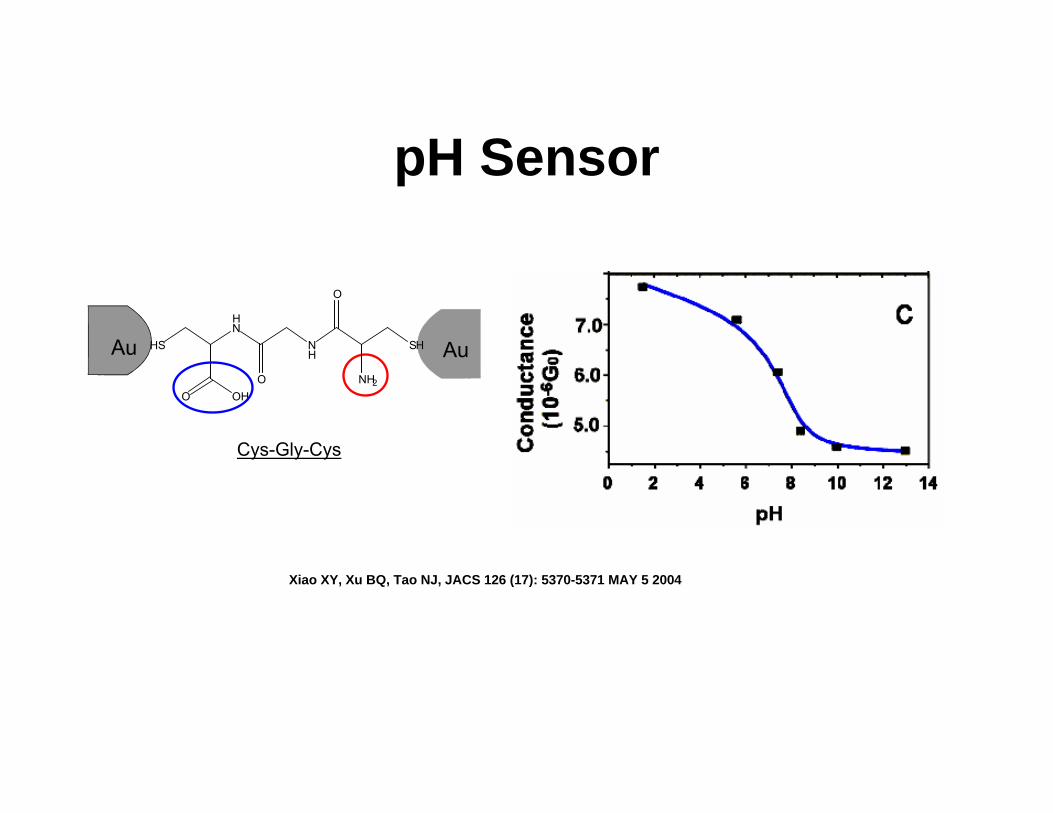
pH Sensor
Cys-Gly-Cys
Au AuNH2
O
SH
HN
OHO
HS NH
O
Xiao XY, Xu BQ, Tao NJ, JACS 126 (17): 5370-5371 MAY 5 2004
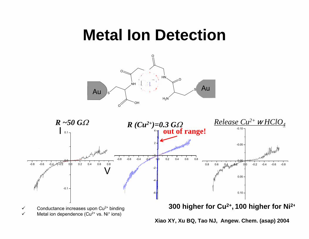
Metal Ion Detection
Au AuH2N
O
S
NH
OHO
S
HN
O
NH
O
R ~50 GΩ
-0.8 -0.6 -0.4 -0.2 0.0 0.2 0.4 0.6 0.8
-0.1
0.0
0.1
peptide 4
19 pA/V
I
V
out of range!
Cu2+
-0.8 -0.6 -0.4 -0.2 0.0 0.2 0.4 0.6 0.8
-6
-4
-2
0
2
4R (Cu2+)=0.3 GΩ
0.8 0.6 0.4 0.2 0.0 -0.2 -0.4 -0.6 -0.8
0.10
0.05
0.00
-0.05
-0.10
Release Cu2+ w HClO4
Conductance increases upon Cu2+ bindingMetal ion dependence (Cu2+ vs. Ni+ ions)
Xiao XY, Xu BQ, Tao NJ, Angew. Chem. (asap) 2004
300 higher for Cu2+, 100 higher for Ni2+
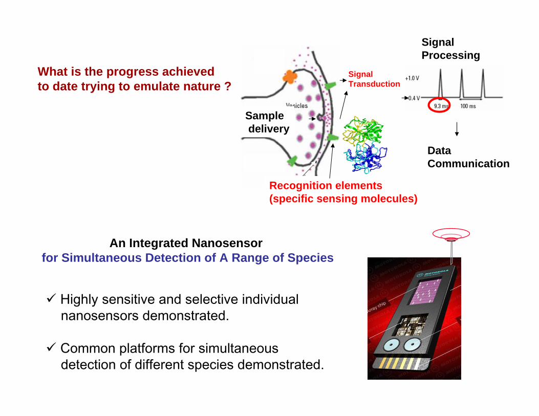
Highly sensitive and selective individual nanosensors demonstrated.
Common platforms for simultaneous detection of different species demonstrated.
An Integrated Nanosensorfor Simultaneous Detection of A Range of Species
SignalProcessing
DataCommunication
SignalTransduction
Sampledelivery
Recognition elements(specific sensing molecules)
What is the progress achieved to date trying to emulate nature ?
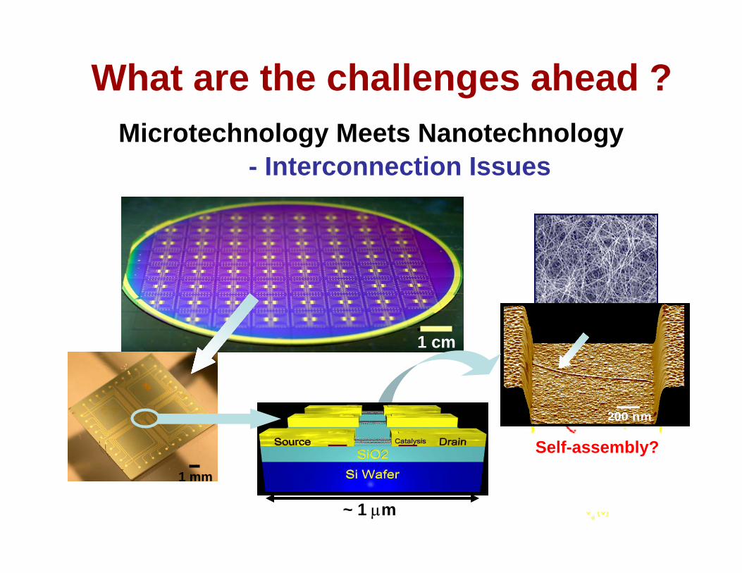
Microtechnology Meets Nanotechnology
1 cm
1 mm
SWNT(~2 nm)
~ 1 µm
- Interconnection Issues
What are the challenges ahead ?
Self-assembly?

Microtechnology Meets Nanotechnology
12
34 µm
1 mm
1 cm
- Sample Delivery
Challenges Ahead
Microfluidic Device
“Nano”
Rod
CarbonTube
WireBelt
ParticleResonator
PeptideTube
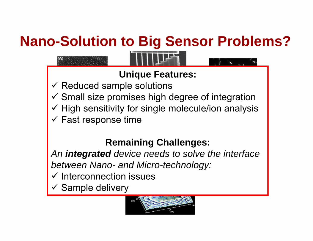
Nano-Solution to Big Sensor Problems?
Pyramid
Unique Features:Reduced sample solutionsSmall size promises high degree of integrationHigh sensitivity for single molecule/ion analysisFast response time
Remaining Challenges:An integrated device needs to solve the interface between Nano- and Micro-technology:
Interconnection issuesSample delivery
AcknowledgementsAcknowledgements
• Nongjian Tao• Al Diaz• Xiulan Li• Bingqian Xu• Xiaoyin Xiao• John Zhang (Nanjing University)• Salah Boussaad (Dupont)
• Larry Nagahara• Islamshah Almani• Ruth Zhang• Ray Tsui