nanotechnology and you - d'trends · nanotechnology and you john werry ... • nanoscience is...
TRANSCRIPT
Nanotechnology and you
John WerryDept of Innovation, Industry and
Regional Development

Teaching emerging sciencesCommon Questions:• How does it fit the syllabus I am meant to
teach?• If these are so high-tech, how can I do hands
on activities with my students?• How can I teach this when I don’t understand
it anyway?
Two case studies
• Nanotechnology
• Synchrotron Science
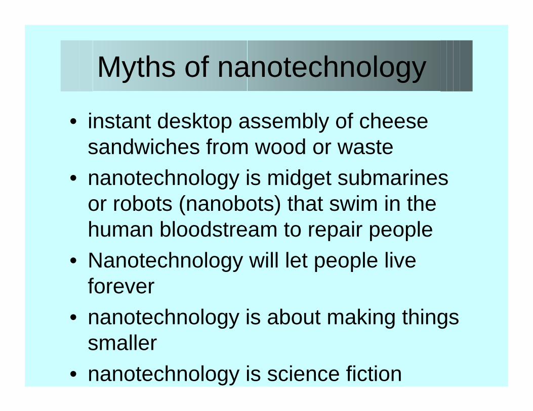
Myths of nanotechnology
• instant desktop assembly of cheesesandwiches from wood or waste
• nanotechnology is midget submarinesor robots (nanobots) that swim in thehuman bloodstream to repair people
• Nanotechnology will let people liveforever
• nanotechnology is about making thingssmaller
• nanotechnology is science fiction
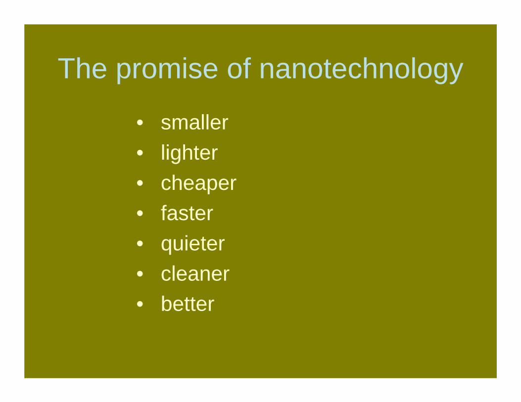
The promise of nanotechnology
• smaller• lighter• cheaper• faster• quieter• cleaner• better
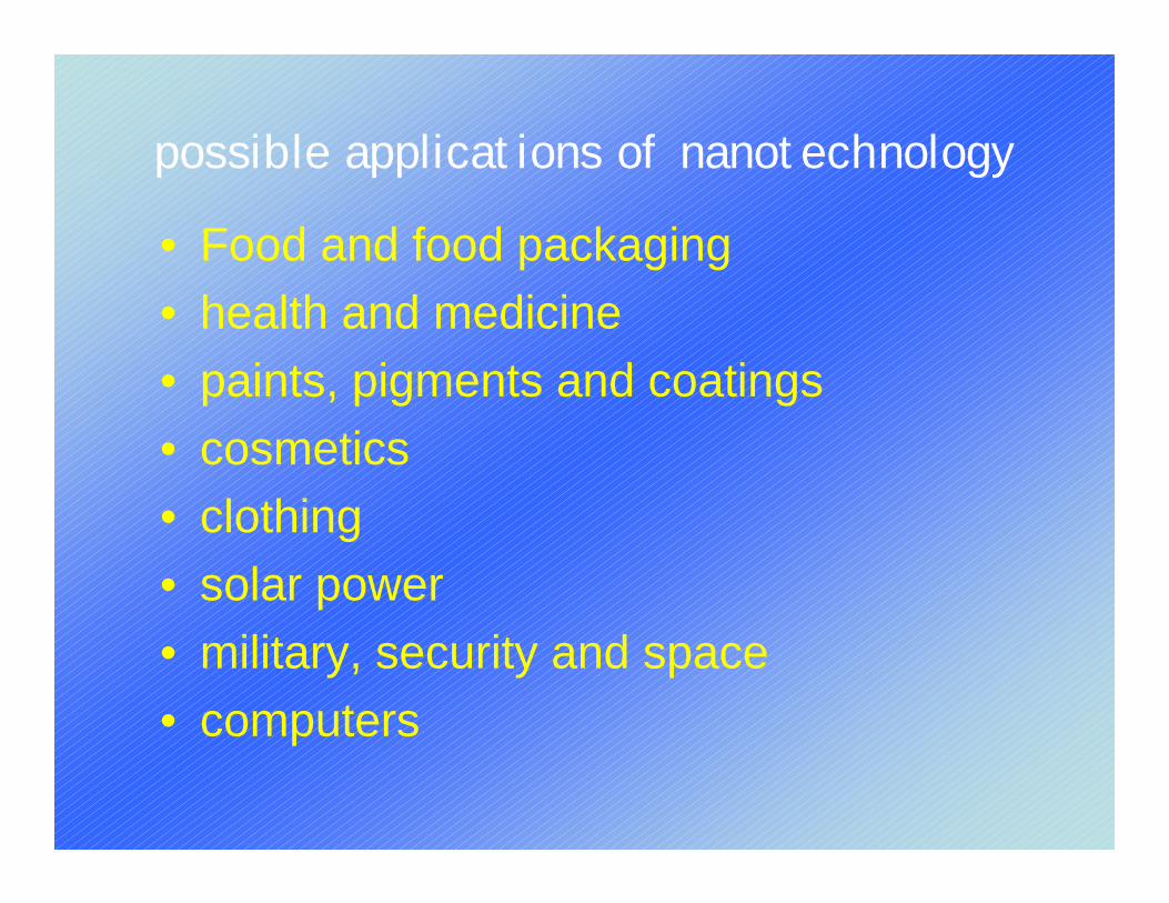
possible applications of nanotechnology
• Food and food packaging• health and medicine• paints, pigments and coatings• cosmetics• clothing• solar power• military, security and space• computers
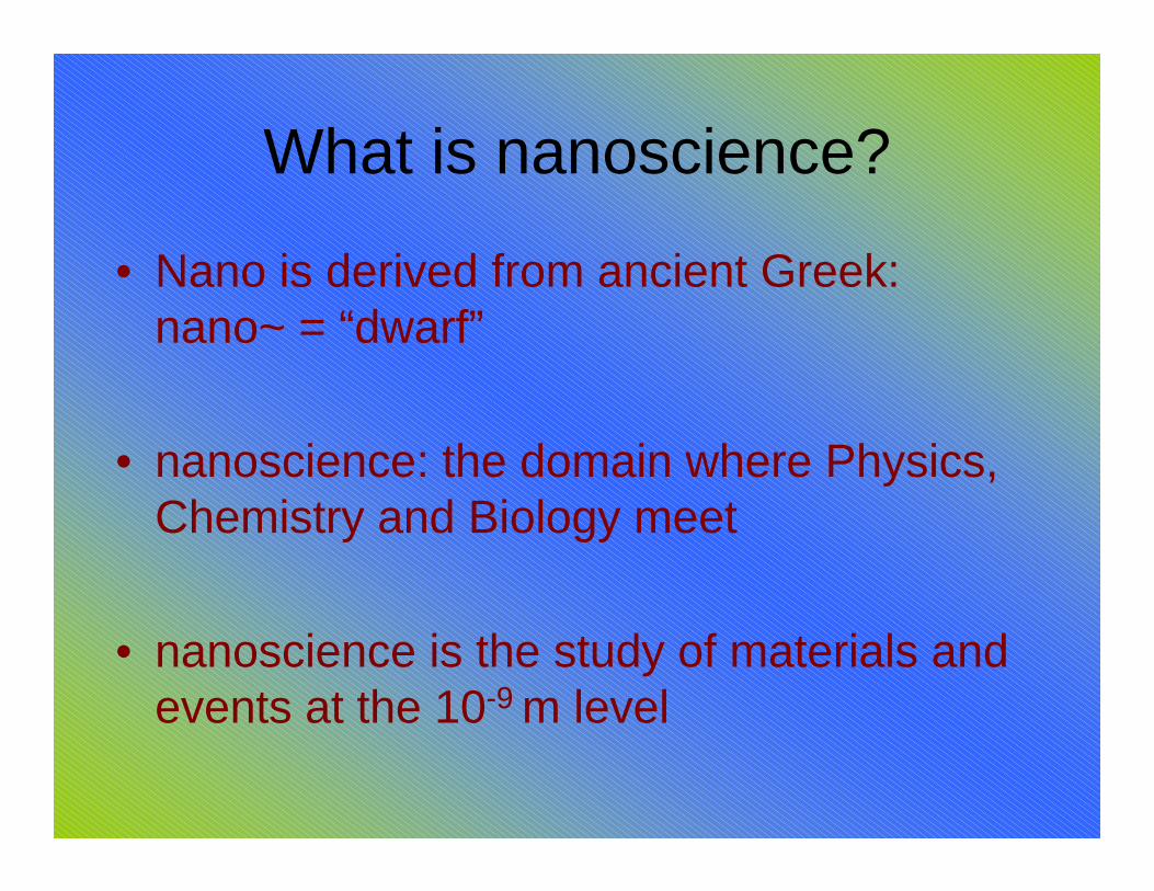
What is nanoscience?
• Nano is derived from ancient Greek:nano~ = “dwarf”
• nanoscience: the domain where Physics,Chemistry and Biology meet
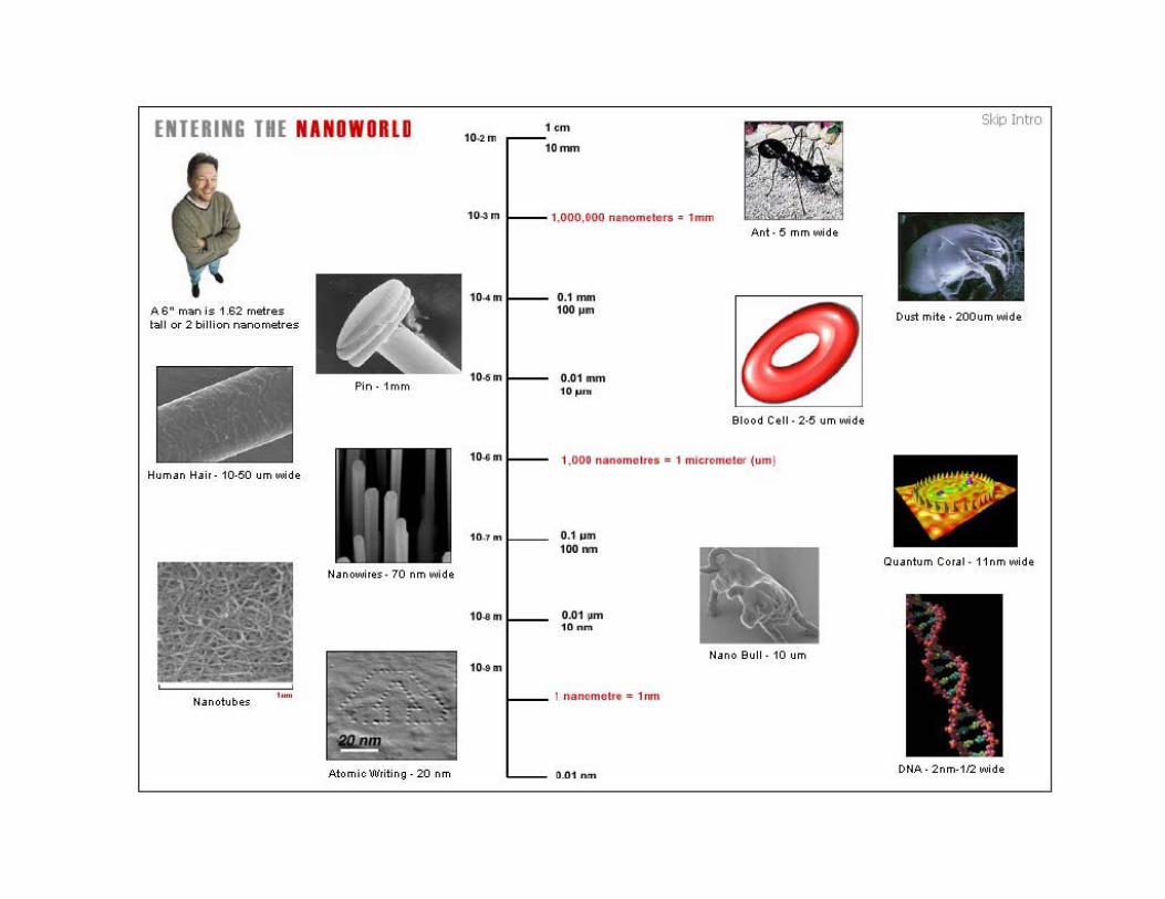
• nanoscience is the study of materials andevents at the 10-9 m level
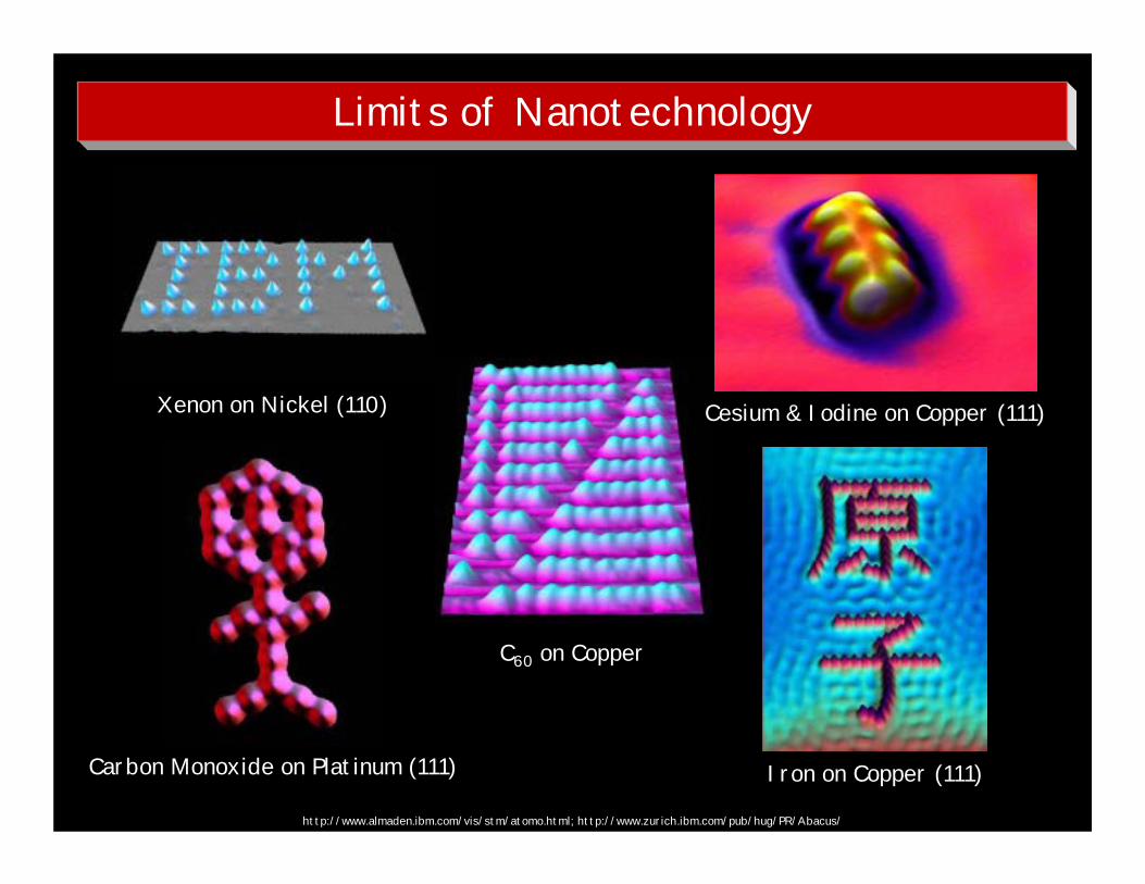
Carbon Monoxide on Platinum (111)
Xenon on Nickel (110)
http://www.almaden.ibm.com/vis/stm/atomo.html; http://www.zurich.ibm.com/pub/hug/PR/Abacus/
Limits of Nanotechnology
Cesium & Iodine on Copper (111)
Iron on Copper (111)
C60 on Copper
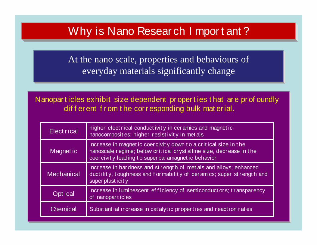
At the nano scale, properties and behaviours ofeveryday materials significantly change
Why is Nano Research Important?
Substantial increase in catalytic properties and reaction ratesChemical
increase in luminescent efficiency of semiconductors; transparencyof nanoparticlesOptical
increase in hardness and strength of metals and alloys; enhancedductility, toughness and formability of ceramics; super strength andsuperplasticity
Mechanical
increase in magnetic coercivity down to a critical size in thenanoscale regime; below critical crystalline size, decrease in thecoercivity leading to superparamagnetic behavior
Magnetic
higher electrical conductivity in ceramics and magneticnanocomposites; higher resistivity in metalsElectrical
Nanoparticles exhibit size dependent properties that are profoundly different from the corresponding bulk material.
History of nanotechnology
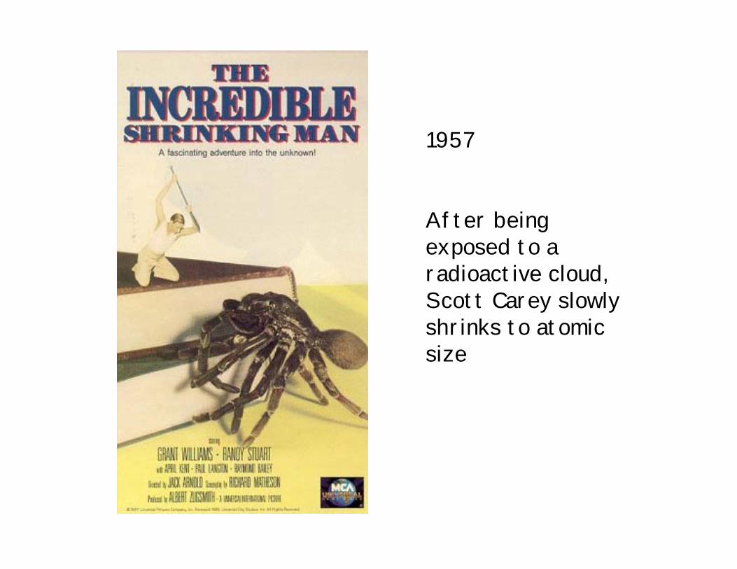
1957
After beingexposed to aradioactive cloud,Scott Carey slowlyshrinks to atomicsize
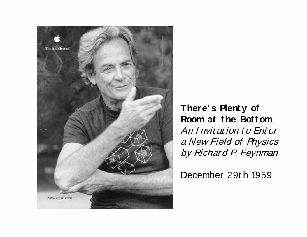
There's Plenty ofRoom at the BottomAn Invitation to Entera New Field of Physicsby Richard P. Feynman
December 29th 1959
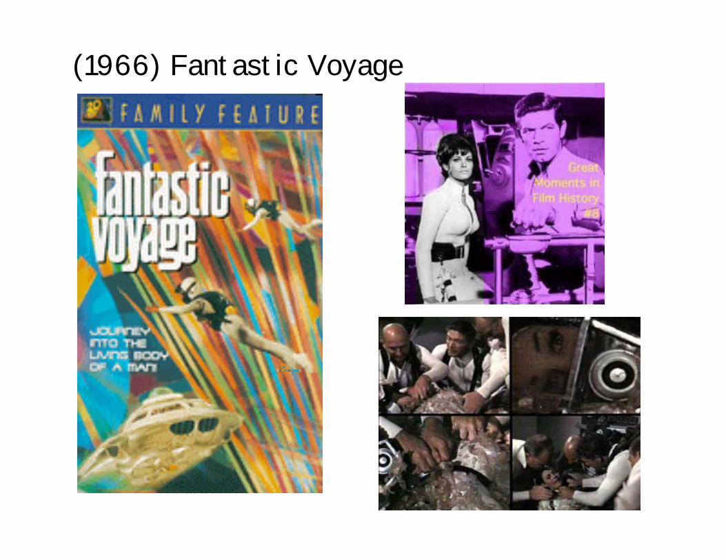
(1966) Fantastic Voyage
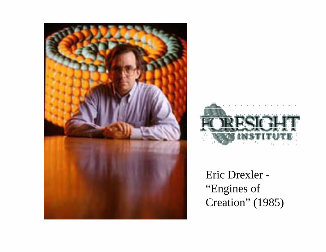
Eric Drexler -“Engines ofCreation” (1985)
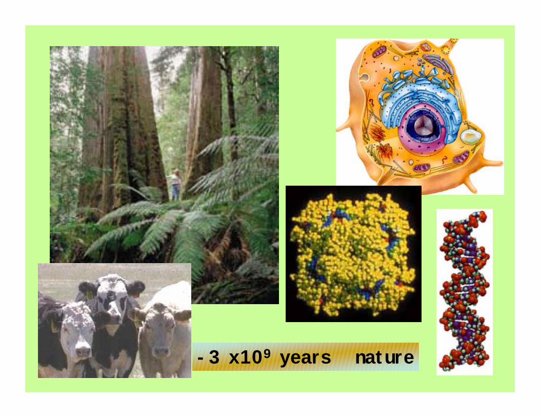
-3 x10⁹ years nature
What is nanotechnology?
Many things to many people but twoaspects are common:
• Creation of “new” materials and devicesfrom being able to manipulateproperties at the level of atoms.
• Exploitation of strange and newproperties of materials of less than 100nm - such as nanopowders and nano-crystals.
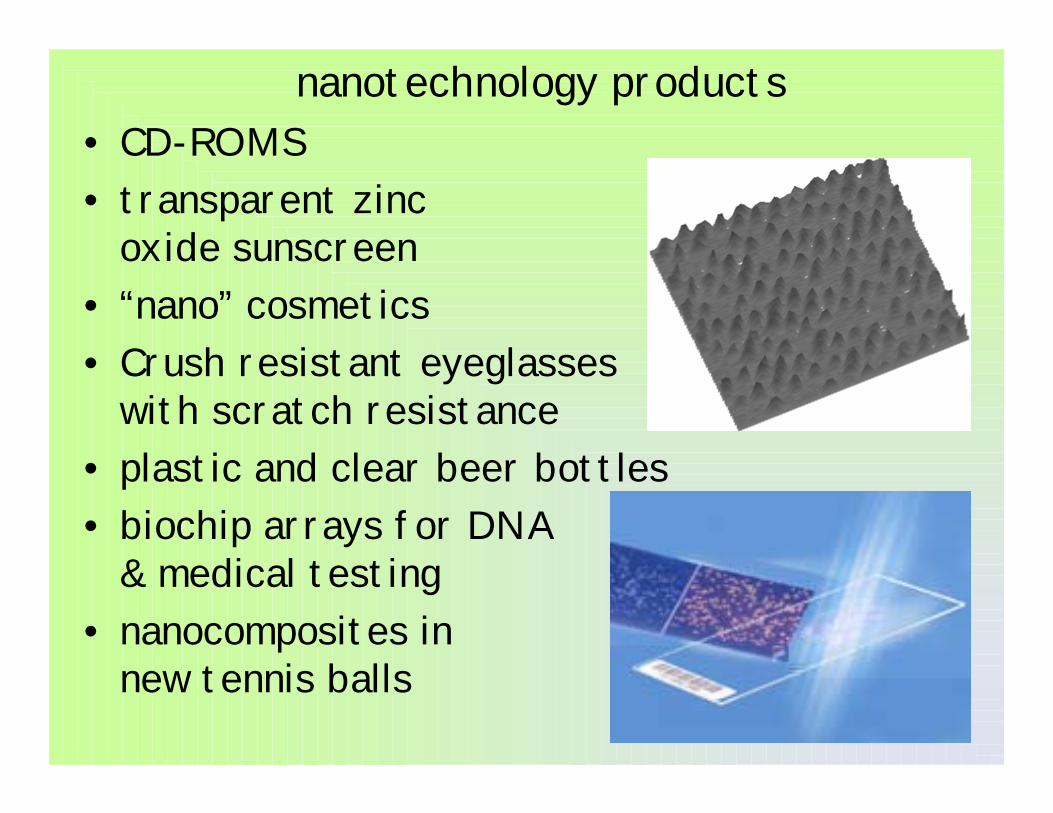
nanotechnology products• CD-ROMS• transparent zinc
oxide sunscreen• “nano” cosmetics• Crush resistant eyeglasses
with scratch resistance• plastic and clear beer bottles• biochip arrays for DNA
& medical testing• nanocomposites in
new tennis balls
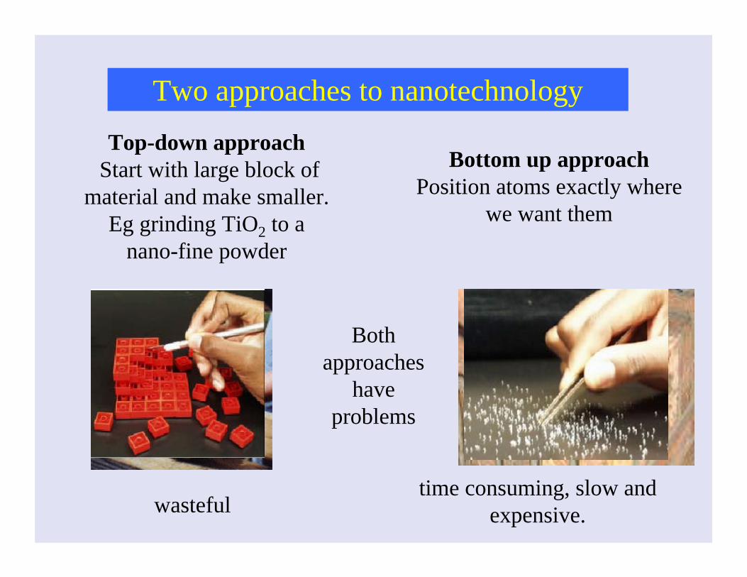
Two approaches to nanotechnologyTop-down approach
Start with large block ofmaterial and make smaller.
Eg grinding TiO2 to anano-fine powder
Bottom up approachPosition atoms exactly where
we want them
Bothapproaches
haveproblems
wastefultime consuming, slow and
expensive.
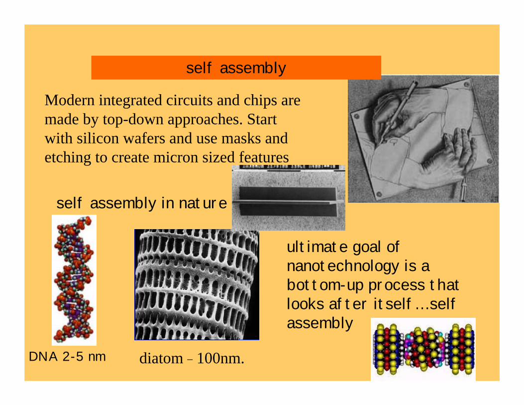
Modern integrated circuits and chips aremade by top-down approaches. Startwith silicon wafers and use masks andetching to create micron sized features
diatom _ 100nm.
self assembly
ultimate goal ofnanotechnology is abottom-up process thatlooks after itself… selfassembly
self assembly in nature
DNA 2-5 nm

PRODUCT CASE STUDIES
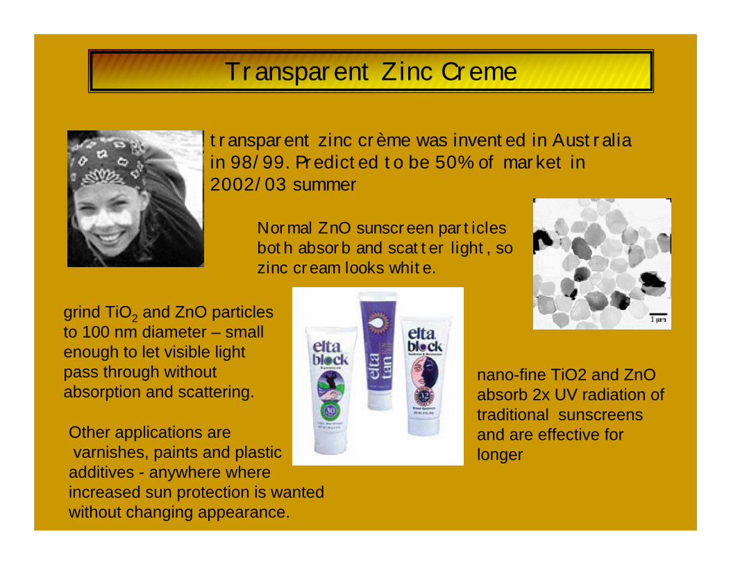
Transparent Zinc Creme
transparent zinc crème was invented in Australiain 98/99. Predicted to be 50% of market in2002/03 summer
Normal ZnO sunscreen particlesboth absorb and scatter light, sozinc cream looks white.
grind TiO2 and ZnO particlesto 100 nm diameter – smallenough to let visible lightpass through withoutabsorption and scattering.
nano-fine TiO2 and ZnOabsorb 2x UV radiation oftraditional sunscreensand are effective forlonger
Other applications are varnishes, paints and plasticadditives - anywhere whereincreased sun protection is wantedwithout changing appearance.
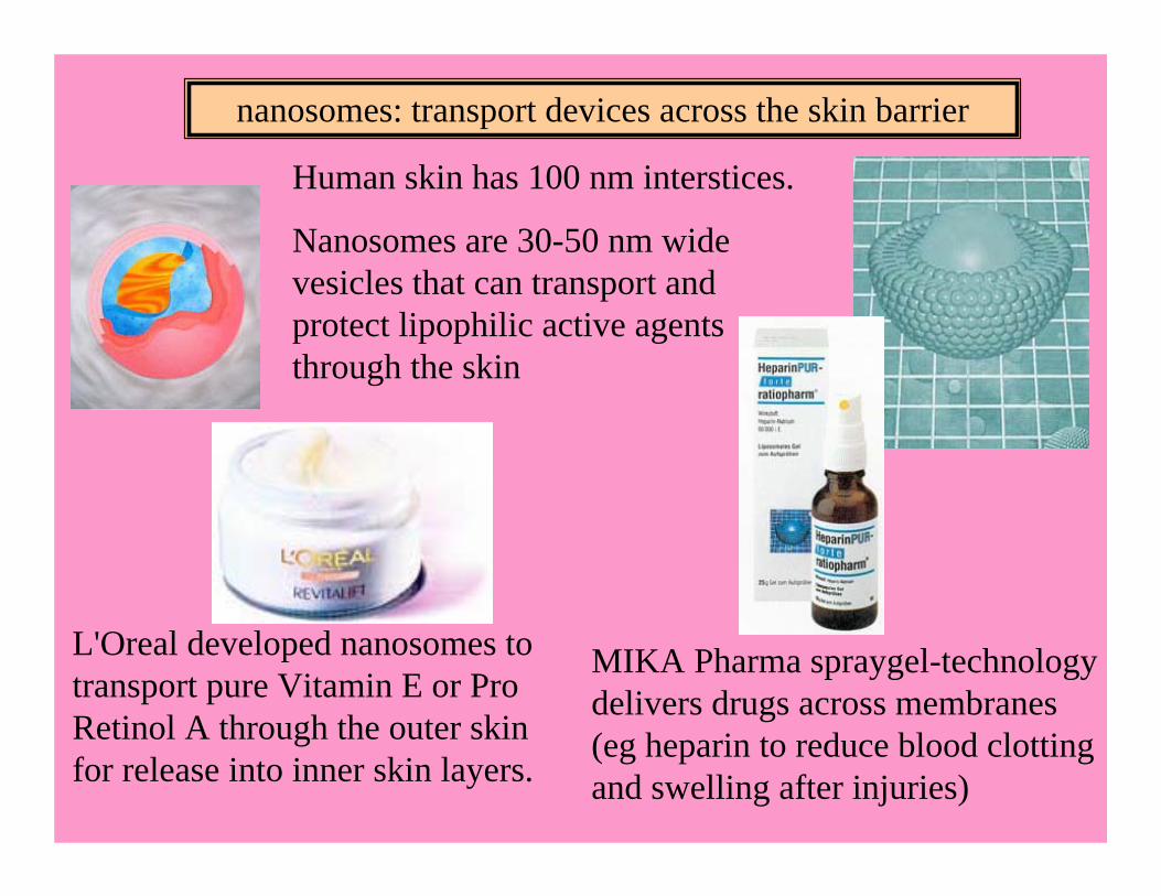
nanosomes: transport devices across the skin barrier
Human skin has 100 nm interstices.
Nanosomes are 30-50 nm widevesicles that can transport andprotect lipophilic active agentsthrough the skin
L'Oreal developed nanosomes totransport pure Vitamin E or ProRetinol A through the outer skinfor release into inner skin layers.
MIKA Pharma spraygel-technologydelivers drugs across membranes(eg heparin to reduce blood clottingand swelling after injuries)
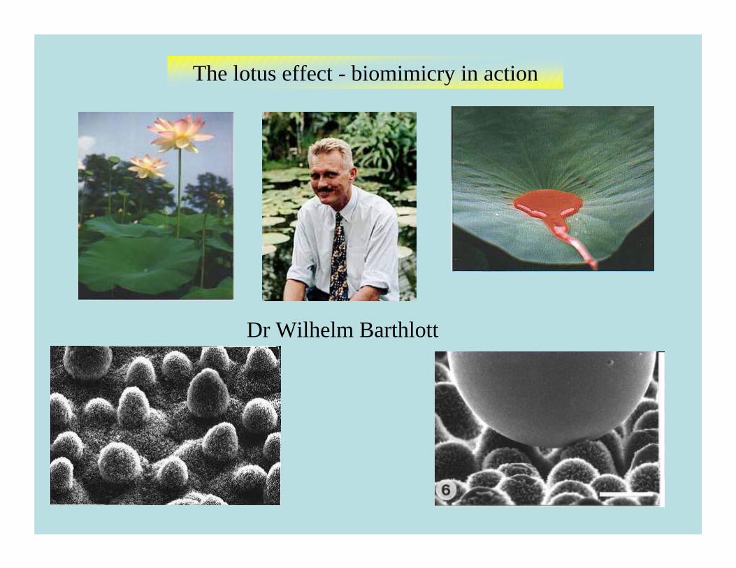
The lotus effect - biomimicry in action
Dr Wilhelm Barthlott
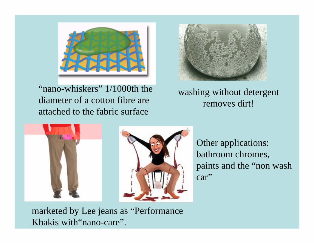
“nano-whiskers” 1/1000th thediameter of a cotton fibre areattached to the fabric surface
washing without detergentremoves dirt!
Other applications:bathroom chromes,paints and the “non washcar”
marketed by Lee jeans as “PerformanceKhakis with“nano-care”.
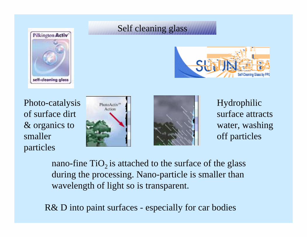
Self cleaning glass
nano-fine TiO2 is attached to the surface of the glassduring the processing. Nano-particle is smaller thanwavelength of light so is transparent.
Photo-catalysisof surface dirt& organics tosmallerparticles
Hydrophilicsurface attractswater, washingoff particles
R& D into paint surfaces - especially for car bodies

me
mo
ry
m
et
al
Li
nk
1
Ni
Ti
a
ll
oy
(
ni
to
l)
d
ev
el
op
ed
b
y
US
n
av
y
Ca
n
de
fo
rm
s
ha
pe
o
f
al
lo
y.
H
ea
t
in
w
ar
m
wa
te
ra
nd
a
ll
oy
r
et
ur
ns
t
o
or
ig
in
al
s
ha
pe
http://www.ipt.arc.nasa.gov/gallery.html; http://www.nano.com/an-pg-body.html
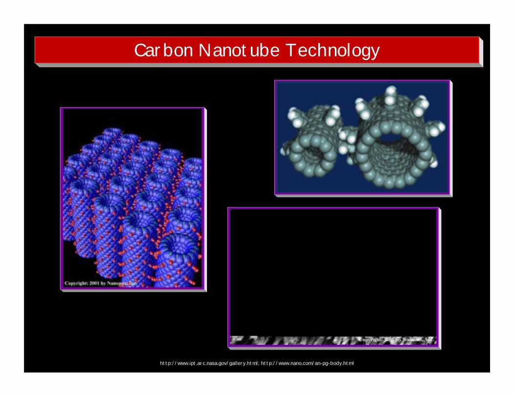
Carbon Nanotube Technology
Grace, L. in “Nanotubes for Electronics,” P. G. Collins and P. Avouris, Scientific American, 283(6), pp. 62 ff, Dec, 2000.
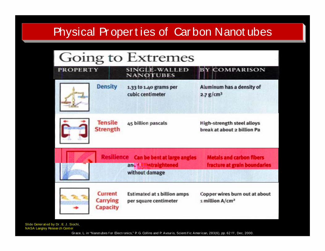
Physical Properties of Carbon Nanotubes
Slide Generated by Dr. E. J. Siochi, NASA Langley Research Center
Gibbs,W .W .in“Nanotubes forElectronics,”P.G.Collins and P.Avouris,ScientificAmerican,283(6),pp.62ff,Dec,2000.
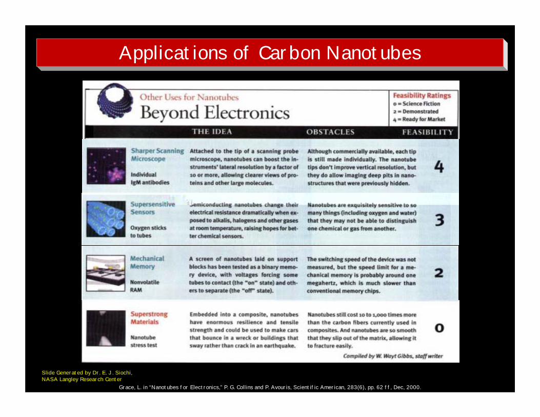
Applications of Carbon Nanotubes
Grace, L. in “Nanotubes for Electronics,” P. G. Collins and P. Avouris, Scientific American, 283(6), pp. 62 ff, Dec, 2000.
Slide Generated by Dr. E. J. Siochi, NASA Langley Research Center
Grace, L. in “Nanotubes for Electronics,” P. G. Collins and P. Avouris, Scientific American, 283(6), pp. 62 ff, Dec, 2000.
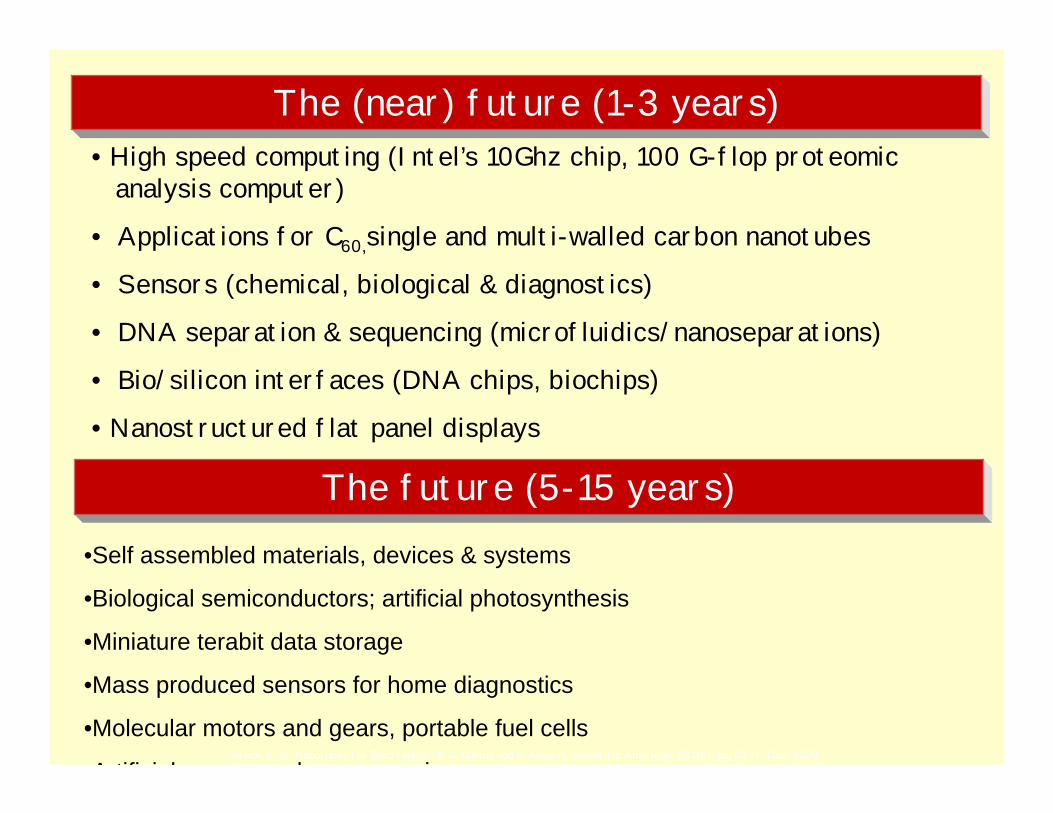
The (near) future (1-3 years)• High speed computing (Intel’s 10Ghz chip, 100 G-flop proteomic analysis computer)
• Applications for C60,single and multi-walled carbon nanotubes
• Sensors (chemical, biological & diagnostics)
• DNA separation & sequencing (microfluidics/nanoseparations)
• Bio/silicon interfaces (DNA chips, biochips)
• Nanostructured flat panel displays
The future (5-15 years)•Self assembled materials, devices & systems
•Biological semiconductors; artificial photosynthesis
•Miniature terabit data storage
•Mass produced sensors for home diagnostics
•Molecular motors and gears, portable fuel cells
A tifi i l d i

Social implications
Regardless of benefits …nanotechnology is a verydisruptive technology
Applications positive for consumer andcitizen – but not good for many existingoccupations
current developments threaten futurelivelihood of pathologists, dry
cleaners, textile workers, windowwashers, car washers, food handlers,
etc
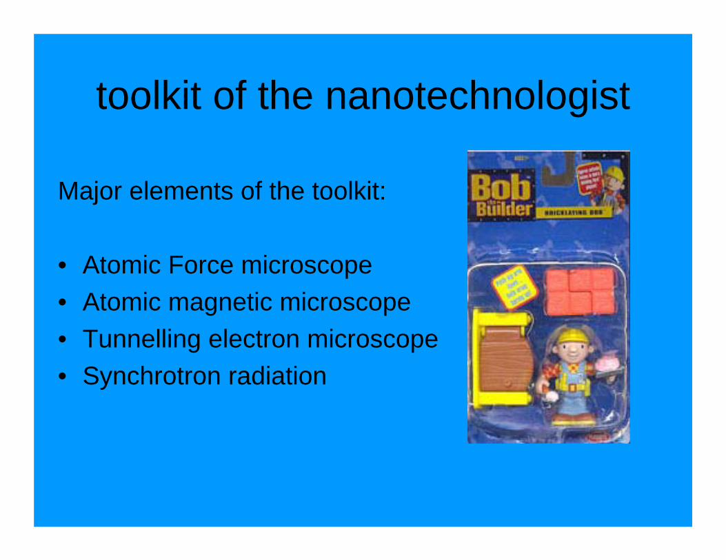
toolkit of the nanotechnologist
Major elements of the toolkit:
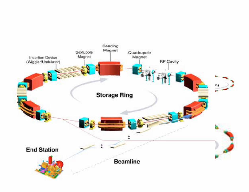
• Atomic Force microscope• Atomic magnetic microscope• Tunnelling electron microscope• Synchrotron radiation
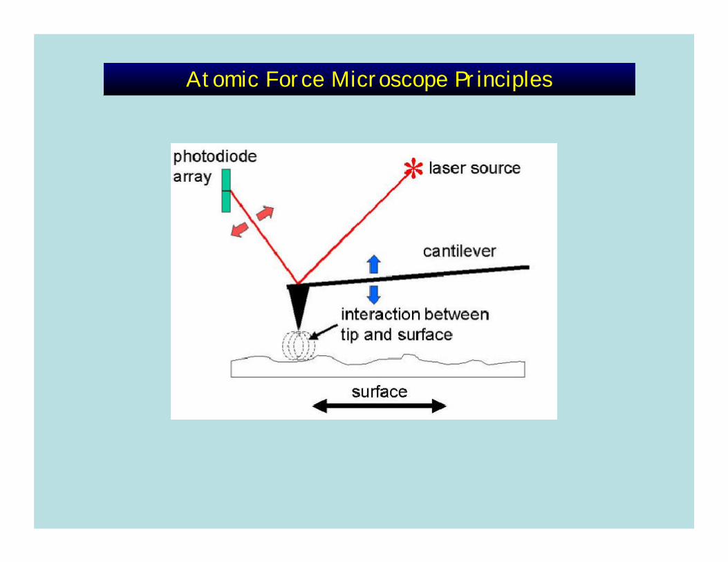
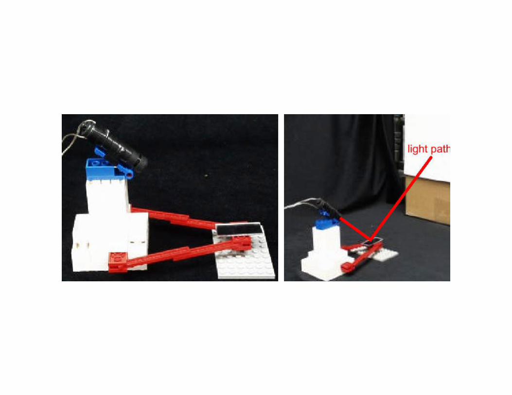
Atomic Force Microscope Principles
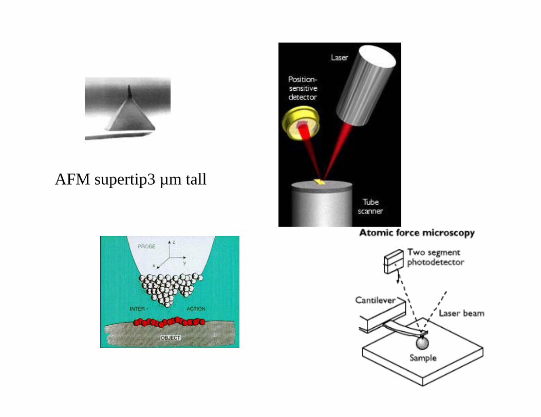
AFM supertip3 µm tall
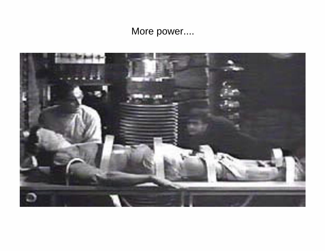
More power....
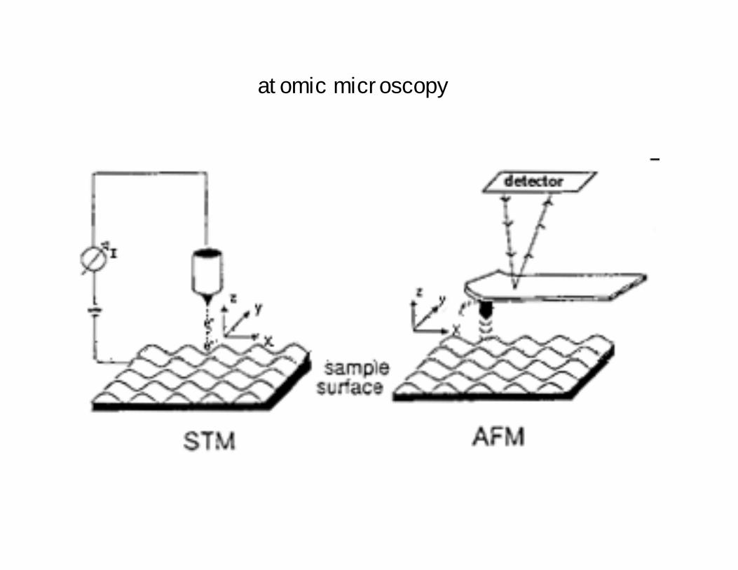
atomic microscopy
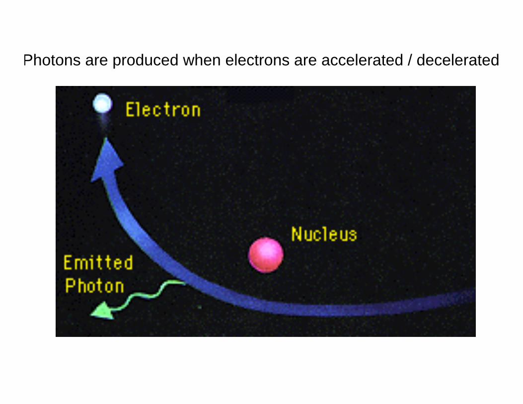
Photons are produced when electrons are accelerated / decelerated
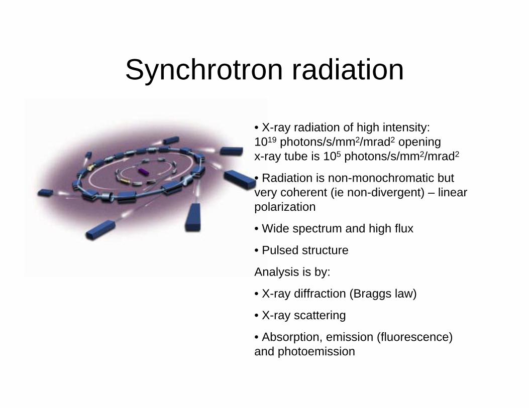
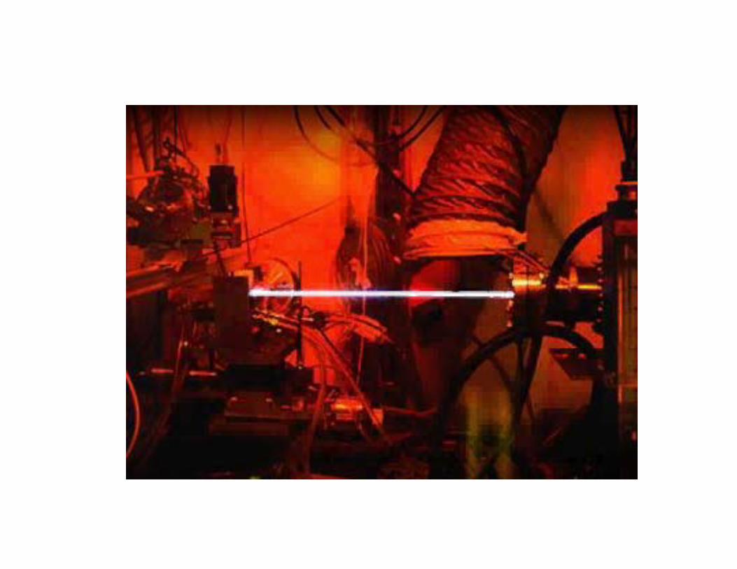
Synchrotron radiation
• X-ray radiation of high intensity:1019 photons/s/mm2/mrad2 openingx-ray tube is 105 photons/s/mm2/mrad2
• Radiation is non-monochromatic butvery coherent (ie non-divergent) – linearpolarization
• Wide spectrum and high flux
• Pulsed structure
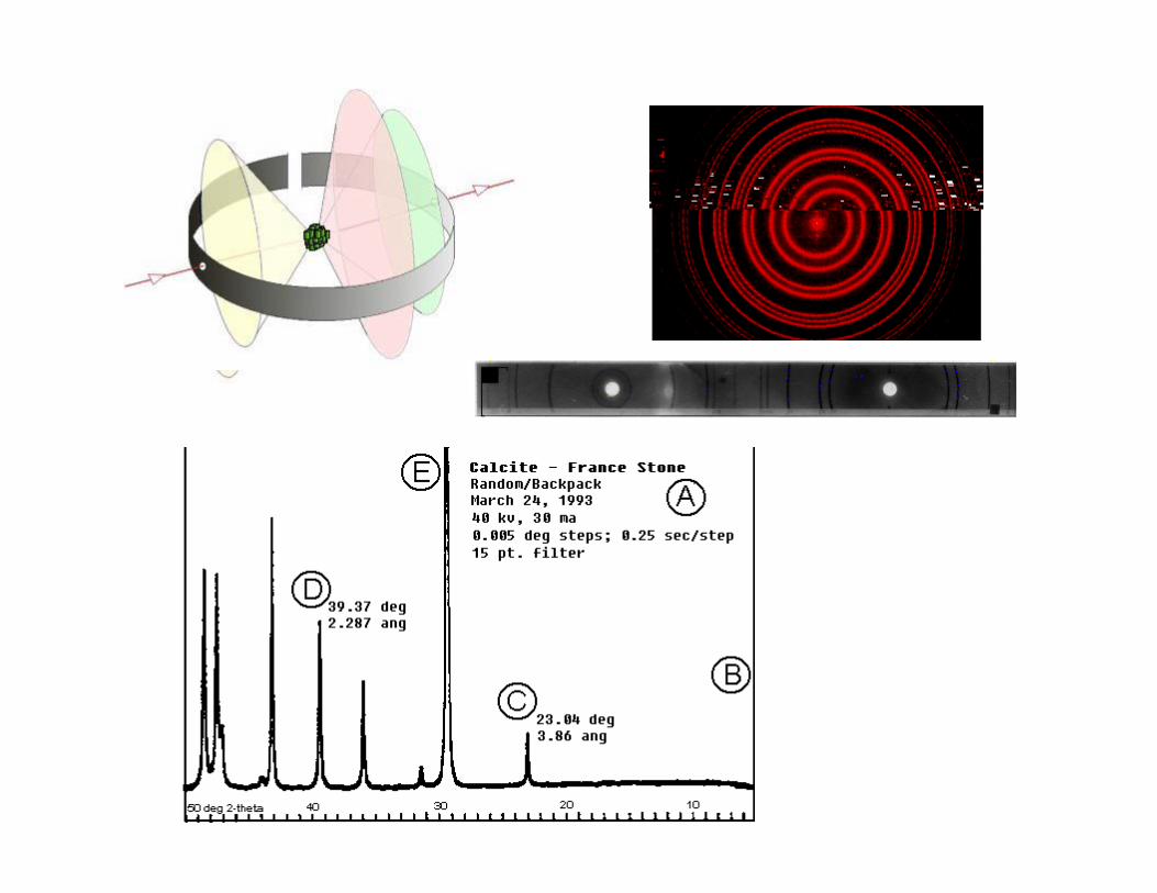
Analysis is by:
• X-ray diffraction (Braggs law)
• X-ray scattering
• Absorption, emission (fluorescence)and photoemission
Yet more power, Igor....
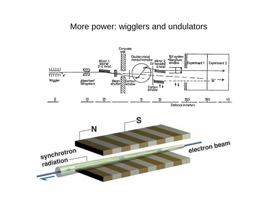
More power: wigglers and undulators
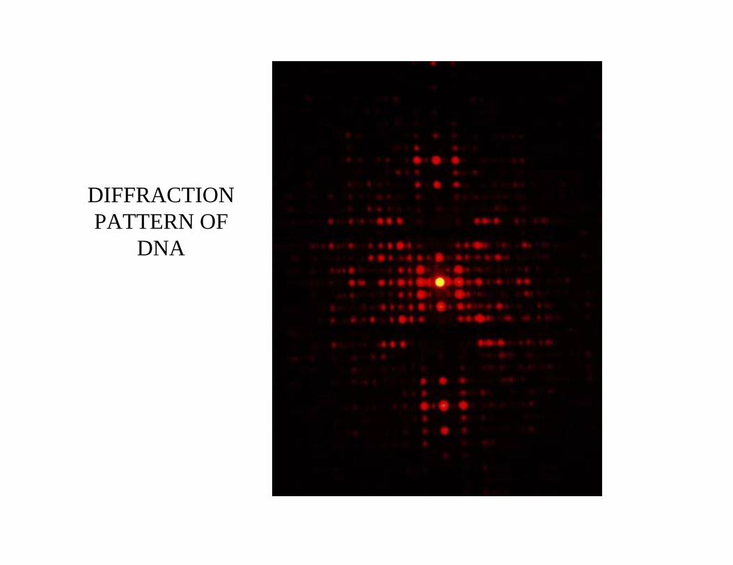
DIFFRACTIONPATTERN OF
DNA
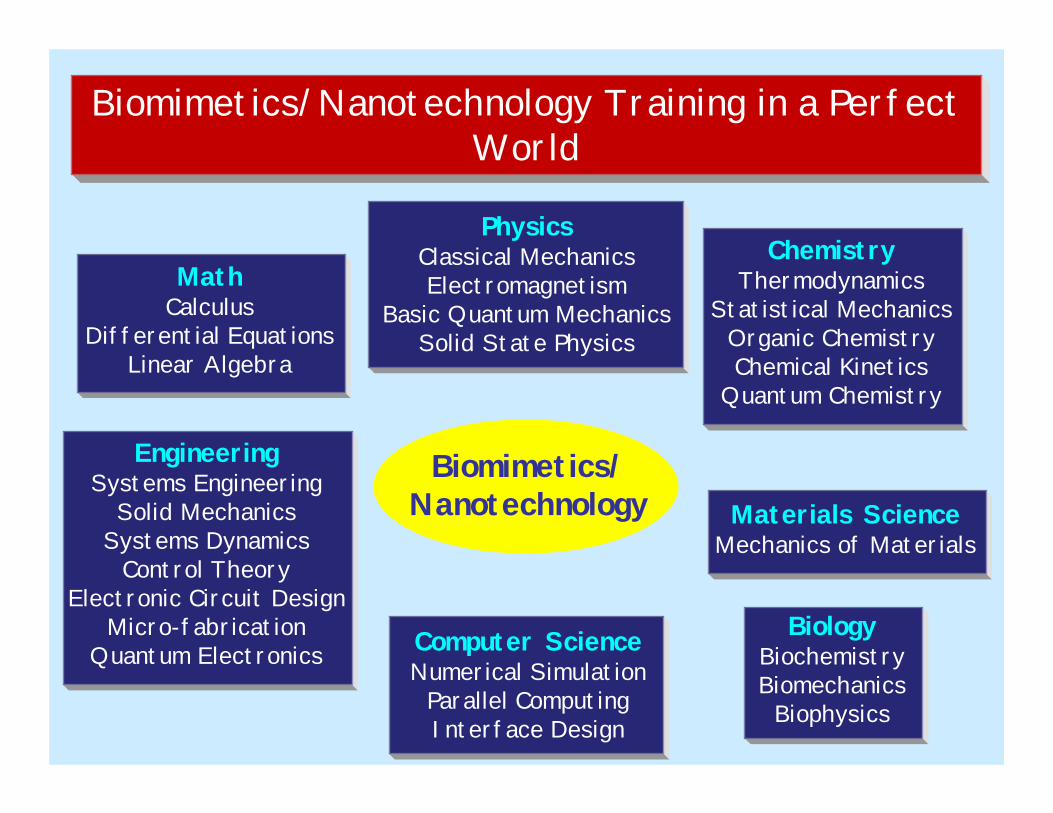
EngineeringSystems Engineering
Solid MechanicsSystems Dynamics
Control TheoryElectronic Circuit Design
Micro-fabricationQuantum Electronics Computer Science
Numerical SimulationParallel ComputingInterface Design
Materials ScienceMechanics of Materials
BiologyBiochemistryBiomechanics
Biophysics
MathCalculus
Differential EquationsLinear Algebra
Biomimetics/Nanotechnology
ChemistryThermodynamics
Statistical MechanicsOrganic ChemistryChemical Kinetics
Quantum Chemistry
PhysicsClassical MechanicsElectromagnetism
Basic Quantum MechanicsSolid State Physics
Biomimetics/Nanotechnology Training in a PerfectWorld
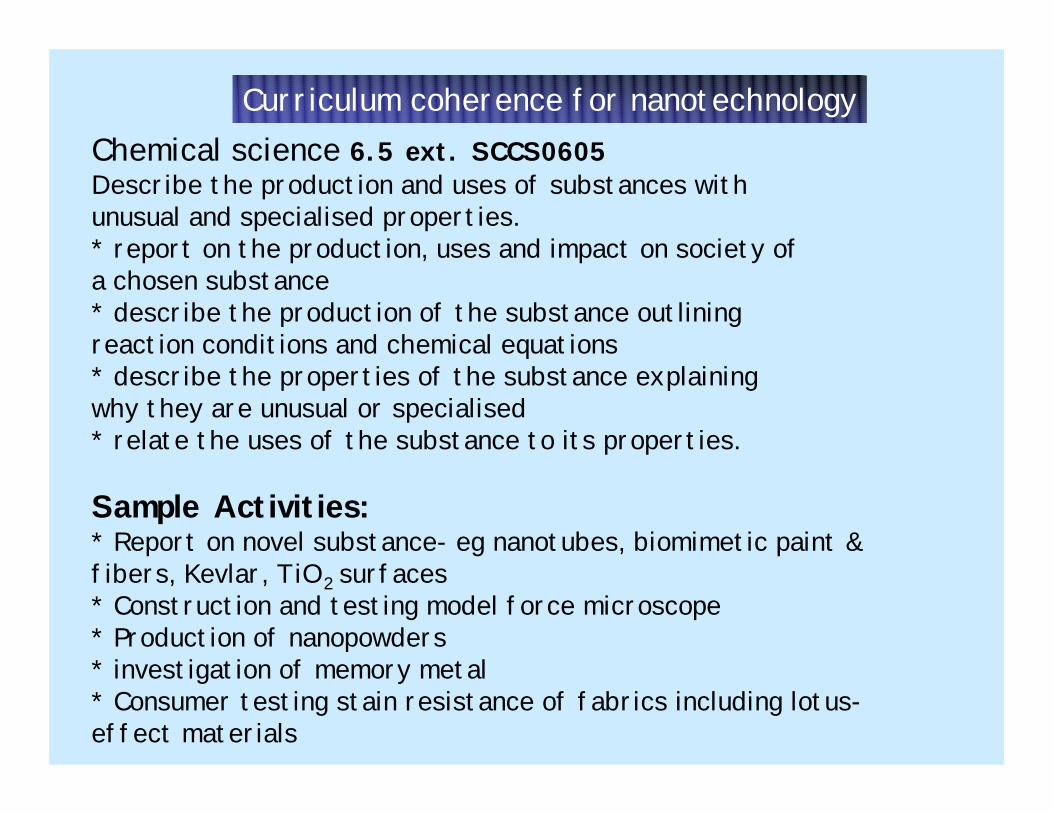
Curriculum coherence for nanotechnologyChemical science 6.5 ext. SCCS0605Describe the production and uses of substances withunusual and specialised properties.* report on the production, uses and impact on society ofa chosen substance* describe the production of the substance outliningreaction conditions and chemical equations* describe the properties of the substance explainingwhy they are unusual or specialised* relate the uses of the substance to its properties.
Sample Activities:* Report on novel substance- eg nanotubes, biomimetic paint &fibers, Kevlar, TiO2 surfaces* Construction and testing model force microscope* Production of nanopowders* investigation of memory metal* Consumer testing stain resistance of fabrics including lotus-effect materials
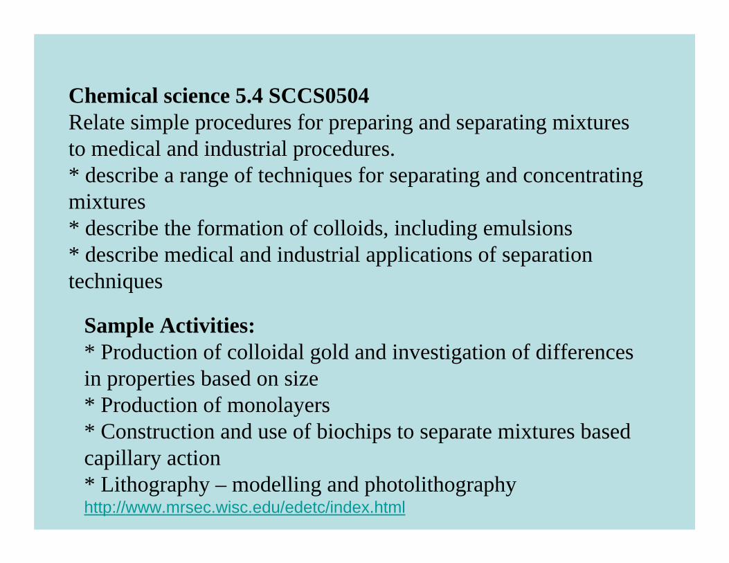
Chemical science 5.4 SCCS0504Relate simple procedures for preparing and separating mixturesto medical and industrial procedures.* describe a range of techniques for separating and concentratingmixtures* describe the formation of colloids, including emulsions* describe medical and industrial applications of separationtechniques
Sample Activities:* Production of colloidal gold and investigation of differencesin properties based on size* Production of monolayers* Construction and use of biochips to separate mixtures basedcapillary action* Lithography – modelling and photolithographyhttp://www.mrsec.wisc.edu/edetc/index.html
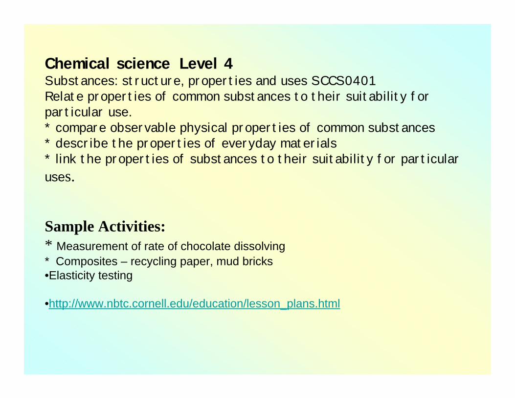
Chemical science Level 4Substances: structure, properties and uses SCCS0401Relate properties of common substances to their suitability forparticular use.* compare observable physical properties of common substances* describe the properties of everyday materials* link the properties of substances to their suitability for particularuses.
Sample Activities:* Measurement of rate of chocolate dissolving* Composites – recycling paper, mud bricks•Elasticity testing
•http://www.nbtc.cornell.edu/education/lesson_plans.html
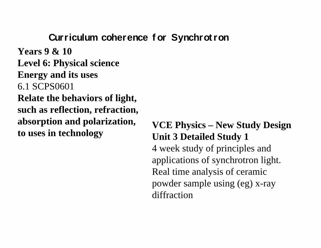
Curriculum coherence for SynchrotronYears 9 & 10Level 6: Physical scienceEnergy and its uses6.1 SCPS0601Relate the behaviors of light,such as reflection, refraction,absorption and polarization,to uses in technology
VCE Physics – New Study DesignUnit 3 Detailed Study 14 week study of principles andapplications of synchrotron light.Real time analysis of ceramicpowder sample using (eg) x-raydiffraction

Opportunities for teachers
• Working with the VCAA and DIIRD,schools have an opportunity toparticipate in the development and trialof curriculum materials and activities inSynchrotron Science or nanotechnology
• Seewww.netspace.net.au/~werry/indexb.htm