nand flash memory - elecfans
TRANSCRIPT

2Gbit x8, x16: NAND Flash Memory
R e v i s i o n : F A x i a M e m o r y T e c h n o l o g y P a g e 1 | 62
NAND Flash Memory
(AX20NV2G8, AX20NV2G6)
Features
• Interface
▪ Open NAND Flash Interface
(ONFI 1.0) compliant
▪ x8, x16
• Technology
▪ Single-level cell (SLC)
▪ 3xnm NAND Process
• Operating Voltage Range
▪ VCC: 2.70V – 3.60V
• Operating Temperature Range
▪ Industrial: -40°C to 85°C
• Packages
▪ 48-pin TSOP (12.0mm x 20mm)
▪ 63-ball FBGA (9mm x 11mm)
• Device Signature
▪ Manufacturer’s ID
▪ Device ID
▪ Device Parameters
▪ Unique ID
• One Time Programmable Area (OTP)
▪ One Block (128K + 4K bytes)
• Quality and Reliability
▪ Recommended Error Correction Code:
4-bit / 528 bytes of data
▪ Data retention: 10 years
▪ Endurance (P/E cycles): 100K (Typ.)
▪ Block zero (block address 00h) is a valid
block when shipped from factory and will
remain valid for at least 1K P/E cycles with
ECC
• Memory Array Organization
▪ x8
• Page size: 2176 bytes
(2048 + 128 bytes)
▪ x16
• Page size: 1088 words
(1024 + 64 words)
▪ Block size: 64 pages
(128K + 8K bytes)
▪ Device size: 2048 blocks (2 Planes)
• Data Protection
▪ WP# signal: write protect entire device
• Device Status
▪ Ready/Busy# (R/B#) signal: hardware
method for detecting internal operation
completion status
• Advanced Command Set
▪ Program page cache mode
▪ Read page cache mode
▪ Page data move (copy back):
▪ Internal data move
▪ Multi-plane Commands
Performance
Device Operation Values Units
Read page 30.0 (Maximum) µs
Program Page 300.0 (Typical) µs
Block Erase 3.5 (Typical) ms
Standby 10.0 (Typical) µA
Read page 15.0 (Typical) mA
2Gbit x8, x16: NAND Flash Memory
R e v i s i o n : F A x i a M e m o r y T e c h n o l o g y P a g e 2 | 62
Table of Contents
Features ...................................................................................................................................................... 1
Performance .............................................................................................................................................. 1
Table of Contents ..................................................................................................................................... 2
General Description ................................................................................................................................. 3
Ordering Options ..................................................................................................................................... 4
Valid Combinations — Standard ...................................................................................................... 4
Signal Description and Assignment ................................................................................................... 5
Package Options ...................................................................................................................................... 6
48-Pin TSOP (Top View) ..................................................................................................................... 6
63-Ball FBGA (Balls Down, Top View) ............................................................................................ 7
Architecture ............................................................................................................................................... 8
Status Register ................................................................................................................................... 11
Bus Interface ........................................................................................................................................... 17
Standby ................................................................................................................................................. 17
Busy ....................................................................................................................................................... 17
Device Protection (Write Protect WP#) ........................................................................................ 17
Command Input .................................................................................................................................. 18
Address Input ...................................................................................................................................... 18
Data Input ............................................................................................................................................. 19
Data Output .......................................................................................................................................... 20
Command Set ...................................................................................................................................... 21
Device Initialization ............................................................................................................................... 53
Device Power-Down .............................................................................................................................. 55
Electrical Specifications ....................................................................................................................... 56
Error Management ................................................................................................................................. 59
ECC Management ................................................................................................................................... 60
Product Use Limitations ....................................................................................................................... 61
Limited Warranty ................................................................................................................................ 61
Revision History ..................................................................................................................................... 62
2Gbit x8, x16: NAND Flash Memory
R e v i s i o n : F A x i a M e m o r y T e c h n o l o g y P a g e 3 | 62
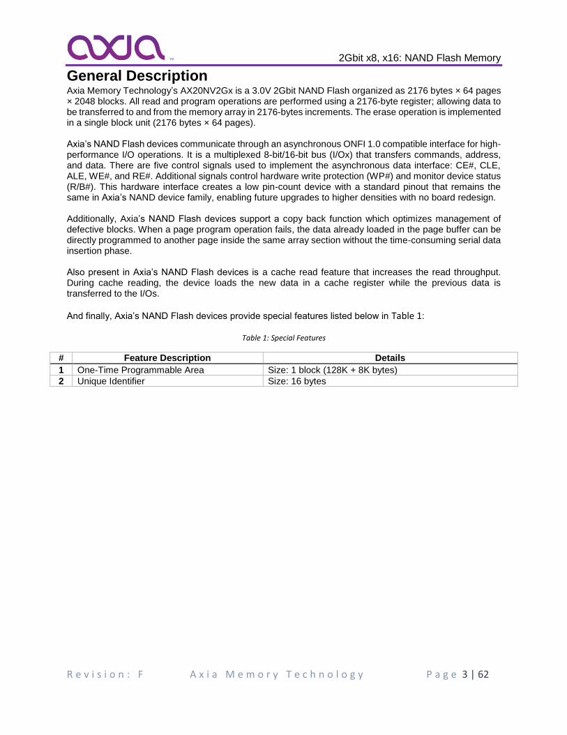
General Description Axia Memory Technology’s AX20NV2Gx is a 3.0V 2Gbit NAND Flash organized as 2176 bytes × 64 pages × 2048 blocks. All read and program operations are performed using a 2176-byte register; allowing data to be transferred to and from the memory array in 2176-bytes increments. The erase operation is implemented in a single block unit (2176 bytes × 64 pages). Axia’s NAND Flash devices communicate through an asynchronous ONFI 1.0 compatible interface for high-performance I/O operations. It is a multiplexed 8-bit/16-bit bus (I/Ox) that transfers commands, address, and data. There are five control signals used to implement the asynchronous data interface: CE#, CLE, ALE, WE#, and RE#. Additional signals control hardware write protection (WP#) and monitor device status (R/B#). This hardware interface creates a low pin-count device with a standard pinout that remains the same in Axia’s NAND device family, enabling future upgrades to higher densities with no board redesign. Additionally, Axia’s NAND Flash devices support a copy back function which optimizes management of defective blocks. When a page program operation fails, the data already loaded in the page buffer can be directly programmed to another page inside the same array section without the time-consuming serial data insertion phase. Also present in Axia’s NAND Flash devices is a cache read feature that increases the read throughput. During cache reading, the device loads the new data in a cache register while the previous data is transferred to the I/Os.
And finally, Axia’s NAND Flash devices provide special features listed below in Table 1:
Table 1: Special Features
# Feature Description Details
1 One-Time Programmable Area Size: 1 block (128K + 8K bytes)
2 Unique Identifier Size: 16 bytes
2Gbit x8, x16: NAND Flash Memory
R e v i s i o n : F A x i a M e m o r y T e c h n o l o g y P a g e 4 | 62
Ordering Options The ordering part numbers are firmed by a valid combination of the following options:
AX 20 N V 2G 8 1 1 TA I 10 1
Packing Type1: Tray
2: Tape & Reel
Special Features
Temperature RangeC: 0°C to +85°C
I: -40°C to +85°C
E: -40°C to +105°C
Package TypeBA: 63-ball WFBGA (9x11x1.0)
TA: 48-pin TSOP
Die Code1
NAND Generation1: 1
st Generation SLC
Bus Width8: x8
6: x16
Density2G: 2Gigabit
Operational VoltageV: 2.70V to 3.60V
E: 1.65V to 1.95V
NAND GradeN: Standard
Product Family20: ONFI NAND
BrandAX: Axia Memory Technology
10: MID Value 1
Valid Combinations — Standard Valid Combinations list includes device configurations currently available. Contact your local sales
office to confirm availability of specific valid combinations and to check on newly released
combinations.
Table 2: Valid Combinations List
Valid Combinations
Base Part Number
Bus Width
Generation Die
Code Package
type Temperature
Range Special
Features Packing
Type Part
Number
AX20NV2G x8 1 1 BA, TA I 10 1, 2 AX20NV2G811BAI101
AX20NV2G811TAI101
AX20NV2G811BAI102
2Gbit x8, x16: NAND Flash Memory
R e v i s i o n : F A x i a M e m o r y T e c h n o l o g y P a g e 5 | 62
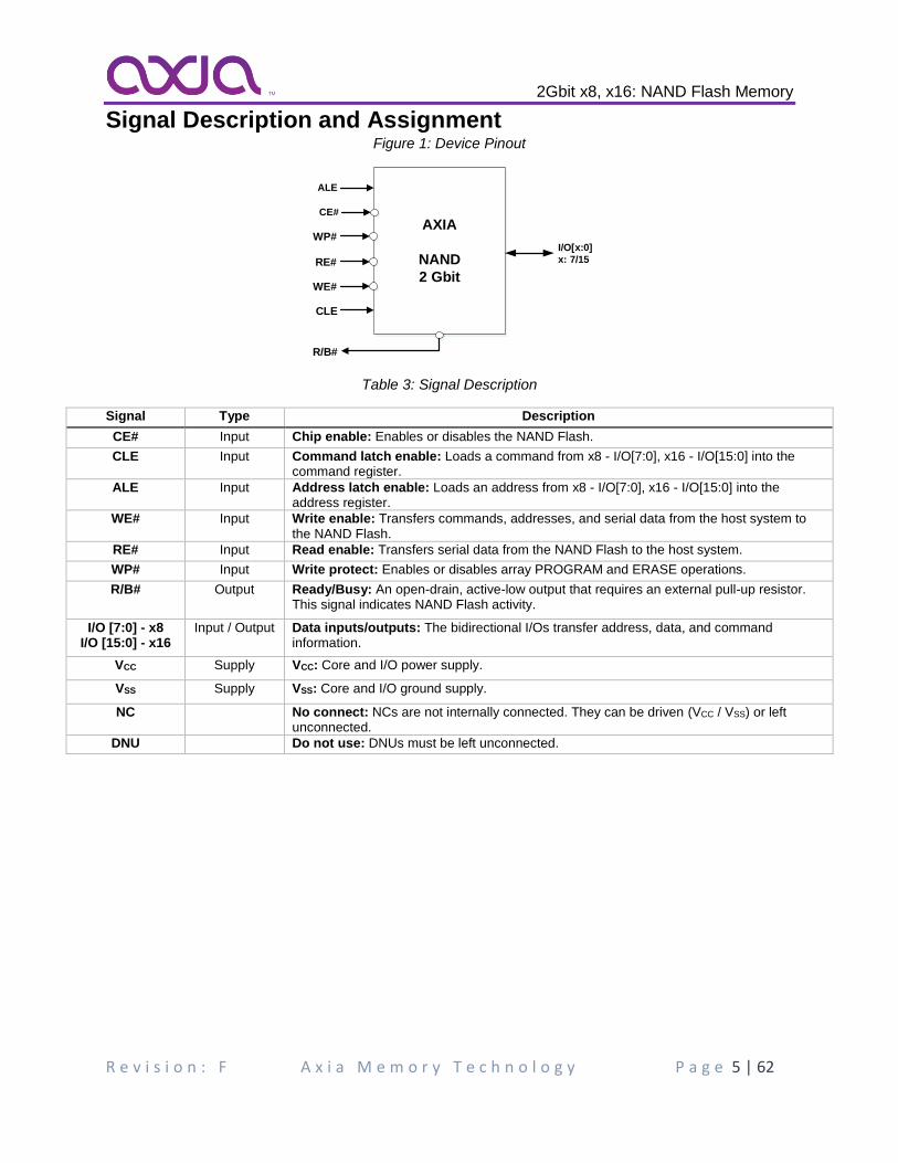
Signal Description and Assignment Figure 1: Device Pinout
AXIA
NAND
2 Gbit
CE#
WP#
RE#
CLE
ALE
R/B#
I/O[x:0]
x: 7/15
WE#
Table 3: Signal Description
Signal Type Description
CE# Input Chip enable: Enables or disables the NAND Flash.
CLE Input Command latch enable: Loads a command from x8 - I/O[7:0], x16 - I/O[15:0] into the command register.
ALE Input Address latch enable: Loads an address from x8 - I/O[7:0], x16 - I/O[15:0] into the address register.
WE# Input Write enable: Transfers commands, addresses, and serial data from the host system to the NAND Flash.
RE# Input Read enable: Transfers serial data from the NAND Flash to the host system.
WP# Input Write protect: Enables or disables array PROGRAM and ERASE operations.
R/B# Output Ready/Busy: An open-drain, active-low output that requires an external pull-up resistor. This signal indicates NAND Flash activity.
I/O [7:0] - x8 I/O [15:0] - x16
Input / Output Data inputs/outputs: The bidirectional I/Os transfer address, data, and command information.
VCC Supply VCC: Core and I/O power supply.
VSS Supply VSS: Core and I/O ground supply.
NC No connect: NCs are not internally connected. They can be driven (VCC / VSS) or left unconnected.
DNU Do not use: DNUs must be left unconnected.
2Gbit x8, x16: NAND Flash Memory
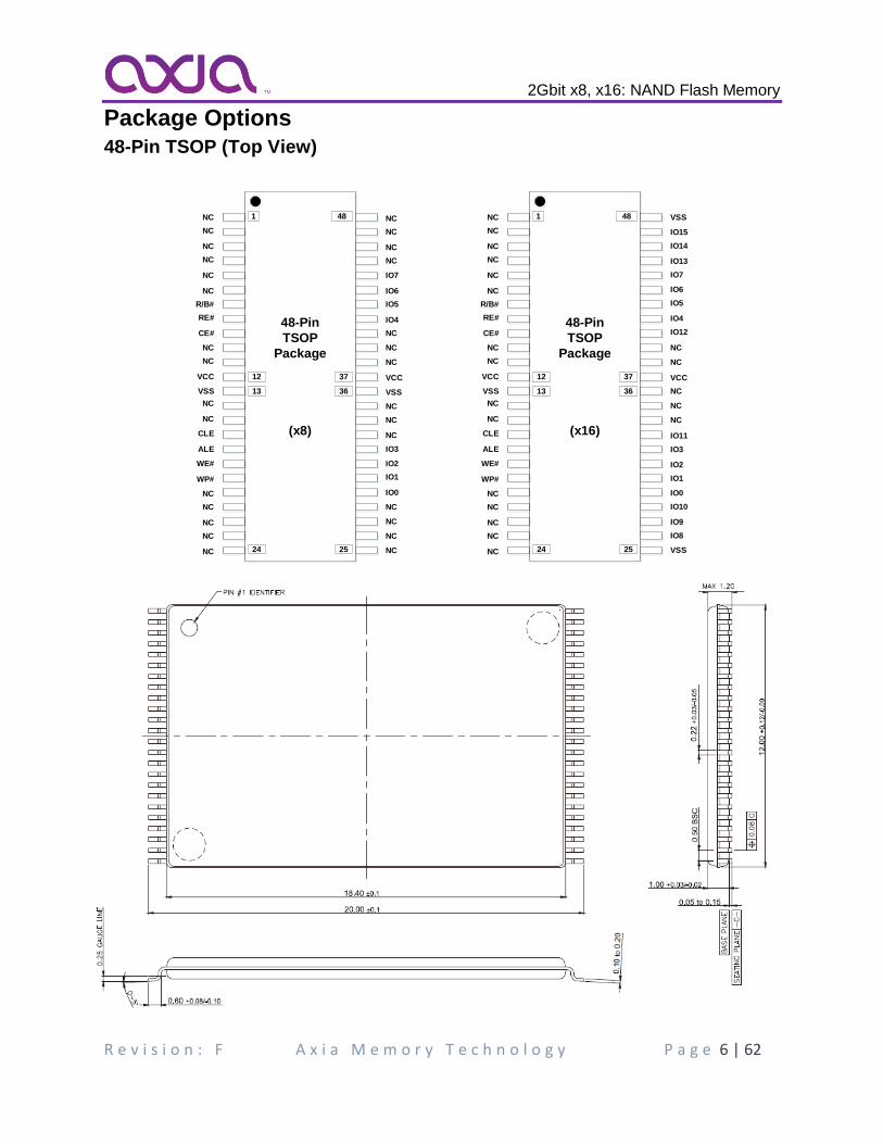
R e v i s i o n : F A x i a M e m o r y T e c h n o l o g y P a g e 6 | 62
Package Options
48-Pin TSOP (Top View)
48-Pin
TSOP
Package
(x8)
text
text
text
text
text
text
text
text
text
text
text
text
text
text
text
text
text
text
text
text
1
12
24
text
text
text
text
text
text
text
text
text
text
text
text
text
text
text
text
text
text
text
text
text
text
text
text
48
36
25
text
text
text
text
R/B#
RE#
CE#
CLE
ALE
WE#
WP#
IO0
IO1
IO2
IO3
IO4
IO5
IO6
NC
VCC
VSS
VCC
VSS
NC
NC
NC
NC
NC
NC
NC
NC
NC
NC
NC
NC
NC
NC
NC
NC
NC
NC
NC
NC
NC
NC
NC
NC
NC
NC
NC
NC
13
37
48-Pin
TSOP
Package
(x16)
text
text
text
text
text
text
text
text
text
text
text
text
text
text
text
text
text
text
text
text
1
12
24
text
text
text
text
text
text
text
text
text
text
text
text
text
text
text
text
text
text
text
text
text
text
text
text
48
36
25
text
text
text
text
R/B#
RE#
CE#
CLE
ALE
WE#
WP#
IO8
IO10
IO1
IO3
VCC
VSS
VCC
VSSNC
NC
NC
NC
NC
NC
NC
NC
NC
NC
NC
NC
NC
NC
NC
13
37
VSS
IO9
IO0
IO2
IO11
IO12
IO5
IO7
IO14
IO4
IO6
IO13
IO15
NC
NC
NC
NC
NC
IO7
2Gbit x8, x16: NAND Flash Memory
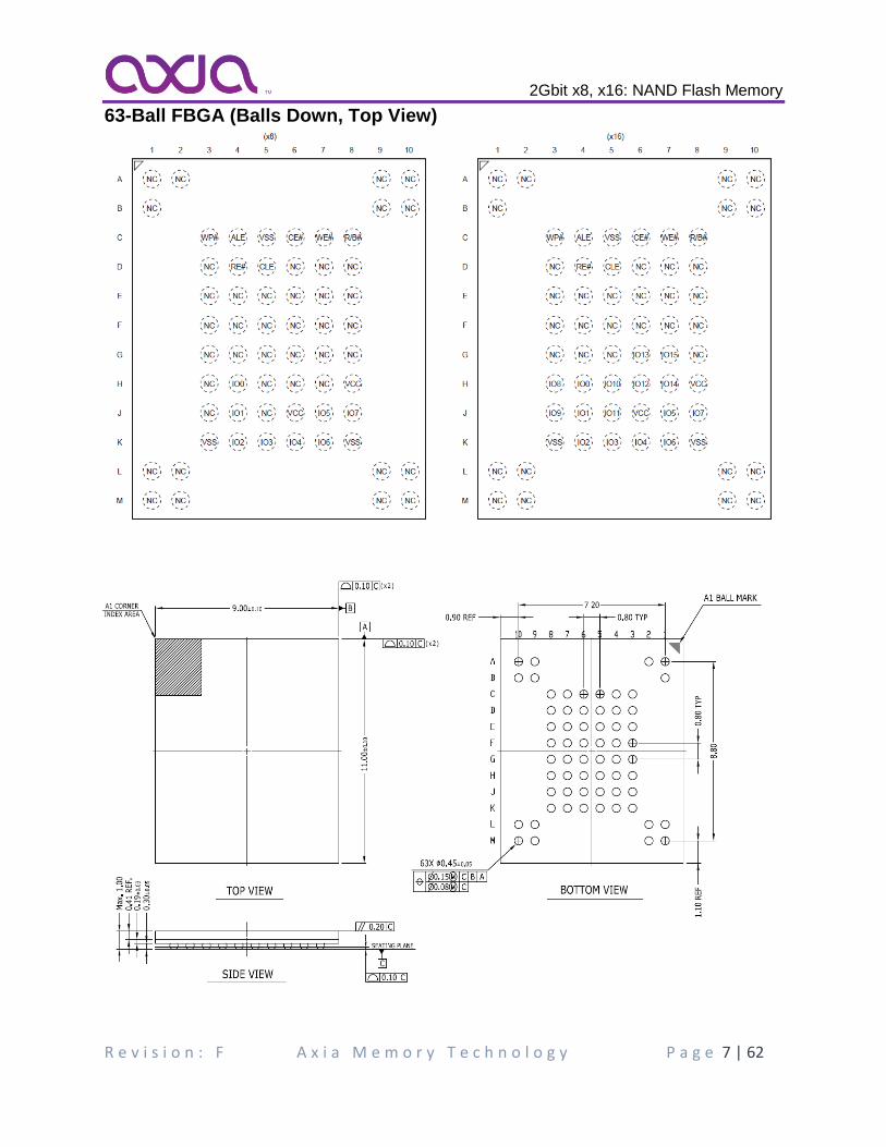
R e v i s i o n : F A x i a M e m o r y T e c h n o l o g y P a g e 7 | 62
63-Ball FBGA (Balls Down, Top View)
2Gbit x8, x16: NAND Flash Memory
R e v i s i o n : F A x i a M e m o r y T e c h n o l o g y P a g e 8 | 62
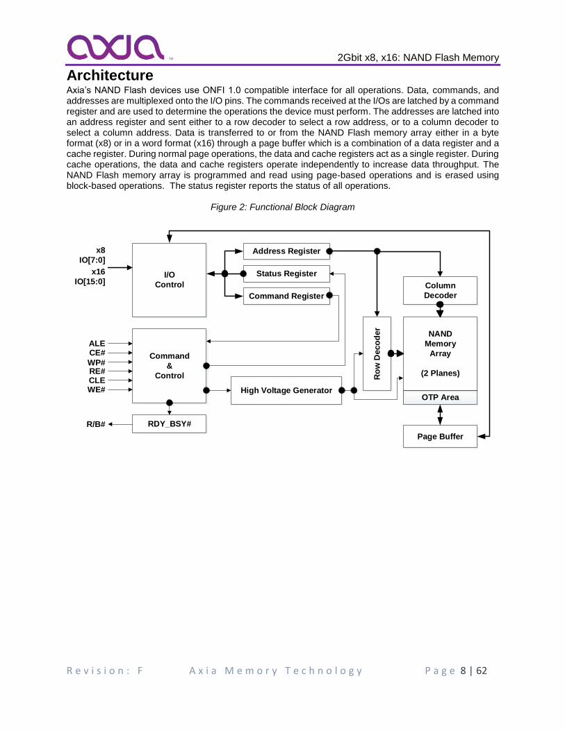
Architecture Axia’s NAND Flash devices use ONFI 1.0 compatible interface for all operations. Data, commands, and addresses are multiplexed onto the I/O pins. The commands received at the I/Os are latched by a command register and are used to determine the operations the device must perform. The addresses are latched into an address register and sent either to a row decoder to select a row address, or to a column decoder to select a column address. Data is transferred to or from the NAND Flash memory array either in a byte format (x8) or in a word format (x16) through a page buffer which is a combination of a data register and a cache register. During normal page operations, the data and cache registers act as a single register. During cache operations, the data and cache registers operate independently to increase data throughput. The NAND Flash memory array is programmed and read using page-based operations and is erased using block-based operations. The status register reports the status of all operations.
Figure 2: Functional Block Diagram
Command
&
Control
CE#
WP#RE#CLE
ALE
NAND
Memory
Array
(2 Planes)R
ow
Deco
der
Column
Decoder
Page Buffer
I/O
Control
Address Register
Status Register
Command Register
High Voltage Generator
RDY_BSY# R/B#
WE#OTP Area
x8
IO[7:0]
x16
IO[15:0]
2Gbit x8, x16: NAND Flash Memory
R e v i s i o n : F A x i a M e m o r y T e c h n o l o g y P a g e 9 | 62
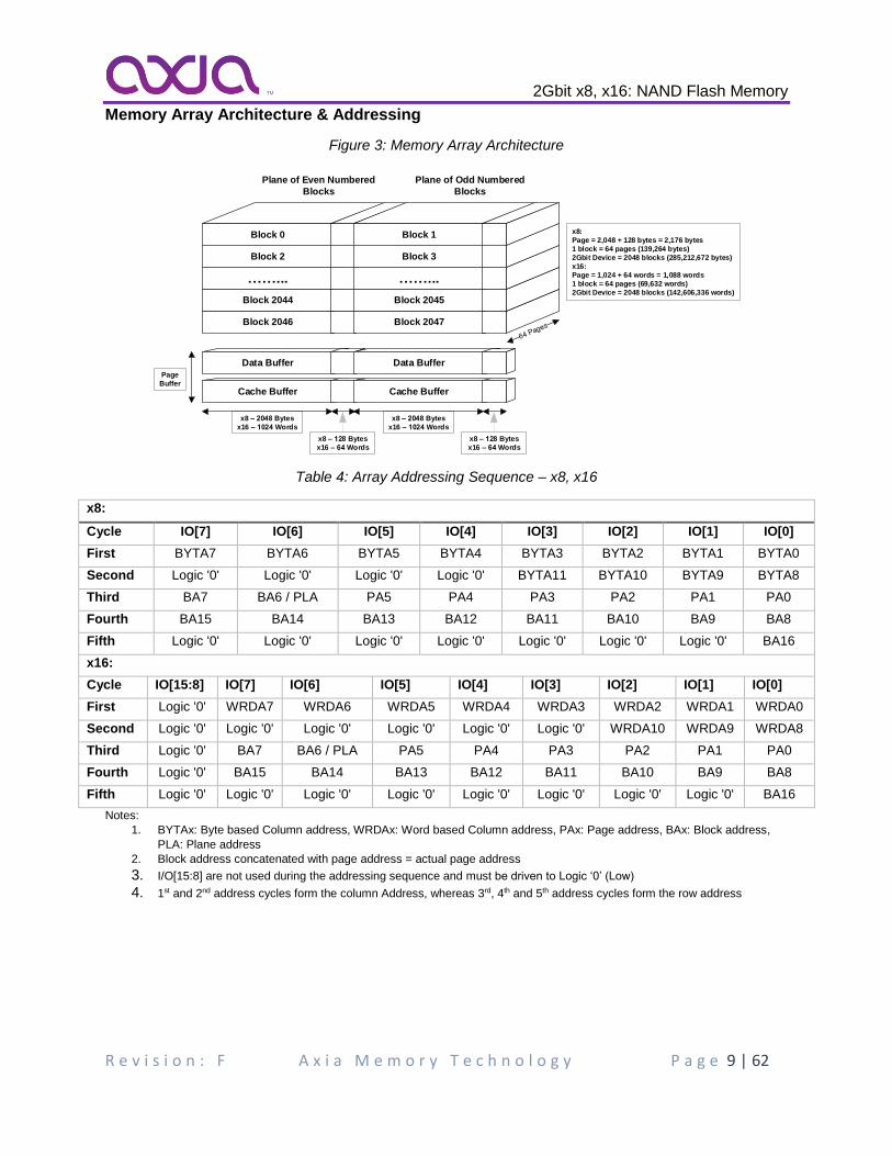
Memory Array Architecture & Addressing
Figure 3: Memory Array Architecture
Block 2046
Block 2044
Block 2
Block 0
Data Buffer
Cache Buffer
x8 – Bytes
x16 – Words
x8 – Bytes
x16 – Words
Page
Buffer
x8:
Page = 2,048 + 128 bytes = 2,176 bytes
1 block = 64 pages (139,264 bytes)
2Gbit Device = 2048 blocks (285,212,672 bytes)
x16:
Page = 1,024 + 64 words = 1,088 words
1 block = 64 pages (69,632 words)
2Gbit Device = 2048 blocks (142,606,336 words)
Block 2047
Block 2045
Block 3
Block 1
Data Buffer
Cache Buffer
x8 – Bytes
x16 – Words
x8 – Bytes
x16 – Words
Plane of Even Numbered
Blocks
Plane of Odd Numbered
Blocks
Table 4: Array Addressing Sequence – x8, x16
x8:
Cycle IO[7] IO[6] IO[5] IO[4] IO[3] IO[2] IO[1] IO[0]
First BYTA7 BYTA6 BYTA5 BYTA4 BYTA3 BYTA2 BYTA1 BYTA0
Second Logic '0' Logic '0' Logic '0' Logic '0' BYTA11 BYTA10 BYTA9 BYTA8
Third BA7 BA6 / PLA PA5 PA4 PA3 PA2 PA1 PA0
Fourth BA15 BA14 BA13 BA12 BA11 BA10 BA9 BA8
Fifth Logic '0' Logic '0' Logic '0' Logic '0' Logic '0' Logic '0' Logic '0' BA16
x16:
Cycle IO[15:8] IO[7] IO[6] IO[5] IO[4] IO[3] IO[2] IO[1] IO[0]
First Logic '0' WRDA7 WRDA6 WRDA5 WRDA4 WRDA3 WRDA2 WRDA1 WRDA0
Second Logic '0' Logic '0' Logic '0' Logic '0' Logic '0' Logic '0' WRDA10 WRDA9 WRDA8
Third Logic '0' BA7 BA6 / PLA PA5 PA4 PA3 PA2 PA1 PA0
Fourth Logic '0' BA15 BA14 BA13 BA12 BA11 BA10 BA9 BA8
Fifth Logic '0' Logic '0' Logic '0' Logic '0' Logic '0' Logic '0' Logic '0' Logic '0' BA16
Notes:
1. BYTAx: Byte based Column address, WRDAx: Word based Column address, PAx: Page address, BAx: Block address,
PLA: Plane address
2. Block address concatenated with page address = actual page address
3. I/O[15:8] are not used during the addressing sequence and must be driven to Logic ‘0’ (Low)
4. 1st and 2nd address cycles form the column Address, whereas 3rd, 4th and 5th address cycles form the row address
2Gbit x8, x16: NAND Flash Memory
R e v i s i o n : F A x i a M e m o r y T e c h n o l o g y P a g e 10 | 62
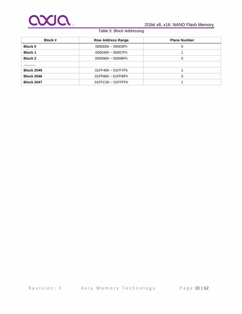
Table 5: Block Addressing
Block # Row Address Range Plane Number
Block 0 000000h ~ 00003Fh 0
Block 1 000040h ~ 00007Fh 1
Block 2 000080h ~ 0000BFh 0
……….
Block 2045 01FF40h ~ 01FF7Fh 1
Block 2046 01FF80h ~ 01FFBFh 0
Block 2047 01FFC0h ~ 01FFFFh 1
2Gbit x8, x16: NAND Flash Memory
R e v i s i o n : F A x i a M e m o r y T e c h n o l o g y P a g e 11 | 62
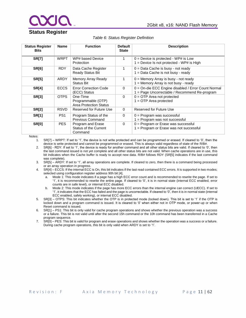
Status Register Table 6: Status Register Definition
Status Register Bits
Name Function Default State
Description
SR[7] WRPT WP# based Device Protection
1 0 = Device is protected - WP# is Low 1 = Device Is not protected - WP# is High
SR[6] RDY Data Cache Register Ready Status Bit
1 0 = Data Cache is busy - not ready 1 = Data Cache is not busy - ready
SR[5] ARDY Memory Array Ready Status Bit
1 0 = Memory Array is busy - not ready 1 = Memory Array is not busy - ready
SR[4] ECCS Error Correction Code (ECC) Status
0 0 = On-die ECC Engine disabled / Error Count Normal 1 = Page Uncorrectable / Recommend Re-program
SR[3] OTPS One-Time Programmable (OTP) Area Protection Status
0 0 = OTP Area not protected 1 = OTP Area protected
SR[2] RSVD Reserved for Future Use 0 Reserved for Future Use
SR[1] PS1 Program Status of the Previous Command
0 0 = Program was successful 1 = Program was not successful
SR[0] PES Program and Erase Status of the Current Command
0 0 = Program or Erase was successful 1 = Program or Erase was not successful
Notes: 1. SR[7] – WRPT: If set to ‘1’, the device is not write protected and can be programmed or erased. If cleared to ‘0’, then the
device is write protected and cannot be programmed or erased. This is always valid regardless of state of the R/B#. 2. SR[6] - RDY: If set to ‘1’, the device is ready for another command and all other status bits are valid. If cleared to ‘0’, then
the last command issued is not yet complete and all other status bits are not valid. When cache operations are in use, this bit indicates when the Cache buffer is ready to accept new data. R/B# follows RDY (SR[5] indicates if the last command was complete).
3. SR[5] – ARDY: If set to ‘1’, all array operations are complete. If cleared to zero, then there is a command being processed or an array operation in progress.
4. SR[4] – ECCS: If the internal ECC is On, this bit indicates if the last read contained ECC errors. It is supported in two modes; selected using configuration register address 90h bit [4].
a. Mode 1: This mode indicates if a page has a high ECC error count and is recommended to rewrite the page. If set to ‘1’, it is recommended to rewrite the entire page. If cleared to ‘0’, it is in normal state (internal ECC enabled, error counts are in safe level), or internal ECC disabled.
b. Mode 2: This mode indicates if the page has more ECC errors than the internal engine can correct (UECC). If set to ‘1’, it indicates that the ECC has failed and the page is uncorrectable. If cleared to ‘0’, then it is in normal state (internal ECC enabled, safely working), or internal ECC disabled.
5. SR[3] – OTPS: This bit indicates whether the OTP is in protected mode (locked down). This bit is set to ‘1’ if the OTP is locked down and a program command is issued. It is cleared to ‘0’ when either not in OTP mode, or power-up or when Reset command is issued.
6. SR[1] – PS1: This bit is only valid for cache program operations and shows whether the previous operation was a success or a failure. This bit is not valid until after the second 15h command or the 10h command has been transferred in a Cache program sequence.
7. SR[0] – PES: This bit is valid for program and erase operations and shows whether the operation was a success or a failure. During cache program operations, this bit is only valid when ARDY is set to ‘1’.
2Gbit x8, x16: NAND Flash Memory
R e v i s i o n : F A x i a M e m o r y T e c h n o l o g y P a g e 12 | 62
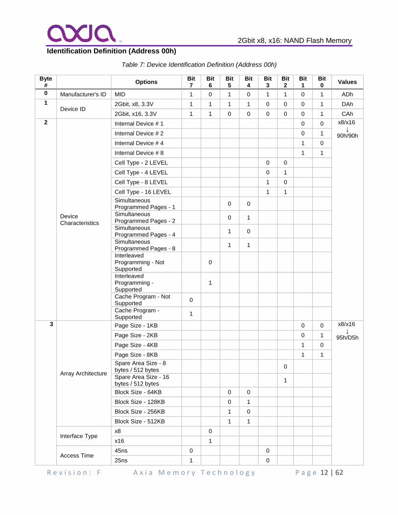
Identification Definition (Address 00h)
Table 7: Device Identification Definition (Address 00h)
Byte #
Options Bit 7
Bit 6
Bit 5
Bit 4
Bit 3
Bit 2
Bit 1
Bit 0
Values
0 Manufacturer's ID MID 1 0 1 0 1 1 0 1 ADh
1 Device ID
2Gbit, x8, 3.3V 1 1 1 1 0 0 0 1 DAh
2Gbit, x16, 3.3V 1 1 0 0 0 0 0 1 CAh
2
Device Characteristics
Internal Device # 1 0 0 x8/x16 ↓
90h/90h
Internal Device # 2 0 1
Internal Device # 4 1 0
Internal Device # 8 1 1
Cell Type - 2 LEVEL 0 0
Cell Type - 4 LEVEL 0 1
Cell Type - 8 LEVEL 1 0
Cell Type - 16 LEVEL 1 1
Simultaneous Programmed Pages - 1
0 0
Simultaneous Programmed Pages - 2
0 1
Simultaneous Programmed Pages - 4
1 0
Simultaneous Programmed Pages - 8
1 1
Interleaved Programming - Not Supported
0
Interleaved Programming - Supported
1
Cache Program - Not Supported
0
Cache Program - Supported
1
3
Array Architecture
Page Size - 1KB 0 0 x8/x16 ↓
95h/D5h
Page Size - 2KB 0 1
Page Size - 4KB 1 0
Page Size - 8KB 1 1
Spare Area Size - 8 bytes / 512 bytes
0
Spare Area Size - 16 bytes / 512 bytes
1
Block Size - 64KB 0 0
Block Size - 128KB 0 1
Block Size - 256KB 1 0
Block Size - 512KB 1 1
Interface Type x8 0
x16 1
Access Time 45ns 0 0
25ns 1 0
2Gbit x8, x16: NAND Flash Memory
R e v i s i o n : F A x i a M e m o r y T e c h n o l o g y P a g e 13 | 62
Byte #
Options Bit 7
Bit 6
Bit 5
Bit 4
Bit 3
Bit 2
Bit 1
Bit 0
Values
Reserved for Future Use
0 1
Reserved for Future Use
1 1
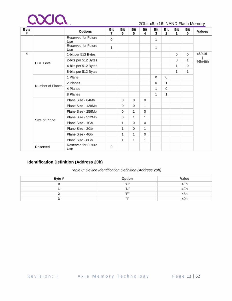
4
ECC Level
1-bit per 512 Bytes 0 0 x8/x16 ↓
46h/46h
2-bits per 512 Bytes 0 1
4-bits per 512 Bytes 1 0
8-bits per 512 Bytes 1 1
Number of Planes
1 Plane 0 0
2 Planes 0 1
4 Planes 1 0
8 Planes 1 1
Size of Plane
Plane Size - 64Mb 0 0 0
Plane Size - 128Mb 0 0 1
Plane Size - 256Mb 0 1 0
Plane Size - 512Mb 0 1 1
Plane Size - 1Gb 1 0 0
Plane Size - 2Gb 1 0 1
Plane Size - 4Gb 1 1 0
Plane Size - 8Gb 1 1 1
Reserved Reserved for Future Use
0
Identification Definition (Address 20h)
Table 8: Device Identification Definition (Address 20h)
Byte # Option Value
0 "O" 4Fh
1 "N" 4Eh
2 "F" 46h
3 "I" 49h
2Gbit x8, x16: NAND Flash Memory
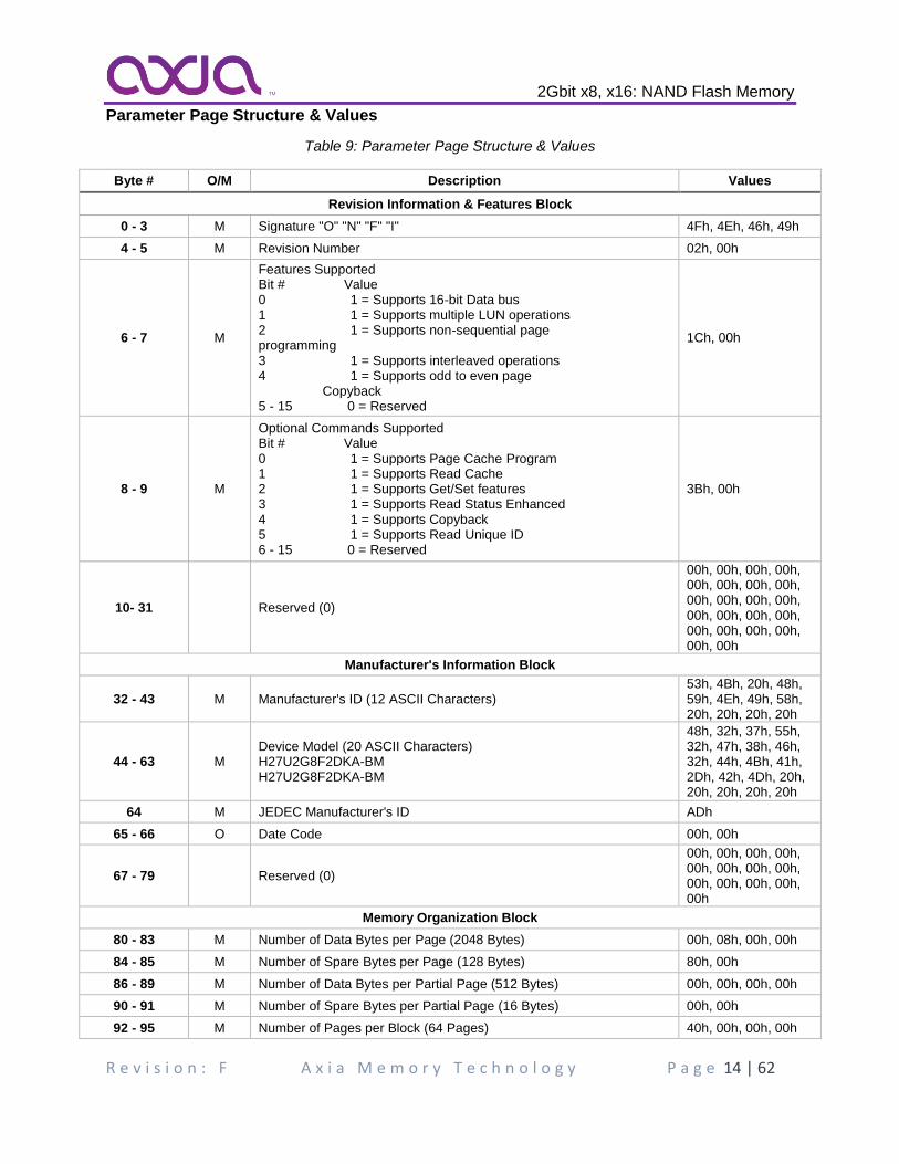
R e v i s i o n : F A x i a M e m o r y T e c h n o l o g y P a g e 14 | 62
Parameter Page Structure & Values
Table 9: Parameter Page Structure & Values
Byte # O/M Description Values
Revision Information & Features Block
0 - 3 M Signature "O" "N" "F" "I" 4Fh, 4Eh, 46h, 49h
4 - 5 M Revision Number 02h, 00h
6 - 7 M
Features Supported Bit # Value 0 1 = Supports 16-bit Data bus 1 1 = Supports multiple LUN operations 2 1 = Supports non-sequential page programming 3 1 = Supports interleaved operations 4 1 = Supports odd to even page Copyback 5 - 15 0 = Reserved
1Ch, 00h
8 - 9 M
Optional Commands Supported Bit # Value 0 1 = Supports Page Cache Program 1 1 = Supports Read Cache 2 1 = Supports Get/Set features 3 1 = Supports Read Status Enhanced 4 1 = Supports Copyback 5 1 = Supports Read Unique ID 6 - 15 0 = Reserved
3Bh, 00h
10- 31 Reserved (0)
00h, 00h, 00h, 00h, 00h, 00h, 00h, 00h, 00h, 00h, 00h, 00h, 00h, 00h, 00h, 00h, 00h, 00h, 00h, 00h, 00h, 00h
Manufacturer's Information Block
32 - 43 M Manufacturer's ID (12 ASCII Characters) 53h, 4Bh, 20h, 48h, 59h, 4Eh, 49h, 58h, 20h, 20h, 20h, 20h
44 - 63 M Device Model (20 ASCII Characters) H27U2G8F2DKA-BM H27U2G8F2DKA-BM
48h, 32h, 37h, 55h, 32h, 47h, 38h, 46h, 32h, 44h, 4Bh, 41h, 2Dh, 42h, 4Dh, 20h, 20h, 20h, 20h, 20h
64 M JEDEC Manufacturer's ID ADh
65 - 66 O Date Code 00h, 00h
67 - 79 Reserved (0)
00h, 00h, 00h, 00h, 00h, 00h, 00h, 00h, 00h, 00h, 00h, 00h, 00h
Memory Organization Block
80 - 83 M Number of Data Bytes per Page (2048 Bytes) 00h, 08h, 00h, 00h
84 - 85 M Number of Spare Bytes per Page (128 Bytes) 80h, 00h
86 - 89 M Number of Data Bytes per Partial Page (512 Bytes) 00h, 00h, 00h, 00h
90 - 91 M Number of Spare Bytes per Partial Page (16 Bytes) 00h, 00h
92 - 95 M Number of Pages per Block (64 Pages) 40h, 00h, 00h, 00h
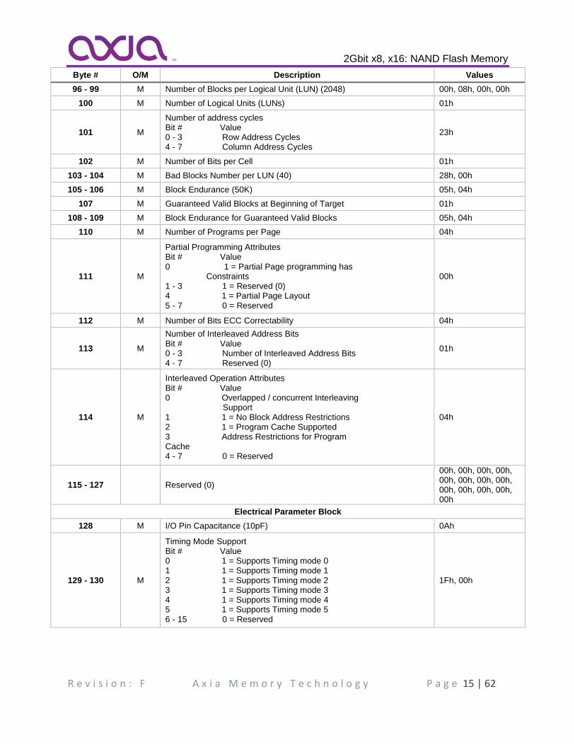
2Gbit x8, x16: NAND Flash Memory
R e v i s i o n : F A x i a M e m o r y T e c h n o l o g y P a g e 15 | 62
Byte # O/M Description Values
96 - 99 M Number of Blocks per Logical Unit (LUN) (2048) 00h, 08h, 00h, 00h
100 M Number of Logical Units (LUNs) 01h
101 M
Number of address cycles Bit # Value 0 - 3 Row Address Cycles 4 - 7 Column Address Cycles
23h
102 M Number of Bits per Cell 01h
103 - 104 M Bad Blocks Number per LUN (40) 28h, 00h
105 - 106 M Block Endurance (50K) 05h, 04h
107 M Guaranteed Valid Blocks at Beginning of Target 01h
108 - 109 M Block Endurance for Guaranteed Valid Blocks 05h, 04h
110 M Number of Programs per Page 04h
111 M
Partial Programming Attributes Bit # Value 0 1 = Partial Page programming has Constraints 1 - 3 1 = Reserved (0) 4 1 = Partial Page Layout 5 - 7 0 = Reserved
00h
112 M Number of Bits ECC Correctability 04h
113 M
Number of Interleaved Address Bits Bit # Value 0 - 3 Number of Interleaved Address Bits 4 - 7 Reserved (0)
01h
114 M
Interleaved Operation Attributes Bit # Value 0 Overlapped / concurrent Interleaving Support 1 1 = No Block Address Restrictions 2 1 = Program Cache Supported 3 Address Restrictions for Program Cache 4 - 7 0 = Reserved
04h
115 - 127 Reserved (0)
00h, 00h, 00h, 00h, 00h, 00h, 00h, 00h, 00h, 00h, 00h, 00h, 00h
Electrical Parameter Block
128 M I/O Pin Capacitance (10pF) 0Ah
129 - 130 M
Timing Mode Support Bit # Value 0 1 = Supports Timing mode 0 1 1 = Supports Timing mode 1 2 1 = Supports Timing mode 2 3 1 = Supports Timing mode 3 4 1 = Supports Timing mode 4 5 1 = Supports Timing mode 5 6 - 15 0 = Reserved
1Fh, 00h
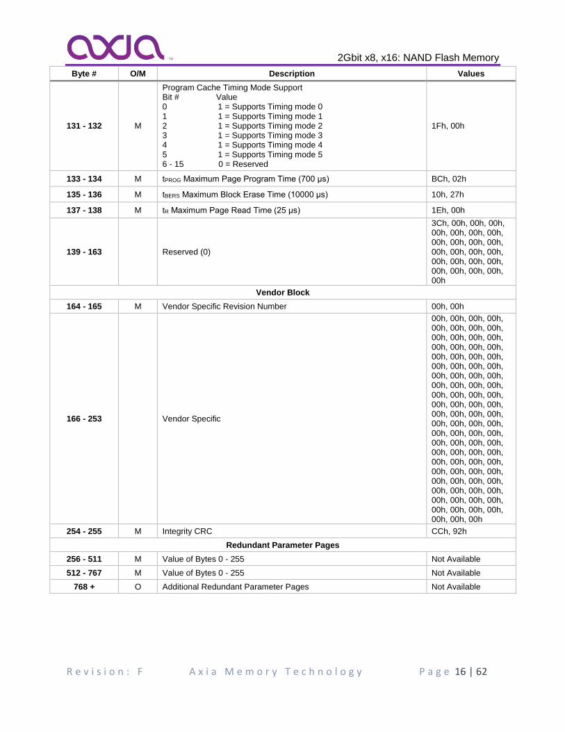
2Gbit x8, x16: NAND Flash Memory
R e v i s i o n : F A x i a M e m o r y T e c h n o l o g y P a g e 16 | 62
Byte # O/M Description Values
131 - 132 M
Program Cache Timing Mode Support Bit # Value 0 1 = Supports Timing mode 0 1 1 = Supports Timing mode 1 2 1 = Supports Timing mode 2 3 1 = Supports Timing mode 3 4 1 = Supports Timing mode 4 5 1 = Supports Timing mode 5 6 - 15 0 = Reserved
1Fh, 00h
133 - 134 M tPROG Maximum Page Program Time (700 μs) BCh, 02h
135 - 136 M tBERS Maximum Block Erase Time (10000 μs) 10h, 27h
137 - 138 M tR Maximum Page Read Time (25 μs) 1Eh, 00h
139 - 163 Reserved (0)
3Ch, 00h, 00h, 00h, 00h, 00h, 00h, 00h, 00h, 00h, 00h, 00h, 00h, 00h, 00h, 00h, 00h, 00h, 00h, 00h, 00h, 00h, 00h, 00h, 00h
Vendor Block
164 - 165 M Vendor Specific Revision Number 00h, 00h
166 - 253 Vendor Specific
00h, 00h, 00h, 00h, 00h, 00h, 00h, 00h, 00h, 00h, 00h, 00h, 00h, 00h, 00h, 00h, 00h, 00h, 00h, 00h, 00h, 00h, 00h, 00h, 00h, 00h, 00h, 00h, 00h, 00h, 00h, 00h, 00h, 00h, 00h, 00h, 00h, 00h, 00h, 00h, 00h, 00h, 00h, 00h, 00h, 00h, 00h, 00h, 00h, 00h, 00h, 00h, 00h, 00h, 00h, 00h, 00h, 00h, 00h, 00h, 00h, 00h, 00h, 00h, 00h, 00h, 00h, 00h, 00h, 00h, 00h, 00h, 00h, 00h, 00h, 00h, 00h, 00h, 00h, 00h, 00h, 00h, 00h, 00h, 00h, 00h, 00h
254 - 255 M Integrity CRC CCh, 92h
Redundant Parameter Pages
256 - 511 M Value of Bytes 0 - 255 Not Available
512 - 767 M Value of Bytes 0 - 255 Not Available
768 + O Additional Redundant Parameter Pages Not Available
2Gbit x8, x16: NAND Flash Memory
R e v i s i o n : F A x i a M e m o r y T e c h n o l o g y P a g e 17 | 62
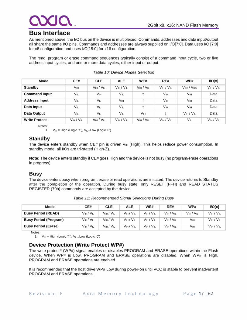
Bus Interface As mentioned above, the I/O bus on the device is multiplexed. Commands, addresses and data input/output all share the same I/O pins. Commands and addresses are always supplied on I/O[7:0]. Data uses I/O [7:0] for x8 configuration and uses I/O[15:0] for x16 configuration. The read, program or erase command sequences typically consist of a command input cycle, two or five address input cycles, and one or more data cycles, either input or output.
Table 10: Device Modes Selection
Mode CE# CLE ALE WE# RE# WP# I/O[x]
Standby VIH VIH / VIL VIH / VIL VIH / VIL VIH / VIL VCC / VSS VIH / VIL
Command Input VIL VIH VIL ↑ VIH VIH Data
Address Input VIL VIL VIH ↑ VIH VIH Data
Data Input VIL VIL VIL ↑ VIH VIH Data
Data Output VIL VIL VIL VIH ↓ VIH / VIL Data
Write Protect VIH / VIL VIH / VIL VIH / VIL VIH / VIL VIH / VIL VIL VIH / VIL
Notes:
1. VIH = High (Logic ‘1’), VIL = Low (Logic ‘0’)
Standby The device enters standby when CE# pin is driven VIH (High). This helps reduce power consumption. In standby mode, all I/Os are tri-stated (High-Z). Note: The device enters standby if CE# goes High and the device is not busy (no program/erase operations in progress).
Busy The device enters busy when program, erase or read operations are initiated. The device returns to Standby after the completion of the operation. During busy state, only RESET (FFH) and READ STATUS REGISTER (70h) commands are accepted by the device.
Table 11: Recommended Signal Selections During Busy
Mode CE# CLE ALE WE# RE# WP# I/O[x]
Busy Period (READ) VIH / VIL VIH / VIL VIH / VIL VIH / VIL VIH / VIL VIH / VIL VIH / VIL
Busy Period (Program) VIH / VIL VIH / VIL VIH / VIL VIH / VIL VIH / VIL VIH VIH / VIL
Busy Period (Erase) VIH / VIL VIH / VIL VIH / VIL VIH / VIL VIH / VIL VIH VIH / VIL
Notes:
1. VIH = High (Logic ‘1’), VIL = Low (Logic ‘0’)
Device Protection (Write Protect WP#) The write protect# (WP#) signal enables or disables PROGRAM and ERASE operations within the Flash device. When WP# is Low, PROGRAM and ERASE operations are disabled. When WP# is High, PROGRAM and ERASE operations are enabled. It is recommended that the host drive WP# Low during power-on until VCC is stable to prevent inadvertent PROGRAM and ERASE operations.
2Gbit x8, x16: NAND Flash Memory
R e v i s i o n : F A x i a M e m o r y T e c h n o l o g y P a g e 18 | 62
WP# must be transitioned only when the device is in Standby and prior to beginning a command sequence. After a command sequence is complete and the device is ready, WP# can be transitioned. After WP# is transitioned, the host must wait tWW before issuing a new command. The WP# signal is always an active input, even when CE# is High. This signal should not be multiplexed with other signals.
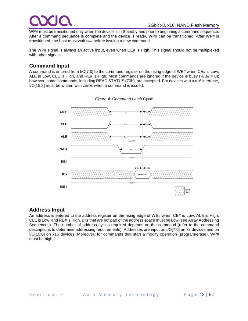
Command Input A command is entered from I/O[7:0] to the command register on the rising edge of WE# when CE# is Low, ALE is Low, CLE is High, and RE# is High. Most commands are ignored if the device is busy (R/B# = 0); however, some commands, including READ STATUS (70h), are accepted. For devices with a x16 interface, I/O[15:8] must be written with zeros when a command is issued.
Figure 4: Command Latch Cycle
CE#
CLE
Logic
ALE
WE#
Logic
RE#
IOx
Logic
R/B#
tDHtDS
Command
Don tCare
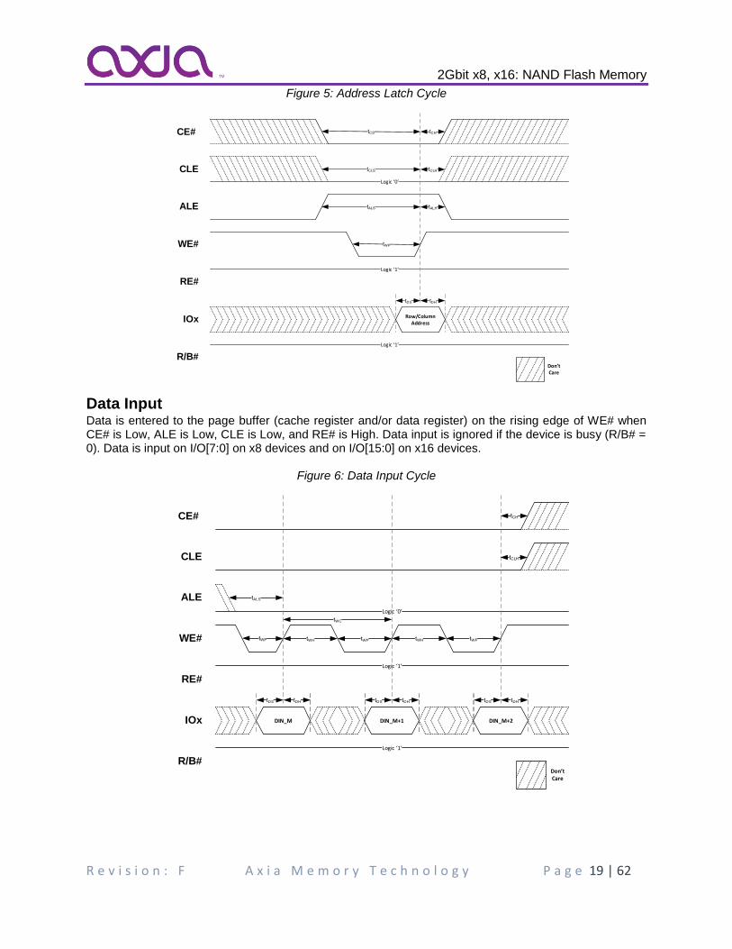
Address Input An address is entered to the address register on the rising edge of WE# when CE# is Low, ALE is High, CLE is Low, and RE# is High. Bits that are not part of the address space must be Low (see Array Addressing Sequences). The number of address cycles required depends on the command (refer to the command descriptions to determine addressing requirements). Addresses are input on I/O[7:0] on x8 devices and on I/O[15:0] on x16 devices. Moreover, for commands that start a modify operation (program/erase), WP# must be high.
2Gbit x8, x16: NAND Flash Memory
R e v i s i o n : F A x i a M e m o r y T e c h n o l o g y P a g e 19 | 62
Figure 5: Address Latch Cycle
CE#
CLELogic
ALE
WE#
Logic
RE#
IOx
Logic
R/B#
tDHtDS
Row/ColumnAddress
Don tCare
Data Input Data is entered to the page buffer (cache register and/or data register) on the rising edge of WE# when CE# is Low, ALE is Low, CLE is Low, and RE# is High. Data input is ignored if the device is busy (R/B# = 0). Data is input on I/O[7:0] on x8 devices and on I/O[15:0] on x16 devices.
Figure 6: Data Input Cycle
CE#
CLE
Logic
ALE
WE#
Logic
RE#
IOx
Logic
R/B#
tALS
Don tCare
tDHtDS
DIN_M+1
tDHtDS
DIN_M
tDHtDS
DIN_M+2
tWP
tWC
tWHtWPtWH
2Gbit x8, x16: NAND Flash Memory
R e v i s i o n : F A x i a M e m o r y T e c h n o l o g y P a g e 20 | 62
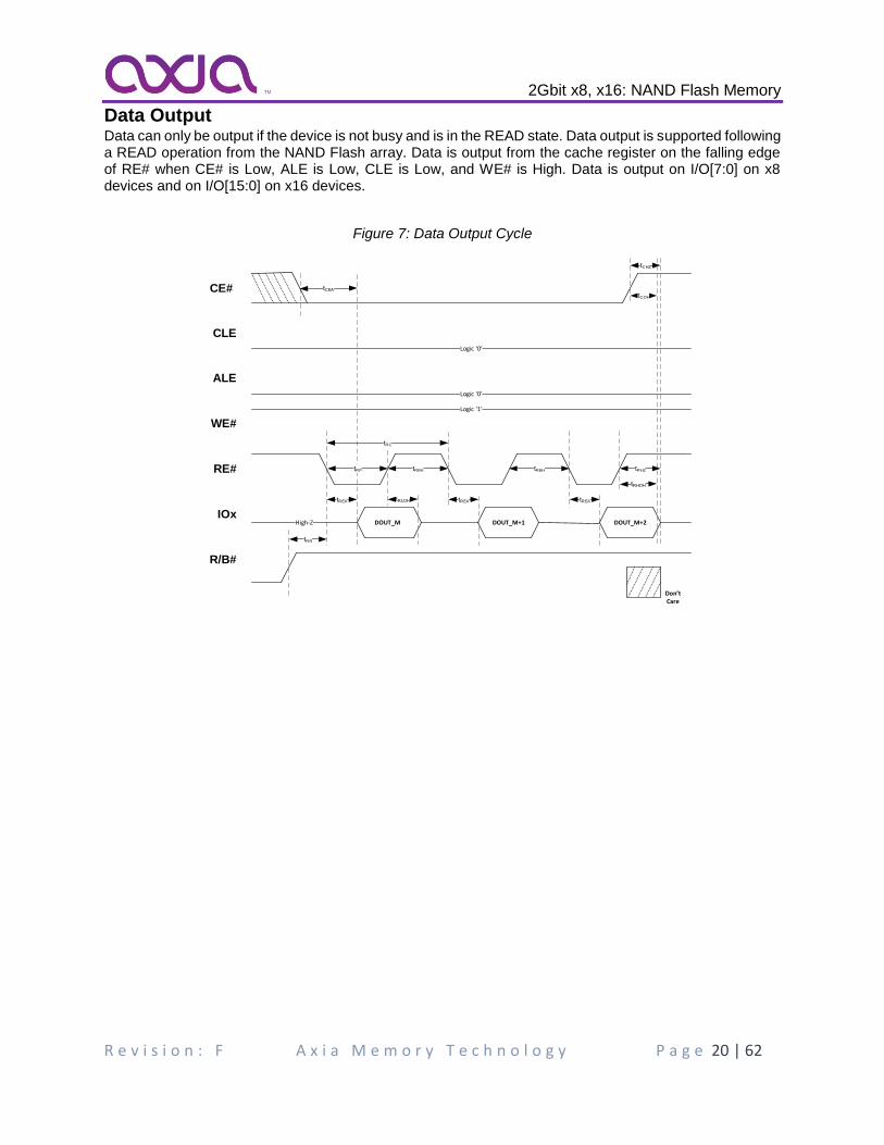
Data Output Data can only be output if the device is not busy and is in the READ state. Data output is supported following a READ operation from the NAND Flash array. Data is output from the cache register on the falling edge of RE# when CE# is Low, ALE is Low, CLE is Low, and WE# is High. Data is output on I/O[7:0] on x8 devices and on I/O[15:0] on x16 devices.
Figure 7: Data Output Cycle
CE#
CLELogic
Logic
ALE
WE#
Logic
RE#
IOx
R/B#
tCHZ
Don tCare
DOUT_M+1
tREA
DOUT_M DOUT_M+2
tRC
tREHtREH
tREA tREA
High-Z
tRHZ
tCOH
tRR
tRP
2Gbit x8, x16: NAND Flash Memory
R e v i s i o n : F A x i a M e m o r y T e c h n o l o g y P a g e 21 | 62
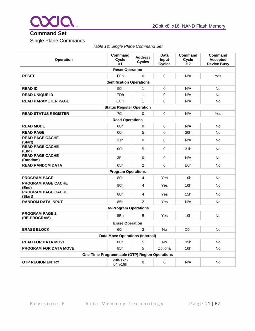
Command Set
Single Plane Commands Table 12: Single Plane Command Set
Operation Command
Cycle #1
Address Cycles
Data Input
Cycles
Command Cycle
# 2
Command Accepted
Device Busy
Reset Operation
RESET FFh 0 0 N/A Yes
Identification Operations
READ ID 90h 1 0 N/A No
READ UNIQUE ID EDh 1 0 N/A No
READ PARAMETER PAGE ECH 1 0 N/A No
Status Register Operation
READ STATUS REGISTER 70h 0 0 N/A Yes
Read Operations
READ MODE 00h 0 0 N/A No
READ PAGE 00h 5 0 30h No
READ PAGE CACHE (Start)
31h 0 0 N/A No
READ PAGE CACHE (End)
00h 5 0 31h No
READ PAGE CACHE (Random)
3Fh 0 0 N/A No
READ RANDOM DATA 05h 2 0 E0h No
Program Operations
PROGRAM PAGE 80h 4 Yes 10h No
PROGRAM PAGE CACHE (End)
80h 4 Yes 10h No
PROGRAM PAGE CACHE (Start)
80h 4 Yes 15h No
RANDOM DATA INPUT 85h 2 Yes N/A No
Re-Program Operations
PROGRAM PAGE 2 (RE-PROGRAM)
8Bh 5 Yes 10h No
Erase Operation
ERASE BLOCK 60h 3 No D0h No
Data Move Operations (Internal)
READ FOR DATA MOVE 00h 5 No 35h No
PROGRAM FOR DATA MOVE 85h 5 Optional 10h No
One-Time Programmable (OTP) Region Operations
OTP REGION ENTRY 29h-17h- 04h-19h
0 0 N/A No
2Gbit x8, x16: NAND Flash Memory
R e v i s i o n : F A x i a M e m o r y T e c h n o l o g y P a g e 22 | 62
Multi-Plane (MP) / Multi-Device (MD) Commands Table 13: Multi-Plane / Multi-Device Command Set
Operation CMD Cycle
#1
ADDR Cycles
CMD Cycle
#2
ADDR Cycles
CMD Cycle
#2
ADDR Cycles
CADB
Program Operations
PROGRAM PAGE MP 80h 80h
5 5
11h - 81h 11h - 80h
5 5
10h 10h
- No
PROGRAM PAGE CACHE MP (END) 80h 80h
5 5
11h - 81h 11h - 80h
5 5
10h 10h
- No
PROGRAM PAGE CACHE MP 80h 80h
5 5
11h - 81h 11h - 80h
5 5
15h 15h
- No
Erase Operations
ERASE BLOCK MP 60h 60h
3 3
60h D1h - 60h
3 3
D0h D0h
- No
Data Move Operations (Internal)
PROGRAM FOR DATA MOVE MP 85h 85h
5 5
11h - 81h 11h - 85h
5 5
10h 10h
- No
Status Register Operation
READ STATUS REGISTER MP/MD 78h 3 - - - - Yes
RESET Operation (FFh) The RESET command (FFh) places the NAND Flash device into the standby mode and aborts any command sequence in progress. READ, PROGRAM, and ERASE commands can be aborted while the device is in the busy state using the RESET command. The contents of the memory location being programmed, or the block being erased are no longer valid - the data may be partially erased or programmed and is invalid. The command register is cleared and is ready for the next command. The data register and cache register contents are marked invalid. The status register contains the value E0h when WP# is High; otherwise it contains the value 60h. R/B# goes Low for tRST during which the device completes the reset operation.
2Gbit x8, x16: NAND Flash Memory
R e v i s i o n : F A x i a M e m o r y T e c h n o l o g y P a g e 23 | 62
Figure 8: RESET Operation
R/B#
CE#
CLE
Logic
ALE
WE#
Logic
RE#
IOx
tDHtDS
FFh
tWB
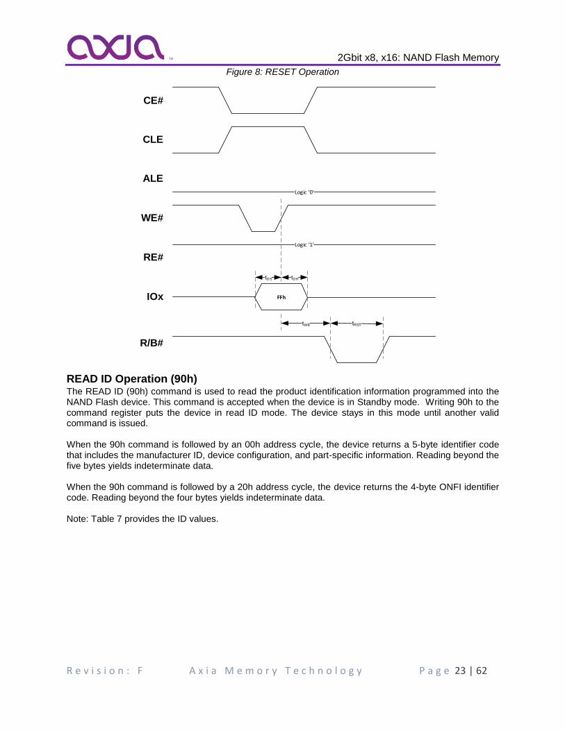
READ ID Operation (90h) The READ ID (90h) command is used to read the product identification information programmed into the NAND Flash device. This command is accepted when the device is in Standby mode. Writing 90h to the command register puts the device in read ID mode. The device stays in this mode until another valid command is issued. When the 90h command is followed by an 00h address cycle, the device returns a 5-byte identifier code that includes the manufacturer ID, device configuration, and part-specific information. Reading beyond the five bytes yields indeterminate data. When the 90h command is followed by a 20h address cycle, the device returns the 4-byte ONFI identifier code. Reading beyond the four bytes yields indeterminate data. Note: Table 7 provides the ID values.
2Gbit x8, x16: NAND Flash Memory
R e v i s i o n : F A x i a M e m o r y T e c h n o l o g y P a g e 24 | 62
Figure 9: READ ID Operation
CE#
CLE
ALE
WE#
RE#
IOx
tDHtDS
90h
tDHtDS
00h / 20h Byte 0 Byte 2 Byte 3 Byte 4
tWHR
tAR
Byte 1
READ UNIQUE ID Operation (EDh)
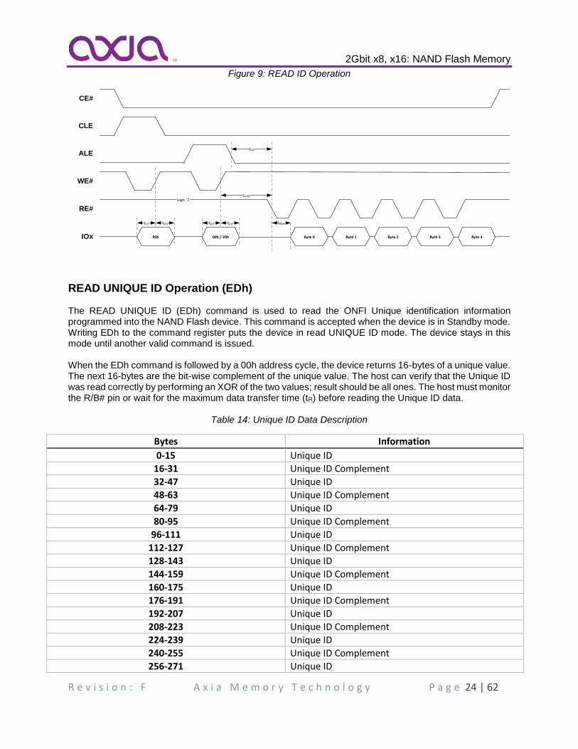
The READ UNIQUE ID (EDh) command is used to read the ONFI Unique identification information programmed into the NAND Flash device. This command is accepted when the device is in Standby mode. Writing EDh to the command register puts the device in read UNIQUE ID mode. The device stays in this mode until another valid command is issued. When the EDh command is followed by a 00h address cycle, the device returns 16-bytes of a unique value. The next 16-bytes are the bit-wise complement of the unique value. The host can verify that the Unique ID was read correctly by performing an XOR of the two values; result should be all ones. The host must monitor the R/B# pin or wait for the maximum data transfer time (tR) before reading the Unique ID data.
Table 14: Unique ID Data Description
Bytes Information
0-15 Unique ID
16-31 Unique ID Complement
32-47 Unique ID
48-63 Unique ID Complement
64-79 Unique ID
80-95 Unique ID Complement
96-111 Unique ID
112-127 Unique ID Complement
128-143 Unique ID
144-159 Unique ID Complement
160-175 Unique ID
176-191 Unique ID Complement
192-207 Unique ID
208-223 Unique ID Complement
224-239 Unique ID
240-255 Unique ID Complement
256-271 Unique ID
2Gbit x8, x16: NAND Flash Memory
R e v i s i o n : F A x i a M e m o r y T e c h n o l o g y P a g e 25 | 62
Bytes Information
272-287 Unique ID Complement
288-303 Unique ID
304-319 Unique ID Complement
320-335 Unique ID
336-351 Unique ID Complement
352-367 Unique ID
368-383 Unique ID Complement
384-399 Unique ID
400-415 Unique ID Complement
416-431 Unique ID
432-447 Unique ID Complement
448-463 Unique ID
464-479 Unique ID Complement
480-495 Unique ID
496-511 Unique ID Complement
Figure 10: READ Unique ID Operation
CE#
CLE
ALE
WE#
RE#
IOx
tDHtDS
EDh
tDHtDS
00hUnique ID
Byte 0
Unique ID
Byte 1
Unique ID
Byte 15
tR
R/B#
tWHR
tWB
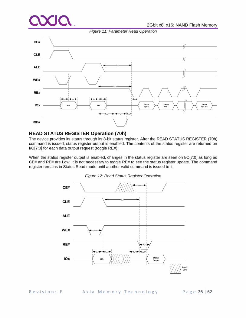
READ PARAMETER PAGE Operation (ECh) The READ PARAMETER PAGE (ECh) command is used to read the ONFI parameter page which describes the device’s organization, features, timings and other behavioral parameters. These values are static and cannot be altered by the user. The READ PARAMETER PAGE command is accepted by the device when it is in Standby mode. Writing ECh to the command register puts the device in read parameter page mode. It stays in this mode until another valid command is issued. When the ECh command is followed by an 00h address cycle, the device goes busy for tR. If desired, the RANDOM DATA OUTPUT (05h-E0h) command can be used to change the location of data output. If the READ STATUS (70h) command is used to monitor for command completion, the READ MODE (00h) command must be used to re-enable data output mode.
2Gbit x8, x16: NAND Flash Memory
R e v i s i o n : F A x i a M e m o r y T e c h n o l o g y P a g e 26 | 62
Figure 11: Parameter Read Operation
CE#
CLE
ALE
WE#
RE#
IOx
tDHtDS
ECh
tDHtDS
00hParamByte 0
ParamByte 1
ParamByte 255
tR
R/B#
READ STATUS REGISTER Operation (70h) The device provides its status through its 8-bit status register. After the READ STATUS REGISTER (70h) command is issued, status register output is enabled. The contents of the status register are returned on I/O[7:0] for each data output request (toggle RE#). When the status register output is enabled, changes in the status register are seen on I/O[7:0] as long as CE# and RE# are Low; it is not necessary to toggle RE# to see the status register update. The command register remains in Status Read mode until another valid command is issued to it.
Figure 12: Read Status Register Operation
CE#
CLE
ALE
WE#
RE#
IOx
tDHtDS
70hStatusOutput
Don tCare
tIR
tCLR
tCEA
2Gbit x8, x16: NAND Flash Memory
R e v i s i o n : F A x i a M e m o r y T e c h n o l o g y P a g e 27 | 62
READ MODE Operation (00h) Upon initial device power up, the device defaults to Read mode. This operation is also initiated by writing
00h and 30h to the command register along with four address cycles. Two types of read operations are
available: random read and serial page read. The random read mode is enabled when the page address is
changed. The repetitive high to low transitions of the RE# clock make the device output the data starting
from the selected column address up to the last column address. The device may output random data in a
page instead of the consecutive sequential data by writing random data output command. Random data
output can be operated multiple times regardless of how many times it is done in a page. Any operation
other than read or random data output causes the device to exit read mode.
The READ MODE (00h) command enables data output and disables status output after a READ operation (00h-30h, 00-31h) has been modified with a status operation (70h). This command is accepted by the device when it is ready (RDY = 1, ARDY = 1). It is also accepted by the device during READ PAGE CACHE (31h, 00h-31h) operations (RDY = 1 and ARDY = 0).
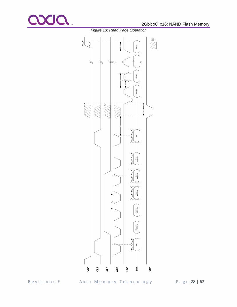
READ PAGE Operation (00h – 30h) The READ PAGE (00h–30h) command copies a page (x8: 2176 bytes, x16: 1088 words) from the NAND Flash array to its cache register and enables data output. This command is accepted by the device when it is ready (RDY = 1, ARDY = 1). To read a page from the NAND Flash array, the host must first write the 00h command to the command register, followed by writing 5 address cycles to the address registers, and conclude with writing the 30h command. The device will go busy (RDY = 0, ARDY = 0) for tR as data is transferred. To determine the progress of the data transfer, the host can monitor the device’s R/B# signal or use the READ STATUS REGISTER operation (70h). If the READ STATUS REGISTER operation is used to monitor the progress, the host must disable status output and enable data output by issuing the READ MODE (00h) command when the device gets ready (RDY = 1, ARDY = 1). As mentioned above, two types of read operations are available: random read and serial page read. During
data output the READ RANDOM DATA (05h-E0h) command can be issued if random data output from the
page is desired. Otherwise, the data output is sequential.
2Gbit x8, x16: NAND Flash Memory
R e v i s i o n : F A x i a M e m o r y T e c h n o l o g y P a g e 28 | 62
Figure 13: Read Page Operation
CE
#
CL
E
AL
E
WE
#
RE
#
IOx
t DH
t DS
00
hCo
lum
n A
dd
ress
0D
OU
T 0
DO
UT
1D
OU
T n
t Rt R
R
R/B
#
Co
lum
nA
ddre
ss 1
t DH
t DS
Ro
wA
ddre
ss 0
t DH
t DS
Ro
wA
ddre
ss 1
t DH
t DS
30
h
t WC
t WB
t RC
t WP
t RH
Z
t AR
t CLR
t CH
Z
t CO
H
Do
n t
Care
t DH
t DS
Ro
wA
ddre
ss 2
2Gbit x8, x16: NAND Flash Memory
R e v i s i o n : F A x i a M e m o r y T e c h n o l o g y P a g e 29 | 62
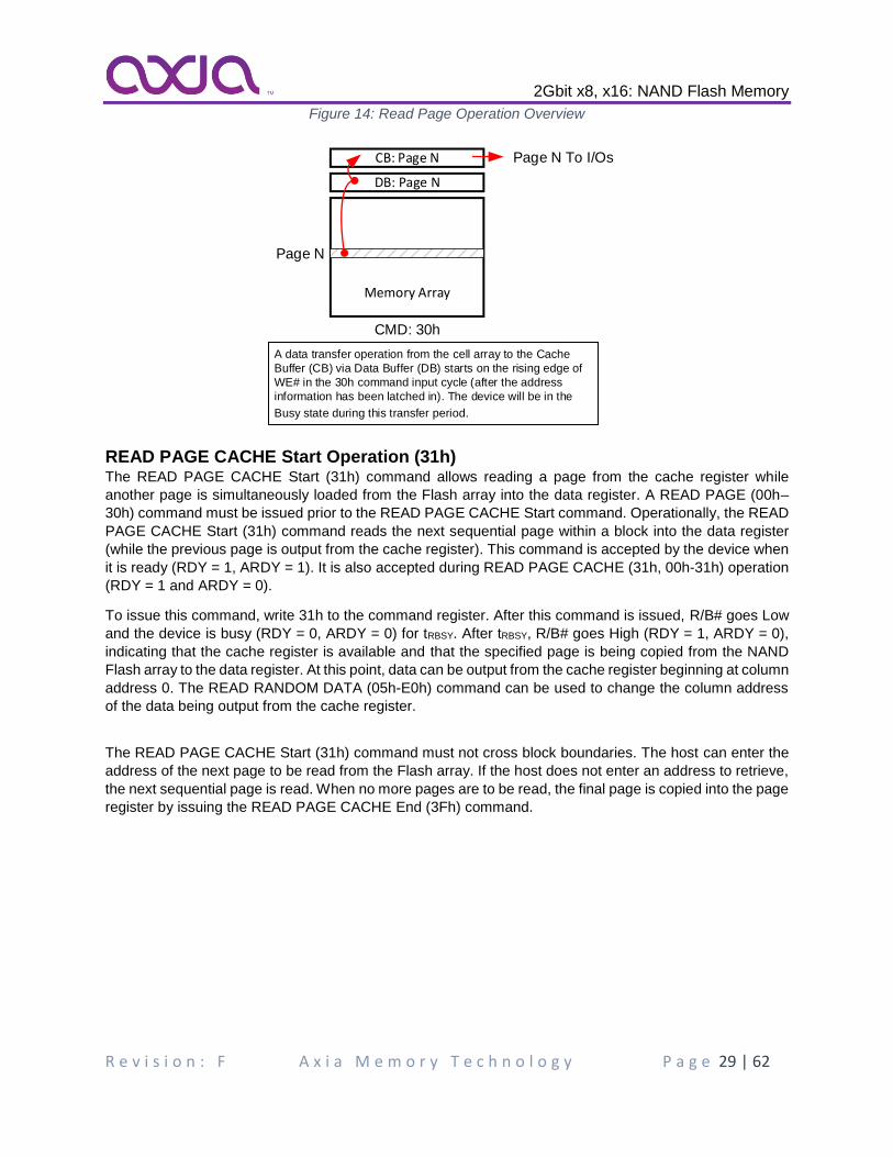
Figure 14: Read Page Operation Overview
Memory Array
DB: Page N
CB: Page N
Page N
Page N To I/Os
A data transfer operation from the cell array to the Cache
Buffer (CB) via Data Buffer (DB) starts on the rising edge of
WE# in the 30h command input cycle (after the address
information has been latched in). The device will be in the
Busy state during this transfer period.
CMD: 30h
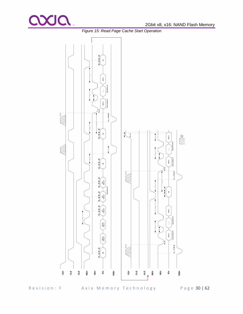
READ PAGE CACHE Start Operation (31h) The READ PAGE CACHE Start (31h) command allows reading a page from the cache register while
another page is simultaneously loaded from the Flash array into the data register. A READ PAGE (00h–
30h) command must be issued prior to the READ PAGE CACHE Start command. Operationally, the READ
PAGE CACHE Start (31h) command reads the next sequential page within a block into the data register
(while the previous page is output from the cache register). This command is accepted by the device when
it is ready (RDY = 1, ARDY = 1). It is also accepted during READ PAGE CACHE (31h, 00h-31h) operation
(RDY = 1 and ARDY = 0).
To issue this command, write 31h to the command register. After this command is issued, R/B# goes Low
and the device is busy (RDY = 0, ARDY = 0) for tRBSY. After tRBSY, R/B# goes High (RDY = 1, ARDY = 0),
indicating that the cache register is available and that the specified page is being copied from the NAND
Flash array to the data register. At this point, data can be output from the cache register beginning at column
address 0. The READ RANDOM DATA (05h-E0h) command can be used to change the column address
of the data being output from the cache register.
The READ PAGE CACHE Start (31h) command must not cross block boundaries. The host can enter the
address of the next page to be read from the Flash array. If the host does not enter an address to retrieve,
the next sequential page is read. When no more pages are to be read, the final page is copied into the page
register by issuing the READ PAGE CACHE End (3Fh) command.
2Gbit x8, x16: NAND Flash Memory
R e v i s i o n : F A x i a M e m o r y T e c h n o l o g y P a g e 30 | 62
Figure 15: Read Page Cache Start Operation
CE
#
CL
E
AL
E
WE
#
RE
#
IOx
t DH
t DS
00
hC
olu
mn
Ad
dre
ss 0
DO
UT
0
DO
UT
n
t R
R/B
#
Colu
mn
Ad
dre
ss 1
t DH
t DS
Ro
wA
dd
ress
0
t DH
t DS
Ro
wA
dd
ress
2
t DH
t DS
30
h
t WC
t WB
t RC
t WP
t RC
BS
Y
t DH
t DS
31
h
t WB
t CLR
t DH
t DS
31
h
Co
lum
n A
dd
ress
0t R
R
Pag
e A
dd
ress
MP
age
Ad
dre
ss M
t RH
W
t WH
R
t DH
t DS
Ro
wA
dd
ress
1
CE
#
CL
E
AL
E
WE
#
RE
#
IOx
DO
UT
0
DO
UT
n
R/B
#
t RC
t WP
t CH
Z
t CO
H
t RC
BS
Y
t CLR
t DH
t DS
3Fh
DO
UT
0
DO
UT
n
t RC
t WP
t RH
Z
t RC
BS
Y
t CLR
t WB
Colu
mn
Add
ress
0Co
lum
n A
ddre
ss 0
t RR
t RR
Pag
e A
dd
ress
MP
age
Ad
dre
ss M
+1
t RH
W
t WH
R
Do
n t
Car
e
2Gbit x8, x16: NAND Flash Memory
R e v i s i o n : F A x i a M e m o r y T e c h n o l o g y P a g e 31 | 62
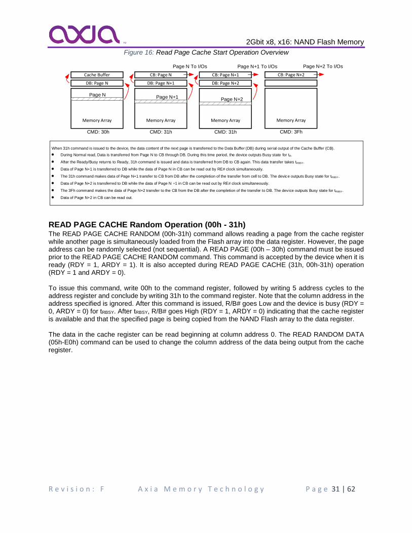
Figure 16: Read Page Cache Start Operation Overview
Memory Array
DB: Page N
Cache Buffer
Page N
Memory Array
DB: Page N+1
CB: Page N
Page N+1
Page N To I/Os
CMD: 30h CMD: 31h
Memory Array
DB: Page N+2
CB: Page N+1
Page N+2
Page N+1 To I/Os
CMD: 31h
Memory Array
CB: Page N+2
Page N+2 To I/Os
CMD: 3Fh
When 31h command is issued to the device, the data content of the next page is transferred to the Data Buffer (DB) during serial output of the Cache Buffer (CB).
• During Normal read, Data is transferred from Page N to CB through DB. During this time period, the device outputs Busy state for tR.
• After the Ready/Busy returns to Ready, 31h command is issued and data is transferred from DB to CB again. This data transfer takes tRBSY.
• Data of Page N+1 is transferred to DB while the data of Page N in CB can be read out by RE# clock simultaneously.
• The 31h command makes data of Page N+1 transfer to CB from DB after the completion of the transfer from cell to DB. The device outputs Busy state for tRBSY.
• Data of Page N+2 is transferred to DB while the data of Page N +1 in CB can be read out by RE# clock simultaneously.
• The 3Fh command makes the data of Page N+2 transfer to the CB from the DB after the completion of the transfer to DB. The device outputs Busy state for tRBSY.
• Data of Page N+2 in CB can be read out.
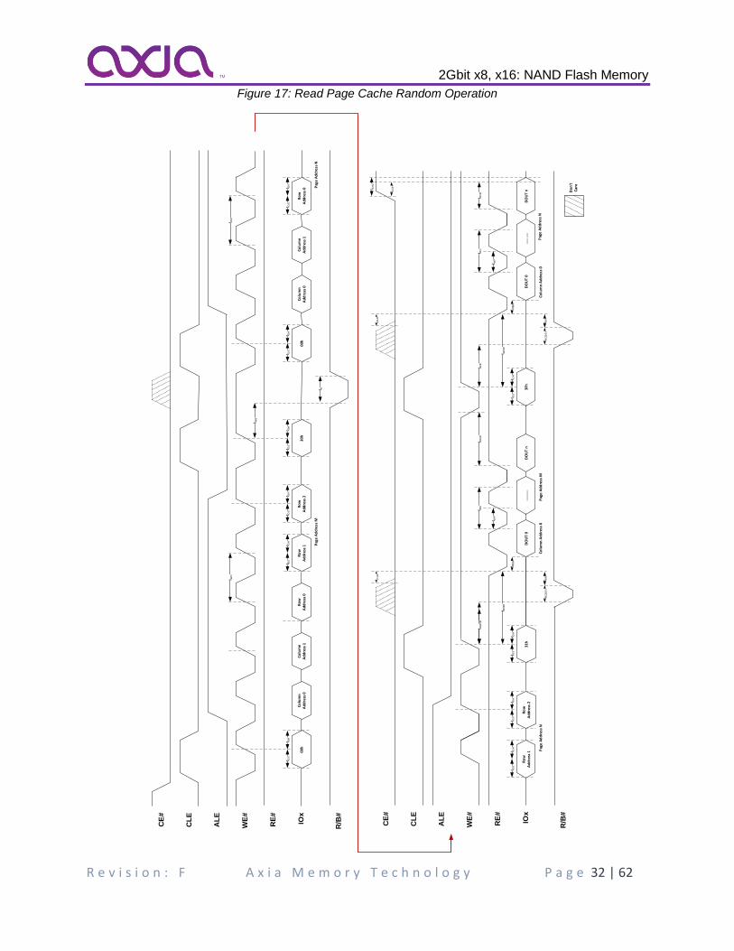
READ PAGE CACHE Random Operation (00h - 31h) The READ PAGE CACHE RANDOM (00h-31h) command allows reading a page from the cache register while another page is simultaneously loaded from the Flash array into the data register. However, the page address can be randomly selected (not sequential). A READ PAGE (00h – 30h) command must be issued prior to the READ PAGE CACHE RANDOM command. This command is accepted by the device when it is ready (RDY = 1, ARDY = 1). It is also accepted during READ PAGE CACHE (31h, 00h-31h) operation (RDY = 1 and ARDY = 0). To issue this command, write 00h to the command register, followed by writing 5 address cycles to the address register and conclude by writing 31h to the command register. Note that the column address in the address specified is ignored. After this command is issued, R/B# goes Low and the device is busy (RDY = 0, ARDY = 0) for tRBSY. After tRBSY, R/B# goes High (RDY = 1, ARDY = 0) indicating that the cache register is available and that the specified page is being copied from the NAND Flash array to the data register. The data in the cache register can be read beginning at column address 0. The READ RANDOM DATA (05h-E0h) command can be used to change the column address of the data being output from the cache register.
2Gbit x8, x16: NAND Flash Memory
R e v i s i o n : F A x i a M e m o r y T e c h n o l o g y P a g e 32 | 62
Figure 17: Read Page Cache Random Operation
CE
#
CL
E
AL
E
WE
#
RE
#
IOx
t DH
t DS
00
hC
olu
mn
Ad
dre
ss 0
t R
R/B
#
Co
lum
nA
ddre
ss 1
t DH
t DS
Ro
wA
ddre
ss 1
t DH
t DS
Ro
wA
ddre
ss 2
t DH
t DS
30
h
t WC
t WB
Pag
e A
dd
ress
M
t DH
t DS
00
hCo
lum
n A
dd
ress
0C
olu
mn
Ad
dre
ss 1
t DH
t DS
Ro
wA
dd
ress
0
t WC
Pag
e A
dd
ress
N
Ro
wA
ddre
ss 0
CE
#
CL
E
AL
E
WE
#
RE
#
IOx
DO
UT
0
DO
UT
n
R/B
#
t RC
t WP
t CH
Z
t CO
H
t RC
BS
Y
t WB
t CLR
t DH
t DS
3Fh
DO
UT
0
DO
UT
n
t RC
t WP
t RH
Z
t RC
BS
Y
t CLR
t WB
Co
lum
n A
dd
ress
0C
olu
mn
Ad
dre
ss 0
t RR
t RR
Pag
e A
dd
ress
MP
age
Ad
dre
ss N
t RH
W
t WH
Rt W
HR
t DH
t DS
Ro
wA
ddre
ss 2
t DH
t DS
31
h
t WB
Pag
e A
dd
ress
N
Do
n t
Car
e
t DH
t DS
Ro
wA
dd
ress
1
2Gbit x8, x16: NAND Flash Memory
R e v i s i o n : F A x i a M e m o r y T e c h n o l o g y P a g e 33 | 62
READ PAGE CACHE End Operation (3Fh) The READ PAGE CACHE End (3Fh) command ends the read page cache sequence and copies a page from the data register to the cache register. This command is accepted by the device when it is ready (RDY = 1, ARDY = 1). It is also accepted by the die (LUN) during READ PAGE CACHE (31h, 00h-31h) operations (RDY = 1 and ARDY = 0). To issue the READ PAGE CACHE End (3Fh) command, write 3Fh to the command register. After this command is issued, R/B# goes LOW and device is busy (RDY = 0, ARDY = 0) for tRBSY. After tRBSY, R/B# goes HIGH and the device is ready (RDY = 1, ARDY = 1). At this point, data can be output from the cache register, beginning at column address 0. The READ RANDOM DATA (05h-E0h) command can be used to change the column address of the data being output from the cache register.
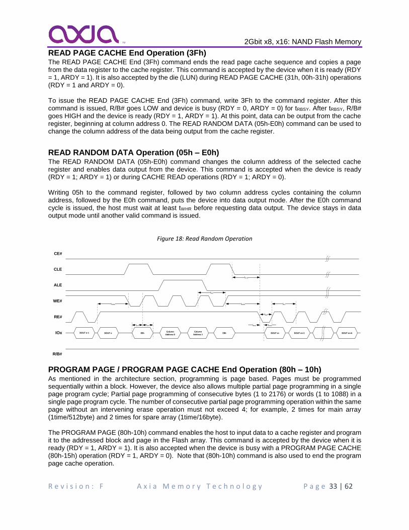
READ RANDOM DATA Operation (05h – E0h) The READ RANDOM DATA (05h-E0h) command changes the column address of the selected cache register and enables data output from the device. This command is accepted when the device is ready (RDY = 1; ARDY = 1) or during CACHE READ operations (RDY = 1; ARDY = 0). Writing 05h to the command register, followed by two column address cycles containing the column address, followed by the E0h command, puts the device into data output mode. After the E0h command cycle is issued, the host must wait at least tWHR before requesting data output. The device stays in data output mode until another valid command is issued.
Figure 18: Read Random Operation
CE#
CLE
ALE
WE#
RE#
IOx DOUT n
R/B#
tDHtDS
05hColumn
Address 0Column
Address 1
tWC
E0h DOUT m DOUT m+1 DOUT m+k
tRC
tWP
DOUT n-1
tRHW tWHR
tCLR
tREA tREA
PROGRAM PAGE / PROGRAM PAGE CACHE End Operation (80h – 10h) As mentioned in the architecture section, programming is page based. Pages must be programmed sequentially within a block. However, the device also allows multiple partial page programming in a single page program cycle; Partial page programming of consecutive bytes (1 to 2176) or words (1 to 1088) in a single page program cycle. The number of consecutive partial page programming operation within the same page without an intervening erase operation must not exceed 4; for example, 2 times for main array (1time/512byte) and 2 times for spare array (1time/16byte). The PROGRAM PAGE (80h-10h) command enables the host to input data to a cache register and program it to the addressed block and page in the Flash array. This command is accepted by the device when it is ready (RDY = 1, ARDY = 1). It is also accepted when the device is busy with a PROGRAM PAGE CACHE (80h-15h) operation (RDY = 1, ARDY = 0). Note that (80h-10h) command is also used to end the program page cache operation.
2Gbit x8, x16: NAND Flash Memory
R e v i s i o n : F A x i a M e m o r y T e c h n o l o g y P a g e 34 | 62
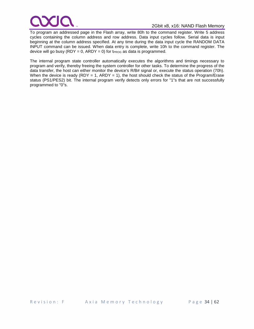
To program an addressed page in the Flash array, write 80h to the command register. Write 5 address cycles containing the column address and row address. Data input cycles follow. Serial data is input beginning at the column address specified. At any time during the data input cycle the RANDOM DATA INPUT command can be issued. When data entry is complete, write 10h to the command register. The device will go busy (RDY = 0, ARDY = 0) for tPROG as data is programmed. The internal program state controller automatically executes the algorithms and timings necessary to program and verify, thereby freeing the system controller for other tasks. To determine the progress of the data transfer, the host can either monitor the device's R/B# signal or, execute the status operation (70h). When the device is ready (RDY = 1, ARDY = 1), the host should check the status of the Program/Erase status (PS1/PES2) bit. The internal program verify detects only errors for "1"s that are not successfully programmed to "0"s.

2Gbit x8, x16: NAND Flash Memory
R e v i s i o n : F A x i a M e m o r y T e c h n o l o g y P a g e 35 | 62
Figure 19: Program Page Operation C
E#
CL
E
AL
E
WE
#
RE
#
IOx
t DH
t DS
80
hC
olu
mn
Ad
dre
ss 0
DIN
0
R/B
#
Co
lum
nA
dd
ress
1
t DH
t DS
Ro
wA
dd
ress
1
t DH
t DS
Ro
wA
dd
ress
2
t WC
t DH
t DS
t AD
L
t DH
t DS
Ro
wA
dd
ress
0
CE
#
CL
E
AL
E
WE
#
RE
#
IOx
t PR
OG
R/B
#
t CO
H
DIN
m1
0h
70
hSt
atu
sO
utp
ut
t DH
t DS
Do
n t
Care
t RE
A
2Gbit x8, x16: NAND Flash Memory
R e v i s i o n : F A x i a M e m o r y T e c h n o l o g y P a g e 36 | 62
Figure 20: Program Page Operation Overview
Memory Array
DB: Data Input
CB: Data Input
Selected Page
Data Input From I/Os
The data is programmed from the Data Buffer (DB) to the
selected page on the rising edge of WE# following input of the
h command. After programming, the programmed data is
transferred back to the DB to be automatically verified by the
device. If the programming does not succeed, the Program/
Verify operation is repeated by the device until success is
achieved or until the maximum programming loop count is
reached.
CMD: 10h
Program / Read / Verify
PROGRAM PAGE CACHE Operation (80h – 15h) PROGRAM PAGE CACHE is used to improve the program throughput by programing data using the cache register. Cache program is available only within a block. The PROGRAM PAGE CACHE (80h-15h) command is an extension of the PROGRAM PAGE (80h-10h) command. The PROGRAM PAGE CACHE (80h-15h) command enables the host to input data to the cache register while the data register contents are programmed to the memory array. The PROGRAM PAGE CACHE command is accepted by the device when it is ready (RDY =1, ARDY = 1). It is also accepted by the device when it is busy with a PROGRAM PAGE CACHE operation (RDY = 1, ARDY = 0). To input a page to the cache register, write 80h to the command register. Then write 5 address cycles containing the column address and row address. Data input cycles follow. Serial data is input beginning at the column address specified. At any time during the data input cycle the RANDOM DATA INPUT (85h) command can be issued. When data input is complete, write 15h to the command register. The device will go busy (RDY = 0, ARDY = 0) for tPBSY to copy data from the cache register to the data register, and then to begin the programming operation. To determine the progress of the data transfer, the host can either monitor the device's R/B# signal or, execute the READ STATUS REGISTER (70h) command. When the device is busy with a PROGRAM PAGE CACHE operation (RDY = 1, ARDY = 0), the host must check the status of the PS1 bit to ensure cache operation was successful. If, after tPBSY, the host wants to wait for the program cache operation to complete without issuing PROGRAM PAGE (80h-10h) command, the host should monitor ARDY bit in the status register until it is 1. The host should then check the status of the PS1 and PES2 bits for program completion status.
2Gbit x8, x16: NAND Flash Memory
R e v i s i o n : F A x i a M e m o r y T e c h n o l o g y P a g e 37 | 62
Figure 21: Page Cache Program Operation
CE
#
CL
E
AL
E
WE
#
RE
#
IOx
t DH
t DS
80
hC
olu
mn
Ad
dre
ss 0
DIN
0
t CB
SY
R/B
#
Co
lum
nA
ddre
ss 1
t DH
t DS
Ro
wA
ddre
ss 1
t DH
t DS
Ro
wA
ddre
ss 2
t WC
DIN
m1
5h
t DH
t DS
t DH
t DS
t AD
L
t DH
t DS
80
hC
olu
mn
Ad
dre
ss 0
Pag
e A
dd
ress
M
Ro
wA
ddre
ss 0
CE
#
CL
E
AL
E
WE
#
RE
#
IOx
R/B
#
t CH
Z
t CO
H
70
hSt
atus
Ou
tpu
t
Do
n t
Care
t RE
A
Co
lum
n A
dd
ress
0D
IN 0
t PR
OG
Colu
mn
Ad
dre
ss 1
t DH
t DS
Ro
wA
dd
ress
1
t DH
t DS
Ro
wA
dd
ress
2
t WC
DIN
m1
0h
t DH
t DS
t DH
t DS
t AD
L
Pag
e A
dd
ress
N
Ro
wA
dd
ress
0
2Gbit x8, x16: NAND Flash Memory
R e v i s i o n : F A x i a M e m o r y T e c h n o l o g y P a g e 38 | 62
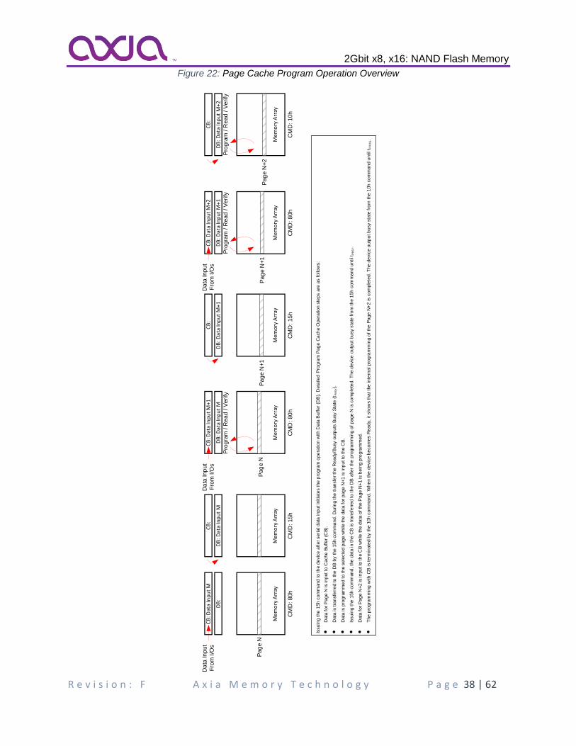
Figure 22: Page Cache Program Operation Overview
Mem
ory
Arr
ayM
emo
ry A
rray
DB
:
CB
: Dat
a In
put
M
Pag
e N
Da
ta Inp
ut
Fro
m I/O
s
CM
D: 80h
Mem
ory
Arr
ay
DB
: Dat
a In
put
M
CB
:
CM
D: 15h
Mem
ory
Arr
ay
DB
: Dat
a In
put
M
CB
: Dat
a In
put
M+1
Da
ta Inp
ut
Fro
m I/O
s
CM
D: 80h
Mem
ory
Arr
ay
DB
: Dat
a In
put
M+1
CB
:
CM
D: 15h
Pro
gra
m / R
ead / V
erify
Pro
gra
m / R
ead / V
erify
Pag
e N
+1
Mem
ory
Arr
ay
DB
: Dat
a In
put
M+2
CB
:
CM
D: 10h
Pro
gra
m / R
ead / V
erify
Pag
e N
+2
Pag
e N
DB
: Dat
a In
put
M+1
CB
: Dat
a In
put
M+2
Da
ta Inp
ut
Fro
m I/O
s
CM
D: 80h
Pag
e N
+1
Issu
ing
the
15
h c
om
man
d t
o t
he
de
vic
e a
fte
r se
ria
l d
ata
in
pu
t in
itia
tes t
he
pro
gra
m o
pe
ratio
n w
ith
Da
ta B
uff
er
(DB
). D
eta
iled
Pro
gra
m P
ag
e C
ach
e O
pe
ratio
n s
tep
s a
re a
s f
ollo
ws:
•
Data
fo
r P
ag
e N
is in
put
to C
ache
Bu
ffe
r (C
B).
•
Data
is t
ran
sfe
rre
d to
th
e D
B b
y t
he
15
h c
om
ma
nd
. D
uri
ng
the
tra
nsfe
r th
e R
ea
dy/B
usy o
utp
uts
Bu
sy S
tate
(t P
BS
Y).
•
Data
is p
rog
ram
me
d t
o t
he s
ele
cte
d p
ag
e w
hile t
he
da
ta f
or
pa
ge
N+
1 is in
pu
t to
th
e C
B.
•
Issu
ing
the
15
h c
om
man
d,
the
da
ta in
th
e C
B is t
ran
sfe
rre
d t
o t
he D
B a
fte
r th
e p
rog
ram
min
g o
f p
ag
e N
is c
om
ple
ted
. T
he
de
vic
e o
utp
ut
bu
sy s
tate
fro
m t
he
15
h c
om
ma
nd
un
til t P
BS
Y.
•
Data
fo
r P
ag
e N
+2
is in
pu
t to
th
e C
B w
hile
th
e d
ata
of
the
Pa
ge
N+
1 is b
ein
g p
rog
ram
me
d.
•
Th
e p
rog
ram
min
g w
ith
CB
is t
erm
ina
ted
by t
he
10
h c
om
ma
nd
. W
he
n t
he
de
vic
e b
eco
me
s R
ea
dy,
it s
ho
ws th
at
the
in
tern
al p
rog
ram
min
g o
f th
e P
ag
e N
+2
is c
om
ple
ted
. T
he
de
vic
e o
utp
ut
bu
sy s
tate
fro
m t
he
10h
co
mm
an
d u
ntil t P
RO
G.
2Gbit x8, x16: NAND Flash Memory
R e v i s i o n : F A x i a M e m o r y T e c h n o l o g y P a g e 39 | 62
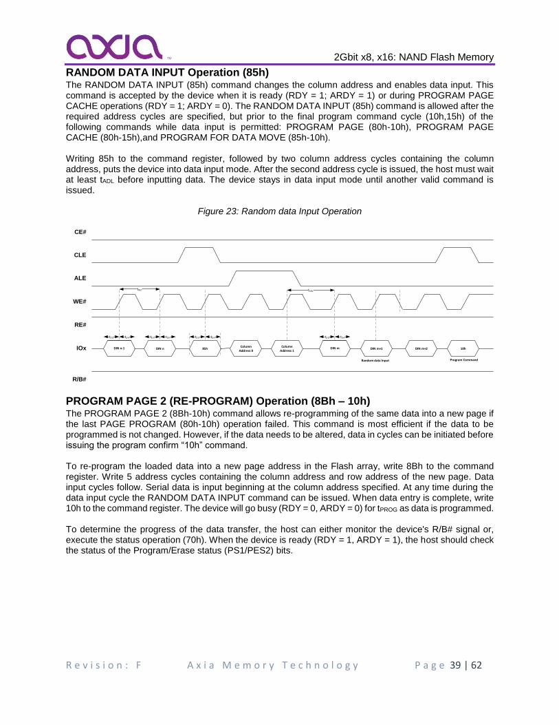
RANDOM DATA INPUT Operation (85h) The RANDOM DATA INPUT (85h) command changes the column address and enables data input. This command is accepted by the device when it is ready (RDY = 1; ARDY = 1) or during PROGRAM PAGE CACHE operations (RDY = 1; ARDY = 0). The RANDOM DATA INPUT (85h) command is allowed after the required address cycles are specified, but prior to the final program command cycle (10h,15h) of the following commands while data input is permitted: PROGRAM PAGE (80h-10h), PROGRAM PAGE CACHE (80h-15h),and PROGRAM FOR DATA MOVE (85h-10h). Writing 85h to the command register, followed by two column address cycles containing the column address, puts the device into data input mode. After the second address cycle is issued, the host must wait at least tADL before inputting data. The device stays in data input mode until another valid command is issued.
Figure 23: Random data Input Operation
CE#
CLE
ALE
WE#
RE#
IOx DIN n
R/B#
tDHtDS
85hColumn
Address 0Column
Address 1
tWC
10hDIN n-1
tDHtDS
DIN m+1DIN m
tDHtDS
DIN m+2
tDHtDS
tADL
Random data Input Program Command
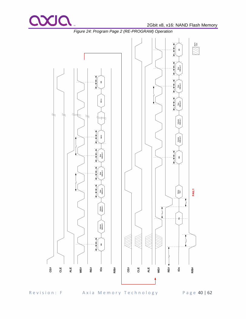
PROGRAM PAGE 2 (RE-PROGRAM) Operation (8Bh – 10h) The PROGRAM PAGE 2 (8Bh-10h) command allows re-programming of the same data into a new page if the last PAGE PROGRAM (80h-10h) operation failed. This command is most efficient if the data to be programmed is not changed. However, if the data needs to be altered, data in cycles can be initiated before issuing the program confirm “10h” command. To re-program the loaded data into a new page address in the Flash array, write 8Bh to the command register. Write 5 address cycles containing the column address and row address of the new page. Data input cycles follow. Serial data is input beginning at the column address specified. At any time during the data input cycle the RANDOM DATA INPUT command can be issued. When data entry is complete, write 10h to the command register. The device will go busy (RDY = 0, ARDY = 0) for tPROG as data is programmed. To determine the progress of the data transfer, the host can either monitor the device's R/B# signal or, execute the status operation (70h). When the device is ready (RDY = 1, ARDY = 1), the host should check the status of the Program/Erase status (PS1/PES2) bits.
2Gbit x8, x16: NAND Flash Memory
R e v i s i o n : F A x i a M e m o r y T e c h n o l o g y P a g e 40 | 62
Figure 24: Program Page 2 (RE-PROGRAM) Operation
CE
#
CL
E
AL
E
WE
#
RE
#
IOx
t DH
t DS
80
hC
olu
mn
Ad
dre
ss 0
DIN
0
R/B
#
Colu
mn
Ad
dre
ss 1
t DH
t DS
Ro
wA
dd
ress
1
t DH
t DS
Ro
wA
dd
ress
2
t WC
t DH
t DS
t AD
L
t DH
t DS
Ro
wA
dd
ress
0
CE
#
CL
E
AL
E
WE
#
RE
#
IOx
t PR
OG
R/B
#
70
hSt
atu
s E
1h
Do
n t
Car
e
t RE
A
t DH
t DS
8B
hC
olu
mn
Ad
dre
ss 0
Co
lum
nA
dd
ress
1
t DH
t DS
Ro
wA
dd
ress
1
t DH
t DS
Ro
wA
dd
ress
2
t WC
t DH
t DS
Ro
wA
dd
ress
0
t DH
t DS
10h
FA
IL!!
DIN
m1
0h
t DH
t DS
2Gbit x8, x16: NAND Flash Memory
R e v i s i o n : F A x i a M e m o r y T e c h n o l o g y P a g e 41 | 62
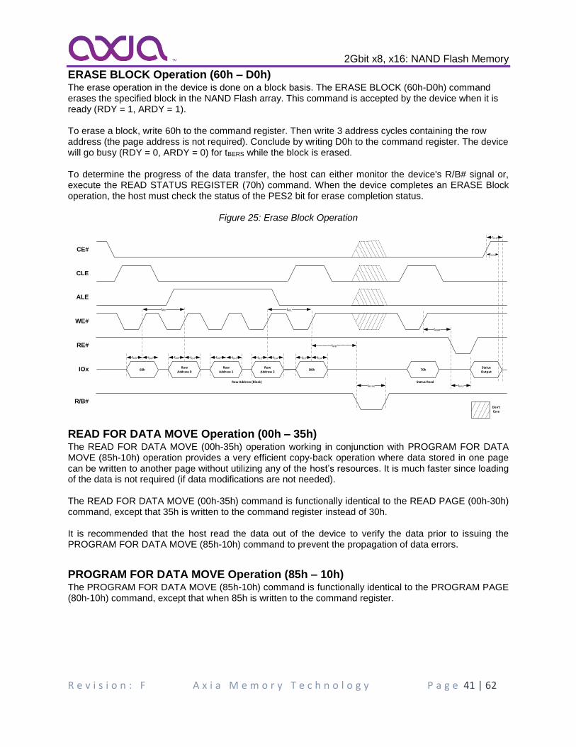
ERASE BLOCK Operation (60h – D0h) The erase operation in the device is done on a block basis. The ERASE BLOCK (60h-D0h) command erases the specified block in the NAND Flash array. This command is accepted by the device when it is ready (RDY = 1, ARDY = 1). To erase a block, write 60h to the command register. Then write 3 address cycles containing the row address (the page address is not required). Conclude by writing D0h to the command register. The device will go busy (RDY = 0, ARDY = 0) for tBERS while the block is erased. To determine the progress of the data transfer, the host can either monitor the device's R/B# signal or, execute the READ STATUS REGISTER (70h) command. When the device completes an ERASE Block operation, the host must check the status of the PES2 bit for erase completion status.
Figure 25: Erase Block Operation
CE#
CLE
ALE
WE#
RE#
IOx
tDH
60h
tBERS
R/B#
tDH
RowAddress 0
tDHtDS
RowAddress 2
tCHZ
tCOH
D0h 70hStatusOutput
tDHtDS
tADL
Don tCare
tREA
Row Address (Block) Status Read
tDH
RowAddress 1
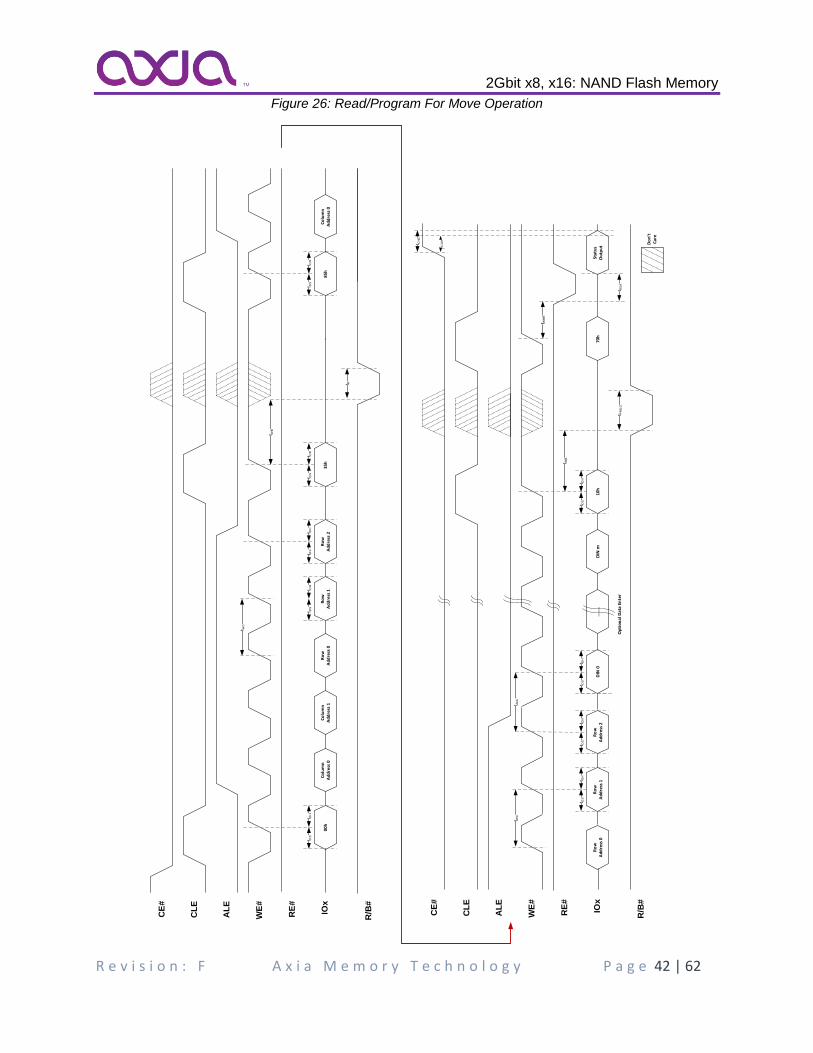
READ FOR DATA MOVE Operation (00h – 35h) The READ FOR DATA MOVE (00h-35h) operation working in conjunction with PROGRAM FOR DATA MOVE (85h-10h) operation provides a very efficient copy-back operation where data stored in one page can be written to another page without utilizing any of the host’s resources. It is much faster since loading of the data is not required (if data modifications are not needed). The READ FOR DATA MOVE (00h-35h) command is functionally identical to the READ PAGE (00h-30h) command, except that 35h is written to the command register instead of 30h. It is recommended that the host read the data out of the device to verify the data prior to issuing the PROGRAM FOR DATA MOVE (85h-10h) command to prevent the propagation of data errors.
PROGRAM FOR DATA MOVE Operation (85h – 10h) The PROGRAM FOR DATA MOVE (85h-10h) command is functionally identical to the PROGRAM PAGE (80h-10h) command, except that when 85h is written to the command register.
2Gbit x8, x16: NAND Flash Memory
R e v i s i o n : F A x i a M e m o r y T e c h n o l o g y P a g e 42 | 62
Figure 26: Read/Program For Move Operation
CE
#
CL
E
AL
E
WE
#
RE
#
IOx
t DH
t DS
00
hC
olu
mn
Ad
dre
ss 0
t R
R/B
#
Co
lum
nA
dd
ress
1
t DH
t DS
Ro
wA
dd
ress
1
t DH
t DS
Ro
wA
dd
ress
2
t DH
t DS
35
h
t WC
t WB
t DH
t DS
85
hC
olu
mn
Ad
dre
ss 0
Ro
wA
dd
ress
0
CE
#
CL
E
AL
E
WE
#
RE
#
IOx
R/B
#
DIN
0
t PR
OG
t DH
t DS
Ro
wA
dd
ress
1
t DH
t DS
Ro
wA
dd
ress
2
t WC
t CH
Z
t CO
H
DIN
m1
0h
70
hSt
atu
sO
utp
ut
t DH
t DS
t DH
t DS
t AD
L
Do
n t
Car
e
t RE
AO
pti
on
al D
ata
Ente
r
Ro
wA
dd
ress
0
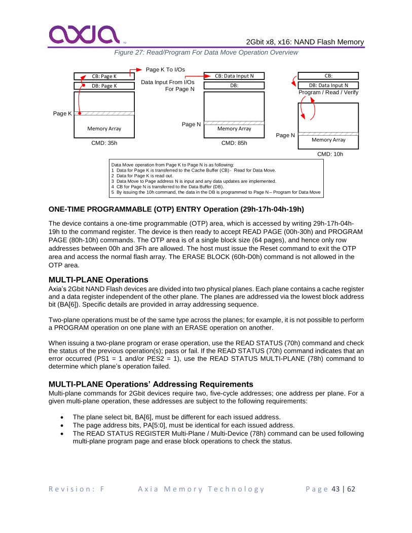
2Gbit x8, x16: NAND Flash Memory
R e v i s i o n : F A x i a M e m o r y T e c h n o l o g y P a g e 43 | 62
Figure 27: Read/Program For Data Move Operation Overview
Memory Array
DB: Page K
CB: Page K
Page K
Page K To I/Os
CMD: 35h
Memory Array
DB:
CB: Data Input NData Input From I/Os
For Page N
CMD: 85h
Page N
Memory Array
DB: Data Input N
CB:
CMD: 10h
Program / Read / Verify
Page N
Data Move operation from Page K to Page N is as following:
1 Data for Page K is transferred to the Cache Buffer (CB) - Read for Data Move.
2 Data for Page K is read out.
3 Data Move to Page address N is input and any data updates are implemented.
4 CB for Page N is transferred to the Data Buffer (DB).
5 By issuing the 10h command, the data in the DB is programmed to Page N – Program for Data Move
ONE-TIME PROGRAMMABLE (OTP) ENTRY Operation (29h-17h-04h-19h)
The device contains a one-time programmable (OTP) area, which is accessed by writing 29h-17h-04h-
19h to the command register. The device is then ready to accept READ PAGE (00h-30h) and PROGRAM
PAGE (80h-10h) commands. The OTP area is of a single block size (64 pages), and hence only row
addresses between 00h and 3Fh are allowed. The host must issue the Reset command to exit the OTP
area and access the normal flash array. The ERASE BLOCK (60h-D0h) command is not allowed in the
OTP area.
MULTI-PLANE Operations Axia’s 2Gbit NAND Flash devices are divided into two physical planes. Each plane contains a cache register and a data register independent of the other plane. The planes are addressed via the lowest block address bit (BA[6]). Specific details are provided in array addressing sequence. Two-plane operations must be of the same type across the planes; for example, it is not possible to perform a PROGRAM operation on one plane with an ERASE operation on another. When issuing a two-plane program or erase operation, use the READ STATUS (70h) command and check the status of the previous operation(s); pass or fail. If the READ STATUS (70h) command indicates that an error occurred (PS1 = 1 and/or PES2 = 1), use the READ STATUS MULTI-PLANE (78h) command to determine which plane’s operation failed.
MULTI-PLANE Operations’ Addressing Requirements Multi-plane commands for 2Gbit devices require two, five-cycle addresses; one address per plane. For a given multi-plane operation, these addresses are subject to the following requirements:
• The plane select bit, BA[6], must be different for each issued address.
• The page address bits, PA[5:0], must be identical for each issued address.
• The READ STATUS REGISTER Multi-Plane / Multi-Device (78h) command can be used following multi-plane program page and erase block operations to check the status.
2Gbit x8, x16: NAND Flash Memory
R e v i s i o n : F A x i a M e m o r y T e c h n o l o g y P a g e 44 | 62
PROGRAM PAGE MP Operation
(80h – 11h – 81h – 10h) / (80h – 11h – 80h – 10h) The PROGRAM PAGE MP (80h-11h-81h/80h-10h) command enables the host to program two pages in parallel (one in each plane). A multi-plane program cycle consists of a double serial data loading period in which up to 4352 bytes of data can be loaded into the data register, followed by a non-volatile programming period where the loaded data is programmed into the appropriate cells. Two command sequences are shown which realize the same operation. To input a page to the cache register and queue it to be moved to the NAND Flash array at the specified address, write 80h to the command register followed by five address cycles containing the column address and row address. Data input cycles follow where serial data is input beginning at the specified address. At any time during the data input cycle, the RANDOM DATA INPUT (85h) command can be issued. When data input is complete, write 11h to the command register. The device will go busy (RDY = 0, ARDY = 0) for tPBSY. To determine the progress of tPBSY, the host can monitor the devices R/B# signal or, issue the READ STATUS REGISTER operations (70h, 78h). When the device’s status shows that it is ready (RDY = 1), additional PROGRAM PAGE MP (80h-11h) commands can be issued to queue additional planes for data transfer. Alternatively, the PROGRAM PAGE (80h-10h) or PROGRAM PAGE CACHE (80h-15h) commands can be issued. When the PROGRAM PAGE (80h-10h) command is used as the final command of a multi-plane program operation, data is transferred from the cache registers to the NAND Flash array for all addressed planes during tPROG. When the device is ready (RDY = 1, ARDY = 1), the host should check the status of the PS1/PES2 bits for each of the planes to verify that programming was successfully. Note that all commands are prohibited between 11h and 81h/80h except for READ STATUS REGISTER /
READ STATUS REGISTER MP/MD and RESET commands.
Note that the PROGRAM PAGE MP command is available only within two paired blocks in separate planes. This is accomplished in two ways:
1. (80h – 11h – 81h – 10h) - By setting the block address bits for the first plane to all zeros and the second address issued selects the block for both planes (plane address bit must be ‘1’ in the second address issued).
2. (80h – 11h – 80h – 10h) - Both addresses are issued in this protocol, however, the block address bits must be the same except for the bit(s) that select the planes.
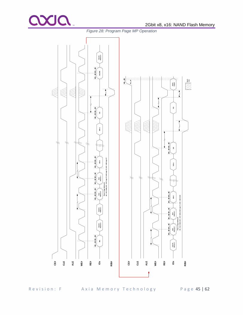
2Gbit x8, x16: NAND Flash Memory
R e v i s i o n : F A x i a M e m o r y T e c h n o l o g y P a g e 45 | 62
Figure 28: Program Page MP Operation
CE
#
CL
E
AL
E
WE
#
RE
#
IOx
t DH
t DS
80h
Co
lum
n A
dd
ress
0D
IN 0
t DB
SY
R/B
#
Co
lum
nA
ddre
ss 1
t DH
t DS
Ro
wA
ddre
ss 0
t DH
t DS
Ro
wA
ddre
ss 1
t WC
DIN
m11
h
t DH
t DS
t DH
t DS
t AD
L
t DH
t DS 81
h/8
0hC
olu
mn
Ad
dre
ss 0
Pla
ne
1, P
age
Ad
dre
ss M
CE
#
CL
E
AL
E
WE
#
RE
#
IOx
R/B
#
t CH
Z
t CO
H
70
hSt
atu
sO
utp
ut
Do
n t
Car
e
t RE
A
DIN
0
t PR
OG
Co
lum
nA
dd
ress
1
t DH
t DS
Ro
wA
dd
ress
0
t DH
t DS
Ro
wA
dd
ress
1
t WC
DIN
m1
0h
t DH
t DS
t DH
t DS
t AD
L
Pla
ne
2, P
age
Ad
dre
ss N
A0
– A
11
: Val
id, A
12
– A
17
: Lo
gic
A1
8: L
ogi
c
A1
9 –
A2
8: L
ogi
c
A0
– A
11: V
alid
, A12
– A
17: V
alid
, A18
: Lo
gic
A19
– A
28: V
alid
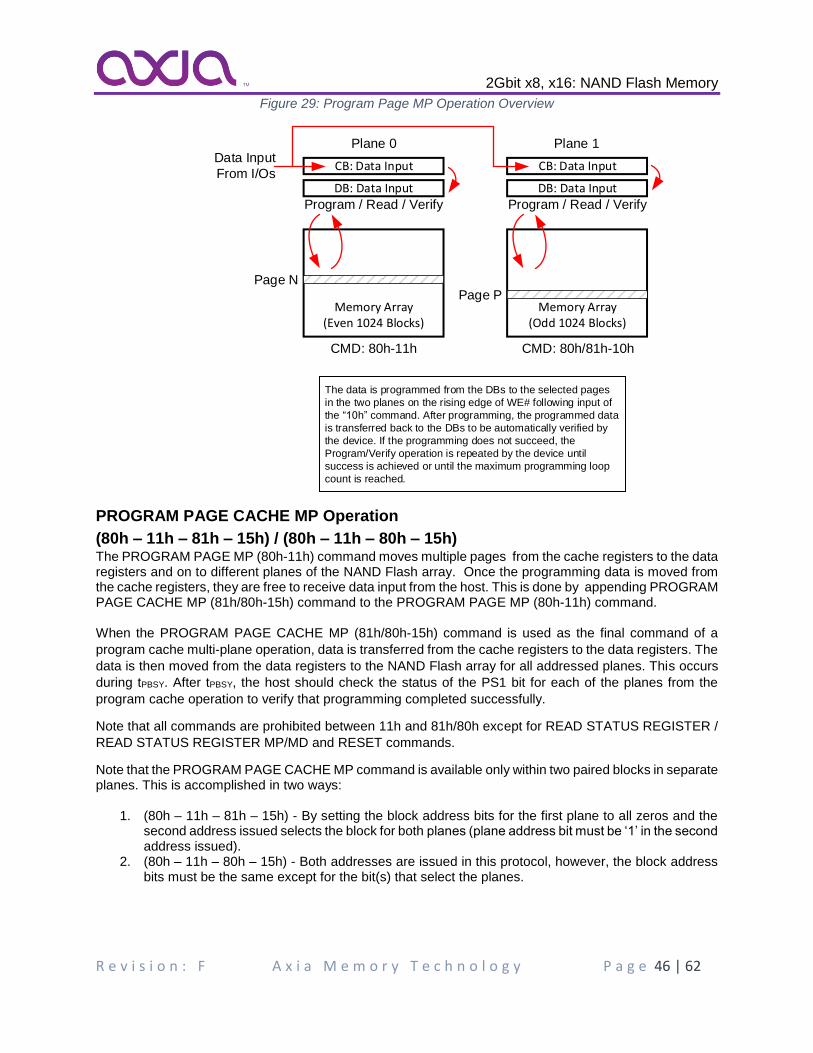
2Gbit x8, x16: NAND Flash Memory
R e v i s i o n : F A x i a M e m o r y T e c h n o l o g y P a g e 46 | 62
Figure 29: Program Page MP Operation Overview
Memory Array(Even 1024 Blocks)
DB: Data Input
CB: Data Input
Page N
Data Input
From I/Os
The data is programmed from the DBs to the selected pages
in the two planes on the rising edge of WE# following input of
the h command. After programming, the programmed data
is transferred back to the DBs to be automatically verified by
the device. If the programming does not succeed, the
Program/Verify operation is repeated by the device until
success is achieved or until the maximum programming loop
count is reached.
CMD: 80h-11h
Program / Read / Verify
Memory Array(Odd 1024 Blocks)
DB: Data Input
CB: Data Input
Page P
CMD: 80h/81h-10h
Program / Read / Verify
Plane 0 Plane 1
PROGRAM PAGE CACHE MP Operation
(80h – 11h – 81h – 15h) / (80h – 11h – 80h – 15h) The PROGRAM PAGE MP (80h-11h) command moves multiple pages from the cache registers to the data registers and on to different planes of the NAND Flash array. Once the programming data is moved from the cache registers, they are free to receive data input from the host. This is done by appending PROGRAM PAGE CACHE MP (81h/80h-15h) command to the PROGRAM PAGE MP (80h-11h) command. When the PROGRAM PAGE CACHE MP (81h/80h-15h) command is used as the final command of a
program cache multi-plane operation, data is transferred from the cache registers to the data registers. The
data is then moved from the data registers to the NAND Flash array for all addressed planes. This occurs
during tPBSY. After tPBSY, the host should check the status of the PS1 bit for each of the planes from the
program cache operation to verify that programming completed successfully.
Note that all commands are prohibited between 11h and 81h/80h except for READ STATUS REGISTER /
READ STATUS REGISTER MP/MD and RESET commands.
Note that the PROGRAM PAGE CACHE MP command is available only within two paired blocks in separate planes. This is accomplished in two ways:
1. (80h – 11h – 81h – 15h) - By setting the block address bits for the first plane to all zeros and the second address issued selects the block for both planes (plane address bit must be ‘1’ in the second address issued).
2. (80h – 11h – 80h – 15h) - Both addresses are issued in this protocol, however, the block address bits must be the same except for the bit(s) that select the planes.
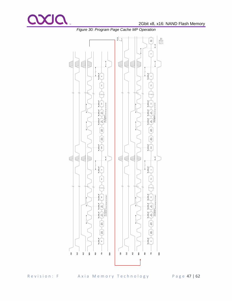
2Gbit x8, x16: NAND Flash Memory
R e v i s i o n : F A x i a M e m o r y T e c h n o l o g y P a g e 47 | 62
Figure 30: Program Page Cache MP Operation
CE
#
CL
E
AL
E
WE
#
RE
#
IOx
t DH
t DS
80h
Colu
mn
Add
ress
0D
IN 0
t DB
SY
R/B
#
Colu
mn
Add
ress
1
t DH
t DS
Row
Add
ress
0
t DH
t DS
Row
Add
ress
1
t WC
DIN
m11
h
t DH
t DS
t DH
t DS
t AD
L
t DH
t DS 81
h/80
hCo
lum
n A
ddre
ss 0
DIN
0
t DB
SY
Colu
mn
Add
ress
1
t DH
t DS
Row
Add
ress
0
t DH
t DS
Row
Add
ress
1
t WC
DIN
m15
h
t DH
t DS
t DH
t DS
t AD
L
Plan
e 1,
Pag
e A
ddre
ss M
Plan
e 1,
Pag
e A
ddre
ss N
CE
#
CL
E
AL
E
WE
#
RE
#
IOx
t DH
t DS
80h
Colu
mn
Add
ress
0D
IN 0
t DB
SY
R/B
#
Colu
mn
Add
ress
1
t DH
t DS
Row
Add
ress
0
t DH
t DS
Row
Add
ress
1
t WC
t CH
Z
t CO
H
DIN
m11
h70
hSt
atus
Out
put
t DH
t DS
t DH
t DS
t AD
L
Don
tCa
re
t RE
A
t DH
t DS 81
h/80
hCo
lum
n A
ddre
ss 0
DIN
0
t PR
OG
Colu
mn
Add
ress
1
t DH
t DS
Row
Add
ress
0
t DH
t DS
Row
Add
ress
1
t WC
DIN
m10
h
t DH
t DS
t DH
t DS
t AD
L
Plan
e 2,
Pag
e A
ddre
ss O
Plan
e 2,
Pag
e A
ddre
ss P
A0
– A
11: V
alid
, A12
– A
17: L
ogic
A18
: Log
ic
A19
– A
28: L
ogic
A0
– A
11: V
alid
, A12
– A
17: V
alid
, A18
: Log
ic
A19
– A
28: V
alid
A0
– A
11: V
alid
, A12
– A
17: L
ogic
A18
: Log
ic
A19
– A
28: L
ogic
A0
– A
11: V
alid
, A12
– A
17: V
alid
, A18
: Log
ic
A19
– A
28: V
alid
2Gbit x8, x16: NAND Flash Memory
R e v i s i o n : F A x i a M e m o r y T e c h n o l o g y P a g e 48 | 62
ERASE BLOCK MP Operation
(60h – 60h – D0h) / (60h – D1h – 60h – D0h) The ERASE BLOCK MP (60h-D1h or 60h) command queues a plane addressed block to be erased in the NAND Flash array. This command can be issued one or more times. Each time a new plane address is specified, that block in the plane is queued to be erased. To specify the final block to be erased and to begin the ERASE operation for all previously queued planes, issue the ERASE BLOCK (60h-D0h) command. This command is accepted by the device when it is ready (RDY = 1, ARDY = 1). To queue a block to be erased, write 60h to the command register, then write three address cycles containing the row address; the page address is ignored. Conclude by writing D1h to the command register. The device will go busy (RDY = 0, ARDY = 0) for tEBSY. Note that if D1h is omitted, the device will not go busy for tEBSY. To determine the progress of tEBSY, the host can monitor the device’s R/B# signal, or alternatively, the READ STATUS REGISTER operations (70h, 78h) can be used. When the device’s status shows that it is ready (RDY = 1, ARDY = 1), additional ERASE BLOCK MP (60h-D1h) commands can be issued to queue additional planes for erase. Alternatively, the ERASE BLOCK (60h-D0h) command can be issued to erase all queued blocks. Note that all commands are prohibited between 11h and 81h/80h except for READ STATUS REGISTER /
READ STATUS REGISTER MP/MD and RESET commands.
Note that the ERASE BLOCK MP command is available only within two paired blocks in separate planes. This is accomplished in two ways:
1. (60h – 60h – D0h) - By setting the block address bits for the first plane to all zeros and the second address issued selects the block for both planes (plane address bit must be ‘1’ in the second address issued).
2. (60h – D1h – 60h – D0h) - Both addresses are issued in this protocol, however, the block address bits must be the same except for the bit(s) that select the planes.
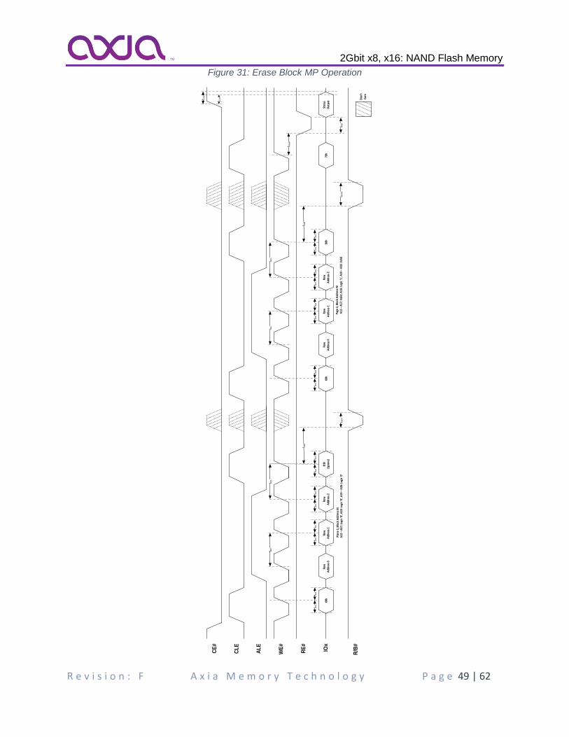
2Gbit x8, x16: NAND Flash Memory
R e v i s i o n : F A x i a M e m o r y T e c h n o l o g y P a g e 49 | 62
Figure 31: Erase Block MP Operation
CE
#
CL
E
AL
E
WE
#
RE
#
IOx
t DH
t DS
60h
t DB
SY
R/B
#
Row
Add
ress
0
t DH
t DS
Row
Add
ress
1
t DH
t DS
Row
Add
ress
2
t WC
t CH
Z
t CO
H
D1h
(Igno
re)
70h
Stat
usO
utpu
t
t DH
t DS
t AD
L
Don
tCa
re
t RE
A
t DH
t DS
60h
t BE
RS
Row
Add
ress
0
t DH
t DS
Row
Add
ress
1
t DH
t DS
Row
Add
ress
2
t WC
D0h
t DH
t DS
t AD
L
Plan
e 1,
Blo
ck A
ddre
ss M
Page
2, B
lock
Add
ress
M
A12
– A
17: L
ogic
A18
: Log
ic
A19
– A
28: L
ogic
A12
– A
17: V
alid
, A18
: Log
ic
A19
– A
28: V
alid
2Gbit x8, x16: NAND Flash Memory
R e v i s i o n : F A x i a M e m o r y T e c h n o l o g y P a g e 50 | 62
PROGRAM FOR DATA MOVE MP Operation
(85h – 11h - 81h – 10h) / (85h – 11h – 85h – 10h) The PROGRAM FOR DATA MOVE MP (85h-11h) command is functionally identical to the PROGRAM PAGE MP(85h-11h) command. Program for multi-plane data move program must be preceded by 2 single READ FOR DATA MOVE (00h-35h) (1st page must be read from the 1st plane and 2nd page from the 2nd
plane). Multi-plane copy back cannot cross plane boundaries: the contents of the source page of one plane can only be copied to a destination page in the same plane. Note that all commands are prohibited between 11h and 81h/80h except for READ STATUS REGISTER /
READ STATUS REGISTER MP/MD and RESET commands.
Note that the PROGRAM FOR DATA MOVE MP command is available only within two paired blocks in separate planes. This is accomplished in two ways:
1. (85h – 11h – 81h – 10h) - By setting the block address bits for the first plane to all zeros and the second address issued selects the block for both planes (plane address bit must be ‘1’ in the second address issued).
2. (85h – 11h – 85h – 10h) - Both addresses are issued in this protocol, however, the block address bits must be the same except for the bit(s) that select the planes.
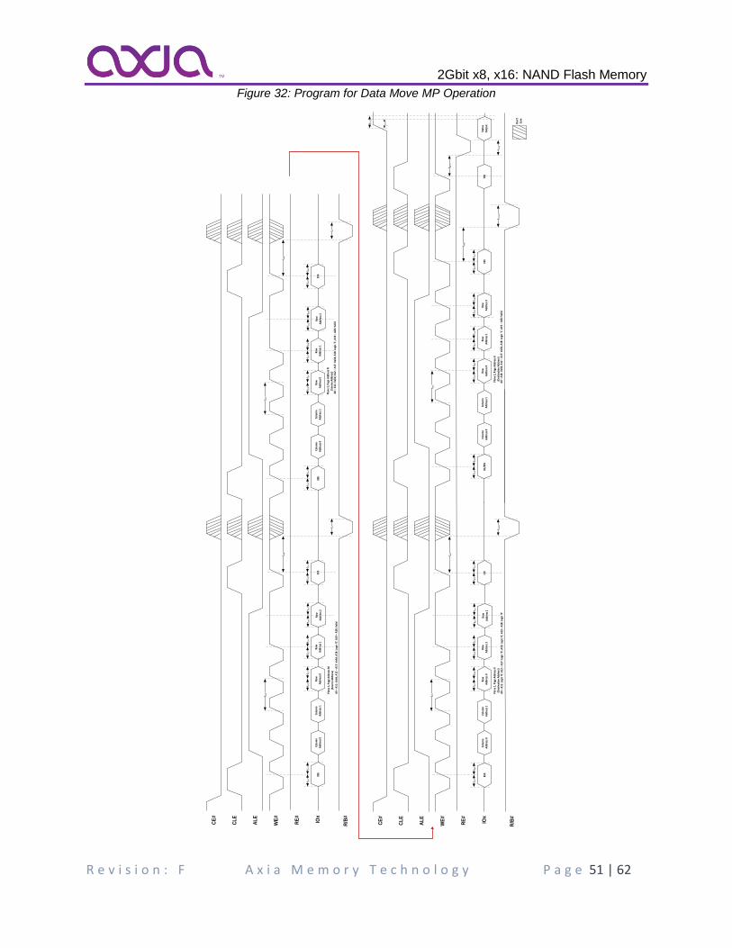
2Gbit x8, x16: NAND Flash Memory
R e v i s i o n : F A x i a M e m o r y T e c h n o l o g y P a g e 51 | 62
Figure 32: Program for Data Move MP Operation
CE
#
CL
E
AL
E
WE
#
RE
#
IOx
t DH
t DS
00h
Colu
mn
Add
ress
0
t R
R/B
#
Colu
mn
Add
ress
1
t DH
t DS
Row
Add
ress
0
t DH
t DS
Row
Add
ress
1
t DH
t DS
35h
t WC
t WB
t DH
t DS
Row
Add
ress
2
CE
#
CL
E
AL
E
WE
#
RE
#
IOx
t DH
t DS
85h
Colu
mn
Add
ress
0
t DB
SY
R/B
#
Colu
mn
Add
ress
1
t DH
t DS
Row
Add
ress
0
t DH
t DS
Row
Add
ress
1
t DH
t DS
11h
t WC
t WB
t DH
t DS
81/8
5hCo
lum
n A
ddre
ss 0
Row
A
ddre
ss 2
t PR
OG
Colu
mn
Add
ress
1
t DH
t DS
Row
Add
ress
0
t DH
t DS
Row
Add
ress
1
t WC
t CH
Z
t CO
H
10h
70h
Stat
usO
utpu
t
t DH
t DS
t DH
t DS
Don
tCa
re
t RE
A
t DH
t DS
Row
Add
ress
2
t DH
t DS
00h
Colu
mn
Add
ress
0
t R
Colu
mn
Add
ress
1
t DH
t DS
Row
Add
ress
0
t DH
t DS
Row
Add
ress
1
t DH
t DS
35h
t WC
t WB
t DH
t DS
Row
Add
ress
2
Plan
e 1,
Pag
e A
ddre
ss M
(S
ourc
e Ad
dres
s)
Plan
e 2,
Pag
e A
ddre
ss N
(S
ourc
e Ad
dres
s)
Plan
e 1,
Pag
e A
ddre
ss K
(D
estin
atio
n Ad
dres
s)Pl
ane
2, P
age
Add
ress
K
(Des
tinat
ion
Addr
ess)
A0
– A
11: L
ogic
A12
– A
17: L
ogic
A18
: Log
ic
A19
– A
28: L
ogic
A0
– A
11: V
alid
, A12
– A
17: V
alid
, A18
: Log
ic
A19
– A
28: V
alid
A0
– A
11: V
alid
, A12
– A
17: V
alid
, A18
: Log
ic
A19
– A
28: V
alid
A0
– A
11: V
alid
, A12
– A
17: V
alid
, A18
: Log
ic
A19
– A
28: V
alid
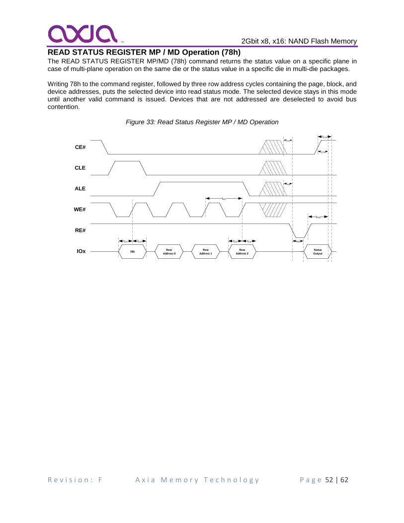
2Gbit x8, x16: NAND Flash Memory
R e v i s i o n : F A x i a M e m o r y T e c h n o l o g y P a g e 52 | 62
READ STATUS REGISTER MP / MD Operation (78h) The READ STATUS REGISTER MP/MD (78h) command returns the status value on a specific plane in case of multi-plane operation on the same die or the status value in a specific die in multi-die packages. Writing 78h to the command register, followed by three row address cycles containing the page, block, and device addresses, puts the selected device into read status mode. The selected device stays in this mode until another valid command is issued. Devices that are not addressed are deselected to avoid bus contention.
Figure 33: Read Status Register MP / MD Operation
CE#
CLE
ALE
WE#
RE#
IOx
tDHtDS
78hRow
Address 0StatusOutput
RowAddress 1
tDHtDS
RowAddress 2
tWC
tRHZ
tAR
tCLR
tCHZ
tCOH
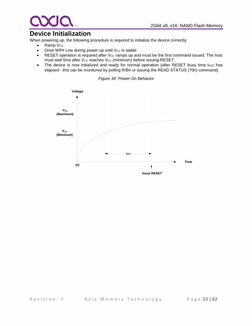
2Gbit x8, x16: NAND Flash Memory
R e v i s i o n : F A x i a M e m o r y T e c h n o l o g y P a g e 53 | 62
Device Initialization When powering up, the following procedure is required to initialize the device correctly:
• Ramp VCC.
• Drive WP# Low during power-up until VCC is stable
• RESET operation is required after VCC ramps up and must be the first command issued. The host must wait 5ms after VCC reaches VCC (minimum) before issuing RESET.
• The device is now initialized and ready for normal operation (after RESET busy time tRST has
elapsed - this can be monitored by polling R/B# or issuing the READ STATUS (70h) command).
Figure 34: Power-On Behavior
VCC
(Minimum)
VCC
(Maximum)
Voltage
Time
5ms
Issue RESET
0V
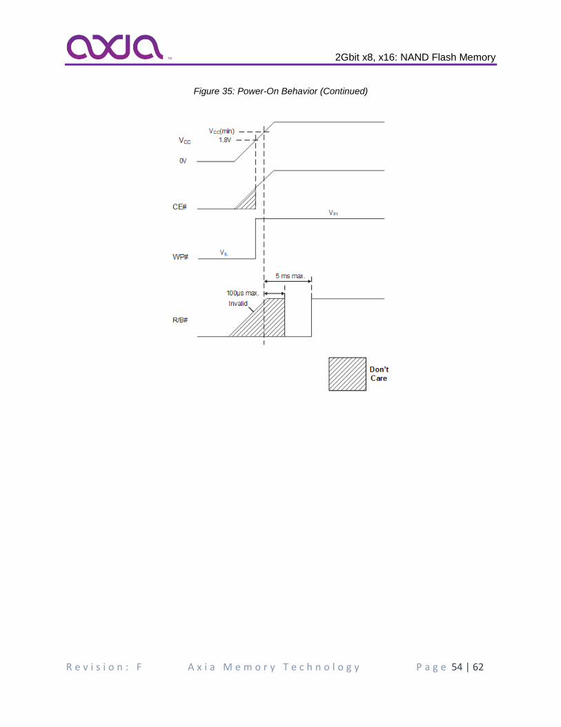
2Gbit x8, x16: NAND Flash Memory
R e v i s i o n : F A x i a M e m o r y T e c h n o l o g y P a g e 54 | 62
Figure 35: Power-On Behavior (Continued)
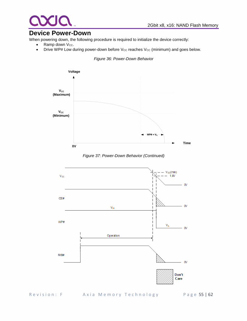
2Gbit x8, x16: NAND Flash Memory
R e v i s i o n : F A x i a M e m o r y T e c h n o l o g y P a g e 55 | 62
Device Power-Down When powering down, the following procedure is required to initialize the device correctly:
• Ramp down VCC.
• Drive WP# Low during power-down before VCC reaches VCC (minimum) and goes below.
Figure 36: Power-Down Behavior
VCC
(Minimum)
VCC
(Maximum)
Voltage
Time0V
Figure 37: Power-Down Behavior (Continued)
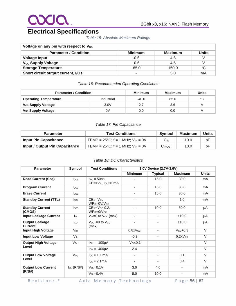
2Gbit x8, x16: NAND Flash Memory
R e v i s i o n : F A x i a M e m o r y T e c h n o l o g y P a g e 56 | 62
Electrical Specifications Table 15: Absolute Maximum Ratings
Voltage on any pin with respect to VSS
Parameter / Condition Minimum Maximum Units
Voltage Input -0.6 4.6 V
VCC Supply Voltage -0.6 4.6 V
Storage Temperature -65.0 150.0 °C
Short circuit output current, I/Os - 5.0 mA
Table 16: Recommended Operating Conditions
Parameter / Condition Minimum Maximum Units
Operating Temperature Industrial -40.0 85.0 °C
VCC Supply Voltage 3.0V 2.7 3.6 V
VSS Supply Voltage 0V 0.0 0.0 V
Table 17: Pin Capacitance
Parameter Test Conditions Symbol Maximum Units
Input Pin Capacitance TEMP = 25°C; f = 1 MHz; VIN = 0V CIN 10.0 pF
Input / Output Pin Capacitance TEMP = 25°C; f = 1 MHz; VIN = 0V CINOUT 10.0 pF
Table 18: DC Characteristics
Parameter Symbol Test Conditions 3.0V Device (2.7V-3.6V)
Minimum Typical Maximum Units
Read Current (Seq) ICC1 tRC = 50ns, CE#=VIL, IOUT=0mA
- 15.0 30.0 mA
Program Current ICC2 - 15.0 30.0 mA
Erase Current ICC3 - 15.0 30.0 mA
Standby Current (TTL) ICC4 CE#=VIH, WP#=0V/VCC
- - 1.0 mA
Standby Current (CMOS)
ICC5 CE#=VCC-0.2, WP#=0/VCC
- 10.0 50.0 µA
Input Leakage Current ILI VIN=0 to VCC (max) - - ±10.0 µA
Output Leakage Current
ILO VOUT=0 to VCC (max)
- - ±10.0 µA
Input High Voltage VIH 0.8xVCC - VCC+0.3 V
Input Low Voltage VIL -0.3 - 0.2xVCC V
Output High Voltage Level
VOH IOH = -100µA VCC-0.1 - - V
IOH = -400µA 2.4 - - V
Output Low Voltage Level
VOL IOL = 100mA - - 0.1 V
IOL = 2.1mA - - 0.4 V
Output Low Current (R/B#)
IOL (R/B#) VOL=0.1V 3.0 4.0 - mA
VOL=0.4V 8.0 10.0 - mA
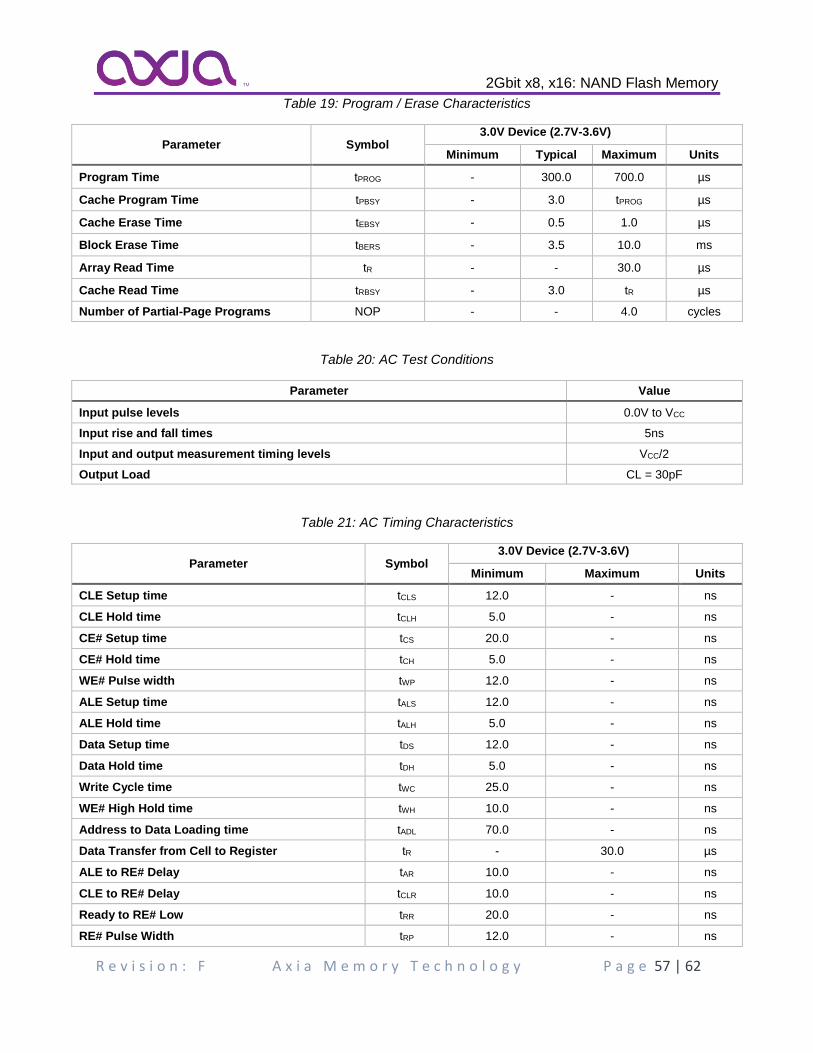
2Gbit x8, x16: NAND Flash Memory
R e v i s i o n : F A x i a M e m o r y T e c h n o l o g y P a g e 57 | 62
Table 19: Program / Erase Characteristics
Parameter Symbol 3.0V Device (2.7V-3.6V)
Minimum Typical Maximum Units
Program Time tPROG - 300.0 700.0 µs
Cache Program Time tPBSY - 3.0 tPROG µs
Cache Erase Time tEBSY - 0.5 1.0 µs
Block Erase Time tBERS - 3.5 10.0 ms
Array Read Time tR - - 30.0 µs
Cache Read Time tRBSY - 3.0 tR µs
Number of Partial-Page Programs NOP - - 4.0 cycles
Table 20: AC Test Conditions
Parameter Value
Input pulse levels 0.0V to VCC
Input rise and fall times 5ns
Input and output measurement timing levels VCC/2
Output Load CL = 30pF
Table 21: AC Timing Characteristics
Parameter Symbol 3.0V Device (2.7V-3.6V)
Minimum Maximum Units
CLE Setup time tCLS 12.0 - ns
CLE Hold time tCLH 5.0 - ns
CE# Setup time tCS 20.0 - ns
CE# Hold time tCH 5.0 - ns
WE# Pulse width tWP 12.0 - ns
ALE Setup time tALS 12.0 - ns
ALE Hold time tALH 5.0 - ns
Data Setup time tDS 12.0 - ns
Data Hold time tDH 5.0 - ns
Write Cycle time tWC 25.0 - ns
WE# High Hold time tWH 10.0 - ns
Address to Data Loading time tADL 70.0 - ns
Data Transfer from Cell to Register tR - 30.0 µs
ALE to RE# Delay tAR 10.0 - ns
CLE to RE# Delay tCLR 10.0 - ns
Ready to RE# Low tRR 20.0 - ns
RE# Pulse Width tRP 12.0 - ns
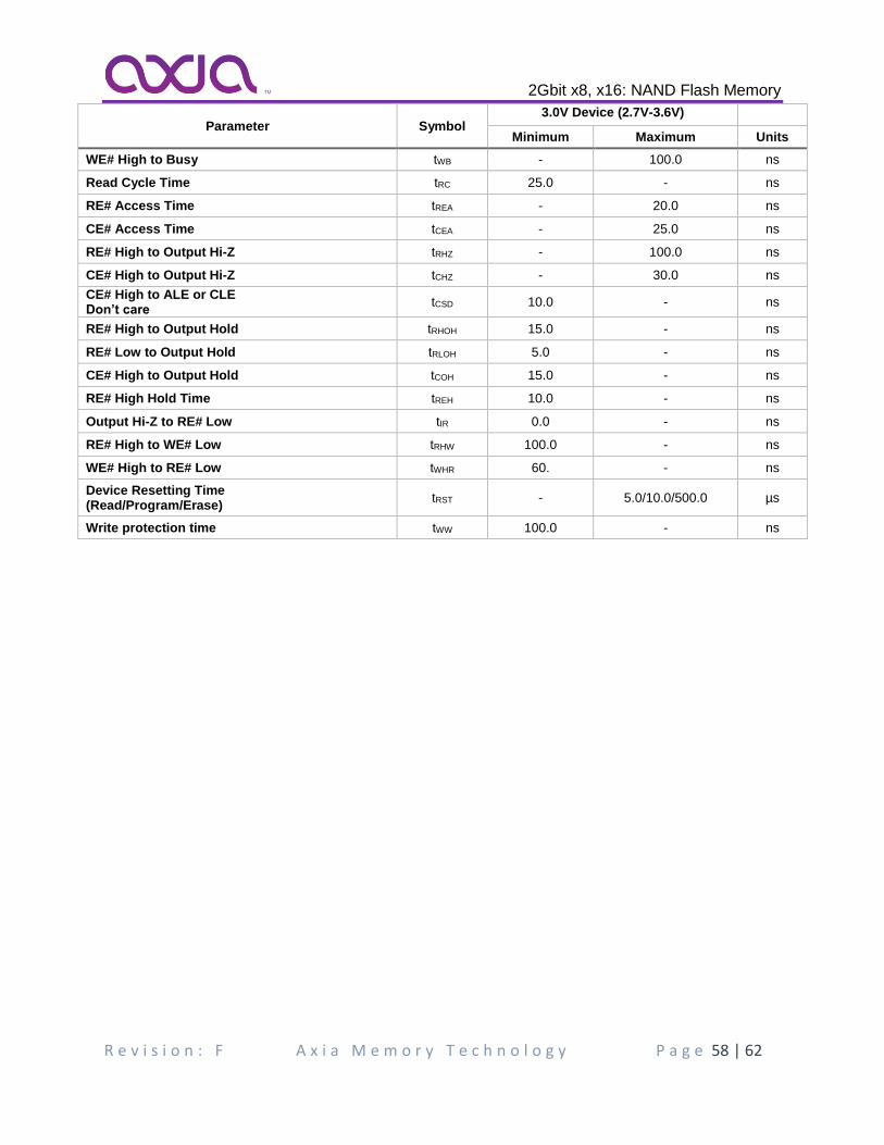
2Gbit x8, x16: NAND Flash Memory
R e v i s i o n : F A x i a M e m o r y T e c h n o l o g y P a g e 58 | 62
Parameter Symbol 3.0V Device (2.7V-3.6V)
Minimum Maximum Units
WE# High to Busy tWB - 100.0 ns
Read Cycle Time tRC 25.0 - ns
RE# Access Time tREA - 20.0 ns
CE# Access Time tCEA - 25.0 ns
RE# High to Output Hi-Z tRHZ - 100.0 ns
CE# High to Output Hi-Z tCHZ - 30.0 ns
CE# High to ALE or CLE Don’t care
tCSD 10.0 - ns
RE# High to Output Hold tRHOH 15.0 - ns
RE# Low to Output Hold tRLOH 5.0 - ns
CE# High to Output Hold tCOH 15.0 - ns
RE# High Hold Time tREH 10.0 - ns
Output Hi-Z to RE# Low tIR 0.0 - ns
RE# High to WE# Low tRHW 100.0 - ns
WE# High to RE# Low tWHR 60. - ns
Device Resetting Time (Read/Program/Erase)
tRST - 5.0/10.0/500.0 µs
Write protection time tWW 100.0 - ns
2Gbit x8, x16: NAND Flash Memory
R e v i s i o n : F A x i a M e m o r y T e c h n o l o g y P a g e 59 | 62
Error Management NAND Flash devices have bad blocks that are invalid when shipped from the factory. However, each NAND Flash device specifies a minimum number of valid blocks (NVB) of the total available blocks during the endurance life of the product. An invalid block is one that contains at least one page that has more bad bits than can be corrected by the minimum required ECC. Even though NAND Flash devices contain bad blocks, they can be used reliably in systems provided the systems have bad block management and error-correction algorithms. Axia’s NAND Flash devices are shipped from the factory erased. The factory identifies invalid blocks before shipping by providing a bad block marker (00h to FEh) into the 1st byte in the spare area of the 1st or 2nd page (if the 1st page is Bad). This method is compliant with ONFI Factory Defect Mapping requirements. System software should check the first spare area location on the first page of each block before performing any PROGRAM or ERASE operations on the NAND Flash device, thus creating a bad block table for the whole device. The following recommendations should be followed to achieve maximum reliability performance:
• Always check the program/erase status bits (PS1, PES2) after a PROGRAM or ERASE operation
• Use bad block management and wear-leveling algorithms
• The first block (physical block address 00h) is guaranteed to be valid with ECC when shipped from the factory (1K program/erase cycles)
Table 22: Error Management Details
Description Requirement
Minimum number of valid blocks (NVM) 2008
Total number of available blocks 2048
First spare area location x8: byte 2048, x16: word 1024
Bad block mark x8: 00h - FEh, x16: 0000h - FFFEh
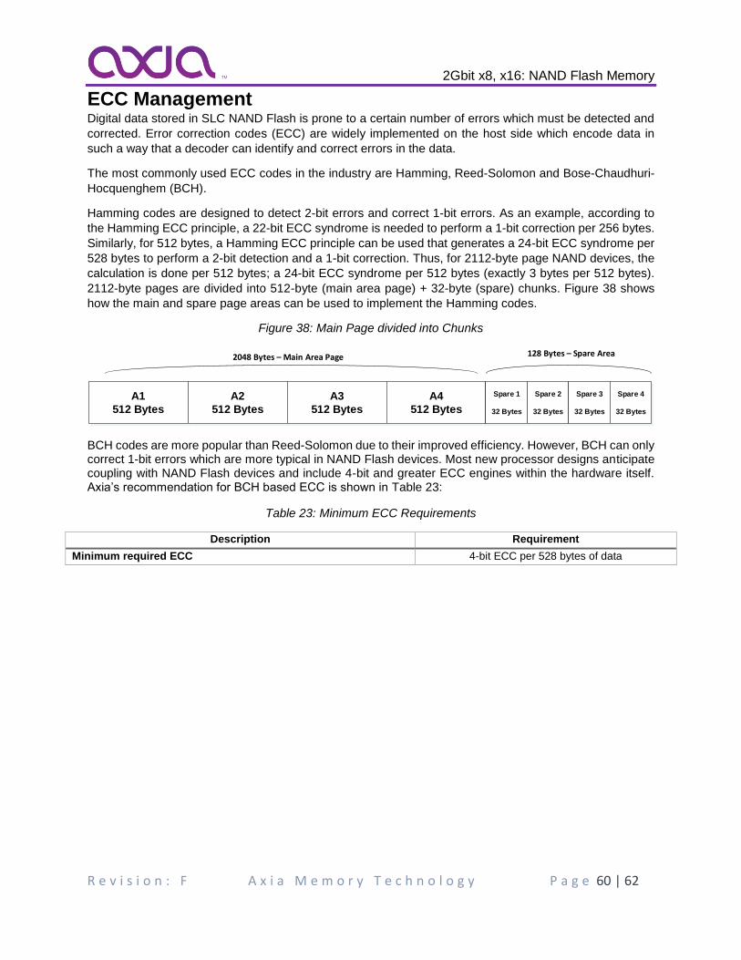
2Gbit x8, x16: NAND Flash Memory
R e v i s i o n : F A x i a M e m o r y T e c h n o l o g y P a g e 60 | 62
ECC Management Digital data stored in SLC NAND Flash is prone to a certain number of errors which must be detected and
corrected. Error correction codes (ECC) are widely implemented on the host side which encode data in
such a way that a decoder can identify and correct errors in the data.
The most commonly used ECC codes in the industry are Hamming, Reed-Solomon and Bose-Chaudhuri-
Hocquenghem (BCH).
Hamming codes are designed to detect 2-bit errors and correct 1-bit errors. As an example, according to
the Hamming ECC principle, a 22-bit ECC syndrome is needed to perform a 1-bit correction per 256 bytes.
Similarly, for 512 bytes, a Hamming ECC principle can be used that generates a 24-bit ECC syndrome per
528 bytes to perform a 2-bit detection and a 1-bit correction. Thus, for 2112-byte page NAND devices, the
calculation is done per 512 bytes; a 24-bit ECC syndrome per 512 bytes (exactly 3 bytes per 512 bytes).
2112-byte pages are divided into 512-byte (main area page) + 32-byte (spare) chunks. Figure 38 shows
how the main and spare page areas can be used to implement the Hamming codes.
Figure 38: Main Page divided into Chunks
A1
512 Bytes
A2
512 Bytes
A3
512 Bytes
A4
512 Bytes
Spare 1
32 Bytes
Spare 2
32 Bytes
2048 Bytes – Main Area Page 128 Bytes – Spare Area
Spare 3
32 Bytes
Spare 4
32 Bytes
BCH codes are more popular than Reed-Solomon due to their improved efficiency. However, BCH can only correct 1-bit errors which are more typical in NAND Flash devices. Most new processor designs anticipate coupling with NAND Flash devices and include 4-bit and greater ECC engines within the hardware itself. Axia’s recommendation for BCH based ECC is shown in Table 23:
Table 23: Minimum ECC Requirements
Description Requirement
Minimum required ECC 4-bit ECC per 528 bytes of data
2Gbit x8, x16: NAND Flash Memory
R e v i s i o n : F A x i a M e m o r y T e c h n o l o g y P a g e 61 | 62
Product Use Limitations Axia reserves the right to make changes to the information in this document, and related hardware, software
and system (collectively referred to as “Products”) without notice. This document supersedes and replaces
any and all prior or contemporaneous information or arrangement of any kind relating to the subject matter
hereof. This document and any information set forth herein may not be reproduced without the prior written
permission from Axia.
Critical Applications. Products are not authorized for use in applications in which failure of the Axia
component could result, directly or indirectly in death, personal injury, or severe property or environmental
damage ("Critical Applications"). Axia assumes no liability for Products if used for Critical Applications.
Should customer or distributor purchase, use, or sell any Axia component for Critical Applications, customer
and distributor shall indemnify and hold harmless Axia and its subsidiaries, subcontractors, and affiliates
and the directors, officers, and employees of each against all claims, costs, damages, and expenses and
reasonable attorneys' fees arising out of, directly or indirectly, any claim of product liability, personal injury,
or death arising in any way out of such Critical Application, whether or not Axia or its subsidiaries,
subcontractors, or affiliates were negligent in the design, manufacture, or warning of the Products.
Automotive Applications. Products are not authorized for use in automotive applications unless specified
by Axia. Axia assumes no liability for Products if used for automotive applications. Distributor and customer
shall assume the sole risk and liability for such use and shall indemnify and hold Axia harmless against all
claims, costs, damages, and expenses and reasonable attorneys' fees arising out of, directly or indirectly,
any claim of product liability, personal injury, death, or property damage resulting directly or indirectly from
any use of Products in automotive applications.
Military Applications. Products are not authorized for use in military applications, including without
limitation, for the design, development, use, stockpiling or manufacturing of nuclear, chemical, or biological
weapons or missile technology products (mass destruction weapons).
Customer Responsibility. Customers are solely responsible for the design and operation of their systems
using Products. It is customer’s sole responsibility to determine whether Products are suited for their
system. Customers are required to incorporate good safety design measures and adequate safeguards to
eliminate risks of personal injury, death, or severe property or environmental damages that could result
from failure of Products. AXIA ASSUMES NO LIABILITY FOR CUSTOMERS' PRODUCT DESIGN OR
APPLICATIONS AND DAMAGES OR LOSSES OCCURING AS A RESULT OF NONCOMPLIANCE
WITH APPLICABLE LAWS AND REGULATIONS.
The information contained herein is presented only as guidance for Product use. Axia assumes no
responsibility for any infringement of patents or any other intellectual property rights of third parties that
may result from the use of Products. No license to any intellectual property right is granted by this document,
whether expressed or implied. You may not perform compositional, structural, functional or other analysis
of Products, or undertake deconvolution or reverse engineering with respect to Products.
Limited Warranty
In no event shall Axia and its representatives be liable for any indirect, incidental, punitive, special or
consequential damages (including but not limited to loss of use, revenue or profit), whether or not such
damages are based on tort, warranty, breach of contract or other legal theory.
In no event shall Axia’s aggregate liability for any breach, warranty, indemnity or other obligation or liability
arising out of or in connection with the sale of Products or the use of any Products exceed the purchase
price of the particular Product(s) or services with respect to which losses or damages are claimed.
2Gbit x8, x16: NAND Flash Memory
R e v i s i o n : F A x i a M e m o r y T e c h n o l o g y P a g e 62 | 62
Revision History
Revision Date Change Summary
REV E 10/10/2018 Initial release
REV F 04/14/2019 Added Typ. to Endurance Updated Array Read Time (tR), Figure 35: Power-On Behavior (Continued), Figure 37: Power-Down Behavior (Continued)