multiwalled carbon nanotube films: fabrication …
TRANSCRIPT
MULTIWALLED CARBON NANOTUBE FILMS: FABRICATION TECHNIQUES AND APPLICATIONS
By
John Lucien Rigueur
Dissertation
Submitted to the Faculty of the
Graduate School of Vanderbilt University
in partial fulfillment of the requirements
for the degree of
DOCTOR OF PHILOSOPHY
In
Interdisciplinary Materials Science
May, 2012
Nashville, TN
Approved:
Professor Arnold Burger
Professor David Ernst
Professor Stephanie Getty
Professor Timothy Hanusa
Professor Charles Lukehart
Professor Norman Tolk

Copyright © 2012 by John Lucien Rigueur All Rights Reserved

ABSTRACT
The first part of the dissertation focuses on randomly oriented freestanding
films of multi-walled carbon nanotubes (MWCNTs), also known as buckypapers,
which have been fabricated by a two-step process using electrophoretic
deposition (EPD). These multi-walled carbon nanotubes films were cast onto
stainless steel electrodes from aqueous suspensions by EPD. Using a facile
mechanical cleavage technique, the films were liberated from their underlying
electrodes to yield the buckypapers. We investigated the films’ thickness,
morphology, and surface topology using, respectively, profilometry, scanning
electron microscopy, and atomic force microscopy. Mechanical characterization
of the buckypapers revealed the average tensile strength and Young’s modulus
to be 14.5 MPa and 3.3 GPa, respectively.
The second part of this dissertation focuses on vertically aligned multi-
walled carbon nanotubes. The purpose of our investigation was to optimize the
growth of catalyst assisted chemical vapor deposition (CVD) grown carbon
nanotubes for use as a photon absorbers in mid- to far-infrared applications.
Improvement of the height and density of the carbon nanotubes will effectively
increase the films absorptivity, bringing this material closer to an ideal absorber.
NASA is currently exploring the use of this technology towards improving the
stray light suppression of space flight instruments for future earth and space
science missions. Detrimental to these scientific instruments is the stray light
that scatters on interior telescope and instrument surfaces, thereby reducing the

performance of observational instruments. In order to control this undesired
effect, low-reflectance surface treatments are implemented in structural
instrument designs. Z306 black paint is traditionally used to absorb stray
photons, but advanced absorbers that employ films of multi-walled carbon
nanotubes have been shown to provide an order of magnitude improvement over
current surface treatments in the UV-visible-near infrared wavelengths. To this
end, we varied the thickness of the iron catalyst layer and deposition conditions;
varied hydrogen exposure times of substrates to optimize the MWCNT length
and film density for efficient absorption of longer wavelength photons. Scanning
electron microscopy is used to characterize film density and MWCNT height, and
hemispherical reflectance measurements are used to quantify performance of the
absorptive films.

iii
Dedicated
to
My grandmothers Pearl Christina Pacheco and Yvonne Cruishank, whom I lost
during this PhD. Journey, my mother Joan R Eastmond, and my aunt Janet
Eastmond, for their encouragement, support and belief in me to pursue my
graduate studies.

vi
AKNOWLEDGEMENTS
First and foremost I give thanks to GOD. Science to me is the pursuit of
conveying the message of GOD and with faith many aspirations are possible, we
must believe. I am an avid believer that we are given trials in life in order to
transcend beyond our innate being. From our experiences which may seem as
exams at times we arise anew like the mythological bird the phoenix. Where
some see chance or luck, I have come to view it as divine intervention unfolding
due to a faith the size of a mustard seed. Finding such a small seed within
ourselves requires devotion. For when faith intervenes, we must practice
humility and give thanks because every interaction we have is a greater piece to
the puzzle of our lives, our finite time here. And by these interactions we are
brought closer to a curious power within in us all. It is a marvelous wonder and
thus one can refer to this dissertation as “The Curious Case of John Lucien
Rigueur.”
For this reason I am grateful to the following individuals for aiding in my
dissertation. My advisor Professor Arnold Burger who has provided the
necessary support both professionally and personally allowing me to complete a
task not for me but for my Grandmother Pearl Pacheco whom I was fortunate to
visit in our home land of Trinidad and Tobago before she passed, I had never
experienced loss until this event. She birthed the curiosity in me, gave me an
unfounded confidence in my abilities, defined perseverance and has always told
her friends that I was going to the stars. Now something that I have worked on

vii
will be going to the stars. My NASA advisors Stephanie Getty PhD. and John
Hagopian, in September of 2010 my life took an unusual turn and it seems as
though chance or divine intervention favored me. I attended the NASA Graduate
Student Symposium arriving a day late to present my research conducted at
Vanderbilt University. I arrived with no intent on having meetings with anyone
one at NASA and met Mrs. Mablelene Burrell who emphasized that I get a
meeting with scientist at NASA. Following our conversation she got a meeting
with the educational office where I was informed of those doing exciting research
at NASA. It is in this meeting that I heard and wrote the name John Hagopian.
Following this meeting I was assigned to meet with Chuck Powers in the
Materials Directorate on my last day at the symposium. The outcome of this
meeting was a phone conference with Stephanie Getty from which my time at
NASA began in January 2011. I ask is this chance or divine intervention?
Stephanie I am truly indebted to you for your guidance, support and willing to
work with me to make me a more organized scientists. John H., I am also
indebted to you and I am thankful for your guidance and support, in addition to
securing additional support, though we still have to play that chess game.
I am also grateful to the members of my PhD committee Professors
Timothy Hanusa my committee chair who has been with me through graduate
school matriculation. Professor David Ernst, for your hard work and continual
words of encouragement and honesty; Professor Norman Tolk whose hard
questions and patience has pushed me to improve my scientific abilities; and
Professor Charles Lukehart whom was there in a great time of need, I thank you

viii
for being direct an honest with me I respond to this because it was how I was
raised. In addition I will like to thank NASA staff members Gregory Hidrobo,
Manuel Quijada, Chuck Powers, Michael Viens, Mark McClendon, Lynne Branch-
Foster, Lucy McFadden and Mablelene Burrell; the VINSE staff Anthony Melo,
Ben Schmidt, René Colehour and Sarah Satterwhite, the Fisk-Vanderbilt Bridge
staff Alyce Dobyns, Maggie Zilbut and Consti Coca.
In graduate school we have mentors, acquire new friends and research
associates which form our support group. I will like to thank my past group
members, Sameer Mahajan, Dustin Kavich, Sueseela Somarajan, Melissa
Harrison, Weidong Hei, Alex Krejci and Saad Hasan. Mentors are an important
part of life as such, Glenford Codrington, Walter Searcy III, Dr. Eugene W.
Collins, Dr. Lenard Feldman, Dr. Steve Morgan, Dr. Keivan Stassun, Dr. Princilla
Evans-Morris Dr. Bruce Vaughn and Dr. Don Brunson; you were all placed in my
life for a reason, thank you. My friends and support group, Jonathan Reynolds,
Bryan Kent Wallace, Tam’ra Kay Francis, Dawit Johwar, Anthony Price, Bruce
LeMont McMillan, Desmond Campbell, Thompson LeBlanc, Anh Hoang, Peter
Ciesielskie, Joy Garnett, Ebonee Walker, Charleson Bell, Shann Yu, Nichole
Renee Phillips, Hasting Hill and Jedidah Isler; for putting up with my highs and
lows.
Last but not least I would like to acknowledge Fisk University, my life was
changed forever considering I came without any financial support, only a dream
to be a mentor and example for my three younger brothers Jeffrey Rigueur,
Josue Rigueur and Jermain Rigueur and my son Jadon C Saunders-Rigueur.

ix
Finally my gratitude to my sister Giselle Anthony your discussions brought me
strength and reaffirmed my perseverance.
The research discussed in this dissertation was made possible with
financial support from the National Science Foundation Integrative Graduate
Education and Research Traineeship (IGERT) Fellowship for research in the
Nanosciences and from the NASA Harriet G. Jenkins Pre-doctoral Fellowship
Program.
I conclude with quotes from Albert Einstein which I live and treat the world
around me by:
"Problems are best solved at a different level of consciousness from which they are created.” "The intuitive mind is a sacred gift and the rational mind is a faithful servant. We have created a society that honors the servant and has forgotten the gift."

viii
TABLE OF CONTENTS
Page
DEDICATION ....................................................................................................... v
ACKNOWLEDGEMENTS ..................................................................................... vi
LIST OF TABLES ................................................................................................. x
LIST OF FIGURES ............................................................................................... xi
Chapter
1. INTRODUCTION .......................................................................................... 1
1.1. Structure of Nanotubes ............................................................................ 4
1.2. Electronic Structure of Nanotubes ........................................................... 7
1.3. Multi-Walled Carbon Nanotubes ............................................................. 11
1.4. Buckypapers ........................................................................................... 12
1.5. Synthesis Techniques of Nanotubes ...................................................... 12
1.6. Mechanism of CVD Growth and Growth Termination ............................ 13
1.7. Dissertation Organization....................................................................... 16
Works Cited ................................................................................................... 18
2. FABRICATION AND CHARACTERIZATION OF BUCKYPAPERS ............ 20
2.1. Introduction ............................................................................................ 20
2.2. Surfactant Characterization ................................................................... 22
2.3. Experimental .......................................................................................... 28
2.4. Discussion ............................................................................................. 31
2.5. Conclusion ............................................................................................. 49
Works Cited ................................................................................................... 50
3. OPTIMIZATION OF MULTI-WALLED CARBON NANOTUBE PHOTON
ABSORBERS FOR MID-AND FAR INFRARED STRAY LIGHT
SUPPRESSION IN SPACE INSTRUMENTATION ..................................... 52
3.1. Introduction ............................................................................................ 52
3.2. Methods ................................................................................................. 62
3.3. Growth of Vertically Aligned Multi-walled Carbon Nanotubes ................ 64
3.4. Raman Spectroscopy ............................................................................ 79
3.5. Optical Absorption and Reflection as Indicators of Performance ........... 83

ix
3.6. Conclusion .............................................................................................. 89
Works Cited ................................................................................................... 90
4. DETERMINATION OF OPTICAL PROPERTIES AND EFFECTS ON FILM
PERFORMANCE ....................................................................................... 92
4.1. Experimental Improvement of Reflectance ............................................. 92
4.2. Wavelength-Dependence Mechanisms of Reflection ............................. 97
4.3. Kramers-Kronig Relations ....................................................................... 98
Works Cited ................................................................................................. 104
5. CONCLUSIONS AND FUTURE WORK ................................................... 105
Appendix
A. ELECTROPHORETIC DEPOSITION THEORY ....................................... 107
B. PRELIMINARY EXPERIMENTS............................................................... 124

LIST OF TABLES
Table Page
1.1. Electronic properties of carbon-based materials ............................................ 2
2.1. Comparison of our BPs to other fabrication methods .................................. 45
2.2. Tensile strength and Young’s modulus comparison of BPs ......................... 46
3.1. H2 exposure times and growth results ......................................................... 69
3.2. Sample identifications (ID), iron (Fe) layer thickness, hydrogen exposure times, bulk mass, measured nanotube heights, calculated bulk densities and Average %R values ............................................................................................ 79 B.1. CVD runs (numbers) for samples with respective H2 exposure times…….124

xi
LIST OF FIGURES
Figure Page 1.1. Schematic diagram showing the different allotropes of carbon: the zero- dimensional (0D) carbon buckyballs, one-dimensional (1D) carbon nanotubes, two-dimensional (2D) graphene and three-dimensional (3D) diamond. ................ 2 1.2. Formation of single and multi-walled carbon nanotubes from graphene. The graphene sheet on the left is rolled to form a single walled nanotube (middle) and multi-walled carbon nanotube (right). ................................................................... 3 1.3. Chiral vector schematic defined on the honeycomb lattice of graphene, a1
and a2 are unit vectors, is the chiral angle with respect to the zigzag axis. ....... 5 1.4. Graphene sheet with unitary vectors specified by (n,m) integers for formation of nanotubes. Solid dots represent semiconducting tubes, encircled dots represent metallic tubes ....................................................................................... 6 1.5. (a)The unit cell of graphene in real space where carbon atoms are located at sites A and B. (b) The Brillouin zone in reciprocal space of graphene or 2D graphite layer, shaded hexagon and rhombus showing the high symmetry points
, K amd M. ai and bi (i = 1,2) are the basis and reciprocal lattice vectors respectively........................................................................................................... 9
1.6. (a)Tight binding electronic structure of graphene showing the , M and K
high symmetry points. (b) 3D model of (a) with the inclusion of the and * states, the K point is also displayed ...................................................................... 9 1.7. Reciprocal space of an armchair nanotube with the parallel lines along the tube axis (left) which results in metallic nanotubes. Reciprocal space of a zig zag nanotube with the parallel lines along tube axis (right) which results in semiconducting nanotubes. ................................................................................ 11 1.8. Schematic of root or extrusion growth and tip growth mechanisms ............. 14 1.9. Schematic demonstrating the effects of Ostwald ripening and subsurface diffusion of iron particles on an alumina surface ................................................. 16 2.1. TGA curves for as received un-centrifuged MWCNT and centrifuged MWCNT dispersions. Samples were drop-cast and allowed to dry in regular conditions (air) and heat dried at 120oC in a furnace .......................................... 24

xii
2.2. SEM image of un-centrifuged drop cast of MWCNT. Area shown in image was used for EDS analysis ................................................................................. 26 2.3. EDS spectra of un-centrifuged drop cast of MWNTs on stainless steel substrate. The C peak affirms the presence of MWNTs; the Na peak affirms the elemental composition of the proprietary surfactant and the O peak originates from the surfactant .............................................................................................. 26 2.4. EDS spectra of free-standing buckypaper. The C peak affirms the presence of MWNTs and the O peak originates from the surfactant .................................. 27 2.5. EPD scheme for the deposition of films of MWCNTs. The MWCNTs are surface functionalized with a negatively charged proprietary surfactant and deposited onto the positive electrode. The BK Precision power supply applies a voltage (2.8V) across the stainless steel electrodes. The Keithley records the current during EPD. Electrode spacing between electrodes was 1cm ................ 29 2.6. (a) TEM of MWCNT used in deposition, inner diameter of ~7 nm and outer diameter of ~25nm; scale bar 20 nm. SEM of MWCNT deposited onto stainless
steel substrates: (b) as received, scale bar 5 m and (c) centrifuged MWNTs,
scale bar 5 m. Inset of higher magnification SEM, scale bar 500 nm. .............. 32 2.7. Distribution of electrophoretic mobility for the centrifuged MWCNTs in an aqueous dispersion ............................................................................................ 34 2.8. Plots of (a) total mass and (b) thickness of MWCNTs films on stainless steel electrodes as functions of the number of depositions ......................................... 36 2.9. Current vs. time for the multi-deposition scheme. The initial spike in the current was due to the insertion of the electrodes into the solution of MWCNTs. The extraction of the electrodes occurred after 600 s. The additional film layers acted as resistive layers and as capacitive dielectric layers, which affected the measured current ............................................................................................... 37 2.10. (a) MWCNTs deposited on a stainless steel electrode prior to liberation; (b) image of the freestanding buckypaper fabricated from the mechanical cleavage technique. Film dimensions are 3.5 cm x 4.0 cm; (c) demonstration of films flexibility; and (d) demonstration of the film’s size scalability, which depends on the electrodes dimensions. (e) - (f)SEM images of a partially liberated MWCNT film from the stainless steel substrate showing complete film liberation; scale bar
(e) 300 m and (f) 500 m .................................................................................. 39 2.11. AFM images of (a) 1X and (b) 3X film deposited on stainless steel. RMS roughness of films is 14.4 and 14.5 nm, respectively ......................................... 40

xiii
2.12. Cross section SEM images, of 1X (a) and 3X (b) buckypapers with
thicknesses of 3.8 m and 6.9 m respectively: Scale bars are (a) 3 m and (b)
2.5 m. Graphs of (c) force - % strain, F is the change in force value and % is the change in strain value (d) stress - % strain of 1X and 3X buckypapers ........ 43 2.13. SEM images of samples subjected to load to failure testing, arrows indicate
direction of applied load. (a) 1X buckypaper; scale bar 2 m (b) unraveling (tube-tube shearing) of randomly oriented MWCNT network; scale bar 500 nm (c) 3X
buckypaper; scale bar 2 m and (d) 3X failure region similar to 9(b) for layer by layer deposition; scale bar 500 nm ..................................................................... 48 3.1. Calculated effective index of refraction and the absorption constant plotted as a function of nanotube spacing. A schematic of the nanotube array and the s and p light polarizations is displayed in the inset…………………………………..59 3.2. Sketch of (a) CVD furnace at zone 2 (center of furnace) and the location of samples with respect to the directional flow of gases (Ar, Ar/H2O, H2 and C2H4). The green colored sample is a reference (with only a 5 nm Fe layer) sample present in all growth runs (b) Growth steps of MWCNTs by the CVD method. .. 66 3.3. Thermal profile used for CVD growth of multi-walled carbon nanotubes where the variable is the H2 exposure time (flow rate of 580 sccm) relative to the introduction of C2H4 with a flow rate of 990 sccm. The carrier gas is dry Ar with a flow rate of 980 sccm (without H2O vapor) and wet Ar at 410 sccm (with H2O vapor). ................................................................................................................ 67 3.4. Mass of carbon for respective Fe catalyst layers for the t -15, t -10 and t -5 H2 exposure times. The masses of the t -15 and t -10 exposure times are relatively inconsistent. The t -5 H2 exposure time shows a linear trend for the mass as the catalyst layer increases. ................................................................. 71 3.5. SEM images of 23 nm (a) and 24 nm (b) samples displaying growth of nanotubes with the agglomeration of C atoms at the Al2O3 surface. The inset in (b) shows a higher magnification of this occurrence. The scale bars in the images are 200 nm. ........................................................................................................ 72 3.6. Heights of nanotubes (averaged) as measured by SEM for t -5, t -10 and t -15 H2 exposure times. t -5 heights are approximately the same within error, t -10 heights have a linear trend and t -15 show no trend. .......................................... 73
3.7. Average bulk density ( B) of nanotubes as a function of the catalyst thicknesses for t -5, t -10 and t -15 H2 exposure times. The bulk density of the t -5 exposure time is relatively linear with an R2 value of 0.98. ................................. 75 3.8. Relationship between reflectance (%R) and (a) bulk density and (b) areal density for our samples. ..................................................................................... 76

xiv
3.9. SEM image of contaminated 4nm sample. The striations shown in the inset caused regions of non-uniform growth, resulting in higher %R values. .............. 76 3.10. Raman shift spectra for t -5 H2 exposure time. The radial breathing mode (RBM) is present for some of our samples and is located in the range of 230 – 235 cm-1and is typically used to calculate the diameter of single-walled CNTs. In addition we observe the presence of the D, G and G’ –band peaks with intensities in the range of ~1318-1321 cm-1, 1577-1585 cm-1 and 2600 cm-1 ,
respectively. Laser beam diameter and power were 2 m and 13 mW respectively......................................................................................................... 81 3.11. The G dispersion (Gd) and ID/IG ratio for the t -5 H2 exposure time. The 2 nm sample exhibits lower impurity defects. ........................................................ 82 3.12. SEM images showing the helical nature of our nanotubes. ....................... 82 3.13. (a) Shows the peak located at 275 nm (4.5 eV) in the ultraviolet spectrum (UV). (b) Measured hemispherical reflectance of t -5 exposure time (lowest averaged reflectance showed these as our best samples) for the near infrared (IR) spectrum. ..................................................................................................... 87 3.14. (a) Shows the peak located at 275 nm (4.5 eV) in the ultraviolet spectrum (UV). (b) Measured hemispherical reflectance of t -10 exposure time (best performing samples) for the near infrared (IR) spectrum. The 24 nm sample
shows the onset of -dependence. .................................................................... 88 3.15. Measured hemispherical reflectance of t -15 exposure time (best performing samples) for the near infrared (IR) spectrum. Inset shows the peak located at 275 nm (4.5 eV) in the ultraviolet spectrum (UV). .............................. 88 4.1. Measured hemispherical reflectance of (a) t =0 and (b) t -5 exposure times before and after O2 plasma etch for an 8 nm Fe catalyst layer growth on silicon. The UV-VIS-NIR spectrum is plotted. The UV peaks are located at 275 nm (4.5 eV), though there is a shift to higher wavelength (lower energy/frequency) for t =0. The reflectance increases linearly after plasma etching for the t -5 sample, an approximate five-fold increase. ...................................................................... 93
4.2. SEM image of CNTs with a height of ~ 35 m. Region I is the surface of the aligned nanotubes which exhibit bridge-like interconnections. Region II shows highly aligned nanotubes with helical growth and Region III is the base where growth begins. .................................................................................................... 94 4.3. SEM images of (a) t =0 before O2 plasma etch (b) t -5 before O2 plasma etch (c) t =0 after O2 plasma etch and (d) t -5 after O2 plasma etch. Insets in (a) and

xv
(b) are higher magnifications of film. Scale bars are 200 nm, for regular and insets. ................................................................................................................. 96 4.4. Measured hemispherical reflectance for (a) t =0 Si 8 nm catalyst thickness at 0o and 8o angles of incidence (b) t -5 Si 8 nm catalyst thickness at 0o and 8o angles of incidence. In (b) we observe the absence of the specular component, suggesting that the linear wavelength-dependence is a component of specular reflection. ............................................................................................................ 98 4.5. Smoothed reflectance data for a t -5 Si 8 nm catalyst thickness and the extrapolations used (a) before plasma etch and (b) after plasma etch. ............ 102 4.6. Phase data for a t -5 Si 8 nm catalyst thickness (a) before plasma etch and (b) after plasma etch. ........................................................................................ 102
4.7. Calculated ( ), with real and imaginary components for t -5 Si 8 nm
catalyst thickness. (a)Re ( ) before plasma etch (b) Re ( ) after plasma etch
(c) Im ( ) before plasma etch (d) Re ( ) after plasma etch. ........................ 103

1
CHAPTER 1
INTRODUCTION
Carbon, one of the most abundant elements found on earth has unique
properties due to its spn – hybridized bonds which lead to the many carbon
allotropes, ranging from zero to three dimensions on the nanoscale. These
allotropes of carbon (Figure 1.1), the zero- dimensional (0D) carbon buckyballs,
one-dimensional (1D) carbon nanotubes, two-dimensional (2D) graphene and
three-dimensional (3D) diamond, make it a highly investigated material for a wide
range of nanotechnology applications [1]. On the nanoscale, materials behave
differently from their bulk counterparts, due to the effects of quantum
confinement; Table 1 shows the effects dimensionality has on the unique
properties of the allotropes of carbon. From the perspective of materials science,
these materials possess intriguing chemical, physical and electronic properties
that have attracted the global community of scientists to investigate applications
in advanced technological devices. Of the allotropes of carbon, carbon
nanotubes (CNTs) have led the charge since their discovery in 1991 by Iijima [2].

2
Figure 1.1.[1] Schematic diagram showing the different allotropes of carbon: the zero- dimensional (0D) carbon buckyballs, one-dimensional (1D) carbon nanotubes, two-dimensional (2D) graphene and three-dimensional (3D) diamond.
Table 1.1. Electronic properties of carbon-based materials [1]
Electron Mobility (cm
2 V
-1s
-1)
Bandgap (eV) Thermal Conductivity (W cm
-1 K
-1)
Diamond 2200 5.45 22
Carbon Nanotubes 1 x 10⁵ (0 to 1) 30
Graphene 1 x 10⁴ to 2 x 10
5 (0 to 0.5) 40

3
Carbon nanotubes (CNTs) were discovered using the arc discharge
production method. CNTs can be described as single or multiple sheets of
graphene with a hexagonal ring structure, rolled into a cylindrical shape as
shown in Figure 1.2. As produced, they are usually linear, exhibiting long-range
order parallel to the axis of the nanotube. Nanotubes are composed of sp2
bonded carbon, which is a factor for its unique mechanical, thermal, electronic
and optical properties. There are several types of carbon nanotubes (CNTs)
widespread in the scientific research; single-walled (SW), doubled-walled (DW)
and multi-walled (MW), as shown in Figure 1.2 respectively.
Figure 1.2.[3] Formation of single and multi-walled carbon nanotubes from
graphene. The graphene sheet on the left is rolled to form a single walled nanotube (middle) and multi-walled carbon nanotube (right).

4
1.1. Structure of Nanotubes
Carbon nanotubes, due to their small diameter (~10 Å) and large length to
diameter (aspect ratio) (>103), provide an important system for studying one-
dimensional physics, theoretically and experimentally [4]. To understand the
structure of CNTs, we investigate a sheet of 2D graphene rolled to form a 1D
SWCNT and identify mathematically the alternate forms of chirality since the
traditional view of a tube is a rolled up sheet of graphene. The chiral vector hC ,
which spans the circumference of a CNT, is used to identify how a graphene
sheet can be rolled up into cylindrical form. The chiral vector hC is defined as;
21 amanCh
1.1
where a1 and a2 are the unit vectors of graphite and n and m are arbitrary
integers. As depicted in Figure 1.3, a (n, m) nanotube is formed by rolling the
graphene sheet into a cylinder in order for atoms O and A, or B and B’ to be
connected by the chiral vector. The diameter of a single tube (tubule) can be
expressed as;
2/12 )(3 nmnmaCd
CCh
t 1.2
where aC-C is the nearest neighbor distance (1.42Å in graphite), hC is the length
of the chiral vector and the chiral angle equation is given by,
nm
m
2
3tan 1 [4] 1.3

5
Figure 1.3.[4] Chiral vector schematic defined on the honeycomb lattice of
graphene, a1 and a2 are unit vectors, is the chiral angle with respect to the zigzag axis.
The chiral vector determines the rolling direction of the graphene sheet
where each carbon atom is located at the vertex of the hexagon lattice structure
for which lattice point integers (n, m) are superimposed with an origin defined as
(0, 0), resulting in chiral nanotubes[2, 4]. As a result of the chiral vector, where
each integer pair (n, m) defines a singular approach of rolling the graphene sheet
we form three rolling orientations (chiral, zigzag and armchair); see Figure 1.4 of
a carbon nanotube[5]. The chiral angle and lattice vector representations of the

6
nanotube in the zigzag direction is = 0, where it has lattice vector values of (n,
0) and of the armchair = 30o, while its lattice vector values are (n, n). Both the
(n, 0) and (n, n) nanotubes have especially high symmetry and exhibit a mirror
symmetry plane normal to the tubule axis.
The lattice constant and intertube spacing are a necessity to generate
SWCNTs and MWCNTs, where these parameters vary in tube diameter or radial
direction. Most experimental measurements and theoretical calculations agree
that the C-C bond length 42.1CCd and 46.221 aaa and intertube
spacing 4.3ttd[6]. Since both right and left-handed chirality is possible for
chiral tubules, it is expected that chiral tubules are optically active to either right
or left circularly polarized light propagating along the tubule axis.
Figure 1.4.[4] Graphene sheet with unitary vectors specified by (n,m) integers for formation of nanotubes. Solid dots represent semiconducting tubes, encircled dots represent metallic tubes.

7
The fundamental translation vector given by ),( mn
is located along the
tube axis and is perpendicular to hC
. The length of the Brillouin zone isT
2,
where a for an armchair nanotube and a3 for zigzag nanotubes. In
general, for any (n,m) nanotube,
R
t
R d
dC
d
33 1.4
where Rd is the greatest common divisor of (2n+m) and (2m+n).
1.2. Electronic Structure of Nanotubes
The bonding of carbon nanotubes consists of sp2 (spXpY) hybridized bonds
which is similar to that in graphene. Figure 1.5.a shows the unit cell and basis
vectors for graphene in real space, where these bonds are planar in
characteristic and occur when the 2s and 2pXY-shells of each carbon atom are
combined with the 2s- and 2pXY-shells of its neighboring atoms, forming bonds
that have both s and p character. The bonds formed are the strong covalent or
bonds and the weak bond based on interaction of the pZ orbital, allowing each
carbon atom to have three bonds and one bond. These sp2 bonding
characteristics may be used to approximate the bonds in cylindrical carbon
nanotubes. Since perfect nanotubes encompass a uniform diameter,
observation has shown defects in bonding that allow sp3 bonding to occur. This
bonding mechanism may produce defects, such as pentagons and heptagons, in
the perfect hexagonal structure. Through the gradual narrowing and widening of

8
nanotubes these defects may be observed[7]. The tubular structure of a
nanotube then can be described with a sp2 – sp3 bonding characteristic, to
account for the defects.
In order to understand the electronic properties a zone folding tight binding
method is used to map the band structure of graphene to construct the Brillouin
zone (BZ) of a SWCNT. This method takes into account only confinement
effects and neglects the contribution of curvature[8]. Figure 1.5.b shows the
hexagonal BZ of graphene, in reciprocal space whose sides are CCa3/1 from the
center. The BZ contains one electron per atom thus graphite is zero-gap
semiconductor or semimetal ( - * overlapping). The Fermi surface is reduced to
six points at the hexagonal BZ corners where the 2D graphene electronic
structure near the Fermi energy is given by occupied (valence) band and an
empty * (conduction) band. These bands have a linear dispersion in )(kE near
the K point.
Based on Wallace’s model [9] the energy dispersion )(kE of the and *
bands are calculated based on the nearest-neighbor tight binding model. Thus
2/1
02
2cos42
cos2
3cos41),(
akakakkkE YYX
YX 1.5
where 0 is the overlap integral between nearest-neighbor carbon atoms and the
± refer to the * and bands, respectively. Figure 1.6.a and b shows the 2D and
3D energy bands for graphene based on calculations from equation 1.5. We
observed at the K points the vanishing of the energy gap where the Fermi
energy, EF, is 0FE ; consequently these K points are important for electric

9
Figure 1.5.[8] (a)The unit cell of graphene in real space where carbon atoms are located at sites A and B. (b) The Brillouin zone in reciprocal space of graphene or 2D graphite layer, shaded hexagon and rhombus showing the high symmetry
points , K amd M. ai and bi (i = 1,2) are the basis and reciprocal lattice vectors respectively.
Figure 1.6.[8] (a)Tight binding electronic structure of graphene showing the , M
and K high symmetry points. (b) 3D model of (a) with the inclusion of the and * states, the K point is also displayed.
a b
a b

10
transport. Two consequences arise when deriving a nanotube from graphene;
i. The size of the first BZ in the tubule axis direction is determined by the
translational period t, where tk II /2 and the wave vector is continuous.
ii. The wave vector is quantized in the direction related to the
circumference (k┴) due to the periodic boundary conditions;
mChk 2 1.6
md
mC
kt
22 1.7
where m is an integer. Therefore in terms of the 2D BZ of graphene, the allowed
k states for nanotubes lie along parallel lines separated by a distance given by
equation 1.7 which has a dependence on diameter and chirality. Figure 1.7
shows the allowed k states for armchair (n,n) tubes, where these quantized wave
vectors lie on K points. This results in metallic behavior for nanotubes with this
outcome. For zig zag (n,0) chiral tubes, the quantized wave vectors lie off
centered to the Fermi points allowing energy gaps which give zig zag nanotubes
semiconducting or metallic behavior.

11
Figure 1.7.[10] Reciprocal space of an armchair nanotube with the parallel lines along the tube axis (a) which results in metallic nanotubes. Reciprocal space of a zig zag nanotube with the parallel lines along tube axis (b and c) which results in semiconducting nanotubes.
1.3. Multi-Walled Carbon Nanotubes
MWCNTs consist of multiple concentric layers of graphite, with the
identical interlayer distance of ~0.34 Å. They were discovered first by Iijima [2] in
1991 via the arc discharge method. As grown by the CVD method, MWCNTs are
perpendicular to the substrate surface. Mizuno et al. [11] demonstrated that the
absorptive properties (blackbody behavior) are dependent on the vertical
alignment (forest-like structures) normal to substrate.

12
1.4. Buckypapers
Buckypapers (BPs) are a macroscopic or ensemble form of
nanotubes formed into films (composed of SW, DW or MW) that are randomly
oriented onto the substrate. Since BPs are formed from the random orientation
of nanotubes, the electrical and mechanical properties are a bulk composite
effect of the numerous nanotube interactions; such as nanotube-nanotube
junctions. The BP orientation plays a role into the macro-properties and hence
applications. For instance, when randomly oriented in porous networks parallel
to the substrate, it can be used as a composite material, in filtration, for thermal
dispersion and electrostatic coatings [12-18]. When grown into “forest” structures, it
can be utilized for field emission and photon absorption. Wang et al. [19] showed
that highly oriented tubes parallel to the substrate can increase the Young’s
modulus and tensile strength.
1.5. Synthesis Techniques of Nanotubes
Conventionally, CNTs are synthesized by several techniques: (1) chemical
vapor deposition (CVD), a gas phase thermal decomposition process; (2) arc
discharge, a high current electric arc that goes through high purity graphite
electrodes in the presence of catalytic particles in a He atmosphere to form
carbon nanotubes and soot on the cathode; and (3) laser ablation, which uses a
Nd-YAG high power laser for the vaporization of pure graphite targets or graphite
powders in an Ar atmosphere and a furnace temperature of 1200 oC. Though all

13
these techniques produce nanotubes, CVD has emerged as the most practical
process for the fabrication of CNTs due to the ability to tune experimental
parameters. The advantages of the CVD method are the following;
Provides a means of growing on the bulk scale as well as on substrate
surface
A more versatile technique; SWCNT, DWCNT, and MWCNT can be
synthesized by tuning the parameters [20-22] (carbon feedstock gas,
temperature, catalyst, etc.)
Cost effective.
1.6. Mechanism of CVD Growth and Growth Termination
The CVD method uses several metal catalysts, such as iron (Fe), cobalt
(Co), and nickel (Ni) in addition to carbon-containing compounds such as
methane and ethylene. Both SW- and MWCNTs can be grown via this method
dependent on catalyst parameters and feedstock gas. The initial stage typically
consists of depositing the catalyst layer onto a substrate. The substrate and
catalyst are then heated to a designated temperature. During this heating, the
catalyst layer forms “clusters” which vary in size. This size variation accounts for
the size distribution observed in nanotubes grown. At the specified temperature
(in our case 750 oC), the catalyst forms a liquid nanoparticle “island”
supersaturated with hydrocarbon molecules. The size of the “island” depends on
the substrate roughness and reaction parameters (gas flow rate, temperature
gradient, etc.) [23-27].

14
Figure 1.8. [25] Schematic of root or extrusion growth and tip growth mechanisms.
Figure 1.8 is a schematic of the growth models, root and tip, for the CVD
method. As depicted in the root growth model, the catalyst particle has a critical
radius of curvature, resulting from the extremely small diameter of the catalyst
particle, allowing the formation of graphite crystallites with a basal plane
formation oriented tangential to the curved surface [23]. The large strain on the
basal plane forces them to form the crystalline nanotube structure. In the tip
growth model, the formation of the catalyst particle and nucleation of carbon
atoms occur as explained above. However in this mechanism, the weak catalyst
particle-crystalline nanotube interaction causes the particle to lift-off with the
continual growth of the nanotube structures. Growth ceases when the particle
surface is covered with carbon and/or when the feedstock is terminated [23].
In Chapter 3, our substrate preparation consisted of depositing the
catalyst onto an alumina (Al2O3) layer to improve adhesion to the substrate [28].

15
Kim et al. [27] showed that Ostwald ripening and subsurface diffusion led to the
loss of catalytic activity which leads to growth termination, as depicted in Figure
1.9. Ostwald ripening is a thermodynamically spontaneous process where larger
particles are more energetically favored than smaller particles as a result of
surface molecules being less energetically stable than the interior particles. The
expression for Ostwald ripening is
tTR
DcRR
go 9
8 233
1.4
where R is the average radius of all the particles, is the particle surface
tension or surface energy, c∞ is the solubility of the particle material, the molar
volume of the particle material, D the diffusion coefficient of particle material, Rg
is the ideal gas constant and T the absolute temperature. The particle size
distribution was described by Ostwald ripening up to 5 minutes of thermal
annealing; beyond this point the total number density of particles decreased
giving rise to subsurface diffusion of the catalyst into the Al2O3 layer. This metal
cluster formation within the alumina layer is a result of the surface metal atom’s
mobility in addition to the long term stability of clusters of metal atoms with bulk-
like coordination in the alumina pores [27, 29].

16
Figure 1.9. [27] Schematic demonstrating the effects of Ostwald ripening and subsurface diffusion of iron particles on an alumina surface.
1.7. Dissertation Organization
This dissertation is organized as follows. Chapter 1 gives an introductory
review of the underlying material, carbon, and looks at the 1D allotrope for
research purposes. Chapter 2 focuses on the electrophoretic deposition (EPD)
of aqueous suspensions of MWCNTs which are deposited onto stainless steel
substrates. Further we demonstrate the development of a new and unique
procedure to attain free-standing BPs. Chapter 3 focuses on the previous work
utilizing vertically aligned MWCNTs as photon absorbers and concentrates on
the optimization of CVD grown vertically aligned MWCNTs for direct technology
applications for photon absorption in NASA’s space and earth-based telescopes.
Chapter 4 focuses on methods to improve the absorptive abilities of our films and
analysis of our reflectance data using the Kramers-Kronig analysis. Chapter 5

17
summarizes the content of this dissertation and discusses possible future
directions of this work.

18
Works Cited
1. Guisinger, N.P. and M.S. Arnold, Beyond Silicon: Carbon-Based Nanotechnology. MRS Bulletin, 2010. 35(4): p. 273-279.
2. Iijima, S., Helical microtubules of graphitic carbon. Nature, 1991. 354(6348): p. 56-58. 3. Graham, A., et al., How do carbon nanotubes fit into the semiconductor roadmap?
Applied Physics A: Materials Science & Processing, 2005. 80(6): p. 1141-1151. 4. Dreselhaus, M.S., G. Dresselhaus, and P.C. Eklund, Science of Fullerenes and Carbon
Nanotubes. 1996. 5. Terrones, M., Science and technology of the twenty-first century: synthesis, properties,
and applications of carbon nanotubes. Annual Review of Materials Research, 2003. 33(1): p. 419-501.
6. Meyyappan, M., Carbon nanotubes: science and applications. 2005: CRC. 7. Kiang, C.H., et al., Size effects in carbon nanotubes. Physical Review Letters, 1998. 81(9):
p. 1869-1872. 8. Dresselhaus, M., G. Dresselhaus, and A. Jorio, Unusual properties and structure of
carbon nanotubes. Annu. Rev. Mater. Res., 2004. 34: p. 247-278. 9. Wallace, P., The band theory of graphite. Physical Review, 1947. 71(9): p. 622. 10. Dai, H., Carbon nanotubes: opportunities and challenges. Surface Science, 2002. 500(1-
3): p. 218-241. 11. Mizuno, K., et al., A black body absorber from vertically aligned single-walled carbon
nanotubes. Proceedings of the National Academy of Sciences, 2009. 106(15): p. 6044. 12. Ci, L., et al., Ultrathick freestanding aligned carbon nanotube films. Advanced Materials,
2007. 19(20): p. 3300-3303. 13. Ruoff, R.S. and D.C. Lorents, Mechanical and thermal properties of carbon nanotubes.
Carbon, 1995. 33(7): p. 925-930. 14. Datsyuk, V., et al., Chemical oxidation of multiwalled carbon nanotubes. Carbon, 2008.
46(6): p. 833-840. 15. Jason, J.G., et al., Assembly of well-aligned multiwalled carbon nanotubes in confined
polyacrylonitrile environments: electrospun composite nanofiber sheets. Journal of the American Chemical Society, 2004. 126(48): p. 15754-15761.
16. Ago, H., et al., Composites of carbon nanotubes and conjugated polymers for photovoltaic devices. Advanced Materials, 1999. 11(15): p. 1281-1285.
17. Safadi, B., R. Andrews, and E. Grulke, Multiwalled carbon nanotube polymer composites: synthesis and characterization of thin films. Journal of Applied Polymer Science, 2002. 84(14): p. 2660-2669.
18. Moisala, A., et al., Thermal and electrical conductivity of single-and multi-walled carbon nanotube-epoxy composites. Composites Science and Technology, 2006. 66(10): p. 1285-1288.
19. Wang, D., et al., Highly oriented carbon nanotube papers made of aligned carbon nanotubes. Nanotechnology, 2008. 19: p. 075609.
20. Nessim, G.D., et al., Tuning of vertically-aligned carbon nanotube diameter and areal density through catalyst pre-treatment. Nano Letters, 2008. 8(11): p. 3587-3593.
21. Grujicic, M., G. Cao, and B. Gersten, Optimization of the chemical vapor deposition process for carbon nanotubes fabrication. Applied surface science, 2002. 191(1-4): p. 223-239.
22. Nessim, G.D., et al., Precursor gas chemistry determines the crystallinity of carbon nanotubes synthesized at low temperature. Carbon, 2010. 49(3): p. 804-810.

19
23. Kunadian, I., et al., Growth kinetics of MWCNTs synthesized by a continuous-feed CVD method. Carbon, 2009. 47(2): p. 384-395.
24. Yun, Y.H., et al., Growth mechanism of long aligned multiwall carbon nanotube arrays by water-assisted chemical vapor deposition. The Journal of Physical Chemistry B, 2006. 110(47): p. 23920-23925.
25. Sinnott, S., et al., Model of carbon nanotube growth through chemical vapor deposition. Chemical Physics Letters, 1999. 315(1-2): p. 25-30.
26. Nessim, G.D., et al., The critical role of the underlayer material and thickness in growing vertically aligned carbon nanotubes and nanofibers on metallic substrates by chemical vapor deposition. Advanced Functional Materials, 2010. 20(8): p. 1306-1312.
27. Kim, S.M., et al., Evolution in catalyst morphology leads to carbon nanotube growth termination. The Journal of Physical Chemistry Letters, 2010. 1(6): p. 918-922.
28. Hagopian, J.G., et al. Multiwalled carbon nanotubes for stray light suppression in space flight instruments. in Proceedings of SPIE. 2010: SPIE.
29. Colaianni, M., P. Chen, and J. Yates Jr, Spectroscopic studies of the thermal modification of the Fe/Al2O3 interface. Surface science, 1990. 238(1-3): p. 13-24.

20
CHAPTER 2
FABRICATION AND CHARACTERIZATION OF BUCKYPAPERS
2.1. Introduction
Since the discovery of carbon nanotubes (CNTs), growth in scientific
interest associated with the fabrication of CNT assemblies has been motivated
by the desire to incorporate CNTs into devices that exploit their attractive
electrical, mechanical, and thermal properties. Macroscopic CNT assemblies,
such as yarns, films, and arrays, can be fabricated by an assortment of methods
[1-5]. Free-standing CNT films with paper-like morphology, known as buckypapers
(BPs), have been demonstrated for applications such as catalysis, filtration, and
energy storage [4, 6-10]. BPs have been fabricated using single-walled CNTs [11-15],
double-walled CNTs [16, 17] and multi-walled CNTs (MWCNTs) [1, 18-20]. The
properties of BPs – electrical conductivity, tensile strength, and specific surface
area, to name a few – depend on the composition of the CNTs, e.g., length or
single-walled vs. multi-walled, their alignment in the BPs, and whether any
polymer binders or fillers are included. For example, the domino pushing
technique produces BPs by sequentially compressing vertically aligned arrays of
CNTs into highly aligned CNT mats, much like a succession of toppling dominos
[1]. The high degree of alignment confers higher electrical conductivity upon the
resulting BPs, but consequently, lowers the surface area available for charge
storage in applications like supercapcitors, when compared to BPs with randomly

21
aligned CNTs [1]. One challenge inherent to such a technique is the difficulty
accessing thin, sub-50 m buckypapers, as multiple domino pushing steps are
required. Other CNT film fabrication techniques have other disadvantages, such
as high impurity content, limited control over lateral dimension, and coupling of
the films to the substrate on which they are assembled. Thus, we sought a facile
technique to produce BPs, with substantial control over the lateral dimensions
and thickness of the film.
We predicted that casting CNTs from a suspension phase, as a form of
bottom-up assembly, could provide the desired degree of control over the film
dimensions. Of the various techniques to cast films of colloidal materials,
electrophoretic deposition (EPD) uniquely facilitates long-range homogeneity of
film thickness and morphology, low surface roughness in the films, size
scalability, and rapid film deposition [21-24]. EPD combines the processes of
electrophoresis and deposition; suspended charged particles are accelerated by
the application of an electric field, which drives them to the field-emanating
surfaces, where they collect and form a dense deposit. EPD has been used to
deposit CNTs onto a variety of substrates and in a variety of architectures [3, 5, 25,
26]; however, the production of free-standing BPs from electrophoretically
deposited films has yet to be demonstrated. Motivated by recent work on free-
standing multilayered nanoparticle films [27] and on CNT-nanocrystal
heterostructures [5], both produced by using EPD, we explored how to produce
BPs by liberating electrophoretically deposited CNT films.

22
This chapter describes a method to fabricate BPs whose thickness and
lateral dimensions are tunable with the use of EPD. From an aqueous
suspension, MWCNTs were electrophoretically deposited on steel substrates in
random alignments, with most of the MWCNTs’ length parallel to the substrates.
This distribution of materials yielded films that comprised porous networks of the
MWCNTs. The deposited films then were mechanically cleaved from their
substrates to yield free-standing BPs. A study of the mass and thickness of the
films as a function of the number of depositions demonstrated the capacity of this
fabrication process to produce films of consistent density. The deposition
parameters reported in this paper yielded MWCNT films with thickness in the
range of 1–7 m. Finally, this chapter reports preliminary mechanical testing of
the BPs, from which values for the tensile strength and Young’s modulus, 14.5
MPa and 3.3 GPa, respectively, were calculated.
The work described in this chapter has been published in the following
journal article by Rigueur et al. (2010, Carbon 48, pp. 4090-4099) [28].
2.2. Surfactant Characterization
MWCNTs, produced by catalytic carbon vapor deposition and dispersed in
water with a proprietary surfactant (Aquacyl AQ0101, 1 wt%, Nanocyl Inc,
Belgium, specified average length 1.5 m, carbon purity > 95%), were employed
for our experiments.

23
Thermogravimetric Analysis
Thermogravimetric analysis (TGA) was performed on the surfactant using
an Instrument Specialist TGA-1000 with the data collected in the temperature
range of 25o C to 800o C with a heating rate of 10o C/min under a dry nitrogen
atmosphere. Figure 2.1 shows the relative mass ratio verses temperature graph
of drop casts of as received MWCNTs and centrifuged MWCNTs dispersions.
Samples were dried in two alternate temperature regimes; regime 1 at room
temperature and regime 2 in a furnace at 120 oC for ten minutes. TGA curves for
the EPD and freestanding films were also obtained. These samples were dried
in regime 2, hence their curves are identical to that of the heat dried centrifuged
sample.
As shown in the figure (Figure 2.1), the relative mass ratio of the four
samples is equivalent at 100 % (represented in scale as 1.0). During the
temperature ramp, in the range of 50 oC to 200 oC, we observe for the air-dried
samples (black and green lines) a 15% – 17% reduction in mass. This is
attributed to the evaporation of water and decomposition of other organic
material that may be present in our samples. For the heat dried samples (red
and blue lines), this phenomena is observed to be no more than a 10% reduction
in mass. This suggests that heat drying the samples reduces the excess water.
As the temperature is continually increased, we observe further mass loss
of the samples occurring in the temperature range of ~310 oC to 650 oC. This
region represents the main mass loss, which corresponds to surfactant

24
degradation and is prevalent for all samples. The TGA curves in this
temperature region coincide with those found for anionic surfactants [1]. The air-
dried samples show a mass loss of ~ 57% while the heat dried samples show a
mass loss of ~ 65%. Beyond 650 oC, the residual mass is measured to be in the
22% to 25 % range. This suggests the conclusion of surfactant degradation with
only MWNTs remaining. It also suggests that the film’s mass is composed of
mainly surfactant.
Figure 2.1. TGA curves for as received un-centrifuged MWCNT and centrifuged
MWCNT dispersions. Samples were drop-cast and allowed to dry in regular
conditions (air) and heat dried at 120oC in a furnace.

25
Energy Dispersive Spectroscopy
Energy dispersive spectroscopy (EDS) was used to determine the
elemental composition of the proprietary surfactant, called X from Nanocyl Inc.,
used in the MWNT suspension. Characterization was performed on the drop
cast area of MWNT solution used for deposition as shown in the scanning
electron microscopy (SEM) image of Figure 2.2. Figure 2.3 shows the EDS
spectra of the drop cast film, which shows a strong carbon (C) peak affirming the
presence of the MWNTs. The sodium (Na) peak present in the spectra suggests
that the anionic surfactant used to suspend the MWNTs has Na+ as a co-ion.
The presence of the oxygen (O) peak suggests oxygen-containing molecules
consisting of the surfactant.
Figure 2.4 shows the EDS spectra of a freestanding buckypaper. First
observation shows the C and O peaks are present though there is the absence of
the Na peak. We hypothesize that the absence of the peak comes from the
repulsion of the Na+ ions from the positive electrode or being attracted to the
negative electrode during EPD. Further investigation of the negative electrode
may strengthen this claim. An EDS of the negative electrode before and after a
deposition should clarify the issue.

26
Figure 2.2. SEM image of un-centrifuged drop cast of MWCNT. Area shown in
image was used for EDS analysis.
Figure 2.3. EDS spectra of un-centrifuged drop cast of MWNTs on stainless
steel substrate. The C peak affirms the presence of MWNTs; the Na peak
affirms the elemental composition of the proprietary surfactant and the O peak
originates from the surfactant.

27
Figure 2.4. EDS spectra of free-standing buckypaper. The C peak affirms the
presence of MWNTs and the O peak originates from the surfactant.
Nuclear magnetic resonance (NMR) spectroscopy was performed on the
aqueous dispersion of MWNTs. 25 mg of MWNT solution was dispersed in 0.6
ml of deuterated water (D2O). The 13C NMR measurement of electromagnetic
radiation occurred in the frequency region of 600 MHz, with a chemical shift
range of 200 ppm and the number of scans (ns) approximately 28,000. The
peak at 130.36 ppm represents the aromatic carbon in the MWNTs, the peak at
62.02 ppm identifies a hydroxyl group. The peaks in the 22 – 65 ppm range
represent organics with (CH2) and (CH3) groups. The peak at 165.12 ppm
represents that of a carboxylic acid. NMR spectroscopy on non-surfactant

28
functionalized MWNTs is necessary to obtain a comparison with that of the
surfactant functionalized MWNTs.
2.3. Experimental
As received MWCNT suspensions were centrifuged for 1.5 hours at 3500 rpm
(Horizon Premier, Drucker Co.) to remove MWCNT aggregates and excess
agglomerated surfactant. The supernatant MWCNT suspension extracted from
the centrifugation tubes was employed for EPD. For EPD, 316 stainless steel
sheets (McMaster Carr, USA), with a thickness of 1 mm, were cut into electrodes
with dimensions of 5 cm x 2.5 cm. These electrodes were ultrasonicated in
acetone, rinsed in deionized (DI) water, and dried with a nitrogen stream prior to
EPD. We used a standard EPD setup (Figure 2.5) consisting of vertically aligned
electrodes in a parallel plate configuration with a separation of ~1 cm. Electrode
pairs were dipped in the aqueous MWCNT suspension for 10 minutes. A BK
Precision 1787B power supply applied a constant dc voltage of 2.8 V. At the
conclusion of the EPD run, the electrodes were extracted from suspension to dry
and were maintained at 2.8 V for an additional 5 minutes. This step enabled
further densification of the CNT deposit [21, 27, 29, 30], which enhances the
homogeneity of the dried film compared to purely evaporative processes. With
the electric field assisting with the drying process, the film homogeneity is
uniform, allowing the MWCNTs to be tightly packed. The aforementioned step
constitutes a single (1X) deposition.

29
Figure 2.5. EPD scheme for the deposition of films of MWCNTs. The MWCNTs are surface functionalized with a negatively charged proprietary surfactant and deposited onto the positive electrode. The BK Precision power supply applies a voltage (2.8V) across the stainless steel electrodes. The Keithley records the current during EPD. Electrode spacing between electrodes was 1cm.
We used a multiple deposition scheme for our experiments, for which 1X and
3X represented the number of times MWCNTs were deposited onto electrodes.
For this scheme, different suspensions, identical in preparation and concentration
of MWCNTs, were employed for each single deposition. For example, to create
a 2X film, two beakers containing identical, centrifuged suspensions of MWCNTs
were used. The first beaker was used for the first (1X) deposition; thereafter, the
electrode was extracted and dried with the applied voltage across electrodes.
Upon completion of this drying procedure, the electrode was then inserted into
the second beaker, which was used for the second (2X) deposition. This process
kept the concentration of the suspension constant for the start of each single

30
deposition. Identical electrical, temporal, and spatial parameters for EPD were
employed for each deposition step.
To facilitate removal of the film after air-drying it, the anode was submerged in
DI water for 3-12 hours. A mechanical cleavage technique was utilized to
liberate the film from the stainless steel substrate. The technique involved the
use of a razor blade to assist in the removal of MWCNT films from the stainless
steel substrate while still submerged in DI water. We inserted the razor between
the film and stainless steel substrate, which caused minimal fraying at the films
edges, moving the razor in a direction parallel to the substrate’s surface. This
process left our films liberated and wholly intact. Films were then extracted from
the DI water, placed onto a Teflon sheet, and air-dried. Once dried, films were
removed from the Teflon sheet by peeling them off, yielding a freestanding BP.
Transmission electron microscopy (TEM) images of MWCNTs were obtained
using a Phillips CM 20 microscope operating at 200 kV accelerating voltage.
Zeta potential values of the MWCNTs in suspension were obtained from
electrophoretic mobility measurements using a Malvern Zetasizer NanoZS
instrument. The surface morphology and topology of deposited films and
buckypapers were characterized by scanning electron microscopy (SEM) (Raith
eLine, 10kV) and by atomic force microscopy (AFM) (Digital Instruments
Nanoscope III) operating in tapping mode. A Dektak 150 Surface Profiler (Veeco
Instruments) was used to measure the thickness of deposited films on the steel
substrate. The thicknesses of the freestanding BPs were measured by
examining the BP edges using SEM. Mechanical measurements of ~ 5 mm wide

31
by ~ 30 mm long strips of the BPs were performed with a Q800 Dynamic
Mechanical Analyzer (DMA) (TA Instruments). The samples were clamped at
each end and were loaded at 0.25 N/min along the long axis. Force-strain data
were collected. The final point in the force-strain plots corresponded to the
fracture, prior to the force dropping to zero.
2.4. Discussion
In this study, we demonstrated how EPD could be incorporated in a
technique to assemble MWCNTs into BPs with tunable lateral dimension and
thickness. The MWCNTs had an average outer diameter of approximately 25 nm
(Figure 2.6a). SEM images in figures 2.6b and 2.6c show films
electrophoretically deposited onto stainless steel electrodes from as-received
and from centrifuged MWCNT suspensions, respectively. The as-received
suspensions contained individually dispersed MWCNTs as well as aggregates of
MWCNTs held together by excess surfactant (seen as large white masses in Fig.
2.6b). By centrifuging the as-received suspension, we were able to remove a
large quantity of these aggregates from the bulk suspension. The centrifuged
suspensions, containing predominantly individual MWCNTs, were used for the
multi-step deposition experiments and subsequent liberation process to yield
BPs.

32
Figure 2.6. (a) TEM of MWNT used in deposition, inner diameter of ~7 nm and
outer diameter of ~25nm; scale bar 20 nm. SEM of MWCNT deposited onto
stainless steel substrates: (b) as received, scale bar 5 m and (c) centrifuged
MWNTs, scale bar 5 m. Inset of higher magnification SEM, scale bar 500 nm.

33
To understand the EPD steps, we investigated the behavior of the
colloidal MWCNTs. Measurement of the electrophoretic mobility (μ) of the water-
dispersed MWCNTs provided information about the distribution of charges on the
surface of the colloids. The electrophoretic mobility E is defined as the
velocity (v) of a particle divided by the applied electric field ( E ), and can be
related to the colloid’s zeta potential (ζ) by the expression 0v
E,
where η is the solvent viscosity, κ is the dielectric constant of the solvent
presuming the low particle concentration limit, and ε0 is the permittivity of free
space [31]. The sign of the mobility corresponds to the colloids’ charge in the
suspension. The electrophoretic mobility distribution of the MWCNTs in water,
shown in Figure 2.7, exhibits a single peak at -4.7 (10-4cm2V-1s-1). This result
shows that the proprietary surfactant generates a negative charge on the
nanotubes when they are suspended in water. From this result, we anticipated
that MWCNTs would deposit on the positive electrode during EPD, which was
indeed the outcome of EPD.

34
Figure 2.7. Distribution of electrophoretic mobility for the centrifuged MWCNTs in
an aqueous dispersion.
The deposition kinetics of EPD are described by the Hamaker equation
2
1
t
tAEcdttm , according to which the deposited mass m depends linearly on
the electrophoretic mobility , surface area of deposition electrode A, electric field
strength E, and particle mass concentration in suspension c, integrated over time
t. Over the course of an EPD run, solids are depleted from the suspension as
they enter the growing deposit. Unless material is replenished during the run, the
particle concentration decreases with time. In the work of Sarkar and
Nicholson[32], it was shown that maintaining a constant concentration of solids
during EPD yields a greater mass of deposit than allowing the solids
concentration to decrease during EPD, assuming that a constant voltage is
applied during EPD. Therefore, to increase the quantity of MWCNTs deposited
into films, we performed the 2X and 3X EPD runs in 10-minute increments using
a fresh suspension for each increment, rather than doing 20 and 30 minute runs,

35
respectively, from the same starting suspension. With this protocol, we better
approximated the constant-concentration condition, compared to a 30 minute
single solution process. This protocol was comparable to the constant voltage-
constant concentration condition of Sarkar and Nicholson.
For the constant voltage-constant concentration condition, Sarkar and
Nicholson also demonstrated that the quantity of deposited material is nonlinear
with respect to the deposition time[32] or, in our case, the number of depositions.
The Hamaker equation has a contribution from the electric field strength E, and
the buildup of negatively charged particles and ions at the positive-electrode
surface can decrease the effective field in the suspension for a given applied
voltage. Thus, in our experiments, which used constant voltage, we expected to
see a nonlinear trend in the quantity of deposited material with respect to the
number of depositions.
Figure 2.8a shows the mass of the deposited films as a function of the
number of depositions. The result here is in agreement with the prediction based
on the Sarkar and Nicholson work. Figure 2.8b shows the thickness of the
deposited MWCNT films as a function of the number of depositions. These
thickness measurements were obtained by contact stylus profilometry of the
MWCNT films prior to their liberation from the stainless steel substrates. The
similar trends in the mass plot and in the thickness plot suggest that the film
density does not change drastically over the course of 1X to 3X depositions. We
calculated the average density to be 1.23 ± 0.04 g/cm3.

36
Figure 2.8. Plots of (a) total mass and (b) thickness of MWCNTs films on
stainless steel electrodes as functions of the number of depositions.
We discuss next the currents measured during the 1X, 2X, and 3X
depositions. As the thickness of the already-deposited film increased, the current
measured during EPD decreased (Figure 2.9). Although individual CNTs are
highly conductive along their axial direction, the random orientation of MWCNTs
in our films and the presence of surfactant coating of the MWCNTs mean that the
deposited film contributes to an increase in the resistance at the deposition
surface compared to that of the bare stainless steel. However, because the
MWCNT films are porous, the resistance is not increased in proportion to the
thickness, and therefore the current does not decrease in proportion to the
thickness of the already-deposited film.

37
Figure 2.9. Current vs. time for the multi-deposition scheme. The initial spike in the current was due to the insertion of the electrodes into the solution of MWCNTs. The extraction of the electrodes occurred after 600 s. The additional film layers acted as resistive layers and as capacitive dielectric layers, which affected the measured current.
Once we demonstrated the capabilities to perform multiple electrophoretic
depositions, the next objective was to liberate these surfactant-coated MWCNTs
film from the stainless steel substrate. Figure 2.10a shows the MWCNTs
deposited via EPD on the stainless steel, prior to film liberation. These samples
were then submerged into DI water for 3-12 hours where the films porous nature
allowed water to permeate through. Self-liberation of films from the substrate
occurred via warping and use of a razor blade facilitated the lift-off of intact films.

38
The substrates are not damaged by the mechanical cleavage technique and are
reused for other depositions. Figure 2.10e and 2.10f show the SEM images of a
partially liberated film from the stainless steel substrate. We observe that once
the MWCNT film has been liberated from the stainless steel, there are no
remnants of the deposition.
Figure 2.10b displays a dried free-standing BP once it has been liberated
and dried. Aside from minimal fraying at the film edges, our lift-off technique
facilitated the removal of a wholly intact film. These MWCNT films exhibited
paper-like flexibility, (Figure 2.10c). Figure 2.10d illustrates the scalability of our
novel EPD lift-off process; larger or smaller freestanding BPs can be fabricated
by simply changing the size of the electrodes.

39
Figure 2.10. (a) MWCNTs deposited on a stainless steel electrode prior to
liberation; (b) image of the freestanding buckypaper fabricated from the
mechanical cleavage technique. Film dimensions are 3.5 cm x 4.0 cm; (c)
demonstration of films flexibility; and (d) demonstration of the film’s size
scalability, which depends on the electrodes dimensions. (e) - (f)SEM images of
a partially liberated MWCNT film from the stainless steel substrate showing
complete film liberation; scale bar (e) 300 m and (f) 500 nm.

40
From high-magnification SEM imaging (Figure 2.6c inset), we see that the
electrophoretically deposited MWCNTs lie in random orientations on the
electrode, forming a porous network. Examination of the 1X and 3X films’
surfaces via AFM, as seen in Figures 2.11a and 2.11b, revealed that MWCNTs in
both samples have regions that project outward from the surface. These
protruding sections contribute to the films’ overall surface roughness. Using the
AFM Nanoscope software, we measured the root-mean-square (rms) roughness
of the 1X and 3X samples: 14.4 ± 0.1 nm and 14.5 ± 0.1 nm, respectively. From
these data, we noted that the repeated depositions to increase the films’
thickness apparently did not alter the films’ surface topology. This finding
reiterated the utility of EPD to deposit MWCNT films over a large range of lateral
dimensions and thicknesses en route to producing free-standing BPs.
Figure 2.11. AFM images of (a) 1X and (b) 3X film deposited on stainless steel.
RMS roughness of films is 14.4 and 14.5 nm, respectively.
41
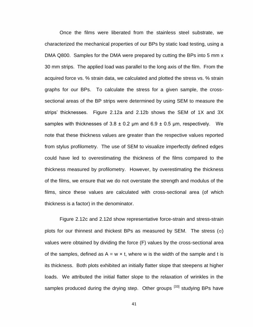
Once the films were liberated from the stainless steel substrate, we
characterized the mechanical properties of our BPs by static load testing, using a
DMA Q800. Samples for the DMA were prepared by cutting the BPs into 5 mm x
30 mm strips. The applied load was parallel to the long axis of the film. From the
acquired force vs. % strain data, we calculated and plotted the stress vs. % strain
graphs for our BPs. To calculate the stress for a given sample, the cross-
sectional areas of the BP strips were determined by using SEM to measure the
strips’ thicknesses. Figure 2.12a and 2.12b shows the SEM of 1X and 3X
samples with thicknesses of 3.8 ± 0.2 μm and 6.9 ± 0.5 μm, respectively. We
note that these thickness values are greater than the respective values reported
from stylus profilometry. The use of SEM to visualize imperfectly defined edges
could have led to overestimating the thickness of the films compared to the
thickness measured by profilometry. However, by overestimating the thickness
of the films, we ensure that we do not overstate the strength and modulus of the
films, since these values are calculated with cross-sectional area (of which
thickness is a factor) in the denominator.
Figure 2.12c and 2.12d show representative force-strain and stress-strain
plots for our thinnest and thickest BPs as measured by SEM. The stress ( )
values were obtained by dividing the force (F) values by the cross-sectional area
of the samples, defined as A = w × t, where w is the width of the sample and t is
its thickness. Both plots exhibited an initially flatter slope that steepens at higher
loads. We attributed the initial flatter slope to the relaxation of wrinkles in the
samples produced during the drying step. Other groups [33] studying BPs have

42
observed this similar relaxation behavior during tensile load to failure. In
addition, once crack formation and propagation begins the process is irreversible
if the load is removed. This suggests that BP films are not elastically inclined to
return to their original state and will lack a plastic deformation region (strain
hardening or necking). Therefore, we would expect not to see a drastic decrease
in the forces at the fracture point because the ultimate tensile strength and the
yield strength are the same as shown in figure 2.12d. The procedure used to
obtain the tensile strength and Young’s modulus of our BPs is as follows. The
ultimate tensile strength, in MPa, occurred at the samples’ fracture point, which
was at the maximum strain value in Figure 8d. The Young’s modulus was
calculated using the following equation12
12
%%100E , where σ1 and σ2
are different values of stress on the steeper linear portion of the plot and %ε1 and
%ε2 are their respective % strain values.

43
Figure 2.12. Cross section SEM images, of 1X (a) and 3X (b) buckypapers with
thicknesses of 3.8 m and 6.9 m respectively: Scale bars are (a) 3 m and (b)
2.5 m. Graphs of (c) force - % strain, F is the change in force value and % is
the change in strain value (d) stress - % strain of 1X and 3X buckypapers.

44
Table 2.1 shows the associated values for the 3X BPs that we produced.
Our values compared quite favorably to the results from other BP fabrication
techniques and for other types of carbon nanotube constituents, especially
considering that the MWCNTs of our samples were covered with a surfactant that
can attenuate the attractive interaction between pairs of nanotubes. The lower
value of Young’s modulus for sample 5 likely is a result of macro- and micro-
wrinkles in the sample originating from the drying procedure. As the sample is
loaded, these wrinkles can be relaxed with significantly less force than is needed
to dislocate the MWCNTs, so they are surmised to have a downward effect on
the slope of force-strain curve, thereby reducing the Young’s modulus. The
higher tensile strength for sample 3 compared to the other four samples cannot
be explained readily from the observed MWCNT arrangement in the BPs.
Because the samples for mechanical measurement were cut from the larger as-
liberated BPs and selected at random, it is possible that a sample from the BP
edge could exhibit different properties than those from within the center of the
BP, since the EPD behavior at electrode edges and air-liquid interfaces is
different from the EPD behavior at the center of the electrode due to fringe field
effects and possible meniscus and evaporation effects. The manifestation of
these effects in the mechanical properties of the BPs will be the subject of future
investigation.

45
Table 2.1. Comparison of our BPs to other fabrication methods.
Samples Tensile Strength
(MPa)
Young’s Modulus
(GPa)
1 10.1 3.60
2 12.5 3.38
3 27.0 3.99
4 12.7 3.3
5 10.2 2.20
Average 12.7 3.27
Table 2.2 shows the comparison of the tensile strength and Young’s
modulus of BPs in this study with those prepared by other methods. Xu et al. [19]
through a filtration method used a temperature based acid treatment to enhance
the interaction of MWCNTs, as where we used an EPD procedure.
Comparatively, our BPs exhibit greater tensile strength and Young’s modulus
values. The strongest BPs described by Xu et al had a tensile strength and
Young’s modulus of 7.5 MPa and 785 MPa respectively with an acid treatment
temperature of 110 oC. These values were considerably less than those reported
by Zhang et al. [33] who increased their BP strength by also performing acid
treatments.

46
Table 2.2. Tensile strength and Young’s modulus comparison of BPs.
Authors Constituents / Film
Type
Tensile Strength
(MPa)
Young’s Modulus
(GPa)
Zhang et al. [2] SWNTs film 10
16 71 74
0.8 1.4 2.9 5
Pham et al. [34] SWNTs BP 6.49 2.29
Xu et al. [19] MWCNTs BP 4.3 4.6 7.5 6.0 4.5
0.426 0.439 0.785 0.557 0.455
This study.[28] MWCNTs BPs 12.7 3.27
Investigations of the fracture sites of the 1X (Figure 2.13a and 2.13b) and
3X (Figure 2.13c and 2.13d) BPs provided insight into the possible mechanisms
for failure within the films. In Figure 2.13a a 1X BP films failure region is shown,
in which individual MWCNTs were extended from a randomly oriented network.
Some fraction of the nanotubes was oriented in the direction of applied load. We
considered the BPs as a multi-layered fibrous composite, [35] for which a “fiber” in
our material consists of the local network of randomly oriented MWCNTs. The
implication here is that during the application of the load, individual MWCNT
fibers began to unravel via tube-tube shearing from each other within the
randomly oriented network, producing the observed failure of the bulk BPs. As
the failure propagated across the sample, as depicted in Figure 2.13b, bridging
[36] occurred. A MWCNT bridge forms when a single MWCNT is simultaneously
connected to opposite sides of a fracture site within a film that has experienced

47
tensile loading. Figure 2.13c illustrated that several MWCNTs were bridging the
two sides of a fissure at a point of deformation in the buckypaper.
From Figure 2.13c, we perceived another failure mechanism, slip, which
we attributed to the multiple-deposition approach, which closely packs each of
the deposited layers. For our BP system, this was observed in the closely
packed multi-layered structure of the 3X BPs. This type of failure was noticeable
along both fracture sites of the 3X samples. From observations of the 1X and 3X
BPs, we concluded that the plastic deformation range increased as we fabricated
thicker films in a laminar, layer-by-layer architecture, thereby increasing the
overall strength of the buckypapers. Figure 2.13d shows the deformation that
occurred both horizontally and vertically within our multi-layered films. As the
MWCNT deposit dried onto the substrate with the voltage still applied,
densification occurred, which left minimal space between the MWCNTs layers
(for example, between the 1X and 2X layers or between the 2X and 3X layers).
In a 3X deposition, for example, the solution-phase MWCNTs that arrived at the
electrode’s surface to deposit and to adhere onto the previously cast MWCNTs
did not substantially intertwine with the network of underlying MWCNTs. This
formed nearly isolated, bulk layers of carbon nanotubes that comprised the
overall cast film. The interfaces between these 1X, 2X, and 3X layers gave rise
to the observed slip plane interfaces (Figure 2.13c).

48
Figure 2.13. SEM images of samples subjected to load to failure testing, arrows
indicate direction of applied load. (a) 1X buckypaper; scale bar 2 m (b)
unraveling (tube-tube shearing) of randomly oriented MWCNT network; scale bar
500 nm (c) 3X buckypaper; scale bar 2 m and (d) 3X failure region similar to
9(b) for layer by layer deposition; scale bar 500 nm.
Failure of these randomly distributed networks occurred when the
MWCNTs became unraveled via nanotube-nanotube shearing. The SEM images
in Figure 2.13 suggested that with each deposited layer, stress propagation
occurred in the vertical and horizontal directions, leading to the unraveling
phenomena of the nanotubes, as they were seen protruding from the bulk of the
films (Figs. 2.13b and 2.13d). In a multi-deposited buckypaper, the appearance
of parallel but staggered fracture sites suggested that stress did not propagate as
readily across the deposition interfaces. Instead, failure transpired when a

49
critical number of nanotube-nanotube failure events were realized in each
layered MWCNT network. The result was that multiple depositions engendered
greater film strength by suppressing the accumulation of failures in one region of
the film due to the random orientation between each deposited interface.
2.5. Conclusion
In this study, we have described and demonstrated a technique for the
rapid production of buckypapers by first performing EPD of MWCNTs onto
stainless steel electrodes and then liberating the film of MWCNTs using
mechanical cleavage. We have shown the capability to vary the thicknesses of
these films by using a multi-deposition scheme. Conceivably, the film
thicknesses could be tuned outside of the 1 m to 7 m range we have shown by
varying the duration of each deposition step and by varying the total number of
deposition steps. Preliminary measurement of the mechanical properties of our
BPs showed them to have an average tensile strength and Young’s modulus of
14.5 MPa and 3.3 GPa, respectively. These values compare quite favorably to
values reported for buckypapers prepared from other carbon nanotube types and
via other fabrication methods. Finally, the BPs prepared by our technique are
flexible and contain nanotubes in a random porous network, which suggest
possible use of these BPs in applications such as filtration and energy storage.

50
Works Cited
1. Wang, D., et al., Highly oriented carbon nanotube papers made of aligned carbon nanotubes. Nanotechnology, 2008. 19: p. 075609.
2. Zhang, S., et al., Solid-state spun fibers and yarns from 1-mm long carbon nanotube forests synthesized by water-assisted chemical vapor deposition. Journal of Materials Science, 2008. 43(13): p. 4356-4362.
3. Boccaccini, A.R., et al., Electrophoretic deposition of carbon nanotubes. Carbon, 2006. 44(15): p. 3149-3160.
4. Du, C. and N. Pan, Supercapacitors using carbon nanotubes films by electrophoretic deposition. Journal of Power Sources, 2006. 160(2): p. 1487-1494.
5. Mahajan, S., et al., Carbon nanotube–nanocrystal heterostructures fabricated by electrophoretic deposition. Nanotechnology, 2008. 19: p. 195301.
6. Frackowiak, E., et al., Supercapacitors based on conducting polymers/nanotubes composites. Journal of Power Sources, 2006. 153(2): p. 413-418.
7. Du, C., J. Yeh, and N. Pan, Carbon nanotube thin films with ordered structures. Journal of Materials Chemistry, 2005. 15(5): p. 548-550.
8. Kim, J.H., et al., Fabrication and electrochemical properties of carbon nanotube film electrodes. Carbon, 2006. 44(10): p. 1963-1968.
9. Futaba, D.N., et al., Shape-engineerable and highly densely packed single-walled carbon nanotubes and their application as super-capacitor electrodes. Nature Materials, 2006. 5(12): p. 987-994.
10. Pushparaj, V.L., et al., Flexible energy storage devices based on nanocomposite paper. Proceedings of the National Academy of Sciences, 2007. 104(34): p. 13574.
11. Sreekumar, T., et al., Single-wall carbon nanotube films. Chemistry of Materials, 2003. 15(1): p. 175-178.
12. Berhan, L., et al., Mechanical properties of nanotube sheets: Alterations in joint morphology and achievable moduli in manufacturable materials. Journal of Applied Physics, 2004. 95: p. 4335.
13. Skakalova, V., et al., Effect of chemical treatment on electrical conductivity, infrared absorption, and Raman spectra of single-walled carbon nanotubes. Journal of Physical Chemistry B, 2005. 109(15): p. 7174-7181.
14. Dettlaff-Weglikowska, U., et al., Effect of SOCl2 treatment on electrical and mechanical properties of single-wall carbon nanotube networks. Journal of the American Chemical Society, 2005. 127(14): p. 5125-5131.
15. Teague, L.C., et al., Effects of ozonolysis and subsequent growth of quantum dots on the electrical properties of freestanding single-walled carbon nanotube films. Chemical Physics Letters, 2007. 442(4-6): p. 354-359.
16. Gong, T., et al., Connection of macro-sized double-walled carbon nanotube strands by bandaging with double-walled carbon nanotube films. Carbon, 2007. 45(11): p. 2235-2240.
17. Wei, J., et al., Ultrathin Single–Layered Membranes from Double–Walled Carbon Nanotubes. Advanced Materials, 2006. 18(13): p. 1695-1700.
18. Ci, L., et al., Ultrathick freestanding aligned carbon nanotube films. Advanced Materials, 2007. 19(20): p. 3300-3303.

51
19. Xu, G., et al., The feasibility of producing MWCNT paper and strong MWCNT film from VACNT array. Applied Physics A: Materials Science & Processing, 2008. 92(3): p. 531-539.
20. Cooper, S.M., et al., Gas permeability of a buckypaper membrane. Nano Letters, 2003. 3(2): p. 189-192.
21. Islam, M.A. and I.P. Herman, Electrodeposition of patterned CdSe nanocrystal films using thermally charged nanocrystals. Applied Physics Letters, 2002. 80(20): p. 3823-3825.
22. Mahajan, S., et al., Structural properties of electrophoretically deposited europium oxide nanocrystalline thin films. Journal of Materials Science, 2006. 41(24): p. 8160-8165.
23. Wong, E.M. and P.C. Searson, ZnO quantum particle thin films fabricated by electrophoretic deposition. Applied Physics Letters, 1999. 74: p. 2939.
24. Maenosono, S., T. Okubo, and Y. Yamaguchi, Overview of nanoparticle array formation by wet coating. Journal of Nanoparticle Research, 2003. 5(1): p. 5-15.
25. Thomas, B., A. Boccaccini, and M. Shaffer, Multi―Walled Carbon Nanotube Coatings Using Electrophoretic Deposition (EPD). Journal of the American Ceramic Society, 2005. 88(4): p. 980-982.
26. Cho, J., et al., Characterisation of carbon nanotube films deposited by electrophoretic deposition. Carbon, 2009. 47(1): p. 58-67.
27. Hasan, S.A., D.W. Kavich, and J.H. Dickerson, Sacrificial layer electrophoretic deposition of free-standing multilayered nanoparticle films. Chemical Communications, 2009(25): p. 3723-3725.
28. Rigueur, J.L., et al., Buckypaper fabrication by liberation of electrophoretically deposited carbon nanotubes. Carbon. 48(14): p. 4090-4099.
29. Hasan, S.A., et al., Electrophoretic deposition of CdSe nanocrystal films onto dielectric polymer thin films. Thin Solid Films, 2009. 517(8): p. 2665-2669.
30. Islam, M.A., et al., Addition, suppression, and inhibition in the electrophoretic deposition of nanocrystal mixture films for CdSe nanocrystals with gamma-Fe2O3 and Au nanocrystals. Nano Letters, 2003. 3(11): p. 1603-1606.
31. O'Brien, R.W. and L.R. White, Electrophoretic mobility of a sperical colloidal particle. J. Chem. Soc., Faraday Trans., 1978. 2(74): p. 1607-1626.
32. Sarkar, P. and P.S. Nicholson, Electrophoretic deposition (EPD): mechanisms, kinetics, and application to ceramics. Journal of the American Ceramic Society, 1996. 79(8): p. 1987-2002.
33. Pham, G.T., et al., Mechanical and electrical properties of polycarbonate nanotube buckypaper composite sheets. Nanotechnology, 2008. 19(32): p. -.
34. Pham, G.T., et al., Mechanical and electrical properties of polycarbonate nanotube buckypaper composite sheets. Nanotechnology, 2008. 19: p. 325705.
35. Curtin, W.A., Dimensionality and size effects on the strength of fiber-reenforced composites. Composites Science and Technology, 1999. 60.
36. Malik, S., et al., Failure mechanism of free standing sigle-walled carbon nanotube thin films under tensile load. Phys. Chem., 2004. 6: p. 3540-3544.

52
CHAPTER 3
OPTIMIZATION OF MULTI-WALLED CARBON NANOTUBE PHOTON
ABSORBERS FOR MID-AND FAR-INFRARED STRAY LIGHT SUPPRESSION
IN SPACE INSTRUMENTATION
Chapter Overview
In this chapter, I discuss the research conducted at the National
Aeronautics and Space Administration (NASA) Goddard Space Flight Center
(GSFC) for the optimized growth of catalyst assisted chemical vapor deposition
(CVD) nanotubes for the improvement of absorption in vertically aligned (VA)
films. Films of VA-nanotubes have been shown experimentally to be excellent
absorbers close to that of unity, theoretically and experimentally [1, 2]. We
hypothesized that by optimizing the growth process we would be able to increase
film height and successively lower the density, allowing us to improve film
absorption. We describe our findings on the effects of optimization and
characterize our VA-nanotube films. We conclude by describing the effects of
the optimization process on our films.
3.1. Introduction
A Blackbody Material
In physics, a blackbody, a concept first introduced by Kirchhoff [3], is a
theoretical object that absorbs all incident light, due to the lack of transmittance
and reflection. As such, it has an appearance at room temperature which is
“super black.” The definition of this “blackness” is described by the emissivity (e)

53
which is equivalent to unity, where we define e as the ratio of radiated energy by
an object to that of a blackbody. In thermal equilibrium a blackbody emits
blackbody radiation (electromagnetic radiation) according to Planck’s Law of
radiation given by
1)/exp()(
3
32
cu 3.1
where this equation gives the relative intensity of the radiation as a function of
frequency.
Super black materials are tremendously important for optical coatings of
instruments [4] and solar energy conversion [5, 6] due to their ability to reduce
unwanted reflections and absorb stray light. Carbon is an excellent absorber
with an e of 0.8 – 0.85 [1] and is used in various materials to improve absorption.
Scientists have made advances in this area due to the importance of obtaining
super black materials. Materials such as nickel-phosphorous (Ni-P) [7], micro-
structured silicon (Black-Si) [8], silicon nano-tip (SiNTs) arrays [9] and nano-fractal
gold (gold black) [10], have all been fabricated. Recently, nanotubes have been
placed in the forefront as an inexpensive novel material which has the lowest
reflectance over a larger wavelength spectrum (UV-VIS-IR) and angles of
incidence when compared to other materials. The low reflectance is due
primarily to the interaction of light at the air – nanotube interface, caused by the
variation in the refractive index. Large jumps in the refractive index, translates
into an increase in reflection, according to Fresnel’s law given by;
2
0
2
0
)(
)(
nn
nnR 3.2

54
where n0 is the refractive index of air (n0 = 1.0003), n refractive index of other
material (in this case CNTs) and R the reflectance. Thus when the refractive
index is close to air, reflection is inhibited simply because the momentum of the
incident photon is not deterred. Currently there are two methods to reduce the
air – medium interface issue;
I. fabricate materials with a graded refractive index, and/or
II. find a material with a refractive index close to air.
Surface modified Ni-P, with its micrometer-sized features is one such
material with a graded refractive index approach. The micro-sized cavities aid in
effectively trapping photons at normal incidence, yielding a low reflectance (R =
0.16-0.18%); however, this R becomes significantly greater at larger angles (R =
4-5%) and wavelengths (R =10% at 10 m) [1]. SiNTs arrays have low
reflectance in the visible though its infrared reflectance increases linearly with
wavelength [9]. Theoretical calculations for nanotubes predicted refractive index
values of 1.01 -1.10 [11], due to their vertical alignment, nanometer rough surface
and array spacing. These intrinsic features permit a low reflectance (R = 0.03-
0.045%) [2] and an index of refraction close to that of air. While graded refractive
index materials have provided decent results, difficulty arises in the fabrication
methods and the cost of production is rather expensive and hazardous. For this
reason, CNTs are an excellent cost effective alternative and can be grown on
numerous substrates, which aligns with the goals of NASA.
Literature Review

55
The 1D allotrope of carbon is related to the 2D allotrope by a rolled-up
vector (as discussed in Chapter 1), therefore it has been standard practice to use
the optical properties of graphene to describe the optical properties of nanotubes.
The research of the scientific community is presented below in chronological
order beginning with such an investigation en route to the development and
understanding of VA nanotubes as absorbers.
Taft E. A. et al.[12] (1965): Optical properties of Graphite
Derived the complex dielectric constant for graphite by the application of
the Kramers - Kronig relation to reflectance data in the energy range to 26
electron volts (eV).
In the 0 to 9 eV range, the intra- and inter-band optical transitions involve
mainly the bands which arose from the one electron per atom, atomic
2pz orbitals extending above and below the carbon-layer planes.
De Heer W. et al.[13] (1995): Aligned carbon nanotube films: Production and
optical and electronic properties
Developed a method to produce thin films of aligned carbon nanotubes
aligned either parallel ( -aligned) or perpendicular ( -aligned) to the
surface.
Dielectric functions of the films were determined by ellipsometry. For light
polarized along the tubes ( II) the surface resembles graphite. For light
polarized along the perpendicularly ( ┴) the dielectric function from an
effective medium point of view should be a mixture of the two dielectric

56
functions of graphite, (parallel ( grII) and perpendicular ( gr┴) to the graphite
sheets).
Raman studies of aligned cross sections revealed that comparison of the
II to ┴ direction indicated stronger effective photon-phonon coupling in
the parallel direction at 1582 cm-1.
Garcia-Vidal F. et al.[11] (1997): Effective medium theory of the optical properties
of aligned carbon nanotubes
Theoretical study using effective medium theory to analyze the
experimental findings of DeHeer et al. (above).
Developed a Maxwell-Garnett approach to study the system and
demonstrated that a full electromagnetic coupling between the nanotubes
is necessary for explanation.
Lu W. et al.[14] (2000): Optical properties of aligned carbon nanotube systems
studied by the effective-medium approximation method
Comparison of Maxwell-Garnett theory 2D array model and Effective-
Medium approximation (EMA-Bruggeman’s theory) of an aligned nanotube
system based on the nanotubes described in reference [4].
Solutions for both MGT and EMA equations yielded an effective dielectric
of )1( ffs
eff for s-polarized light, where the volume fraction (f)
can be estimated by Im'Im fs
eff (where ff )1('2 ). For p-
polarized light, eff for EMA consisted of two E-field components and for
MGT one E-field component.

57
The EMA theory which is valid for densely and randomly distributed
particle systems explained the experimental data of reference [4] better
than MGT theory.
Marinopoulos A. et al.[15] (2003): Optical and Loss Spectra of Carbon
Nanotubes: Depolarization Effects and Intertube Interactions
Calculated absorption and loss spectra for 4 Å nanotubes in both random
phase and the adiabatic local density approximations.
Local field effects induced by an external field suppresses absorption
peaks rendering tubes almost transparent below 5 eV, agreeing with
experimental observations.
Intertube interactions and distances can be evaluated due to the
measurability spectroscopic quantity of the + plasmon peak.
Murakami Y. et al.[16] (2005): Polarization dependence of the optical absorption
of single-walled carbon nanotubes
Presented anisotropic optical absorption properties of SWCNTs for the
energy range of 0.5 to 6 eV, as determined by polarized optical absorption
measurements.
Polarization dependence of absorption peaks due to maxima at 4.5 eV
(Im{ ┴} and 5.25 eV (Im{ II-1} related to the optical properties of graphite.
Noted the considerable scientific disagreement for the absorption peaks at
4.5 and 5.25 eV.

58
Demonstrated that the chirality dependence of the absorption in SWCNTs
can be traced back to combined effects of the joint density of states and
the optical matrix element.
Yang Z. et al.[2] (2007): Experimental observation of an extremely dark material
made by a low-density nanotube array
Engineered low density vertically aligned multi-walled carbon nanotube
arrays to index match the vacuum, achieving low reflection.
Ultra low diffused reflectance of 1 x 10⁻⁷ measured with an integrated total
reflectance of 0.045% at = 635 nm, making it the darkest known
material.
Calculated effective index of refraction ( effn ) and absorption coefficient (
eff ) as a function of nanotube spacing as shown in Figure 3.1. At an
intertube spacing (a = 50 nm) and tube diameter (d = 10 nm), for p-
polarization an 026.1p
effn and 112.0 mp
eff , thus %02.0pR ; for s-
polarization 074.1s
effn and 19.2 ms
eff , thus %60.0sR .

59
Figure 3.1.[2] Calculated effective index of refraction and the absorption constant plotted as a function of nanotube spacing. A schematic of the nanotube array and the s and p light polarizations is displayed in the inset.
Mizuno K. et al.[1] (2008): A black body absorber from vertically aligned single-
walled carbon nanotubes
Demonstrated that vertical alignment is key component to absorption of
films.
Produced SWCNT films with near constant and near-unity emissivity of
0.98-0.99 across the spectral range of 200 nm to 200 m.
Lidorokis et al.[17] (2009): Photonics with Multi-wall carbon nanotubes arrays
Theoretically modeled CNT-based photonic crystals (2D array model)
using the finite-difference time-domain (FDTD) method, where they
propose that second order Bragg scattering resonantly redirects incident
light into the film so it is quickly absorbed.

60
For small intertube spacing of 20 - 30 nm, obtained strong Bragg
scattering and photonic band gaps in the deep UV range (25 – 35 eV).
For intermediate spacing of 40 – 100 nm, the photonic bands anti-cross
with the graphite plasmon bands resulting in a complex photonic structure
leading to reduced Bragg scattering. For large spacing >150 nm, the
Bragg gap move into the VIS and decreases due to absorption.
Lehman et al.[18] (2010): Very black infrared detector from vertically aligned
carbon nanotubes and electric-field poling of lithium tantalite
Demonstrated the practical application of water-assisted CVD grown
MWCNTs as a coating on a lithium tantalite (LiTaO3) pyroelectric detector.
A 2 nm Fe catalyst layer on top of a 20 nm Al2O3 layer was used to seed
tube growth.
Observed difference in reflection of detector and witness (Si substrate)
attributable to the detectors electrode metal and surface properties of
LiTaO3.
Bao H. et al.[19] (2010): Optical properties of ordered vertical arrays of multi-
walled carbon nanotubes from FDTD simulations
FDTD method was used to calculate the reflection, transmission and
absorption properties of VA-MWCNTs, with variations in parameters such
as intertube distance nanotube length and diameter, polarizations and
incident wavelength. Results were compared to MGT theory.

61
Absorbance at any wavelength can be fitted to )(1)( LeLA ; where is
the absorption coefficient and L tube length. Also noted that good surface
alignment can produce darker material.
The scientific contributions have demonstrated that the bulk of research has
focused mainly on theoretical modeling of these 2D VA-nanotube arrays. The
experimental research momentum has confirmed in some instances the concepts
of these theoretical models, and has focused on development of practical
applications utilizing this material.
The conventional approach to growth of nanotubes is the CVD method.
Though the growth process is not yet fully understood, (more specifically, control
of tube chirality, height and density), we are able to tune certain properties of
films, i.e. tube diameter, height and density. Nessim et al.[20] demonstrated this
tuning by controlling the timing and duration of hydrogen exposure during CVD
annealing and growth. Using this scheme, we focused growing of VA- MWCNTs
at GSFC as a replacement for Z306 paint, the standard blackening surface
treatment for spacecraft parts, in order to reduce the inherent random photon
scattering. Our goal is to be able to reproduce our film growth, with minute
differences in the reflectivity/absorption, en route to growing these films on the
components of telescopes thereby reducing stray photons. In our early
experimental endeavors, we had a wide dispersion of the reflectance data with
respect to the hydrogen exposures, as we sought optimal growth parameters.
The fabrication of homogeneous films requires several key factors, as described
in the literature and this chapter, which must be addressed; these factors include

62
the density/volume fill fraction (v.f.f.), tube length, intertube distance, surface
roughness and incident angle.
3.2. Methods
Sample Preparation
Substrates of silicon (Si) and titanium (Ti) were cleaved and machined
respectively to a dimension of 130 ± 2 square millimeters (mm2) and cleaned via
sonication in acetone followed by sonication in isopropyl alcohol and then blow
dried with an air stream. After the cleaning procedure, all samples were weighed
using a microbalance with an instrument error of ± 2 E-6 micrograms ( g). The
weighing procedure was additionally performed after physical vapor deposition
(PVD) process and CVD growth process to obtain the bulk mass of nanotubes.
This method is preferred rather than scraping or etching the film from the
substrate due to the negative implications of the latter procedures.
Physical Vapor Deposition
In order to fabricate thin films, a PVD 75 deposition system (Kurt J. Lesker
Co. USA) was used for deposition of the alumina layer (Al2O3) and iron catalyst
(Fe). 99.99% purity Al2O3 1.5 - 4 mm pieces and 99.95% purity Fe pellets with
1/8” in diameter X 1/8” in length and were purchased from Kurt J. Lesker Co.
Both materials were resistively heated, permitting thermal evaporation and
deposition onto silicon Si and Ti substrates. An initial Al2O3 layer of 60

63
nanometers (nm) was deposited followed by the deposition of the Fe layer with
various thicknesses of 2, 4, 6, 8, and 10 nm.
Chemical Vapor Deposition
Growth runs of our vertically aligned films were performed via the CVD
technique. Samples were placed into a three zone atmospheric-pressure furnace
operating at a maximum temperature of 750 oC, with a fused silica tube with an
internal diameter of 1 inch. The flow rates of the reactant gases used were; for
Argon (Ar), 980 standard cubic centimeters (sccm), which was reduced to 410
sccm with the inclusion of water (H2O) vapor; hydrogen (H2) 580 sccm; and
ethylene (C2H4) 990 sccm. During this phase of experimentation, we varied the
H2 gas flow time which consequently varied the exposure time of the heated
catalyst layer. The growth time (as determined by the duration of C2H4 feedstock
gas) remained constant at 15 minutes for multi-walled nanotube growth.
Scanning Electron Microscopy
Nanotube heights were obtained using the SEM at NASA GSFC operated
at 5kV and a Raith eLine Tool operated at 10kV at Vanderbilt University. The
film morphology and topography were characterized using high magnification
SEM.

64
Raman Spectroscopy
Raman spectra of our MWCNTs were obtained with a Horiba JOBIN-
YVON LabRam HR800 Raman spectrometer measured in the range of 100 cm-1
to 3000 cm-1 with the excitation of a He-Ne laser. Wavelengths of 632.8 (633)
nm and 784 nm were used for sample excitation.
Hemispherical Reflectance
Optical reflectance/absorption measurements were collected with a
Perkin Elmer Lambda 950 UV/VIS/NIR Spectrophotometer with an integrating
sphere operated with a monochromatic light source. The standard procedure
consisted of irradiating our samples with un-polarized light at an incident angle of
8o from the surface normal over the spectral range of 200 – 2500 nm. Detection
occurs through a photomultiplier tube for the UV/VIS range and a Peltier-cooled
lead sulfide (PbS) detector for the NIR range. For angular dependence
measurements, incident angles of 0o and 8o were used with a polarized and un-
polarized source. Baseline corrections were performed using a barium sulfate
reference sample with a calibration to a NIST standard prior to experimentation.
3.3. Growth of Vertically Aligned MWCNTs
We investigated the effects of H2 exposure time on the structure of the
nanotubes, including effects on the tube diameter, intertube distance/spacing,
density and tube length. MWCNTs, which are metallic, were more desirable for
experimentation due to their larger size and uniform optical properties. SWCNTs

65
contain an array of numerous chiralities with random distributions. Their strong
chiral dependence affects its optical properties as a result of the variations in
nanotubes types and diameter. Theoretical descriptions [11, 19] of the optical
properties of CNTs, depends on the v. f. f. which is a the ratio of our calculated
sample densities to the density of graphite, 2.2 g cm-3. The aperiodic intertube
distances and variations in tube diameters allow us to treat our films as a porous
homogeneous medium. To realize low reflectance and high absorbance from our
nanotubes, a low v .f. f., i.e., a successively lower density and longer tubes are
favorable.
The CVD technique is a widely accepted method for nanotube growth,
which includes two phases of growth during CVD;
i. the formation and reduction of the Fe catalyst
ii. the nucleation and growth of the CNTs on the catalyst particles.
Important growth parameters include catalyst thickness, reactant
temperature, reactant time, gas flow rates and growth time.
Figure 3.2 shows the CVD furnace and sample positions in (a) and in (b) the
growth steps of the MWCNTs. Figure 3.3 shows the thermal profile used for our
CVD growth treatment. Initially the furnace temperature is ramped at a heating
rate of 37.5 oC/minute followed by an annealing step. Once our annealing step
has been completed, the growth is initiated for a set time period, and then
terminated as the furnace is cooled.

66
Figure 3.2. Sketch of (a) CVD furnace at zone 2 (center of furnace) and the location of samples with respect to the directional flow of gases (Ar, Ar/H2O, H2 and C2H4). The green colored sample is a reference (with only a 5 nm Fe layer) sample present in all growth runs (b) Growth steps of MWCNTs by the CVD method.
During the initial temperature ramp, the Fe layer melts and forms clusters
which act as seeds for nanotube growth and contribute to nanotube diameters.
In the annealing phase we varied the H2 exposure time of the Fe catalyst with the
H2 acting as a vapor etchant which reduces the oxidation of the Fe catalyst prior
to nucleation and growth. Further, H2 reduces gas phase pyrolysis of the
hydrocarbons causing desorption of amorphous carbon (a-C) fragments from the
catalyst surface [20]. This step is critical in maintaining the balance between the

67
formation of a-C and crystalline CNTs. The introduction of the carbon precursor,
C2H4, enables crystalline tube orientation during the growth phase. The
introduction of H2O vapor increases the catalyst lifetime and thereby extends the
lifetime of the growth process. Recent studies [21-23] showed that the diameters
and wall count can be controlled by varying the metal catalyst thickness. To
maintain experimental control, we included a witness sample in all CVD growth
runs, with a 5 nm layer of Fe deposited onto a Si substrate. It was anticipated
that a smaller Fe layer thickness will produce longer vertically aligned nanotubes.
Figure 3.3. Thermal profile used for CVD growth of multi-walled carbon nanotubes where the variable is the H2 exposure time (flow rate of 580 sccm) relative to the introduction of C2H4 with a flow rate of 990 sccm. The carrier gas is dry Ar with a flow rate of 980 sccm (without H2O vapor) and wet Ar at 410 sccm (with H2O vapor).

68
Table 3.1. H2 exposure times and growth results. The H2 exposure times are explained as followed; (i) t-15 – H2 introduced 15 minutes prior to introduction of C2H4 (ii) t=0 – simultaneous introduction of H2 and C2H4 (iii) t+10 – H2 introduced 10 minutes after introduction of C2H4. The introduction of C2H4 is the start of the growth phase.
H2 Exposure Times (min)
t-15 t-10 t-5 t=0 t+5 t+10
Results of Growth Trials
Growth Growth Growth Growth* 1. Growth 2. No growth
No Growth
*Initial trials on the Si substrate yielded a large height variation as shown in Appendix B.
Table 3.1 shows the H2 exposures we attempted for the deposited Fe
catalyst and the results of whether those investigations yielded growth of CNTs.
With an increased H2 exposure time, we were able to grow homogeneous
vertically aligned CNTs. Nessim et. al. and references therein [20], demonstrated
that an increase of exposure time leads to catalyst coarsening. The coarsening
results in the transport of Fe via vapor phase or diffusion of Fe adatoms on the
Al2O3 surface. Thus the masses of initial small clusters are redistributed to larger
clusters, resulting in increased cluster size and spacing. When the H2 exposure
was performed after C2H4 was introduced, growth of nanotubes gave poor
results. Knowing that the thermal decomposition of C2H4 forms H2 and various
hydrocarbons (CH4, C2H6) [20], slower Fe reduction and coarsening occurs.
Accordingly the limit shown for the times t +5 min and t +10 min, is expected as
the growth of crystalline MWCNTs has been impeded. The t = 0 exposure time
which included the simultaneous introduction of H2, H2O and C2H4 reactant
gases yielded growth, however the heights and growth rates of the CNTs were
less than those grown with the t -5 H2 exposure time [Appendix B discusses our

69
results and how we arrived at this conclusion]. Additionally it was reasoned [20]
that the CNT diameters increase with increased H2 exposure time, hence the
importance of the H2 exposures for our investigation.
Based on our results in Appendix B, we selected the t -5 H2 exposure
times to conduct nanotube growths on Si substrates due to its steady growth
profile and previous reflectance performance [4]. To ensure that the t -5 exposure
time was optimal, we increased the H2 exposure times to t -10 and t -15. For
these additional exposure times, we explored the effect of catalyst thickness on
our films reflection.
Figure 3.4 shows the bulk mass in micrograms ( g) of the carbon content
(nanotubes, amorphous carbon, and graphitic carbon) for our respective catalyst
thicknesses as a function of the H2 exposure times. The Al2O3 and Fe layers
were deposited successively under the same vacuum conditions, ensuring the
accuracy of our carbon mass measurements by microbalance, less that of the Fe
and Al2O3 layers. The masses of the t -15 and t -10 exposure times show no
trend as a function of Fe layer thickness as compared to the t -5 exposure time,
which shows a linear trend for the mass as the catalyst layer increases. As
previously discussed, increased exposure time leads to coarsening and a slower
growth rate [20]. Larger Fe clusters, accumulating more C atoms, form larger
diameter MWCNT with an increased count of inner tubes. As such, the increase
in mass of the t -10 and t -15 samples are expected. In the case of the t -10 2
nm samples, the high mass count may be the result of;

70
i. submergence of Fe clusters into the Al2O3 underlayer thereby
causing the agglomeration of C atoms into a-C and CNTs.
ii. agglomeration of C atoms in addition to non-uniformity of surface
coverage.
iii. an effect of prolonged oxidation of the catalyst. However,
comparisons of CVD growths were performed on new and old
catalysts layers and showed no effects.
iv. position of the samples, as the 23 nm (74 g) and 24 nm (9091 g)
samples were in positions 1 and 2 (Figure. 3.2) respectively.
Figure 3.5 shows SEM images of both t -10 2 nm (23 and 24) samples, which
demonstrate point i above.

71
Figure 3.4. Mass of carbon for respective Fe catalyst layers for the t -15, t -10 and t -5 H2 exposure times. The masses of the t -15 and t -10 exposure times are relatively inconsistent. The t -5 H2 exposure time shows a linear trend for the mass as the catalyst layer increases.

72
Figure 3.5. SEM images of 23 nm (a) and 24 nm (b) samples displaying growth of nanotubes with the agglomeration of C atoms at the Al2O3 surface. The inset in (b) shows a higher magnification of this occurrence. The scale bars in the images are 200 nm.
The heights of our nanotubes were measured using scanning electron
microscopy (SEM). Figure 3.6 displays the averaged heights of nanotubes as a
function of the H2 exposure times. For the t -5 exposure, the nanotube heights
are approximately similar in value within error. The t -10 exposures show a linear
trend in height. The t -15 2 nm samples yielded nanotubes with the longest
lengths measured in our experiments, though this phenomenon did not translate
over other Fe layer thicknesses of the same exposure. The growth rates of the
nanotubes are initially rapid, with the presence of the H2O vapor, a weak
oxidizer, they are etched during the growth process. This may explain the
relative similarity in heights for our t -5 samples. Accounting for the effects of
prolonged H2 exposure on the Fe catalyst [20], the inconsistency of growth may
explain our t -10 and t -15 samples. Further we postulate that due to the effect of

73
CNT length on absorption, for which longer tubes have a higher absorbance [11,
19], the performance of the t -15 exposures over t -5 and t -10 exposures ought to
improve. We will discuss a method of accomplishing this below.
Figure 3.6. Heights of nanotubes (averaged) as measured by SEM for t -5, t -10 and t -15 H2 exposure times. t -5 heights are approximately the same within error, t -10 heights have a linear trend and t -15 show no trend.
From our bulk mass and height measurements, we calculated the bulk
density of our nanotubes with respect to the catalyst thickness based on the
following equation;
)( hA
MB
3.3

74
where is the bulk density in units of grams per cubic centimeters (g cm-3), M
the mass of the carbon nanotubes in units of micrograms ( g), A the cross-
sectional area in units of square millimeters (mm2) and h the height in units of
micrometers ( m). Figure 3.7 shows our bulk density calculations. Our samples
are porous in nature; the B takes into account the mass of the material which
includes the volume of the pores or void spaces (intertube spacing or periodicity).
The void spaces are crucial for improving the absorptive properties of nanotubes
[1, 2, 11, 13, 19]. The H2 exposures we employed in our experimentation was a
method for controlling the diameters [20]. Now that we have a representation of
the density we sought to correlate it to measured reflectance. A plot of the
reflectance (%R) as a function of bulk density would be expected to yield a linear
relationship based on equation 3.2. Figure 3.8 shows the %R density
relationship for our samples. The linear relationship is absent due to the 4nm
outlier for the t -5 exposure time. We found that our 4nm samples were
contaminated as shown in Figure 3.9, which resulted in higher %R values. The
striations shown in the figure appear as regions of less growth.

75
Figure 3.7. Average bulk density ( B) of nanotubes as a function of the catalyst thicknesses for t -5, t -10 and t -15 H2 exposure times. The bulk density of the t -5 exposure time is relatively linear with an R2 value of 0.98.

76
Figure 3.8. Relationship between reflectance (%R) and (a) bulk density and (b) areal density for our samples.
Figure 3.9. SEM image of contaminated 4nm sample. The striations shown in the inset caused regions of non-uniform growth, resulting in higher %R values.

77
Table 3.2 is a summary of the sample identifications (ID), iron (Fe) layer
thickness, hydrogen exposure times, bulk mass, measured nanotube heights,
calculated bulk densities and Average %R values. The %R values were
averaged over the wavelength range of 750 nm – 2500 nm, with an average of
1625 nm. Discussion and significance of these values are in the following
section.

78
Table 3.2. Sample identifications (ID), iron (Fe) layer thickness, hydrogen exposure times, bulk mass, measured nanotube heights, calculated bulk densities and Average %R values.
Sample ID Fe Layer (nm) H2 Exposure M ( g) height ( m) B g cm-3
) Average % R
Silicon 21 2 t -5 395 70.57 0.02 0.1604 ± 0.0500
Silicon 22 2 t -5 365 53.04 0.03 0.1395 ± 0.0501
Silicon 41 4 t -5 478 51.3 0.04 0.3147 ± 0.0598
Silicon 42 4 t -5 790 62.3 0.05 0.2738 ± 0.0496
Silicon 61 6 t -5 1243 47.36 0.10 0.2360 ± 0.0699
Silicon 62 6 t -5 1460 78.02 0.07 0.2139 ± 0.0720
Silicon 81 8 t -5 2502 67.96 0.14 0.2011 ± 0.0445
Silicon 82 8 t -5 2456 78.02 0.12 0.2144 ± 0.0576
Silicon 101 10 t -5 2202 54.45 0.16 0.2273 ± 0.0642
Silicon 102 10 t -5 2257 68.96 0.13 0.7507 ± 0.0836
Sample ID Fe Layer (nm) H2 Exposure M ( g) height ( m) B g cm-3
) Average % R
Silicon 23 2 t -10 74 2.07 0.14 0.7379 ± 0.0779
Silicon 24 2 t -10 9091 2.02 17.65 0.5510 ± 0.0993
Silicon 47 4 t -10 1128 19.59 0.23 0.4045 ± 0.1002
Silicon 48 4 t -10 926 11.45 0.31 0.4500 ± 0.1231
Silicon 66 6 t -10 878 20.11 0.17 0.4496 ± 0.0985
Silicon 67 6 t -10 758 14.67 0.20 0.3958 ± 0.1157
Silicon 83 8 t -10 2262 43.48 0.20 0.3943 ± 0.0791
Silicon 84 8 t -10 2699 49.43 0.21 0.3816 ± 0.0651
Silicon 104 10 t -10 2788 54.1 0.20 0.4290 ± 0.1100
Silicon 105 10 t -10 3235 58.5 0.22 0.3904 ± 0.0762
Sample ID Fe Layer (nm) H2 Exposure M ( g) height ( m) B g cm-3
) Average % R
Silicon 25 2 t -15 2118 105.2 0.08 0.2749 ± 0.0770
Silicon 26 2 t -15 2870 127.7 0.09 0.3036 ± 0.0879
Silicon 45 4 t -15 1202 22 0.21 0.3756 ± 0.0879
Silicon 46 4 t -15 1020 15.4 0.26 0.4053 ± 0.1084
Silicon 64 6 t -15 2037 56.7 0.14 0.4106 ± 0.0796
Silicon 65 6 t -15 1348 20.67 0.25 0.4671 ± 0.1070
Silicon 86 8 t -15 3490 67.8 0.20 0.4472 ± 0.0806
Silicon 87 8 t -15 3668 68.24 0.21 0.3816 ± 0.0738
Silicon 105 10 t -15 360 21.4 0.06 0.3656 ± 0.0639
Silicon 107 10 t -15 208 22.96 0.04 0.3510 ± 0.0706

79
3.4. Raman Spectroscopy
The evaluation of our nanotube purity, tube alignment and defect density
is crucial in the ability to have reproducibility of obtaining vertically aligned
nanotubes. The Raman measurements were performed at Fisk University by
Yulong Cui PhD. in Professor Arnold Burger’s group.
The Raman shift spectra for the t -5 samples are shown in Figure 3.10 for
varying catalyst thicknesses. We observe for our samples the presence of the
radial breathing mode (RBM), D -band, G -band and G’ -bands. The RBM for
MWCNTs has been related to the narrow innermost tubes [24] as well as the
presence of defects and the presence of iron catalyst[25, 26]. The D -band (1318 -
1321 cm-1) is assigned to the presence of disorder in graphitic materials. The G -
band (1577 – 1585 cm-1) corresponds to the tangential vibrations of the
hexagonally bonded carbon atoms. The G’- band (D* or 2D) is a second – order
harmonic of the D mode and is indicative of long range order in samples due to
two-phonon, second-order scattering process that results in the creation of
inelastic phonons [18]. The G’-band can be utilized to assess the purity of
MWCNTs due to the unreliability of ID/IG interpretation which stems from the
effects of carbon impurities on these intensities. The G’ –band peak has been
shown to be a more accurate alternative for measuring quality and purity[27].
Additionally, disorder can be examined using the G –band peak dispersion
over multiple wavelengths. The G peak dispersion is given by the following
equation[28];
)633784(
)()( 7846331 GIGI
nm
cmGd 3.4

80
where IG is the intensity of the G –band peaks for the 633 and 784 nm
wavelengths. The G –band peak has high dispersions in more disordered
carbons where the dispersion is proportional to the degree of disorder. Figure
3.11 shows the linear relationship of the Gd (G dispersion) as a function of the
catalyst thickness. Since the Gd increases with more disorder we anticipate that
our 2 nm t -5 samples will have improved absorption capabilities over the other
Fe catalyst layer thicknesses. This finding is confirmed below in the following
section. We also note the ID/IG ratio, which exhibits a negative slope and
supports the hypothesis that the 2 nm samples will give high performance.
These examinations based on Raman data confirm the effects of impurities on
our samples. Defects such as amorphous carbon (a-C), surface defects
(adatoms, vacancies) and the influence of pentagon and heptagon structural
defects which cause helical nanotube formation on the sp2 hexagonal lattice[18]
affect sample homogeneity and thus the absorbance properties. The theoretical
models are based on solid and hollow cylinders [11, 14, 16, 19]; as shown in Figure
3.11 the nanotubes grown confirms their helical structure. Examination of the
helical angles result in angles of 28o, 33o, 44o and 45o, which is consistent with
the finding in the literature [18]. Due to the anisotropic nature of nanotubes, the
polarization dependence will be altered for helical tubes.

81
Figure 3.10. Raman shift spectra for t -5 H2 exposure time. The radial breathing mode (RBM) is present for some of our samples and is located in the range of 230 – 235 cm-1and is typically used to calculate the diameter of single-walled CNTs. In addition we observe the presence of the D, G and G’ –band peaks with intensities in the range of ~1318-1321 cm-1, 1577-1585 cm-1 and 2600 cm-1 ,
respectively. Laser beam diameter and power were 2 m and 13 mW respectively.
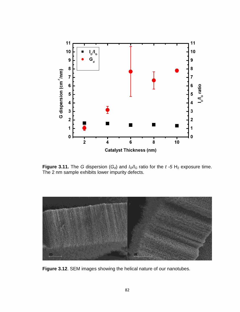
82
Figure 3.11. The G dispersion (Gd) and ID/IG ratio for the t -5 H2 exposure time. The 2 nm sample exhibits lower impurity defects.
Figure 3.12. SEM images showing the helical nature of our nanotubes.

83
3.5. Optical Absorption and Reflectance as Indicators of Performance
We used hemispherical reflectance (HR) to quantify the absorption
performance of our nanotubes grown with t -5, t -10 and t -15 H2 exposure times
as shown in Figures 3.13, 3.14 and 3.15, respectively. The t -5 exposure
samples, overall have the best performing percent reflectance (%R) and thus the
best absorptive properties. For the sample set, the %R values remains below
0.25% (R = 0.0025) from = 1250 nm. The 42 and 81 nm samples exhibit a
linear increase of %R, wavelength ( )-dependence, as increases. We will
investigate this observance further below. Our %R for the 22 nm sample is the
lowest acquired for our data shown in Figure 3.13.b as well as in Table 3.2. We
sought to compare our 2 nm samples as they gave the best performance, with
the exception of the t -10 samples. Comparison of the 2 nm %R values for the t -
5, t -10 and t -15 exposure times yielded values of 0.1395 ± 0.0501, 0.5510 ±
0.0993 and 0.2749 ± 0.0770, respectively. While the 25 nm sample has
considerably longer CNTs, its HR performance is 2 times poorer than the 22 nm
sample. Considering its height and density, the nanotubes are 2 times longer,
while the density is ~3.4 times greater than our best performers. We suggest
that these factors affects the surface roughness, longer tubes exhibit increased
irregularity at the air-nanotube interface and intertube spacing which is critical for
effective photon trapping.
Examination of the 24 nm sample by SEM (Figure 3.9), which has the
shortest CNTs measured, explains its poor performance. Further, the extremely
high density is a result of a-C present in our samples which increased the

84
reflectance and caused -dependence. As a final point, the nanotube heights
and alignment are important factors that contribute to higher absorbance[1]
allowing reflection from the bottom surface to become weaker [19].
From our averaged %R data we calculated the emissivity of our samples.
Ideally, the emissivity should be wavelength ( )-independent and unity across a
large spectral range. For our case we are observing the near IR spectrum from
750 to 2500 nm (1625 nm - averaged value). As photons interact with the
nanotubes, several mechanisms such as reflection (R), transmission (T) and
absorption (A) transpires simultaneously. The sum of these three optical
mechanism components is given by,
1ATR 3.5.
As shown, our material is highly absorptive which means we can assume that the
transmission component is accordingly minor, effectively negligible (0).
Furthermore from Kirchhoff’s radiation law we find that;
e 3.6
where e is the emission coefficient or emissivity and is the absorption
coefficient or absorptivity. It states that the emissivity of an object is equal to the
absorptivity and thus the absorptivity is equal to one in thermal equilibrium.
Setting T = 0 and substituting e = A, from equations 3.5 and 3.6 respectively, we
obtain the equation to calculate our emissivity;
Re 1 3.7.
We calculated the emissivity of our t -5 and t -15 2 nm samples as they had the
lowest %R values in our experimentation. We obtained values of 0.9984,

85
0.9986, 0.9973 and 0.9970 for 21, 22, 25 and 26, respectively which are fairly close
to 1 and demonstrate the relative closeness of nanotubes to being a blackbody.
UV Peak at 275 nm
Our analysis thus far has focused on the near IR spectrum. We now focus
on the UV spectrum (200 – 400 nm), more specifically, the UV peaks located at
~275 nm (~4.5 eV). These peaks originate from the optical properties of
graphite. As previously stated, graphite is birefringent, thus its dielectric function
consists of two components, the o and e, which correspond to ordinary and
extraordinary rays in that order (hence CNTs are birefringent and anisotropic).
.As a nanotube forms the 1D structure from 2D graphene by the rolling vector,
the nanoscale diameter causes quantization of the circumferential wave vectors,
creating strong divergences in the electronic density of states (Van Hove
singularities) which formulate discrete energy levels or sub-bands [29]. The
presence of this peak has been shown to be polarization dependent [11] and
consistent with reports for both random and aligned SWCNTs and MWCNTs [16].
The peak is attributed to several factors that include plasmon (4.2-4.5 eV)
surface and bulk plasmon excitations (5.2 eV), plasmon along tube axis, and
pristine samples containing a-C (5.2 eV).
Additional information, such as a quantitative index for nanotube
alignment, intertube spacing and v.f.f. (both relate to density), relating our
samples to o and e of graphite, can be extracted for a range of . Two
theoretical approaches have been widely used to translate the properties of

86
graphite onto nanotubes, the Maxwell-Garnett (MG) approximation [11] and
effective medium theory (EMT) [14], to calculate the effective dielectric constants
of nanotubes ( eff). However, the EMT was found to more closely fit experimental
data. In order to comprehend eff, we first acknowledge that our material is
homogeneous and electromagnetic radiation affects its permittivity. From
Maxwell’s equations, we have
PED fp 3.8
where D is the electric displacement, fp the permittivity of free space, E the
electric field and P the polarization field. The polarization field, P, is given by;
EP fp 3.9
where is the electric susceptibility. Then by combining equations 3.8 and 3.9,
we obtain the expression;
fprfpfpfp EEED )1( 3.10
where r is the relative permittivity.
For nanotubes the eff is given by the following equations for p- and s-
polarizations respectively;
)()(
)(
21212
212
2fLL
feff (MG) 3.11
0)(
)()1(
)(
)(
2
2
1
1
effeff
eff
effeff
eff
Lf
Lf (EMT) 3.12
)1( ffs
eff(MG & EMT, s- polarization) 3.13

87
where 1 is eo
for p- polarization, o for s- polarization, 2 the dielectric
constant of air, L is the depolarization factor (for p=1/2, and for s= 0) and f the
v.f.f.
Thus far, for our UV peaks, we can conclude that the reflectance values of
our best performers (Figures 3.13.a and 3.15.a – 2 nm samples) correspond to a
lower density and lower reflectance. In Figure 3.14.a, the 2 nm sample peak is
also low this is why further analysis is necessary. In order to fully obtain
quantitative information we chose to perform the Kramers-Kronig relation
analysis on our %R data for select samples (Chapter 4).
Figure 3.13. (a) Shows the peak located at 275 nm (4.5 eV) in the ultraviolet spectrum (UV). (b) Measured hemispherical reflectance of t -5 exposure time (lowest averaged reflectance showed these as our best samples) for the near infrared (IR) spectrum.

88
Figure 3.14. (a) Shows the peak located at 275 nm (4.5 eV) in the ultraviolet spectrum (UV). (b) Measured hemispherical reflectance of t -10 exposure time (best performing samples) for the near infrared (IR) spectrum. The 24 nm sample
shows the onset of -dependence.
Figure 3.15. Measured hemispherical reflectance of t -15 exposure time (best performing samples) for the near infrared (IR) spectrum. Inset shows the peak located at 275 nm (4.5 eV) in the ultraviolet spectrum (UV).

89
3.6. Conclusion
In summary, we have investigated the growth of MWCNTs under varying
H2 exposure times, t -5, t -10 and t -15. For our CVD growth we found that the t -
5 H2 exposure time yielded consistent growth results in addition to having the
lowest %R (<0.25%). Measurements of our sample masses and nanotube
heights allowed for calculation of the respective bulk densities of our samples;
the associated effects on the film properties such as absorption were
investigated. Raman spectroscopy was utilized to examine our film purity and
defect content. The Gd showed that our t -5 2 nm samples had fewer impurities.
Our %R data showed that the t -5 H2 exposures yield the most desirable
absorbance for both of our 2 nm films. We calculated that our best sample
absorbs 99.86% of light. We were able to calculate from our reflectance
data using the Kramers-Kronig relations. Furthermore, the K-K relations allowed
us to calculate the optical properties of our material. Added research is
necessary for this aspect of the research as the extrapolation points must be
selected carefully. The Im and Re values confirmed observations made by
SEM and Garcia-Vidal [11]. Finally, we were able to show the effect of angular
dependence on specular and diffuse reflectance.

90
Works Cited
1. Mizuno, K., et al., A black body absorber from vertically aligned single-walled carbon nanotubes. Proceedings of the National Academy of Sciences, 2009. 106(15): p. 6044.
2. Yang, Z.P., et al., Experimental observation of an extremely dark material made by a low-density nanotube array. Nano Letters, 2008. 8(2): p. 446-451.
3. Kirchhoff, G., Uber den Zusammenhang zwischen Emission und Absorption von Licht und. Wärme. Monatsberichte der Akademie der Wissenschaften zu Berlin, 1859: p. 783-787.
4. Hagopian, J.G., et al. Multiwalled carbon nanotubes for stray light suppression in space flight instruments. in Proceedings of SPIE. 2010: SPIE.
5. Dang, X., et al., Virus-templated self-assembled single-walled carbon nanotubes for highly efficient electron collection in photovoltaic devices. Nature Nanotechnology. 6(6): p. 377-384.
6. Camacho, R., et al., Carbon nanotube arrays for photovoltaic applications. JOM Journal of the Minerals, Metals and Materials Society, 2007. 59(3): p. 39-42.
7. Wang, Y., et al., Investigation of the structure and the physical properties of nickel-phosphorus ultra-black surfaces. Applied Physics A: Materials Science & Processing, 2008. 90(3): p. 549-553.
8. Maloney, P.G., et al., Emissivity of microstructured silicon. Applied Optics. 49(7): p. 1065-1068.
9. Huang, Y.F., et al., Improved broadband and quasi-omnidirectional anti-reflection properties with biomimetic silicon nanostructures. Nature Nanotechnology, 2007. 2(12): p. 770-774.
10. Zhao, W., et al., Fabrication, characterization and application of gold nano-structured film. Electrochemistry communications, 2006. 8(5): p. 773-778.
11. Garcia-Vidal, F., J. Pitarke, and J. Pendry, Effective medium theory of the optical properties of aligned carbon nanotubes. Physical Review Letters, 1997. 78(22): p. 4289-4292.
12. Taft, E.A. and H. Philipp, Optical properties of graphite. Physical Review, 1965. 138(1A): p. A197.
13. deHeer, W.A., et al., Aligned carbon nanotube films: production and optical and electronic properties. Science, 1995. 268(5212): p. 845.
14. Lü, W., J. Dong, and Z.Y. Li, Optical properties of aligned carbon nanotube systems studied by the effective-medium approximation method. Physical Review B, 2000. 63(3): p. 033401.
15. Marinopoulos, A., et al., Optical and loss spectra of carbon nanotubes: depolarization effects and intertube interactions. Physical Review Letters, 2003. 91(4): p. 46402.
16. Murakami, Y., et al., Polarization dependence of the optical absorption of single-walled carbon nanotubes. Physical Review Letters, 2005. 94(8): p. 87402.
17. Lidorikis, E. and A.C. Ferrari, Photonics with multiwall carbon nanotube arrays. ACS Nano, 2009. 3(5): p. 1238-1248.
18. Lehman, J.H., et al., Evaluating the characteristics of multiwall carbon nanotubes. Carbon, 2011. 49: p. 2581-2602.
19. Bao, H., X. Ruan, and T. Fisher, Optical properties of ordered vertical arrays of multi-walled carbon nanotubes from FDTD simulations. Optics Express, 2010. 18(6): p. 6347-6359.

91
20. Nessim, G.D., et al., Tuning of vertically-aligned carbon nanotube diameter and areal density through catalyst pre-treatment. Nano Letters, 2008. 8(11): p. 3587-3593.
21. Chakrabarti, S., et al., Number of walls controlled synthesis of millimeter-long vertically aligned brushlike carbon nanotubes. The Journal of Physical Chemistry C, 2007. 111(5): p. 1929-1934.
22. Hofmann, S., et al., Effects of catalyst film thickness on plasma-enhanced carbon nanotube growth. Journal of Applied Physics, 2005. 98: p. 034308.
23. Yamada, T., et al., Size-selective growth of double-walled carbon nanotube forests from engineered iron catalysts. Nature Nanotechnology, 2006. 1(2): p. 131-136.
24. Jantoljak, H., et al., Low-energy Raman-active phonons of multiwalled carbon nanotubes. Applied Physics A: Materials Science & Processing, 1998. 67(1): p. 113-116.
25. Donato, M., et al. Aid of Raman spectroscopy in diagnostics of MWCNT synthesised by Fe-catalysed CVD. 2007: IOP Publishing.
26. Santangelo, S., et al., Low-frequency Raman study of hollow multiwalled nanotubes grown by Fe-catalyzed chemical vapor deposition. Journal of Applied Physics, 2006. 100: p. 104311.
27. DiLeo, R.A., B.J. Landi, and R.P. Raffaelle, Purity assessment of multiwalled carbon nanotubes by Raman spectroscopy. Journal of Applied Physics, 2007. 101: p. 064307.
28. Ferrari, A.C. and J. Robertson, Raman spectroscopy of amorphous, nanostructured, diamond–like carbon, and nanodiamond. Philosophical Transactions of the Royal Society of London. Series A: Mathematical, Physical and Engineering Sciences, 2004. 362(1824): p. 2477-2512.
29. Saito, R., G. Dresselhaus, and M.S. Dresselhaus, Physical Properties of Carbon Nanotubes. Imperial College Press, 1998.
30. Lucarini, V., Kramers-Kronig relations in optical materials research. Vol. 110. 2005: Springer Verlag.

92
CHAPTER 4
DETERMINATION OF OPTICAL PROPERTIES AND EFFECTS ON FILM
PERFORMANCE
4.1. Experimental Improvement of Reflectance
In this experiment, samples were plasma etched with oxygen (O2) for 10
seconds at 100 Watts, removing approximately 10-15 nm from the top layer. We
choose samples from an earlier group that demonstrated a profound linear -
dependence in addition to -independence. The t =0 and t -5 exposure samples
have a Fe catalyst layer of 8 nm. The removal of the top layer of randomly
oriented bridge-like nanotubes ought to increase the absorption of the films. This
increase in absorption would be a result of an increase in the available void
spaces and reduction in surface scattering which would encourage light trapping
within the material. Further, it will provide an improvement at the air-nanotube
interface, reducing the refractive index. Figure 4.1 a and b displays our %R data
for two measured samples before and after O2 plasma etching. The results
indicate for the t =0 sample, that the process did not improved the overall
reflectance; rather it degraded the film performance. At the longer wavelengths
(>2100 nm) %R seems unchanged though this may be due to experimental error.
In the 950 to 1750 nm range, the %R degraded by an average of 50%. In the UV
range we notice a shift in the peak and a reduced magnitude. However, despite
these results, the -independence is unchanged.

93
Figure 4.1. Measured hemispherical reflectance of (a) t =0 and (b) t -5 exposure times before and after O2 plasma etch for an 8 nm Fe catalyst layer growth on silicon. The UV-VIS-NIR spectrum is plotted. The UV peaks are located at 275 nm (4.5 eV), though there is a shift to higher wavelength (lower energy/frequency) for t =0. The reflectance increases linearly after plasma etching for the t -5 sample, an approximate five-fold increase.
In Figure 4.2 we observe the SEM image showing the associated regions
of nanotube structures from the substrate to the surface. Due to the difference in
nanotube structure and alignment, these regions contain varying indexes of
refraction.

94
Figure 4.2. SEM image of CNTs with a height of ~ 35 m. Region I is the surface of the aligned nanotubes which exhibit bridge-like interconnections. Region II shows highly aligned nanotubes with helical growth and Region III is the base where growth begins.
Region I is the first region and is located at the air-CNT interface and
consists of randomly aligned nanotubes with bridge-like CNT connections. The
random surface encourages increased diffuse scattering events along the tubule
axes [1]. Additionally, these surface structures decrease the void spaces of the
aligned helical nanotubes.
Light-photon

95
Region II contains vertically-aligned helical nanotubes. The helical nature
is due to pentagon and heptagon defects [2] along the sp2 structures. These
tubes due to their angular nature and length allow for the reflectance,
transmission and absorption of light in the film. For our purpose, removal of the
region I layer and exposure of region II should further improve our films
absorbance by lowering the refractive index.
Region III, the final region, contains more aligned nanotubes. However,
the nanotubes are considerably short and are close to the substrate. At this
height the effects of absorption are reduced due to the limited path for photons to
travel. The length effect is also reduced such that we expect the reflectance to
increase. This increased reflection from the substrate is a direct result of a
glossy surface. Based on these observations we attempted to remove or reduce
the thickness of region I, and expose region II.
Figure 4.3 (a, b, c and d) show the SEM images of samples before and
after the O2 etch for t =0 and t -5 sample respectively. For the t =0 sample, we
observe the removal of the surface (region I), mentioned earlier and an
improvement in the void spaces (Figure 4.3.c). We also notice graphitic
remnants from the etch process. It is possible that these graphitic remnants are
the cause for the observed increase in %R (Figure 4.2.a).

96
Figure 4.3. SEM images of (a) t =0 before O2 plasma etch (b) t -5 before O2
plasma etch (c) t =0 after O2 plasma etch and (d) t -5 after O2 plasma etch. Insets in (a) and (b) are higher magnifications of film. Scale bars are 200 nm, for regular and insets.
For the t -5 sample, the plasma etch removed the surface diffusive
scattering of the bridge-like surface exposing the nanotubes below. Figure 4.3 (b
and d) show the SEM images for this sample. In Figure 4.3.d the surface
appears as a uniform film with relatively low void spaces. It should be noted that
even though the contrast of the SEM shows topologically where the voids are
located, it cannot ascertain the depth. The effect of the linear -dependence is
worsened as depicted in Figure 4.2.b due to the lack of void spaces in the
nanotube film. Additionally, since the nanotubes are more closely packed
without the random layer, the density of the material should increase.

97
4.2. Wavelength-Dependence Mechanisms of Reflection
We conducted additional experiments to comprehend why we observed
the linear increase in the reflectance ( -dependence) of our samples in the
infrared region. Our HR set-up consisted of two sample mounts at an angle of
incidence of 8o from the normal and 0o to examine any changes in our
reflectance data. We selected two samples from an earlier growth group which
exhibited this phenomena (as the optimization improved this phenomena
decreased). Figure 4.4.a and 4.4.b shows the graphs of a t =0 and t -5 8 nm Fe
catalyst layer sample. In Figure 4.4.a shows that for both incident angles, the
reflectance spectrum is unchanged. Figure 4.4.b, we observed that the
reflectance increased linearly at ~1700 nm for the 8o angle of incidence.
However, at the normal, 0o we immediately observed the absence of this linear
increase. In order to confirm whether this was indeed due to -dependence we
measured a sample with -independence.
We explain this phenomenon as follows: our data recorded the total
reflectance (RT) from our sample, which is all of the reflected light from the films
surface. RT is composed of two components, specular (RS) and diffuse (RD)
reflectance. The surfaces of the nanotube are rough on the nanometer scale,
where photons are scattered in both forward and backward directions. As a
result they are an excellent diffuse surface. At an incidence of 0o the beam is
reflected 180o off the nanotube surface, expunging the RS component, leaving
solely the RD. We hypothesize that at 8o, the RS component is responsible for
the -dependence. Hence, the optical reflectance mechanism fluctuates from RD

98
to RS as increases. RS may be caused by the dense electron clouds below the
diffuse layer as the nanotubes act as a bulk material with little intertube spacing.
Figure 4.4. Measured hemispherical reflectance for (a) t =0 Si 8 nm catalyst thickness at 0o and 8o angles of incidence (b) t -5 Si 8 nm catalyst thickness at 0o and 8o angles of incidence. In (b) we observe the absence of the specular component, suggesting that the linear wavelength-dependence is a component of specular reflection.
4.3. Kramers-Kronig Relations
The K-K relations describe the fundamental connection between the real
(Re) and imaginary (Im) parts of linear complex optical functions that exhibit light-
matter interaction phenomena [3]. In reflectance spectroscopy, K-K couples the
measured reflectance and phase of the reflectivity allowing retrieval of the phase
and the ability to extract quantitative information, such as the refractive index, N
( ) and complex dielectric function, eff ( ). To obtain the optical constants,
reflectance is commonly measured at normal incidence and then followed by
dispersion relations to retrieve the phase, ( ). For our measurements we
utilized angle of incidence of 8o, which is near normal, thus considering it to be
0o.

99
From Fresnel’s law, the complex reflectivity, r ( ), at the boundary
between sample and vacuum is given by,
)(1)(
)(1)(
1)(
1)()(
i
i
N
Nr 4.1
where is the frequency in eV, the index of refraction (Re), i a complex
variable and is the extinction coefficient (Im). We obtain,
*)]()[()()(2
rrrR 4.2
In polar coordinates the complex reflectivity is expressed as,
)()()( ieRr 4.3
Such that,
)()(ln)(ln iRr 4.4
If we perform of a Hilbert transform to equation 4.4, we can relate the real and
imaginary parts as,
')'(ln2
)(0 2'2
dR
P 4.5
In this equation for the phase of complex reflectivity, P is the principle value
integral.
In order to perform the principle value integration in equation 4.5, we first
needed to smooth our reflectance data. We must also extrapolate the data down
to = 0 and out to = ∞. The principle value requires that the function and its
derivative be continuous. In order to extrapolate to zero we use the simple
function,

100
2
2
11)()(o
o arr 4.6
where o is the lowest frequency point at which data was taken, f ( o) in the
reflectance at that point and a is the chosen to give a continuous derivative. To
extrapolate to infinity, we use
))()(1(
)()(
22
0
22
0
2 ba
rr
o 4.7
where o is the highest frequency at which there is data, f ( o) the reflectance at
that frequency, a is determined by requiring a continuous slope. The additional
term is added to yield a more convergent integral and to allow us to examine the
sensitivity to how rapidly we continue f ( ) to zero.
In Figure 4.5 (a and b) we show the smoothed data and the extrapolations
for two cases. We examine the t -5 Si8 sample before and after the O2 plasma
etch. Note, we perform two extrapolations in Figure 4.5.a. We use these in the
K-K relations to generate the phase of r ( ), ( ), shown in Figure 4.6. We
observe that the extrapolation of to ∞ does not have a great effect on the data
which is continued downward toward zero.
The phase, ( ) is not something for which there is any great intuition.
Given r ( ) we can use equation 4.1 to obtain the index of refraction, N ( ), both
its real and imaginary components. Further the susceptibility ( ) can be found
from
)()(
No
4.8

101
In Figure 4.6 we observe the plots of ( ) as calculated from the
dispersion relation. We can compare our value for Im ( ) to that calculated by
Garcia-Vidal et al[1]. We observe similar -dependence and similar magnitudes.
For our sample, we observe the shift of the UV peak from high to low energy. At
the higher energy the nanotubes have more intertube spacing, however at the
lower energies the nanotubes are in very close contact. Further we can surmise
that out nanotube diameters are much larger than those in Garcia-Vidal. Thus
we believe this approach is reasonable and yields ( ). The imaginary
components of ( ) are a clear measure of a materials absorbance. Thus using
the K-K dispersion relations could help assess influence of a material at
suppressing scattered light.
Unfortunately, the application of equation 4.5 to our other measured
reflectance data has proven problematic. The same calculation as used for the
above two cases yields N ( ) and ( ) with unphysical imaginary components.
This would imply an exponentially increasing wave on the light entering the
medium. Others [4-7] have found similar difficulty and have traced the problem to
the utilization of a long r in the dispersion integral. The dispersion relation is
not valid if r ( ) has a zero in the upper half plane. Several suggestions have
been made to circumvent this problem. Whether their modified approach can be
used to handle the data taken here warrants further investigation.

102
Figure 4.5. Smoothed reflectance data for a t -5 Si 8 nm catalyst thickness and the extrapolations used (a) before plasma etch and (b) after plasma etch.
Figure 4.6. Phase data for a t -5 Si 8 nm catalyst thickness (a) before plasma etch and (b) after plasma etch.

103
Figure 4.7. Calculated ( ), with real and imaginary components for t -5 Si 8 nm
catalyst thickness. (a)Re ( ) before plasma etch (b) Re ( ) after plasma etch
(c) Im ( ) before plasma etch (d) Re ( ) after plasma etch.
4.5. Conclusion
We calculated that our best sample absorbs 99.86% of light. We were able to
calculate from our reflectance data using the Kramers-Kronig relations.
Furthermore, the K-K relations allowed us to calculate the optical properties of
our material. Additional research is necessary for this aspect of the projrect as
the extrapolation points must be selected carefully. The Im and Re values
confirmed observations made by SEM and Garcia-Vidal [1]. Finally, we were able
to show the effect of angular dependence on specular and diffuse reflectance for
our samples.

104
Works Cited
1. Garcia-Vidal, F., J. Pitarke, and J. Pendry, Effective medium theory of the optical properties of aligned carbon nanotubes. Physical Review Letters, 1997. 78(22): p. 4289-4292.
2. Lehman, J.H., et al., Evaluating the characteristics of multiwall carbon nanotubes. Carbon, 2011. 49: p. 2581-2602.
3. Lucarini, V., Kramers-Kronig relations in optical materials research. Vol. 110. 2005: Springer Verlag.
4. Smith, D.Y., Dispersion relations for complex reflectivities. JOSA, 1977. 67(4): p. 570-571.
5. Smith, D. and C.A. Manogue, Superconvergence relations and sum rules for reflection spectroscopy. JOSA, 1981. 71(8): p. 935-947.
6. King, F.W., Dispersion relations and sum rules for the normal reflectance of conductors and insulators. The Journal of Chemical Physics, 1979. 71: p. 4726.
7. Plaskett, J. and P. Schatz, On the Robinson and Price (Kramers—Kronig) Method of Interpreting Reflection Data Taken through a Transparent Window. The Journal of Chemical Physics, 1963. 38: p. 612.

105
CHAPTER 5
CONCLUSIONS & FUTURE WORK
In this dissertation we have demonstrated the applicability of the
electrophoretic deposition (EPD) technique to assemble thin films of carbon
nanotubes (buckypapers). We suspended the MWCNTs in an aqueous media in
order to facilitate deposition onto a stainless steel substrate. We demonstrated
and effective method to remove the film once deposited and termed this the
“mechanical cleavage” technique. The random porous networks of nanotubes
were comparable to other BPs fabricated by alternate techniques in both its
Young’s modulus and Tensile strength.
Furthermore we have addressed a direct technological application using
MWCNTs for NASA grown via the chemical vapor deposition (CVD) method.
Due to their vertical alignment, films of nanotubes have come extremely close to
the theoretical emissivity of a blackbody. We investigated various H2 exposure
times to find consistent growth parameters for optimal absorption performance.
By varying the exposure times we were able to control, within experimental
reason, the factors important to nanotube absorption such as height, density,
v.f.f., intertube spacing and incident angle. We developed a technique to
measure the bulk density of our samples. The optical properties of a few
samples were analyzed using the Kramers-Kronig relations and yielded
quantitative and qualitative information on our samples.

106
To this end, the research discussed in this dissertation should be explored
further. En route to achieving uniform films via CVD, several exciting research
questions remain. For instance, understanding the effects of Ostwald ripening
and utilizing this phenomenon may open a new understanding of growth
termination and catalyst-underlayer adhesion. Another idea follows from the O2
plasma etch trial. If researchers are able to effectively remove the randomly
oriented nanotube surface then achieving a near perfect blackbody is in sight, as
well as solar and thermal conversion efficiencies. We began an analysis using
the K-K relations and found that they accurately retrieve intrinsic material
constants. Further investigation of our samples is necessary, especially in the
mid- to far-infrared spectrum. I believe this would aid in NASA’s goal to replace
its existing coating material with nanotubes.

107
APPENDIX A
ELECTROPHORETIC DEPOSITION THEORY
DLVO Theory
Derjaguin, Landau, Verwey and Overbeek (DLVO) theory, combines the
effects of attractive and repulsive interactions between two particles in a system.
The overall stability of the system depends on the interaction between the
individual particles in the suspension [1]. Descriptions of these interactions in the
suspension are in terms of the van der Waals attraction (UVdW) and electrostatic
repulsion (Uelect). From these mechanisms acting in a dispersed system, we can
postulate whether the particles will agglomerate or coagulate. To avoid particle
agglomeration, a high electrostatic repulsion due to high particle charge is
required. For instance, during the formation of the deposit, the particles come
closer to each other with increasing attractive force. If the charge on the particle
is low, the particles will coagulate regardless of inter-particle spacing. This leads
to deposits that are more porous in nature. In contrast, if the particles have a
higher surface charge during deposition, they will repel each other, occupying
positions that lead to a higher packing density [2].
If we examine a negatively charged MWNT in its colloidal medium
surrounded by both positive and negative ions and water, as depicted in Figure
A.1, there will be a fixed layer of positive ions at the surface. This layer is the
stern layer. Outside this stern layer is a diffuse layer of counter ions, in which a
reduction of positive ions decreases with increasing distance from the MWNT.

108
Formation of the diffuse layer occurs from free ions in the medium/system under
the influence of electric attraction and thermal motion [1]. The diffuse layer
electrically screens the stern layer. Both the stern and diffuse layers make up
the double layer. The boundary at the interface of the diffuse layer and bulk
medium (suspension) is the slipping plane. Within this region, the MWNT acts as
a single entity when a force is applied, inducing the motion of MWNT and the
double layer. The potential at this boundary is the zeta potential (refer to section
A for the value). This potential determines the particles velocity v by which they
move under the influence of the applied electric field E and the electrophoretic
mobility given by
E
. (1)
The relationship of the zeta potential and the electrophoretic mobility is
given by the Smoluchowski equation [1]
r0 (2)
where 0 is the permittivity of vacuum, r is the relative permittivity of solvent, and
the solvent viscosity. Thus, the mobility of the particle depends linearly on the
dielectric constant of the fluid, the zeta potential and the potential gradient and is
inversely proportional to the fluid viscosity.

109
Figure A.1. Schematic of double layer surrounding MWNT as two parts; the inner region where ions are strongly bound is the stern layer (a), the outer region where ions are less firmly associated is the diffuse layer (b) both regions comprise the double layer (a and b). The diffuse layer contains a boundary known as the slipping plane, where the particle (MWNT) acts as a single entity. The potential at this boundary is the zeta potential.

110
In the colloidal suspension, we assume Na+ is one of the free ions in the
system due to the proprietary surfactant present on our nanotubes. This
assumption is based on the EDS scans. Neglecting all but the electrostatic and
the van der Waals forces and treating them as separable entities, DLVO theory
allows for a description of colloidal suspensions [3].
The combination of UVdW and Uelect describes the total interaction energy
(UT) of the suspension. At nanometer distances, the attractive force is due
primarily to the van der Waals interaction, which is a result of fluctuating electric
dipole effects present in the suspension. Van der Waals attraction follows the
power law whose strength varies with the Hamaker constant (AH) and a
geometrical factor. Typically, spherical bodies represent the geometry for
particles in colloidal suspensions. For our MWNTs, rigid cylindrical bodies are
used for the approximation of the van der Waals potential. We express their
interactions as a function of their separation distance and orientation. The two
orientations of focus are parallel and perpendicular. In the case of two infinitely
long thin cylinders far apart where L >> z, the equation is given by [3]:
5
21
8
3
z
AAAU H
vdW
(3)
4
21
2 z
AAAU H
vdW
(4)
where AH is the Hamaker constant, A1, A2 the fixed cross-sectional areas and z is
the center-to-center separation as shown in Figure A.2. In addition, we can
express them as two infinitely long cylinders near contact, given by [3]:

111
2/1
2/324R
l
AU H
vdW
(5)
l
RAU H
vdW
6
(6)
where R is the fixed radii of the MWNTs and l is the variable surface separation
where l << R, as demonstrated in Figure A.3.
The Hamaker constant relates to the dielectric properties of the MWNTs
and the intervening space. Theoretical estimates have been reported in the
literature for the Hamaker constant of CNTs, which is approximated as AH = 6 x
10-19 J (3.744 eV) [4].

112
Figure A.2. (Top). Infinitely long cylinders whose orientation is perpendicular and separation distance far apart, z coressponds to the minimal center-to-center separtion, A1 and A2 are the fixed cross-sectional areas per unit length. (Below). Infinitely long thin parallel cylinders.
4
21
2 z
AAAU H
vdW
5
21
8
3
z
AAAU H
vdW

113
Figure A.3. (Top). Infinitely long, parallel circular cylinders with fixed radii R and near contact where the variable surface separation l << R. (Below). Infinitely long perpendicular cylinders near contact.
l
2
R
2
R
2/1
2/324R
l
AU H
vdW
l<
<R
2
R l
2
R
l
RAU H
vdW
6
l<<
R

114
A graph of the van der Waals energy vs. center-to-center separation for
these rigid fixed bodies of parallel and perpendicular pairs of CNTs is shown in
figure A.4. The van der Waals energy was calculated using the Hamaker
constant (~ 3.744 eV) value. For the length of the MWNTs 250 nm was taken as
a rough approximation. As the center-to-center, separation approaches zero, the
magnitude of the van der Waals forces increases. These calculations suggest
stronger inter-particle binding for CNTs that are parallel.

115
Figure A.4. Plot of the van der Waals potential energy vs. center-to-center separation between rigid CNTs of varying diameters for equations (3) and (4). Nanotubes aligned in a parallel orientation (top) and nanotubes aligned perpendicularly (bottom).
Equation (7) is the representation of the coulomb interaction of the
aqueous dispersed MWNTs:
0
2
24 D
C
eRU
(7)

116
where R is the radius, -1 the Debye screening length, ε0 the permittivity of free
space and the relative permittivity and D is the inter-tube spacing. In colloidal
suspensions, the Debye length controls the range of the double layer interaction
with other particles. In order to derive this expression, there are a few
assumptions one makes. First, we must approximate the charge on the surface
of the MWNTs. To determine this value, we solve the mobility equation for the
charge number (Z):
hR
Ze
6 (8)
where Rh is the hydrodynamic radius of the MWNT and the viscosity of the
suspension at room temperature. From earlier experiments, we determined the
value of the mobility for our MWNT solution, as measured by dynamic light
scattering, to be -3.2 10-4 cm2 V-1 s-1. Before we proceed with the solution of
equation (2), we must find a solution for the existing unknown value of Rh. The
expression for the hydrodynamic radius is equation (3); [5]
212ln3
ch
DR
(9)
where c (25 nm) the outer diameter of the
nanotube. Solving this equation for a fixed rigid MWCNT, we arrive at a value of

117
116 nm for Rh. Plugging this value into equation (8), we obtain a value of 438 for
the charge number (Z) on the surface on the nanotubes.
Now that we have a value for surface charge on a MWCNT, we proceed to
derive the force F (F = - dU/dr) between two MWCNTs surfaces. The force
between two spheres in terms of the energy per unit area of two flat surfaces at
the same separation l is known as the Derjaguin approximation. It is applicable
so long as the range of the interaction and the separation l is much less than the
radii of the spheres [5]. The approximation is useful since it is beneficial to derive
the interaction energy for two planar surfaces rather than for curved surfaces. If
we assume two nanotubes with radii of R1 and R2 are oriented perpendicular to
one another, =90o the Dejaguin approximation is [5]
sin
2)(21RR
WDF for l << R1,R2. (10)
for cylinders of equal radii, R = R1 = R2 which reduces the equation further. Now
that it has been shown that the distance between the two nanotubes act as two
planar surfaces, we express the interaction energy as [5],
o
DeW
22
(11)
where the term is defined as:

118
Rl
Ze
2 (12)
where Z is the charge number, l the tube length, R the radius, e the quantized
electric charge.
The term represents the Debye screening length, which defines the thickness
of the double layer encapsulating a particle. It is expressed as:
211 8
cB (13)
with c (units of m-3) being the number density of monovalent ions (counter-ions),
and λB the Bjerrum length. The Bjerrum length is the separation at which the
electrostaitic interaction between charges (e) is comparable in magnitude to the
thermal energy kBT. It is represented as;
Tk
e
Bo
B
4
. (14)
Finally, we derive equation (7) to obtain the expression for nanotubes. In
order to accomplish this we need to integrate the force F (F = - dU/dr), where the
expression for U equation (7) is denoted below,
WdDAU . (15)

119
Figure A.5 shows the graphs of the Coulomb potential as a function of the
Debye screening length. The MWNTs have a radius R of 12.5 nm and a surface
charge Z of 438. In pure water, the Debye length is 960nm where the
concentration of ions is at equilibrium. For the MWNT suspension, we will look at
two cases where the Debye length is 25 to 100 nm and 200 to 960 nm. The plots
show that the larger the screening on the tubes, the more repulsive their
interactions which translates into a stable suspension.

120
Figure A.5. Plots of the Coulomb potential energy vs. center-to-center separation between two parallel CNTs of varying Debye screening lengths.
An alternate description of the MWNT colloidal system can be described
as nanotube bundles with rotational motion occupying a spherical space. Figure
A.6 shows the MWNT bundle occupying spherical while in motion. Values for the
size distribution of these bundles were obtained using the Malvern Zetasizer
Nano series. Three samples were prepared for these measurements by varying
the pH value from a dilution of the standard suspension (CNT1). Increasing the
hydronium ion concentration lowered the pH values of CNT2 and CNT3 where
visible aggregation occurred. This lowering of the pH effectively reduces the

121
double layer. Figure A.7 shows the size distribution for the three samples. This
geometry may provide a more accurate description of the MWNT suspension
than that of the fixed rigid bodies.
Figure A.6. MWNT bundle with rotational symmetry occupying spherical space.

122
Figure A.7. Size distribution of MWNTs in aqueous media with varying pH values. pH values go from basic (typical suspension) to acidic.

123
Works Cited
[1] L. Besra and M. Liu, Prog. in Mater. Sci. 52 (2006) 1-61.
[2] H.G. Krueger,A. Knote, U. Schinder, H. Kern and A. R. Boccaccini J. Mater.
Sci. 39 (2004) 839.
[3] Parsegian V.A. “Van der Waals Forces,” Chapter 1; (2005).
[4] T. Kuzumaki, Y. Mitsuda, Diamond and Related Materials 2008, 17, 615-619.
[5] Israelachvili J., “Intermolecular & Surface Forces,” Chapters 11 and 12;
(1985).

123
APPENDIX B
PRELIMINARY EXPERIMENTS
H2 Exposure Investigation
Our initial investigation of the effects of H2 exposure times were conducted
with exposure times of t-5, t=0 and t+5, each performed twice on silicon (Si) and
titanium (Ti) substrates with an Fe layer thicknesses of 6nm and 8nm (i.e. 6 nm
layer). Table B.1 further clarifies this nomenclature. The samples were loaded
into the three zone furnace according to Figure B.1 where the directional flow of
gases is shown. Initially we assumed that the position of the samples were a
contributing factor to the erratic growth of the samples on the Si substrates. Li et
al.[1] reported that longer CNTs were grown downstream in the furnace and
becomes more prominent with increasing growth time. They concluded that
factors such as the temperature of the gas mixture and it flow velocity are
responsible though they did not have an effect on the quality of CNTs.
Table B.1: CVD runs (numbers) for samples with respective H2 exposure
times.
CVD Run Number H2 Exposure Set Number* Results
1 t -5 1 Growth
2 t =0 1 Growth
3 t +5 1 Growth
4 t -5 2 Growth
5 t =0 2 Growth
6 t +5 2 Growth
*The set numbers refer to samples that were coated with the Al2O3 under layer and Fe catalyst
concurrently in the physical vapor deposition system.

124
Figures B.2 and B.3 shows the results of the average height
measurements for the nanotubes grown as a function of varying H2 exposure
times. We note that the larger error bars for the Ti samples are due to the
inherent substrate roughness which affects the deposition of the Al2O3 under-
layer and the catalyst layer during PVD deposition. For the t-5 exposure times,
the 6 nm Fe catalyst on the Si substrate has heights of 47.2 ± 1.6 m and 42.0 ±
1.7 m for CVD runs 1 and 4 respectively. Figure B.4 shows the average
nanotube height as a function of sample position for CVD runs 1 and 4. The 6
nm Fe catalyst on the Ti heights at position 2 are 92.7 ± 9.4 m and 98.9 ± 2.7
m for the identical runs. This increase in height is approximately a two-fold
increase over the Si samples at position 1. For the 8 nm Fe catalyst samples at
positions 3 and 4, the heights of Si samples are 42.9 ± 1.6 m and 53.5 ± 0.7 m
and the heights of the Ti samples are 66.5 ± 5.2 m and 83.1 ± 2.6 m
respectively. We observe that the heights of the 8 nm verses the 6 nm Fe
catalysts on the Si substrates are relatively similar. While the heights of the CNTs
decrease for the 6 nm verses the 8 nm Fe catalyst for the Ti samples.
Next, the t=0 exposure time shows inconsistent growth (Fig. B.5) for the
Si substrates while the Ti substrates has a consistent yield. The Si substrates
with the 6 nm and 8 nm catalyst layers have heights of 5.8 ± 0.3 m, 9.39 ± 2.1
m and 83.4 ± 2.7 m and 58.6 ± 3.4 m for CVD runs 2 and 5 respectively. The
6 nm and 8 nm catalyst layers for the Ti substrates has heights of 52.4 ± 9.9 m,
35.6 ± 5.2 m and 95.8 ± 5.7 m and 79.1 ± 3.4 m. Finally, for the t +5
exposure times the Si substrates with the 6 nm and 8 nm catalyst layers have

125
heights of 62.1 ± 1.8 m, 44.7 ± 1.4 m and 67.0 ± 1.4 m and 42 ± 2.8 m for
CVD runs 3 and 6 respectively. The 6 nm and 8 nm catalyst layers for the Ti
substrates has heights of 35.6 ± 12.2 m, 31.2 ± 2.9 m and 71.6 ± 4.2 m and
25.1 ± 2.1 m.
In conclusion, based on our height measurements and despite the fact
that the t =0 exposures had a similar growth rate as the t -5, we determined that
the t -5 H2 exposures, due to its consistent growth profile were best for hydrogen
pretreatment. The t +5 samples proved to be inconsistent in growth when we
reduce the deposited catalyst layer to 4 nm. The trends of the average CNT
heights as a function of H2 exposure have been determined. Our Si samples for
the t =0 exposure time had a large variation of tube heights. It is proposed that
factors such as passivation of Fe catalyst on Si substrates (the Ti substrates
were also affected though the surface irregularities foster CNT growth) and
irregular gas flow rates resulted in the shorten heights of tubes grown during
CVD run 2. The Ti samples displayed a consistent trend for tube heights where
the t -5 exposure times yielded the tallest nanotubes and the t +5 exposure times
yielded the shortest tubes. The surface roughness of the Ti substrate may have
facilitated oxidation of the Fe catalyst which would explain the decrease in tube
heights of t -5 exposure, which allows for an increased reactant time prior to the
introduction C2H4 and H2O vapor gases. Whereas the combination of H2 and
H2O vapor gases does not improve on the effects oxidation on the catalyst as
C2H4 is introduced. Simultaneous competing reactions of reduction and
nucleation will be occurring during the growth phase.

126
Figures (B.4 – B.6) show that the average heights of the CNTs decreases
from position 2 to position 3 for all H2 exposure times. The heights then increase
for both t -5 and t =0, though not t +5 which would suggest that our results are
not consistent with the findings of Li et al. though this can be attributed to the
differences in experimental set-up, such as the diameter of the quartz tube, 2
inches for Li et al. and 1 inch for our furnace, flow rates of gases and sample
size. A further investigation of these phenomena warrants clarification on the
effects of the temperature gradient and gas velocity in the furnace.

127
Figure B.1. Image of CVD furnace at zone 2 (center of furnace) and how the samples were mounted with respect to the directional flow of gases (Ar, Ar/H2O, H2 and C2H4). Three hydrogen exposure times of t -5, t =0 and t +5 were used with the same sample mounting scheme above. The green colored sample is a reference sample present in all growth runs. Position numbers: 1. Si 6 nm 2. Ti 6 nm 3. Si 8 nm and 4. Ti 8 nm.

128
-5 0 50
10
20
30
40
50
60
70
80
90
Na
no
tub
e H
eig
ht
(m
)
Hydrogen Exposure
Si1 6nm
Si2 6nm
Si1 8nm
Si2 8nm
Figure B.2. The effects of hydrogen exposure time on the heights of nanotube for the Si substrate. Substrates with equivalent set numbers (subscript) were grown at the same time in the CVD furnace. In this group of samples the t -5 exposures had consistent growth of CNTs with heights that were virtually equivalent irrespective of catalyst thickness. The t =0 exposure demonstrates the large variation of CNT heights during this growth process. And the t +5 exposures shows both a decrease in the height for set number 2 and a rapid increase in height for set number 1.

129
-5 0 520
30
40
50
60
70
80
90
100
Na
no
tub
e H
eig
ht
(m
)
Hydrogen Exposure
Ti1 6nm
Ti2 6nm
Ti1 8nm
Ti2 8nm
Figure B.3. The effects of hydrogen exposure time on the heights of nanotube for the Ti substrate. Substrates with equivalent set numbers (subscript) were grown at the same time in the CVD furnace. The height of the CNTs on the Ti substrate shows a decrease in height as a function of hydrogen exposure time. The large variation of heights is additionally present for t =0.

130
1 2 3 40
10
20
30
40
50
60
70
80
90
100
110
N
an
otu
be
He
igh
t (
m)
Sample Position
Si1 6nm
Ti1 6nm
Si1 8nm
Ti1 8nm
Si2 6nm
Ti2 6nm
Si2 8nm
Ti2 8nm
t -5
Figure B.4. The average nanotube heights as a function of sample position in CVD furnace for t -5 hydrogen exposure.

131
1 2 3 40
10
20
30
40
50
60
70
80
90
100
Na
no
tub
e H
eig
ht
(m
)
Sample Position
Si1 6nm
Ti1 6nm
Si1 8nm
Ti1 8nm
Si2 6nm
Ti2 6nm
Si2 8nm
Ti2 8nm
t = 0
Figure B.5. The average nanotube heights as a function of sample position in CVD furnace for t =0 hydrogen exposure.

132
1 2 3 40
10
20
30
40
50
60
70
80
Na
no
tub
e H
eig
ht
(m
)
Sample Position
Si1 6nm
Ti1 6nm
Si1 8nm
Ti1 8nm
Si2 6nm
Ti2 6nm
Si2 8nm
Ti2 8nm
t +5
Figure B.6. The average nanotube heights as a function of sample position in CVD furnace for t +5 hydrogen exposure.

133
Works Cited
1. Li, G., et al., The effect of substrate positions in chemical vapor deposition reactor on the growth of carbon nanotube arrays. Carbon. 48(7): p. 2111-2115.