mu uuuu ui iiui iiui mu mu uui iiui um um iuui uu uii mi · mu uuuu ui iiui iiui mu mu uui iiui um...
TRANSCRIPT
mu uuuu ui iiui iiui mu mu uui iiui um um iuui uu uii mi
(12) United States PatentTai et al.
(54) PYROLYZED THIN FILM CARBON
(75) Inventors: Yu-Chong Tai, Pasadena, CA (US);Matthieu Liger, Pasadena, CA (US);Theodore Harder, Los Angeles, CA(US); Satoshi Konishi, Shiga (JP); ScottMiserendino, Pasadena, CA (US)
(73) Assignee: California Institute of Technology,Pasadena, CA (US)
(*) Notice: Subject to any disclaimer, the term of thispatent is extended or adjusted under 35U.S.C. 154(b) by 1356 days.
(21) Appl. No.: 11/040,116
(22) Filed: Jan. 24, 2005
(65) Prior Publication Data
US 2006/0007983 Al Jan. 12, 2006
Related U.S. Application Data
(63) Continuation-in-part of application No. 10/973,938,filed on Oct. 25, 2004, now Pat. No. 7,238,941.
(60) Provisional application No. 60/538,820, filed on Jan.23, 2004, provisional application No. 60/514,627,filed on Oct. 27, 2003, provisional application No.60/538,594, filed on Jan. 23, 2004.
(51) Int. Cl.B05D 3102 (2006.01)
(52) U.S. Cl . ...................................................... 427/228(58) Field of Classification Search .................. 427/228
See application file for complete search history.
(56) References Cited
U.S. PATENT DOCUMENTS
4,919,779 A * 4/1990 Mizoguchi et al........... 427/523
(1o) Patent No.: US 7,790,226 B2(45) Date of Patent: Sep. 7, 2010
5,201,956 A * 4/1993 Humphrey et al. .......... 118/7165,288,504 A * 2/1994 Versic ........................ 424/4975,352,524 A * 10/1994 Nagata ....................... 428/4085,512,330 A * 4/1996 Dearnaley ................... 427/5255,703,051 A * 12/1997 Berliner et al . ............... 514/215,830,332 A * 11/1998 Babich et al. .......... 204/192.156,071,597 A * 6/2000 Yang et al . .................. 428/2096,339,281 B2 * 1/2002 Lee et al . .................... 313/3096,489,616 B2 12/2002 Giedd6,658,722 B1 * 12/2003 Kurita et al . ............. 29/603.036,791,278 B2 * 9/2004 Russ et al . ............... 315/169.36,806,630 B2 * 10/2004 Birecki et al............ 313/346 R7,238,941 B2 7/2007 Tai et al.
(Continued)
OTHER PUBLICATIONS
Konishi et al., "Parylene-Pyrolyzed Carbon for MEMS Applica-tions," The 17th IEEE Intl. MEMS Conf., pp. 161-164, 2004.*
(Continued)
Primary Examiner Michael ClevelandAssistant Examiner Robert Vetere(74) Attorney, Agent, or Firm Foley and Lardner LLP
(57) ABSTRACT
A method of making carbon thin films comprises depositinga catalyst on a substrate, depositing a hydrocarbon in contactwith the catalyst and pyrolyzing the hydrocarbon. A methodof controlling a carbon thin film density comprises etching acavity into a substrate, depositing a hydrocarbon into thecavity, and pyrolyzing the hydrocarbon while in the cavity toform a carbon thin film. Controlling a carbon thin film densityis achieved by changing the volume of the cavity. Methods ofmaking carbon containing patterned structures are also pro-vided. Carbon thin films and carbon containing patternedstructures can be used in NEMS, MEMS, liquid chromatog-raphy, and sensor devices.
17 Claims, 15 Drawing Sheets
slap^,^, `^t00
Provide Substrate /,w
Clean^,ns
naForm Insulation
Form Carbon
Pyroly.
Cause Formation ofFilm
Provide to Device
Detect
Perform Other
Steps
https://ntrs.nasa.gov/search.jsp?R=20100042154 2018-07-13T22:49:36+00:00Z

US 7,790,226 B2Page 2
U.S. PATENT DOCUMENTS
2002/0160111 Al * 10/2002 Sun et al .................. 427/248.12003/0032434 Al * 2/2003 Willner et al . .............. 455/456
OTHER PUBLICATIONS
Hui et al., "Carbonized parylene as a conformal sacrificial layer," 8thSolid State Sensor and Actuator Workship Technical Digest HiltonHead, pp. 256-260, 1998.*PCT International Search Report, PCT/US05/02254, 1 pg. (Feb. 22,2006).Beyssac, O., et al., "On the characterization of disordered and het-erogeneous carbonaceous materials by Raman spectroscopy,"Spectrochimica Acta Part A 59, pp. 2267-2276 (2003).Hafizovic, S., et al., "Temperature-dependent thermal conductivitiesof CMOS layers by micromachined thermal van der Pauw test struc-tures", Sensors and Actuators A 97-98, pp. 246-252 (2002).Howard, P. E., et al., "Advanced High-Performance 320x240 VoxMicrobolometer Uncooled IR Focal Plane", Proc. SPIE, vol. 3698,pp. 131-136 (1999).Hui, E. E., et al., "Carbonized parylene as a conformal sacrificiallayer", 8' Solid-State Sensor and Actuator Workshop TechnicalDigest Hilton Head, pp. 256-260 (1998).Jahanzeb, C. M., et al., "A Semiconductor YBaCuO Microbolometerfor Room Temperature IR Imaging", IEEE Transactions on ElectronDevices, vol. 44, pp. 1795-1801 (1997).Knippenberg, W. F., et al., "Carbon foam", Phillips tech. Rev. vol. 36,No. 4, pp. 93-103 (1976).
Konishi, S., et al., "Parylene-Pyrolyzed Carbon for Mems Applica-tions", The 17 `h IEEE Intl. MEMS Conf. (Maastricht, Netherlands)pp. 161-164 (Jan. 15-29, 2004).Liger, M., et al., "UncooledAll-Parylene Bolometer", The 17 `h IEEEIntl. MEMS Conf. (Maastricht, Netherlands) pp. 593-596 (Jan.15-29, 2004).McConnell, A. D., et al., "Thermal Conductivity of DopedPolysilicon Layers", Journal of Microelectromechanical Systems,vol. 10, No. 3, pp. 360-369 (Sep. 2001).Ranganathan, S., et al., "Photoresist-derived formicroelectromechanical Systems and Electrochemical applica-tions", Journal of the Electrochemical Society, vol. 147, No. 1 pp.277-282 (2000).Tabata, O., et al., "Mechanical property measurements of thin-filmsusing load deflection of composite rectangular membranes", Sensorsand Actuators, vol. 20, pp. 135-141 (1989).Tissot, J. L., et al., "Advanced IR detector technology development atCEA/LETI", Infrared Phys. & Tech. vol. 43, pp. 223-228 (2002).Tuinstra, F., et al., "Raman spectrum of graphite," J. Chem. Phys.,vol. 53, No. 3,pp. 1126-1130 (1970).von Arx, M.., et al., "Process-Dependent Thin-Film Thermal Con-ductivities for Thermal CMOS MEMS", vol. 9, No. 1, pp. 136-145(Mar. 2000).Wang, X., et al., "A Parylene Micro CheckValve", DigestTech PapersMEMS'99 Conf., pp. 177-182 (1999).PCT International Search Report for PCT/USO4/35985, 1 page,(2005).
* cited by examiner

U.S. Patent US 7,790,226 B2Sep. 7, 2010 Sheet 1 of 15
/101
Start ?
/ 103
Provide Substrate
100
105/Clean
109Form Insulation
111
Form Carbon
113Pyrolyze
11sCause Formation ofFilm
117Provide to Device
119Detect
Perform Other /121Steps
Figure 1

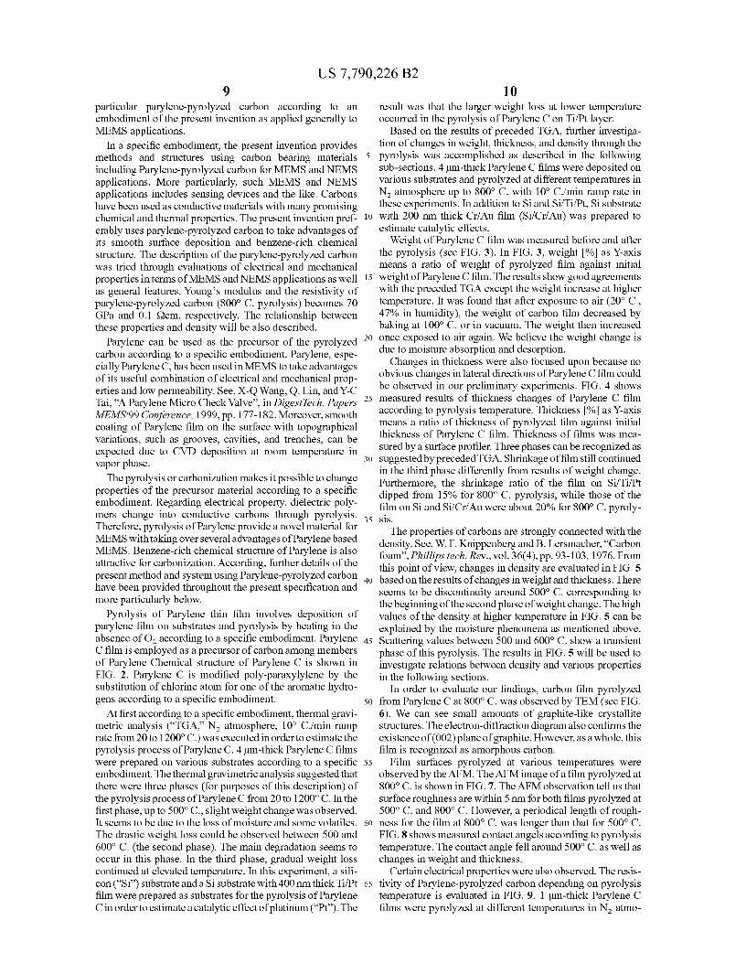
U.S. Patent Sep. 7, 2010 Sheet 2 of 15
US 7,790,226 B2
C1
CH CH2
n
Figure 2: Parylene C chemical structure
100
80
0
s60
buw
40
20
0
♦ Film on Sio Film on Si/Cr/AuX Film on Si/Ti/Pt
0
X
0 200 400 600 800 1000Temperature PAC]
Figure 3: Weight change according pyrolysistemperature (N2, 10°C/min ramp rate)
U.S. Patent Sep. 7, 2010 Sheet 3 of 15 US 7,790,226 B2
100
80
060
ve
40
H
20
0
0
♦ Film on Si0 Film on Si/Cr/AuX Film on Si/Ti/Pt
0
X
0 200 400 600 800 1000
Temperature MI
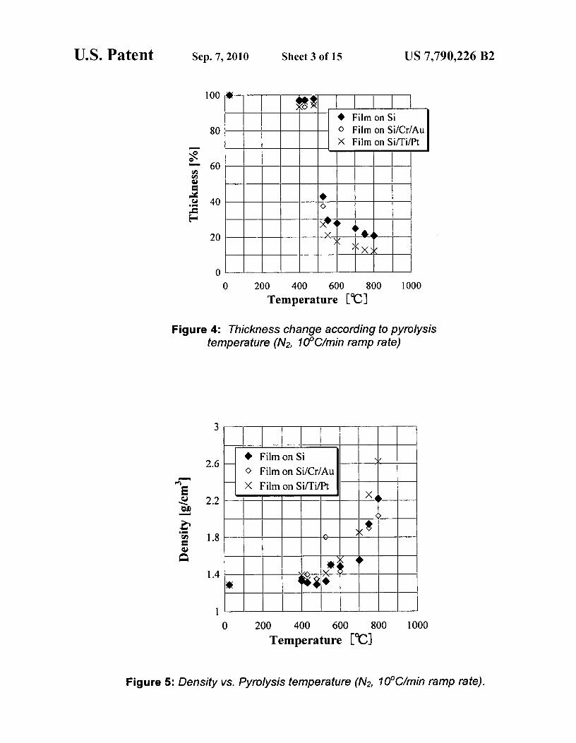
Figure 4: Thickness change according to pyrolysistemperature (N2, 100C/min ramp rate)
♦ Film on Si
0 Film on Si/Cr/AuX Film on Si/Ti/Pt
X
S
♦llE ^♦
0 200 400 600 800 1000
Temperature MI
3
2.6
M
2.2
.Q1.8
asA
1.4
Figure 5: Density vs. Pyrolysis temperature (N2, 100C/min ramp rate).
U.S. Patent Sep. 7, 2010 Sheet 4 of 15 US 7,790,226 B2
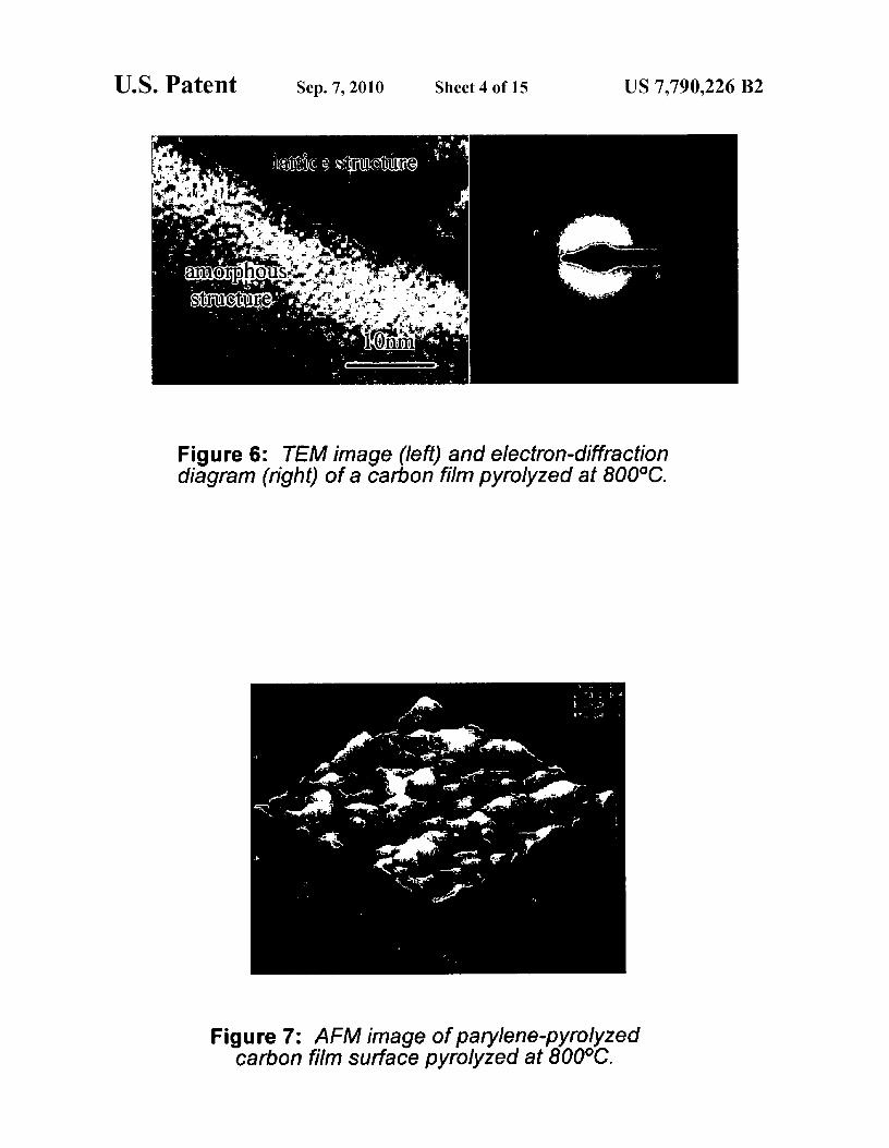
Figure 6: TEM image (left) and electron-diffractiondiagram (right) of a carbon film pyrolyzed at 800°C.
Figure 7: AFM image of parylene-pyrolyzedcarbon film surface pyrolyzed at 800°C.
80
G7WA 70
oA
d 60V
C
U 50
400 200 400 600 800 1000
Temperature M
90
•
• Film on Si
X Film on Si/Cr/Au
A Film on Si/Ti/Pt
U.S. Patent Sep. 7, 2010
Sheet 5 of 15 US 7,790,226 B2
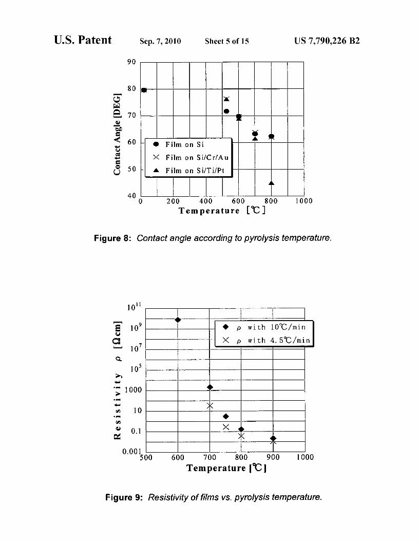
Figure 8: Contact angle according to pyrolysis temperature.
1011
109V
1074
105
1000
10
0.1
0.0015
♦ p with 10°C/min
X p with 4.5 9C /min
X
)0 600 700 800 900 1000
Temperature [9C]
Figure 9: Resistivity of films vs. pyrolysis temperature.
cn
108 4
b
x
1011
waw
10100
a0
109
109
1070 200 400 600 800 1000
Temperature PC]
U.S. Patent Sep. 7, 2010 Sheet 6 of 15 US 7,790,226 B2
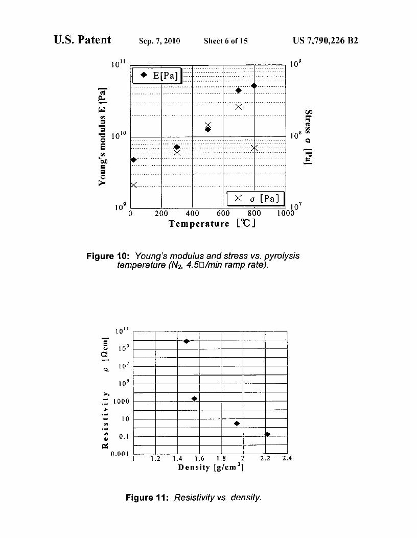
Figure 10: Young's modulus and stress vs. pyrolysistemperature (N2, 4.501min ramp rate).
10"
109cQ 107
105
1000
.r10
.r0.1
a0 001
1 1.2 1.4 1.6 1.8 2 2.2 2.4Density [g/cm31
Figure 11: Resistivity vs. density.

U.S. Patent Sep. 7, 2010 Sheet 7 of 15 US 7,790,226 B2
10 11
.................
...................................
..........................I ...............................................
..............
.............
-........................
.... "... -* 1".
----- I ......
-- -- ---
.......
. ..........
............
--- .......
.......................
......
............
.....................................
..................................................
. - ..... i ... ***'* ...
............
* .... *'*"*'"'*"*
.... ... I ...
.....
..... ......
...... ", ...
. I ..........
........................- ....... :1............
I ..............
..........
.... ....................
.... * .............................-.1 ... I ....
........ ...
..
......
....
....
... ........
............
------------
..
............
............---
* -----------------..................................
........ ...
............
........ I ..
------------........................
........
----.... ......
...... I . ...
............
............
... ........
............
. I ..........
............
. I ..........
1.2 1.4 1.6 1.8 2 2.2 2.4
Density [g/ern 31
Figure 12: Young's modulus vs. density.
IF
1010
109
J
Figure 13: Diagram of possible electrode layout
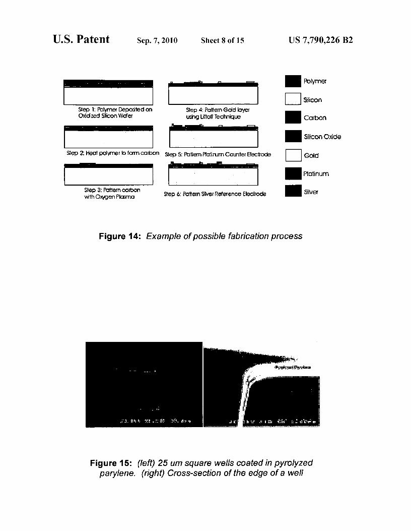
Step I Pattern ocibon%ith Oxygen Plama Step 6: Pattern S'lver Reference Electrode
U.S. Patent Sep. 7, 2010 Sheet 8 of 15
US 7,790,226 B2
OPblyma
Silicon
n Carbon
. Silicon Oxide
FI Gold
n Ptotnum
&Ivef
Sep l: Pblymer Deposited on
Step 4: Pattern Gold layerO)ddzed Shcon Wafer using L'a`toff Technique-
Step Z Heat pdyrner io formearbon Step S: Poem Pfau rum Counter Electrode
Figure 14: Example of possible fabrication process
Figure 15: (left) 25 um square wells coated in pyrolyzedparylene. (right) Cross-section of the edge of a well
iam
icca
MASS
aCU
ffi rnca
i[6!
SAM
ICU
:7CM
ICM
ICUIca
1
U.S. Patent
Sep. 7, 2010
Sheet 9 of 15
US 7,790,226 B2
r^^aa
7I.
•i
oa
.- a37 Ica Bea 'tee 1Q! Boa ^asaerieo
raclz^o
Tirimf?t^rur* ^'C^.^,
Figure 16: Simultaneous thermal analysis data for parylene C(heating rate = 5 1C/min, in flowing Ar at 100mUmin)
-Lacci Mm T'c; .1,550
W:xnia S1M'jC=')
Figure 17: MicroRaman data for parylene C carbonized in furnaceat 1550C (top --- heating rate = 5 1C/min, held at temperature for 5minutes, flowing A @ 100mL/min) and parylene C carbonized onSi (heating rate = 100C/min, held at 900°C for 1 hour, flowing N2 at100 mL/min) showing clearglassy carbon ;eaks, labeled D1 andG, according to (1, 21
R
Eaa^c^ Rx.4aaa^ ^isCt^ePP`) ^caaa^t sensor
R verb TCR a andCw= -- ^ J
U.S. Patent Sep. 7, 2010 Sheet 10 of 15
US 7,790,226 B2
ills [t^•Cl!t\`1.0lyaT/aH^Ri^iiir{ ' 1113LiVj i'Ya[IfF^:!! Lsuni'fYar^
cifiiiYP7iiH7i RI I [amn 10 W340
4d .{] +ry Al: . .I Pi R3 [J- 0.1 G. 1i1- .I
^►..rd .^ a Fn ^.
—Tw—rFC
Figure 18: Cyclic voltammograms of hexacyanoferrate inpotassium chloride using platinum and pyrolyzed paryleneelectrodes.
Figure 19: Standard sesistive bolometer structure

r
U.S. Patent Sep. 7, 2010 Sheet 11 of 15 US 7,790,226 B2
2.0
2..4
2.2
.^, 2..0
1 .a
1'' .d
1_.4
EKdER29 0-0030 O_M1 MOM 0-0033 0.0031'
in (e,)
Figure 20: Resistance temperature dependencefor pyrolyzed parylene
10^ lcr` 1a' W id Ian W
Room Temperature Resistivity 0-
Figure 21: TCR vs. resistivity for variouspyrolyzed-parylene films
0.4
0-2
G-0
1-0
I a-8
U.S. Patent Sep. 7, 2010 Sheet 12 of 15 US 7,790,226 B2
0 10, 20 30 40 5D $0
Exposure to air (mien)
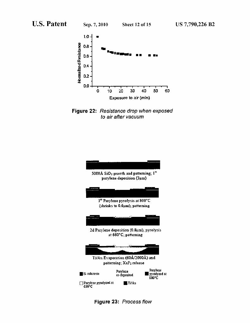
Figure 22: Resistance drop when exposedto air after vacuum
5000.4, SiO 2 growth and pattemang; 1"parylene deposition (3µm)
MWMM^I" Parylene pyrolysis at SOVC(shrinks to 0.6ftm); pattelming
2d Paiylene deposition (O.SFtns), pyrolysisat 660`C; patteming
Ti/Au Evaporation (60 Q-000$) andpatiernine; XeF2 release
Paryleae Parylew
substrate 3s- deposited pyrolyzed atS00°C
Paglene py3oiyzed at Tif.4uOVC
Figure 23: Process flow
U.S. Patent Sep. 7, 2010 Sheet 13 of 15 US 7,790,226 B2
Figure 24: Fabricated bolometer
6. Cal e
S.C%1Cr4
® 4.0 cf,
3.[xie
2.Cxle
1.Crx10J
0.0
0.2 0.4 0.6 0t3 1.0 12 1.6 1.6 13
V(Vclt)
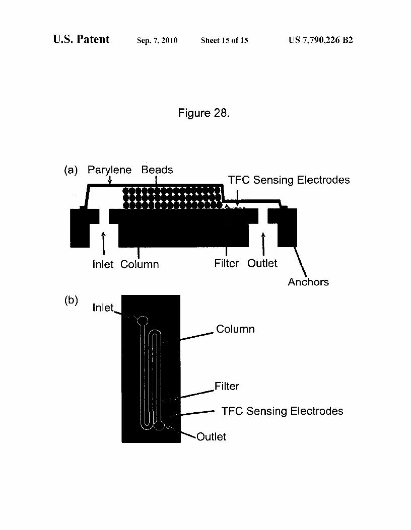
Figure 25: Bolometer IV characteristic
4.Ox10 10 9
3.ax114
N—► 12 $
3.^c1 0 -01
E.
a 3.2x9
IOM C'-
O 2x10'410" 8Xl ' 8x10'* 1x10⁴
1npx, Pcaver (W)
Figure 26: Pixel Resistance and temperature riseas a function of input power

U.S. Patent Sep. 7, 2010
Sheet 14 of 15 US 7,790,226 B2
1: Provide Substrate 4: Pyrotyze Parylene into carbon film
2: Etch Cavity into substrate S: Pattern carbon film
3: Deposit Parylene 6: Etch Substrate around Cavity
FIGURE 27
(a) Parylene BeadsTFC Sensing Electrodes
Column
Filter
TFC Sensing Electrodes
let
(b) Inl
U.S. Patent Sep. 7, 2010 Sheet 15 of 15 US 7,790,226 B2
Figure 28.
Anchors

US 7,790,226 B21
PYROLYZED THIN FILM CARBON
CROSS-REFERENCES TO RELATEDAPPLICATIONS
5
This application claims priority to U.S. Provisional Appli-cation No. 60/538,820 filed Jan. 23, 2004 (Caffech Ref. No.:CIT-403IP) "Pyrolyzed Thin-Film Carbon" which is herebyincorporated by reference in its entirety. This application alsois a continuation-in-part of and claims priority to U.S. appli- 10
cation Ser. No. 10/973,938, now U.S. Pat. No. 7,238,941,filedOct. 25, 2004 (CalTechRef. No.: CIT4032-3974) "Pyro-lyzed-Parylene Based Sensors and Method of Manufacture,"which is hereby incorporated by reference in its entirety, andwhich claims priority to (i) U.S. Provisional Ser. No. 60/538, 15
594 filed Jan. 23, 2004 "Pyrolyzed Parylene UncooledBolometer' ; which is hereby incorporated by reference in itsentirety, and (ii) U.S. Provisional Ser. No. 60/514,627 filedOct. 27, 2003, which is hereby incorporated by reference inits entirety. 20
STATEMENT AS TO RIGHTS TO INVENTIONSMADE UNDER FEDERALLY SPONSORED
RESEARCH OR DEVELOPMENT25
Notice is hereby provided that certain aspects of the inven-tion have been funded, in part, by Center for NeuromorphicSystems Engineering (CNSE) NSF Contract #EEC-9402726and Cell Mimetic Space Exploration (CMISE) NASA GrantNCC2-1364-4. 30
BACKGROUND
The present invention is generally directed to carbon thin 35
films, methods of their deposition, and methods of their use inNanoelectromechanical Systems (NEMS), Microelectrome-chanical Systems (MEMS) and other devices. More particu-larly, the invention provides methods of carbon thin filmdeposition and methods of making carbon containing pat-
40terned structures. The invention also provides methods ofcontrolling physical properties of carbon thin films. More-over, the invention provides methods of use of carbon thinfilms and carbon containing patterned structures in devices.In particular, the invention provides use of carbon thin films 45
as electrochemical sensors in a highperformance liquid chro-matography device.
Electronic systems interface with the real world throughsensors and actuators. The technological development of sen-sors and actuators often relies on the production and charac- 50terization of new materials. MEMS and increasingly NEMSdraw upon traditional semiconductor fabrication methods toproduce novel minituarized sensors and actuators. NEMS andMEMS are often smaller, cheaper and more reliable than theirtraditional counterparts and sometimes open up new possi-
55bilities.
Various forms of carbon are used in many technologicalapplications due to carbon's superior electrical, mechanical,thermal and chemical properties. It is highly desirable toutilize the unique properties of carbon in NEMS and MEMS 60
as well. To introduce carbon into NEMS and MEMS, how-ever, well controlled and well characterized methods of car-bon thin film deposition are desired.
Carbons can be prepared by the pyrolysis of various car-bonaceous precursors such as wood, coal, lignite. Polymers 65
can also be used as precursors of pyrolyzed carbons.Recently, Ranganathan et. al. reported photoresist-derived
2carbon for MEMS and electrochemical applications (see,Ranganathan et al., J. Electrochemical Society, 147 (1), 277-282 (2000)).
Parylene can be an attractive candidate for pyrolysisbecause of its benzene-rich chemical structure. The use ofparylene as the precursor of the pyrolyzed carbon in MEMSprovides a new material for MEMS, while utilizing certainadvantages of parylene based MEMS. Hui et. al. reportedlimited examples of carbon thin films prepared from pyro-lyzed parylene. However, Hui et. al. did not study the detailsof parylene pyrolysis, their method of carbon thin film depo-sition was not optimized, and they did not report the electricaland mechanical properties of their carbon thin films. Conse-quently, the method by Hui et. al. is not characterized enoughand is not controlled enough to be used for introduction ofparylene-pyrolyzed carbon thin films into MEMS or NEMS.
The present invention provides well characterized and wellcontrolled methods of carbon thin film deposition. The inven-tion also provides methods of controlling physical propertiesof carbon thin films. In addition, the present invention pro-vides methods of making carbon containing patterned struc-tures. Further, the present invention provides methods ofusing carbon thin films and carbon containing patternedstructures in NEMS, MEMS and other devices. More particu-larly, the invention provides a method and apparatus for sens-ing electromagnetic radiation in the infrared spectrum using abolometer device. The invention also provides a method andapparatus for sensing chemical species. But it would be rec-ognized that the invention has a much broader range of appli-cability. For example, the invention can be applied to otherwavelengths such as millimeter waves or visible light, bio-logical materials, and other species and/or particles, and thelike.
As technology progresses, certain types of detectiondevices have become important. Detection devices rangefrom motion sensors to those that detect certain frequenciesof electromagnetic radiation and detectors for a variety ofchemical species. Motion sensors include, among others,mechanical, capacitive, inductive, and optical designs. A spe-cific type of motion sensor includes accelerometers and thelike, which rely upon MEMS based technology. Such detec-tion devices also include, among others, infrared detectors,and imagers. An example of an infrared detector is a bolom-eter. Other types of detectors include chemical sensors, whichrely upon sensing differences in voltage potentials whilebeing coupled to an unknown chemical species.
Although many of these sensor designs have had certainsuccess, a variety of drawbacks or limitations still exist. Forexample, conventional bolometer designs are often difficultto manufacture cost efficiently due to constraints in materialsand processing techniques. Additionally, many if not all ofthese sensor designs use conventional mechanical, capaci-tive, inductive, and optical techniques that rely upon a varietyof conventional metals and/or semiconductor materials. Suchmaterials are often limited in the ability to provide an efficientand highly accurate device. Such materials are often reactiveand may degrade over expended periods of time. These andother limitations of conventional devices can be foundthroughout the present specification and more particularlybelow.
From the above, it is seen that an improved technique formanufacturing devices is highly desired.
SUMMARY
The present invention is directed to carbon thin films,devices and articles comprising the carbon thin films, as well
US 7,790,226 B23
4as methods of their deposition and methods of their use in comprise etching the substrate around the cavity. The methodNanoelectromechanical Systems (HEMS), Microelectrome- can further comprise controlling a carbon thin film density bychanical Systems (MEMS), and other devices. More particu- changing the volume of the cavity.larly, the invention provides methods of carbon thin film
Also provided is a method of carbon thin film formation to
deposition and methods of making carbon containing pat- 5 provide good adhesion between the carbon thin film and aterned structures. The invention also provides methods of
substrate comprising: (i) depositing a parylene film on a sub-
controlling physical properties of carbon thin films. More- strate, wherein the substrate does not comprise a prior coatingover, the invention provides methods of use of carbon thin of gamma-methacryloxypropyltrimethoxy silane, alsofilms and carbon containing patterned structures in NEMS, known as Al 74, and (ii) pyrolyzing the parylene film to formMEMS and other devices. io a carbon thin film adhered to the substrate. The substrate can
Many benefits can be achieved by way of the present inven- be silicon, quartz, glass or metal. The step of pyrolyzing thetion over conventional techniques. Existing carbon deposi- parylene film can be performed in the presence of a catalyst.tion techniques (screen printing) generally limit the feature
The catalyst can be a metal. For example, the catalyst can be
size of on-chip electrochemical electrodes to greater than 90
Ti/Pt or Cr/Au. The catalyst can comprise, for example,um and to thicknesses in excess of 5 um with only 12 um 15 nickel, iron, cobalt, platinum, ferrocene, titanium, chrome,resolution in geometric feature definition according to a spe- gold, ferric nitrate, or a combination thereof. The pyrolyzingcific embodiment. The present invention allows for reliable the parylene film can be performed at a temperature rangingand repeatable fabrication of carbon electrodes with feature
from, for example, about 500° C. to about 900° C. The step of
sizes as small as 2 microns, thicknesses as small as 50 mu, and
pyrolyzing the parylene film can be performed in an atmo-geometric resolution as small as 2 microns according to alter- 20 sphere of argon, oxygen, or hydrogen. Alternatively, the pyro-native embodiments. Thin films with even smaller feature
lyzing of the parylene film can be performed in an atmosphere
sizes, thickness, and geometric resolution are achievable. For of nitrogen. The method can further comprise patterning theexample, the feature sizes could be as small as 10 nanometers. carbon thin film. The patterning the carbon thin film can beThis thin-film carbon has the additional benefit of having
done by plasma etching. The parylene film can be a patterned
tunable mechanical and electrical properties. Depending 25 parylene film.upon the embodiment, one or more of these benefits may be
Also provided is a method for forming thin film carbon
achieved. comprising the steps of (i) depositing a hydrocarbon on aIn one specific embodiment, the present invention provides substrate, and (ii) pyrolyzing the hydrocarbon on the sub-
a method of carbon thin film deposition comprising deposit- strate, wherein the pyrolyzing is carried out in the presence ofing a catalyst on a substrate, depositing a hydrocarbon on the so a catalyst which lowers the pyrolysis time and temperature.substrate in contact with the catalyst, and pyrolyzing the
The hydrocarbon can be, for example, parylene. The method
hydrocarbon. The hydrocarbon canbe, for example, parylene. can further comprise patterning the hydrocarbon before pyro-Other examples include polyimide, photoresist, and other
lyzing it, or patterning the pyrolyzed hydrocarbon. The
polymers. The catalyst can be, for example, Ti/Pt or Cr/Au. method can further comprise use of the pyrolyzed hydrocar-The catalyst also can comprise, for example, nickel, iron, 35 bon in HPLC detection.cobalt, platinum, titanium, chrome, gold, ferrocene, or ferric
Still further, the invention provides a use of carbon thin
nitrate. The hydrocarbon can be pyrolyzed at a temperature
films and carbon containing patterned structures in MEMS,ranging from, for example, about 500° C. to about 900° C. NEMS, and other devices. More particularly, the inventionThe pyrolyzing of the hydrocarbon can be performed in an provides a method and apparatus for sensing electromagneticatmosphere of, for example, argon, oxygen, or hydrogen. 4o radiation in the infrared spectrum using a bolometer device.Alternatively, the pyrolyzing of the hydrocarbon can be per- The invention also provides a method and apparatus for sens-formed in an atmosphere of nitrogen. ing chemical species. But it would be recognized that the
In an alternative specific embodiment, the present inven- invention has a much broader range of applicability. Fortionprovides methods of making carbon containing patterned
example, the invention can be applied to other wavelengths
structures. 45 such as millimeterwaves orvisible light, biological materials,One method comprises depositing a hydrocarbon on a sub- and other species and/or particles.
strate, pyrolyzing the hydrocarbon to form a carbon thin film, Ina specific embodiment, the present invention provides anand patterning the carbon thin film by, for example, an etching apparatus for sensing electromagnetic radiation (e.g., bolom-technique. Another method comprises depositing a hydrocar- eter) using carbon based sensing materials, e.g., pyrolyzedbon on a substrate, patterning the hydrocarbon by, for 50 parylene, amorphous carbon based material. The apparatusexample, an etching technique, and pyrolyzing the hydrocar- has a substrate (e.g., silicon, silicon on insulator, other semi-bon. In these methods, the hydrocarbon can be, for example, conductor materials, glass, quartz, metal and organic) com-parylene. The patterning of the carbon thin film or of the prising a surface region and an array of substantially carbonhydrocarbon can be done, for example, by plasma etching. based material regions having a resistivity ranging within aThe patterning can comprise the use of a metal or a photore- 55 predetermined range disposed overlying the surface. In asist mask. The carbon containing patterned structure can have specific embodiment, the predetermined range is from abouta geometric resolution from, for example, about 2 microns to
10$ Ohms cm to about 10 -3 Ohms cm. Each of the carbon
about 10 nanometers. based material regions comprises a portion being suspendedIn yet an alternative specific embodiment, the present over a region of the surface to thermally insulate the portion of
invention provides a method of controlling the physical prop- 60 the suspended carbon based material. In a specific embodi-erties of carbon thin films. More specifically, a carbon thin ment, the insulating region also electrically insulates the por-film density can be controlled by a method comprising etch- tion of the suspended carbon based material. An insulatinging a cavity into a substrate, depositing a hydrocarbon into the region is formed between the region and the portion of thecavity and pyrolyzing the hydrocarbon while in cavity to form carbon based material. Preferably, the insulating region is ana carbon thin film. The hydrocarbon can be, for example, 65 air gap or other like structure according to a specific embodi-parylene. The method can further comprise etching the car- ment. The insulating region can also include multiple regionsbon thin film by plasma etching. The method can further and/or layers, depending upon the embodiment. Each of the
US 7,790,226 B25
carbon based material regions is a pixel element for a pluralityof pixel regions according to a specific embodiment. Theapparatus has an interconnection coupled to each of the car-bon based material regions. Preferably, the interconnection ismade of a pyrolyzed carbon based material and/or metalbased material, e.g., aluminum, copper, gold, silver, titanium,platinum, tungsten, and alloys, and/or any combination ofthese materials, and the like. One or more nodes couples to theinterconnection. Preferably, the one or more nodes is able toindependently read a resistivity value associated with (e.g.,directly connected, coupled) at least one or more of the car-bon based material regions. Preferably, each of the carbonbased regions (or pixel elements) may change in resistivityvalue upon receiving a dosage of electromagnetic radiation,e.g., 8-14 micron wavelength band, 3-5 micron band. Thecarbon based region changes in temperature upon irradiation,which causes a resulting change in resistivity, which can beread out via interconnections and/or related reading devices.
In an alternative specific embodiment, the present inven-tion provides a method for fabricating a sensing device, e.g.,radiation. The method includes providing a substrate com-prising a surface region. The method includes forming aninsulating material overlying the surface region and forminga film of carbon based material overlying the insulating mate-rial. The method includes treating to the film of carbon basedmaterial to pyrolyzed the carbon based material to causeformation of a film of substantially carbon based materialhaving a resistivity ranging within a predetermined range. Ina specific embodiment, the predetermined range is from about10$ Ohms cm to about 10' Ohms cm. Preferably, the methodalso forms a gap underlying a portion of pyrolyzed carbonbased material.
In yet an alternative specific embodiment, the presentinvention provides an apparatus for chemical sensing usingcarbon based sensing materials. The apparatus has a pyro-lyzed parylene carbon based electrode structure having aresistivity ranging within a predetermined range. Preferably,the electrode has a first end coupled to a second end and alength defined between the first end and the second end. Aninterconnect is coupled to at least one of the ends.
Still further, the invention provides a method for fabricat-ing a sensing device. The method includes providing a sub-strate comprising a surface region and forming an insulatingmaterial overlying the surface region. The method alsoincludes forming a film of carbon based material overlyingthe insulating material and treating to the film of carbon basedmaterial to pyrolyzed the carbon based material to causeformation of a film of substantially carbon based materialhaving a resistivity ranging within a predetermined range. Ina specific embodiment, the predetermined range is from about10$ Ohms cm to about 10-3 Ohms cm. The method alsoprovides at least a portion of the pyrolyzed carbon basedmaterial in a sensor application and uses the portion of thepyrolyzed carbon based material in the sensing application. Ina specific embodiment, the sensing application is selectedfrom chemical, humidity, mechanical strain, radiation or ther-mal.
Many benefits are achieved by way of the present inventionover conventional techniques. For example, the present tech-nique provides an easy to use process that relies upon con-ventional technology. In some embodiments, the method pro-vides higher device yields. Additionally, the method providesa process that is compatible with conventional process tech-nology without substantial modifications to conventionalequipment and processes. Preferably, the invention providesfor a method and device that can provide for room tempera-ture detection of certain infrared frequencies according to a
6specific embodiment. Additionally, the present invention pro-vides a sensing material that is generally easy to use, inert,light weight, and has good detection characteristics, e.g.,signal to noise ratio. Using Parylene, which has been pyro-
5 lyzed, rather than conventional materials allows for improve-ments in performance due to its mechanical and thermalproperties. As for the chemical sensor, there does not pres-ently exist any other method for constructing a continuouselectrode over insulating high aspect ratio micromachined
io structures according to an embodiment of the present inven-tion. This property of pyrolyzed parylene makes three dimen-sional micromachined electrodes possible. Depending uponthe embodiment, one or more of these benefits may beachieved. These and other benefits will be described in more
15 throughout the present specification and more particularlybelow.
Various additional objects, features and advantages of thepresent invention can be more fully appreciated with refer-ence to the detailed description and accompanying drawings
20 that follow.
BRIEF DESCRIPTION OF THE DRAWINGS
FIG. 1 is a simplified process flow diagram illustrating a25 fabrication sequence for a sensing device according to an
embodiment of the present invention;FIG. 2 is a simplified diagram of parylene C chemical
structure according to an embodiment of the present inven-tion;
30 FIG. 3-12 are simplified diagrams illustrating characteris-tics of parylene pyrolysis according to embodiments of thepresent invention;
FIG. 13 is a simplified diagram of a chemical sensingdevice according to an embodiment of the present invention;
35 FIG. 14 is a simplified diagram illustrating a fabricationsequence for a chemical sensing device according to anembodiment of the present invention;
FIGS. 15 through 18 are simplified diagrams illustrateexperimental results of a chemical sensing device according
40 to an embodiment of the present invention;FIG. 19 is a simplified diagram of a bolometer device
according to an embodiment of the present invention;FIGS. 20 -22 are simplified diagrams illustrating experi-
mental results of a bolometer device according to an embodi-45 ment of the present invention;
FIG. 23 is a simplified diagram illustrating a fabricationsequence for a bolometer device according to an embodimentof the present invention;
FIG. 24 is a simplified top-view illustration of a bolometerso device according to an embodiment of the present invention;
andFIGS. 25-26 are simplified diagrams illustrating bolometer
characteristics according to embodiments of the present
55 invention
FIG. 27 illustrates a method of controlling carbon thin filmdensity.
FIG. 28 illustrates a carbon thin film based electrochemicalsensor incorporated into a High Performance Liquid Chro-
60 matography column.
DETAILED DESCRIPTION OF THE INVENTION
The following two references are hereby incorporated by65 reference in their entirety:
Matthieu Liger, Satoshi Konishi and Yu-Chong Tai,"UncooledAll-Parylene Bolometer", The 17th IEEE Interna-
US 7,790,226 B27
tional MEMS Conference (MEMS'04), Maastricht, Nether-lands Jan. 15-29, 2004, p 593-596.
Satoshi Konishi, Matthieu Liger, Theodore Harder, andYu-Chong Tai, "Parylene-Pyrolyzed Carbon for MEMSApplications", The 17th IEEE International MEMS Confer-ence (MEMS'04), Maastricht, Netherlands Jan. 15-29, 2004,p 161-164.
The present invention is directed to carbon thin films,methods of their deposition and methods of their use in Nano-electromechanical Systems (NEMS), Microelectromechani-cal Systems (MEMS), and other devices. More particularly,the invention provides methods of carbon thin film depositionand methods of making carbon containing patterned struc-tures. The invention also provides methods of controllingphysical properties of carbon thin films. Moreover, the inven-tion provides methods of use of carbon thin films and carboncontaining patterned structures in NEMS, MEMS and otherdevices.
In one specific embodiment, the present invention providesa method of carbon thin film deposition comprising deposit-ing a catalyst on a substrate, depositing a hydrocarbon on thesubstrate in contact with the catalyst, and pyrolyzing thehydrocarbon. For this embodiment, the substrate can be sili-con or other semiconductor material, glass, quartz, metal ororganic material, and the hydrocarbon can be parylene,PDMS, polyethylene, Teflon, orbenzene; but most preferablyparylene. The catalyst can be Ti/Pt or Cr/Au. The catalyst canalso comprise at least one selected from the group consistingof nickel, iron, cobalt, platinum, ferrocene, titanium, chrome,gold, or ferric nitrate. Pyrolyzing the hydrocarbon can beperformed in an atmosphere of nitrogen, argon, oxygen orhydrogen. In the most preferred embodiment, pyrolyzing thehydrocarbon is performed in the presence of a nitrogen atmo-sphere. Most preferably, pyrolyzing the hydrocarbon is per-formed in the temperature range from about 500° C. up toabout 900° C. Pyrolyzing the hydrocarbon is achieved byraising the temperature of the hydrocarbon to a temperaturewhere it decomposes and holding it there a specific amount oftime to produce a carbon thin film.
In an alternative specific embodiment, the present inven-tionprovides methods of making carbon containing patternedstructures. One method comprises depositing a hydrocarbonon a substrate, pyrolyzing the hydrocarbon to form a carbonthin film, and patterning the carbon thin film by an etchingtechnique. The other method comprises depositing a hydro-carbon on a substrate, patterning the hydrocarbon by an etch-ing technique, and pyrolyzing the hydrocarbon. The etchingtechnique to be used for patterning the carbon thin film or forpatterning the hydrocarbon can be plasma etching, chemicaletching or physical removal.
In yet an alternative specific embodiment, the presentinvention provides a method of controlling physical proper-ties of carbon thin films. More specifically, a carbon thin filmdensity is controlled by a method comprising etching a cavityinto a substrate, depositing a hydrocarbon into the cavity andpyrolyzing the hydrocarbon while in cavity to form a carbonthin film (see, for example, FIG. 27). Controlling the carbonthin film density can be achieved by changing the volume ofthe cavity. The method of controlling the physical propertiesof carbon thin films can further comprise etching the carbonthin film or alternatively etching the substrate around thecavity.
The illustration shown in FIG. 27 provides a method com-prising at least some of the following steps:
(a) providing a substrate; the substrate can be flat.(b) etching a cavity into the substrate; the cavity can be, for
example, a channel.
8(c) depositing a hydrocarbon such as, for example,
parylene, into the cavity; the hydrocarbon can be also depos-ited on the substrate surface away from the cavity.
(d) pyrolyzing the hydrocarbon, such as parylene, in the5 cavity, to form carbon in the cavity; pyrolysis of the hydro-
carbon can also occur on the substrate surface away from thecavity.
(e)patterning the carbon film; this can remove carbon awayfrom the cavity.
to (f) etching substrate around the cavity; this can yield ananoscopic or microscopic piece of carbon disposed on asubstrate.
In yet another specific embodiment, the present inventionprovides methods of using carbon thin films to produce
15 MEMS or NEMS and other useful devices and structures.According to the present invention, techniques directed to
sensing devices and their processing are provided. More par-ticularly, the invention provides a method and apparatus forsensing electromagnetic radiation in the infrared spectrum
20 using a bolometer device. The invention also provides amethod and apparatus for sensing chemical species. But itwould be recognized that the invention has a much broaderrange of applicability. For example, the invention can beapplied to other wavelengths such as millimeter waves or
25 visible light, biological materials, and other species and/orparticles.
A method according to an embodiment of the presentinvention for fabricating a sensing device is briefly outlinedbelow, which can also be referenced in the simplified flow
3o diagram 100 of FIG. 1. At least some of the following stepscan be carried out:1. Start process (step 101);2. Provide a substrate (e.g., silicon, glass, organic, metal)
(step 103) comprising a surface region;35 3. Clean (step 105) the surface region;
4. Form (step 107) an insulating material (e.g., silicon nitride,silicon oxide) overlying the surface region;
5. Form (step 109) a film of carbon based material or hydro-
40carbon (e.g., Parylene) overlying the insulating material;
6. Treat (step 111) the film of carbon based material or hydro-carbon (e.g., parylene) to pyrolyze the carbon based mate-rial or hydrocarbon;
7. Cause (step 113) formation of a film of substantially carbon45 based material having a resistivity ranging within a prede-
termined range based upon at least the treatment;8.Provide (step 115) at least a portion of the pyrolyzed carbon
based material in a sensing application;9. Use (step 117) the portion of the pyrolyzed carbon based
50 material in the sensing application;10. Detect (step 119) a change in characteristic (e.g., resis-
tance) of the pyrolyzed carbon based material from anapplication of electromagnetic radiation and/or chemicaland/or biological species and/or other entities; and
55 11. Perform (step 121) other steps, as desired.The above sequence of steps provides a method according
to an embodiment of the present invention. As shown, themethod uses a combination of steps including a way of form-ing a sensing device using a pyrolyzed parylene bearing mate-
6o rial or the like. Other alternatives can also be provided wheresteps are added, one or more steps are removed, or one ormore steps are provided in a different sequence withoutdeparting from the scope of the claims herein. Further detailsof the present method and structure can be found throughout
65 the present specification and more particularly below. Beforediscussing specific sensor type applications, we have pro-vided a brief description of a carbon based material and in
US 7,790,226 B29
10particular parylene-pyrolyzed carbon according to anembodiment of the present invention as applied generally toMEMS applications.
In a specific embodiment, the present invention providesmethods and structures using carbon bearing materialsincluding Parylene-pyrolyzed carbon for MEMS and NEMSapplications. More particularly, such MEMS and NEMSapplications includes sensing devices and the like. Carbonshave been used as conductive materials with many promisingchemical and thermal properties. The present invention pref-erably uses parylene-pyrolyzed carbon to take advantages ofits smooth surface deposition and benzene-rich chemicalstructure. The description of the parylene-pyrolyzed carbonwas tried through evaluations of electrical and mechanicalproperties in terms of MEMS and NEMS applications as wellas general features. Young's modulus and the resistivity ofparylene-pyrolyzed carbon (800° C. pyrolysis) becomes 70GPa and 0.1 Qcm, respectively. The relationship betweenthese properties and density will be also described.
Parylene can be used as the precursor of the pyrolyzedcarbon according to a specific embodiment. Parylene, espe-cially Parylene C, has been used in MEMS to take advantagesof its useful combination of electrical and mechanical prop-erties and low permeability. See, X-Q Wang, Q. Lin, andY-CTai, A Parylene Micro Check Valve", in DigestTech. PapersMEMS199 Conference, 1999, pp. 177-182. Moreover, smoothcoating of Parylene film on the surface with topographicalvariations, such as grooves, cavities, and trenches, can beexpected due to CVD deposition at room temperature invapor phase.
The pyrolysis or carbonization makes it possible to changeproperties of the precursor material according to a specificembodiment. Regarding electrical property, dielectric poly-mers change into conductive carbons through pyrolysis.Therefore, pyrolysis of Parylene provide a novel material forMEMS withtaking over several advantages of Parylene basedMEMS. Benzene-rich chemical structure of Parylene is alsoattractive for carbonization. According, further details of thepresent method and system using Parylene-pyrolyzed carbonhave been provided throughout the present specification andmore particularly below.
Pyrolysis of Parylene thin film involves deposition ofparylene film on substrates and pyrolysis by heating in theabsence of Oz according to a specific embodiment. ParyleneC film is employed as a precursor of carbon among membersof Parylene Chemical structure of Parylene C is shown inFIG. 2. Parylene C is modified poly-paraxylylene by thesubstitution of chlorine atom for one of the aromatic hydro-gens according to a specific embodiment.
At first according to a specific embodiment, thermal gravi-metric analysis ("TGA," N 2 atmosphere, 10° C./min ramprate from 20 to 1200° C.) was executed in order to estimate thepyrolysis process of Parylene C. 4 µm-thick Parylene C filmswere prepared on various substrates according to a specificembodiment. Thethermal gravimetric analysis suggestedthatthere were three phases (for purposes of this description) ofthe pyrolysis process of Parylene C from 20 to 1200° C. In thefirst phase, up to 500° C., slight weight change was observed.It seems to be due to the loss of moisture and some volatiles.The drastic weight loss could be observed between 500 and600° C. (the second phase). The main degradation seems tooccur in this phase. In the third phase, gradual weight losscontinued at elevated temperature. In this experiment, a sili-con ("Si") substrate and a Si substrate with 400 mu thick Ti/Ptfilm were prepared as substrates for the pyrolysis of ParyleneC in order to estimate a catalytic effect of platinum ("Pt"). The
result was that the larger weight loss at lower temperatureoccurred in the pyrolysis of Parylene C on Ti/Pt layer.
Based on the results of preceded TGA, further investiga-tion of changes in weight, thickness, and density through the
5 pyrolysis was accomplished as described in the followingsub-sections. 4 µm-thick Parylene C films were deposited onvarious substrates and pyrolyzed at different temperatures inNz atmosphere up to 800° C. with 10° C./min ramp rate inthese experiments. In addition to Si and Si/Ti/Pt, Si substrate
io with 200 nm thick Cr/Au film (Si/Cr/Au) was prepared toestimate catalytic effects.
Weight of Parylene C film was measured before and afterthe pyrolysis (see FIG. 3). In FIG. 3, weight [%] as Y-axismeans a ratio of weight of pyrolyzed film against initial
15 weight of Parylene C film. The results show good agreementswith the preceded TGA except the weight increase at highertemperature. It was found that after exposure to air (20° C.,47% in humidity), the weight of carbon film decreased bybaking at 100° C. or in vacuum. The weight then increased
20 once exposed to air again. We believe the weight change isdue to moisture absorption and desorption.
Changes in thickness were also focused upon because noobvious changes in lateral directions of Parylene C film couldbe observed in our preliminary experiments. FIG. 4 shows
25 measured results of thickness changes of Parylene C filmaccording to pyrolysis temperature. Thickness [%] as Y-axismeans a ratio of thickness of pyrolyzed film against initialthickness of Parylene C film. Thickness of films was mea-sured bya surface profiler. Three phases can be recognized as
30 suggested by preceded TGA. Shrinkage of film still continuedin the third phase differently from results of weight change.Furthermore, the shrinkage ratio of the film on Si/Ti/Ptdipped from 15% for 800° C. pyrolysis, while those of thefilm on Si and Si/Cr/Au were about 20% for 800° C. pyroly-
35 sis.The properties of carbons are strongly connected with the
density. See, W. F. Knippenberg and B. Lersmacher, "Carbonfoam", Phillips tech. Rev., vol. 36(4), pp. 93-103,1976. Fromthis point of view, changes in density are evaluated in FIG. 5
4o based on theresults of changes in weight and thickness. Thereseems to be discontinuity around 500° C. corresponding tothe beginning of the second phase of weight change. The highvalues of the density at higher temperature in FIG. 5 can beexplained by the moisture phenomena as mentioned above.
45 Scattering values between 500 and 600° C. show a transientphase of this pyrolysis. The results in FIG. 5 will be used toinvestigate relations between density and various propertiesin the following sections.
In order to evaluate our findings, carbon film pyrolyzed50 from Parylene C at 800° C. was observed by TEM (see FIG.
6). We can see small amounts of graphite-like crystallitestructures. The electron-diffraction diagram also confirms theexistence of (002) plane of graphite. However, as a whole, thisfilm is recognized as amorphous carbon.
55 Film surfaces pyrolyzed at various temperatures wereobserved by the AFM. The AFM image of a film pyrolyzed at800° C. is shown in FIG. 7. The AFM observation tell us thatsurface roughness are within 5 nm for both films pyrolyzed at500° C. and 800° C. However, a periodical length of rough-
6o ness for the film at 800° C. was longer than that for 500° C.FIG. 8 shows measured contact angels according to pyrolysistemperature. The contact angle fell around 500° C. as well aschanges in weight and thickness.
Certain electrical properties were also observed. Theresis-65 tivity of Parylene-pyrolyzed carbon depending on pyrolysis
temperature is evaluated in FIG. 9. 1 µm-thick Parylene Cfilms were pyrolyzed at different temperatures in N 2 atmo-
US 7,790,226 B211
12sphere up to 900. The resistivity was calculated from mea-sured sheet resistance and film thickness. The ramp rate ofelevated temperature were set at two values (10° C./min and4.5° C./min) and compared in this experiment.
Parylene C films pyrolyzed at a low pyrolysis temperatureexhibited high resistivity. The resistivity became less than1x10 10 Qcm above 600° C. and decreased to about 1x10 -2
Qcm at 900'C., which was clo se to 5x 10⁻³ Qcm reported forglassy carbons obtained above 1000° C. See, S. Ranganathan,R. McCreery, S. M. Majji, and M. Madou, "Photoresist-de-rived for microelectromechanical Systems and Electrochemi-cal applications", Journal of The Electrochemical Society,147(1), pp. 277-282, 2000. The pyrolysis with a lower ramprate could provide a lower resistivity.
Next, the Young's modulus and the stress of Parylene-pyrolyzed carbon were evaluated by the diaphragm load-deflection tests. The deformation of the carbon diaphragmpyrolyzed from 3 µm-thick Parylene C on Si frame structurewas measured according to supplied pressure. See, O. Tabata,K. Kawahata, S. Sugiyama, and I. Igarashi, "Mechanicalproperty measurements of thin-films using load deflection ofcomposite rectangular membranes", Sensors and Actuators,vol. 20, pp. 135-141, 1989. Both Young's modulus and thestress are simultaneously obtainedby fitting the resulting datato the load-deflection relationship reported by O. Tabata, K.Kawahata, S. Sugiyama, and I. Igarashi, "Mechanical prop-erty measurements of thin-films using load deflection of com-posite rectangular membranes", Sensors and Actuators, vol.20, pp. 135-141, 1989.3 µm-thick Parylene C membranes onSi frame structures as specimens were prepared as follows. 3µm-thick Parylene C film was deposited on a 20 µm-thick Sidiaphragm structure and released to form Parylene C mem-brane by BrF 3 etching of remaining 20 µm-thick Si layer.
FIG. 10 shows calculated Young's modulus and the stressaccording to pyrolysis temperature. In the calculation, a Pois-son's ratio was assumed to be 0.4. TheYoung's modulus afterthe pyrolysis became —50 GPa for 800° C. pyrolysis (4.5°C./min ramp rate). The stress also increased below 700° C.but showed a drop at 800° C.
Considerable evidences was seen to prove catalytic effectsof Pt for pyrolysis of Parylene C in most of presented results.These results are presumable because Pt shows catalyticeffects in many other chemical reactions while further inves-tigation into our case is necessary.
Next, relations between properties and density ofparylene-pyrolyzed carbon are discussed. Here, density is calculatedby using weight of film in air, that is to say, weight withmoisture. Therelationship between the Young's modulus andthe density is shown in FIG. 12. FIG. 12 tells that a largerdensity corresponds to a larger Young's modulus. Moreover,the relationship between the resistivity and the density is alsodepicted in FIG. 11 that a higher density corresponds to alower resistivity.
As noted above, Parylene-pyrolyzed carbon for MEMSapplications has been provided. Young's modulus and resis-tivity of parylene-pyrolyzed carbon (800° C. pyrolysis)showed 70 GPa and 0.1 Qcm, respectively. The relationsbetween these properties and density were also discussed.Further details of the use of Parylene-pyrolyzed carbon forsensing devices according to embodiments of the presentinvention can be found throughout the present specificationand more particularly below.
Electrochemical SensorElectrochemical sensors can be used in a wide variety of
applications including pH monitoring, gas monitoring, andion detection. Electrochemical sensors are also used as abasic
laboratory instrument to study the chemical behavior andkinetics of many reactive species. Electrochemical sensorsexperience enhanced performance when they have micronand submicron feature sizes and are composed of highly inert
5 materials. This sensor combines both micron feature sizeswith a novel inert thin-film carbon that is compatible withstandard surface micromachining processes. The ability todeposit a thin-film carbon and pattern it using photolithogra-phy improves device performance and simplifies device
io manufacturing compared to screen printed carbon which isthe only other available method for on-chip carbon elec-trodes.
FIG. 13 shows an example of the concept of the thin-filmcarbon electrochemical sensor 1300 according to a specific
15 embodiment. This diagram is merely an example, whichshould not unduly limit the scope of the claims herein. One ofordinary skill in the art would recognize other variations,modifications, and alternatives. As shown, various electrodeelements 1305, 1303, 1309 can be disposed on an insulating
20 material 1301. The insulating material can be, for example,silicon dioxide or other film or films of insulating character-istics. The electrodes can include reference electrode 1303and electrode 1309, which can be made respectively of, forexample, platinum and silver. Each of these electrodes can
25 include conductive wiring 1307, which is coupled to a mea-suring device. Preferably, the sensor also can include carbonbased electrode 1305 formed on the insulating material. Ofcourse, there can be other variations, modifications, and alter-natives.
30 In a specific embodiment, the carbon layer is constructedby first depositing a hydrocarbon or a carbon containingpolymer. Such polymers include but are not limited to allvarieties of photoresist, Parylene N, Parylene C, and ParyleneD. Photoresist can be spun on, while all three types of
35 Parylene can be deposited by vapor deposition. The polymeris then heated to temperatures in excess of 450° C. in an inertatmosphere to force the polymer to undergo pyrolysis accord-ing to a specific embodiment. By varying the pyrolysis tem-perature several material properties can be controlled such as
40 the carbon's porosity, resistivity, density, thickness, thermalconductivity, grain structure, and other parameters. Theresulting layer of carbon can then be patterned using standardphotolithographic and plasma etching techniques. Variationson this process include (i) the addition of a metal catalyzer
45 (e.g., nickel, gold, platinum, titanium) above or below thepolymer, and (ii) modification of the carbon's surface withion selective membranes or other specialized polymers suchas, e.g., Nation. Additional metallization layers can be addedto the carbon to construct counter and reference electrodes as
50 well as on-chip wiring and bonding pads. These metallizationlayers can be patterned through standard metal lift-off tech-niques. Such metallization layers include, for example, alu-minum, gold, platinum, copper, silver, and others. As noted,the chip can then be wired to an external potentiostat to
55 conduct a wide variety of electrochemical studies. Of course,there can be other variations, modifications, and alternatives.Details of a way of processing the carbon based electrode canbe found throughout the present specification and more par-ticularly below.
60 FIG. 14 is a simplified diagram illustrating a fabricationsequence for a chemical sensing device according to anembodiment of the present invention. This diagram is merelyan example, which should not unduly limit the scope of theclaims herein. One of ordinary skill in the art would recognize
65 many variations, modifications, and alternatives. As shown,the process starts (step 1) with the oxidation of a silicon waferor the use of a high-temperature quartz wafer or other suitable

US 7,790,226 B213
materials including inorganic materials. Alternatively, othertypes of substrates (e.g., organic) can be used. Additionally,other types of insulating films can also be used. The carboncontaining polymer can be deposited either by spinning it onthe wafer or by vapor deposition according to a specificembodiment. If a metal catalysis is being used, it can bedeposited and patterned by thermal evaporation, sputtering,or e-beam evaporation prior to the deposition of the polymer.An example of such metal catalyzer is nickel, but it can beothers.
Referring to step 2, the wafer with the polymer is thenheated to the desired pyrolysis temperature in an inert (e.g.,argon or nitrogen) atmosphere or vacuum. After pyrolysis thecarbon layer is patterned (step 3) using O z plasma etchingwith a photoresist mask. The wafer is then prepared for metalliftoff by depositing and patterning a layer of photoresist.Alternatively, other types of etching techniques can be useddepending upon the embodiment.
A gold metal layer is deposited (step 4) to form wires andbonding pads. Alternatively, other types of metals such asaluminum, platinum, and silver can also be used. Two addi-tional metal layers of platinum and silver are deposited andpatterned (steps 5 and 6) in the same manner to form thecounter and reference electrodes, respectfully. These addi-tional layers are optional depending on the application. Anadditional layer of Parylene is also optional. This additionallayer, for example, can serve as a chemical barrier to isolateon-chip wires and to better control the geometry of theexposed electrode surface. This layer can be patterned usingan Oz plasma etching with a photoresist mask. Of course,there can be other variations, modifications, and alternatives.
Existing carbon deposition techniques (screen printing)limit the feature size of on-chip electrochemical electrodes togreater than 90 um and to thicknesses in excess of 5 um withonly 12 um resolution in geometric feature definition accord-ing to a specific embodiment. This present carbon depositiontechnology allows for reliable and repeatable fabrication ofcarbon electrodes with feature sizes as small as 2 um, thick-nesses as small as 50 mu, and geometric resolution as small as2 microns, or even as small as 1 micron, 500 mu, or 10 mu,according to alternative embodiments. This thin-film carbonhas the additional benefit of having tunable mechanical andelectrical properties. Depending upon the embodiment, oneor more of these benefits may be achieved.
Although the above has been described in terms of specificembodiments, there are other variations, modifications, andalternatives. As merely an example, certain device geometrycan be varied from application to application according to aspecific embodiment. For example, such device geometry canbe inter-digitated electrodes, micromachined posts, andchanges in electrode length and width. Alternatively, metalsused as counter and reference electrodes and for bonding padsand wiring can be varied (e.g., shorting reference and counterelectrodes or using an electrode as a preconcentrator (elec-trochemical stripping) according to other embodiments. Dif-ferent carbon polymers may be used as the carbon sourceaccording to a specific embodiment. Such carbon polymerscan include, among others, photoresist and other types ofparylene. A metal catalysis (e.g., nickel or gold) may be usedto further tune the carbon layer's mechanical and electricalproperties in other embodiments. A variety of ion selectivemembranes (e.g., Nation) may be used to coat the carbonelectrode to increase electrochemical sensitivity and selectiv-ity for particular analytes in yet other embodiments. Forexample, such coatings can include Nation or polypyrrole.Mechanical structures can be added near the electrodes to aidin fluid containment and transport in further embodiments.
14For example, such structures can be micro-fluidic channels. Acoating or other type of insulation (e.g., Parylene) may beadded to isolate parts of the chip from the chemical solution inalternative embodiments. Depending upon the embodiment,
5 there can be other variations, alternatives, and modifications.
HPLC EmbodimentIn a specific embodiment, the thin film of carbon can serve
as an electrochemical sensor in a liquid chromatographicto device, including an HPLC device. The micromachining fab-
rication process used to make the present invention also canbe used to fabricate an HPLC device. HPLC devices, andmethods of making and using them, are described, forexample, in the following US patent applications: (1) "Design
15 of an IC-Processed Polymer Nano-Liquid ChromatographySystems On-a-Chip and Method of Making It" Ser. No.10/917,257, filed on Aug. 11, 2004 (CalTech Ref. No.: CIT-3936); (2) "On-Chip Temperature Controlled Liquid Chro-matography Methods and Devices" Ser. No. 60/545,727, filed
20 on Feb. 17, 2004 (Caffech Ref. No.: CIT-4046P), both ofwhich are hereby incorporated by reference in their entirety.
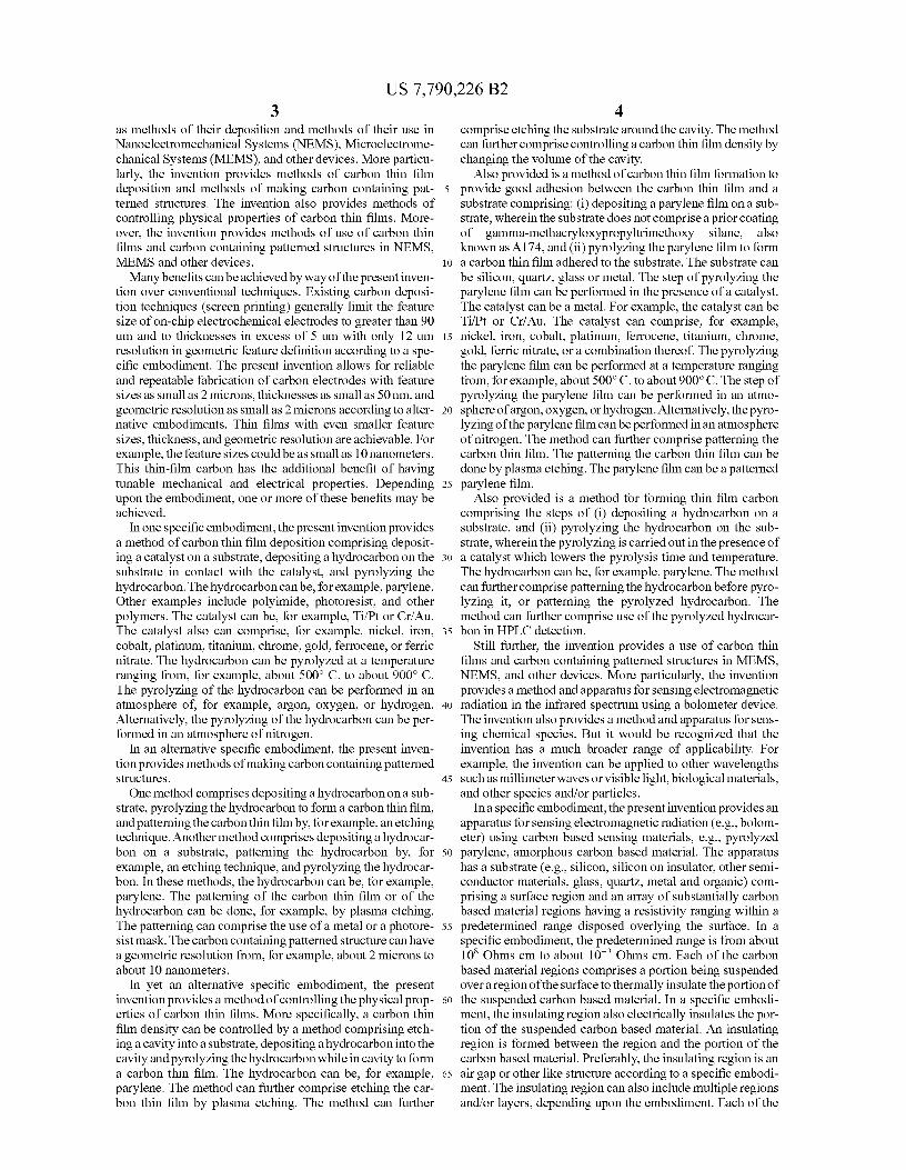
FIGS. 28(a) and (b) illustrates an example of an HPLCdevice. FIG. 28(a) illustrates a side view of the device com-prising an inlet, a parylene layer defining a chromatographic
25 media comprising, for example, beads, a filter, one more ofthin film carbon (TFC) sensing electrodes, anchors, and anoutlet. FIG. 28(b) illustrates a top view, showing the inlet, thecolumn, the filter, the TFC sensing electrodes, and the outlet.
30 WORKING EXAMPLES
The inventions are further described with use of the fol-lowing working examples. To prove the principle and opera-tion of the chemical sensor technique in the present invention,
35 experiments were performed. These experiments are merelyexamples and should not unduly limit the scope of the claimsherein. One of ordinary skill in the art would recognize manyvariations, modifications, and alternatives. In these experi-ments, thin-film carbon microelectrodes were fabricated for
40 integration into a variety of chemical and biochemical sen-sors. The carbon films were compatible with standard MEMSprocessing, most importantly photolithography, and stillmaintained many if not all the electrochemical benefits ofcarbon. Pyrolyzed parylene-C not only meets these desired
45 requirements, but it is also conformal over high aspect ratiostructures. Conformal carbon coating could be used to makehigh effective surface area electrodes by coating high aspectratio structures (See, for example, FIG. 15).
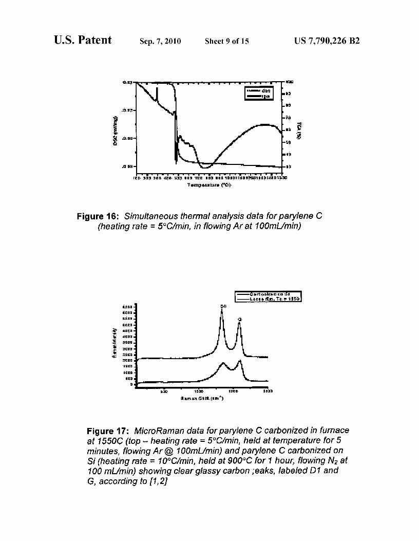
A free standing film of parylene-C (15.8 mg) was exam-50 ined by simultaneous thermal analysis, which provides
thereto gravimetric analysis and differential scanning calo-rimetry. The sample was heated to 1500 Degrees Celsius witha heating rate of 5 Degrees Celsius/min in flowing Ar (100mL/min). As seen in FIG. 16, the material undergoes an
55 endothermic phase transition, presumably melting, at 296Degrees Celsius. An exothermic event peaks near 480Degrees Celsius, and is accompanied by a weight loss of 66%.Total weight loss to 1500 Degrees Celsius is 70.1%.
Micro Raman analysis was conducted on both loose film6o and attached parylene samples (FIG. 17). Parylene carbon-
ized at 900 Degrees Celsius on Si shows broad and poorlydefined G and DI peaks, whereas carbonization at 1550Degrees Celsius in flowing Ar resulted in narrow and well-defined peaks, clearly indicative of glassy carbon. The band
65 near 1580 cm-1 is known as the graphite band (G band) andcorresponds to the in-plane vibration of C atoms in graphitestructure [See O. Beyssac, B. Goffe, et. al, "On the charac-
US 7,790,226 B215
terization of disordered and heterogeneous carbonaceousmaterials by Raman spectroscopy," SpectrochimicaActa PartA, 59 2267-76 (2003); also F. Tuinstra and J. L. Koenig,"Raman spectrum of graphite," J. Chem. Phys., 53 [3] 1126-30 (1970)] For perfect single crystal graphite, it would be theonly band observed. The presence of the so-called defect band(Dl) around 1350 cm-1 indicates that a finite particle size isassociated with carbonized parylene. The Dl band is broaderfor poorly ordered carbons, and narrows as increased heattreatment results in increased order.
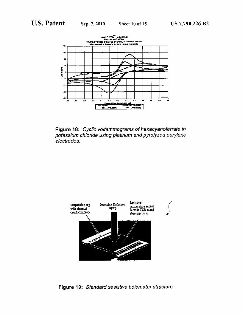
Thin-film pyrolyzed parylene-C electrodes were fabricatedusing room temperature polymer vapor deposition onto aSi/S'02 substrate. The electrodes were pyrolyzed in a nitro-gen atmosphere then patterned using Oz plasma. The 900Degrees Celsius electrodes were then isolated with a secondparylene layer and metal contacts were deposited. FIG. 18shows cyclic voltammograms of 5 mM in 0.1 M KCl forvarious processing parameters of the pyrolyzed parylene aswell as a scan using a Pt electrode for comparison. Improve-ments in electrode kinetics, evident by a reduction in peak-to-peak separation, can be observed as carbonization tem-perature and film thickness are increased.
Although the above has been described in terms of specificembodiments, there can be other variations, modifications,and alternatives. These and other variations will be furtherdescribed throughout the present specification and more par-ticularly below.
Bolometer DesignsIn a specific embodiment, the present invention provides a
method and apparatus for a bolometer design. More particu-larly, the invention provides a method and system for anuncooled, room-temperature, all parylene bolometer device.The device includes two layers of pyrolyzed (or "carbon-
ized") parylene and a metal layer for interconnections accord-ing to a specific embodiment. Other embodiments mayinclude a single layer of pyrolyzed parylene. We demon-strated that high responsivity can be achieved by tailoring theelectrical conductivity and the temperature coefficient ofresistance (TCR) using different pyrolysis conditions foreach parylene layer. Further details of the present device andmethods of manufacture can be found throughout the presentspecification and more particularly below.
FIG. 19 is a simplified diagram of a bolometer sensingdevice 1900 according to an embodiment of the presentinvention. This diagram is merely an example, which shouldnot unduly limit the scope of the claims herein. One of ordi-nary skill in the art would recognize many variations, modi-fications, and alternatives. As shown, the sensing device is aresistive uncooled bolometer. The device has a free-standingtemperature-sensitive element that is linked to a substrate bylow thermal conductance legs. As merely an example, Equa-tion (1) shows the expression of the direct current responsiv-ity (in Volts per incident Watt) for such a device.
DV aRle;,,h (1)A(V.W-i)= P = C
where a is the TCR of the sensing element. R is the bolometerresistance, G is the pixel-to-substrate thermal conductanceand ,q is the bolometer absorptance. The thermal time con-stant is given by:
16
(2)T (S) = C,
where C is the thermal capacitance. Preferably, a desirableparameters to obtain good responsivity are: high pixel-TCRand low pixel to-substrate thermal conductance. However, as
io we try to decrease the thermal conductance, we must be ableto decrease the thermal conductance. Most conventionaluncooled bolometers use vanadium oxide [see P. E. Howardet al Proc. SPIE Vol. 3698 131 (1999)] or amorphous silicon[see Tissot J L, Infrared Physics & Technology 43 (3-5)
15 223-228 June-October 2002] as temperature-sensitive mate-rial, reaching a TCR of about 1.5% to 3%. Another possiblematerial is YBaCuO [see A Semiconductor YBaCuOMicrobolometer for Room Temperature IR Imaging," A. Jah-anzeb, C. M. Travers, Z. Celik-Butler, D. P. Butler, and S. Tan,
20 IEEE Transactions on Electron Devices, vol. 44, pp. 1795-1801, 1997]. The suspension legs are usually made of siliconnitride or polysilicon. In the case of silicon nitride legs, it isnecessary to have another layer for electrical conduction.Here, a bolometer is proposed using pyrolyzed parylene both
25 for the temperature -sensing element and for the suspensionlegs according to a specific embodiment.
Certain properties of pyrolyzed parylene are described.Pyrolyzed parylene as a MEMS "sacrificial' material wasreported by Hui et al in 1998 [see E. E. Hui, C. G. Keller, and
3o R. T. Howe, "Carbonized parylene as a conformal sacrificiallayer", 8th Solid-State Sensor and Actuator Workshop Tech-nical Digest Hilton Head, 1998, pp. 256-260] in which car-bonized parylene is subsequently burned away in O z environ-ment at high temperature. Other than that, it is also known that
35 pyrolysis of polymers can lead to electrically conductive orpartial conductive films [see E. E. Hui, C. G. Keller, and R. T.Howe, "Carbonized parylene as a conformal sacrificiallayer", 8th Solid-State Sensor and Actuator Workshop Tech-nical Digest Hilton Head, 1998, pp. 256-260]. Interestingly,
40 the electrical conductivity of pyrolyzed parylene can beadjusted over a very wide range (from insulating downto =10-2 Q-cm) depending on the pyrolysis conditions [see S.Konishi M. Liger, T. A. Harder and Y. C. Tai, to be publishedin IEEE MEMS104 Technical Digest]. The temperature
45 dependence of the resistance of pyrolyzed parylene films wasstudied. FIG. 21 shows the temperature dependence of theresistance of a sample having a resistivity of 1.9 * 10 3 Q-cm atroom temperature. As can be seen on this figure, the conduc-tivity follows an Arrehnius dependence:
S^-,*e Ea/(2)
where a Ea is the activation energy.For a resistivity having anArrehnius dependence, the tem-
55 perature coefficient of resistance (TCR) is given by,
(3)a= -kV,
60
Like other materials often used in uncooled infrared sen-sors (vanadium oxide and amorphous silicon), the TCR ofpyrolyzed parylene increases with resistivity. FIG. 22 showsthe TCR of various films having different resistivities (ob-
65 tained by pyrolysis at different temperatures). The TCR ofpyrolyzed-parylene does show a logarithmic dependence onthe resistivity. The measured TCR was —4%/K for films hav-
US 7,790,226 B2
17ing -10$ Q-cm resistivity down to -0.3%/K for filmshaving -10-2 Q-cm resistivity. The corresponding activationenergies are 0.023 eV and 0.31 eV respectively. Becausehigher bolometer resistance leads to higher thermal noise,there is a trade-off between high responsivity (given by highTCR) and signal-to-noise ratio (given by low resistance).
While measuring the temperature dependence of the filmsin air, it was found that the resistivity of pyrolyzed parylene issensitive to moisture. Therefore, the TCR measurementswere performed in a vacuum chamber. FIG. 22 shows theresistance drop of a pyrolyzed-parylene film when exposed toair after being stabilized in vacuum. This resistance change isreversible. However, this sensitivity to moisture is not a prob-lem for our application since uncooled bolometers operate invacuum (for thermal insulation purposes).
Since our ultimate goal is the build an uncooled IR focal-plane array, the bolometer design is similar to that shown onFIG. 19. The pixel size was chosen to be 50x50 µm2, astandard size allowing acceptable resolution with a chip-sized array. For this geometry, the total pixel resistance isgiven by:
R=2R i,+R,jXev (4)
assuming we can neglect contact resistances. Upon incomingradiation, most of the temperature increase occurs on thepixel. Therefore, to maximize the relative change in totalresistance, the resistance of the pixel must be dominant overthe resistance of the suspension legs. However, with such alayout, it is obvious that the number of electrical "squares" ofthe suspension legs is greater than that of the pixel (=1). Forthat reason, the sheet resistance of the suspensions legs mustbe much smaller than the sheet resistance of the pixel. Theprocess-tunablity of the properties of pyrolyzed-paryleneallows us to fabricate a bolometer meeting this requirementwith a simple two-layers process. To allow comparison withVOx-based bolometers the target TCR was set around -2%,which according to FIG. 21 would be obtained fora resistivityin the order of 102 Q-cm. The width of the suspensions legswas designed to be 5 µm and their lengths varied from 50 µmto 170 µm, corresponding to a number of resistor squaresvarying from 10 to 34. Therefore, for the total bolometerresistance to be dominated by the pixel resistance, the resis-tivity of the suspension legs should be on the order of 10-i to10-2 Q-cm (if the thicknesses are comparable).
A method of fabricating a bolometer sensing deviceaccording to an embodiment of the present invention can beprovided below.1. Provide a substrate (e.g., silicon wafer) comprising a sur-
face region;2. Form an insulating material overlying the surface region;3. Form a film of carbon based material overlying the insu-
lating material;4. Treat the film of carbon based material to pyrolyzed the
carbon based material;5. Cause formation of a film of substantially carbon based
material having a resistivity ranging within a predeter-mined range based upon at least the treatment;
6. Form an interconnect layer overlying the pyroyzed carbonbased material;
7. Form a gap underlying a portion of pyrolyzed carbon basedmaterial;
8. Perform other steps, as desired.The above sequence of steps provides a method according
to an embodiment of the present invention. As shown, themethod uses a combination of steps including a way of form-ing a bolometer sensing device using a pyrolyzed parylene
18bearing material or the like. Other alternatives can also beprovided where steps are added, one or more steps areremoved, or one or more steps are provided in a differentsequence without departing from the scope of the claims
5 herein. Further details of the present method and structure canbe found throughout the present specification and more par-ticularly below.
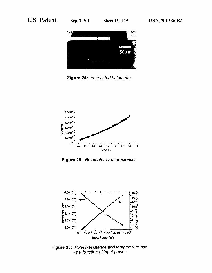
One device process, FIG. 23, begins with a 5000 A oxidegrowth and patterning. A 3 µm-thick parylene-C layer is then
io deposited and pyrolyzed in a nitrogen atmosphere. The tem-perature is raised to 800° C. at 10° C./min then cooled downto room temperature at 2° C./min. The resulting film is pat-terned to define the suspension legs. The pyrolyzed-paryleneetching is done in a Technics PEII plasma etcher with 400 W,
15 200 mT of Oz using a photoresist mask. The etching rate ofpyrolyzed-parylene was found to be comparable to that ofparylene (-1800 Amin) for these same settings. A secondlayer ofparylene (0.8 µm) is deposited, and then pyrolyzed at660° C. (with the same ramping parameters as previously).
20 For better repeatability, the samples are being kept at thepyrolysis temperature for 2 hours. The second layer of pyro-lyzed parylene is patterned define the pixel area. In a certainembodiment, the pyrolyzed parylene sensing element isdeposited on a sacrificial layer, which is subsequently etched
25 away to form a free standing portion of the pyrolyzedparylene sensing element. Depending upon the specificembodiment, the sacrificial layer can be made of a suitablematerial such as amorphous silicon, polysilicon, metal,organic material, or other materials, or combination of mate-
3o rials depending upon the specific application. Next, a Ti/Auinterconnection layer (60 A2000 A) is evaporated and pat-terned. Finally, the bolometers are released by XeF 2 gas-phase etching. FIG. 24 shows a fabricated free-standingdevice.
35 Typically, parylene depositions involve a prior coating ofA174 for adhesion promotion [see Product Specifications,A-174 Silane Promotion, Specialty Coating Systems, Inc.,Indianapolis, Ind., Phone: (800) 356-8260.]. However, it wasfound that this procedure leads to poor adhesion of the films
4o after pyrolysis. On the other hand, the adhesion of pyrolyzedparylene on SiO z/Si wafers that have not been coated withAl 74 was excellent. This is also part of the reasons why it waschosen to pattern the parylene after pyrolysis rather than theopposite. It was also observed that pyrolysis of patterned
45 parylene leads to undesirable border effects, probably due tothe pyrolysis-induced stress. Finally, due to the isotropicetching, patterning the parylene after it has been shrunk (4 to5 times) by pyrolysis minimizes undercut.
Sheet resistance and contact resistance were measured by50 Greek-cross structures. The contact between the pyrolyzed
parylene layers and Ti/Au was found to be ohmic with aspecific contact resistance of 3.5x10 -3 Q . CM2 for first layerand 3.5 Q . CM2 for the second layer. The contact between thefirst and the second layer of pyrolyzed parylene was also
55 ohmic with a specific contact resistance of 1.57 Q . CM2 . TheTCR of the second parylene layer around room temperaturewas measured to be -1.63%/K. Table (1) shows differentcharacteristics of interest for the two pyrolyzed-parylene lay-ers. The ratio between the sheet resistance of the first and the
60 second layer is 8.7x10³ . Therefore, for the chosen geom-etries, the total resistance of the bolometers is indeed domi-nated by the temperature-sensing element obtained from thesecond layer of pyrolyzed parylene.
After wire-bonding and packaging, the bolometers were65 placed in a vacuum chamber (<1 mT) and stabilized for
several hours to eliminate any potential moisture-relateddrift. Current-Voltage characteristics of the bolometers were
US 7,790,226 B219
20measured with an HP4145 working as a voltage source/cur-rent monitor. A hold time of 1 second was used at each bias toensure thermal steady-state. FIG. 25 shows the IV curve for a50x50 µm2 bolometer with two 5 µmx170 M suspensionsbeams. The upward curvature seen on this figure indicatesself-heating (the TCR of pyrolyzed-parylene being negative).Unreleased bridges do not exhibit this self-heating.
FIG. 26 shows the resistance and temperature rise as afunction of input power. The temperature rise is calculatedfrom the resistance change and TCR. The corresponding ther-mal conductance is 5.43x10 -$ WK- '. Knowing the dimen-sions of the legs, we can estimate the thermal conductivity ofthe first layer of pyrolyzed parylene to be KPP=1.5 Wm-'.K-1. Similar calculations on other bolometers having differ-ent geometries (smaller suspensions legs) lead to lower ther-mal conductivities 1.5 W•rn '•K- '<KPP<l.I W•rn '•K- '. Thisis comparable to values reported for PECVD silicon nitride[See, M. Von Arx, O. Paul and H. Baltes, JMEMS Vol. 9. No.1 March 2000 136-145; and S. Hafizovic, O. Paul, Sensorsand Actuators A 97-98 (2002) 246-252] and lower thanLPCVD nitride, with the major advantage of providing elec-trical conductivity. It is also one order of magnitude lowerthan polysilicon [Angela D., et al. "Thermal conductivity ofdoped polysilicon layers", Journal of Microelectricalme-chanical Systems, Vol. 10 (3), September 2001 360-369.]From the TCR and the thermal conductance, we can expectthe responsivity to be R=3*105 * ,q(for a 1 Volt bias, and 5ltmx170 µm suspension legs), where q is the absorptance ofthe pixel. Although the sensitivity to incoming radiation wasqualitatively observed, the absorptance of pyrolyzed parylenethin films for the wavelengths of interest (e.g. 8 µm to 14 µmfor thermal imaging) still needs to be characterized. However,because of the carbon-like properties of pyrolyzed parylene,we can expect the absorptance to be close to 1.
Uncooled infrared sensors have been successfully demon-strated with a simple two-layer pyrolyzed-parylene process.Electro thermal study shows that pyrolyzed-parylene is apromising candidate to replace silicon nitride and polysiliconfor the thermal insulation, while it can also be used to achievehigh-TCR thin films for the pixel. IR optical characterizationas well as dynamic behavior is currently underway. Addi-tional embodiments include the development of a purely sur-face-micromachining process, and the fabrication of a bolom-eter array.
In a specific embodiment, the bolometer design can havecertain other features according to the present invention. Thatis, the bolometer has a substrate as noted above that is freefrom any cooling element, which is associated with drawingoff heat from electron hole interactions. Here, the increase intemperature on each of the carbon based regions is fromradiation influence. In certain embodiments, the interconnec-tion of the bolometer acts as a heat sink. Depending upon theembodiment, certain colors are desired in the sensor regions,e.g., carbon based regions. That is, the carbon based materialregions comprises a substantially black color to increase aradiation influence.
Also depending upon the specific embodiment, the array ofsubstantially carbon based regions is packaged and main-tained in a vacuum. In a specific embodiment, the vacuum isless than 20 millitorr but can be at other vacuums or partialvacuums. Other packaging designs also provide that the sub-stantially carbon based regions is free from any coatings suchas antireflection coating. The bolometer may also include atransparent member overlying the array of substantially car-bon based material regions, which is maintained in thevacuum. The transparent member comprises a germanium,
sapphire, calcium fluoride, zinc zelenide, zinc sulfide,AMTIR, or other alloy to allow infrared radiation accordingto specific embodiments.
Although the above has been described in terms of specific5 embodiments, there can be other variations, modifications,
and alternatives. In a specific embodiment, the predeterminedrange is from about 10$ Ohms-cm to about 10` Ohms-cm,other ranges can also exist, which are within our outside of thepredetermined range. Additionally, each of the carbon based
10 regions in the bolometer design may have a dimension of lessthan 100 µm and an area of less than 10-2 cm2, although otherdimensions can also exist according to other embodiments.
Additional Embodiments 1-6115
1. Apparatus for sensing electromagnetic radiation usingcarbon based sensing materials, the apparatus comprising:
a substrate comprising a surface region;an array of substantially carbon based material regions
20 having a resistivity ranging within a predetermined rangedisposed overlying the surface, each of the carbon basedmaterial regions comprising a portion being suspended over aregion of the surface to thermally insulate the portion of thesuspended carbon based material;
25 an insulating region formed between the region and theportion of the carbon based material; and
an interconnection to coupled to each of the carbon basedmaterial regions;
30 one or more nodes coupled to the interconnection, the oneor more nodes being able to independently read a resistivityvalue associated at least one or more of the carbon basedmaterial regions.
2. The apparatus of embodiment 1 wherein the predeter-35 mined range is from about 10 $ Ohms cm to about 10-3 Ohms
cm.3. The apparatus of embodiment 1 wherein the apparatus is
a bolometer.4. The apparatus of embodiment 1 wherein the carbon
4o based material comprises amorphous carbon bearing mate-rial.
5. The apparatus of embodiment 1 wherein the carbonbased material comprises pyrolyzed parylene, polyimide,photoresist, or other polymers.
45 6. The apparatus of embodiment 1 wherein the intercon-nection comprises a metal layer.
7. The apparatus of embodiment 1 wherein the substratecomprises silicon bearing material.
8. The apparatus of embodiment 1 wherein each of theSo carbon based material regions is apixel element foraplurality
of pixel regions.9. The apparatus of embodiment 1 wherein the insulating
region is at least 2.5 µm in dimension from the surface of the
55 region to the portion of the carbon based material.
10. The apparatus of embodiment 1 wherein the insulatingregion comprises an air gap.
11. The apparatus of embodiment 1 wherein each of thecarbon based regions has a dimension of less than 100 µm.
60 12. The apparatus of embodiment 1 wherein one or more ofthe carbon based regions has an area of less than 10 -2 cm2.
13. The apparatus of embodiment 1 wherein the substrate isselected from silicon, silicon on insulator, other semiconduc-tor materials, glass, quartz, metal or organic materials.
65 14. The apparatus of embodiment 1 wherein each of thecarbon based regions is characterized by a thickness andsurface area.
US 7,790,226 B221
15. The apparatus of embodiment 14 wherein the surfacearea is less than about 10 -2 cm2 and the thickness is less thanabout 2µm.
16. The apparatus of embodiment 1 wherein each of thecarbon based regions may change in resistivity value uponreceiving a dosage of electromagnetic radiation.
17. The apparatus of embodiment 1 wherein the sensor isun-cooled.
18. The apparatus of embodiment 1 wherein the electro-magnetic radiation is 8-14 micron wavelength band.
19. The apparatus of embodiment 1 wherein the electro-magnetic radiation is in the 3-5 micron band.
20.The apparatus of embodiment 1 whereinthe substrate isfree from any cooling element, the cooling element beingassociated with drawing off heat from electron hole interac-tions.
21. The apparatus of embodiment 1 wherein the increase intemperature is from radiation influence.
22. The apparatus of embodiment 1 wherein the intercon-nection acts as a heat sink.
23. The apparatus of embodiment 1 wherein the carbonbased material regions comprises a substantially black colorto increase a radiation influence.
24. The apparatus of embodiment 1 wherein the array ofsubstantially carbon based regions is packaged and main-tained in a vacuum.
25. The apparatus of embodiment 24 wherein the vacuumis less than 20 millitorr.
26. The apparatus of embodiment 1 wherein the substan-tially carbon based regions is free from any coatings.
27. The apparatus of embodiment 1 wherein the substan-tially carbon based material comprises an antireflection coat-ing.
28. The apparatus of embodiment 1 further comprising atransparent member overlying the array of substantially car-bon based material regions.
29. The apparatus of embodiment 28 wherein the transpar-ent member comprises a germanium, sapphire, calcium fluo-ride, zinc zelenide, zinc sulfide, AMTIR, or other alloy toallow infrared radiation.
30. The apparatus of embodiment 1 further comprising asubstantially carbon based interconnect coupled to each ofthe regions, the substantially based interconnect being char-acterized by a first resistivity value and each of the regionsbeing characterized by a second resistivity value.
31. A method for fabricating a sensing device, the methodcomprising:
providing a substrate comprising a surface region;forming an insulating material overlying the surface
region;forming a film of carbon based material overlying the
insulating material; andtreating to the film of carbon based material to pyrolyzed
the carbon based material to cause formation of a film ofsubstantially carbon based material having a resistivity rang-ing within a predetermined range; and
forming a gap underlying a portion of pyrolyzed carbonbased material.
32. The method of embodiment 31 wherein the predeter-mined range is from about 10 $ Ohm-cm to about 103 Ohm-cm.
33. The method of embodiment 1 wherein the carbon basedmaterial is Parylene, photo resist, or other polymer.
34. The method of embodiment 31 wherein the pyrolyzedcarbon based material is Pyrolyzed parylene.
35. The method of embodiment 31 wherein the treatingcomprises thermally treating the carbon based material.
2236. The method of embodiment 31 further comprising
maintaining the film of carbon based material in an inertenvironment during a portion of time of the treatment.
37. The method of embodiment 31 wherein the forming of5 the gap is provided by an etching process to release the
portion of the pyrolyzed carbon based material from a portionof the insulating material.
38. The method of embodiment 1 wherein the gap com-prises an airgap.
10 39. The method of embodiment 31 further comprisingforming a first interconnect structure overlying a first contactregion of the pyrolyzed carbon based material and a secondinterconnect structure overlying a second contact region ofthe pyrolyzed carbon based material.
15 40. The method of embodiment 39 wherein the first inter-connect structure and the second interconnect structure com-prise metallization.
41. The method of embodiment 40 wherein the forming thegap occurs after forming the first interconnect structure and
20 the second interconnect structure.42. The method of embodiment 31 wherein the sensing
device is a bolometer.43. The method of embodiment 31 wherein the pyrolyzed
25 carbon based material comprises amorphous carbon bearingmaterial.
44. The method of embodiment 31 wherein the pyrolyzedcarbon based material comprises Pyrolyzed Parylene, photo-resist, or other polymer.
30 45. The method of embodiment 31 wherein the substratecomprises silicon bearing material.
46. The method of embodiment 31 wherein the pyrolyzedcarbon based material is fora pixel element from a plurality ofpixel regions.
35 47. The method of embodiment 31 wherein the insulatingmaterial is at least 1000 Angstrom in dimension.
48. The method of embodiment 31 wherein the pyrolyzedcarbon based material changes in resistivity upon receiving aincreased dosage of electromagnetic radiation from a first
4o resistivity value to a second resistivity value.49. The method of embodiment 48 wherein the electro-
magnetic radiation reduces the first value to the second value.50. The method of embodiment 31 wherein each of the
regions is a pixel element, each of the pixel elements being45 characterized by a size of is 50 microns and less.
51. Apparatus for chemical sensing using carbon basedsensing materials, the apparatus comprising:
a pyrolyzed parylene carbon based electrode structure hav-ing a resistivity ranging within a predetermined range, the
So electrode having a first end coupled to a second end and alength defined between the first end and the second end;
an interconnect coupled to at least one of the ends.52. The apparatus of embodiment 51 wherein the predeter-
55 mined range is from about 10 $ Ohm-cm to about 103 Ohm-cm.
53.The apparatus of embodiment 51 wherein the apparatusis a chemical sensor.
54. The apparatus of embodiment 51 wherein the pyro-60 lyzed parylene carbon based material comprises amorphous
carbon bearing material.55. The apparatus of embodiment 51 wherein the intercon-
nection comprises a metal layer.56. The apparatus of embodiment 51 wherein the pyro-
65 lyzed parylene carbon based electrode structure may changein an electrical characteristic upon exposure of one or morechemical species.
US 7,790,226 B223
57. The apparatus of embodiment 51 further comprising areference electrode coupled to the pyrolyzed parylene carbonbased electrode structure.
58. The apparatus of embodiment 7 wherein the referenceelectrode is made of a metal material.
59. The apparatus of embodiment 8 wherein the metalmaterial is selected from gold, platinum, copper, aluminum ornickel.
60.A method for fabricating a sensing device, the methodcomprising:
providing a substrate comprising a surface region;forming an insulating material overlying the surface
region;
forming a film of carbon based material overlying theinsulating material; and
treating to the film of carbon based material to pyrolyzedthe carbon based material to cause formation of a film ofsubstantially carbon based material having a resistivity rang-ing within a predetermined range;
providing at least a portion of the pyrolyzed carbon basedmaterial in a sensor application;
using the portion of the pyrolyzed carbon based material inthe sensing application.
61. The method of embodiment 60 wherein the sensingapplication is selected from chemical, humidity, mechanicalstrain or temperature.
What is claimed is:1. A method of carbon thin film deposition comprising:depositing a catalyst on a substrate;depositing a hydrocarbon polymer film on the substrate in
contact with the catalyst, wherein the hydrocarbon poly-mer film is a parylene film; and
pyrolyzing the hydrocarbon polymer film to form a carbonthin film, wherein the pyrolyzing comprises raising thetemperature of the hydrocarbon polymer film to a tem-perature where it decomposes and holding it there for atime to produce the carbon thin film, wherein the tem-perature is about 500° C. to about 900° C. and the resis-tivity of the carbon film is less than 1x10 10 Q-cm.
2. A method of carbon thin film deposition comprising:depositing a catalyst on a substrate, wherein the catalyst is
Ti/Pt or Cr/Au;depositing a hydrocarbon polymer film on the substrate in
contact with the catalyst; andpyrolyzing the hydrocarbon polymer film to form a carbon
thin film, wherein the pyrolyzing comprises raising thetemperature of the hydrocarbon polymer film to a tem-perature where it decomposes and holding it there for atime to produce the carbon thin film, wherein the tem-perature is about 500° C. to about 900° C. and the resis-tivity of the carbon film is less than 1x10 10 Q-cm.
3. A method of making of carbon containing patternedstructure comprising:
depositing a hydrocarbon polymer film on a substrate,wherein the hydrocarbon polymer film is a parylenefilm;
pyrolyzing the hydrocarbon polymer film to form a carbonthin film, wherein the pyrolyzing comprises raising thetemperature of the hydrocarbon polymer film to a tem-perature where it decomposes and holding it there for atime to produce the carbon thin film, wherein the tem-perature is about 500° C. to about 900° C. and the resis-tivity of the carbon film is less than 1x10 10 Q-cm; and
patterning the carbon thin film.4. A method of making carbon containing patterned struc-
ture comprising:
24depositing a hydrocarbon polymer film on a substrate,
wherein the hydrocarbon polymer film is a parylenefilm;
patterning the hydrocarbon polymer film; and5 pyrolyzing the patterned hydrocarbon polymer film to
form a carbon containing patterned structure, whereinthe pyrolyzing comprises raising the temperature of thehydrocarbon polymer film to a temperature where itdecomposes and holding it there for a time to produce
10 the carbon structure, wherein the temperature is about500° C. to about 900° C. and the resistivity of the carbonstructure is less than 1 x10 10 Q-cm.
5. A method of carbon thin film formation to provide goodadhesion between the carbon thin film and a substrate com-
15 prisingdepositing a parylene film on a substrate, wherein the sub-
strate does not comprise a prior coating of gamma-meth-acryloxypropyltrimethoxy silane (A174); and
pyrolyzing the parylene film to form a carbon thin film^^ adhered to the substrate, wherein said pyrolyzing com-
prises raising the temperature of the film to a tempera-ture from about 500'C. to about 900'C. where it decom-poses and holding it there for a time to produce thecarbon thin film, wherein the resistivity of the carbon
25 film is less than 1 x10 10 Q-cm.6. The method of claim 5, wherein the substrate is silicon,
quartz, glass or metal.7. The method of claim 5, wherein pyrolyzing the parylene
30 film is performed in presence of a catalyst.8. The method of claim 7, wherein the catalyst is metal.9. The method of claim 8, wherein the catalyst comprises
nickel, iron, cobalt, platinum, ferrocene, titanium, chrome,gold, ferric nitrate, or a combination thereof.
35 10. The method of claim 7, wherein the catalyst is Ti/Pt orCr/Au.
11. The method of claim 5, wherein pyrolyzing theparylene film is performed in an atmosphere of argon, oxy-gen, or hydrogen.
40 12. The method of claim 5, wherein pyrolyzing theparylene film is performed in an atmosphere of nitrogen.
13. The method of claim 5 further comprising patterningthe carbon thin film.
45 14. The method of claim 13, wherein patterning the carbonthin film is done by plasma etching.
15. The method of claim 5, wherein parylene film is apatterned film.
16. A method of carbon thin film deposition comprising:50 depositing a catalyst on a substrate;
depositing a hydrocarbon polymer film on the substrate incontact with the catalyst; and
pyrolyzing the hydrocarbon polymer film to form a carbon55 thin film, wherein the pyrolyzing comprises raising the
temperature of the hydrocarbon polymer film to a tem-perature where it decomposes and holding it there for atime to produce the carbon thin film, wherein the tem-perature is about 500° C. to about 900° C., wherein the
60 resistivity of the carbon film is less than 1 x10 10 Q-cm,and wherein the carbon film is an amorphous carbonfilm.
17. A method of carbon thin film deposition comprising:depositing a catalyst on a substrate, wherein the depositing
65 is carried out at room temperature;depositing a hydrocarbon polymer film on the substrate in
contact with the catalyst; and

US 7,790,226 B225 26
pyrolyzing the hydrocarbon polymer film to form a carbon perature is about 500° C. to about 900° C., wherein the
thin film, wherein the pyrolyzing comprises raising the resistivity of the carbon film is less than 1 x10 10 Q-cm.temperature of the hydrocarbon polymer film to a tem-perature where it decomposes and holding it there for atime to produce the carbon thin film, wherein the tem-