msp50c3x user's guide' - analog, embedded processing, … · · 2011-08-06chapter 3...
TRANSCRIPT
User’s Guide
Mixed-Signal Products2000SPSU006C
IMPORTANT NOTICE
Texas Instruments and its subsidiaries (TI) reserve the right to make changes to their productsor to discontinue any product or service without notice, and advise customers to obtain the latestversion of relevant information to verify, before placing orders, that information being relied onis current and complete. All products are sold subject to the terms and conditions of sale suppliedat the time of order acknowledgment, including those pertaining to warranty, patent infringement,and limitation of liability.
TI warrants performance of its semiconductor products to the specifications applicable at thetime of sale in accordance with TI’s standard warranty. Testing and other quality controltechniques are utilized to the extent TI deems necessary to support this warranty. Specific testingof all parameters of each device is not necessarily performed, except those mandated bygovernment requirements.
Customers are responsible for their applications using TI components.
In order to minimize risks associated with the customer’s applications, adequate design andoperating safeguards must be provided by the customer to minimize inherent or proceduralhazards.
TI assumes no liability for applications assistance or customer product design. TI does notwarrant or represent that any license, either express or implied, is granted under any patent right,copyright, mask work right, or other intellectual property right of TI covering or relating to anycombination, machine, or process in which such semiconductor products or services might beor are used. TI’s publication of information regarding any third party’s products or services doesnot constitute TI’s approval, warranty or endorsement thereof.
Copyright 2000, Texas Instruments Incorporated
iii Read This First
Preface
Read This First
About This Manual
This manual describes the MSP50x3x family of speech synthesizing devices.When necessary, the differences between the family members are shown inseparate and consecutive sections. The object of this user’s guide is to providethe information needed to implement a speech synthesizer design using aMSP50x3x devices.
How to Use This Manual
This document contains the following chapters:
Chapter 1 Introduction to the MSP50x3x FamilyThis chapter describes the MSP50x3x family features, D/A options, pin as-signments and descriptions, and gives a brief introduction to linear predic-tive coding.
Chapter 2 MSP50x3x Family ArchitectureThis chapter describes the architecture of the MSP50x3x family with aseparate sections for speech synthesis, interrupts, power control, initial-ization, and clocks. For the MSP50x37, there are separate sections for theanalog-to-digital converter and the power amplifier.
Chapter 3 MSP50x3x AssemblerThis chapter contains a detailed description of the MSP50x3x assembler.
Chapter 4 MSP50x3x Instruction SetThis chapter provides the instruction set for the MSP50x3x.
Chapter 5 MSP50x3x ApplicationsThis chapter describes various hints and useful advice for designing ap-plications for the MSP50x3x.
Running Title—Attribute Reference
iv
Chapter 6 Customer InformationThis chapter describes customer information including developmentcycles structure, speech development/production sequence, mechanicalinformation, and ordering information.
Appendix A Script Preparation and Speech Development ToolsThis appendix describes script preparation and development tools for theMSP50x3x.
Appendix B MSP50C3x Versus TSP50C1xThis appendix contains information about switching from a TSP50C1xfamily device to a MSP50C3x family device
Appendix C MSP50x3x Sample Dual Synthesis ProgramThis appendix contains a sample dual synthesis program that uses bothLPC channels to speak an echo.
Appendix D Sample Synthesis ProgramThis appendix contains a sample synthesis program that counts numbersfrom one to five on one channel only.
Appendix E MSP50C3x Data SheetThis appendix contains the data sheet for the MSP50C3x family of de-vices. This data sheet lists the absolute maximum operating condition,recommended operation conditions, and the electrical characteristics forthe MSP50C3x devices.
Notational Conventions
v Read This First
Notational Conventions
This document uses the following conventions.
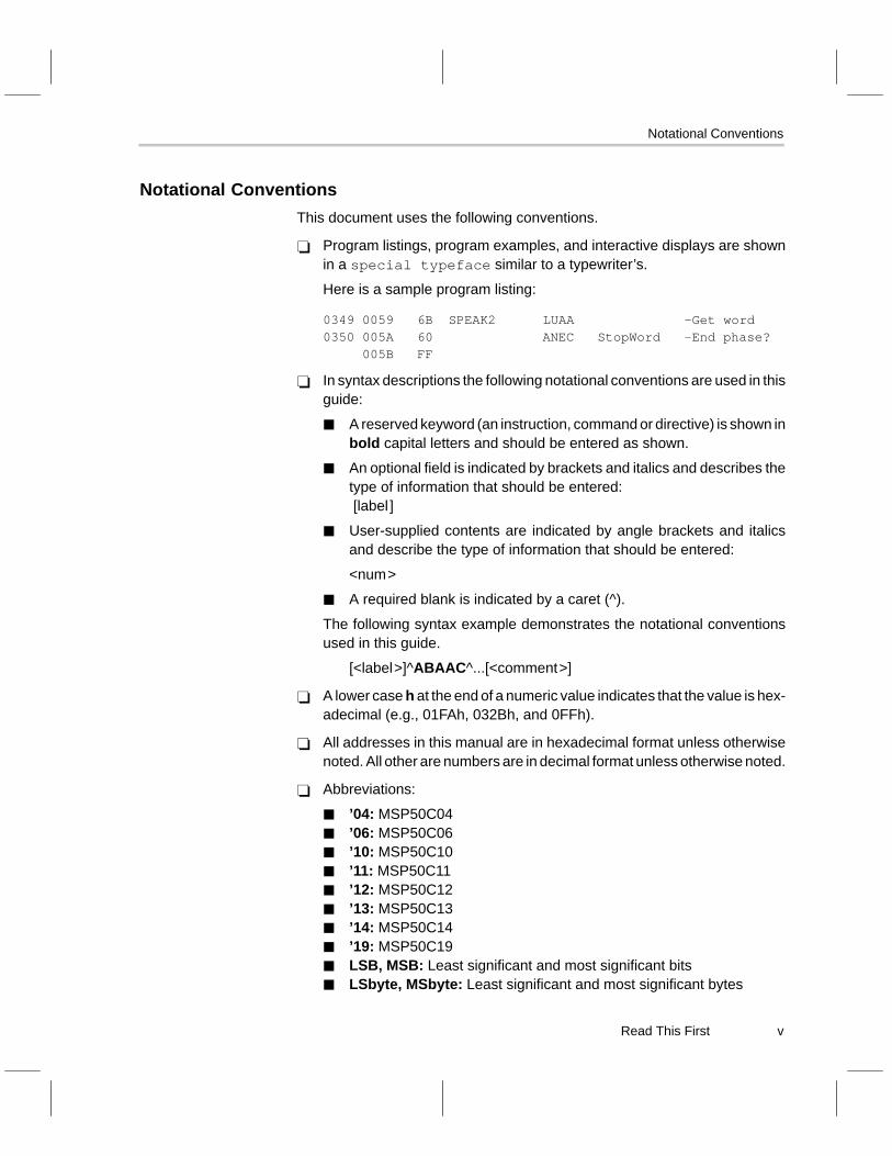
Program listings, program examples, and interactive displays are shownin a special typeface similar to a typewriter’s.
Here is a sample program listing:
0349 0059 6B SPEAK2 LUAA –Get word0350 005A 60 ANEC StopWord –End phase?
005B FF
In syntax descriptions the following notational conventions are used in thisguide:
A reserved keyword (an instruction, command or directive) is shown inbold capital letters and should be entered as shown.
An optional field is indicated by brackets and italics and describes thetype of information that should be entered: [label ]
User-supplied contents are indicated by angle brackets and italicsand describe the type of information that should be entered:
<num>
A required blank is indicated by a caret (^).
The following syntax example demonstrates the notational conventionsused in this guide.
[<label>]^ABAAC^...[<comment>]
A lower case h at the end of a numeric value indicates that the value is hex-adecimal (e.g., 01FAh, 032Bh, and 0FFh).
All addresses in this manual are in hexadecimal format unless otherwisenoted. All other are numbers are in decimal format unless otherwise noted.
Abbreviations:
’04: MSP50C04 ’06: MSP50C06 ’10: MSP50C10 ’11: MSP50C11 ’12: MSP50C12 ’13: MSP50C13 ’14: MSP50C14 ’19: MSP50C19 LSB, MSB: Least significant and most significant bits LSbyte, MSbyte: Least significant and most significant bytes
Information About Cautions
vi
Port A refers to pins PA0 — PA7 operating together.
Port B refers to pins PB0 and PB1 operating together.
Individual bits of a register are indicated with the register abbreviation fol-lowed by a decimal point and the bit number (e.g., bit 5 of the A registeris A.5 or bit 2 of the mode register is MR.2).
*X is the contents of the location pointed to by the address stored inX register.
A’ indicates the old contents of the A register
Information About Cautions
This book may contain cautions.
This is an example of a caution statement.
A caution statement describes a situation that could potentiallydamage your software or equipment.
The information in a caution is provided for your protection. Please read eachcaution carefully.
If You Need Assistance
vii Read This First
If You Need Assistance . . .
If you want to . . . Contact Texas Instruments at . . .
Visit TI online World Wide Web: http://www.ti.com
Receive general information World Wide Web: http://www.ti.com/sc/docs/pic/home.htmor assistance North America, South America: (972) 644–5580
Europe, Middle East, AfricaDutch:
English:French:Italian:
German:
33–1–3070–116633–1–3070–116533–1–3070–116433–1–3070–116733–1–3070–1168
Japan (Japanese or English)Domestic toll-free:
International:0120–81–002681–3–3457–0972 or81–3–3457–0976
Korea (Korean or English): 82–2–551–2804
Taiwan (Chinese or English): 886–2–3771450
Request more informationabout Texas InstrumentsSpeech Synthesizerproducts
World Wide Web: http://www.ti.com/sc/speech
Order Texas Instrumentsdocumentation (see Note 1)
Literature Response Center: (800) 477–8924
Make suggestions about or Email: [email protected] errors in documenta-tion (see Note 2)
Mail: Texas Instruments IncorporatedTechnical Publications Manager, MS 8711P.O. Box 655303Dallas, Texas 75265–5303
Notes: 1) The literature number for the book is required; see the lower-right corner on the back cover.
2) Please mention the full title of the book, the literature number from the lower-right corner of the back cover, and thepublication date from the spine or front cover.
Trademarks
IBM, PC, PC/XT, PC/AT are trademarks of IBM Corporation.TI is a trademark of Texas Instrument Incorporated.

viii
Contents
ix
Contents
1 Introduction to The MSP50x3x Family 1-1. . . . . . . . . . . . . . . . . . . . . . . . . . . . . . . . . . . . . . . . . . . . . 1.1 MSP50x3x Device Family 1-2. . . . . . . . . . . . . . . . . . . . . . . . . . . . . . . . . . . . . . . . . . . . . . . . . . . . 1.2 Applications 1-3. . . . . . . . . . . . . . . . . . . . . . . . . . . . . . . . . . . . . . . . . . . . . . . . . . . . . . . . . . . . . . . . 1.3 Description 1-4. . . . . . . . . . . . . . . . . . . . . . . . . . . . . . . . . . . . . . . . . . . . . . . . . . . . . . . . . . . . . . . . 1.4 Features 1-6. . . . . . . . . . . . . . . . . . . . . . . . . . . . . . . . . . . . . . . . . . . . . . . . . . . . . . . . . . . . . . . . . .
1.4.1 MSP50x32/33/34 Additional Features 1-6. . . . . . . . . . . . . . . . . . . . . . . . . . . . . . . . . . 1.4.2 MSP50x37 Additional Features 1-7. . . . . . . . . . . . . . . . . . . . . . . . . . . . . . . . . . . . . . . .
1.5 D/A Options 1-8. . . . . . . . . . . . . . . . . . . . . . . . . . . . . . . . . . . . . . . . . . . . . . . . . . . . . . . . . . . . . . . . 1.5.1 Two-Pin Push Pull (Option 1) — Accurate to 1 part in 1024 1-8. . . . . . . . . . . . . . . 1.5.2 Single-Pin Double-Ended (Option 2) — Accurate to 1 part in 1024 1-12. . . . . . . .
1.6 Terminal Assignments and Signal Descriptions 1-15. . . . . . . . . . . . . . . . . . . . . . . . . . . . . . . . 1.6.1 MSP50x32/33/34 Terminal Assignments and Signal Descriptions
(16-Terminal N Package) 1-15. . . . . . . . . . . . . . . . . . . . . . . . . . . . . . . . . . . . . . . . . . . . 1.6.2 MSP50C34/P34 Terminal Assignments and Signal Descriptions 1-18. . . . . . . . . . 1.6.3 MSP50x37 28-Pin Package Terminal Assignments and Signal
Descriptions 1-21. . . . . . . . . . . . . . . . . . . . . . . . . . . . . . . . . . . . . . . . . . . . . . . . . . . . . . . 1.7 Introduction to Linear Predictive Coding (LPC) 1-23. . . . . . . . . . . . . . . . . . . . . . . . . . . . . . . . .
1.7.1 The Vocal Tract 1-23. . . . . . . . . . . . . . . . . . . . . . . . . . . . . . . . . . . . . . . . . . . . . . . . . . . . 1.7.2 The LPC Model 1-23. . . . . . . . . . . . . . . . . . . . . . . . . . . . . . . . . . . . . . . . . . . . . . . . . . . . 1.7.3 LPC Data Compression 1-24. . . . . . . . . . . . . . . . . . . . . . . . . . . . . . . . . . . . . . . . . . . . .
1.8 MSP50x3x Mask Options 1-25. . . . . . . . . . . . . . . . . . . . . . . . . . . . . . . . . . . . . . . . . . . . . . . . . . . 1.8.1 Clock Select Option 1-25. . . . . . . . . . . . . . . . . . . . . . . . . . . . . . . . . . . . . . . . . . . . . . . . . 1.8.2 DAC Option 1-26. . . . . . . . . . . . . . . . . . . . . . . . . . . . . . . . . . . . . . . . . . . . . . . . . . . . . . . . 1.8.3 Power Amplifier Options (MSP50C37 Only) 1-27. . . . . . . . . . . . . . . . . . . . . . . . . . . .
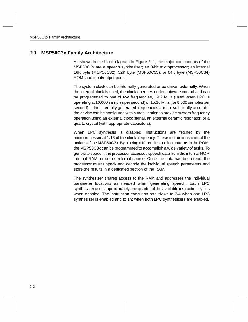
2 MSP50x3x Family Architecture 2-1. . . . . . . . . . . . . . . . . . . . . . . . . . . . . . . . . . . . . . . . . . . . . . . . . . . 2.1 MSP50C3x Family Architecture 2-2. . . . . . . . . . . . . . . . . . . . . . . . . . . . . . . . . . . . . . . . . . . . . . .
2.1.1 Read-Only Memory (ROM) 2-4. . . . . . . . . . . . . . . . . . . . . . . . . . . . . . . . . . . . . . . . . . . 2.1.2 Program Counter 2-5. . . . . . . . . . . . . . . . . . . . . . . . . . . . . . . . . . . . . . . . . . . . . . . . . . . . 2.1.3 Program Counter Stack 2-6. . . . . . . . . . . . . . . . . . . . . . . . . . . . . . . . . . . . . . . . . . . . . . 2.1.4 MSP50C3x Random Access Memory (RAM) 2-6. . . . . . . . . . . . . . . . . . . . . . . . . . . . 2.1.5 MSP50C3x Memory-Mapped Registers 2-9. . . . . . . . . . . . . . . . . . . . . . . . . . . . . . . . 2.1.6 Arithmetic Logic Unit (ALU) 2-11. . . . . . . . . . . . . . . . . . . . . . . . . . . . . . . . . . . . . . . . . . 2.1.7 A Register 2-11. . . . . . . . . . . . . . . . . . . . . . . . . . . . . . . . . . . . . . . . . . . . . . . . . . . . . . . . . 2.1.8 X Register 2-12. . . . . . . . . . . . . . . . . . . . . . . . . . . . . . . . . . . . . . . . . . . . . . . . . . . . . . . . . 2.1.9 B Register 2-12. . . . . . . . . . . . . . . . . . . . . . . . . . . . . . . . . . . . . . . . . . . . . . . . . . . . . . . . .
Running Title—Attribute Reference
x
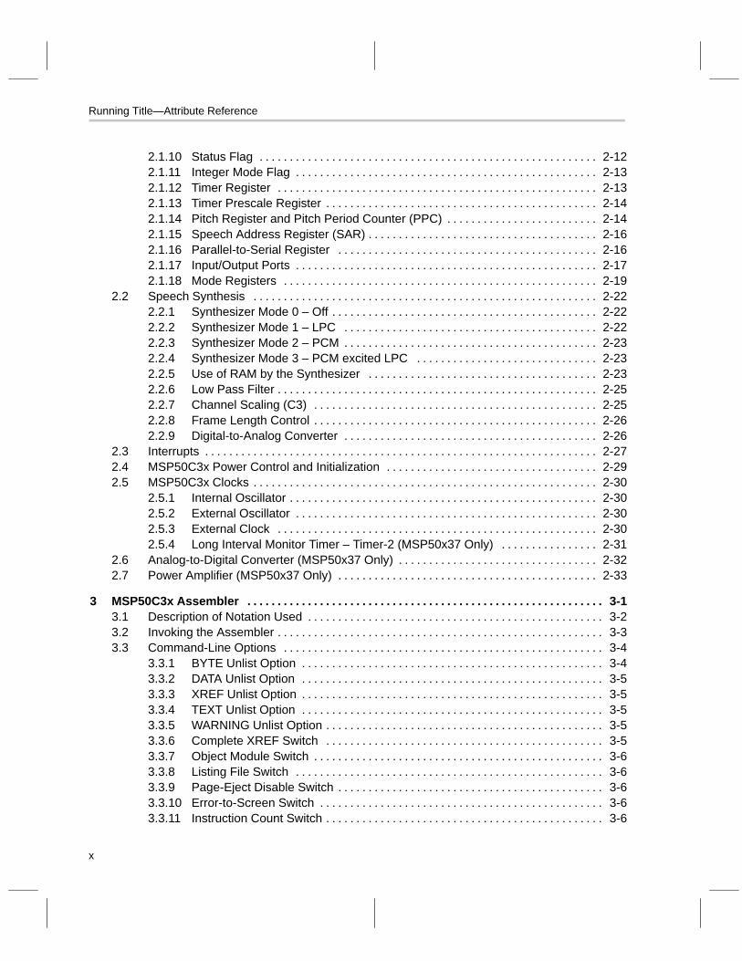
2.1.10 Status Flag 2-12. . . . . . . . . . . . . . . . . . . . . . . . . . . . . . . . . . . . . . . . . . . . . . . . . . . . . . . . 2.1.11 Integer Mode Flag 2-13. . . . . . . . . . . . . . . . . . . . . . . . . . . . . . . . . . . . . . . . . . . . . . . . . . 2.1.12 Timer Register 2-13. . . . . . . . . . . . . . . . . . . . . . . . . . . . . . . . . . . . . . . . . . . . . . . . . . . . . 2.1.13 Timer Prescale Register 2-14. . . . . . . . . . . . . . . . . . . . . . . . . . . . . . . . . . . . . . . . . . . . . 2.1.14 Pitch Register and Pitch Period Counter (PPC) 2-14. . . . . . . . . . . . . . . . . . . . . . . . . 2.1.15 Speech Address Register (SAR) 2-16. . . . . . . . . . . . . . . . . . . . . . . . . . . . . . . . . . . . . . 2.1.16 Parallel-to-Serial Register 2-16. . . . . . . . . . . . . . . . . . . . . . . . . . . . . . . . . . . . . . . . . . . 2.1.17 Input/Output Ports 2-17. . . . . . . . . . . . . . . . . . . . . . . . . . . . . . . . . . . . . . . . . . . . . . . . . . 2.1.18 Mode Registers 2-19. . . . . . . . . . . . . . . . . . . . . . . . . . . . . . . . . . . . . . . . . . . . . . . . . . . .
2.2 Speech Synthesis 2-22. . . . . . . . . . . . . . . . . . . . . . . . . . . . . . . . . . . . . . . . . . . . . . . . . . . . . . . . . 2.2.1 Synthesizer Mode 0 – Off 2-22. . . . . . . . . . . . . . . . . . . . . . . . . . . . . . . . . . . . . . . . . . . . 2.2.2 Synthesizer Mode 1 – LPC 2-22. . . . . . . . . . . . . . . . . . . . . . . . . . . . . . . . . . . . . . . . . . 2.2.3 Synthesizer Mode 2 – PCM 2-23. . . . . . . . . . . . . . . . . . . . . . . . . . . . . . . . . . . . . . . . . . 2.2.4 Synthesizer Mode 3 – PCM excited LPC 2-23. . . . . . . . . . . . . . . . . . . . . . . . . . . . . . 2.2.5 Use of RAM by the Synthesizer 2-23. . . . . . . . . . . . . . . . . . . . . . . . . . . . . . . . . . . . . . 2.2.6 Low Pass Filter 2-25. . . . . . . . . . . . . . . . . . . . . . . . . . . . . . . . . . . . . . . . . . . . . . . . . . . . . 2.2.7 Channel Scaling (C3) 2-25. . . . . . . . . . . . . . . . . . . . . . . . . . . . . . . . . . . . . . . . . . . . . . . 2.2.8 Frame Length Control 2-26. . . . . . . . . . . . . . . . . . . . . . . . . . . . . . . . . . . . . . . . . . . . . . . 2.2.9 Digital-to-Analog Converter 2-26. . . . . . . . . . . . . . . . . . . . . . . . . . . . . . . . . . . . . . . . . .
2.3 Interrupts 2-27. . . . . . . . . . . . . . . . . . . . . . . . . . . . . . . . . . . . . . . . . . . . . . . . . . . . . . . . . . . . . . . . . 2.4 MSP50C3x Power Control and Initialization 2-29. . . . . . . . . . . . . . . . . . . . . . . . . . . . . . . . . . . 2.5 MSP50C3x Clocks 2-30. . . . . . . . . . . . . . . . . . . . . . . . . . . . . . . . . . . . . . . . . . . . . . . . . . . . . . . . .
2.5.1 Internal Oscillator 2-30. . . . . . . . . . . . . . . . . . . . . . . . . . . . . . . . . . . . . . . . . . . . . . . . . . . 2.5.2 External Oscillator 2-30. . . . . . . . . . . . . . . . . . . . . . . . . . . . . . . . . . . . . . . . . . . . . . . . . . 2.5.3 External Clock 2-30. . . . . . . . . . . . . . . . . . . . . . . . . . . . . . . . . . . . . . . . . . . . . . . . . . . . . 2.5.4 Long Interval Monitor Timer – Timer-2 (MSP50x37 Only) 2-31. . . . . . . . . . . . . . . .
2.6 Analog-to-Digital Converter (MSP50x37 Only) 2-32. . . . . . . . . . . . . . . . . . . . . . . . . . . . . . . . . 2.7 Power Amplifier (MSP50x37 Only) 2-33. . . . . . . . . . . . . . . . . . . . . . . . . . . . . . . . . . . . . . . . . . .
3 MSP50C3x Assembler 3-1. . . . . . . . . . . . . . . . . . . . . . . . . . . . . . . . . . . . . . . . . . . . . . . . . . . . . . . . . . . 3.1 Description of Notation Used 3-2. . . . . . . . . . . . . . . . . . . . . . . . . . . . . . . . . . . . . . . . . . . . . . . . . 3.2 Invoking the Assembler 3-3. . . . . . . . . . . . . . . . . . . . . . . . . . . . . . . . . . . . . . . . . . . . . . . . . . . . . . 3.3 Command-Line Options 3-4. . . . . . . . . . . . . . . . . . . . . . . . . . . . . . . . . . . . . . . . . . . . . . . . . . . . .
3.3.1 BYTE Unlist Option 3-4. . . . . . . . . . . . . . . . . . . . . . . . . . . . . . . . . . . . . . . . . . . . . . . . . . 3.3.2 DATA Unlist Option 3-5. . . . . . . . . . . . . . . . . . . . . . . . . . . . . . . . . . . . . . . . . . . . . . . . . . 3.3.3 XREF Unlist Option 3-5. . . . . . . . . . . . . . . . . . . . . . . . . . . . . . . . . . . . . . . . . . . . . . . . . . 3.3.4 TEXT Unlist Option 3-5. . . . . . . . . . . . . . . . . . . . . . . . . . . . . . . . . . . . . . . . . . . . . . . . . . 3.3.5 WARNING Unlist Option 3-5. . . . . . . . . . . . . . . . . . . . . . . . . . . . . . . . . . . . . . . . . . . . . . 3.3.6 Complete XREF Switch 3-5. . . . . . . . . . . . . . . . . . . . . . . . . . . . . . . . . . . . . . . . . . . . . . 3.3.7 Object Module Switch 3-6. . . . . . . . . . . . . . . . . . . . . . . . . . . . . . . . . . . . . . . . . . . . . . . . 3.3.8 Listing File Switch 3-6. . . . . . . . . . . . . . . . . . . . . . . . . . . . . . . . . . . . . . . . . . . . . . . . . . . 3.3.9 Page-Eject Disable Switch 3-6. . . . . . . . . . . . . . . . . . . . . . . . . . . . . . . . . . . . . . . . . . . . 3.3.10 Error-to-Screen Switch 3-6. . . . . . . . . . . . . . . . . . . . . . . . . . . . . . . . . . . . . . . . . . . . . . . 3.3.11 Instruction Count Switch 3-6. . . . . . . . . . . . . . . . . . . . . . . . . . . . . . . . . . . . . . . . . . . . . .
Contents
xi Contents
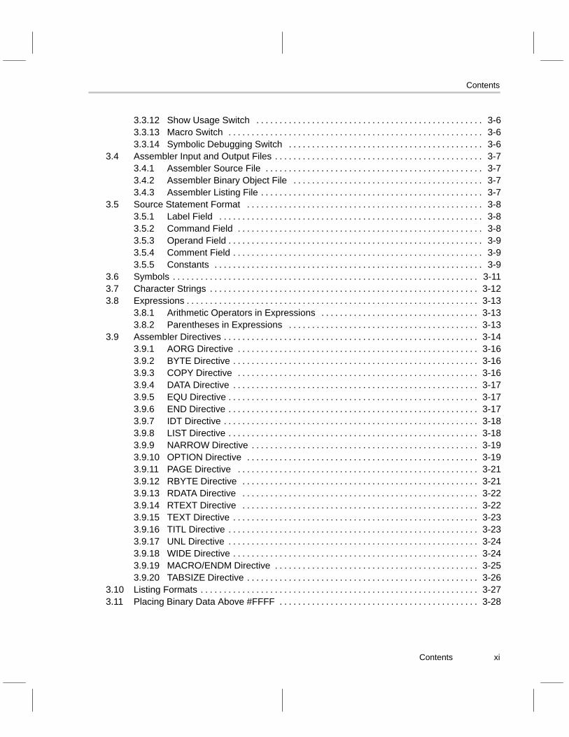
3.3.12 Show Usage Switch 3-6. . . . . . . . . . . . . . . . . . . . . . . . . . . . . . . . . . . . . . . . . . . . . . . . . 3.3.13 Macro Switch 3-6. . . . . . . . . . . . . . . . . . . . . . . . . . . . . . . . . . . . . . . . . . . . . . . . . . . . . . . 3.3.14 Symbolic Debugging Switch 3-6. . . . . . . . . . . . . . . . . . . . . . . . . . . . . . . . . . . . . . . . . .
3.4 Assembler Input and Output Files 3-7. . . . . . . . . . . . . . . . . . . . . . . . . . . . . . . . . . . . . . . . . . . . . 3.4.1 Assembler Source File 3-7. . . . . . . . . . . . . . . . . . . . . . . . . . . . . . . . . . . . . . . . . . . . . . . 3.4.2 Assembler Binary Object File 3-7. . . . . . . . . . . . . . . . . . . . . . . . . . . . . . . . . . . . . . . . . 3.4.3 Assembler Listing File 3-7. . . . . . . . . . . . . . . . . . . . . . . . . . . . . . . . . . . . . . . . . . . . . . . .
3.5 Source Statement Format 3-8. . . . . . . . . . . . . . . . . . . . . . . . . . . . . . . . . . . . . . . . . . . . . . . . . . . 3.5.1 Label Field 3-8. . . . . . . . . . . . . . . . . . . . . . . . . . . . . . . . . . . . . . . . . . . . . . . . . . . . . . . . . 3.5.2 Command Field 3-8. . . . . . . . . . . . . . . . . . . . . . . . . . . . . . . . . . . . . . . . . . . . . . . . . . . . . 3.5.3 Operand Field 3-9. . . . . . . . . . . . . . . . . . . . . . . . . . . . . . . . . . . . . . . . . . . . . . . . . . . . . . . 3.5.4 Comment Field 3-9. . . . . . . . . . . . . . . . . . . . . . . . . . . . . . . . . . . . . . . . . . . . . . . . . . . . . . 3.5.5 Constants 3-9. . . . . . . . . . . . . . . . . . . . . . . . . . . . . . . . . . . . . . . . . . . . . . . . . . . . . . . . . .
3.6 Symbols 3-11. . . . . . . . . . . . . . . . . . . . . . . . . . . . . . . . . . . . . . . . . . . . . . . . . . . . . . . . . . . . . . . . . . 3.7 Character Strings 3-12. . . . . . . . . . . . . . . . . . . . . . . . . . . . . . . . . . . . . . . . . . . . . . . . . . . . . . . . . . 3.8 Expressions 3-13. . . . . . . . . . . . . . . . . . . . . . . . . . . . . . . . . . . . . . . . . . . . . . . . . . . . . . . . . . . . . . .
3.8.1 Arithmetic Operators in Expressions 3-13. . . . . . . . . . . . . . . . . . . . . . . . . . . . . . . . . . 3.8.2 Parentheses in Expressions 3-13. . . . . . . . . . . . . . . . . . . . . . . . . . . . . . . . . . . . . . . . .
3.9 Assembler Directives 3-14. . . . . . . . . . . . . . . . . . . . . . . . . . . . . . . . . . . . . . . . . . . . . . . . . . . . . . . 3.9.1 AORG Directive 3-16. . . . . . . . . . . . . . . . . . . . . . . . . . . . . . . . . . . . . . . . . . . . . . . . . . . . 3.9.2 BYTE Directive 3-16. . . . . . . . . . . . . . . . . . . . . . . . . . . . . . . . . . . . . . . . . . . . . . . . . . . . . 3.9.3 COPY Directive 3-16. . . . . . . . . . . . . . . . . . . . . . . . . . . . . . . . . . . . . . . . . . . . . . . . . . . . 3.9.4 DATA Directive 3-17. . . . . . . . . . . . . . . . . . . . . . . . . . . . . . . . . . . . . . . . . . . . . . . . . . . . . 3.9.5 EQU Directive 3-17. . . . . . . . . . . . . . . . . . . . . . . . . . . . . . . . . . . . . . . . . . . . . . . . . . . . . . 3.9.6 END Directive 3-17. . . . . . . . . . . . . . . . . . . . . . . . . . . . . . . . . . . . . . . . . . . . . . . . . . . . . . 3.9.7 IDT Directive 3-18. . . . . . . . . . . . . . . . . . . . . . . . . . . . . . . . . . . . . . . . . . . . . . . . . . . . . . . 3.9.8 LIST Directive 3-18. . . . . . . . . . . . . . . . . . . . . . . . . . . . . . . . . . . . . . . . . . . . . . . . . . . . . . 3.9.9 NARROW Directive 3-19. . . . . . . . . . . . . . . . . . . . . . . . . . . . . . . . . . . . . . . . . . . . . . . . . 3.9.10 OPTION Directive 3-19. . . . . . . . . . . . . . . . . . . . . . . . . . . . . . . . . . . . . . . . . . . . . . . . . . 3.9.11 PAGE Directive 3-21. . . . . . . . . . . . . . . . . . . . . . . . . . . . . . . . . . . . . . . . . . . . . . . . . . . . 3.9.12 RBYTE Directive 3-21. . . . . . . . . . . . . . . . . . . . . . . . . . . . . . . . . . . . . . . . . . . . . . . . . . . 3.9.13 RDATA Directive 3-22. . . . . . . . . . . . . . . . . . . . . . . . . . . . . . . . . . . . . . . . . . . . . . . . . . . 3.9.14 RTEXT Directive 3-22. . . . . . . . . . . . . . . . . . . . . . . . . . . . . . . . . . . . . . . . . . . . . . . . . . . 3.9.15 TEXT Directive 3-23. . . . . . . . . . . . . . . . . . . . . . . . . . . . . . . . . . . . . . . . . . . . . . . . . . . . . 3.9.16 TITL Directive 3-23. . . . . . . . . . . . . . . . . . . . . . . . . . . . . . . . . . . . . . . . . . . . . . . . . . . . . . 3.9.17 UNL Directive 3-24. . . . . . . . . . . . . . . . . . . . . . . . . . . . . . . . . . . . . . . . . . . . . . . . . . . . . . 3.9.18 WIDE Directive 3-24. . . . . . . . . . . . . . . . . . . . . . . . . . . . . . . . . . . . . . . . . . . . . . . . . . . . . 3.9.19 MACRO/ENDM Directive 3-25. . . . . . . . . . . . . . . . . . . . . . . . . . . . . . . . . . . . . . . . . . . . 3.9.20 TABSIZE Directive 3-26. . . . . . . . . . . . . . . . . . . . . . . . . . . . . . . . . . . . . . . . . . . . . . . . . .
3.10 Listing Formats 3-27. . . . . . . . . . . . . . . . . . . . . . . . . . . . . . . . . . . . . . . . . . . . . . . . . . . . . . . . . . . . 3.11 Placing Binary Data Above #FFFF 3-28. . . . . . . . . . . . . . . . . . . . . . . . . . . . . . . . . . . . . . . . . . .
Contents
xii
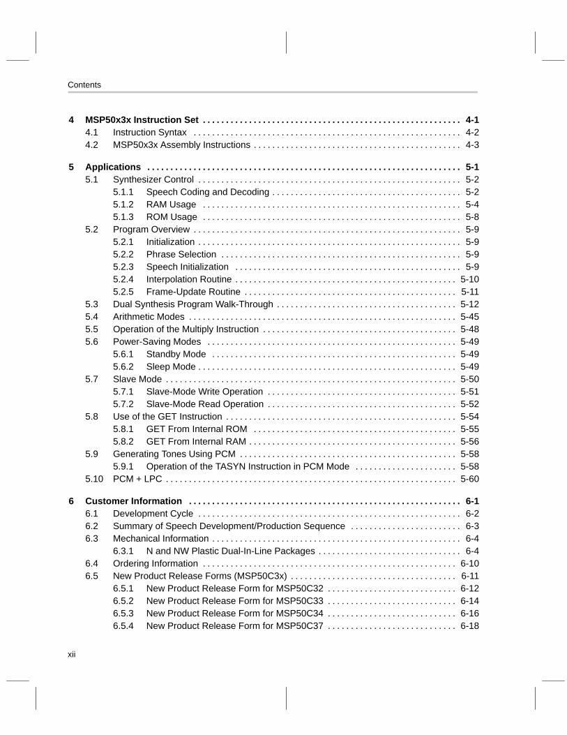
4 MSP50x3x Instruction Set 4-1. . . . . . . . . . . . . . . . . . . . . . . . . . . . . . . . . . . . . . . . . . . . . . . . . . . . . . . . 4.1 Instruction Syntax 4-2. . . . . . . . . . . . . . . . . . . . . . . . . . . . . . . . . . . . . . . . . . . . . . . . . . . . . . . . . . 4.2 MSP50x3x Assembly Instructions 4-3. . . . . . . . . . . . . . . . . . . . . . . . . . . . . . . . . . . . . . . . . . . . .
5 Applications 5-1. . . . . . . . . . . . . . . . . . . . . . . . . . . . . . . . . . . . . . . . . . . . . . . . . . . . . . . . . . . . . . . . . . . . 5.1 Synthesizer Control 5-2. . . . . . . . . . . . . . . . . . . . . . . . . . . . . . . . . . . . . . . . . . . . . . . . . . . . . . . . .
5.1.1 Speech Coding and Decoding 5-2. . . . . . . . . . . . . . . . . . . . . . . . . . . . . . . . . . . . . . . . . 5.1.2 RAM Usage 5-4. . . . . . . . . . . . . . . . . . . . . . . . . . . . . . . . . . . . . . . . . . . . . . . . . . . . . . . . 5.1.3 ROM Usage 5-8. . . . . . . . . . . . . . . . . . . . . . . . . . . . . . . . . . . . . . . . . . . . . . . . . . . . . . . .
5.2 Program Overview 5-9. . . . . . . . . . . . . . . . . . . . . . . . . . . . . . . . . . . . . . . . . . . . . . . . . . . . . . . . . . 5.2.1 Initialization 5-9. . . . . . . . . . . . . . . . . . . . . . . . . . . . . . . . . . . . . . . . . . . . . . . . . . . . . . . . . 5.2.2 Phrase Selection 5-9. . . . . . . . . . . . . . . . . . . . . . . . . . . . . . . . . . . . . . . . . . . . . . . . . . . . 5.2.3 Speech Initialization 5-9. . . . . . . . . . . . . . . . . . . . . . . . . . . . . . . . . . . . . . . . . . . . . . . . . 5.2.4 Interpolation Routine 5-10. . . . . . . . . . . . . . . . . . . . . . . . . . . . . . . . . . . . . . . . . . . . . . . . 5.2.5 Frame-Update Routine 5-11. . . . . . . . . . . . . . . . . . . . . . . . . . . . . . . . . . . . . . . . . . . . . .
5.3 Dual Synthesis Program Walk-Through 5-12. . . . . . . . . . . . . . . . . . . . . . . . . . . . . . . . . . . . . . . 5.4 Arithmetic Modes 5-45. . . . . . . . . . . . . . . . . . . . . . . . . . . . . . . . . . . . . . . . . . . . . . . . . . . . . . . . . . 5.5 Operation of the Multiply Instruction 5-48. . . . . . . . . . . . . . . . . . . . . . . . . . . . . . . . . . . . . . . . . . 5.6 Power-Saving Modes 5-49. . . . . . . . . . . . . . . . . . . . . . . . . . . . . . . . . . . . . . . . . . . . . . . . . . . . . .
5.6.1 Standby Mode 5-49. . . . . . . . . . . . . . . . . . . . . . . . . . . . . . . . . . . . . . . . . . . . . . . . . . . . . 5.6.2 Sleep Mode 5-49. . . . . . . . . . . . . . . . . . . . . . . . . . . . . . . . . . . . . . . . . . . . . . . . . . . . . . . .
5.7 Slave Mode 5-50. . . . . . . . . . . . . . . . . . . . . . . . . . . . . . . . . . . . . . . . . . . . . . . . . . . . . . . . . . . . . . . 5.7.1 Slave-Mode Write Operation 5-51. . . . . . . . . . . . . . . . . . . . . . . . . . . . . . . . . . . . . . . . . 5.7.2 Slave-Mode Read Operation 5-52. . . . . . . . . . . . . . . . . . . . . . . . . . . . . . . . . . . . . . . . .
5.8 Use of the GET Instruction 5-54. . . . . . . . . . . . . . . . . . . . . . . . . . . . . . . . . . . . . . . . . . . . . . . . . . 5.8.1 GET From Internal ROM 5-55. . . . . . . . . . . . . . . . . . . . . . . . . . . . . . . . . . . . . . . . . . . . 5.8.2 GET From Internal RAM 5-56. . . . . . . . . . . . . . . . . . . . . . . . . . . . . . . . . . . . . . . . . . . . .
5.9 Generating Tones Using PCM 5-58. . . . . . . . . . . . . . . . . . . . . . . . . . . . . . . . . . . . . . . . . . . . . . . 5.9.1 Operation of the TASYN Instruction in PCM Mode 5-58. . . . . . . . . . . . . . . . . . . . . .
5.10 PCM + LPC 5-60. . . . . . . . . . . . . . . . . . . . . . . . . . . . . . . . . . . . . . . . . . . . . . . . . . . . . . . . . . . . . . .
6 Customer Information 6-1. . . . . . . . . . . . . . . . . . . . . . . . . . . . . . . . . . . . . . . . . . . . . . . . . . . . . . . . . . . 6.1 Development Cycle 6-2. . . . . . . . . . . . . . . . . . . . . . . . . . . . . . . . . . . . . . . . . . . . . . . . . . . . . . . . . 6.2 Summary of Speech Development/Production Sequence 6-3. . . . . . . . . . . . . . . . . . . . . . . . 6.3 Mechanical Information 6-4. . . . . . . . . . . . . . . . . . . . . . . . . . . . . . . . . . . . . . . . . . . . . . . . . . . . . .
6.3.1 N and NW Plastic Dual-In-Line Packages 6-4. . . . . . . . . . . . . . . . . . . . . . . . . . . . . . . 6.4 Ordering Information 6-10. . . . . . . . . . . . . . . . . . . . . . . . . . . . . . . . . . . . . . . . . . . . . . . . . . . . . . . 6.5 New Product Release Forms (MSP50C3x) 6-11. . . . . . . . . . . . . . . . . . . . . . . . . . . . . . . . . . . .
6.5.1 New Product Release Form for MSP50C32 6-12. . . . . . . . . . . . . . . . . . . . . . . . . . . . 6.5.2 New Product Release Form for MSP50C33 6-14. . . . . . . . . . . . . . . . . . . . . . . . . . . . 6.5.3 New Product Release Form for MSP50C34 6-16. . . . . . . . . . . . . . . . . . . . . . . . . . . . 6.5.4 New Product Release Form for MSP50C37 6-18. . . . . . . . . . . . . . . . . . . . . . . . . . . .
Contents
xiii Contents
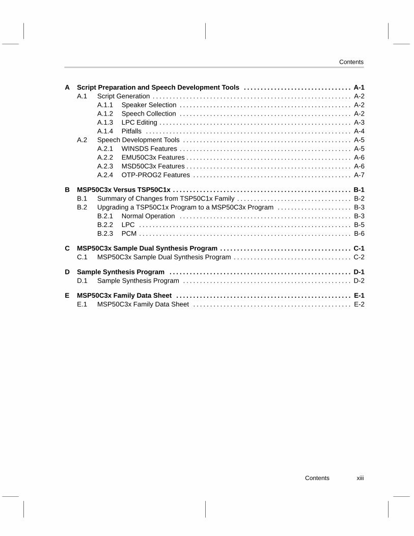
A Script Preparation and Speech Development Tools A-1. . . . . . . . . . . . . . . . . . . . . . . . . . . . . . . . A.1 Script Generation A-2. . . . . . . . . . . . . . . . . . . . . . . . . . . . . . . . . . . . . . . . . . . . . . . . . . . . . . . . . . .
A.1.1 Speaker Selection A-2. . . . . . . . . . . . . . . . . . . . . . . . . . . . . . . . . . . . . . . . . . . . . . . . . . . A.1.2 Speech Collection A-2. . . . . . . . . . . . . . . . . . . . . . . . . . . . . . . . . . . . . . . . . . . . . . . . . . . A.1.3 LPC Editing A-3. . . . . . . . . . . . . . . . . . . . . . . . . . . . . . . . . . . . . . . . . . . . . . . . . . . . . . . . . A.1.4 Pitfalls A-4. . . . . . . . . . . . . . . . . . . . . . . . . . . . . . . . . . . . . . . . . . . . . . . . . . . . . . . . . . . . .
A.2 Speech Development Tools A-5. . . . . . . . . . . . . . . . . . . . . . . . . . . . . . . . . . . . . . . . . . . . . . . . . . A.2.1 WINSDS Features A-5. . . . . . . . . . . . . . . . . . . . . . . . . . . . . . . . . . . . . . . . . . . . . . . . . . . A.2.2 EMU50C3x Features A-6. . . . . . . . . . . . . . . . . . . . . . . . . . . . . . . . . . . . . . . . . . . . . . . . . A.2.3 MSD50C3x Features A-6. . . . . . . . . . . . . . . . . . . . . . . . . . . . . . . . . . . . . . . . . . . . . . . . . A.2.4 OTP-PROG2 Features A-7. . . . . . . . . . . . . . . . . . . . . . . . . . . . . . . . . . . . . . . . . . . . . . .
B MSP50C3x Versus TSP50C1x B-1. . . . . . . . . . . . . . . . . . . . . . . . . . . . . . . . . . . . . . . . . . . . . . . . . . . . . B.1 Summary of Changes from TSP50C1x Family B-2. . . . . . . . . . . . . . . . . . . . . . . . . . . . . . . . . . B.2 Upgrading a TSP50C1x Program to a MSP50C3x Program B-3. . . . . . . . . . . . . . . . . . . . . .
B.2.1 Normal Operation B-3. . . . . . . . . . . . . . . . . . . . . . . . . . . . . . . . . . . . . . . . . . . . . . . . . . . B.2.2 LPC B-5. . . . . . . . . . . . . . . . . . . . . . . . . . . . . . . . . . . . . . . . . . . . . . . . . . . . . . . . . . . . . . . B.2.3 PCM B-6. . . . . . . . . . . . . . . . . . . . . . . . . . . . . . . . . . . . . . . . . . . . . . . . . . . . . . . . . . . . . . .
C MSP50C3x Sample Dual Synthesis Program C-1. . . . . . . . . . . . . . . . . . . . . . . . . . . . . . . . . . . . . . . C.1 MSP50C3x Sample Dual Synthesis Program C-2. . . . . . . . . . . . . . . . . . . . . . . . . . . . . . . . . . .
D Sample Synthesis Program D-1. . . . . . . . . . . . . . . . . . . . . . . . . . . . . . . . . . . . . . . . . . . . . . . . . . . . . . D.1 Sample Synthesis Program D-2. . . . . . . . . . . . . . . . . . . . . . . . . . . . . . . . . . . . . . . . . . . . . . . . . .
E MSP50C3x Family Data Sheet E-1. . . . . . . . . . . . . . . . . . . . . . . . . . . . . . . . . . . . . . . . . . . . . . . . . . . . E.1 MSP50C3x Family Data Sheet E-2. . . . . . . . . . . . . . . . . . . . . . . . . . . . . . . . . . . . . . . . . . . . . . .
Figures
xiv
Figures
1–1 MSP50x3x Functional Block Diagram 1-4. . . . . . . . . . . . . . . . . . . . . . . . . . . . . . . . . . . . . . . . . . . . 1–2 MSP50x37 Functional Block Diagram 1-5. . . . . . . . . . . . . . . . . . . . . . . . . . . . . . . . . . . . . . . . . . . . 1–3 D/A Output Waveforms for Two-Pin Push Pull (Option 1) 1-9. . . . . . . . . . . . . . . . . . . . . . . . . . . 1–4 Four-Transistor Amplifier Circuit 1-10. . . . . . . . . . . . . . . . . . . . . . . . . . . . . . . . . . . . . . . . . . . . . . . . 1–5 Operational Amplifier Interface Circuit 1-10. . . . . . . . . . . . . . . . . . . . . . . . . . . . . . . . . . . . . . . . . . . 1–6 Power Amplifier Interface Circuit 1-11. . . . . . . . . . . . . . . . . . . . . . . . . . . . . . . . . . . . . . . . . . . . . . . 1–7 Figure 1–7. D/A Output Waveforms for Single-Pin Double-Ended (Option 2) 1-12. . . . . . . . . 1–8 Operational Amplifier Interface Circuit 1-13. . . . . . . . . . . . . . . . . . . . . . . . . . . . . . . . . . . . . . . . . . . 1–9 Two-Pin Push Pull Power Amplifier Output Circuit with External LPF 1-14. . . . . . . . . . . . . . . . 1–10 One-Pin Analog Power Amplifier Output Circuit with External LPF 1-14. . . . . . . . . . . . . . . . . . 1–11 MSP50x32/33/34 16-Pin Package Terminal Assignments 1-15. . . . . . . . . . . . . . . . . . . . . . . . . . 1–12 Power-Up Initialization Circuit 1-17. . . . . . . . . . . . . . . . . . . . . . . . . . . . . . . . . . . . . . . . . . . . . . . . . . 1–13 MSP50P34 40-Pin Package Terminal Assignments 1-18. . . . . . . . . . . . . . . . . . . . . . . . . . . . . . . 1–14 MSP50x37 28-Pin Package Terminal Assignments 1-21. . . . . . . . . . . . . . . . . . . . . . . . . . . . . . . 1–15 LPC-12 Vocal Tract Model 1-24. . . . . . . . . . . . . . . . . . . . . . . . . . . . . . . . . . . . . . . . . . . . . . . . . . . . . 1–16 Oscillator Circuit 1-26. . . . . . . . . . . . . . . . . . . . . . . . . . . . . . . . . . . . . . . . . . . . . . . . . . . . . . . . . . . . . 1–17 External Clock Interface 1-26. . . . . . . . . . . . . . . . . . . . . . . . . . . . . . . . . . . . . . . . . . . . . . . . . . . . . . . 2–1 MSP50C3x System Block Diagram 2-3. . . . . . . . . . . . . . . . . . . . . . . . . . . . . . . . . . . . . . . . . . . . . . 2–2 MSP50x37 System Block Diagram 2-4. . . . . . . . . . . . . . . . . . . . . . . . . . . . . . . . . . . . . . . . . . . . . . 2–3 MSP50x32/33/34 RAM Map 2-7. . . . . . . . . . . . . . . . . . . . . . . . . . . . . . . . . . . . . . . . . . . . . . . . . . . . 2–4 MSP50x37 RAM Map 2-8. . . . . . . . . . . . . . . . . . . . . . . . . . . . . . . . . . . . . . . . . . . . . . . . . . . . . . . . . . 2–5 RAM Map During Speech Generation 2-24. . . . . . . . . . . . . . . . . . . . . . . . . . . . . . . . . . . . . . . . . . . 2–6 Oversampling Output Filter 2-25. . . . . . . . . . . . . . . . . . . . . . . . . . . . . . . . . . . . . . . . . . . . . . . . . . . . 2–7 Oversampling Output Filter Circuit 2-33. . . . . . . . . . . . . . . . . . . . . . . . . . . . . . . . . . . . . . . . . . . . . . 5–1 D6 Frame Decoding 5-3. . . . . . . . . . . . . . . . . . . . . . . . . . . . . . . . . . . . . . . . . . . . . . . . . . . . . . . . . . . 5–2 Speech Parameter Unpacking and Decoding 5-4. . . . . . . . . . . . . . . . . . . . . . . . . . . . . . . . . . . . . 5–3 ACAAC in Extended-Sign Mode 5-47. . . . . . . . . . . . . . . . . . . . . . . . . . . . . . . . . . . . . . . . . . . . . . . . 5–4 ACAAC in Integer Mode 5-47. . . . . . . . . . . . . . . . . . . . . . . . . . . . . . . . . . . . . . . . . . . . . . . . . . . . . . 5–5 Slave-Mode Write Operation 5-52. . . . . . . . . . . . . . . . . . . . . . . . . . . . . . . . . . . . . . . . . . . . . . . . . . . 5–6 Slave-Mode Read-Then-Write Operation 5-53. . . . . . . . . . . . . . . . . . . . . . . . . . . . . . . . . . . . . . . . 5–7 Register Connections for GET Instruction 5-54. . . . . . . . . . . . . . . . . . . . . . . . . . . . . . . . . . . . . . . 5–8 Parallel-to-Serial Operation for GET 5 Instruction 5-55. . . . . . . . . . . . . . . . . . . . . . . . . . . . . . . . . 5–9 Operation of TASYN in PCM Mode 5-58. . . . . . . . . . . . . . . . . . . . . . . . . . . . . . . . . . . . . . . . . . . . . 5–10 Format of Data in A Register before TASYN 5-58. . . . . . . . . . . . . . . . . . . . . . . . . . . . . . . . . . . . . 6–1 Speech Development Cycle 6-2. . . . . . . . . . . . . . . . . . . . . . . . . . . . . . . . . . . . . . . . . . . . . . . . . . . . 6–2 MSP50C32/33/34 16-Pin N Package 6-5. . . . . . . . . . . . . . . . . . . . . . . . . . . . . . . . . . . . . . . . . . . .
Figures
xv Contents
6–3 MSP50C32/33/34 28-Pin N Package 6-6. . . . . . . . . . . . . . . . . . . . . . . . . . . . . . . . . . . . . . . . . . . . 6–4 MSP50P34 40-Pin NW Package 6-7. . . . . . . . . . . . . . . . . . . . . . . . . . . . . . . . . . . . . . . . . . . . . . . . 6–5 MSP50C32/33/34 and MSP50P34/37 DW Package 6-9. . . . . . . . . . . . . . . . . . . . . . . . . . . . . . . A–1 WINSDS A-5. . . . . . . . . . . . . . . . . . . . . . . . . . . . . . . . . . . . . . . . . . . . . . . . . . . . . . . . . . . . . . . . . . . . . A–2 EMU50C3x A-6. . . . . . . . . . . . . . . . . . . . . . . . . . . . . . . . . . . . . . . . . . . . . . . . . . . . . . . . . . . . . . . . . . . A–3 MSD50C3x A-6. . . . . . . . . . . . . . . . . . . . . . . . . . . . . . . . . . . . . . . . . . . . . . . . . . . . . . . . . . . . . . . . . . . A–4 OTP-PROG A-7. . . . . . . . . . . . . . . . . . . . . . . . . . . . . . . . . . . . . . . . . . . . . . . . . . . . . . . . . . . . . . . . . .
Tables
xvi
Tables
1–1 MSP50x3x Device Family 1-2. . . . . . . . . . . . . . . . . . . . . . . . . . . . . . . . . . . . . . . . . . . . . . . . . . . . . . 1–2 MSP50x3x D/A Options 1-8. . . . . . . . . . . . . . . . . . . . . . . . . . . . . . . . . . . . . . . . . . . . . . . . . . . . . . . . 1–3 MSP50C32/33/34 16-Pin Package Terminal Functions 1-16. . . . . . . . . . . . . . . . . . . . . . . . . . . . 1–4 Pad Location on the MSP50C32/C33 Die Form 1-17. . . . . . . . . . . . . . . . . . . . . . . . . . . . . . . . . . 1–5 MSP50P34 40-Pin Package Terminal Functions 1-19. . . . . . . . . . . . . . . . . . . . . . . . . . . . . . . . . . 1–6 Pad Location on the MSP50C34/P34 Die Form 1-20. . . . . . . . . . . . . . . . . . . . . . . . . . . . . . . . . . 1–7 MSP50x37 28-Pin Package Terminal Functions 1-22. . . . . . . . . . . . . . . . . . . . . . . . . . . . . . . . . . 2–1 Reserved ROM Locations 2-5. . . . . . . . . . . . . . . . . . . . . . . . . . . . . . . . . . . . . . . . . . . . . . . . . . . . . . 2–2 Memory-Mapped Registers 2-10. . . . . . . . . . . . . . . . . . . . . . . . . . . . . . . . . . . . . . . . . . . . . . . . . . . . 2–3 I/O Registers 2-17. . . . . . . . . . . . . . . . . . . . . . . . . . . . . . . . . . . . . . . . . . . . . . . . . . . . . . . . . . . . . . . . 2–4 I/O Terminal Functions 2-17. . . . . . . . . . . . . . . . . . . . . . . . . . . . . . . . . . . . . . . . . . . . . . . . . . . . . . . . 2–5 Mode Register 1 2-20. . . . . . . . . . . . . . . . . . . . . . . . . . . . . . . . . . . . . . . . . . . . . . . . . . . . . . . . . . . . . 2–6 Mode Register 2 2-21. . . . . . . . . . . . . . . . . . . . . . . . . . . . . . . . . . . . . . . . . . . . . . . . . . . . . . . . . . . . . 2–7 Level-1 Interrupt Vectors 2-27. . . . . . . . . . . . . . . . . . . . . . . . . . . . . . . . . . . . . . . . . . . . . . . . . . . . . . 2–8 Level-2 Interrupt Vectors 2-27. . . . . . . . . . . . . . . . . . . . . . . . . . . . . . . . . . . . . . . . . . . . . . . . . . . . . . 2–9 Memory Assignment for Additional Timer 2-31. . . . . . . . . . . . . . . . . . . . . . . . . . . . . . . . . . . . . . . . 2–10 D Port Terminal MUX of ADC input for RAM 2-32. . . . . . . . . . . . . . . . . . . . . . . . . . . . . . . . . . . . . 3–1 Switches and Options 3-4. . . . . . . . . . . . . . . . . . . . . . . . . . . . . . . . . . . . . . . . . . . . . . . . . . . . . . . . . 3–2 Summary of Assembler Directives 3-15. . . . . . . . . . . . . . . . . . . . . . . . . . . . . . . . . . . . . . . . . . . . . . 4–1 MSP50x3x Instruction Set 4-3. . . . . . . . . . . . . . . . . . . . . . . . . . . . . . . . . . . . . . . . . . . . . . . . . . . . . . 4–2 MSP50x3x Instruction Table 4-6. . . . . . . . . . . . . . . . . . . . . . . . . . . . . . . . . . . . . . . . . . . . . . . . . . . . 5–1 D6 Parameter Size 5-2. . . . . . . . . . . . . . . . . . . . . . . . . . . . . . . . . . . . . . . . . . . . . . . . . . . . . . . . . . . . 5–2 Hardware-Fixed RAM Locations 5-5. . . . . . . . . . . . . . . . . . . . . . . . . . . . . . . . . . . . . . . . . . . . . . . . 5–3 Other RAM Locations Used in Sample Program 5-6. . . . . . . . . . . . . . . . . . . . . . . . . . . . . . . . . . . 5–4 FLAGS Bit Descriptions for Sample Program 5-8. . . . . . . . . . . . . . . . . . . . . . . . . . . . . . . . . . . . . 5–5 FLAGS_1 and FLAGS_2 Bit Descriptions for Sample Program 5-8. . . . . . . . . . . . . . . . . . . . . . 5–6 ROM Usage 5-8. . . . . . . . . . . . . . . . . . . . . . . . . . . . . . . . . . . . . . . . . . . . . . . . . . . . . . . . . . . . . . . . . . 5–7 TXA Operation 5-46. . . . . . . . . . . . . . . . . . . . . . . . . . . . . . . . . . . . . . . . . . . . . . . . . . . . . . . . . . . . . . . 5–8 Mode Register Control of GET Data Source 5-55. . . . . . . . . . . . . . . . . . . . . . . . . . . . . . . . . . . . . 5–9 Relative Weights of DAC Magnitude Bits 5-59. . . . . . . . . . . . . . . . . . . . . . . . . . . . . . . . . . . . . . . . B–1 Interrupt Vectors for the TSP50C1x and the MSP50C3x B-3. . . . . . . . . . . . . . . . . . . . . . . . . . . . B–2 I/O Ports for the TSP50C1x and the MSP50C3x B-4. . . . . . . . . . . . . . . . . . . . . . . . . . . . . . . . . . .
Examples
xvii Contents
Examples
3–1 XREF Unlist Option 3-5. . . . . . . . . . . . . . . . . . . . . . . . . . . . . . . . . . . . . . . . . . . . . . . . . . . . . . . . . . .
Notes, Cautions, and Warnings
xviii
Notes and Cautions
MSP50C34I/O Lines 1-15. . . . . . . . . . . . . . . . . . . . . . . . . . . . . . . . . . . . . . . . . . . . . . . . . . . . . . . . . . . . . . . . . Unused I/O Terminals 2-18. . . . . . . . . . . . . . . . . . . . . . . . . . . . . . . . . . . . . . . . . . . . . . . . . . . . . . . . . . . . . . . . 24 I/O Pins 2-18. . . . . . . . . . . . . . . . . . . . . . . . . . . . . . . . . . . . . . . . . . . . . . . . . . . . . . . . . . . . . . . . . . . . . . . . . Using the ORCM Instruction 2-19. . . . . . . . . . . . . . . . . . . . . . . . . . . . . . . . . . . . . . . . . . . . . . . . . . . . . . . . . . TSP50C1x Device Family 2-29. . . . . . . . . . . . . . . . . . . . . . . . . . . . . . . . . . . . . . . . . . . . . . . . . . . . . . . . . . . . Additional Precautions 2-29. . . . . . . . . . . . . . . . . . . . . . . . . . . . . . . . . . . . . . . . . . . . . . . . . . . . . . . . . . . . . . . Long Interval Timer 2-31. . . . . . . . . . . . . . . . . . . . . . . . . . . . . . . . . . . . . . . . . . . . . . . . . . . . . . . . . . . . . . . . . . Transferring Data to the A Register 2-31. . . . . . . . . . . . . . . . . . . . . . . . . . . . . . . . . . . . . . . . . . . . . . . . . . . . MSP50x37 Timer Registers and the Development Tools 2-31. . . . . . . . . . . . . . . . . . . . . . . . . . . . . . . . . . AORG# 10000 Statement Restriction 3-28. . . . . . . . . . . . . . . . . . . . . . . . . . . . . . . . . . . . . . . . . . . . . . . . . . Extended-Sign Mode 4-32. . . . . . . . . . . . . . . . . . . . . . . . . . . . . . . . . . . . . . . . . . . . . . . . . . . . . . . . . . . . . . . . Extended-Sign Mode 4-33. . . . . . . . . . . . . . . . . . . . . . . . . . . . . . . . . . . . . . . . . . . . . . . . . . . . . . . . . . . . . . . . RETI Executed With Interrupts Enabled 4-36. . . . . . . . . . . . . . . . . . . . . . . . . . . . . . . . . . . . . . . . . . . . . . . . GET Instruction 5-55. . . . . . . . . . . . . . . . . . . . . . . . . . . . . . . . . . . . . . . . . . . . . . . . . . . . . . . . . . . . . . . . . . . . . Using Prototype Devices in Production Systems 6-3. . . . . . . . . . . . . . . . . . . . . . . . . . . . . . . . . . . . . . . . . . Required and Recommended Equipment A-5. . . . . . . . . . . . . . . . . . . . . . . . . . . . . . . . . . . . . . . . . . . . . . . . TSP50C19 B-5. . . . . . . . . . . . . . . . . . . . . . . . . . . . . . . . . . . . . . . . . . . . . . . . . . . . . . . . . . . . . . . . . . . . . . . . . .
1-1
Introduction to The MSP50x3x Family
The MSP50x3x family uses a revolutionary architecture to combine an 8-bitmicroprocessor, two speech synthesizers, ROM, RAM, and I/O in a low-costsingle-chip system. The architecture uses the same arithmetic logic unit (ALU)for the two synthesizers and the microprocessor, thus reducing chip area andcost and enabling the microprocessor to do a multiply operation in 0.8 µs. TheMSP50x3x family features two semi-independent channels of linear predictivecoding (LPC), which synthesize high-quality speech at a low data rate. Pulse-code modulation (PCM) can produce music or sound effects. LPC and PCMcan be added together to produce a composite result.
Topic Page
1.1 MSP50x3x Device Family 1-2. . . . . . . . . . . . . . . . . . . . . . . . . . . . . . . . . . . . . .
1.2 Applications 1-3. . . . . . . . . . . . . . . . . . . . . . . . . . . . . . . . . . . . . . . . . . . . . . . . . .
1.3 Description 1-4. . . . . . . . . . . . . . . . . . . . . . . . . . . . . . . . . . . . . . . . . . . . . . . . . . .
1.4 Features 1-6. . . . . . . . . . . . . . . . . . . . . . . . . . . . . . . . . . . . . . . . . . . . . . . . . . . . .
1.5 D/A Options 1-8. . . . . . . . . . . . . . . . . . . . . . . . . . . . . . . . . . . . . . . . . . . . . . . . . .
1.6.1 Terminal Assignments and Signal Descriptions 1-15. . . . . . . . . . . . . . . .
1.6.3 MSP50x37 Terminal Assignments and Signal Descriptions 1-21. . . . . .
1.7 Introduction to Linear Predictive Coding (LPC) 1-23. . . . . . . . . . . . . . . . .
1.8 Mask Options 1-25. . . . . . . . . . . . . . . . . . . . . . . . . . . . . . . . . . . . . . . . . . . . . . . .
Chapter 1
MSP50x3x Device Family
1-2
1.1 MSP50x3x Device Family
The MSP50x3x family of speech synthesizers consists of six family membersdifferentiated by the size and type of hard storage incorporated on the device.Table 1–1 gives a list of members with the amount of ROM or PROM on eachdevice.
Table 1–1.MSP50x3x Device Family
Device Amount of ROM/PROM Features
MSP50C32 16K bytes mask ROM 9/10 I/O lines
MSP50C33 32K bytes mask ROM 9/10 I/O lines
MSP50C34 64K bytes mask ROM 9/10 I/O lines in package, 24 I/O lines in die form
MSP50P34 64K bytes PROM 9/10 I/O lines
MSP50C37 16K bytes mask ROM 18 I/O lines, A/D converter/analog amplifier
MSP50P37 16K bytes PROM 18 I/O lines, A/D converter/analog amplifier

Applications
1-3 Introduction to The MSP50x3x Family
1.2 Applications
The MSP50x3x is highly flexible and programmable, making it suitable for awide variety of applications. Its low system cost opens up new applications forsolid-state speech. These include:
Talking clocks Toys Games Telephone answering machines Home monitors Navigation aids Laboratory instruments Personal computers Inspection controls Inventory controls Machine controls Warehouse systems Warning systems Appliances Voice mailboxes Equipment for the handicapped Learning aids Computer-aided instruction Magazine and direct-mail advertisements Point-of-sale displays Talking books
The MSP50x37 is basically designed for warning systems such as the gaswarning system (GWS), smoke detector systems, and other similar applica-tions. The device is flexible enough to be used in other applications that requireA/D converters such as motor control for toys, etc.
Description
1-4
1.3 Description
The MSP50x3x can be divided into several functional blocks (see Figure 1–1and Figure 1–2). The ALU and RAM are shared by the two speech synthesiz-ers and the microcomputer.
The MSP50x3x implements an LPC-12 speech-synthesis algorithm using two12-pole lattice filters. The internal microprocessor fetches speech data fromthe internal ROM, decodes the speech data, and sends the decoded data tothe synthesizer. The microprocessor also interpolates (smoothes) the speechdata between fetches. The microprocessor can calculate a PCM waveform,which can be added to the output of one of the two lattice filters to create com-posite PCM + LPC waveforms.
The general purpose microprocessor in the MSP50x3x, which is capable of avariety of logical, arithmetic, and control functions, can be used for the non-synthesis tasks of the application as well.
The MSP50x3x family of parts incorporates a built-in oscillator and has the ca-pability of directly driving a 32-Ω speaker.
Figure 1–1. MSP50x3x Functional Block Diagram
Oscillator
DAC+DAC–
Port A
Microcomputer
Timing
ALU
RAM
I/O
Microprocessor
ROM
Port BDual SpeechSynthesizers
DAC
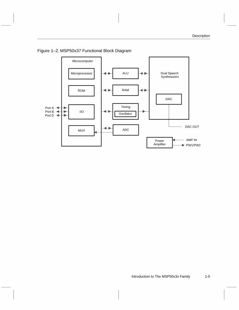
The MSP50x37 contains features not contained in the other members of theMSP50x3x family such as an integrated 8-bit successive approximation (SAR)analog-to-digital converter (ADC) with 8 to 1 analog multiplexer ports, a poweramplifier that has the capability to directly drive an 8-Ω speaker,a long intervaltimer and four I/O ports with sufficient drive capability to directly drive an LED.
Description
1-5 Introduction to The MSP50x3x Family
Figure 1–2. MSP50x37 Functional Block Diagram
Oscillator
Port A
Microcomputer
Timing
ALU
RAM
I/O
Microprocessor
ROM
Port B
Dual SpeechSynthesizers
DAC
ADC
Port D
MUX
PowerAmplifier
DAC OUT
AMP IN
PW1/PW2
Features
1-6
1.4 Features
The key features of the entire MSP50x3x family are in the following list.
Dual programmable LPC-12 speech synthesizers Simultaneous LPC and PCM 8-bit microprocessor with 61 instructions Thirty-two 12-bit words and 224 bytes of RAM 3.3V to 6.5V CMOS technology for low power dissipation Direct speaker drive capability Mask-selectable internal or external Clock Internal clock generator that requires no external components Two software-selectable clock speeds 10-kHz or 8-kHz speech sample rate Seven levels of stack Internal timer Externally-controlled interrupt Single-cycle multiply instruction Executes 1,200,000 instructions per second Built-in slave mode to act as a microprocessor peripheral Software-configurable wakeup function from any A Port I/O line
1.4.1 MSP50x32/33/34 Additional Features
MSP50x32/33/34 features not present in other family members include:
Ten software configurable I/O terminals (nine I/O terminals with externalclock selected)
Two digital-to-analog (D/A) configurations—mask selectable Several ROM/PROM configurations
16K bytes for MSP50C32 32K bytes for MSP50C33 64K bytes for MSP50C34 and MSP50P34
Features
1-7 Introduction to The MSP50x3x Family
1.4.2 MSP50x37 Additional Features
MSP50x37 features not present in other family members include:
Incorporated 8-bit analog-to-digital converter multiplexed to one of 8 I/Oports (D Ports)
18 software configurable I/O terminals Power amplifier for direct speaker drive (8 Ω /500 mW) 20-mA sink current for LED direct drive (A4 – A7) Additional long interval timer/counter Single-pin double-ended D/A output 16K-bytes of ROM/PROM
D/A Options
1-8
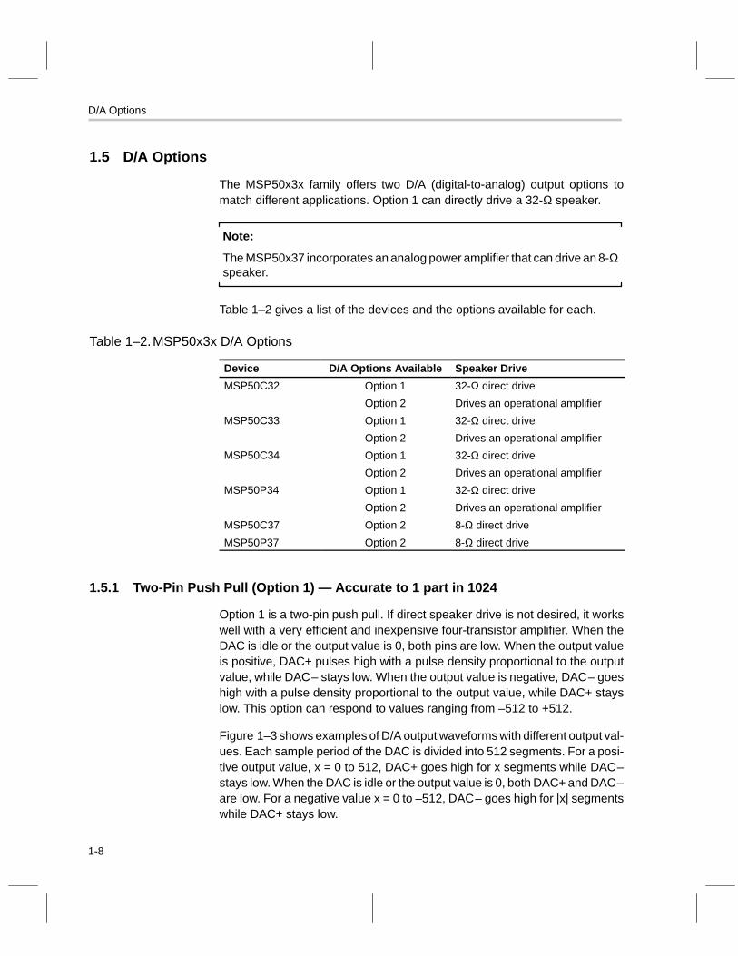
1.5 D/A Options
The MSP50x3x family offers two D/A (digital-to-analog) output options tomatch different applications. Option 1 can directly drive a 32-Ω speaker.
Note:
The MSP50x37 incorporates an analog power amplifier that can drive an 8-Ωspeaker.
Table 1–2 gives a list of the devices and the options available for each.
Table 1–2.MSP50x3x D/A Options
Device D/A Options Available Speaker Drive
MSP50C32 Option 1 32-Ω direct drive
Option 2 Drives an operational amplifier
MSP50C33 Option 1 32-Ω direct drive
Option 2 Drives an operational amplifier
MSP50C34 Option 1 32-Ω direct drive
Option 2 Drives an operational amplifier
MSP50P34 Option 1 32-Ω direct drive
Option 2 Drives an operational amplifier
MSP50C37 Option 2 8-Ω direct drive
MSP50P37 Option 2 8-Ω direct drive
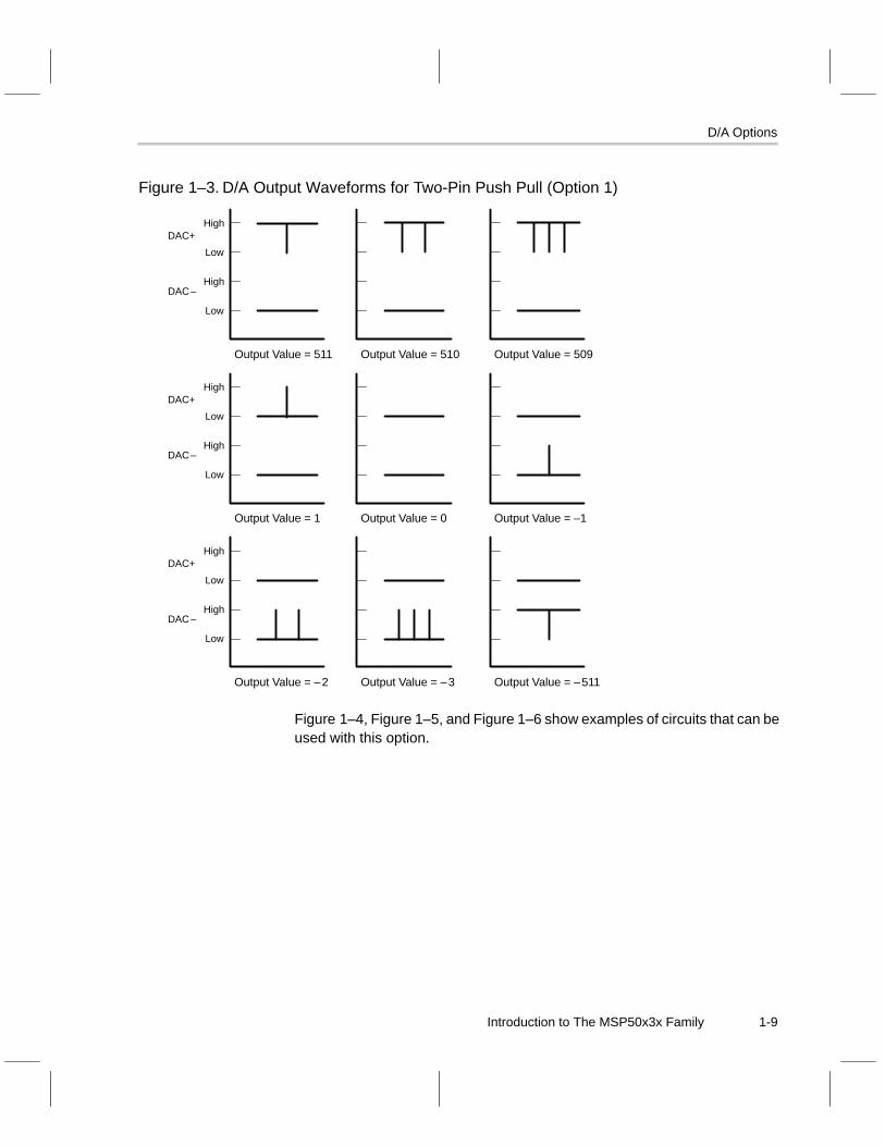
1.5.1 Two-Pin Push Pull (Option 1) — Accurate to 1 part in 1024
Option 1 is a two-pin push pull. If direct speaker drive is not desired, it workswell with a very efficient and inexpensive four-transistor amplifier. When theDAC is idle or the output value is 0, both pins are low. When the output valueis positive, DAC+ pulses high with a pulse density proportional to the outputvalue, while DAC– stays low. When the output value is negative, DAC– goeshigh with a pulse density proportional to the output value, while DAC+ stayslow. This option can respond to values ranging from –512 to +512.
Figure 1–3 shows examples of D/A output waveforms with different output val-ues. Each sample period of the DAC is divided into 512 segments. For a posi-tive output value, x = 0 to 512, DAC+ goes high for x segments while DAC–stays low. When the DAC is idle or the output value is 0, both DAC+ and DAC–are low. For a negative value x = 0 to –512, DAC– goes high for |x| segmentswhile DAC+ stays low.
D/A Options
1-9 Introduction to The MSP50x3x Family
Figure 1–3. D/A Output Waveforms for Two-Pin Push Pull (Option 1)
High
Low
High
Low
DAC+
DAC –
Output Value = 511 Output Value = 510 Output Value = 509
High
Low
High
Low
DAC+
DAC –
Output Value = 1 Output Value = 0 Output Value = –1
High
Low
High
Low
DAC+
DAC –
Output Value = –2 Output Value = –3 Output Value = –511
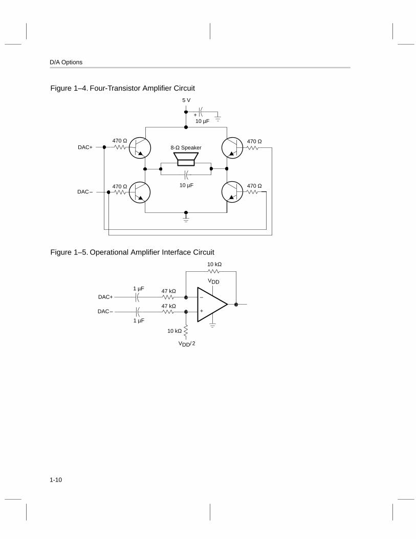
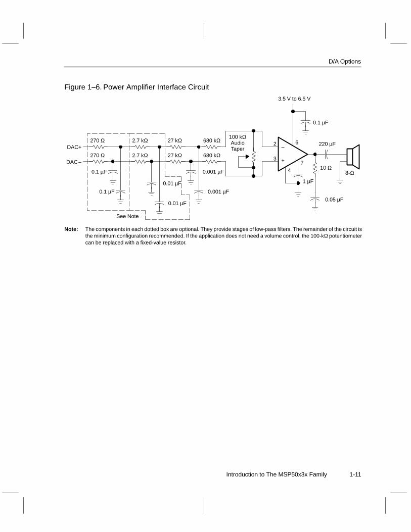
Figure 1–4, Figure 1–5, and Figure 1–6 show examples of circuits that can beused with this option.
D/A Options
1-10
Figure 1–4. Four-Transistor Amplifier Circuit
+
5 V
10 µF
470 Ω
470 Ω
470 Ω
470 Ω8-Ω SpeakerDAC+
DAC–10 µF
Figure 1–5. Operational Amplifier Interface Circuit
1 µF
+
–
47 kΩ
VDD
10 kΩ
10 kΩ
47 kΩ
1 µF
VDD/2
DAC+
DAC–
D/A Options
1-11 Introduction to The MSP50x3x Family
Figure 1–6. Power Amplifier Interface Circuit
DAC+
DAC–
8-Ω
3.5 V to 6.5 V
270 Ω
270 Ω
2.7 kΩ
2.7 kΩ
27 kΩ
27 kΩ
680 kΩ
680 kΩ
100 kΩAudioTaper
+
–2
3
6
47
1 µF
10 Ω
220 µF
0.1 µF
0.1 µF
0.1 µF
0.01 µF
0.001 µF
0.001 µF
0.01 µF
0.05 µF
See Note
Note: The components in each dotted box are optional. They provide stages of low-pass filters. The remainder of the circuit isthe minimum configuration recommended. If the application does not need a volume control, the 100-kΩ potentiometercan be replaced with a fixed-value resistor.
D/A Options
1-12
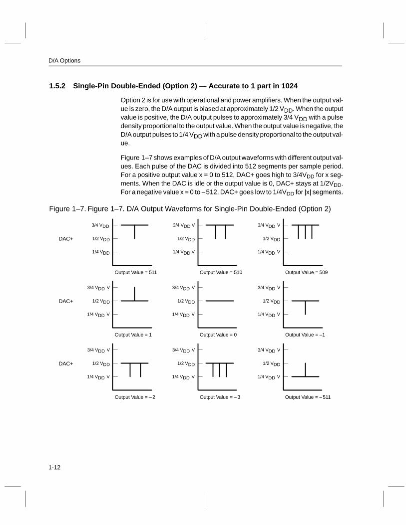
1.5.2 Single-Pin Double-Ended (Option 2) — Accurate to 1 part in 1024
Option 2 is for use with operational and power amplifiers. When the output val-ue is zero, the D/A output is biased at approximately 1/2 VDD. When the outputvalue is positive, the D/A output pulses to approximately 3/4 VDD with a pulsedensity proportional to the output value. When the output value is negative, theD/A output pulses to 1/4 VDD with a pulse density proportional to the output val-ue.
Figure 1–7 shows examples of D/A output waveforms with different output val-ues. Each pulse of the DAC is divided into 512 segments per sample period.For a positive output value x = 0 to 512, DAC+ goes high to 3/4VDD for x seg-ments. When the DAC is idle or the output value is 0, DAC+ stays at 1/2VDD.For a negative value x = 0 to –512, DAC+ goes low to 1/4VDD for |x| segments.
Figure 1–7. Figure 1–7. D/A Output Waveforms for Single-Pin Double-Ended (Option 2)
DAC+
Output Value = 511
3/4 VDD V
1/2 VDD
1/4 VDD V
DAC+
Output Value = 1
3/4 VDD
1/2 VDD
1/4 VDD
3/4 VDD V
1/2 VDD
1/4 VDD V
Output Value = 0
3/4 VDD V
1/2 VDD
1/4 VDD V
Output Value = 510
3/4 VDD V
1/2 VDD
1/4 VDD V
Output Value = –1
3/4 VDD V
1/2 VDD
1/4 VDD V
Output Value = 509
DAC+
3/4 VDD V
1/2 VDD
1/4 VDD V
Output Value = –2
3/4 VDD V
1/2 VDD
1/4 VDD V
Output Value = –3
3/4 VDD V
1/2 VDD
1/4 VDD V
Output Value = –511
D/A Options
1-13 Introduction to The MSP50x3x Family
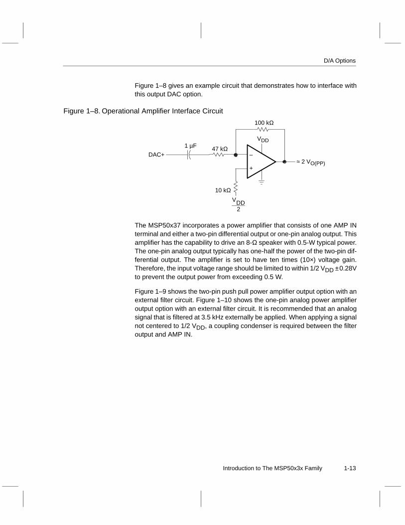
Figure 1–8 gives an example circuit that demonstrates how to interface withthis output DAC option.
Figure 1–8. Operational Amplifier Interface Circuit
1 µF
+
–
VDD
100 kΩ
10 kΩ
47 kΩ
≈ 2 VO(PP)
DAC+
VDD2
The MSP50x37 incorporates a power amplifier that consists of one AMP INterminal and either a two-pin differential output or one-pin analog output. Thisamplifier has the capability to drive an 8-Ω speaker with 0.5-W typical power.The one-pin analog output typically has one-half the power of the two-pin dif-ferential output. The amplifier is set to have ten times (10×) voltage gain.Therefore, the input voltage range should be limited to within 1/2 VDD ±0.28Vto prevent the output power from exceeding 0.5 W.
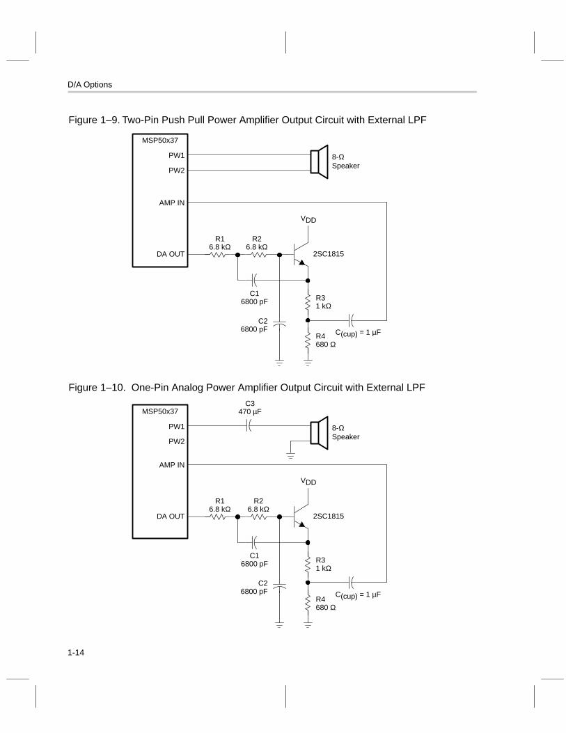
Figure 1–9 shows the two-pin push pull power amplifier output option with anexternal filter circuit. Figure 1–10 shows the one-pin analog power amplifieroutput option with an external filter circuit. It is recommended that an analogsignal that is filtered at 3.5 kHz externally be applied. When applying a signalnot centered to 1/2 VDD, a coupling condenser is required between the filteroutput and AMP IN.
D/A Options
1-14
Figure 1–9. Two-Pin Push Pull Power Amplifier Output Circuit with External LPF
PW1
PW2
R16.8 kΩ
C16800 pF
8-ΩSpeaker
MSP50x37
AMP IN
DA OUT
R26.8 kΩ
C26800 pF
VDD
2SC1815
R31 kΩ
R4680 Ω
C(cup) = 1 µF
Figure 1–10. One-Pin Analog Power Amplifier Output Circuit with External LPF
PW1
PW2
R16.8 kΩ
C16800 pF
8-ΩSpeaker
MSP50x37
AMP IN
DA OUT
R26.8 kΩ
C26800 pF
C3470 µF
VDD
2SC1815
R31 kΩ
R4680 Ω
C(cup) = 1 µF
Terminal Assignments and Signal Descriptions
1-15 Introduction to The MSP50x3x Family
1.6 Terminal Assignments and Signal Descriptions
The following sections give terminal assignment and signal description in-formation for the MSP50x3x family. The MSP50x32/33/34 are all available ina 16-pin DW or N package and in die form. The MSP50P34 is also availablein a 40-pin NW package, which is used for engineering evaluation. TheMSP50x37 is available in a 28-pin DW package.
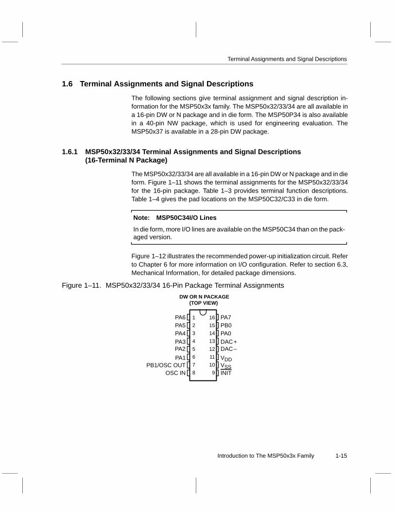
1.6.1 MSP50x32/33/34 Terminal Assignments and Signal Descriptions (16-Terminal N Package)
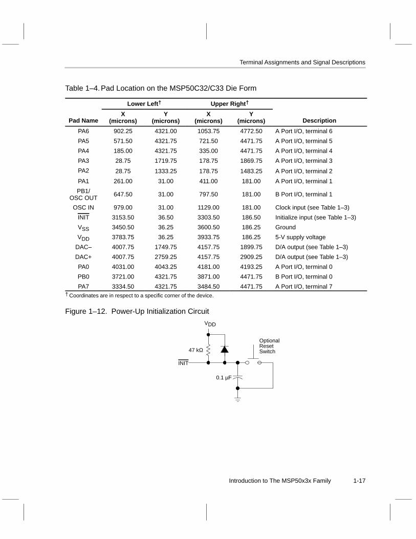
The MSP50x32/33/34 are all available in a 16-pin DW or N package and in dieform. Figure 1–11 shows the terminal assignments for the MSP50x32/33/34for the 16-pin package. Table 1–3 provides terminal function descriptions.Table 1–4 gives the pad locations on the MSP50C32/C33 in die form.
Note: MSP50C34I/O Lines
In die form, more I/O lines are available on the MSP50C34 than on the pack-aged version.
Figure 1–12 illustrates the recommended power-up initialization circuit. Referto Chapter 6 for more information on I/O configuration. Refer to section 6.3,Mechanical Information, for detailed package dimensions.
Figure 1–11. MSP50x32/33/34 16-Pin Package Terminal Assignments
1
2
3
4
5
6
7
8
16
15
14
13
12
11
10
9
DW OR N PACKAGE(TOP VIEW)
OSC IN
PA6PA5PA4PA3PA2
PA1PB1/OSC OUT
PA7PB0PA0DAC+DAC–
VDDVSSINIT
Terminal Assignments and Signal Descriptions
1-16
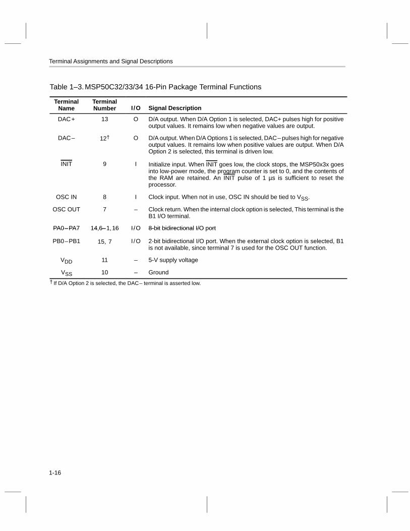
Table 1–3.MSP50C32/33/34 16-Pin Package Terminal Functions
TerminalName
TerminalNumber I /O Signal Description
DAC+ 13 O D/A output. When D/A Option 1 is selected, DAC+ pulses high for positiveoutput values. It remains low when negative values are output.
DAC– 12† O D/A output. When D/A Options 1 is selected, DAC– pulses high for negativeoutput values. It remains low when positive values are output. When D/AOption 2 is selected, this terminal is driven low.
INIT 9 I Initialize input. When INIT goes low, the clock stops, the MSP50x3x goesinto low-power mode, the program counter is set to 0, and the contents ofthe RAM are retained. An INIT pulse of 1 µs is sufficient to reset theprocessor.
OSC IN 8 I Clock input. When not in use, OSC IN should be tied to VSS.
OSC OUT 7 – Clock return. When the internal clock option is selected, This terminal is theB1 I/O terminal.
PA0–PA7 14 6–1 16 I /O 8-bit bidirectional I/O portPA0–PA7 14,6–1,16 I /O 8-bit bidirectional I/O ort
PB0–PB1 15, 7 I /O 2-bit bidirectional I/O port. When the external clock option is selected, B1is not available, since terminal 7 is used for the OSC OUT function.
VDD 11 – 5-V supply voltage
VSS 10 – Ground
† If D/A Option 2 is selected, the DAC– terminal is asserted low.
Terminal Assignments and Signal Descriptions
1-17 Introduction to The MSP50x3x Family
Table 1–4.Pad Location on the MSP50C32/C33 Die Form
Lower Left† Upper Right†
Pad NameX
(microns)Y
(microns)X
(microns)Y
(microns) Description
PA6 902.25 4321.00 1053.75 4772.50 A Port I/O, terminal 6
PA5 571.50 4321.75 721.50 4471.75 A Port I/O, terminal 5
PA4 185.00 4321.75 335.00 4471.75 A Port I/O, terminal 4
PA3 28.75 1719.75 178.75 1869.75 A Port I/O, terminal 3
PA2 28.75 1333.25 178.75 1483.25 A Port I/O, terminal 2
PA1 261.00 31.00 411.00 181.00 A Port I/O, terminal 1
PB1/OSC OUT
647.50 31.00 797.50 181.00 B Port I/O, terminal 1
OSC IN 979.00 31.00 1129.00 181.00 Clock input (see Table 1–3)
INIT 3153.50 36.50 3303.50 186.50 Initialize input (see Table 1–3)
VSS 3450.50 36.25 3600.50 186.25 Ground
VDD 3783.75 36.25 3933.75 186.25 5-V supply voltage
DAC– 4007.75 1749.75 4157.75 1899.75 D/A output (see Table 1–3)
DAC+ 4007.75 2759.25 4157.75 2909.25 D/A output (see Table 1–3)
PA0 4031.00 4043.25 4181.00 4193.25 A Port I/O, terminal 0
PB0 3721.00 4321.75 3871.00 4471.75 B Port I/O, terminal 0
PA7 3334.50 4321.75 3484.50 4471.75 A Port I/O, terminal 7† Coordinates are in respect to a specific corner of the device.
Figure 1–12. Power-Up Initialization Circuit
0.1 µF
47 kΩ
OptionalResetSwitch
INIT
VDD
Terminal Assignments and Signal Descriptions
1-18
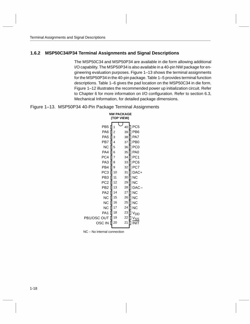
1.6.2 MSP50C34/P34 Terminal Assignments and Signal Descriptions
The MSP50C34 and MSP50P34 are available in die form allowing additionalI/O capability. The MSP50P34 is also available in a 40-pin NW package for en-gineering evaluation purposes. Figure 1–13 shows the terminal assignmentsfor the MSP50P34 in the 40-pin package. Table 1–5 provides terminal functiondescriptions. Table 1–6 gives the pad location on the MSP50C34 in die form.Figure 1–12 illustrates the recommended power up initialization circuit. Referto Chapter 6 for more information on I/O configuration. Refer to section 6.3,Mechanical Information, for detailed package dimensions.
Figure 1–13. MSP50P34 40-Pin Package Terminal Assignments
1
2
3
4
5
6
7
8
9
10
11
12
13
14
15
16
17
18
19
20
40
39
38
37
36
35
34
33
32
31
30
29
28
27
26
25
24
23
22
21
PB5PA6PA5PB7NC
PA4PC4PA3PB4PC3PB3PC2PB2PA2NCNCNC
PA1PB1/OSC OUT
OSC IN
PC5PB6PA7PB0PC0PA0PC1PC6PC7DAC+NCNCDAC–NCNCNCNCVDDVSSINIT
NW PACKAGE(TOP VIEW)
NC – No internal connection
Terminal Assignments and Signal Descriptions
1-19 Introduction to The MSP50x3x Family
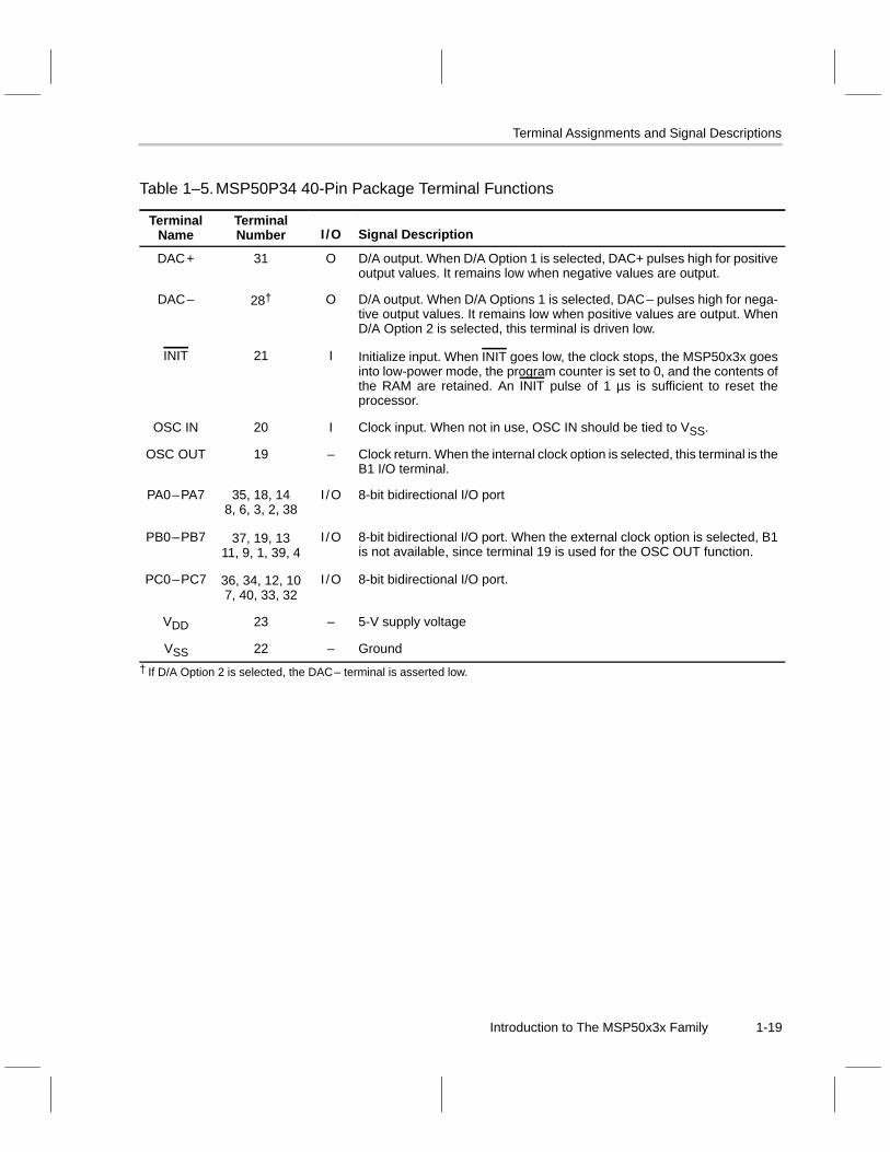
Table 1–5.MSP50P34 40-Pin Package Terminal Functions
TerminalName
TerminalNumber I /O Signal Description
DAC+ 31 O D/A output. When D/A Option 1 is selected, DAC+ pulses high for positiveoutput values. It remains low when negative values are output.
DAC– 28† O D/A output. When D/A Options 1 is selected, DAC– pulses high for nega-tive output values. It remains low when positive values are output. WhenD/A Option 2 is selected, this terminal is driven low.
INIT 21 I Initialize input. When INIT goes low, the clock stops, the MSP50x3x goesinto low-power mode, the program counter is set to 0, and the contents ofthe RAM are retained. An INIT pulse of 1 µs is sufficient to reset theprocessor.
OSC IN 20 I Clock input. When not in use, OSC IN should be tied to VSS.
OSC OUT 19 – Clock return. When the internal clock option is selected, this terminal is theB1 I/O terminal.
PA0–PA7 35, 18, 14 I /O 8-bit bidirectional I/O port8, 6, 3, 2, 38
PB0–PB7 37, 19, 1311, 9, 1, 39, 4
I /O 8-bit bidirectional I/O port. When the external clock option is selected, B1is not available, since terminal 19 is used for the OSC OUT function.
PC0–PC7 36, 34, 12, 107, 40, 33, 32
I /O 8-bit bidirectional I/O port.
VDD 23 – 5-V supply voltage
VSS 22 – Ground
† If D/A Option 2 is selected, the DAC– terminal is asserted low.
Terminal Assignments and Signal Descriptions
1-20
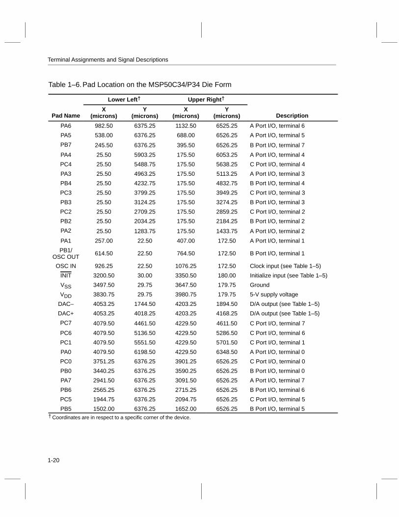
Table 1–6.Pad Location on the MSP50C34/P34 Die Form
Lower Left† Upper Right†
Pad NameX
(microns)Y
(microns)X
(microns)Y
(microns) Description
PA6 982.50 6375.25 1132.50 6525.25 A Port I/O, terminal 6
PA5 538.00 6376.25 688.00 6526.25 A Port I/O, terminal 5
PB7 245.50 6376.25 395.50 6526.25 B Port I/O, terminal 7
PA4 25.50 5903.25 175.50 6053.25 A Port I/O, terminal 4
PC4 25.50 5488.75 175.50 5638.25 C Port I/O, terminal 4
PA3 25.50 4963.25 175.50 5113.25 A Port I/O, terminal 3
PB4 25.50 4232.75 175.50 4832.75 B Port I/O, terminal 4
PC3 25.50 3799.25 175.50 3949.25 C Port I/O, terminal 3
PB3 25.50 3124.25 175.50 3274.25 B Port I/O, terminal 3
PC2 25.50 2709.25 175.50 2859.25 C Port I/O, terminal 2
PB2 25.50 2034.25 175.50 2184.25 B Port I/O, terminal 2
PA2 25.50 1283.75 175.50 1433.75 A Port I/O, terminal 2
PA1 257.00 22.50 407.00 172.50 A Port I/O, terminal 1
PB1/OSC OUT
614.50 22.50 764.50 172.50 B Port I/O, terminal 1
OSC IN 926.25 22.50 1076.25 172.50 Clock input (see Table 1–5)
INIT 3200.50 30.00 3350.50 180.00 Initialize input (see Table 1–5)
VSS 3497.50 29.75 3647.50 179.75 Ground
VDD 3830.75 29.75 3980.75 179.75 5-V supply voltage
DAC– 4053.25 1744.50 4203.25 1894.50 D/A output (see Table 1–5)
DAC+ 4053.25 4018.25 4203.25 4168.25 D/A output (see Table 1–5)
PC7 4079.50 4461.50 4229.50 4611.50 C Port I/O, terminal 7
PC6 4079.50 5136.50 4229.50 5286.50 C Port I/O, terminal 6
PC1 4079.50 5551.50 4229.50 5701.50 C Port I/O, terminal 1
PA0 4079.50 6198.50 4229.50 6348.50 A Port I/O, terminal 0
PC0 3751.25 6376.25 3901.25 6526.25 C Port I/O, terminal 0
PB0 3440.25 6376.25 3590.25 6526.25 B Port I/O, terminal 0
PA7 2941.50 6376.25 3091.50 6526.25 A Port I/O, terminal 7
PB6 2565.25 6376.25 2715.25 6526.25 B Port I/O, terminal 6
PC5 1944.75 6376.25 2094.75 6526.25 C Port I/O, terminal 5
PB5 1502.00 6376.25 1652.00 6526.25 B Port I/O, terminal 5† Coordinates are in respect to a specific corner of the device.
Terminal Assignments and Signal Descriptions
1-21 Introduction to The MSP50x3x Family
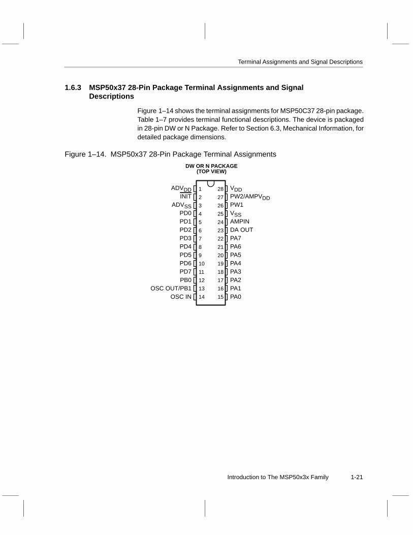
1.6.3 MSP50x37 28-Pin Package Terminal Assignments and Signal Descriptions
Figure 1–14 shows the terminal assignments for MSP50C37 28-pin package.Table 1–7 provides terminal functional descriptions. The device is packagedin 28-pin DW or N Package. Refer to Section 6.3, Mechanical Information, fordetailed package dimensions.
Figure 1–14. MSP50x37 28-Pin Package Terminal Assignments
1
2
3
4
5
6
7
8
9
10
11
12
13
14
28
27
26
25
24
23
22
21
20
19
18
17
16
15
ADVDDINIT
ADVSSPD0PD1PD2PD3PD4PD5PD6PD7PB0
OSC OUT/PB1OSC IN
VDDPW2/AMPVDDPW1VSSAMPINDA OUTPA7PA6PA5PA4PA3PA2PA1PA0
DW OR N PACKAGE(TOP VIEW)
Terminal Assignments and Signal Descriptions
1-22
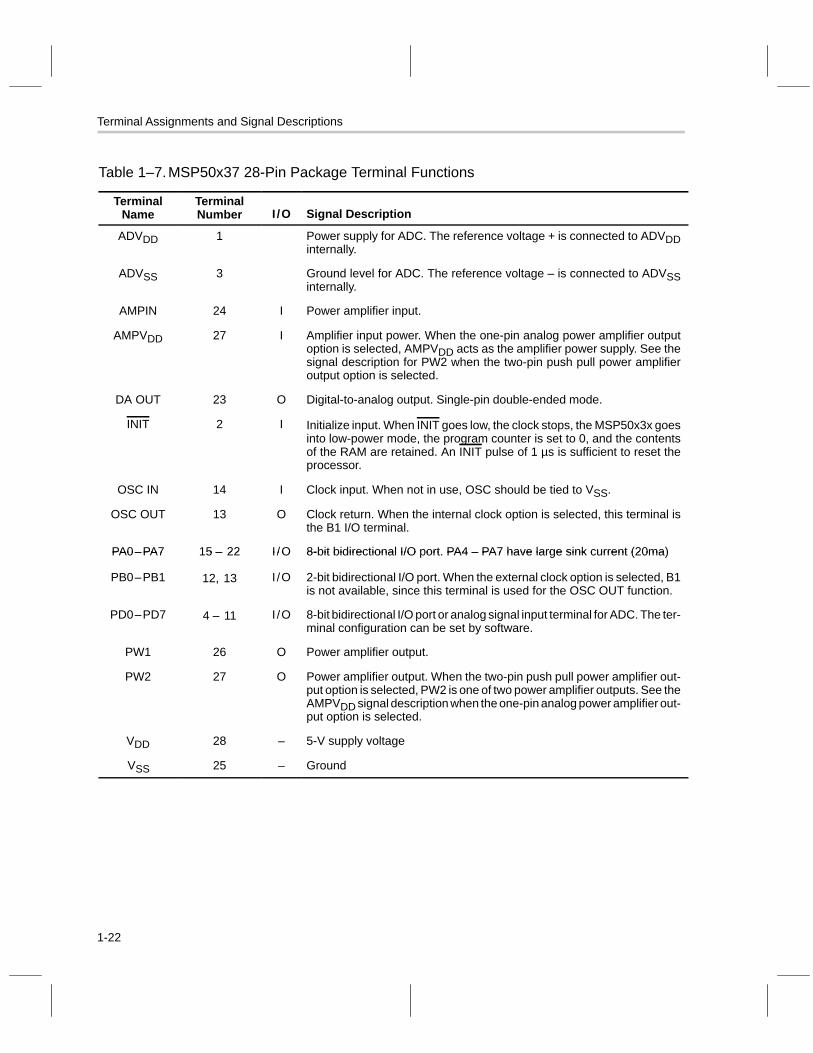
Table 1–7.MSP50x37 28-Pin Package Terminal Functions
TerminalName
TerminalNumber I /O Signal Description
ADVDD 1 Power supply for ADC. The reference voltage + is connected to ADVDDinternally.
ADVSS 3 Ground level for ADC. The reference voltage – is connected to ADVSSinternally.
AMPIN 24 I Power amplifier input.
AMPVDD 27 I Amplifier input power. When the one-pin analog power amplifier outputoption is selected, AMPVDD acts as the amplifier power supply. See thesignal description for PW2 when the two-pin push pull power amplifieroutput option is selected.
DA OUT 23 O Digital-to-analog output. Single-pin double-ended mode.
INIT 2 I Initialize input. When INIT goes low, the clock stops, the MSP50x3x goesinto low-power mode, the program counter is set to 0, and the contentsof the RAM are retained. An INIT pulse of 1 µs is sufficient to reset theprocessor.
OSC IN 14 I Clock input. When not in use, OSC should be tied to VSS.
OSC OUT 13 O Clock return. When the internal clock option is selected, this terminal isthe B1 I/O terminal.
PA0–PA7 15 – 22 I /O 8-bit bidirectional I/O port PA4 – PA7 have large sink current (20ma)PA0–PA7 15 – 22 I /O 8-bit bidirectional I/O ort. PA4 – PA7 have large sink current (20ma)
PB0–PB1 12, 13 I /O 2-bit bidirectional I/O port. When the external clock option is selected, B1is not available, since this terminal is used for the OSC OUT function.
PD0–PD7 4 – 11 I /O 8-bit bidirectional I/O port or analog signal input terminal for ADC. The ter-minal configuration can be set by software.
PW1 26 O Power amplifier output.
PW2 27 O Power amplifier output. When the two-pin push pull power amplifier out-put option is selected, PW2 is one of two power amplifier outputs. See theAMPVDD signal description when the one-pin analog power amplifier out-put option is selected.
VDD 28 – 5-V supply voltage
VSS 25 – Ground
Introduction to Linear Predictive Coding (LPC)
1-23 Introduction to The MSP50x3x Family
1.7 Introduction to Linear Predictive Coding (LPC)
The LPC-12 system uses a mathematical model of the human vocal tract toenable efficient digital storage and recreation of realistic speech. To under-stand LPC, it is essential to understand how the vocal tract works. Thisintroduction, therefore, begins with a short description of the vocal tract, afterwhich the LPC model and data compression techniques are addressed.
1.7.1 The Vocal Tract
Speech is the result of the interaction among three elements in the vocal tract;air from the lungs, a restriction that converts the airflow to sound, and the vocalcavities that are positioned to resonate properly.
Air from the lungs is expelled through the vocal tract when the muscles of thechest and diaphragm are compressed. Pressure is used as a volume control,with higher pressure for louder speech.
As air flows through the vocal tract, it makes little sound if there is no restriction.The vocal cords are one type of restriction. They can be tightened across thevocal tract to stop the flow of air. Pressure builds up behind them and forcesthem open. This happens over and over, generating a series of pulses. Thetension on the vocal cords can be varied to change the frequency of the pulses.Many speech sounds, such as the “A” sound, are produced by this type of re-striction, which is called “voiced” speech.
A different type of restriction in the mouth causes a hissing sound called whitenoise. The “S” sound is a good example. White noise occurs when the tongueand some part of the mouth are in close contact or when the lips are pursed.This restriction causes high flow velocities that cause turbulence producingwhite noise, which is called “unvoiced” speech.
The pulses from the vocal cords and the noise from the turbulence have fairlybroad, flat spectral characteristics. In other words, they are noise, not speech.The shape of the oral cavity changes noise into recognizable speech. Thepositions of the tongue, the lips, and the jaws change the resonance of the vo-cal tract, shaping the raw noise of restricted airflow into understandablesounds.
1.7.2 The LPC Model
The LPC model incorporates elements analogous to each of the elements ofthe vocal tract described above. It has an excitation function generator thatmodels both types of restriction, a gain multiplication stage to model the pos-sible levels of pressure from the lungs, and a digital filter to model the reso-nance in the oral and nasal cavities.
Introduction to Linear Predictive Coding (LPC)
1-24
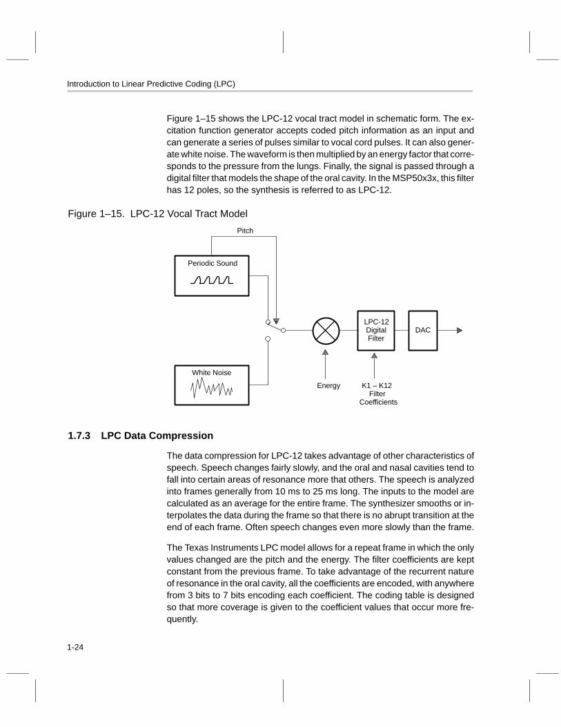
Figure 1–15 shows the LPC-12 vocal tract model in schematic form. The ex-citation function generator accepts coded pitch information as an input andcan generate a series of pulses similar to vocal cord pulses. It can also gener-ate white noise. The waveform is then multiplied by an energy factor that corre-sponds to the pressure from the lungs. Finally, the signal is passed through adigital filter that models the shape of the oral cavity. In the MSP50x3x, this filterhas 12 poles, so the synthesis is referred to as LPC-12.
Figure 1–15. LPC-12 Vocal Tract Model
LPC-12DigitalFilter
DAC
Periodic Sound
White Noise
K1 – K12Filter
Coefficients
Energy
Pitch
1.7.3 LPC Data Compression
The data compression for LPC-12 takes advantage of other characteristics ofspeech. Speech changes fairly slowly, and the oral and nasal cavities tend tofall into certain areas of resonance more that others. The speech is analyzedinto frames generally from 10 ms to 25 ms long. The inputs to the model arecalculated as an average for the entire frame. The synthesizer smooths or in-terpolates the data during the frame so that there is no abrupt transition at theend of each frame. Often speech changes even more slowly than the frame.
The Texas Instruments LPC model allows for a repeat frame in which the onlyvalues changed are the pitch and the energy. The filter coefficients are keptconstant from the previous frame. To take advantage of the recurrent natureof resonance in the oral cavity, all the coefficients are encoded, with anywherefrom 3 bits to 7 bits encoding each coefficient. The coding table is designedso that more coverage is given to the coefficient values that occur more fre-quently.
MSP50x3x Mask Options
1-25 Introduction to The MSP50x3x Family
1.8 MSP50x3x Mask Options
The MSP50x3x can be configured to suit different applications with a varietyof mask options.
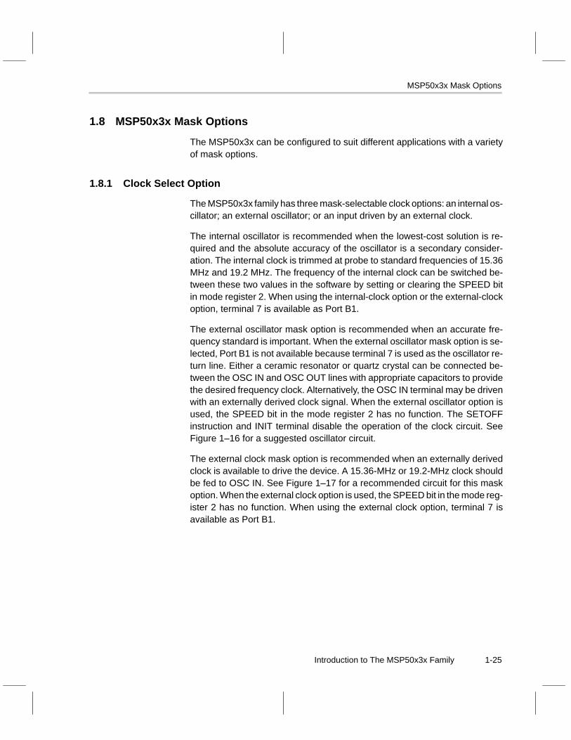
1.8.1 Clock Select Option
The MSP50x3x family has three mask-selectable clock options: an internal os-cillator; an external oscillator; or an input driven by an external clock.
The internal oscillator is recommended when the lowest-cost solution is re-quired and the absolute accuracy of the oscillator is a secondary consider-ation. The internal clock is trimmed at probe to standard frequencies of 15.36MHz and 19.2 MHz. The frequency of the internal clock can be switched be-tween these two values in the software by setting or clearing the SPEED bitin mode register 2. When using the internal-clock option or the external-clockoption, terminal 7 is available as Port B1.
The external oscillator mask option is recommended when an accurate fre-quency standard is important. When the external oscillator mask option is se-lected, Port B1 is not available because terminal 7 is used as the oscillator re-turn line. Either a ceramic resonator or quartz crystal can be connected be-tween the OSC IN and OSC OUT lines with appropriate capacitors to providethe desired frequency clock. Alternatively, the OSC IN terminal may be drivenwith an externally derived clock signal. When the external oscillator option isused, the SPEED bit in the mode register 2 has no function. The SETOFFinstruction and INIT terminal disable the operation of the clock circuit. SeeFigure 1–16 for a suggested oscillator circuit.
The external clock mask option is recommended when an externally derivedclock is available to drive the device. A 15.36-MHz or 19.2-MHz clock shouldbe fed to OSC IN. See Figure 1–17 for a recommended circuit for this maskoption. When the external clock option is used, the SPEED bit in the mode reg-ister 2 has no function. When using the external clock option, terminal 7 isavailable as Port B1.
MSP50x3x Mask Options
1-26
Figure 1–16. Oscillator Circuit
30 pF30 pF
OSC IN OSC OUTINIT
Crystal or Ceramic Resonator
MSP50x3x
Figure 1–17. External Clock Interface
OSC IN OSC OUTINIT
MSP50x3x
Clock In 500 Ω
1.8.2 DAC Option
The DAC for the MSP50C32/33/34 can be selected as either a two-pin pushpull or a one-pin analog. The MSP50C37 has only one output option, the one-pin analog power amplifier output option. See Section 1.5, D/A Options, formore information.
MSP50x3x Mask Options
1-27 Introduction to The MSP50x3x Family
1.8.3 Power Amplifier Options (MSP50C37 Only)
The MSP50C37 has two mask-selectable power amplifier output options: aone-pin analog and a two-pin push pull differential. When the one-pin analogoption is selected, the PW1 terminal is the power amplifier output and thePW2/AMPVDD is the power amplifier current supply. When the two-pin push-pull option is selected, PW1 and PW2/AMPVDD are the power amplifier differ-ential outputs. For both options, the amplifier voltage gain is 10×.

1-28
2-1
MSP50x3x Family Architecture
This chapter describes the architecture and function of the MSP50x3x familyof speech synthesizers including RAM, ROM, registers, flags, and the DAC.
Topic Page
2.1 MSP50C3x Family Architecture 2-2. . . . . . . . . . . . . . . . . . . . . . . . . . . . . . . . .
2.2 Speech Synthesis 2-22
2.3 Interrupts 2-27
2.4 MSP50C3x Power Control and Initialization 2-29
2.5 MSP50C3x Clocks 2-30
2.6 Analog-to-Digital Converter (MSP50x37 Only) 2-32
2.7 Power Amplifier (MSP50x37 Only) 2-33
Chapter 2
MSP50C3x Family Architecture
2-2
2.1 MSP50C3x Family Architecture
As shown in the block diagram in Figure 2–1, the major components of theMSP50C3x are a speech synthesizer; an 8-bit microprocessor; an internal16K byte (MSP50C32), 32K byte (MSP50C33), or 64K byte (MSP50C34)ROM; and input/output ports.
The system clock can be internally generated or be driven externally. Whenthe internal clock is used, the clock operates under software control and canbe programmed to one of two frequencies, 19.2 MHz (used when LPC isoperating at 10,000 samples per second) or 15.36 MHz (for 8,000 samples persecond). If the internally generated frequencies are not sufficiently accurate,the device can be configured with a mask option to provide custom frequencyoperation using an external clock signal, an external ceramic resonator, or aquartz crystal (with appropriate capacitors).
When LPC synthesis is disabled, instructions are fetched by themicroprocessor at 1/16 of the clock frequency. These instructions control theactions of the MSP50C3x. By placing different instruction patterns in the ROM,the MSP50C3x can be programmed to accomplish a wide variety of tasks. Togenerate speech, the processor accesses speech data from the internal ROMinternal RAM, or some external source. Once the data has been read, theprocessor must unpack and decode the individual speech parameters andstore the results in a dedicated section of the RAM.
The synthesizer shares access to the RAM and addresses the individualparameter locations as needed when generating speech. Each LPCsynthesizer uses approximately one quarter of the available instruction cycleswhen enabled. The instruction execution rate slows to 3/4 when one LPCsynthesizer is enabled and to 1/2 when both LPC synthesizers are enabled.
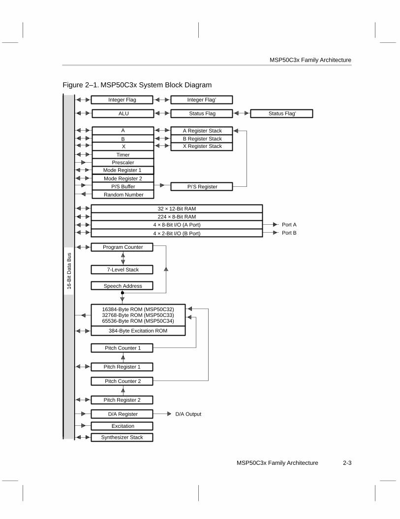
MSP50C3x Family Architecture
2-3 MSP50C3x Family Architecture
Figure 2–1. MSP50C3x System Block Diagram
Synthesizer Stack
Integer Flag Integer Flag’
A
B
Timer
Prescaler
Mode Register 2
P/S Buffer
Random Number
X
ALU Status Flag’
A Register Stack
B Register StackX Register Stack
32 × 12-Bit RAM
224 × 8-Bit RAM
4 × 8-Bit I/O (A Port)
4 × 2-Bit I/O (B Port)
Program Counter
7-Level Stack
Speech Address
Pitch Counter 1
D/A Register
Excitation
16-B
it D
ata
Bus
Pitch Register 1
Status Flag
Port A
Port B
P/S Register
D/A Output
16384-Byte ROM (MSP50C32)32768-Byte ROM (MSP50C33)65536-Byte ROM (MSP50C34)
384-Byte Excitation ROM
Pitch Counter 2
Pitch Register 2
Mode Register 1
MSP50C3x Family Architecture
2-4
The block diagram in Figure 2–2 shows that the MSP50x37 consists of theMSP50C3x core, several I/O ports (A, B, and D), 16K-byte ROM (MSP50C37)or PROM (MSP50P37), an 8-bit A/D converter with an analog multiplexer thatis connected to the D Port and power amplifier.
Since the device is structured based on the MSP50C3x core, most of the fea-tures associated with performance of the core, such as clock speed, instruc-tion cycle, RAM structure, speech synthesizer operations, etc., are the sameas those of the MSP50x32/33/34.
Figure 2–2. MSP50x37 System Block Diagram
MSP50C3xCore
4 × 8-Bit I/O (A Port)
4 × 2-Bit I/O (B Port)
–4 × 8-Bit I/O (D Port)
ADC
16-B
it D
ata
Bus
Power Amplifier
Port A
Port B
16K-Byte ROM (MSP50C37) or16K-Byte PROM (MSP50P37)
8-Bit Presaler Register /16-Bit Timer
Port D
MUX
AMP IN
P–AMP OUT(PW1, PW2)
2.1.1 Read-Only Memory (ROM)
The MSP50C32 has 16K-bytes of ROM. The MSP50C33 has a 32K-byteROM. The MSP50C34 has a 64K-byte ROM and the MSP50P34 has 64K-by-tes of PROM. The MSP50C37 has 16K-bytes of ROM, and the MSP50P37 has16K-bytes of PROM. The MSP50C3x can program instructions and speechdata as required by the application. Certain locations in the ROM, describedin Table 2–1, are reserved for specific purposes.
MSP50C3x Family Architecture
2-5 MSP50C3x Family Architecture
Table 2–1.Reserved ROM Locations
Address Function
0000h Execution start location after INIT rising edge
0002h Execution start location after I/O wakeup falling edge
0010h – 001Fh Interrupt start locations (see Section 2.3, Interrupts)
3FDBh – 3FFFh Texas Instruments test code (MSP50C32/37)
7FDBh – 7FFFh Texas Instruments test code (MSP50C33)
FFDBh – FFFFh Texas Instruments test code (MSP50C34)
The ROM can be accessed in the following four ways:
The program counter addresses processor instructions (see Chapter 4 forinstruction definitions).
The GET instruction transfers 1 to 8 bits from the ROM to the A register.The GET counter is initialized by the LUAPS instruction. The SAR (speechaddress register) points to the ROM location to be used.
The LUAA instruction transfers a byte from the ROM into the A register.The value in the A register when LUAA is executed points to the ROM ad-dress to be used.
The LUAB instruction transfers a byte from the ROM into the B register.The value in the A register when LUAB is executed points to the ROM ad-dress to be used.
2.1.2 Program Counter
The MSP50C3x has a 16-bit program counter that points to the next instructionto be executed. After the instruction is executed, the program counter is nor-mally incremented to point to the next instruction.
When an interrupt occurs, the program counter is loaded with the interrupt vec-tor address; where execution resumes. See Section 2.3, Interrupts, for moreinformation. The following instructions modify the program counter:
BR Branch BRA Branch to address in A register SBR Short branch RETN Return from subroutine RETI Return from interrupt CALL Subroutine Call
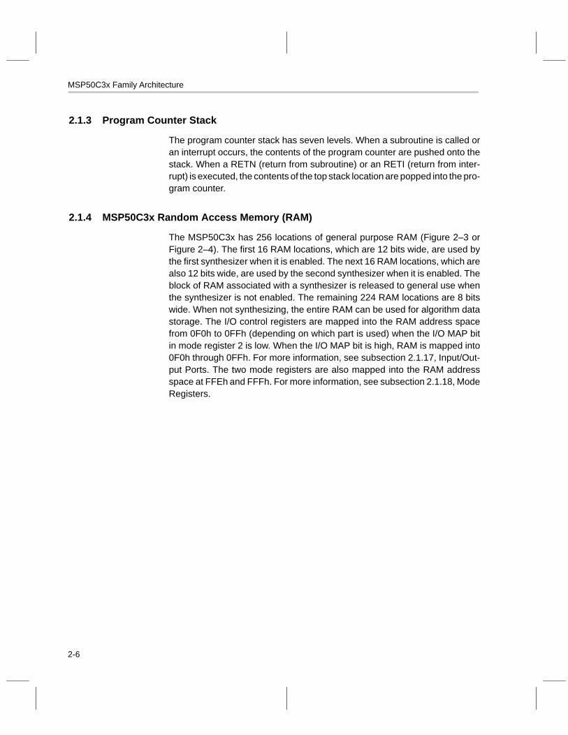
MSP50C3x Family Architecture
2-6
2.1.3 Program Counter Stack
The program counter stack has seven levels. When a subroutine is called oran interrupt occurs, the contents of the program counter are pushed onto thestack. When a RETN (return from subroutine) or an RETI (return from inter-rupt) is executed, the contents of the top stack location are popped into the pro-gram counter.
2.1.4 MSP50C3x Random Access Memory (RAM)
The MSP50C3x has 256 locations of general purpose RAM (Figure 2–3 orFigure 2–4). The first 16 RAM locations, which are 12 bits wide, are used bythe first synthesizer when it is enabled. The next 16 RAM locations, which arealso 12 bits wide, are used by the second synthesizer when it is enabled. Theblock of RAM associated with a synthesizer is released to general use whenthe synthesizer is not enabled. The remaining 224 RAM locations are 8 bitswide. When not synthesizing, the entire RAM can be used for algorithm datastorage. The I/O control registers are mapped into the RAM address spacefrom 0F0h to 0FFh (depending on which part is used) when the I/O MAP bitin mode register 2 is low. When the I/O MAP bit is high, RAM is mapped into0F0h through 0FFh. For more information, see subsection 2.1.17, Input/Out-put Ports. The two mode registers are also mapped into the RAM addressspace at FFEh and FFFh. For more information, see subsection 2.1.18, ModeRegisters.
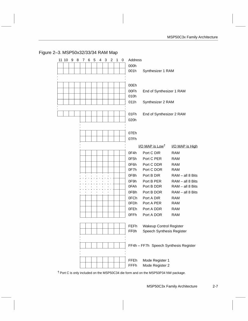
MSP50C3x Family Architecture
2-7 MSP50C3x Family Architecture
Figure 2–3. MSP50x32/33/34 RAM Map
11 10 9 8 34567 2 1 0 Address
000h001h
00Eh
00Fh010h
Synthesizer 1 RAM
Synthesizer 2 RAM
End of Synthesizer 1 RAM
01Fh
020h
End of Synthesizer 2 RAM
07Eh
07Fh
0F4h
0F5h
0F6h0F7h
0F8h
0F9h0FAh
0FBh
0FCh0FDh
0FEh
0FFh
Port C DIR
Port C PER
Port C DDRPort C DOR
Port B DIR
Port B PERPort B DDR
Port B DOR
Port A DIRPort A PER
Port A DDR
Port A DOR
RAM
RAM
RAMRAM
RAM – all 8 Bits
RAM – all 8 BitsRAM – all 8 Bits
RAM – all 8 Bits
RAMRAM
RAM
RAM
FEFhFF0h Speech Synthesis Register
Wakeup Control Register
FFEhFFFh Mode Register 2
Mode Register 1
FF4h – FF7h Speech Synthesis Register
I/O MAP is Low† I/O MAP is High
† Port C is only included on the MSP50C34 die form and on the MSP50P34 NW package.
011h
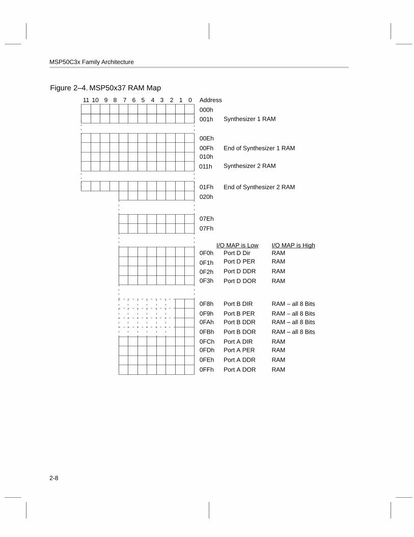
MSP50C3x Family Architecture
2-8
Figure 2–4. MSP50x37 RAM Map
11 10 9 8 34567 2 1 0 Address
000h
00Eh
00Fh010h
Synthesizer 1 RAM
Synthesizer 2 RAM
End of Synthesizer 1 RAM
01Fh
020h
End of Synthesizer 2 RAM
07Eh
07Fh
0F8h
0F9h0FAh
0FBh
0FCh0FDh
0FEh
0FFh
Port B DIR
Port B PERPort B DDR
Port B DOR
Port A DIRPort A PER
Port A DDR
Port A DOR
RAM – all 8 Bits
RAM – all 8 BitsRAM – all 8 Bits
RAM – all 8 Bits
RAMRAM
RAM
RAM
0F3h
I/O MAP is Low I/O MAP is High0F0h
0F1h
Port D Dir
0F2h
Port D PER
Port D DDR
Port D DOR
RAMRAM
RAM
RAM
001h
011h
MSP50C3x Family Architecture
2-9 MSP50C3x Family Architecture
Figure 2–4. MSP50x37 RAM Map (Continued)
FEFh
FF0h Speech Synthesis Registers
Wakeup Control Register
FFChFFDh ADC Control Register
ADC Control Register
FF7h End of Speech Synthesis Registers
FECh
FEDh
Timer Register for Long Time Measurement
FEEh
FFEhFFFh Mode Register 2
Mode Register 1
FEBh Power Amplifier Register
2.1.5 MSP50C3x Memory-Mapped Registers
Several internal registers are mapped into the RAM address space. Table 2–2shows the memory-mapped register allocations for all devices combined.
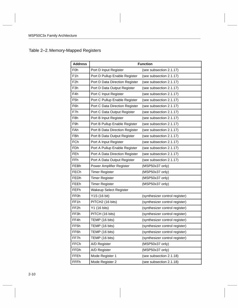
MSP50C3x Family Architecture
2-10
Table 2–2.Memory-Mapped Registers
Address Function
F0h Port D Input Register (see subsection 2.1.17)
F1h Port D Pullup Enable Register (see subsection 2.1.17)
F2h Port D Data Direction Register (see subsection 2.1.17)
F3h Port D Data Output Register (see subsection 2.1.17)
F4h Port C Input Register (see subsection 2.1.17)
F5h Port C Pullup Enable Register (see subsection 2.1.17)
F6h Port C Data Direction Register (see subsection 2.1.17)
F7h Port C Data Output Register (see subsection 2.1.17)
F8h Port B Input Register (see subsection 2.1.17)
F9h Port B Pullup Enable Register (see subsection 2.1.17)
FAh Port B Data Direction Register (see subsection 2.1.17)
FBh Port B Data Output Register (see subsection 2.1.17)
FCh Port A Input Register (see subsection 2.1.17)
FDh Port A Pullup Enable Register (see subsection 2.1.17)
FEh Port A Data Direction Register (see subsection 2.1.17)
FFh Port A Data Output Register (see subsection 2.1.17)
FEBh Power Amplifier Register (MSP50x37 only)
FECh Timer Register (MSP50x37 only)
FEDh Timer Register (MSP50x37 only)
FEEh Timer Register (MSP50x37 only)
FEFh Wakeup Select Register
FF0h Y1S (16 bit) (synthesizer control register)
FF1h PITCH2 (16 bits) (synthesizer control register)
FF2h Y1 (16 bits) (synthesizer control register)
FF3h PITCH (16 bits) (synthesizer control register)
FF4h TEMP (16 bits) (synthesizer control register)
FF5h TEMP (16 bits) (synthesizer control register)
FF6h TEMP (16 bits) (synthesizer control register)
FF7h TEMP (16 bits) (synthesizer control register)
FFCh A/D Register (MSP50x37 only)
FFDh A/D Register (MSP50x37 only)
FFEh Mode Register 1 (see subsection 2.1.18)
FFFh Mode Register 2 (see subsection 2.1.18)
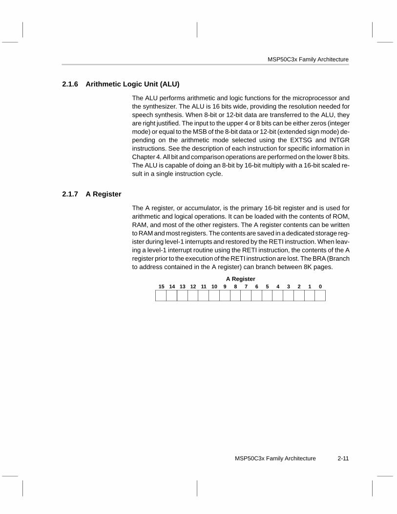
MSP50C3x Family Architecture
2-11 MSP50C3x Family Architecture
2.1.6 Arithmetic Logic Unit (ALU)
The ALU performs arithmetic and logic functions for the microprocessor andthe synthesizer. The ALU is 16 bits wide, providing the resolution needed forspeech synthesis. When 8-bit or 12-bit data are transferred to the ALU, theyare right justified. The input to the upper 4 or 8 bits can be either zeros (integermode) or equal to the MSB of the 8-bit data or 12-bit (extended sign mode) de-pending on the arithmetic mode selected using the EXTSG and INTGRinstructions. See the description of each instruction for specific information inChapter 4. All bit and comparison operations are performed on the lower 8 bits.The ALU is capable of doing an 8-bit by 16-bit multiply with a 16-bit scaled re-sult in a single instruction cycle.
2.1.7 A Register
The A register, or accumulator, is the primary 16-bit register and is used forarithmetic and logical operations. It can be loaded with the contents of ROM,RAM, and most of the other registers. The A register contents can be writtento RAM and most registers. The contents are saved in a dedicated storage reg-ister during level-1 interrupts and restored by the RETI instruction. When leav-ing a level-1 interrupt routine using the RETI instruction, the contents of the Aregister prior to the execution of the RETI instruction are lost. The BRA (Branchto address contained in the A register) can branch between 8K pages.
13 12 11 10 9 8 34567 2 1 01415A Register
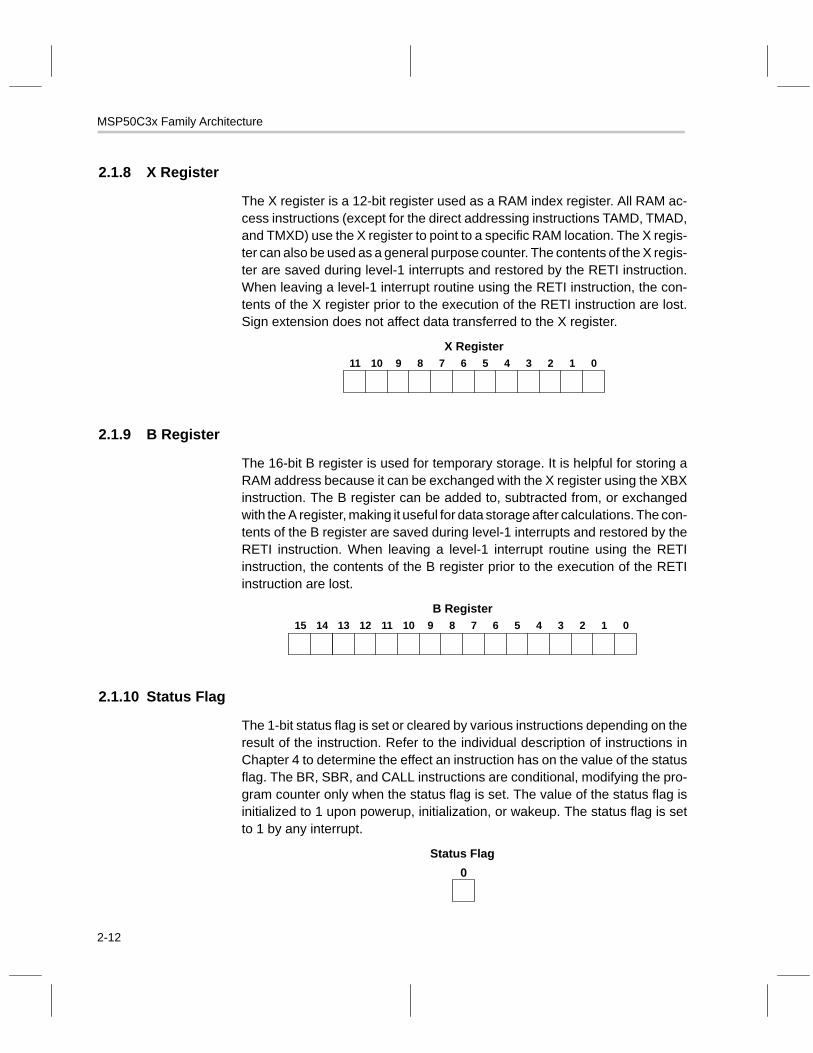
MSP50C3x Family Architecture
2-12
2.1.8 X Register
The X register is a 12-bit register used as a RAM index register. All RAM ac-cess instructions (except for the direct addressing instructions TAMD, TMAD,and TMXD) use the X register to point to a specific RAM location. The X regis-ter can also be used as a general purpose counter. The contents of the X regis-ter are saved during level-1 interrupts and restored by the RETI instruction.When leaving a level-1 interrupt routine using the RETI instruction, the con-tents of the X register prior to the execution of the RETI instruction are lost.Sign extension does not affect data transferred to the X register.
11 10 9 8 34567 2 1 0
X Register
2.1.9 B Register
The 16-bit B register is used for temporary storage. It is helpful for storing aRAM address because it can be exchanged with the X register using the XBXinstruction. The B register can be added to, subtracted from, or exchangedwith the A register, making it useful for data storage after calculations. The con-tents of the B register are saved during level-1 interrupts and restored by theRETI instruction. When leaving a level-1 interrupt routine using the RETIinstruction, the contents of the B register prior to the execution of the RETIinstruction are lost.
13 12 11 10 9 8 34567 2 1 01415
B Register
2.1.10 Status Flag
The 1-bit status flag is set or cleared by various instructions depending on theresult of the instruction. Refer to the individual description of instructions inChapter 4 to determine the effect an instruction has on the value of the statusflag. The BR, SBR, and CALL instructions are conditional, modifying the pro-gram counter only when the status flag is set. The value of the status flag isinitialized to 1 upon powerup, initialization, or wakeup. The status flag is setto 1 by any interrupt.
0
Status Flag
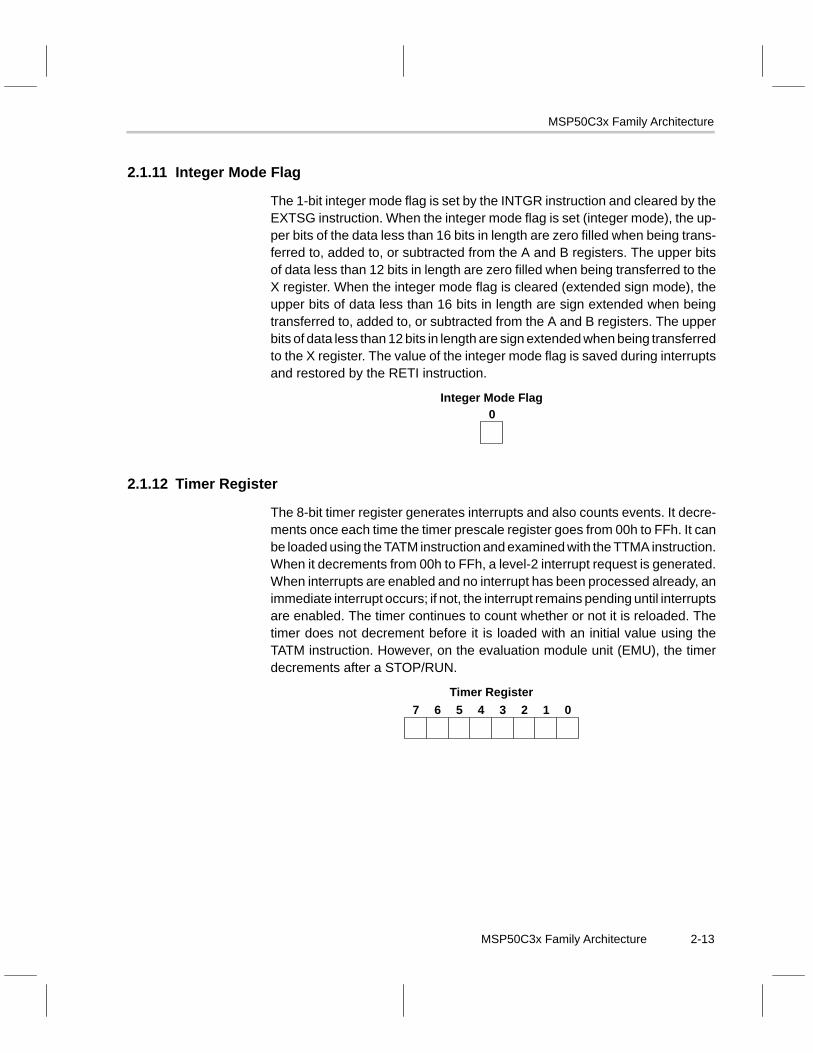
MSP50C3x Family Architecture
2-13 MSP50C3x Family Architecture
2.1.11 Integer Mode Flag
The 1-bit integer mode flag is set by the INTGR instruction and cleared by theEXTSG instruction. When the integer mode flag is set (integer mode), the up-per bits of the data less than 16 bits in length are zero filled when being trans-ferred to, added to, or subtracted from the A and B registers. The upper bitsof data less than 12 bits in length are zero filled when being transferred to theX register. When the integer mode flag is cleared (extended sign mode), theupper bits of data less than 16 bits in length are sign extended when beingtransferred to, added to, or subtracted from the A and B registers. The upperbits of data less than 12 bits in length are sign extended when being transferredto the X register. The value of the integer mode flag is saved during interruptsand restored by the RETI instruction.
0Integer Mode Flag
2.1.12 Timer Register
The 8-bit timer register generates interrupts and also counts events. It decre-ments once each time the timer prescale register goes from 00h to FFh. It canbe loaded using the TATM instruction and examined with the TTMA instruction.When it decrements from 00h to FFh, a level-2 interrupt request is generated.When interrupts are enabled and no interrupt has been processed already, animmediate interrupt occurs; if not, the interrupt remains pending until interruptsare enabled. The timer continues to count whether or not it is reloaded. Thetimer does not decrement before it is loaded with an initial value using theTATM instruction. However, on the evaluation module unit (EMU), the timerdecrements after a STOP/RUN.
34567 2 1 0
Timer Register
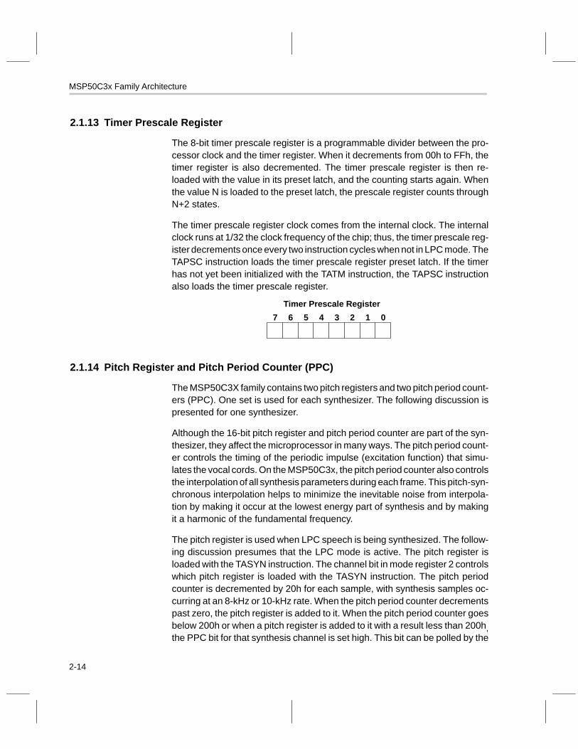
MSP50C3x Family Architecture
2-14
2.1.13 Timer Prescale Register
The 8-bit timer prescale register is a programmable divider between the pro-cessor clock and the timer register. When it decrements from 00h to FFh, thetimer register is also decremented. The timer prescale register is then re-loaded with the value in its preset latch, and the counting starts again. Whenthe value N is loaded to the preset latch, the prescale register counts throughN+2 states.
The timer prescale register clock comes from the internal clock. The internalclock runs at 1/32 the clock frequency of the chip; thus, the timer prescale reg-ister decrements once every two instruction cycles when not in LPC mode. TheTAPSC instruction loads the timer prescale register preset latch. If the timerhas not yet been initialized with the TATM instruction, the TAPSC instructionalso loads the timer prescale register.
34567 2 1 0
Timer Prescale Register
2.1.14 Pitch Register and Pitch Period Counter (PPC)
The MSP50C3X family contains two pitch registers and two pitch period count-ers (PPC). One set is used for each synthesizer. The following discussion ispresented for one synthesizer.
Although the 16-bit pitch register and pitch period counter are part of the syn-thesizer, they affect the microprocessor in many ways. The pitch period count-er controls the timing of the periodic impulse (excitation function) that simu-lates the vocal cords. On the MSP50C3x, the pitch period counter also controlsthe interpolation of all synthesis parameters during each frame. This pitch-syn-chronous interpolation helps to minimize the inevitable noise from interpola-tion by making it occur at the lowest energy part of synthesis and by makingit a harmonic of the fundamental frequency.
The pitch register is used when LPC speech is being synthesized. The follow-ing discussion presumes that the LPC mode is active. The pitch register isloaded with the TASYN instruction. The channel bit in mode register 2 controlswhich pitch register is loaded with the TASYN instruction. The pitch periodcounter is decremented by 20h for each sample, with synthesis samples oc-curring at an 8-kHz or 10-kHz rate. When the pitch period counter decrementspast zero, the pitch register is added to it. When the pitch period counter goesbelow 200h or when a pitch register is added to it with a result less than 200h,the PPC bit for that synthesis channel is set high. This bit can be polled by the
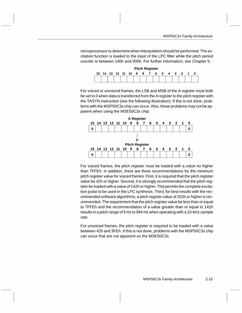
MSP50C3x Family Architecture
2-15 MSP50C3x Family Architecture
microprocessor to determine when interpolation should be performed. The ex-citation function is loaded to the input of the LPC filter while the pitch periodcounter is between 140h and 000h. For further information, see Chapter 5.
13 12 11 10 9 8 34567 2 1 01415
Pitch Register
For voiced or unvoiced frames, the LSB and MSB of the A register must bothbe set to 0 when data is transferred from the A register to the pitch register withthe TASYN instruction (see the following illustration). If this is not done, prob-lems with the MSP50C3x chip can occur. Also, these problems may not be ap-parent when using the MSE50C3x chip.
13 12 11 10 9 8 34567 2 1 0
0
A Register
13 12 11 10 9 8 34567 2 1 0
0
Pitch Register
15
0
14
15
0
14
For voiced frames, the pitch register must be loaded with a value no higherthan 7FFEh. In addition, there are three recommendations for the minimumpitch register value for voiced frames. First, it is required that the pitch registervalue be 42h or higher. Second, it is strongly recommended that the pitch reg-ister be loaded with a value of 142h or higher. This permits the complete excita-tion pulse to be used in the LPC synthesis. Third, for best results with the rec-ommended software algorithms, a pitch register value of 202h or higher is rec-ommended. The requirement that the pitch register value be less than or equalto 7FFEh and the recommendation of a value greater than or equal to 142hresults in a pitch range of 9 Hz to 994 Hz when operating with a 10-kHz samplerate.
For unvoiced frames, the pitch register is required to be loaded with a valuebetween 42h and 3FEh. If this is not done, problems with the MSP50C3x chipcan occur that are not apparent on the MSE50C3x.
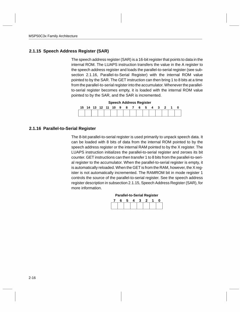
MSP50C3x Family Architecture
2-16
2.1.15 Speech Address Register (SAR)
The speech address register (SAR) is a 16-bit register that points to data in theinternal ROM. The LUAPS instruction transfers the value in the A register tothe speech address register and loads the parallel-to-serial register (see sub-section 2.1.16, Parallel-to-Serial Register) with the internal ROM valuepointed to by the SAR. The GET instruction can then bring 1 to 8 bits at a timefrom the parallel-to-serial register into the accumulator. Whenever the parallel-to-serial register becomes empty, it is loaded with the internal ROM valuepointed to by the SAR, and the SAR is incremented.
13 12 11 10 9 8 34567 2 1 01415
Speech Address Register
2.1.16 Parallel-to-Serial Register
The 8-bit parallel-to-serial register is used primarily to unpack speech data. Itcan be loaded with 8 bits of data from the internal ROM pointed to by thespeech address register or the internal RAM pointed to by the X register. TheLUAPS instruction initializes the parallel-to-serial register and zeroes its bitcounter. GET instructions can then transfer 1 to 8 bits from the parallel-to-seri-al register to the accumulator. When the parallel-to-serial register is empty, itis automatically reloaded. When the GET is from the RAM, however, the X reg-ister is not automatically incremented. The RAMROM bit in mode register 1controls the source of the parallel-to-serial register. See the speech addressregister description in subsection 2.1.15, Speech Address Register (SAR), formore information.
34567 2 1 0
Parallel-to-Serial Register
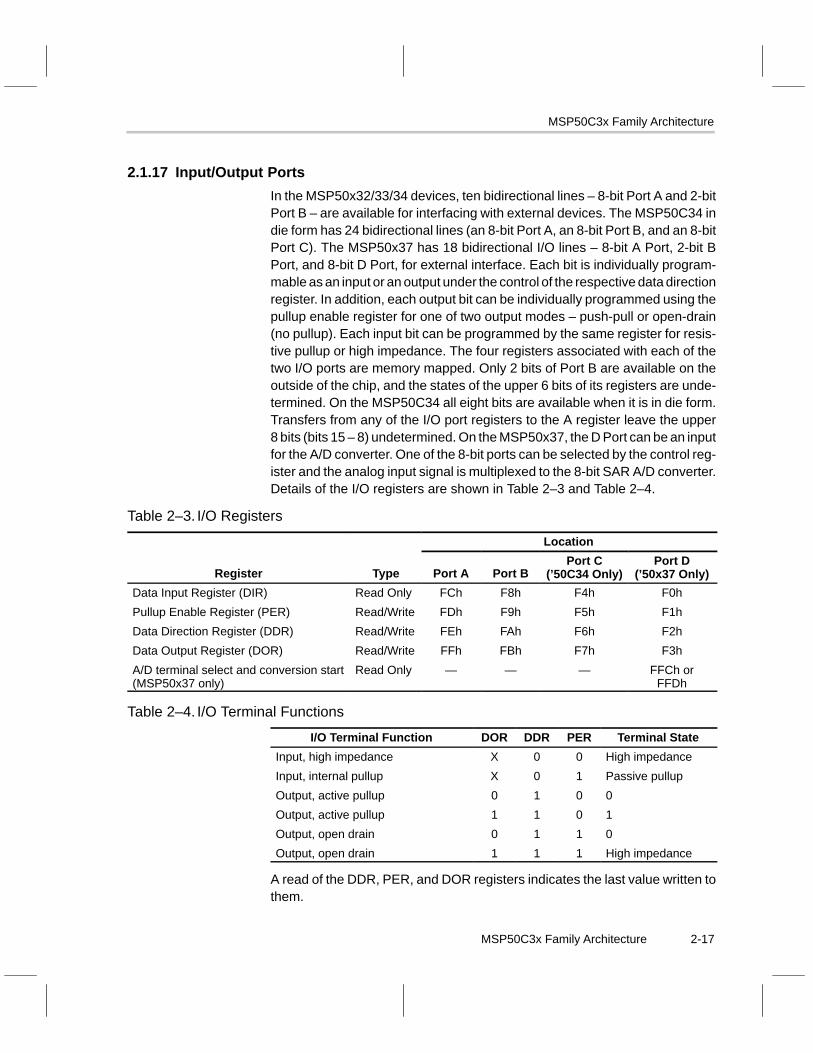
MSP50C3x Family Architecture
2-17 MSP50C3x Family Architecture
2.1.17 Input/Output Ports
In the MSP50x32/33/34 devices, ten bidirectional lines – 8-bit Port A and 2-bitPort B – are available for interfacing with external devices. The MSP50C34 indie form has 24 bidirectional lines (an 8-bit Port A, an 8-bit Port B, and an 8-bitPort C). The MSP50x37 has 18 bidirectional I/O lines – 8-bit A Port, 2-bit BPort, and 8-bit D Port, for external interface. Each bit is individually program-mable as an input or an output under the control of the respective data directionregister. In addition, each output bit can be individually programmed using thepullup enable register for one of two output modes – push-pull or open-drain(no pullup). Each input bit can be programmed by the same register for resis-tive pullup or high impedance. The four registers associated with each of thetwo I/O ports are memory mapped. Only 2 bits of Port B are available on theoutside of the chip, and the states of the upper 6 bits of its registers are unde-termined. On the MSP50C34 all eight bits are available when it is in die form.Transfers from any of the I/O port registers to the A register leave the upper8 bits (bits 15 – 8) undetermined. On the MSP50x37, the D Port can be an inputfor the A/D converter. One of the 8-bit ports can be selected by the control reg-ister and the analog input signal is multiplexed to the 8-bit SAR A/D converter.Details of the I/O registers are shown in Table 2–3 and Table 2–4.
Table 2–3. I/O Registers
Location
Register Type Port A Port BPort C
(’50C34 Only)Port D
(’50x37 Only)
Data Input Register (DIR) Read Only FCh F8h F4h F0h
Pullup Enable Register (PER) Read/Write FDh F9h F5h F1h
Data Direction Register (DDR) Read/Write FEh FAh F6h F2h
Data Output Register (DOR) Read/Write FFh FBh F7h F3h
A/D terminal select and conversion start(MSP50x37 only)
Read Only — — — FFCh orFFDh
Table 2–4. I/O Terminal Functions
I/O Terminal Function DOR DDR PER Terminal State
Input, high impedance X 0 0 High impedance
Input, internal pullup X 0 1 Passive pullup
Output, active pullup 0 1 0 0
Output, active pullup 1 1 0 1
Output, open drain 0 1 1 0
Output, open drain 1 1 1 High impedance
A read of the DDR, PER, and DOR registers indicates the last value written tothem.
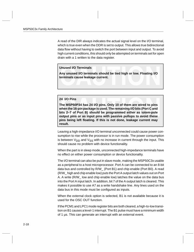
MSP50C3x Family Architecture
2-18
A read of the DIR always indicates the actual signal level on the I/O terminal,which is true even when the DDR is set to output. This allows true bidirectionaldata flow without having to switch the port between input and output. To avoidhigh current conditions, this should only be attempted on terminals set for opendrain with a 1 written to the data register.
Unused I/O Terminals
Any unused I/O terminals should be tied high or low. Floating I/Oterminals cause leakage current.
24 I/O Pins
The MSP50P34 has 24 I/O pins. Only 10 of them are wired to pinswhen the 16-pin package is used. The remaining I/O bits (Port C andbits 2–7 of Port B) should be programmed either as totem-poleoutput pins or as input pins with passive pullups to avoid thesepins being left floating. If this is not done, leakage current mayresult.
Leaving a high-impedance I/O terminal unconnected could cause power con-sumption to rise while the processor is in run mode. The power consumptionis between VDD and VSS with no increase in current through the input. Thisshould cause no problem with device functionality.
When the part is in sleep mode, unconnected high-impedance terminals haveno effect on either power consumption or device functionality.
The I/O terminal can also be put in slave mode, making the MSP50C3x usableas a peripheral to a host microprocessor. Port A can be connected to an 8-bitdata bus and controlled by R/W_ (Port B1) and chip enable (Port B0). A read(R/W_ high and chip enable low) puts the Port A output latch values out on PortA. A write (R/W_ low and chip enable low) latches the value on the data businto the Port A input latch. In addition, bit 7 of the A output latch is cleared. Thismakes it possible to use A7 as a write handshake line. Any lines used on thedata bus in this mode must be configured as inputs.
When the external clock option is selected, B1 is not available because it isused for the OSC OUT function.
If the PCM1 and LPC1 mode register bits are both cleared, a high-to-low transi-tion on B1 causes a level-1 interrupt. The B1 pulse must have a minimum widthof 1 µs. This can generate an interrupt with an external event.
MSP50C3x Family Architecture
2-19 MSP50C3x Family Architecture
2.1.18 Mode Registers
There are two 8-bit mode registers that are memory mapped. The contents ofboth mode register 1 is cleared to 0 upon power-up reset, wakeup, or whenthe INIT line pulses low. The contents of the mode register 2 is initialized to 09h(PPC bits are both high) upon INIT. The contents of the two mode registers arenot saved during a subroutine call or interrupt.
Mode register 1 is memory mapped to RAM address FFEh and mode register2 is memory mapped to RAM address FFFh. The contents of either mode reg-ister can be copied to the A register using the TMA instruction. Individual bitsof either mode register can be tested using the TSTCM instruction or modifiedusing the ANDCM and ORCM instructions. The TAMODE instruction transfersthe bottom 8 bits of the A register to mode register 1.
2.1.18.1 Mode Register 1
The usage of the mode register 1 bits are given in Table 2–5. Mode register1 controls the first synthesizer channel, the interrupt mode, the slave mode,and the GET mode.
The ENA1 and ENA2 bits in the mode register enable or disable the level-1 andlevel-2 interrupts respectively. If an interrupt condition occurs while the corre-sponding ENA1 or ENA2 bit in the mode register is cleared to 0, an interruptpending latch is set, and the execution of the interrupt is delayed until the inter-rupt is enabled.
The LPC1, PCM1, and UNVOICE1 bits control the activity of the first synthesischannel. See Section 2.2, Speech Synthesis, for more information. The LPC1and PCM1 bits control the interrupt vectors.
Note: Using the ORCM Instruction
When using the ORCM instruction on the UNVOICE1 bit, the LPC1 bit shouldalso be reset to avoid a glitch in the LPC (i.e., ORCM UNV + LPC1).
The SLAVE bit enables a special I/O mode designed to enable the MSP50C3xto operate as a slave processor under the control of an external master micro-processor. See Chapter 5, Applications, for more information.
The RAMROM bit selects the data source for GET instructions. When RAM-ROM is low, the GET instruction accesses the internal ROM. When the RAM-ROM bit is set high, the GET instruction accesses the RAM location selectedby the X register.
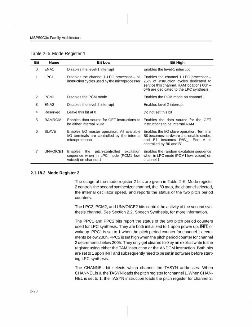
MSP50C3x Family Architecture
2-20
Table 2–5.Mode Register 1
Bit Name Bit Low Bit High
0 ENA1 Disables the level-1 interrupt Enables the level-1 interrupt
1 LPC1 Disables the channel 1 LPC processor – allinstruction cycles used by the microprocessor
Enables the channel 1 LPC processor –25% of instruction cycles dedicated toservice this channel. RAM locations 00h –0Fh are dedicated to the LPC synthesis.
2 PCM1 Disables the PCM mode Enables the PCM mode on channel 1
3 ENA2 Disables the level-2 interrupt Enables level-2 interrupt
4 Reserved Leave this bit at 0 Do not set this bit
5 RAMROM Enables data source for GET instructions tobe either internal ROM
Enables the data source for the GETinstructions to be internal RAM
6 SLAVE Enables I/O master operation. All availableI/O terminals are controlled by the internalmicroprocessor
Enables the I/O slave operation. TerminalB0 becomes hardware chip enable strobe,and B1 becomes R/W_, Port A iscontrolled by B0 and B1
7 UNVOICE1 Enables the pitch-controlled excitationsequence when in LPC mode (PCM1 low,voiced) on channel 1
Enables the random excitation sequencewhen in LPC mode (PCM1 low, voiced) onchannel 1
2.1.18.2 Mode Register 2
The usage of the mode register 2 bits are given in Table 2–6. Mode register2 controls the second synthesizer channel, the I/O map, the channel selected,the internal oscillator speed, and reports the status of the two pitch periodcounters.
The LPC2, PCM2, and UNVOICE2 bits control the activity of the second syn-thesis channel. See Section 2.2, Speech Synthesis, for more information.
The PPC1 and PPC2 bits report the status of the two pitch period countersused for LPC synthesis. They are both initialized to 1 upon power up, INIT, orwakeup. PPC1 is set to 1 when the pitch period counter for channel 1 decre-ments below 200h. PPC2 is set high when the pitch period counter for channel2 decrements below 200h. They only get cleared to 0 by an explicit write to theregister using either the TAM instruction or the ANDCM instruction. Both bitsare set to 1 upon INIT and subsequently need to be set in software before start-ing LPC synthesis.
The CHANNEL bit selects which channel the TASYN addresses. WhenCHANNEL is 0, the TASYN loads the pitch register for channel 1. When CHAN-NEL is set to 1, the TASYN instruction loads the pitch register for channel 2.
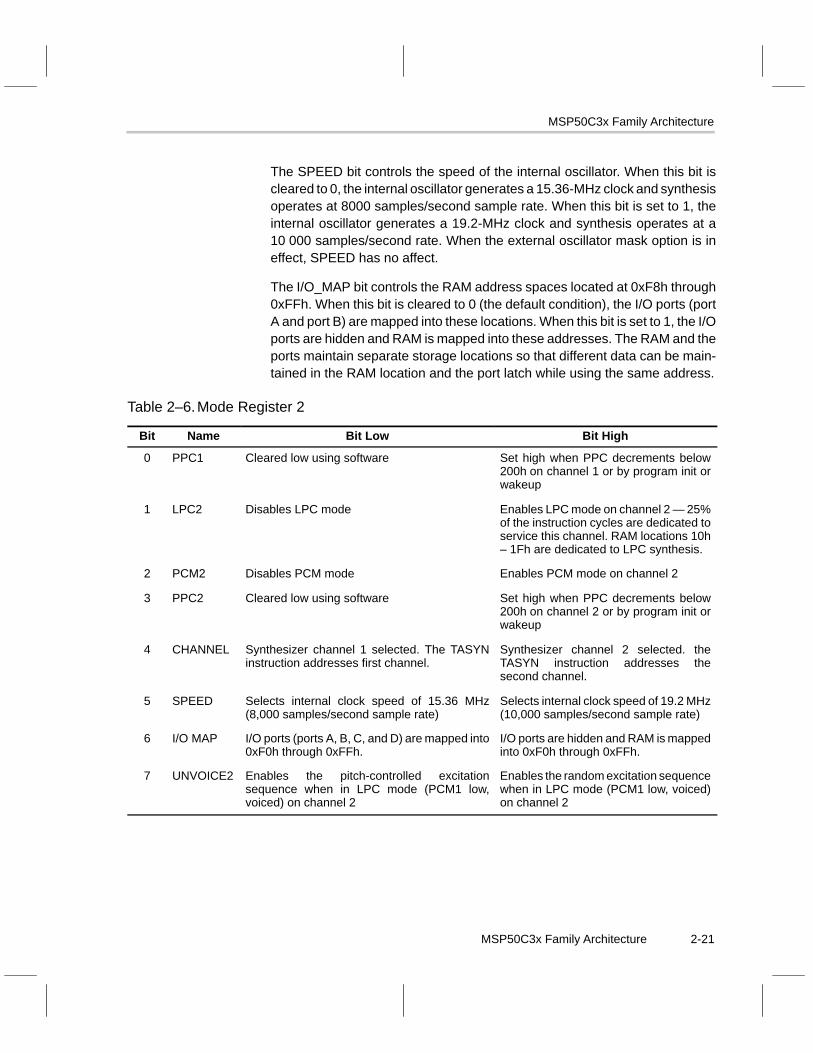
MSP50C3x Family Architecture
2-21 MSP50C3x Family Architecture
The SPEED bit controls the speed of the internal oscillator. When this bit iscleared to 0, the internal oscillator generates a 15.36-MHz clock and synthesisoperates at 8000 samples/second sample rate. When this bit is set to 1, theinternal oscillator generates a 19.2-MHz clock and synthesis operates at a10 000 samples/second rate. When the external oscillator mask option is ineffect, SPEED has no affect.
The I/O_MAP bit controls the RAM address spaces located at 0xF8h through0xFFh. When this bit is cleared to 0 (the default condition), the I/O ports (portA and port B) are mapped into these locations. When this bit is set to 1, the I/Oports are hidden and RAM is mapped into these addresses. The RAM and theports maintain separate storage locations so that different data can be main-tained in the RAM location and the port latch while using the same address.
Table 2–6.Mode Register 2
Bit Name Bit Low Bit High
0 PPC1 Cleared low using software Set high when PPC decrements below200h on channel 1 or by program init orwakeup
1 LPC2 Disables LPC mode Enables LPC mode on channel 2 — 25%of the instruction cycles are dedicated toservice this channel. RAM locations 10h– 1Fh are dedicated to LPC synthesis.
2 PCM2 Disables PCM mode Enables PCM mode on channel 2
3 PPC2 Cleared low using software Set high when PPC decrements below200h on channel 2 or by program init orwakeup
4 CHANNEL Synthesizer channel 1 selected. The TASYNinstruction addresses first channel.
Synthesizer channel 2 selected. theTASYN instruction addresses thesecond channel.
5 SPEED Selects internal clock speed of 15.36 MHz(8,000 samples/second sample rate)
Selects internal clock speed of 19.2 MHz(10,000 samples/second sample rate)
6 I/O MAP I/O ports (ports A, B, C, and D) are mapped into0xF0h through 0xFFh.
I/O ports are hidden and RAM is mappedinto 0xF0h through 0xFFh.
7 UNVOICE2 Enables the pitch-controlled excitationsequence when in LPC mode (PCM1 low,voiced) on channel 2
Enables the random excitation sequencewhen in LPC mode (PCM1 low, voiced)on channel 2

Speech Synthesis
2-22
2.2 Speech Synthesis
The MSP50C3x family incorporates two synthesis channels. Each synthesischannel can be controlled separately by setting or clearing bits in the two moderegisters, loading one or both of the pitch registers using the TASYN instruc-tion, and by properly loading values to the synthesis RAM. The output of eachchannel is added together at the input of the oversampling output filter. Eachsynthesis channel can operate in one of four modes based upon the settingof the LPCx and PCMx bits in the mode register. In the following discussion,LPCx refers to either the LPC1 or the LPC2 bit in the mode register dependingupon which synthesis channel is active. In a similar manner, PCMx , UNVOI-CEx, and PPCx refer to PCM1, PCM2, UNVOICE1, UNVOICE2, PPC1, andPPC2 depending upon context.
2.2.1 Synthesizer Mode 0 – Off
When the PCMx and LPCx bits are both cleared, the synthesizer channel isdisabled. No microprocessor cycles are needed to service a channel in thismode. The TASYN instruction transfers the contents of the A register to thepitch register selected by the CHANNEL bit in mode register 2, making it easyto preload the pitch register prior to starting the LPC synthesizer. If the LPC1and PCM1 bits in mode register 1 are both cleared to 0, the level-1 interruptis triggered by a high-to-low transition on terminal B1 and the DAC is disabled.
2.2.2 Synthesizer Mode 1 – LPC
Synthesizer mode 1 is the normal speaking mode. It is selected by setting theLPCx bit to 1 and clearing the PCMx bit to 0. In this mode, the TASYN instruc-tion transfers the contents of the A register to the pitch register selected by theCHANNEL bit in mode register 2. If synthesis channel 1 is in this mode, thelevel-1 interrupt occurs synchronously with the filter speech sample rate.Approximately 25 percent of the instruction cycles are used by each synthesischannel using this mode.
The PPCx bit in mode register 2 is set to 1 when the pitch period counter forthat channel decrements below 200h or when the pitch register is added to thepitch period counter with a result less than 200h. The PPCx bit in mode register2 remains at 1 until reset to 0 by the software.
The microprocessor controls speech synthesis by unpacking and decodingparameters, setting the update interval (frame rate), and interpolating the pa-rameters during the frame. The speech synthesizer acts as a 12-pole digitallattice filter, a pitch-controlled or white-noise excitation generator, a 2-pole dig-ital low-pass filter, and a digital-to-analog converter (DAC). Speech parameter
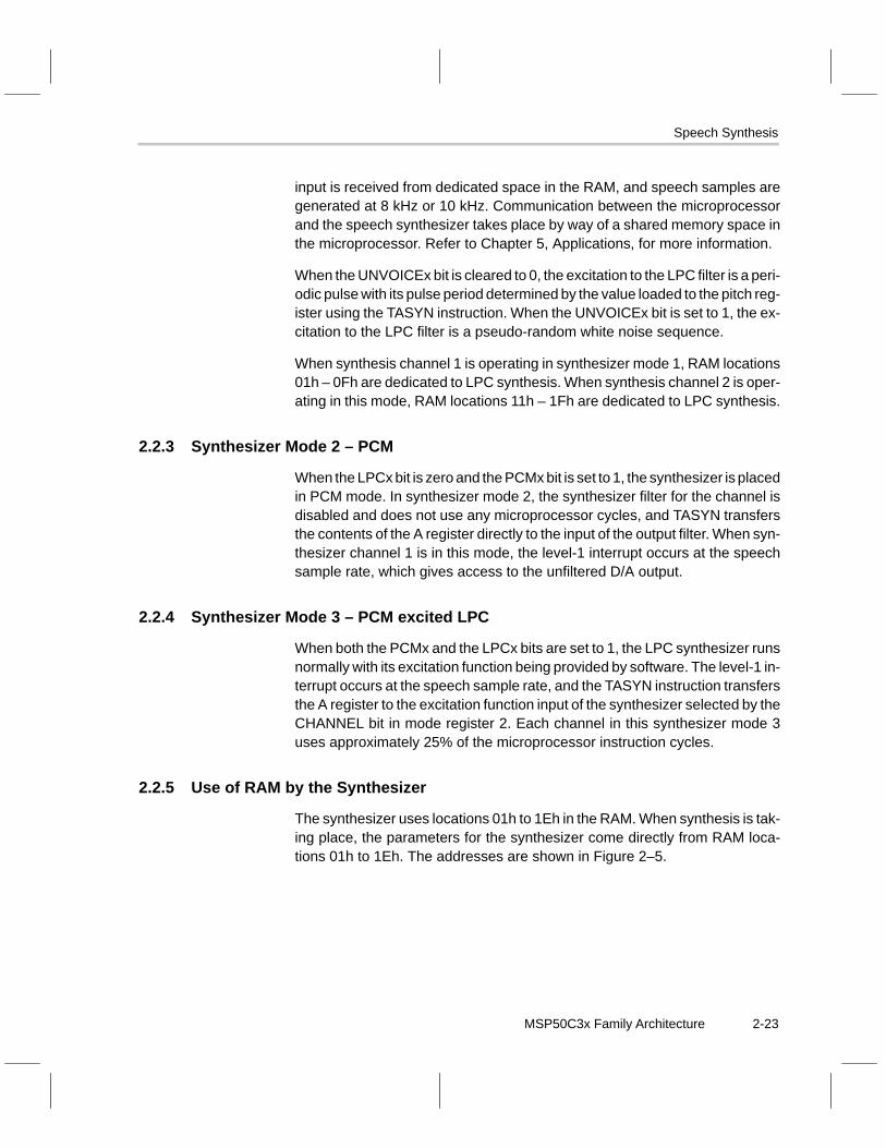
Speech Synthesis
2-23 MSP50C3x Family Architecture
input is received from dedicated space in the RAM, and speech samples aregenerated at 8 kHz or 10 kHz. Communication between the microprocessorand the speech synthesizer takes place by way of a shared memory space inthe microprocessor. Refer to Chapter 5, Applications, for more information.
When the UNVOICEx bit is cleared to 0, the excitation to the LPC filter is a peri-odic pulse with its pulse period determined by the value loaded to the pitch reg-ister using the TASYN instruction. When the UNVOICEx bit is set to 1, the ex-citation to the LPC filter is a pseudo-random white noise sequence.
When synthesis channel 1 is operating in synthesizer mode 1, RAM locations01h – 0Fh are dedicated to LPC synthesis. When synthesis channel 2 is oper-ating in this mode, RAM locations 11h – 1Fh are dedicated to LPC synthesis.
2.2.3 Synthesizer Mode 2 – PCM
When the LPCx bit is zero and the PCMx bit is set to 1, the synthesizer is placedin PCM mode. In synthesizer mode 2, the synthesizer filter for the channel isdisabled and does not use any microprocessor cycles, and TASYN transfersthe contents of the A register directly to the input of the output filter. When syn-thesizer channel 1 is in this mode, the level-1 interrupt occurs at the speechsample rate, which gives access to the unfiltered D/A output.
2.2.4 Synthesizer Mode 3 – PCM excited LPC
When both the PCMx and the LPCx bits are set to 1, the LPC synthesizer runsnormally with its excitation function being provided by software. The level-1 in-terrupt occurs at the speech sample rate, and the TASYN instruction transfersthe A register to the excitation function input of the synthesizer selected by theCHANNEL bit in mode register 2. Each channel in this synthesizer mode 3uses approximately 25% of the microprocessor instruction cycles.
2.2.5 Use of RAM by the Synthesizer
The synthesizer uses locations 01h to 1Eh in the RAM. When synthesis is tak-ing place, the parameters for the synthesizer come directly from RAM loca-tions 01h to 1Eh. The addresses are shown in Figure 2–5.
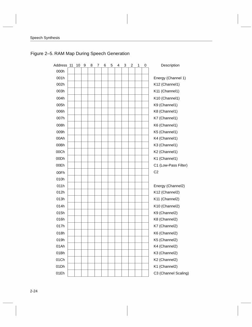
Speech Synthesis
2-24
Figure 2–5. RAM Map During Speech Generation
34567 2 1 0 Description
Energy (Channel 1)
K12 (Channel1)
K11 (Channel1)
K10 (Channel1)
K9 (Channel1)
K8 (Channel1)
K7 (Channel1)
K6 (Channel1)
K5 (Channel1)
K4 (Channel1)
K3 (Channel1)
K1 (Channel1)
C1 (Low-Pass Filter)
K2 (Channel1)
C2
9 8Address
000h
001h
002h
003h
004h
005h
006h
007h
008h
009h
00Ah
00Bh
00Dh
00Eh
00Ch
00Fh
1011
Energy (Channel2)
K12 (Channel2)
K11 (Channel2)
K10 (Channel2)
K9 (Channel2)
K8 (Channel2)
K7 (Channel2)
K6 (Channel2)
K5 (Channel2)
K4 (Channel2)
K3 (Channel2)
K1 (Channel2)
C3 (Channel Scaling)
K2 (Channel2)
010h
011h
012h
013h
014h
015h
016h
017h
018h
019h
01Ah
01Bh
01Dh
01Eh
01Ch
Speech Synthesis
2-25 MSP50C3x Family Architecture
2.2.6 Low Pass Filter
The MSP50C3x synthesizer incorporates an oversampling output filter. Itsflow diagram is shown in Figure 2–6. The output of the LPC filter (appropriatelydelayed) is alternately switched with the output of a FIR filter as shown at a ratedouble the speech sample rate. With the appropriate choice of parameters (C1and C2), this filter interpolates data points and improves sound quality. Rec-ommended values are C1 = F61h and C2 = B67h or C1 = E00h and C2 = A00h.
Figure 2–6. Oversampling Output Filter
Z –1Z –1
C1
Z –110 kHz
C2 C2 C1
SN SN–1 SN–2 SN–3
+LATCH
PWMD/A
LPC-12Lattice Filter
20 kHz
φ
FIRn
2.2.7 Channel Scaling (C3)
When both LPC channels are operating, the channel 2 output is scaled relativeto the channel 1 output by the value loaded to RAM location 1Eh. When it isdesired that both channels operate with the same scaling, load RAM location1Eh with the value 7FFh. Loading values smaller than this linearly scale theoutput of channel 2 with respect to channel 1.
Speech Synthesis
2-26
2.2.8 Frame Length Control
The frame length is controlled by the value put into the prescale register andthe range over which the timer is allowed to vary. Typical synthesis and inter-polation routines let the timer decrement through a range of fixed size. Conse-quently, the prescale value should be selected to give the proper frame dura-tion based on the timer range.
2.2.9 Digital-to-Analog Converter
The MSP50C3x contains an internal digital-to-analog converter (DAC) con-nected to the output of the synthesizer. The DAC is available in two pulse-den-sity-modulated forms. See Section 1.5, D/A Options, for more information. TheDAC output produces samples at a rate given by fosc/1920. For a 19.2-MHzclock frequency, this formula results in an output sample rate of 20 KHz. Fora 15.36-MHz clock frequency, this results in an output sample rate of 16 KHz.The DAC output rate is twice the speech sample rate with a digital low-passfilter in all modes except PCM mode. When the synthesizer is off (mode 0), theDAC goes to an off state. The off state is the same as a zero state.
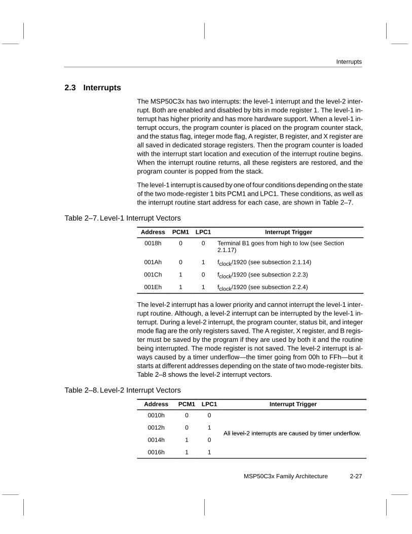
Interrupts
2-27 MSP50C3x Family Architecture
2.3 Interrupts
The MSP50C3x has two interrupts: the level-1 interrupt and the level-2 inter-rupt. Both are enabled and disabled by bits in mode register 1. The level-1 in-terrupt has higher priority and has more hardware support. When a level-1 in-terrupt occurs, the program counter is placed on the program counter stack,and the status flag, integer mode flag, A register, B register, and X register areall saved in dedicated storage registers. Then the program counter is loadedwith the interrupt start location and execution of the interrupt routine begins.When the interrupt routine returns, all these registers are restored, and theprogram counter is popped from the stack.
The level-1 interrupt is caused by one of four conditions depending on the stateof the two mode-register 1 bits PCM1 and LPC1. These conditions, as well asthe interrupt routine start address for each case, are shown in Table 2–7.
Table 2–7.Level-1 Interrupt Vectors
Address PCM1 LPC1 Interrupt Trigger
0018h 0 0 Terminal B1 goes from high to low (see Section2.1.17)
001Ah 0 1 fclock/1920 (see subsection 2.1.14)
001Ch 1 0 fclock/1920 (see subsection 2.2.3)
001Eh 1 1 fclock/1920 (see subsection 2.2.4)
The level-2 interrupt has a lower priority and cannot interrupt the level-1 inter-rupt routine. Although, a level-2 interrupt can be interrupted by the level-1 in-terrupt. During a level-2 interrupt, the program counter, status bit, and integermode flag are the only registers saved. The A register, X register, and B regis-ter must be saved by the program if they are used by both it and the routinebeing interrupted. The mode register is not saved. The level-2 interrupt is al-ways caused by a timer underflow—the timer going from 00h to FFh—but itstarts at different addresses depending on the state of two mode-register bits.Table 2–8 shows the level-2 interrupt vectors.
Table 2–8.Level-2 Interrupt Vectors
Address PCM1 LPC1 Interrupt Trigger
0010h 0 0
0012h 0 1All level-2 interrupts are caused by timer underflow
0014h 1 0All level-2 interru ts are caused by timer underflow.
0016h 1 1
Interrupts
2-28
The interrupting conditions for the level-1 and level-2 interrupt set interrupt-pending latches. When an interrupt is enabled (and in the level-2 interruptcase, not overridden by a level-1 interrupt pending condition), the interrupt istaken immediately. If, however, the interrupt is not enabled, the interrupt pend-ing latch causes an interrupt to occur as soon as the respective interrupt is en-abled in mode register 1.
Interrupts are not taken in the middle of double-byte instructions, duringbranch or call instructions, or during the subroutine or interrupt returns (RETNor RETI). A single instruction software loop (instruction of BR, BRA, CALL, orSBR to itself) should be avoided since an interrupt is never taken. Consecu-tively executed branches or calls delay interrupts until after the execution ofthe instruction at the eventual destination of the string of branches (or calls).
If consecutive branches (or calls) are avoided, the worst-case interrupt delayin the main level is four instruction cycles. The worst-case delay occurs whenthe interrupt occurs during the first execution cycle of a branch and the firstinstruction at the branch destination address is a double-cycle instruction.
When the interrupt occurs, execution begins at the interrupt address. The stateof the status bit is not known when the interrupt occurs, so a BR or CALLinstruction should not be used for the first instruction. Two SBRs can be used,since one of them is always taken, or it may be possible to use some otherinstruction that sets the status bit, followed by an SBR.
The mode register is not saved and restored during interrupts. Any changesmade to the mode register during interrupts remain in effect after the return,including the enabling and disabling of interrupts.
MSP50C3x Power Control and Initialization
2-29 MSP50C3x Family Architecture
2.4 MSP50C3x Power Control and Initialization
Upon initial powerup, the status bit is set to 1, the sign extension is set to inte-ger mode, the RAM contents are unknown, and the I/O RAM is cleared to all0s, forcing the I/O terminals to a high-impedance input state. Mode Register 1is initialized to 0, and Mode Register 2 is initialized to 09h. The software pro-gram begins operating at ROM location 0000. The device may subsequentlybe placed in one of several power saving modes:
STANDBY
Executing a SETOFF instruction places the device in a standby mode.When this occurs, the internal clock is shut down, the program stopsexecuting, and the device is placed in a low-power state. The I/O lines re-tain their last programmed state.
This mode can be terminated either by taking INIT low or by waking thedevice with a negative transition on a designated wakeup line. Any A Portline can be software selected as a wakeup line. This is done by setting thecorresponding bit in the Wakeup Control Register (FEFh). When the de-vice is restarted using a wakeup line, the program begins executing atROM location 0002.
When the device is restarted, the RAM is retained, the mode registers arecleared to 0, the I/O lines are unchanged, the status bit is set to 1, and therandom number counter is unchanged. The device is otherwisecompletely initialized.
TSP50C1x Device Family
The TSP50C1x device family set the I/O to a high impedance inputstate after a SETOFF command. This is not true in the MSP50x3xfamily. The I/O is left in its last programmed state.
Additional Precautions
The MSP50P34 requires additional precautions when placing thedevice into the standby condition which are not required on theother MSP50C3x device family. If B0 is programmed as an input,than it should be driven either high or low. In addition, the I/O portsB2..B7 and C0..C7 exist on the MSP50P34 and will not be bondedout in the 16-pin package. Software should program these I/O portsto an output state. If these precautions are not taken, some leakagecurrent may result.
MSP50C3x Clocks
2-30
SLEEP
Taking the INIT line low reinitializes the MSP50C3x and places the devicein a sleep mode. The program counter is cleared to 0000, the randomnumber counter is reinitialized, the I/O lines are set to a high-impedancestate, and the state of the device is completely initialized. When the INITsignal returns high, the program begins executing at ROM location 0000with the status bit set to 1.
2.5 MSP50C3x Clocks
The MSP50C3x can operate either off an internal clock requiring no externalcomponents or off an external clock requiring external components. Either theinternal clock or the external clock can be selected as a mask option when thedevice code is released. The internal clock is used when economy is more im-portant than absolute frequency accuracy. The external clock is used when thefrequency accuracy requirements of the clock justify the added cost of the nec-essary external components, when the preset frequencies available with theinternal clock are not applicable to the application, or when synchronizationwith other processors is important.
2.5.1 Internal Oscillator
The internal clock provides either 15.36 MHz or 19.2 MHz selectable by settingor clearing the SPEED bit in mode register 2. Both frequencies are trimmedduring the manufacturing process. When using the internal clock, OSC INshould be tied to VSS. The internal clock is disabled when either INIT is takenlow or when a SETOFF instruction is executed. It is enabled when the INIT re-turns high or when a device wakeup occurs.
2.5.2 External Oscillator
The external oscillator provides the capability of providing either nonstandardor more accurate clock frequencies. Using the on-chip oscillator, either a ce-ramic resonator or a quartz crystal can be connected between OSC IN and theOSC OUT to provide a custom frequency. Alternatively, OSC IN can be drivenwith an externally derived clock signal. The on-chip oscillator circuit is disabledwhen the MSP50C3x is placed in any low-power mode. When the external os-cillator mask option is selected, Port B1 is not available since an extra terminalis required to provide the oscillator output line (OSC OUT). See Figure 1–16for a suggested external oscillator circuit.
2.5.3 External Clock
The external clock mask option allows an externally derived clock to be usedby the device without loosing the Port B1 terminal. It is identical to the externaloscillator except that terminal 7 is used for Port B1 and an oscillator return lineis not provided.
MSP50C3x Clocks
2-31 MSP50C3x Family Architecture
2.5.4 Long Interval Monitor Timer – Timer-2 (MSP50x37 Only)
The MSP50x37 implements a set of timers in addition to timers incorporatedin the CPU. Since this timer is designed for long interval time count, such asthat required for external host processor communication, this timer does notinitiate any interrupt. Table 2–9 shows the memory map of this timer.
Note: Long Interval Timer
The long interval timer does not decrement before it is loaded with the initialvalue from the upper 8-bit timer (FEEh).
Table 2–9.Memory Assignment for Additional Timer
RAM Address Function
FECh Prescaler (Write only)
FEDh Lower 8-bit timer (Read/Write)
FEEh Upper 8-bit timer (Read/Write)
To prevent count error, it is recommended to load the entire data when preset-ting the data.
Note: Transferring Data to the A Register
These additional timing registers are 8-bit registers. When transferring thedata from these registers to the A register, the upper 8 bits of the A registerare set to arbitrary values. The user should be careful so as to not dependupon the value of the upper 8 bits
Note: MSP50x37 Timer Registers and the Development Tools
The ANDCM, ORCM, TSTCM, SMAAN and AMAAC instructions do not workproperly on these additional timing registers on the development tools. Dueto the lack of development tool support, it is recommended that the only op-erations performed on these registers are transfers to and from memory us-ing the TAM, TAMIX, TMA, TMAIX, and TBM instructions.
Analog-to-Digital Converter (MSP50x37 Only)
2-32
2.6 Analog-to-Digital Converter (MSP50x37 Only)
The MSP50C37 and the MSP50P37 incorporate an analog-to-digital convert-er (ADC). This circuit is disabled and draws no current when the the device isin SLEEP or STANDBY mode.
The 8 D-Port terminals are multiplexed to the input of the ADC. Writing a valueof 0 through 7 to either RAM location 0xFFCh or 0xFFDh selects which of theD port terminals (D0 through D7) provides the ADC its input. Subsequentreads of either 0xFFCh or OxFFDh read the output of the ADC.
Reading either 0xFFCh or 0xFFDh initiates the next conversion. This conver-sion is available 40 instruction cycles later. Attempts to read the ADC soonerthan that result in the ADC being reset and a new conversion being initiatedwithout the results of the current conversion being either completed or writtento the ADC buffer. The ADC does not convert continuously, only in responseto reading the previous data. The converter output is 8 bits wide with an accu-racy to 6 bits. A clock rate of 20 MHz results in a maximum conversion rate of31.25K samples/second.
Table 2–10.D Port Terminal MUX of ADC Input for RAM
D Port Terminal SelectedRAM 0xFFCh or 0xFFDh Bits
D Port Terminal Selected2 1 0
PD0 0 0 0
PD1 0 0 1
PD2 0 1 0
PD3 0 1 1
PD4 1 0 0
PD5 1 0 1
PD6 1 1 0
PD7 1 1 1
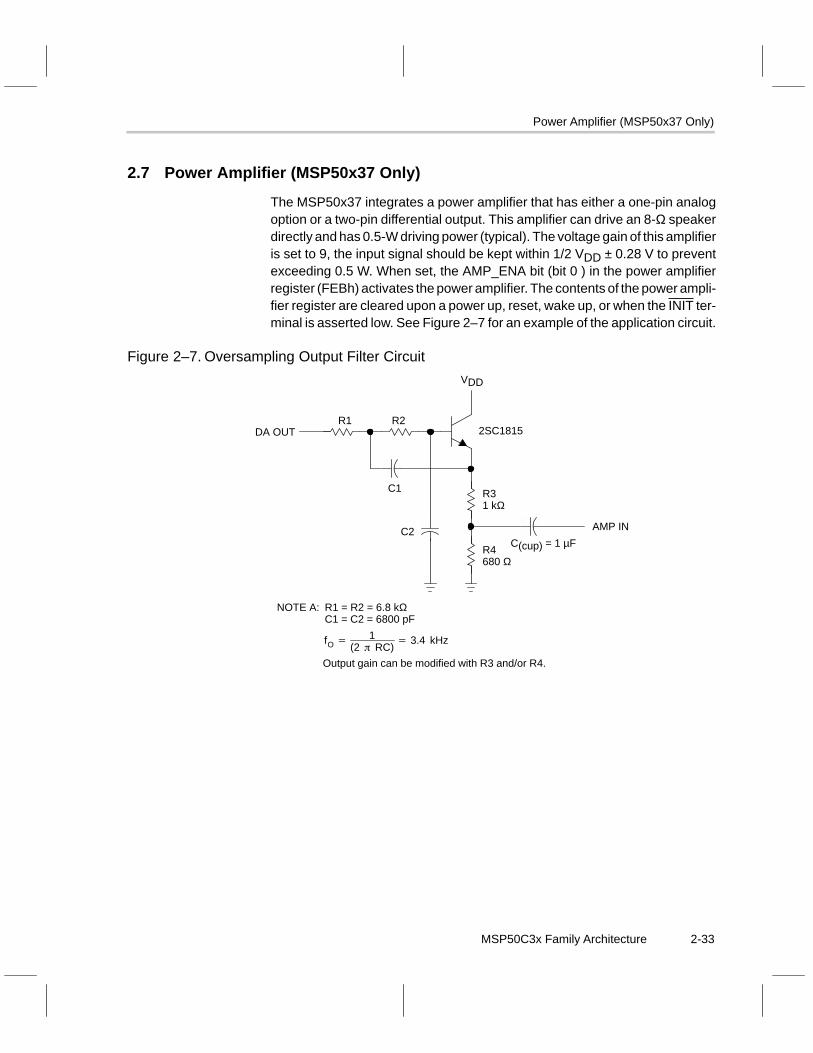
Power Amplifier (MSP50x37 Only)
2-33 MSP50C3x Family Architecture
2.7 Power Amplifier (MSP50x37 Only)
The MSP50x37 integrates a power amplifier that has either a one-pin analogoption or a two-pin differential output. This amplifier can drive an 8-Ω speakerdirectly and has 0.5-W driving power (typical). The voltage gain of this amplifieris set to 9, the input signal should be kept within 1/2 VDD ± 0.28 V to preventexceeding 0.5 W. When set, the AMP_ENA bit (bit 0 ) in the power amplifierregister (FEBh) activates the power amplifier. The contents of the power ampli-fier register are cleared upon a power up, reset, wake up, or when the INIT ter-minal is asserted low. See Figure 2–7 for an example of the application circuit.
Figure 2–7. Oversampling Output Filter Circuit
DA OUTR1 R2
VDD
2SC1815
C(cup) = 1 µF
AMP INC2
C1
NOTE A: R1 = R2 = 6.8 kΩC1 = C2 = 6800 pF
fO1
(2 RC) 3.4 kHz
Output gain can be modified with R3 and/or R4.
R31 kΩ
R4680 Ω

2-34
3-1
MSP50C3x Assembler
The MSP50C3x assembler chapter describes how to invoke the assembler,assembler command-line options, source-statement format, assembler sym-bols and characters, and assembler directives.
Topic Page
3.1 Description of Notation Used 3-2. . . . . . . . . . . . . . . . . . . . . . . . . . . . . . . . . .
3.2 Invoking the Assembler 3-3. . . . . . . . . . . . . . . . . . . . . . . . . . . . . . . . . . . . . . .
3.3 Command-Line Options 3-4. . . . . . . . . . . . . . . . . . . . . . . . . . . . . . . . . . . . . . .
3.4 Assembler Input and Output Files 3-7. . . . . . . . . . . . . . . . . . . . . . . . . . . . . .
3.5 Source-Statement Format 3-8. . . . . . . . . . . . . . . . . . . . . . . . . . . . . . . . . . . . .
3.6 Symbols 3-11. . . . . . . . . . . . . . . . . . . . . . . . . . . . . . . . . . . . . . . . . . . . . . . . . . . .
3.7 Character Strings 3-12. . . . . . . . . . . . . . . . . . . . . . . . . . . . . . . . . . . . . . . . . . . .
3.8 Expressions 3-13. . . . . . . . . . . . . . . . . . . . . . . . . . . . . . . . . . . . . . . . . . . . . . . . .
3.9 Assembler Directives 3-14. . . . . . . . . . . . . . . . . . . . . . . . . . . . . . . . . . . . . . . . .
3.10 Listing Formats 3-27. . . . . . . . . . . . . . . . . . . . . . . . . . . . . . . . . . . . . . . . . . . . . .
3.11 Placing Binary Data Above #FFFF 3-28. . . . . . . . . . . . . . . . . . . . . . . . . . . . .
Chapter 3
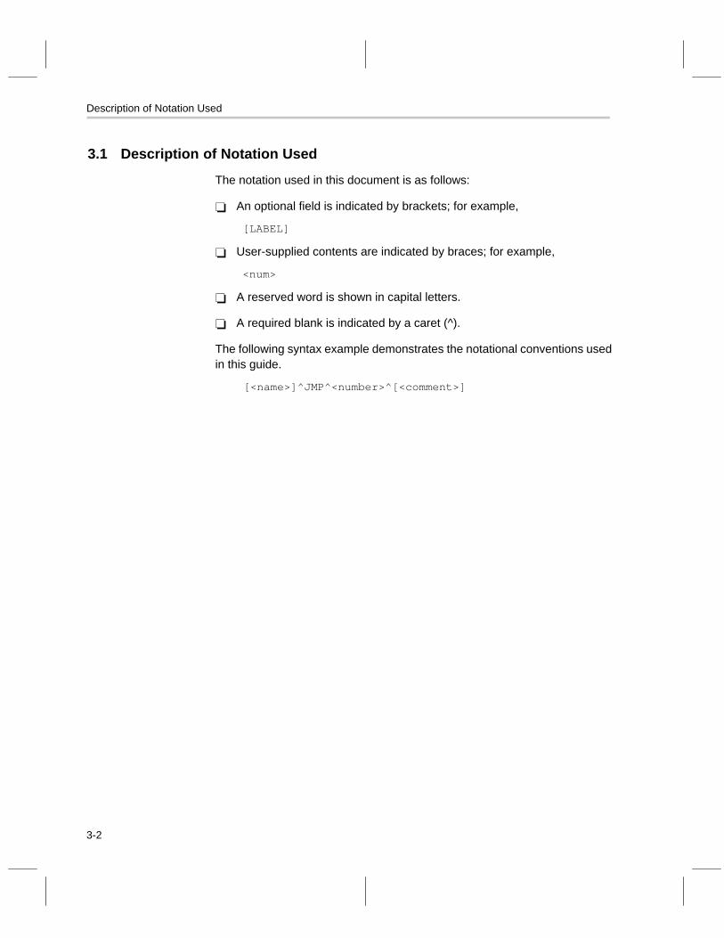
Description of Notation Used
3-2
3.1 Description of Notation Used
The notation used in this document is as follows:
An optional field is indicated by brackets; for example,
[LABEL]
User-supplied contents are indicated by braces; for example,
<num>
A reserved word is shown in capital letters.
A required blank is indicated by a caret (^).
The following syntax example demonstrates the notational conventions usedin this guide.
[<name>]^JMP^<number>^[<comment>]
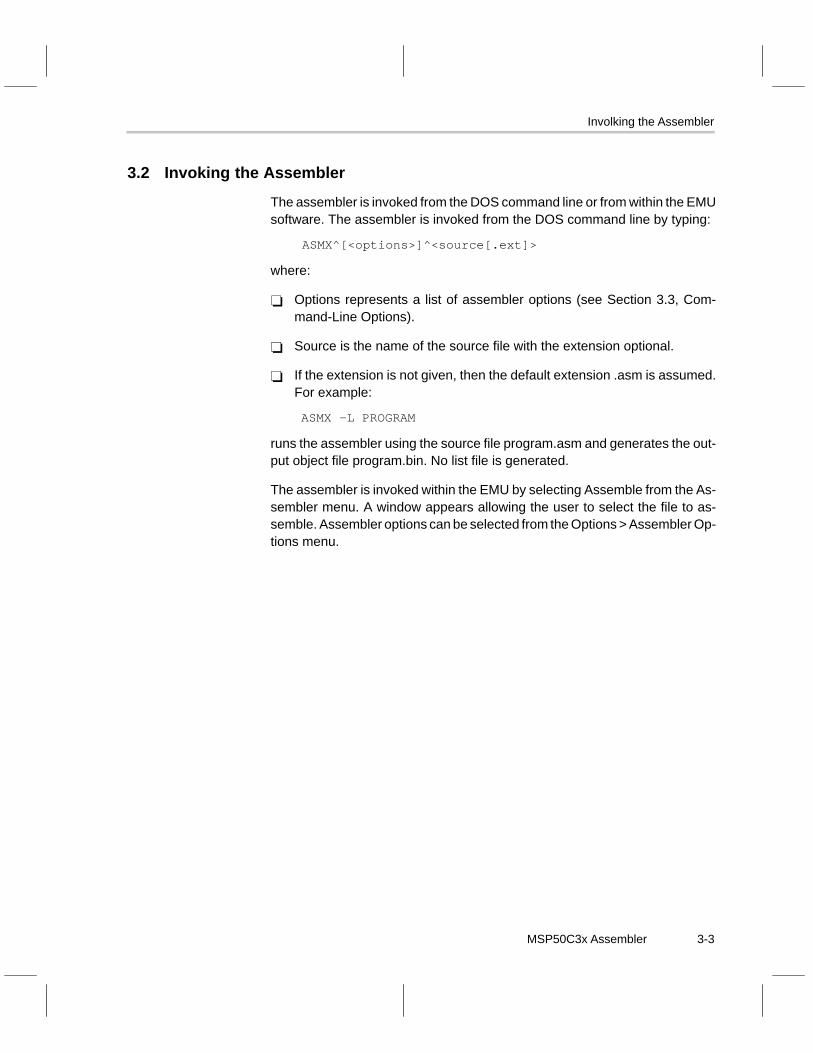
Involking the Assembler
3-3 MSP50C3x Assembler
3.2 Invoking the Assembler
The assembler is invoked from the DOS command line or from within the EMUsoftware. The assembler is invoked from the DOS command line by typing:
ASMX^[<options>]^<source[.ext]>
where:
Options represents a list of assembler options (see Section 3.3, Com-mand-Line Options).
Source is the name of the source file with the extension optional.
If the extension is not given, then the default extension .asm is assumed.For example:
ASMX –L PROGRAM
runs the assembler using the source file program.asm and generates the out-put object file program.bin. No list file is generated.
The assembler is invoked within the EMU by selecting Assemble from the As-sembler menu. A window appears allowing the user to select the file to as-semble. Assembler options can be selected from the Options > Assembler Op-tions menu.
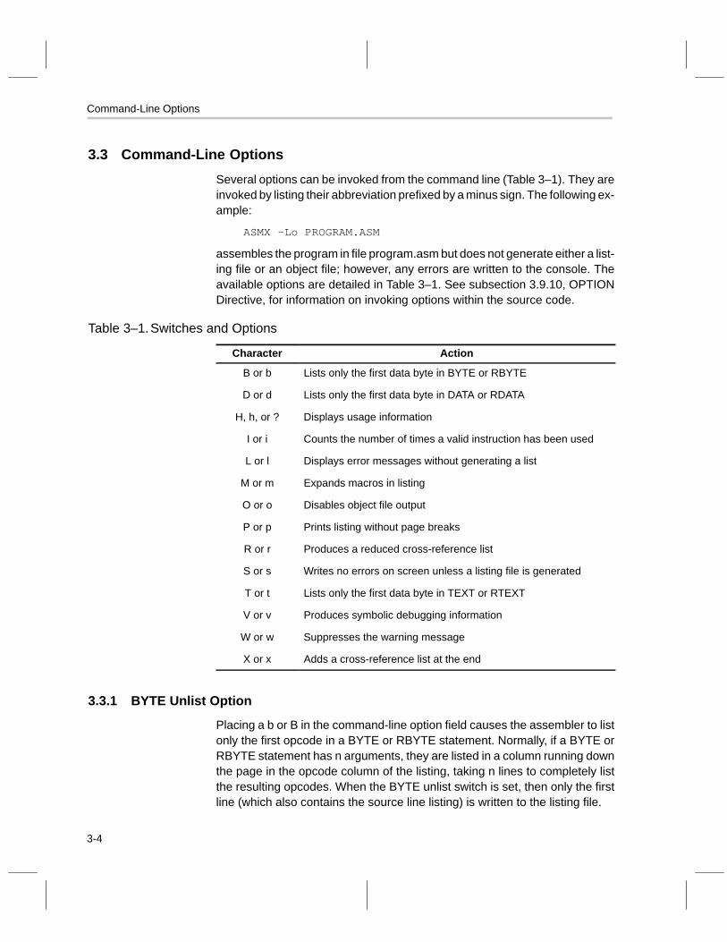
Command-Line Options
3-4
3.3 Command-Line Options
Several options can be invoked from the command line (Table 3–1). They areinvoked by listing their abbreviation prefixed by a minus sign. The following ex-ample:
ASMX –Lo PROGRAM.ASM
assembles the program in file program.asm but does not generate either a list-ing file or an object file; however, any errors are written to the console. Theavailable options are detailed in Table 3–1. See subsection 3.9.10, OPTIONDirective, for information on invoking options within the source code.
Table 3–1.Switches and Options
Character Action
B or b Lists only the first data byte in BYTE or RBYTE
D or d Lists only the first data byte in DATA or RDATA
H, h, or ? Displays usage information
I or i Counts the number of times a valid instruction has been used
L or l Displays error messages without generating a list
M or m Expands macros in listing
O or o Disables object file output
P or p Prints listing without page breaks
R or r Produces a reduced cross-reference list
S or s Writes no errors on screen unless a listing file is generated
T or t Lists only the first data byte in TEXT or RTEXT
V or v Produces symbolic debugging information
W or w Suppresses the warning message
X or x Adds a cross-reference list at the end
3.3.1 BYTE Unlist Option
Placing a b or B in the command-line option field causes the assembler to listonly the first opcode in a BYTE or RBYTE statement. Normally, if a BYTE orRBYTE statement has n arguments, they are listed in a column running downthe page in the opcode column of the listing, taking n lines to completely listthe resulting opcodes. When the BYTE unlist switch is set, then only the firstline (which also contains the source line listing) is written to the listing file.
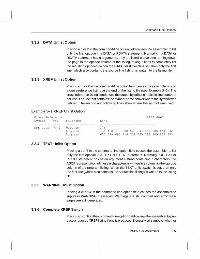
Command-Line Options
3-5 MSP50C3x Assembler
3.3.2 DATA Unlist Option
Placing a d or D in the command-line option field causes the assembler to listonly the first opcode in a DATA or RDATA statement. Normally, if a DATA orRDATA statement has n arguments, they are listed in a column running downthe page in the opcode column of the listing, taking n lines to completely listthe resulting opcodes. When the DATA unlist switch is set, then only the firstline (which also contains the source line listing) is written to the listing file.
3.3.3 XREF Unlist Option
Placing an x or X in the command-line option field causes the assembler to adda cross-reference listing at the end of the listing file (see Example 3–1). Thecross reference listing condenses the output by printing multiple line numbersper line. The line that contains the symbol name shows where the symbol wasdefined. The second and following lines show where the symbol was used.
Example 3–1.XREF Unlist Option
Cross Reference PAGE 0063Symbol Val Filename Line–––––––– –––– ––––––––––––––– ––––––––––––––––––––––––––––––ERR_CODE 0040 big.asm 276 big.asm 434 468 485 508 523 544 567 588 611 632 big.asm 653 674 695 716 738 765 788 809 832 853
3.3.4 TEXT Unlist Option
Placing a t or T in the command-line option field causes the assembler to listonly the first opcode in a TEXT or RTEXT statement. Normally, if a TEXT orRTEXT statement has as an argument a string containing n characters, theASCII representation of these n characters is written in a column in the opcodecolumn of the program listing. When the TEXT unlist switch is set, then onlythe first line (which also contains the source line listing) is written to the listingfile.
3.3.5 WARNING Unlist Option
Placing a w or W in the command-line option field causes the assembler tosuppress WARNING messages. Warnings are still counted and error mes-sages are still generated.
3.3.6 Complete XREF Switch
Placing an r or R in the command-line option field causes the assembler to pro-duce a reduced XREF listing if one is produced. Normally, all symbols (whether
Command-Line Options
3-6
used or not) are listed in the XREF listing. The r option causes the assemblerto omit from the XREF listing all symbols from the copy files that were neverused.
3.3.7 Object Module Switch
Placing an o or O in the command-line option field causes the assembler tonot generate any object output modules.
3.3.8 Listing File Switch
Placing an l or L in the command-line option field causes the assembler to notgenerate the listing file but to display any error messages to the screen.
3.3.9 Page-Eject Disable Switch
Placing a p or P in the command-line option field causes the assembler to printthe listing in a continual manner without division into separate pages. Whendesired, a form feed can still be forced using the PAGE command.
3.3.10 Error-to-Screen Switch
Placing an s or S in the command-line option field causes the assembler to notwrite errors to the screen unless no listing file is being generated.
3.3.11 Instruction Count Switch
Placing an i or I in the command-line option field causes the assembler to gen-erate a table containing the number of times each valid instruction is used inthe program.
3.3.12 Show Usage Switch
Placing an h, H, or ? in the command line option field causes the assemblerto display the proper DOS command line usage and a table of the commandline switches that can be used.
3.3.13 Macro Switch
Placing an m or M in the command-line option field causes the assembler toexpand macros in the listing file.
3.3.14 Symbolic Debugging Switch
Placing a v or V in the command-line option field causes the assembler to pro-duce symbolic debugging information.
Assembler Input and Output Files
3-7 MSP50C3x Assembler
3.4 Assembler Input and Output Files
The assembler takes as input a file containing the assembler source and pro-duces as output a listing file and an object file in binary format.
3.4.1 Assembler Source File
The assembly source file is specified in the command line. When the filenamein the command line has an extension, then the file name is used as given. Ifno extension is specified, then the extension .asm is assumed.
For example:
ASMX PROGRAM.SRC
uses the file program.src as the assembly source file.
ASMX PROGRAM
uses the file program.asm as the assembly source file.
3.4.2 Assembler Binary Object File
The assembly process produces an object file in binary format. The object out-put is placed into a file with the same filename as the assembly source exceptthat the extension is .bin. When the binary file is not desired, it can be disabledeither as a command-line option or with an OPTION statement.
For example:
ASMX PROGRAM.SRC
uses the file program.src as the assembly source file and the file program.binas the binary object output file.
ASMX –o PROGRAM.SRC
uses the file program.src as the assembly source file and produces no objectoutput.
3.4.3 Assembler Listing File
The assembly process produces a listing file that contains the source instruc-tions, the assembled code, and (optionally) a cross-reference table. The listingfile is placed in a file with the same file name as the assembly source exceptthat the extension is .lst.
For example:
ASMX PROGRAM.SRC
uses the file program.src as the assembly source file and the file program.lstas the assembly listing file.
Source Statement Format
3-8
3.5 Source Statement Format
An assembly-language source program consists of source statements con-tained in the assembly source file(s) that can contain assembler directives,machine instructions, or comments. Source statements can contain four or-dered fields separated by one or more blanks. These fields (label, command,operand, and comment) are discussed in the following paragraphs.
The source statement can be as long as 80 characters. When the form widthis set to 80 characters (the default), the assembler truncates the source lineat 60 characters. The user should ensure that nothing other than commentsextend past column 60.
Any source line starting with an asterisk (*) in the first character position or any-thing following a semicolon is treated as a comment in its entirety. It is ignoredby the assembler and has no affect on the assembly process.
The syntax of the source statements is:
[<label>]^COMMAND^<operand>^;[<comment>]
A source statement can have an optional label that is defined by the user. Oneor more blanks separate the label from the COMMAND mnemonic. One ormore blanks separate the mnemonic from the operand (if required by the com-mand). One or more blanks separate the operand from the comment field.Comments are ignored by the assembler.
3.5.1 Label Field
The label field begins in character position one of the source line. When posi-tion one is a character other than a blank or an asterisk, the assembler as-sumes that the symbol is a label. When a label is omitted, then the first charac-ter position must be a blank. The label can contain up to ten characters consist-ing of alphabetic characters (a–z, A–Z), numbers (0–9), and some other char-acters (@,$,_). The first character should be an alphabetic character, and theremaining nine character positions can be any of the legal characters listedabove.
3.5.2 Command Field
The command field begins after the blank that terminates the label field or inthe first nonblank character past the first character position (which must beblank when the label is omitted). The command field is terminated by one ormore blanks and can not extend past the sixtieth character position. The com-mand field can contain either an assembler mnemonic (e.g. TAX) or an assem-
Source Statement Format
3-9 MSP50C3x Assembler
bler directive (e.g. OPTION). The assembler does not distinguish betweencapital and small letters in the command name; for example, TAX, Tax, and tAXare all identical names to the assembler.
3.5.3 Operand Field
The operand field begins following the blank that terminates the commandfield and can not extend past the sixtieth column position. The operand cancontain one or more constants or expressions described in subsection 3.5.5,Constants, through subsection 3.5.5.5, Assembly-Time Constants. Terms inthe operand field are separated by commas. The operand field is terminatedby the first blank encountered.
3.5.4 Comment Field
The comment field begins either after the blank that terminates the operandfield or after the blank that terminates the command field if no operand is re-quired. The comment field must begin with a semicolon. The assembler gener-ates errors if there are comments without the leading semicolon. The commentfield can extend to the end of the source record and can contain any ASCIIcharacter including blanks.
3.5.5 Constants
The assembler recognizes the following five types of constants:
Decimal integer constants Binary integer constants Hexadecimal integer constants Character constants Assembly-time constants
3.5.5.1 Decimal Integer Constants
A decimal integer constant is written as a string of decimal digits. The rangeof values of decimal integers is –32,768 to 65,535. Positive decimal integerconstants greater than 32,767 are considered negative when interpreted astwo’s complement values.
The following are valid decimal constants:
1000 Constant equal 1000 or 03E8h –32768 Constant equal to –32,768 to 8000h 25 Constant equal to 25 or 0019h
Source Statement Format
3-10
3.5.5.2 Binary Integer Constants
A binary integer constant is written as a string of up to 16 binary digits (0/1)preceded by a question mark (?). When less than 16 digits are specified, theassembler right-justifies the given bits in the resulting constant.
The following are valid binary constants:
?0000000000010011 Constant equal 19 or 0013h ?0111111111111111 Constant equal to 32,767 to 7FFFh ?11110 Constant equal to 30 or 001Eh
3.5.5.3 Hexadecimal Integer Constants
A hexadecimal integer constant is written as a string of up to four hexadecimaldigits preceded by a number sign (#) or a greater than sign (>). When less thanfour hexadecimal digits are specified, the assembler right-justifies the bits thatare specified in the resulting constant. Hexadecimal digits include the decimalvalues 0 through 9 and the letters a (or A) through f (or F).
The following are valid hexadecimal constants:
#07F Constant equal 127 or 07Fh >07f Constant equal 127 or 07Fh #307A Constant equal to 12,410 or 307Ah
3.5.5.4 Character Constants
A character constant is written as a string of one or two alphabetic charactersenclosed in single quotes. A single quote can be represented within the char-acter constant by two successive quotes. When less than two characters arespecified, the assembler right-justifies the given bits in the resulting constant.The characters are represented internally as 8-bit ASCII characters. A charac-ter constant consisting of only two single quotes (no character) is valid and isassigned the value 0000h.
The following are valid character constants:
‘AB’ Constant equal 4142h ‘C’ Constant equal 0043h ‘’’D’ Constant equal to 2744h
3.5.5.5 Assembly-Time Constants
An assembly-time constant is a symbol given a value by an EQU directive (seesubsection 3.9.5, EQU Directive). The value of the symbol is determined at as-sembly time and can be assigned values with expressions using any of theconstant types.
Symbols
3-11 MSP50C3x Assembler
3.6 Symbols
Symbols are used in the label field and the operand field. A symbol is a stringof ten or fewer alphanumeric characters (a–z, A–Z,0–9, and the characters @,_, and $). Upper-case and lower-case characters are not distinguished fromone another; for example, A1 and a1 are treated identically by the assembler.No character can be blank. When more than ten characters are used in a sym-bol, the assembler prints all the characters but issues a warning message thatthe symbol has been truncated and uses only the first ten characters for pro-cessing.
Symbols used in the label field become symbolic addresses. They areassociated with locations in the program and must not be used in the label fieldof other statements. Mnemonic operation codes and assembler directives canalso be used as valid user-defined symbols when placed in the label field.
Symbols used in the operand field must be defined in the assembly, usuallyby appearing in the label field of a statement or in the operand field of an EQUdirective.
The following are examples of valid symbols:
START
Start
Strt_1
Predefined Symbol $
The dollar sign ($) is a predefined symbol given the value of the current loca-tion within the program. It can be used in the operand field to indicate relativeprogram offsets.
For example:
BR $+6
results in a branch to an address six bytes beyond the current location.
Character Strings
3-12
3.7 Character Strings
Several assembler directives require character strings in the operand field. Acharacter string is written as a string of characters enclosed in single quotes.A quote can be represented in the string by two successive quotes. The maxi-mum length of the string is defined for each directive that requires a characterstring. The characters are represented internally in 8-bit ASCII.
The following are valid character strings:
‘SAMPLE PROGRAM’
‘Plan ‘C’’’
Expressions
3-13 MSP50C3x Family Architecture
3.8 Expressions
Expressions are used in the operand fields of assembler instructions and di-rectives. An expression is a constant or symbol, a series of constants or sym-bols, or a series of constants and symbols separated by arithmetic operators.
Each constant or symbol can be preceded by a minus sign (unary minus) ora plus sign (unary plus). Unary minus is the same as taking the two’s comple-ment of the value. An expression must not contain embedded blanks. The validrange of values in an expression is –32,768 to 65,535. The value of all termsof an expression must be known at assembly time.
3.8.1 Arithmetic Operators in Expressions
The following arithmetic operators can be used in an expression:
~ inversion
+ addition
– subtraction
* multiplication
/ division (remainder is truncated)
% modulo (remainder after division)
& bitwise AND
+ + bitwise OR
&& bitwise EXCLUSIVE-OR
In evaluating an expression, the assembler first negates any constant or sym-bol preceded by a unary minus and then performs the arithmetic operationsfrom left to right. The assembler does not assign arithmetic operation prece-dence to any operation other than unary plus and unary minus (so that the ex-pression 4+4*2 is evaluated as 16, not 12).
3.8.2 Parentheses in Expressions
The assembler supports the use of parentheses in expressions to alter the or-der of evaluating the expression. Nesting parentheses within expressions isalso supported. When parentheses are used, the portion of the expressionwithin the innermost parentheses is evaluated first, and then the portion of theexpression within the next innermost pair is evaluated. When evaluation of theportions of the expression within the parentheses has been completed, theevaluation is completed from left to right. Evaluation of portions of an expres-sion within parentheses at the same nesting level is considered as simulta-neous. Parenthetical expressions can not be nested more than eight deep.
Assembler Directives
3-14
3.9 Assembler Directives
Assembler directives (Table 3–2) are instructions that modify the assembleroperation. They are invoked by placing the directive mnemonic in the com-mand field and any modifying operands in the operand field. The valid direc-tives are described in the following paragraphs.
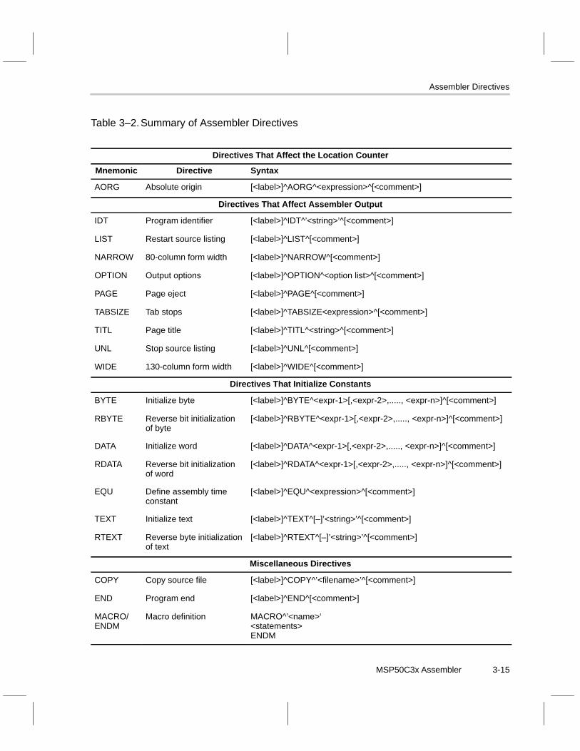
Assembler Directives
3-15 MSP50C3x Assembler
Table 3–2.Summary of Assembler Directives
Directives That Affect the Location Counter
Mnemonic Directive Syntax
AORG Absolute origin [<label>]^AORG^<expression>^[<comment>]
Directives That Affect Assembler Output
IDT Program identifier [<label>]^IDT^’<string>’^[<comment>]
LIST Restart source listing [<label>]^LIST^[<comment>]
NARROW 80-column form width [<label>]^NARROW^[<comment>]
OPTION Output options [<label>]^OPTION^<option list>^[<comment>]
PAGE Page eject [<label>]^PAGE^[<comment>]
TABSIZE Tab stops [<label>]^TABSIZE<expression>^[<comment>]
TITL Page title [<label>]^TITL^<string>^[<comment>]
UNL Stop source listing [<label>]^UNL^[<comment>]
WIDE 130-column form width [<label>]^WIDE^[<comment>]
Directives That Initialize Constants
BYTE Initialize byte [<label>]^BYTE^<expr-1>[,<expr-2>,....., <expr-n>]^[<comment>]
RBYTE Reverse bit initializationof byte
[<label>]^RBYTE^<expr-1>[,<expr-2>,....., <expr-n>]^[<comment>]
DATA Initialize word [<label>]^DATA^<expr-1>[,<expr-2>,....., <expr-n>]^[<comment>]
RDATA Reverse bit initializationof word
[<label>]^RDATA^<expr-1>[,<expr-2>,....., <expr-n>]^[<comment>]
EQU Define assembly timeconstant
[<label>]^EQU^<expression>^[<comment>]
TEXT Initialize text [<label>]^TEXT^[–]’<string>’^[<comment>]
RTEXT Reverse byte initializationof text
[<label>]^RTEXT^[–]’<string>’^[<comment>]
Miscellaneous Directives
COPY Copy source file [<label>]^COPY^’<filename>’^[<comment>]
END Program end [<label>]^END^[<comment>]
MACRO/ENDM
Macro definition MACRO^’<name>‘<statements>ENDM
Assembler Directives
3-16
3.9.1 AORG Directive
The AORG directive places the value found in the expression in the operandfield into the location counter. Subsequent instructions have addresses start-ing at this value. The use of the label field is optional, but when a label is used,it is assigned the value found in the operand field.
The syntax of the AORG directive is as follows:
[<label>]^AORG^<expression>^[<comment>]
In the following statement:
AORG #1000+offset
if the offset has a value of 8, AORG sets the location counter to #1008. If a labelis included, it also is assigned the value of #1008. The symbol offset must bepreviously defined.
3.9.2 BYTE Directive
The BYTE directive places the value of one or more expressions into succes-sive bytes of program memory. The range of each term is 0 to 255. The com-mand field contains BYTE. The operand field contains a series of one or moreterms separated by commas and terminated by a blank that represents the val-ues to be placed in the successive bytes of program memory.
The syntax of the BYTE directive is as follows:
[<label>]^BYTE^<expr_1>[,<expr_2>,...,<expr_n>]^[<comment>]
In the following statement:
BYTE #E0,5,data+5
places the numbers 224, 5, and the result of the arithmetic operation data +5 into the next three bytes of program memory. The value of the symbol datamust be defined in the assembly process.
3.9.3 COPY Directive
The COPY directive causes the assembler to read source statements from adifferent file. The assembler gets subsequent statements from the copy file un-til either the end-of-file marker is found or an END directive is found in the copyfile. A copy file cannot contain another COPY directive. The command fieldcontains COPY. The operand field contains the name of the file from which thesource files are to be read.
Assembler Directives
3-17 MSP50C3x Assembler
The syntax of the COPY directive is as follows:
[<label>]^COPY^’<filename>‘^[<comment>]
The directive in the following example:
COPY ‘copy.fil’
causes the assembler to take its source statements from a file called copy.fil.At the end-of-file for copy.fil or when an END directive is encountered incopy.fil, the assembler resumes processing source statements from the origi-nal source file. The single quotes around the filename are required by the as-sembler.
3.9.4 DATA Directive
The DATA directive places the value of one or more expressions into succes-sive words of program memory. The range of each term is 0 to 65,535. Thecommand field contains DATA. The operand field contains a series of one ormore terms separated by commas and terminated by a blank that representsthe values to be placed in the successive words of program memory.
The syntax of the DATA directive is as follows:
[<label>]^DATA^<expr_1>[,<expr_2>,...,<expr_n>]^[<comment>]
In the following statement:
DATA #E000,’AB’
places the following bytes into successive locations in program memory: E0h,00h, 41h, 42h
3.9.5 EQU Directive
The EQU directive assigns a value to a symbol. The label field contains thename of the symbol to which a value is assigned. The command field containsEQU. The operand field contains the value to be assigned to the symbol.
The syntax of the EQU directive is as follows:
[<label>]^EQU^<expression>^[<comment>]
In the following statement:
Offset EQU #100
assigns the numeric value of 256 (100h) to the symbol Offset.
3.9.6 END Directive
The END directive signals the end of the source or copy file. It is treated by theprogram as an end-of-file marker. When it is found in a copy file, the copy file
Assembler Directives
3-18
is closed and subsequent statements are taken from the source file. When itis found in the source file, the assembly process terminates at that point in thefile.
The syntax of the END directive is as follows:
[<label>]^END^<comment>]
In the following statement:
ACAAC 1 END CLA
the ACAAC 1 instruction is assembled, but the CLA and any subsequentinstructions are ignored.
3.9.7 IDT Directive
The IDT assigns a name to the object module produced. Use of the label fieldis optional. When used, a label assumes the current value of the locationcounter. The command field contains IDT. The operand field contains the mod-ule name <string>, a character string of up to eight characters within singlequotes. When a character string of more than eight characters is entered, theassembler prints a truncation warning message and retains the first eight char-acters as the program name.
The syntax of the IDT directive is as follows:
[<label>]^IDT^<string>^[<comment>]
In the following example:
AORG 20L1 IDT ‘Example’
assigns the value of 20 to the symbol L1 and assigns the name ‘Example’ tothe module being assembled. The module name is then printed in the sourcelisting as the operand of the IDT directive and appears in the page heading ofthe source listing.
3.9.8 LIST Directive
The LIST directive restores printing of the source listing. This directive is re-quired only when a no-source-listing (UNL) directive is in effect and causes theassembler to resume listing. This directive is not printed in the source listing,but the line counter increments.
The syntax of the LIST directive is as follows:
Assembler Directives
3-19 MSP50C3x Assembler
[<label>]^LIST^[<comment>]
In the following statement:
AORG 10T1 LIST ;Turn on source listing
the label T1 is assigned the value 10 and listing is resumed. The line is notprinted out so that although the label T1 is entered into the symbol table andappears in the cross-reference listing, the line in which it is assigned a valuedoes not appear in the listing file.
3.9.9 NARROW Directive
The NARROW directive causes the assembler to assume an 80-column formwidth for the listing file. The default is 80 columns (See subsection 3.9.18,Wide Directive).
The syntax of the NARROW directive is as follows:
[<label>]^NARROW^[<comment>]
The following example uses the NARROW directive:
AORG 10T1 NARROW ;Switch to 80–column listing format.
3.9.10 OPTION Directive
The OPTION directive selects several options that affect assembler operation.The <option list> operand is a list of keywords separated by commas; eachkeyword selects an assembly feature. Only the first character of the keywordis significant. Use of the label field is optional. When used, the label assumesthe current value of the location counter.
The syntax of the OPTION directive is as follows:
[<label>]^OPTION^<option–list>^[<comment>]
The following are examples of the OPTION directive:
OPTION XREF,SCRNOFOPTION X,S
The two examples above have identical effects. The cross-reference listing isproduced and the error messages are not sent to the screen (unless no sourcelisting file is being produced). See Section 3.3, Command-Line Options, for in-formation on invoking options from the command line.
The available options are listed in the following paragraphs.
Assembler Directives
3-20
3.9.10.1 BUNLST – Byte Unlist Option
Placing any valid symbol starting with B or b in the option list enables the byteunlist option. This option limits the listing of BYTE or RBYTE directives to oneline. Normally, if a BYTE or RBYTE directive has more than one operand, theresulting object code is listed in a column in the opcode column of the sourcelisting. BUNLST is used to avoid this.
3.9.10.2 DUNLST – Data Unlist Option
Placing any valid symbol starting with D or d in the option list enables the dataunlist option. This option limits the listing of DATA or RDATA directives to oneline. Normally, if a DATA or RDATA directive has more than one operand, theresulting object code is listed in a column in the opcode column of the sourcelisting. DUNLST is used to avoid this.
3.9.10.3 FUNLST – Byte, Data and Text Unlist Option
Placing any valid symbol starting with F or f in the option limits the listing ofBYTE, RBYTE, DATA, RDATA, TEXT, or RTEXT directives to one line. In ef-fect, it is equivalent to calling the DUNLST, BUNLST, and TUNLST directivesall at the same time.
3.9.10.4 LSTUNL – Listing Unlist Option
Placing any valid symbol starting with L or l in the option list inhibits the listingfile from being produced. It takes precedence over the LIST directive.
3.9.10.5 OBJUNL – Object File Unlist Option
Placing any valid symbol starting with O or o in the option enables the objectfile unlist option. This option inhibits the generation of an object file.
3.9.10.6 PAGEOF – Page Break Inhibit Option
Placing any valid symbol starting with P or p in the option enables the pagebreak inhibit option. This option causes the listing file to be printed in a continu-ous stream without page breaks.
3.9.10.7 RXREF – Reduced XREF Option
Placing any valid symbol starting with R or r in the option enables the reducedXREF option. This option causes symbols that were found in copy files but nev-er used to be omitted from the cross-reference listing (if produced).
3.9.10.8 SCRNOF – Screen Error Message Unlist Option
Placing any valid symbol starting with S or s in the option enables the screenerror message unlist option. This option causes the error messages to not belisted on the screen unless the listing file is not being produced.
Assembler Directives
3-21 MSP50C3x Assembler
3.9.10.9 TUNLST – Text Unlist Option
Placing any valid symbol starting with T or t in the option list enables the textunlist option. This option limits the listing of TEXT or RTEXT directives to oneline. A TEXT or RTEXT directive normally takes as many lines to list as thereare characters in the operand. TUNLST causes only the first line of the direc-tive listing to be produced.
3.9.10.10 WARNOFF – Warning Message Unlist Option
Placing any valid symbol starting with W or w in the option list inhibits the listingof warning diagnostics. Warnings are still counted and the total is still printedat the end of the source listing.
3.9.10.11 XREF – Cross-Reference Listing Enable
Placing any valid symbol starting with X or x in the option list causes a cross-reference listing to be produced at the end of the source listing. When used,it should be placed at the start of the program.
3.9.11 PAGE Directive
The PAGE directive forces the assembler to continue the source program list-ing on a new page. The PAGE directive is not printed in the source listing, butthe line counter increments. Use of the label field is optional. When used, alabel assumes the current value of the location counter. The command fieldcontains PAGE. The operand field is not used.
The syntax of the PAGE directive is as follows:
[<label>]^PAGE^[<comment>]
In the following statement:
AORG 10
T1 PAGE ;Force page eject
the label T1 is assigned the value 10 and the listing is resumed at the top ofthe next page. The line is not printed out so that although the label T1 is enteredinto the symbol table and appears in the cross-reference listing, the line inwhich it is assigned a value does not appear in the listing file.
3.9.12 RBYTE Directive
The RBYTE directive places the value of one or more expressions into succes-sive bytes of program memory in a bit-reversed form. The range of each term
Assembler Directives
3-22
is 0 to 255. The command field contains RBYTE. The operand field containsa series of one or more terms separated by commas and terminated by a blankthat represents the values to be placed in the successive bytes of programmemory.
The syntax of the RBYTE directive is as follows:
[<label>]^RBYTE^<expr_1>[,<expr_2>,...,<expr_n>]^[<comment>]
In the following statement:
RBYTE #E0,5,data+5
places the numbers 7 (07h), 160 (A0h), and the bit reversed result of the arith-metic operation data+5 into the next three bytes of program memory. The val-ue of the symbol data must be defined in the assembly process.
3.9.13 RDATA Directive
The RDATA directive places the value of one or more expressions into succes-sive words of program memory in a bit-reversed form. The range of each termis 0 to 65,535. The command field contains RDATA. The operand field containsa series of one or more terms separated by commas and terminated by a blankthat represents the values to be placed in the successive words of programmemory.
The syntax of the RDATA directive is as follows:
[<label>]^RDATA^<expr_1>[,<expr_2>,...,<expr_n>]^[<comment>]
In the following statement:
RDATA #E000,’AB’
places the following bytes into successive locations in program memory: 00h,07h, 42h, 82h
3.9.14 RTEXT Directive
The RTEXT directive writes an ASCII string to the object file in reverse order.When the string is preceded by a minus sign, the last character in the stringto be written (which is the first character of the string as given) is written withits most significant bit set to 1. The use of the label field is optional. When used,the label assumes the current value of the location counter. The command fieldcontains RTEXT. The operand field contains a character string of up to 52 char-acters long enclosed in single quotes (optionally preceded by a minus sign).
Assembler Directives
3-23 MSP50C3x Assembler
The syntax of the RTEXT directive is as follows:
[<label>]^RTEXT^[–]’<string>‘^[<comment>]
In the following examples:
RTEXT –’This is a test’ RTEXT ‘This is a test’
both write the string “tset a si sihT” to the output file. The first example writesthe first T in the word “This”, which is the last character to be written with itsmost significant bit set to 1 (that is, as a D4h instead of a 54h).
3.9.15 TEXT Directive
The TEXT directive writes an ASCII string to the object file. When the stringis preceded by a minus sign, the last character in the string is written with itsmost significant bit set to 1. The use of the label field is optional. When used,the label assumes the current value of the location counter. The command fieldcontains TEXT. The operand field contains a character string of up to 52 char-acters long enclosed in single quotes (optionally preceded by a minus sign).
The syntax of the TEXT directive is as follows:
[<label>]^TEXT^[–]’<string>‘^[<comment>]
In the following examples:
RTEXT –’This is a test’ RTEXT ‘This is a test’
both write the string This is a test to the output file. The first example writes thefinal ‘t’ in the word “test” with its most significant bit set to 1 (that is, as a F4hinstead of a 74h).
3.9.16 TITL Directive
The TITL directive inserts a title to be printed in the heading of each page ofthe source listing. When a title is desired in the heading of the listing page, aTITL directive must be the first source statement submitted to the assembler.Unlike the IDT directive, the TITL directive is not printed in the source listing.The assembler does not print the comment because the TITL directive is notprinted, but the line counter does increment. Use of the label field is optional.When used, a label field assumes the current value of the location counter. Thecommand field contains TITL. The operand field contains the title (string)–acharacter string of up to 50 characters in length enclosed in single quotes.When more than 50 characters are entered, the assembler retains the first
Assembler Directives
3-24
50 characters as the title and prints a syntax error message. The comment fieldis optional.
The syntax of the TITL directive is as follows:
[<label>]^TITL^[–]’<string>‘^[<comment>]
In the following example:
TITL ’Sample Program’ This is a sample line
causes the title, Sample Program, to be printed in the page heading of thesource listing. When a TITL directive is the first source statement in a program,the title is printed on all pages until another TITL directive is processed. Other-wise, the title is printed on the page after the directive is processed and on sub-sequent pages until another TITL directive is processed. None of this line isprinted to the listing file.
3.9.17 UNL Directive
The UNL directive inhibits printing of the source listing output until the occur-rence of a LIST directive. It is not printed in the source listing, but the sourceline counter is incremented. The label field assumes the value of the locationcounter. The command field contains the symbol UNL. The operand field is notused.
The syntax of the UNL directive is as follows:
[<label>]^UNL^[<comment>]
In the following statement:
AORG 10T1 UNL Turn off source listing
the label T1 is assigned the value 10 and listing is inhibited.
3.9.18 WIDE Directive
The WIDE directive causes the assembler to assume an 130-column formwidth for the listing file. The default is 80 columns (See subsection 3.9.9, NAR-ROW Directive).
The syntax of the WIDE directive is as follows:
[<label>]^WIDE^[<comment>]
The following example uses the WIDE directive:
Assembler Directives
3-25 MSP50C3x Assembler
AORG 10T1 WIDE Switch to 130–column listing format.
3.9.19 MACRO/ENDM Directive
The MACRO directive allows macros to be defined. Macro expansion allowsfor 10 parameters to be passed to the macro. To reference a parameter, usea leading dollar sign $ followed by a single decimal digit. To include a dollar signin the expansion, use two dollar signs. Nested macro definitions are not sup-ported.
The syntax of the MACRO directive is as follows:
MACRO ‘name’ <statements> ENDM
The following macro FWD jumps forward from the current location counter.
MACRO ‘FWD’ SBR ($$+$0) ENDM
To execute the macro and cause a jump forward by 10 bytes, type
FWD 10
All arguments passed to a macro are resolved before expansion. To preventa symbol from being expanded, enclose the symbol in single quotes. The sym-bol in quotesmust be at least 3 characters in length or incorrect results maybe obtained. Symbols less than 3 characters in length can be padded withspaces to obtain the required 3 character minimum length.
Another example:
TEN EQU 10 MACRO ‘JMP’L$0 SBR L$1
ENDM
Using the following calls,
JMP TEN,’TEN’ JMP ‘TEN’,TEN
expands to:
L10 SBR LTENLTEN SBR L10
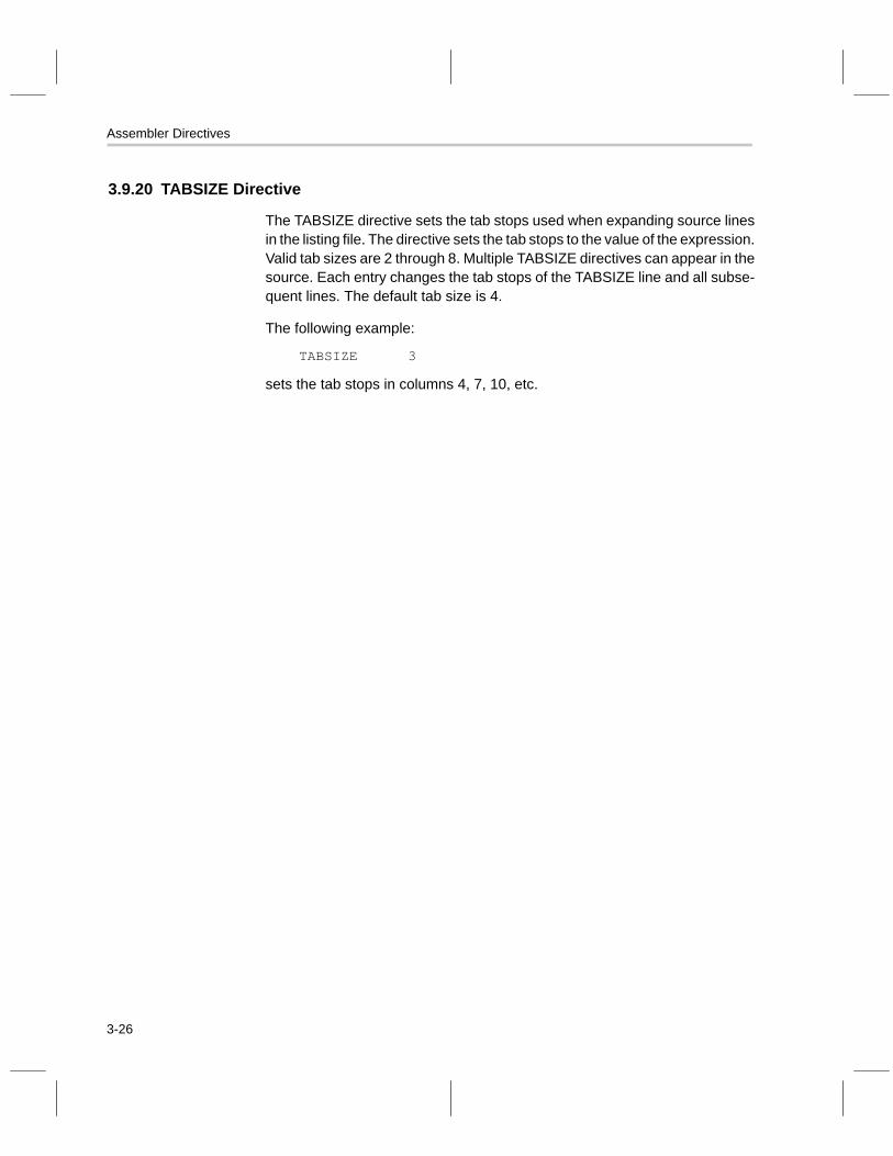
Assembler Directives
3-26
3.9.20 TABSIZE Directive
The TABSIZE directive sets the tab stops used when expanding source linesin the listing file. The directive sets the tab stops to the value of the expression.Valid tab sizes are 2 through 8. Multiple TABSIZE directives can appear in thesource. Each entry changes the tab stops of the TABSIZE line and all subse-quent lines. The default tab size is 4.
The following example:
TABSIZE 3
sets the tab stops in columns 4, 7, 10, etc.
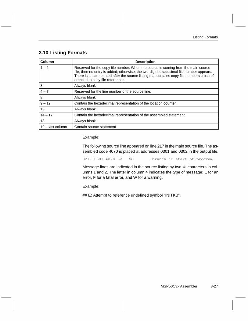
Listing Formats
3-27 MSP50C3x Assembler
3.10 Listing Formats
Column Description
1 – 2 Reserved for the copy file number. When the source is coming from the main sourcefile, then no entry is added; otherwise, the two-digit hexadecimal file number appears.There is a table printed after the source listing that contains copy file numbers crossref-erenced to copy file references.
3 Always blank
4 – 7 Reserved for the line number of the source line.
8 Always blank
9 – 12 Contain the hexadecimal representation of the location counter.
13 Always blank
14 – 17 Contain the hexadecimal representation of the assembled statement.
18 Always blank
19 – last column Contain source statement
Example:
The following source line appeared on line 217 in the main source file. The as-sembled code 4070 is placed at addresses 0301 and 0302 in the output file.
0217 0301 4070 BR GO ;branch to start of program
Message lines are indicated in the source listing by two ‘#’ characters in col-umns 1 and 2. The letter in column 4 indicates the type of message: E for anerror, F for a fatal error, and W for a warning.
Example:
## E: Attempt to reference undefined symbol “INITKB”.
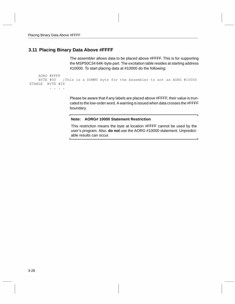
Placing Binary Data Above #FFFF
3-28
3.11 Placing Binary Data Above #FFFF
The assembler allows data to be placed above #FFFF. This is for supportingthe MSP50C34 64K-byte part. The excitation table resides at starting address#10000. To start placing data at #10000 do the following:
AORG #FFFF BYTE #00 ;This is a DUMMY byte for the Assembler to act as AORG #10000ETABLE BYTE #24 . . . .
Please be aware that if any labels are placed above #FFFF, their value is trun-cated to the low-order word. A warning is issued when data crosses the #FFFFboundary.
Note: AORG# 10000 Statement Restriction
This restriction means the byte at location #FFFF cannot be used by theuser’s program. Also, do not use the AORG #10000 statement. Unpredict-able results can occur.
4-1
MSP50x3x Instruction Set
This chapter describes the 61 different MSP50C3x instructions (Table 4–1 andTable 4–2). Each instruction takes either one or two instruction cycles toexecute. Each instruction cycle consists of 16 clock cycles; therefore, a clockspeed of 19.2 MHz translates to 1,200,000 instructions per second. When onesynthesis channel is enabled for LPC, approximately one out of every fourinstruction cycles is taken for synthesis calculations. This causes the instruc-tion cycle rate for the program to drop to approximately 900,000 cycles per se-cond. When both synthesis channels are enabled for LPC, approximately twoout of every four instruction cycles are taken for synthesis calculations. Theprogram instruction-cycle rate for this case is approximately 600,000 cyclesper second.
Topic Page
4.1 Instruction Syntax 4-2. . . . . . . . . . . . . . . . . . . . . . . . . . . . . . . . . . . . . . . . . . . .
4.2 MSP50x3x Assembly Instructions 4-3. . . . . . . . . . . . . . . . . . . . . . . . . . . . . .
Chapter 4
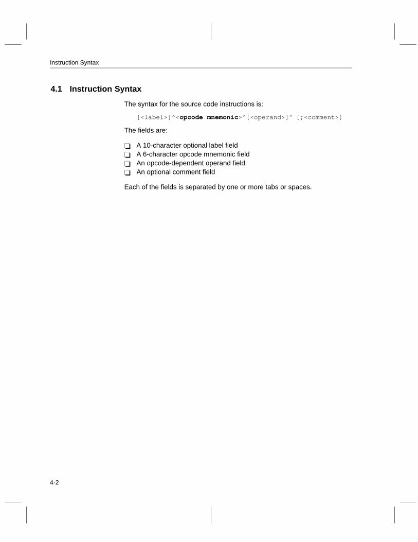
Instruction Syntax
4-2
4.1 Instruction Syntax
The syntax for the source code instructions is:
[<label>]^<opcode mnemonic>^[<operand>]^ [;<comment>]
The fields are:
A 10-character optional label field A 6-character opcode mnemonic field An opcode-dependent operand field An optional comment field
Each of the fields is separated by one or more tabs or spaces.
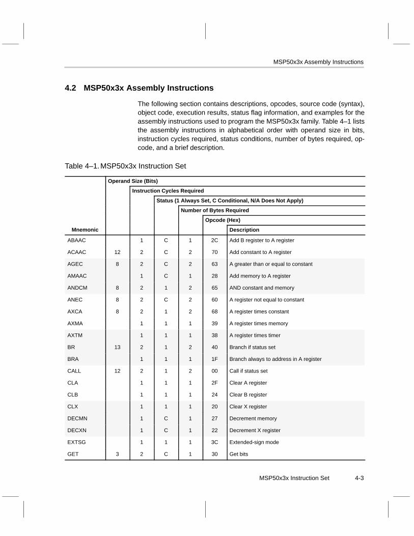
MSP50x3x Assembly Instructions
4-3 MSP50x3x Instruction Set
4.2 MSP50x3x Assembly Instructions
The following section contains descriptions, opcodes, source code (syntax),object code, execution results, status flag information, and examples for theassembly instructions used to program the MSP50x3x family. Table 4–1 liststhe assembly instructions in alphabetical order with operand size in bits,instruction cycles required, status conditions, number of bytes required, op-code, and a brief description.
Table 4–1.MSP50x3x Instruction Set
Operand Size (Bits)
Instruction Cycles Required
Status (1 Always Set, C Conditional, N/A Does Not Apply)
Number of Bytes Required
Opcode (Hex)
Mnemonic Description
ABAAC 1 C 1 2C Add B register to A register
ACAAC 12 2 C 2 70 Add constant to A register
AGEC 8 2 C 2 63 A greater than or equal to constant
AMAAC 1 C 1 28 Add memory to A register
ANDCM 8 2 1 2 65 AND constant and memory
ANEC 8 2 C 2 60 A register not equal to constant
AXCA 8 2 1 2 68 A register times constant
AXMA 1 1 1 39 A register times memory
AXTM 1 1 1 38 A register times timer
BR 13 2 1 2 40 Branch if status set
BRA 1 1 1 1F Branch always to address in A register
CALL 12 2 1 2 00 Call if status set
CLA 1 1 1 2F Clear A register
CLB 1 1 1 24 Clear B register
CLX 1 1 1 20 Clear X register
DECMN 1 C 1 27 Decrement memory
DECXN 1 C 1 22 Decrement X register
EXTSG 1 1 1 3C Extended-sign mode
GET 3 2 C 1 30 Get bits
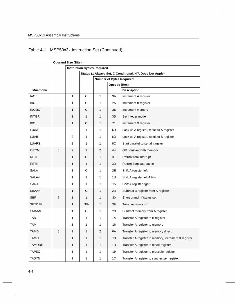
MSP50x3x Assembly Instructions
4-4
Table 4–1. MSP50x3x Instruction Set (Continued)
Operand Size (Bits)
Instruction Cycles Required
Status (1 Always Set, C Conditional, N/A Does Not Apply)
Number of Bytes Required
Opcode (Hex)
Mnemonic Description
IAC 1 C 1 3A Increment A register
IBC 1 C 1 25 Increment B register
INCMC 1 C 1 26 Increment memory
INTGR 1 1 1 3B Set integer mode
IXC 1 C 1 21 Increment X register
LUAA 2 1 1 6B Look up A register, result to A register
LUAB 2 1 1 6D Look up A register, result to B register
LUAPS 2 1 1 6C Start parallel-to-serial transfer
ORCM 8 2 1 2 64 OR constant with memory
RETI 1 C 1 3E Return from interrupt
RETN 1 1 1 3D Return from subroutine
SALA 1 C 1 2E Shift A register left
SALA4 1 1 1 1B Shift A register left 4 bits
SARA 1 1 1 15 Shift A register right
SBAAN 1 C 1 2D Subtract B register from A register
SBR 7 1 1 1 80 Short branch if status set
SETOFF 1 N/A 1 3F Turn processor off
SMAAN 1 C 1 29 Subtract memory from A register
TAB 1 1 1 1A Transfer A register to B register
TAM 1 1 1 16 Transfer A register to memory
TAMD 8 2 1 2 6A Transfer A register to memory direct
TAMIX 1 1 1 13 Transfer A register to memory, increment X register
TAMODE 1 1 1 1D Transfer A register to mode register
TAPSC 1 1 1 19 Transfer A register to prescale register
TASYN 1 1 1 1C Transfer A register to synthesizer register
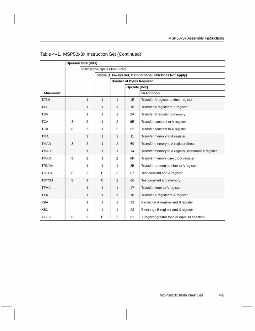
MSP50x3x Assembly Instructions
4-5 MSP50x3x Instruction Set
Table 4–1. MSP50x3x Instruction Set (Continued)
Operand Size (Bits)
Instruction Cycles Required
Status (1 Always Set, C Conditional, N/A Does Not Apply)
Number of Bytes Required
Opcode (Hex)
Mnemonic Description
TATM 1 1 1 1E Transfer A register to timer register
TAX 1 1 1 18 Transfer A register to X register
TBM 1 1 1 2A Transfer B register to memory
TCA 8 2 1 2 6E Transfer constant to A register
TCX 8 2 1 2 62 Transfer constant to X register
TMA 1 1 1 11 Transfer memory to A register
TMAD 8 2 1 2 69 Transfer memory to A register direct
TMAIX 1 1 1 14 Transfer memory to A register, increment X register
TMXD 8 2 1 2 6F Transfer memory direct to X register
TRNDA 1 1 1 2B Transfer random number to A register
TSTCA 8 2 C 2 67 Test constant and A register
TSTCM 8 2 C 2 66 Test constant and memory
TTMA 1 1 1 17 Transfer timer to A register
TXA 1 1 1 10 Transfer X register to A register
XBA 1 1 1 12 Exchange A register and B register
XBX 1 1 1 23 Exchange B register and X register
XGEC 8 2 C 2 61 X register greater than or equal to constant
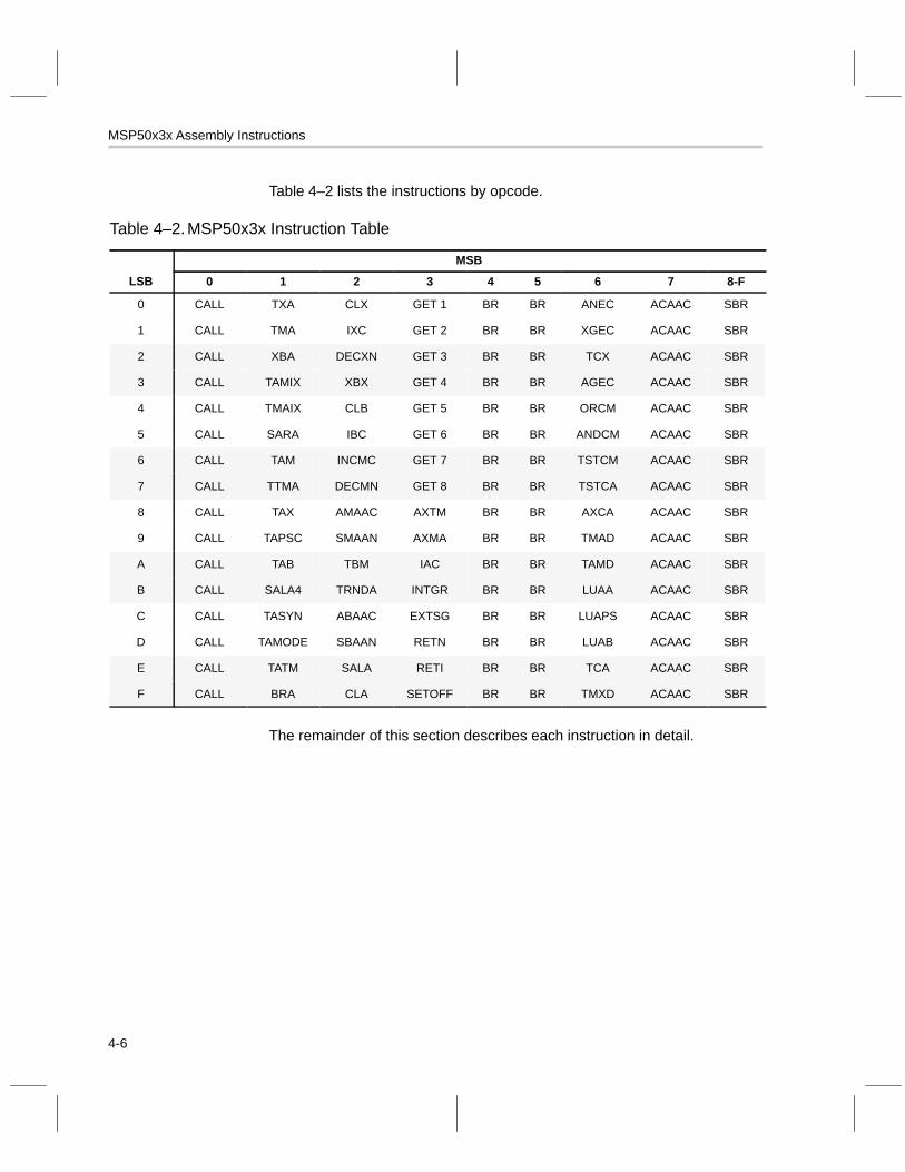
MSP50x3x Assembly Instructions
4-6
Table 4–2 lists the instructions by opcode.
Table 4–2.MSP50x3x Instruction Table
MSB
LSB 0 1 2 3 4 5 6 7 8-F
0 CALL TXA CLX GET 1 BR BR ANEC ACAAC SBR
1 CALL TMA IXC GET 2 BR BR XGEC ACAAC SBR
2 CALL XBA DECXN GET 3 BR BR TCX ACAAC SBR
3 CALL TAMIX XBX GET 4 BR BR AGEC ACAAC SBR
4 CALL TMAIX CLB GET 5 BR BR ORCM ACAAC SBR
5 CALL SARA IBC GET 6 BR BR ANDCM ACAAC SBR
6 CALL TAM INCMC GET 7 BR BR TSTCM ACAAC SBR
7 CALL TTMA DECMN GET 8 BR BR TSTCA ACAAC SBR
8 CALL TAX AMAAC AXTM BR BR AXCA ACAAC SBR
9 CALL TAPSC SMAAN AXMA BR BR TMAD ACAAC SBR
A CALL TAB TBM IAC BR BR TAMD ACAAC SBR
B CALL SALA4 TRNDA INTGR BR BR LUAA ACAAC SBR
C CALL TASYN ABAAC EXTSG BR BR LUAPS ACAAC SBR
D CALL TAMODE SBAAN RETN BR BR LUAB ACAAC SBR
E CALL TATM SALA RETI BR BR TCA ACAAC SBR
F CALL BRA CLA SETOFF BR BR TMXD ACAAC SBR
The remainder of this section describes each instruction in detail.
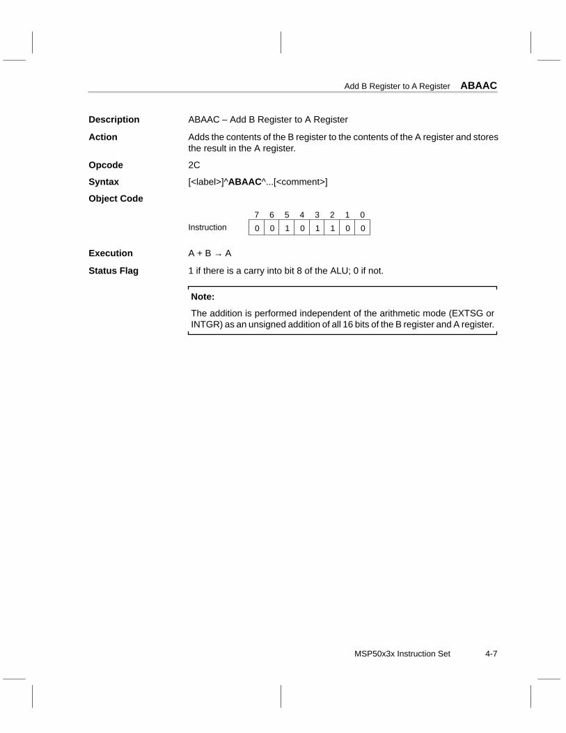
Add B Register to A Register ABAAC
4-7 MSP50x3x Instruction Set
Description ABAAC – Add B Register to A Register
Action Adds the contents of the B register to the contents of the A register and storesthe result in the A register.
Opcode 2C
Syntax [<label>]^ABAAC^...[<comment>]
Object Code
34567 2 1 0
10100 1 0 0Instruction
Execution A + B → A
Status Flag 1 if there is a carry into bit 8 of the ALU; 0 if not.
Note:
The addition is performed independent of the arithmetic mode (EXTSG orINTGR) as an unsigned addition of all 16 bits of the B register and A register.
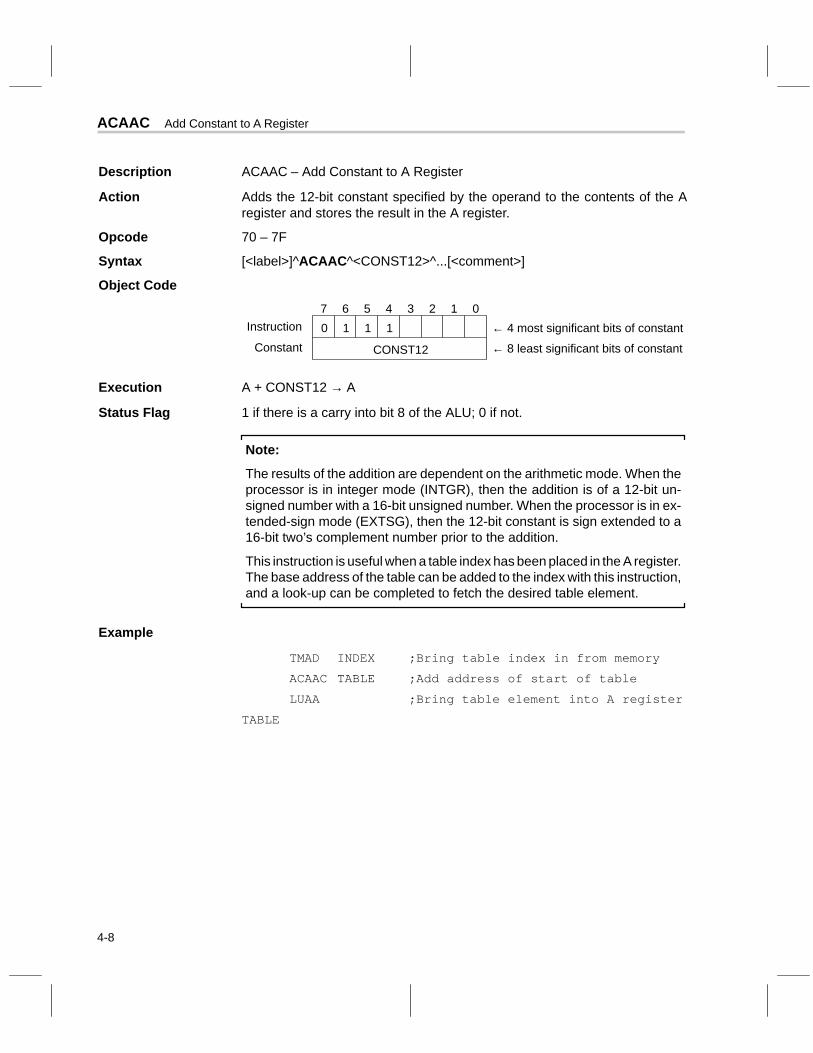
ACAAC Add Constant to A Register
4-8
Description ACAAC – Add Constant to A Register
Action Adds the 12-bit constant specified by the operand to the contents of the Aregister and stores the result in the A register.
Opcode 70 – 7F
Syntax [<label>]^ACAAC^<CONST12>^...[<comment>]
Object Code
34567 2 1 0
1110Instruction
CONST12Constant
← 4 most significant bits of constant
← 8 least significant bits of constant
Execution A + CONST12 → A
Status Flag 1 if there is a carry into bit 8 of the ALU; 0 if not.
Note:
The results of the addition are dependent on the arithmetic mode. When theprocessor is in integer mode (INTGR), then the addition is of a 12-bit un-signed number with a 16-bit unsigned number. When the processor is in ex-tended-sign mode (EXTSG), then the 12-bit constant is sign extended to a16-bit two’s complement number prior to the addition.
This instruction is useful when a table index has been placed in the A register.The base address of the table can be added to the index with this instruction,and a look-up can be completed to fetch the desired table element.
Example
TMAD INDEX ;Bring table index in from memory
ACAAC TABLE ;Add address of start of table
LUAA ;Bring table element into A register
TABLE
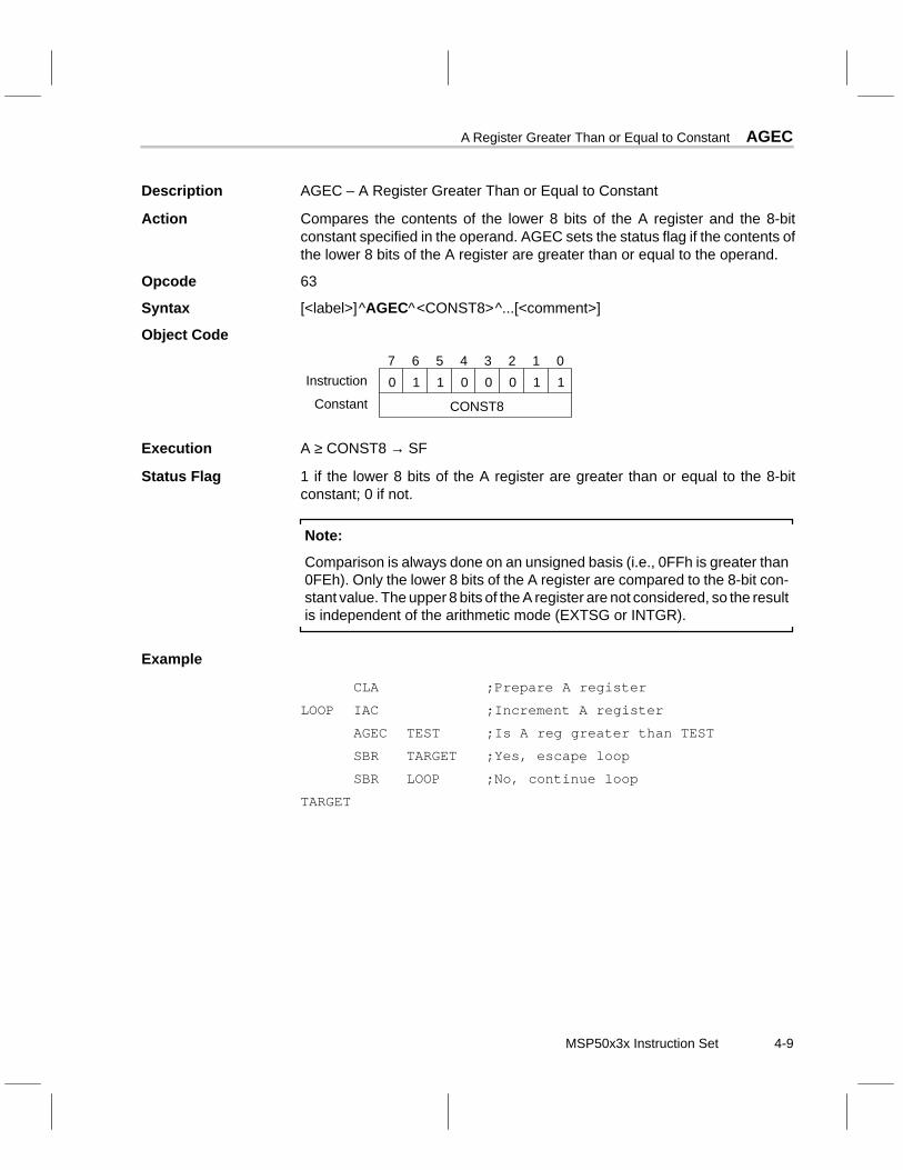
A Register Greater Than or Equal to Constant AGEC
4-9 MSP50x3x Instruction Set
Description AGEC – A Register Greater Than or Equal to Constant
Action Compares the contents of the lower 8 bits of the A register and the 8-bitconstant specified in the operand. AGEC sets the status flag if the contents ofthe lower 8 bits of the A register are greater than or equal to the operand.
Opcode 63
Syntax [<label>]^AGEC^<CONST8>^...[<comment>]
Object Code
34567 2 1 0
00110 0 1 1Instruction
CONST8Constant
Execution A ≥ CONST8 → SF
Status Flag 1 if the lower 8 bits of the A register are greater than or equal to the 8-bitconstant; 0 if not.
Note:
Comparison is always done on an unsigned basis (i.e., 0FFh is greater than0FEh). Only the lower 8 bits of the A register are compared to the 8-bit con-stant value. The upper 8 bits of the A register are not considered, so the resultis independent of the arithmetic mode (EXTSG or INTGR).
Example
CLA ;Prepare A register
LOOP IAC ;Increment A register
AGEC TEST ;Is A reg greater than TEST
SBR TARGET ;Yes, escape loop
SBR LOOP ;No, continue loop
TARGET
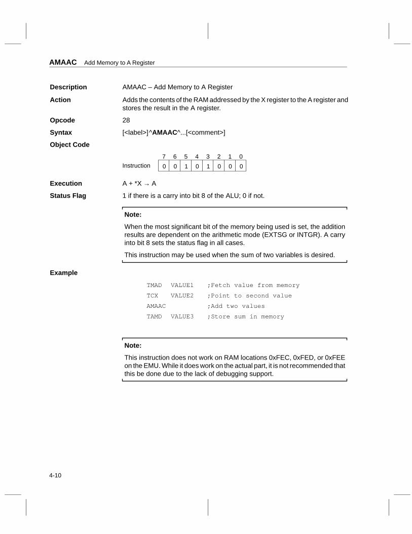
AMAAC Add Memory to A Register
4-10
Description AMAAC – Add Memory to A Register
Action Adds the contents of the RAM addressed by the X register to the A register andstores the result in the A register.
Opcode 28
Syntax [<label>]^AMAAC^...[<comment>]
Object Code
34567 2 1 0
10100 0 0 0Instruction
Execution A + *X → A
Status Flag 1 if there is a carry into bit 8 of the ALU; 0 if not.
Note:
When the most significant bit of the memory being used is set, the additionresults are dependent on the arithmetic mode (EXTSG or INTGR). A carryinto bit 8 sets the status flag in all cases.
This instruction may be used when the sum of two variables is desired.
Example
TMAD VALUE1 ;Fetch value from memory
TCX VALUE2 ;Point to second value
AMAAC ;Add two values
TAMD VALUE3 ;Store sum in memory
Note:
This instruction does not work on RAM locations 0xFEC, 0xFED, or 0xFEEon the EMU. While it does work on the actual part, it is not recommended thatthis be done due to the lack of debugging support.
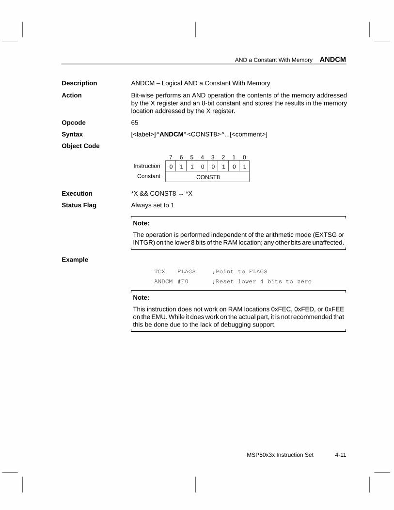
AND a Constant With Memory ANDCM
4-11 MSP50x3x Instruction Set
Description ANDCM – Logical AND a Constant With Memory
Action Bit-wise performs an AND operation the contents of the memory addressedby the X register and an 8-bit constant and stores the results in the memorylocation addressed by the X register.
Opcode 65
Syntax [<label>]^ANDCM^<CONST8>^...[<comment>]
Object Code
34567 2 1 0
00110 1 0 1Instruction
CONST8Constant
Execution *X && CONST8 → *X
Status Flag Always set to 1
Note:
The operation is performed independent of the arithmetic mode (EXTSG orINTGR) on the lower 8 bits of the RAM location; any other bits are unaffected.
Example
TCX FLAGS ;Point to FLAGS
ANDCM #F0 ;Reset lower 4 bits to zero
Note:
This instruction does not work on RAM locations 0xFEC, 0xFED, or 0xFEEon the EMU. While it does work on the actual part, it is not recommended thatthis be done due to the lack of debugging support.
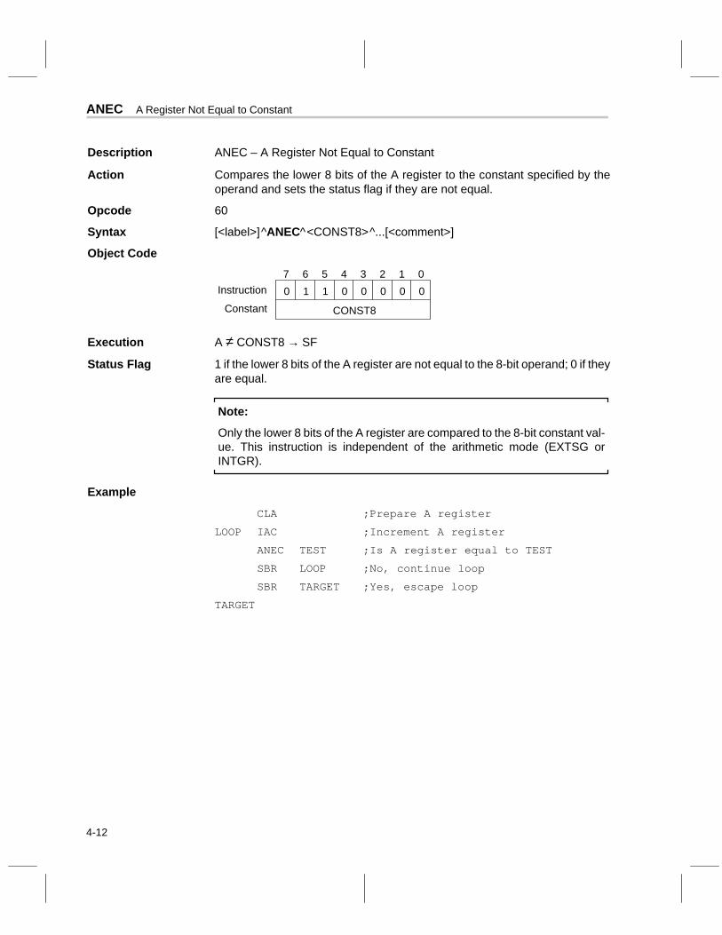
ANEC A Register Not Equal to Constant
4-12
Description ANEC – A Register Not Equal to Constant
Action Compares the lower 8 bits of the A register to the constant specified by theoperand and sets the status flag if they are not equal.
Opcode 60
Syntax [<label>]^ANEC^<CONST8>^...[<comment>]
Object Code
34567 2 1 0
00110 0 0 0Instruction
CONST8Constant
Execution A ≠ CONST8 → SF
Status Flag 1 if the lower 8 bits of the A register are not equal to the 8-bit operand; 0 if theyare equal.
Note:
Only the lower 8 bits of the A register are compared to the 8-bit constant val-ue. This instruction is independent of the arithmetic mode (EXTSG orINTGR).
Example
CLA ;Prepare A register
LOOP IAC ;Increment A register
ANEC TEST ;Is A register equal to TEST
SBR LOOP ;No, continue loop
SBR TARGET ;Yes, escape loop
TARGET
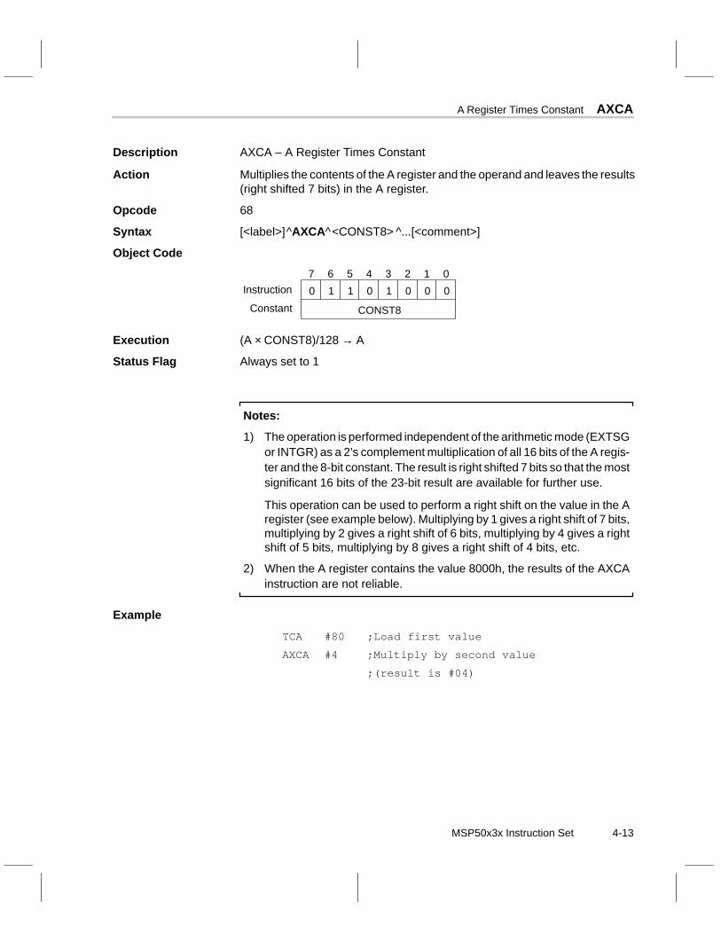
A Register Times Constant AXCA
4-13 MSP50x3x Instruction Set
Description AXCA – A Register Times Constant
Action Multiplies the contents of the A register and the operand and leaves the results(right shifted 7 bits) in the A register.
Opcode 68
Syntax [<label>]^AXCA^<CONST8> ^...[<comment>]
Object Code
34567 2 1 0
10110 0 0 0Instruction
CONST8Constant
Execution (A × CONST8)/128 → A
Status Flag Always set to 1
Notes:
1) The operation is performed independent of the arithmetic mode (EXTSGor INTGR) as a 2’s complement multiplication of all 16 bits of the A regis-ter and the 8-bit constant. The result is right shifted 7 bits so that the mostsignificant 16 bits of the 23-bit result are available for further use.
This operation can be used to perform a right shift on the value in the Aregister (see example below). Multiplying by 1 gives a right shift of 7 bits,multiplying by 2 gives a right shift of 6 bits, multiplying by 4 gives a rightshift of 5 bits, multiplying by 8 gives a right shift of 4 bits, etc.
2) When the A register contains the value 8000h, the results of the AXCAinstruction are not reliable.
Example
TCA #80 ;Load first value
AXCA #4 ;Multiply by second value
;(result is #04)
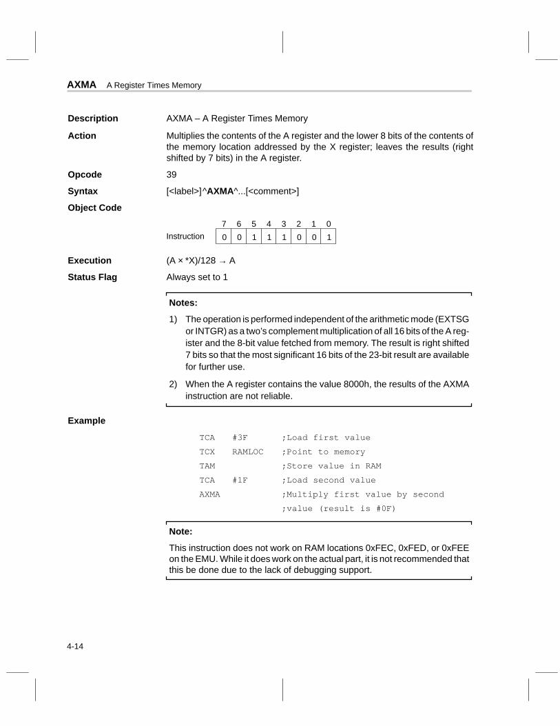
AXMA A Register Times Memory
4-14
Description AXMA – A Register Times Memory
Action Multiplies the contents of the A register and the lower 8 bits of the contents ofthe memory location addressed by the X register; leaves the results (rightshifted by 7 bits) in the A register.
Opcode 39
Syntax [<label>]^AXMA^...[<comment>]
Object Code
34567 2 1 0
11100 0 0 1Instruction
Execution (A × *X)/128 → A
Status Flag Always set to 1
Notes:
1) The operation is performed independent of the arithmetic mode (EXTSGor INTGR) as a two’s complement multiplication of all 16 bits of the A reg-ister and the 8-bit value fetched from memory. The result is right shifted7 bits so that the most significant 16 bits of the 23-bit result are availablefor further use.
2) When the A register contains the value 8000h, the results of the AXMAinstruction are not reliable.
Example
TCA #3F ;Load first value
TCX RAMLOC ;Point to memory
TAM ;Store value in RAM
TCA #1F ;Load second value
AXMA ;Multiply first value by second
;value (result is #0F)
Note:
This instruction does not work on RAM locations 0xFEC, 0xFED, or 0xFEEon the EMU. While it does work on the actual part, it is not recommended thatthis be done due to the lack of debugging support.
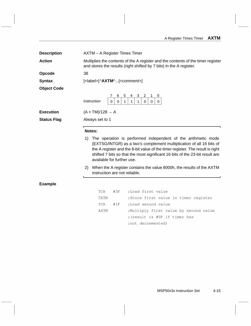
A Register Times Timer AXTM
4-15 MSP50x3x Instruction Set
Description AXTM – A Register Times Timer
Action Multiplies the contents of the A register and the contents of the timer registerand stores the results (right shifted by 7 bits) in the A register.
Opcode 38
Syntax [<label>]^AXTM^...[<comment>]
Object Code
34567 2 1 0
11100 0 0 0Instruction
Execution (A × TM)/128 → A
Status Flag Always set to 1
Notes:
1) The operation is performed independent of the arithmetic mode(EXTSG/INTGR) as a two’s complement multiplication of all 16 bits ofthe A register and the 8-bit value of the timer register. The result is rightshifted 7 bits so that the most significant 16 bits of the 23-bit result areavailable for further use.
2) When the A register contains the value 8000h, the results of the AXTMinstruction are not reliable.
Example
TCA #3F ;Load first value
TATM ;Store first value in timer register
TCA #1F ;Load second value
AXTM ;Multiply first value by second value
;(result is #0F if timer has
;not decremented)
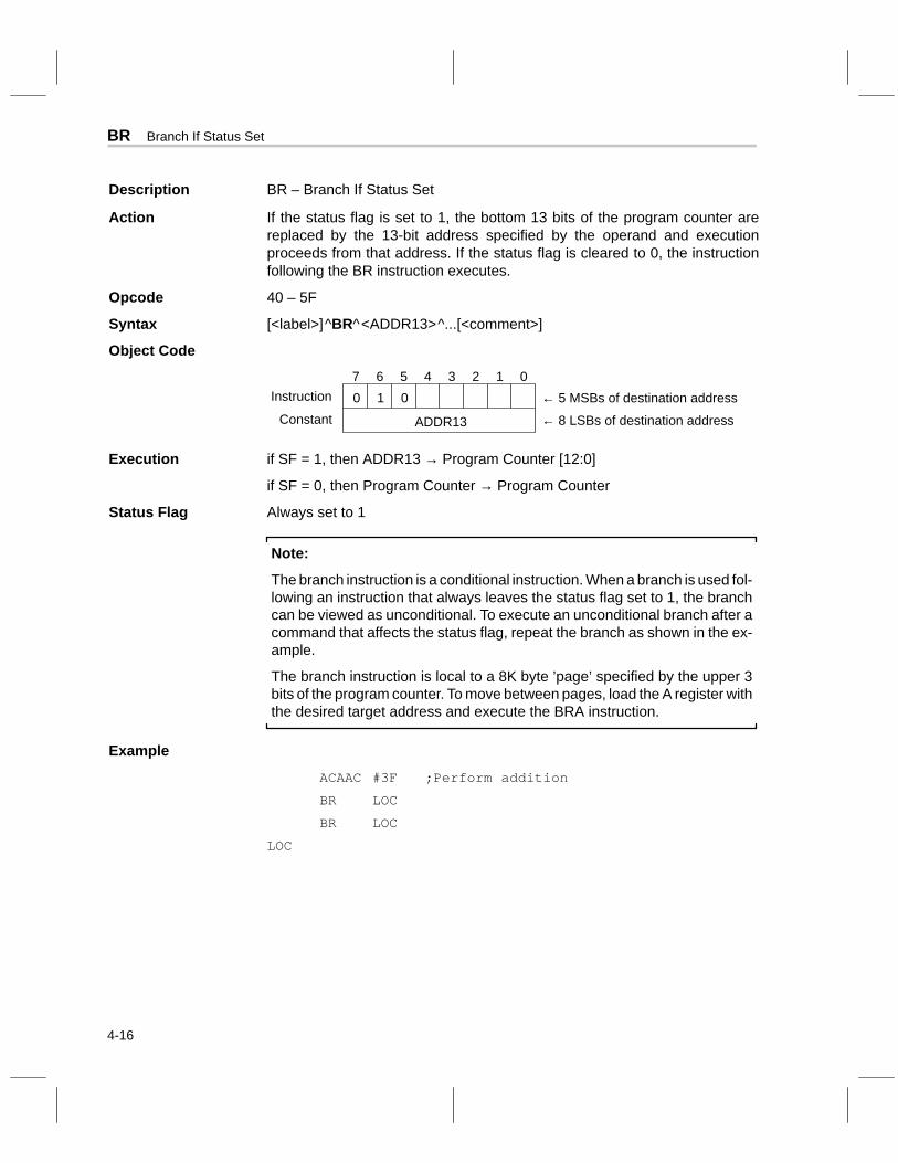
BR Branch If Status Set
4-16
Description BR – Branch If Status Set
Action If the status flag is set to 1, the bottom 13 bits of the program counter arereplaced by the 13-bit address specified by the operand and executionproceeds from that address. If the status flag is cleared to 0, the instructionfollowing the BR instruction executes.
Opcode 40 – 5F
Syntax [<label>]^BR^<ADDR13>^...[<comment>]
Object Code
34567 2 1 0
010Instruction
ADDR13Constant
← 5 MSBs of destination address
← 8 LSBs of destination address
Execution if SF = 1, then ADDR13 → Program Counter [12:0]
if SF = 0, then Program Counter → Program Counter
Status Flag Always set to 1
Note:
The branch instruction is a conditional instruction. When a branch is used fol-lowing an instruction that always leaves the status flag set to 1, the branchcan be viewed as unconditional. To execute an unconditional branch after acommand that affects the status flag, repeat the branch as shown in the ex-ample.
The branch instruction is local to a 8K byte ’page’ specified by the upper 3bits of the program counter. To move between pages, load the A register withthe desired target address and execute the BRA instruction.
Example
ACAAC #3F ;Perform addition
BR LOC
BR LOC
LOC
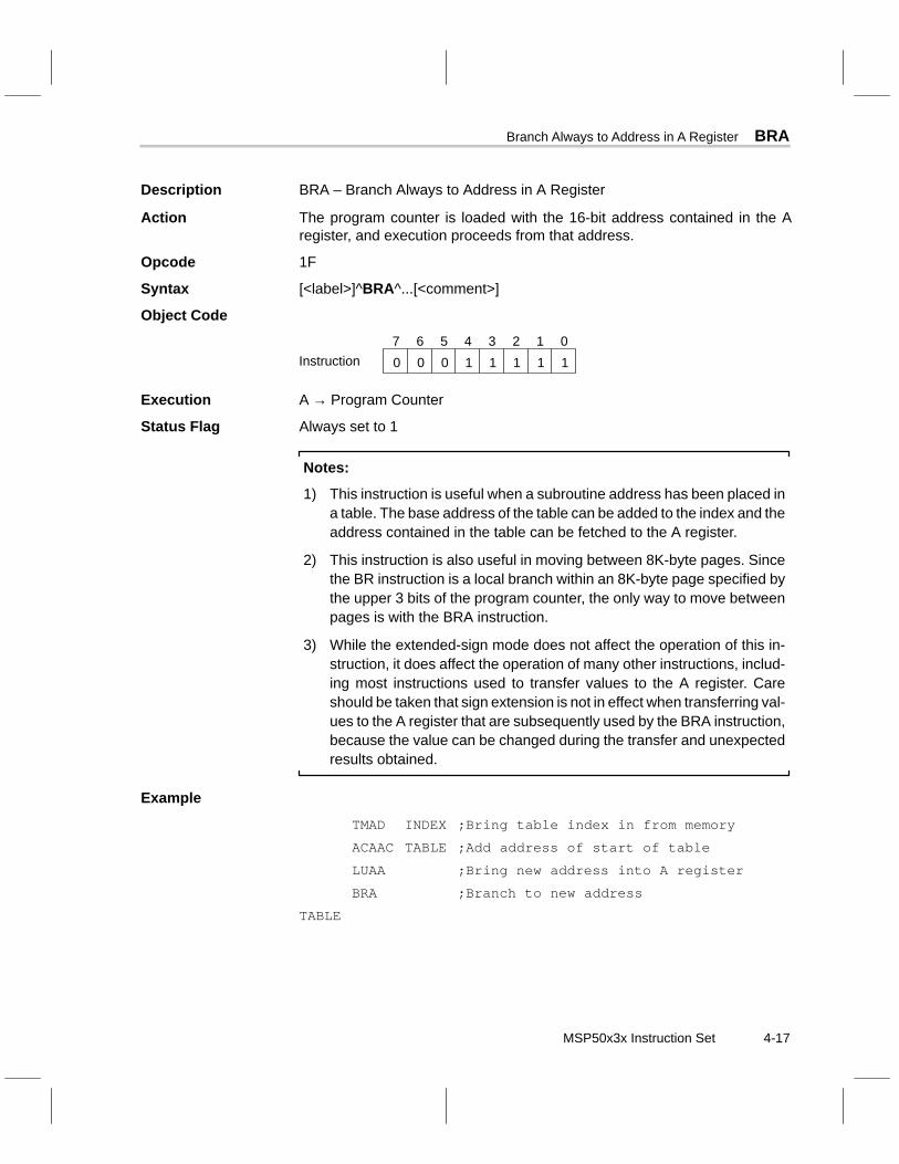
Branch Always to Address in A Register BRA
4-17 MSP50x3x Instruction Set
Description BRA – Branch Always to Address in A Register
Action The program counter is loaded with the 16-bit address contained in the Aregister, and execution proceeds from that address.
Opcode 1F
Syntax [<label>]^BRA^...[<comment>]
Object Code
34567 2 1 0
11000 1 1 1Instruction
Execution A → Program Counter
Status Flag Always set to 1
Notes:
1) This instruction is useful when a subroutine address has been placed ina table. The base address of the table can be added to the index and theaddress contained in the table can be fetched to the A register.
2) This instruction is also useful in moving between 8K-byte pages. Sincethe BR instruction is a local branch within an 8K-byte page specified bythe upper 3 bits of the program counter, the only way to move betweenpages is with the BRA instruction.
3) While the extended-sign mode does not affect the operation of this in-struction, it does affect the operation of many other instructions, includ-ing most instructions used to transfer values to the A register. Careshould be taken that sign extension is not in effect when transferring val-ues to the A register that are subsequently used by the BRA instruction,because the value can be changed during the transfer and unexpectedresults obtained.
Example
TMAD INDEX ;Bring table index in from memory
ACAAC TABLE ;Add address of start of table
LUAA ;Bring new address into A register
BRA ;Branch to new address
TABLE
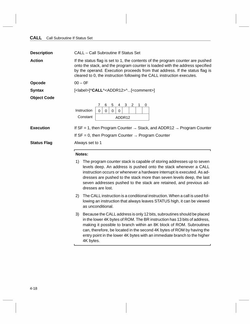
CALL Call Subroutine If Status Set
4-18
Description CALL – Call Subroutine If Status Set
Action If the status flag is set to 1, the contents of the program counter are pushedonto the stack, and the program counter is loaded with the address specifiedby the operand. Execution proceeds from that address. If the status flag iscleared to 0, the instruction following the CALL instruction executes.
Opcode 00 – 0F
Syntax [<label>]^CALL^<ADDR12>^...[<comment>]
Object Code
34567 2 1 0
0000Instruction
ADDR12Constant
Execution If SF = 1, then Program Counter → Stack, and ADDR12 → Program Counter
If SF = 0, then Program Counter → Program Counter
Status Flag Always set to 1
Notes:
1) The program counter stack is capable of storing addresses up to sevenlevels deep. An address is pushed onto the stack whenever a CALLinstruction occurs or whenever a hardware interrupt is executed. As ad-dresses are pushed to the stack more than seven levels deep, the lastseven addresses pushed to the stack are retained, and previous ad-dresses are lost.
2) The CALL instruction is a conditional instruction. When a call is used fol-lowing an instruction that always leaves STATUS high, it can be viewedas unconditional.
3) Because the CALL address is only 12 bits, subroutines should be placedin the lower 4K bytes of ROM. The BR instruction has 13 bits of address,making it possible to branch within an 8K block of ROM. Subroutinescan, therefore, be located in the second 4K bytes of ROM by having theentry point in the lower 4K bytes with an immediate branch to the higher4K bytes.
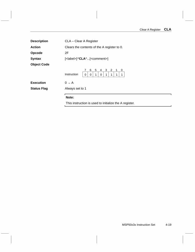
Clear A Register CLA
4-19 MSP50x3x Instruction Set
Description CLA – Clear A Register
Action Clears the contents of the A register to 0.
Opcode 2F
Syntax [<label>]^CLA^...[<comment>]
Object Code
34567 2 1 0
10100 1 1 1Instruction
Execution 0 → A
Status Flag Always set to 1
Note:
This instruction is used to initialize the A register.
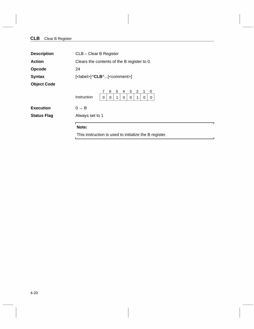
CLB Clear B Register
4-20
Description CLB – Clear B Register
Action Clears the contents of the B register to 0.
Opcode 24
Syntax [<label>]^CLB^...[<comment>]
Object Code
34567 2 1 0
00100 1 0 0Instruction
Execution 0 → B
Status Flag Always set to 1
Note:
This instruction is used to initialize the B register.

Clear X Register CLX
4-21 MSP50x3x Instruction Set
Description CLX – Clear X Register
Action Clears the contents of the X register to 0.
Opcode 20
Syntax [<label>]^CLX^...[<comment>]
Object Code
34567 2 1 0
00100 0 0 0Instruction
Execution 0 → X
Status Flag Always set to 1
Note:
This instruction is used to initialize the X register.
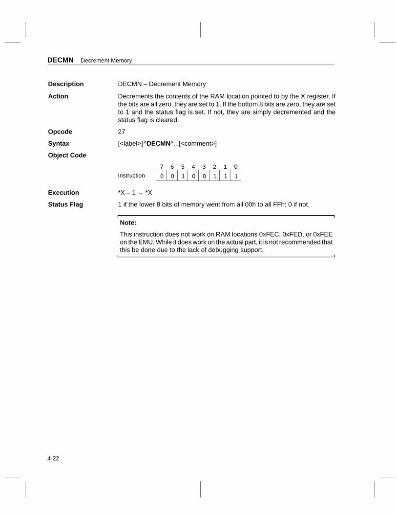
DECMN Decrement Memory
4-22
Description DECMN – Decrement Memory
Action Decrements the contents of the RAM location pointed to by the X register. Ifthe bits are all zero, they are set to 1. If the bottom 8 bits are zero, they are setto 1 and the status flag is set. If not, they are simply decremented and thestatus flag is cleared.
Opcode 27
Syntax [<label>]^DECMN^...[<comment>]
Object Code
34567 2 1 0
00100 1 1 1Instruction
Execution *X – 1 → *X
Status Flag 1 if the lower 8 bits of memory went from all 00h to all FFh; 0 if not.
Note:
This instruction does not work on RAM locations 0xFEC, 0xFED, or 0xFEEon the EMU. While it does work on the actual part, it is not recommended thatthis be done due to the lack of debugging support.
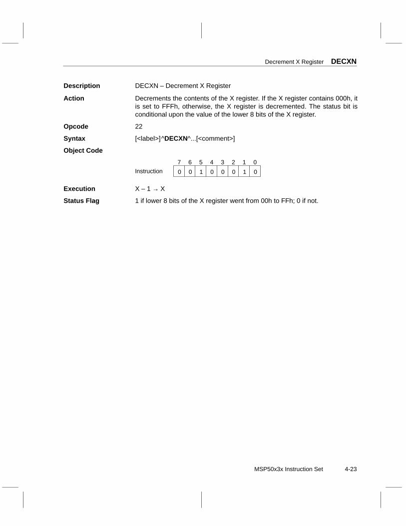
Decrement X Register DECXN
4-23 MSP50x3x Instruction Set
Description DECXN – Decrement X Register
Action Decrements the contents of the X register. If the X register contains 000h, itis set to FFFh, otherwise, the X register is decremented. The status bit isconditional upon the value of the lower 8 bits of the X register.
Opcode 22
Syntax [<label>]^DECXN^...[<comment>]
Object Code
34567 2 1 0
00100 0 1 0Instruction
Execution X – 1 → X
Status Flag 1 if lower 8 bits of the X register went from 00h to FFh; 0 if not.
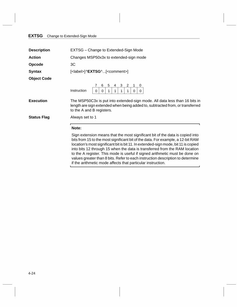
EXTSG Change to Extended-Sign Mode
4-24
Description EXTSG – Change to Extended-Sign Mode
Action Changes MSP50x3x to extended-sign mode
Opcode 3C
Syntax [<label>]^EXTSG^...[<comment>]
Object Code
34567 2 1 0
11100 1 0 0Instruction
Execution The MSP50C3x is put into extended-sign mode. All data less than 16 bits inlength are sign extended when being added to, subtracted from, or transferredto the A and B registers.
Status Flag Always set to 1
Note:
Sign extension means that the most significant bit of the data is copied intobits from 15 to the most significant bit of the data. For example, a 12-bit RAMlocation’s most significant bit is bit 11. In extended-sign mode, bit 11 is copiedinto bits 12 through 15 when the data is transferred from the RAM locationto the A register. This mode is useful if signed arithmetic must be done onvalues greater than 8 bits. Refer to each instruction description to determineif the arithmetic mode affects that particular instruction.
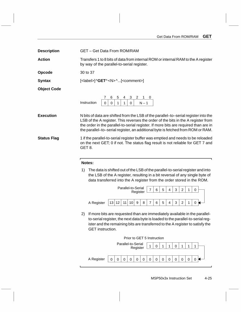
Get Data From ROM/RAM GET
4-25 MSP50x3x Instruction Set
Description GET – Get Data From ROM/RAM
Action Transfers 1 to 8 bits of data from internal ROM or internal RAM to the A registerby way of the parallel-to-serial register.
Opcode 30 to 37
Syntax [<label>]^GET^<N>^...[<comment>]
Object Code
34567 2 1 0
01100 N – 1Instruction
Execution N bits of data are shifted from the LSB of the parallel–to–serial register into theLSB of the A register. This reverses the order of the bits in the A register fromthe order in the parallel-to-serial register. If more bits are required than are inthe parallel–to–serial register, an additional byte is fetched from ROM or RAM.
Status Flag 1 if the parallel-to-serial register buffer was emptied and needs to be reloadedon the next GET; 0 if not. The status flag result is not reliable for GET 7 andGET 8.
Notes:
13 12 11 10 9 8 34567 2 1 0
34567 2 1 0
A Register
Parallel-to-SerialRegister
1) The data is shifted out of the LSB of the parallel-to-serial register and intothe LSB of the A register, resulting in a bit reversal of any single byte ofdata transferred into the A register from the order stored in the ROM.
2) If more bits are requested than are immediately available in the parallel-to-serial register, the next data byte is loaded to the parallel-to-serial reg-ister and the remaining bits are transferred to the A register to satisfy theGET instruction.
0 0 0 0 0 0 00000 0 0 0
01101 1 1 1
A Register
Parallel-to-SerialRegister
Prior to GET 5 Instruction
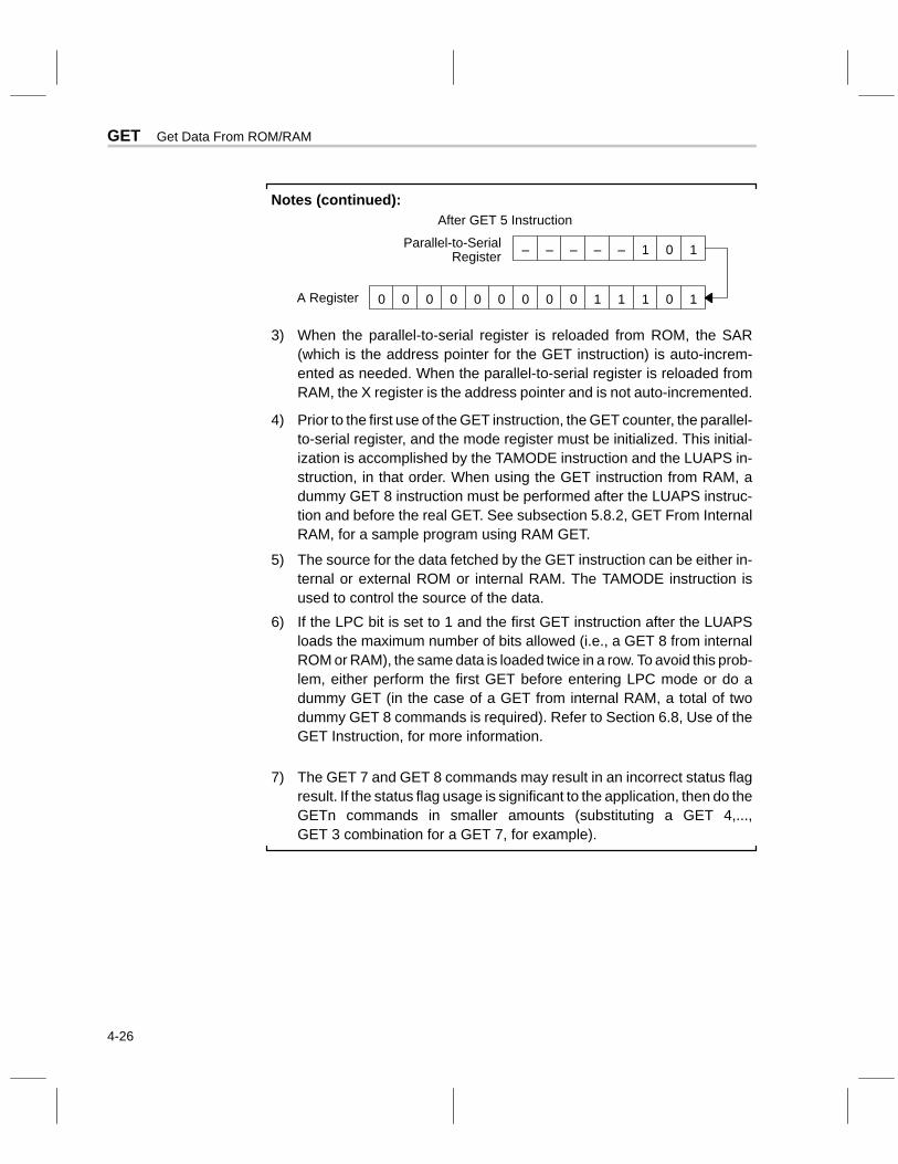
GET Get Data From ROM/RAM
4-26
Notes (continued):
3) When the parallel-to-serial register is reloaded from ROM, the SAR(which is the address pointer for the GET instruction) is auto-increm-ented as needed. When the parallel-to-serial register is reloaded fromRAM, the X register is the address pointer and is not auto-incremented.
After GET 5 Instruction
0 0 0 0 0 0 11000 1 0 1
––––– 1 0 1
A Register
Parallel-to-SerialRegister
4) Prior to the first use of the GET instruction, the GET counter, the parallel-to-serial register, and the mode register must be initialized. This initial-ization is accomplished by the TAMODE instruction and the LUAPS in-struction, in that order. When using the GET instruction from RAM, adummy GET 8 instruction must be performed after the LUAPS instruc-tion and before the real GET. See subsection 5.8.2, GET From InternalRAM, for a sample program using RAM GET.
5) The source for the data fetched by the GET instruction can be either in-ternal or external ROM or internal RAM. The TAMODE instruction isused to control the source of the data.
6) If the LPC bit is set to 1 and the first GET instruction after the LUAPSloads the maximum number of bits allowed (i.e., a GET 8 from internalROM or RAM), the same data is loaded twice in a row. To avoid this prob-lem, either perform the first GET before entering LPC mode or do adummy GET (in the case of a GET from internal RAM, a total of twodummy GET 8 commands is required). Refer to Section 6.8, Use of theGET Instruction, for more information.
7) The GET 7 and GET 8 commands may result in an incorrect status flagresult. If the status flag usage is significant to the application, then do theGETn commands in smaller amounts (substituting a GET 4,...,GET 3 combination for a GET 7, for example).
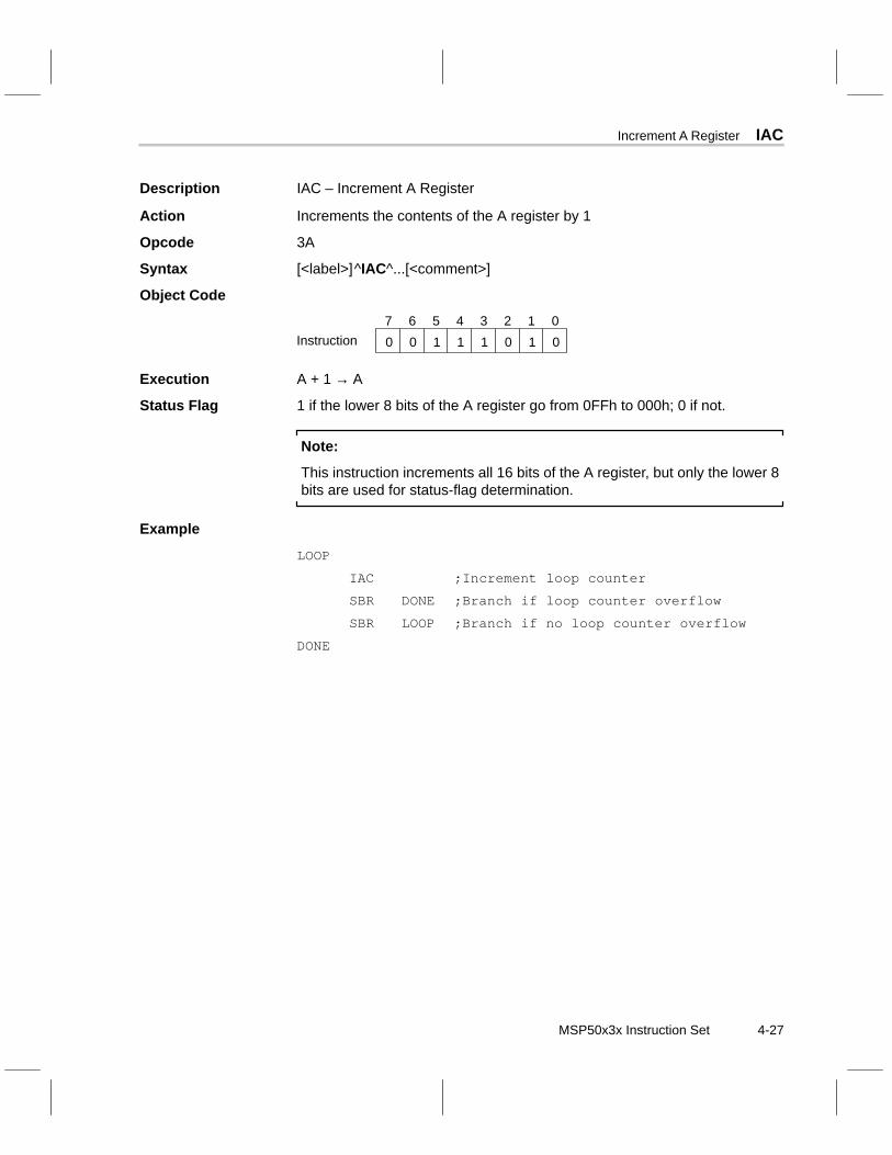
Increment A Register IAC
4-27 MSP50x3x Instruction Set
Description IAC – Increment A Register
Action Increments the contents of the A register by 1
Opcode 3A
Syntax [<label>]^IAC^...[<comment>]
Object Code
34567 2 1 0
11100 0 1 0Instruction
Execution A + 1 → A
Status Flag 1 if the lower 8 bits of the A register go from 0FFh to 000h; 0 if not.
Note:
This instruction increments all 16 bits of the A register, but only the lower 8bits are used for status-flag determination.
Example
LOOP
IAC ;Increment loop counter
SBR DONE ;Branch if loop counter overflow
SBR LOOP ;Branch if no loop counter overflow
DONE
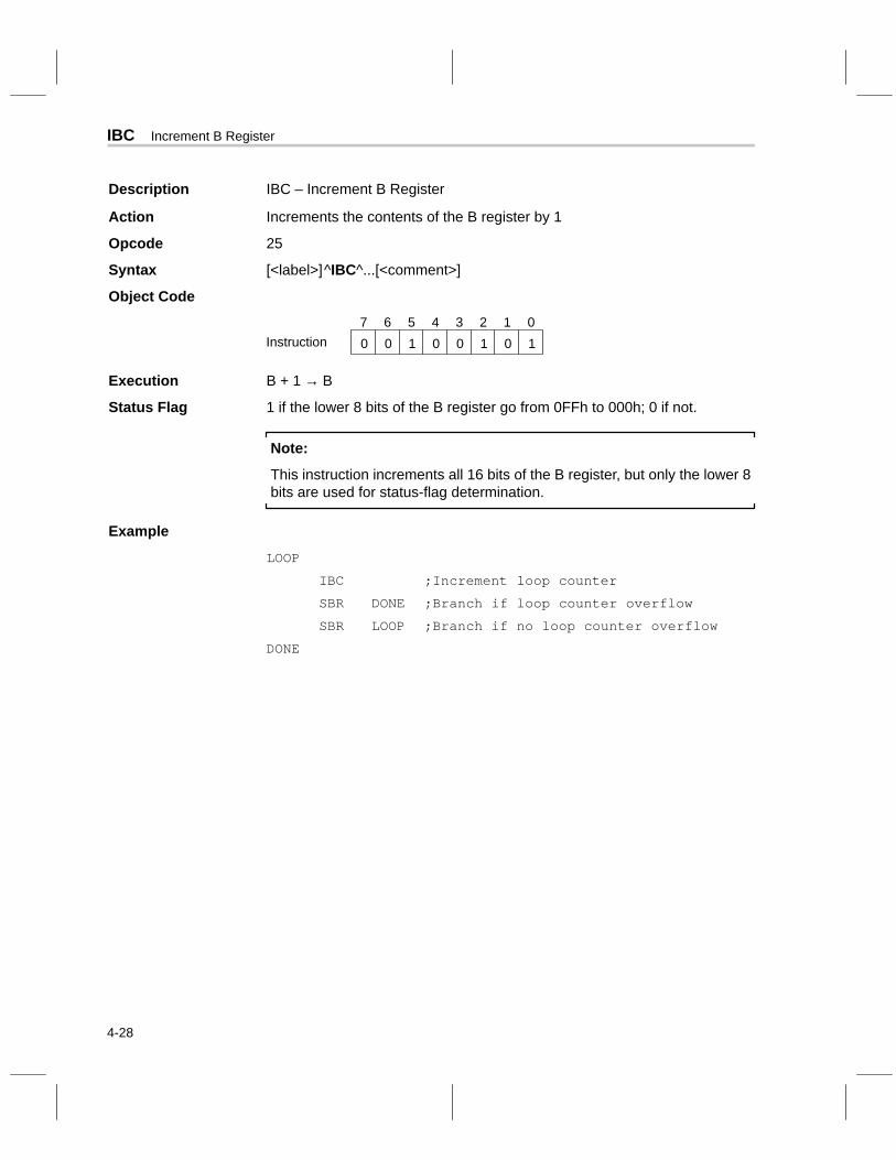
IBC Increment B Register
4-28
Description IBC – Increment B Register
Action Increments the contents of the B register by 1
Opcode 25
Syntax [<label>]^IBC^...[<comment>]
Object Code
34567 2 1 0
00100 1 0 1Instruction
Execution B + 1 → B
Status Flag 1 if the lower 8 bits of the B register go from 0FFh to 000h; 0 if not.
Note:
This instruction increments all 16 bits of the B register, but only the lower 8bits are used for status-flag determination.
Example
LOOP
IBC ;Increment loop counter
SBR DONE ;Branch if loop counter overflow
SBR LOOP ;Branch if no loop counter overflow
DONE
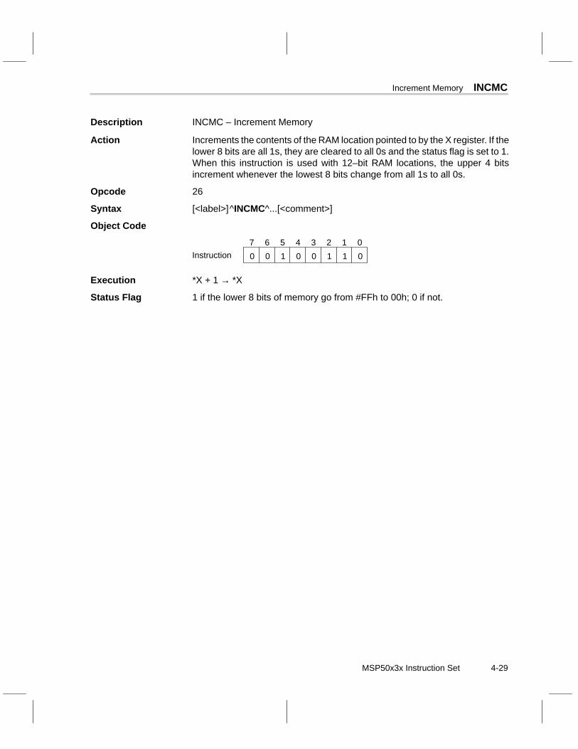
Increment Memory INCMC
4-29 MSP50x3x Instruction Set
Description INCMC – Increment Memory
Action Increments the contents of the RAM location pointed to by the X register. If thelower 8 bits are all 1s, they are cleared to all 0s and the status flag is set to 1.When this instruction is used with 12–bit RAM locations, the upper 4 bitsincrement whenever the lowest 8 bits change from all 1s to all 0s.
Opcode 26
Syntax [<label>]^INCMC^...[<comment>]
Object Code
34567 2 1 0
00100 1 1 0Instruction
Execution *X + 1 → *X
Status Flag 1 if the lower 8 bits of memory go from #FFh to 00h; 0 if not.
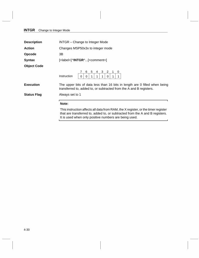
INTGR Change to Integer Mode
4-30
Description INTGR – Change to Integer Mode
Action Changes MSP50x3x to integer mode
Opcode 3B
Syntax [<label>]^INTGR^...[<comment>]
Object Code
34567 2 1 0
11100 0 1 1Instruction
Execution The upper bits of data less than 16 bits in length are 0 filled when beingtransferred to, added to, or subtracted from the A and B registers.
Status Flag Always set to 1
Note:
This instruction affects all data from RAM, the X register, or the timer registerthat are transferred to, added to, or subtracted from the A and B registers.It is used when only positive numbers are being used.
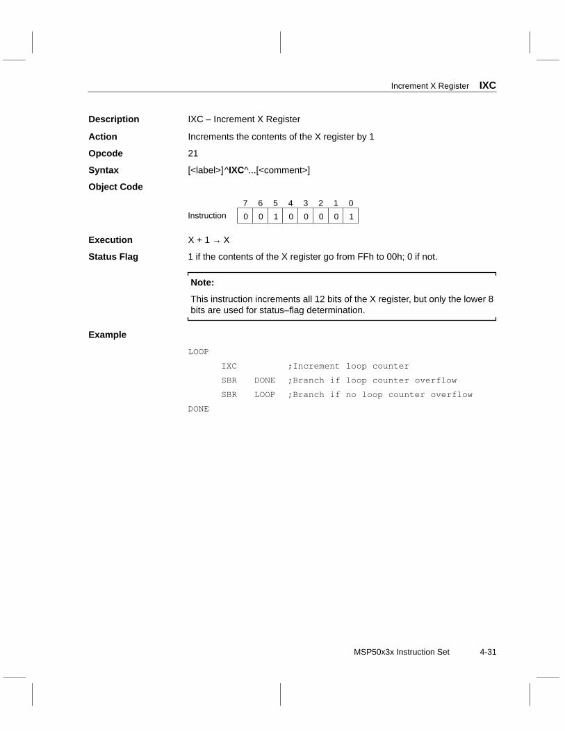
Increment X Register IXC
4-31 MSP50x3x Instruction Set
Description IXC – Increment X Register
Action Increments the contents of the X register by 1
Opcode 21
Syntax [<label>]^IXC^...[<comment>]
Object Code
34567 2 1 0
00100 0 0 1Instruction
Execution X + 1 → X
Status Flag 1 if the contents of the X register go from FFh to 00h; 0 if not.
Note:
This instruction increments all 12 bits of the X register, but only the lower 8bits are used for status–flag determination.
Example
LOOP
IXC ;Increment loop counter
SBR DONE ;Branch if loop counter overflow
SBR LOOP ;Branch if no loop counter overflow
DONE
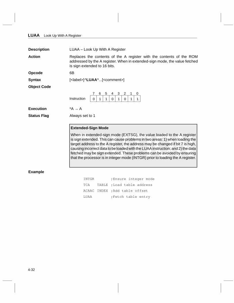
LUAA Look Up With A Register
4-32
Description LUAA – Look Up With A Register
Action Replaces the contents of the A register with the contents of the ROMaddressed by the A register. When in extended-sign mode, the value fetchedis sign extended to 16 bits.
Opcode 6B
Syntax [<label>]^LUAA^...[<comment>]
Object Code
34567 2 1 0
10110 0 1 1Instruction
Execution *A → A
Status Flag Always set to 1
Extended-Sign Mode
When in extended-sign mode (EXTSG), the value loaded to the A registeris sign extended. This can cause problems in two areas: 1) when loading thetarget address to the A register, the address may be changed if bit 7 is high,causing incorrect data to be loaded with the LUAA instruction; and 2) the datafetched may be sign extended. These problems can be avoided by ensuringthat the processor is in integer mode (INTGR) prior to loading the A register.
Example
INTGR ;Ensure integer mode
TCA TABLE ;Load table address
ACAAC INDEX ;Add table offset
LUAA ;Fetch table entry
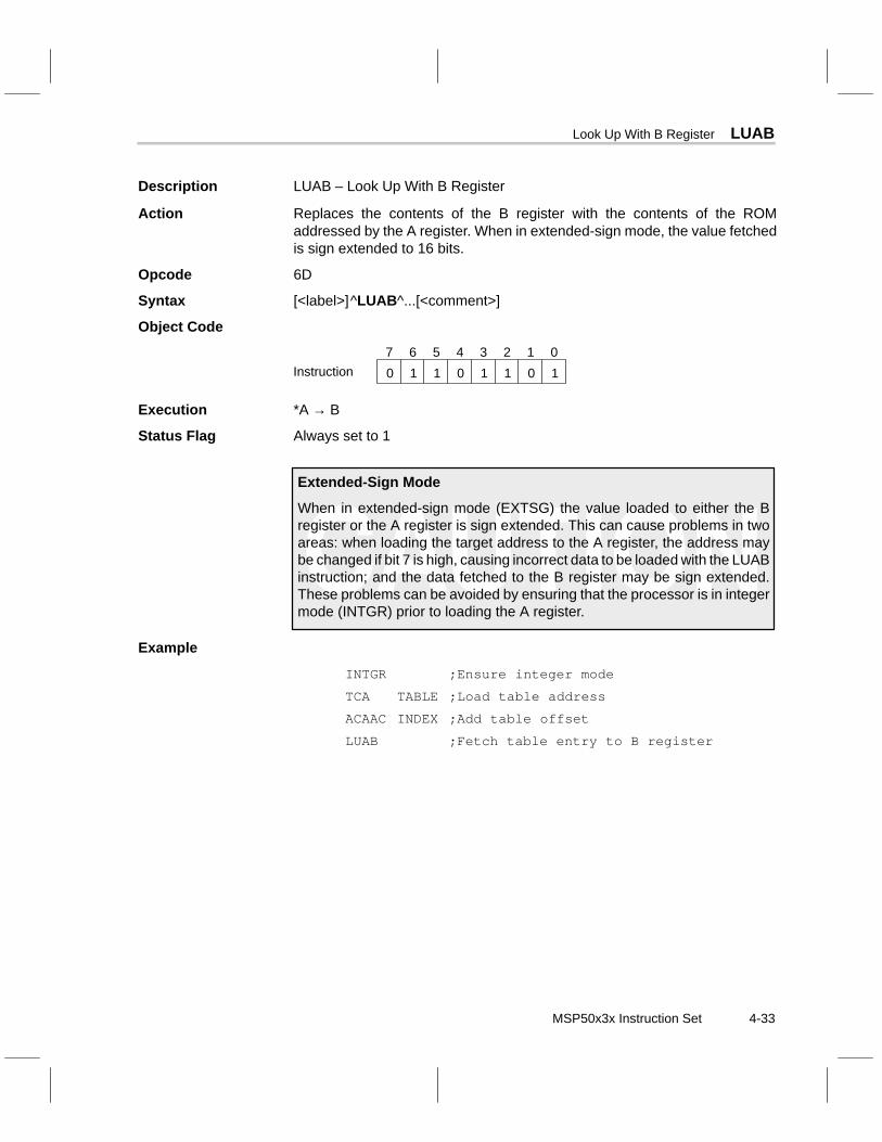
Look Up With B Register LUAB
4-33 MSP50x3x Instruction Set
Description LUAB – Look Up With B Register
Action Replaces the contents of the B register with the contents of the ROMaddressed by the A register. When in extended-sign mode, the value fetchedis sign extended to 16 bits.
Opcode 6D
Syntax [<label>]^LUAB^...[<comment>]
Object Code
34567 2 1 0
10110 1 0 1Instruction
Execution *A → B
Status Flag Always set to 1
Extended-Sign Mode
When in extended-sign mode (EXTSG) the value loaded to either the Bregister or the A register is sign extended. This can cause problems in twoareas: when loading the target address to the A register, the address maybe changed if bit 7 is high, causing incorrect data to be loaded with the LUABinstruction; and the data fetched to the B register may be sign extended.These problems can be avoided by ensuring that the processor is in integermode (INTGR) prior to loading the A register.
Example
INTGR ;Ensure integer mode
TCA TABLE ;Load table address
ACAAC INDEX ;Add table offset
LUAB ;Fetch table entry to B register
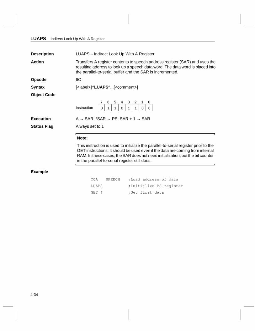
LUAPS Indirect Look Up With A Register
4-34
Description LUAPS – Indirect Look Up With A Register
Action Transfers A register contents to speech address register (SAR) and uses theresulting address to look up a speech data word. The data word is placed intothe parallel-to-serial buffer and the SAR is incremented.
Opcode 6C
Syntax [<label>]^LUAPS^...[<comment>]
Object Code
34567 2 1 0
10110 1 0 0Instruction
Execution A → SAR; *SAR → PS; SAR + 1 → SAR
Status Flag Always set to 1
Note:
This instruction is used to initialize the parallel-to-serial register prior to theGET instructions. It should be used even if the data are coming from internalRAM. In these cases, the SAR does not need initialization, but the bit counterin the parallel-to-serial register still does.
Example
TCA SPEECH ;Load address of data
LUAPS ;Initialize PS register
GET 4 ;Get first data
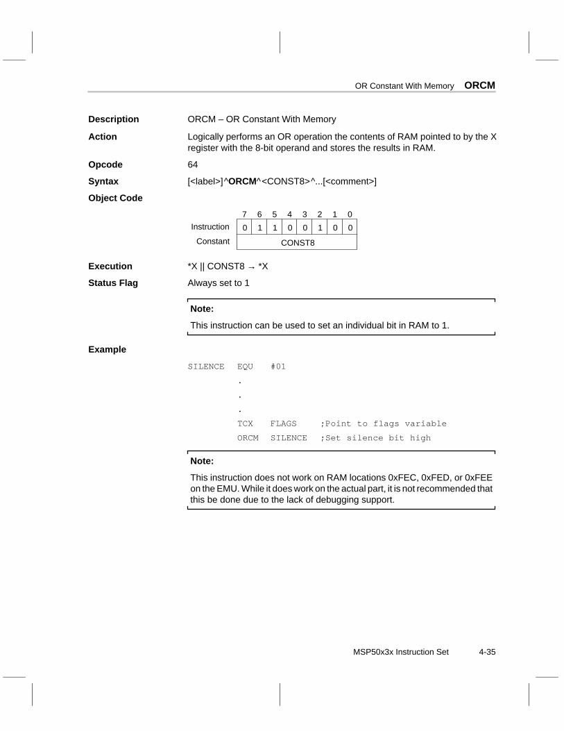
OR Constant With Memory ORCM
4-35 MSP50x3x Instruction Set
Description ORCM – OR Constant With Memory
Action Logically performs an OR operation the contents of RAM pointed to by the Xregister with the 8-bit operand and stores the results in RAM.
Opcode 64
Syntax [<label>]^ORCM^<CONST8>^...[<comment>]
Object Code
34567 2 1 0
00110 1 0 0Instruction
CONST8Constant
Execution *X || CONST8 → *X
Status Flag Always set to 1
Note:
This instruction can be used to set an individual bit in RAM to 1.
Example
SILENCE EQU #01
.
.
.
TCX FLAGS ;Point to flags variable
ORCM SILENCE ;Set silence bit high
Note:
This instruction does not work on RAM locations 0xFEC, 0xFED, or 0xFEEon the EMU. While it does work on the actual part, it is not recommended thatthis be done due to the lack of debugging support.
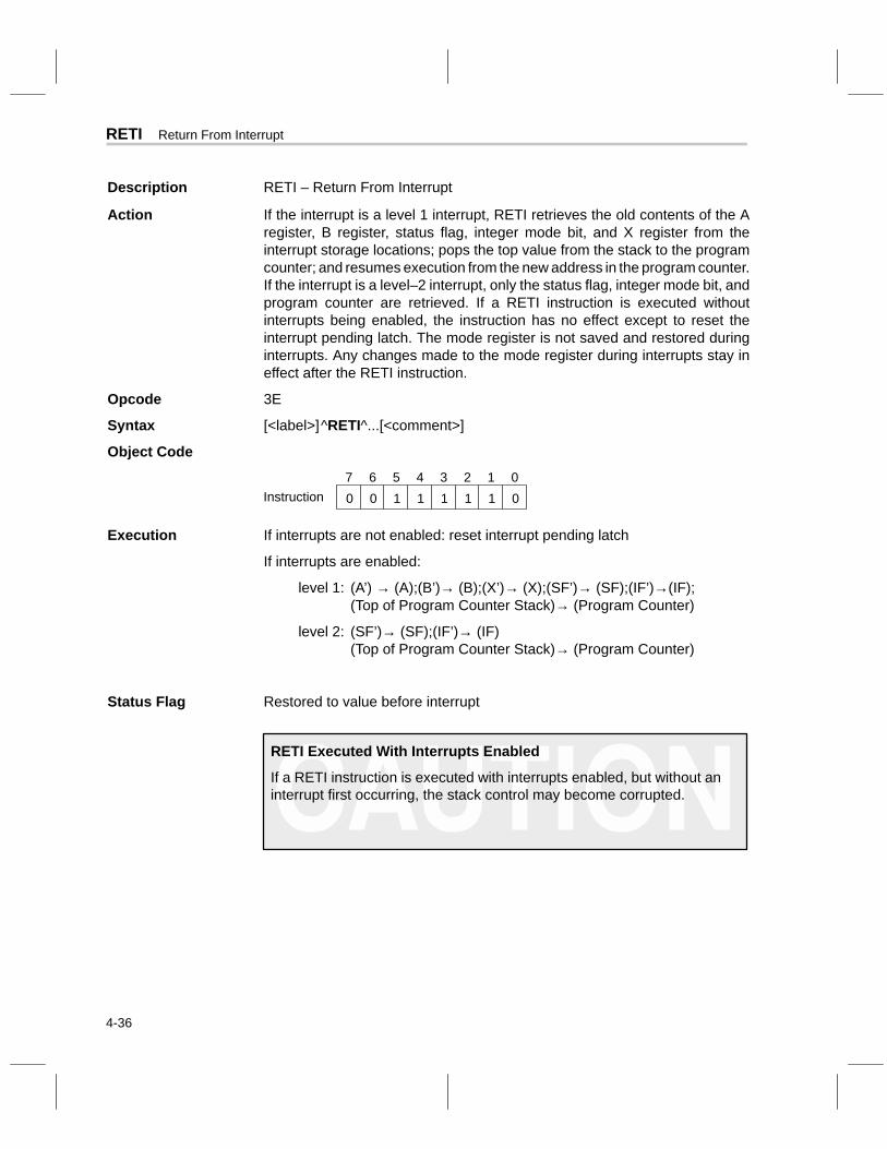
RETI Return From Interrupt
4-36
Description RETI – Return From Interrupt
Action If the interrupt is a level 1 interrupt, RETI retrieves the old contents of the Aregister, B register, status flag, integer mode bit, and X register from theinterrupt storage locations; pops the top value from the stack to the programcounter; and resumes execution from the new address in the program counter.If the interrupt is a level–2 interrupt, only the status flag, integer mode bit, andprogram counter are retrieved. If a RETI instruction is executed withoutinterrupts being enabled, the instruction has no effect except to reset theinterrupt pending latch. The mode register is not saved and restored duringinterrupts. Any changes made to the mode register during interrupts stay ineffect after the RETI instruction.
Opcode 3E
Syntax [<label>]^RETI^...[<comment>]
Object Code
34567 2 1 0
11100 1 1 0Instruction
Execution If interrupts are not enabled: reset interrupt pending latch
If interrupts are enabled:
level 1: (A’) → (A);(B’)→ (B);(X’)→ (X);(SF’)→ (SF);(IF’)→(IF); (Top of Program Counter Stack)→ (Program Counter)
level 2: (SF’)→ (SF);(IF’)→ (IF) (Top of Program Counter Stack)→ (Program Counter)
Status Flag Restored to value before interrupt
RETI Executed With Interrupts Enabled
If a RETI instruction is executed with interrupts enabled, but without aninterrupt first occurring, the stack control may become corrupted.
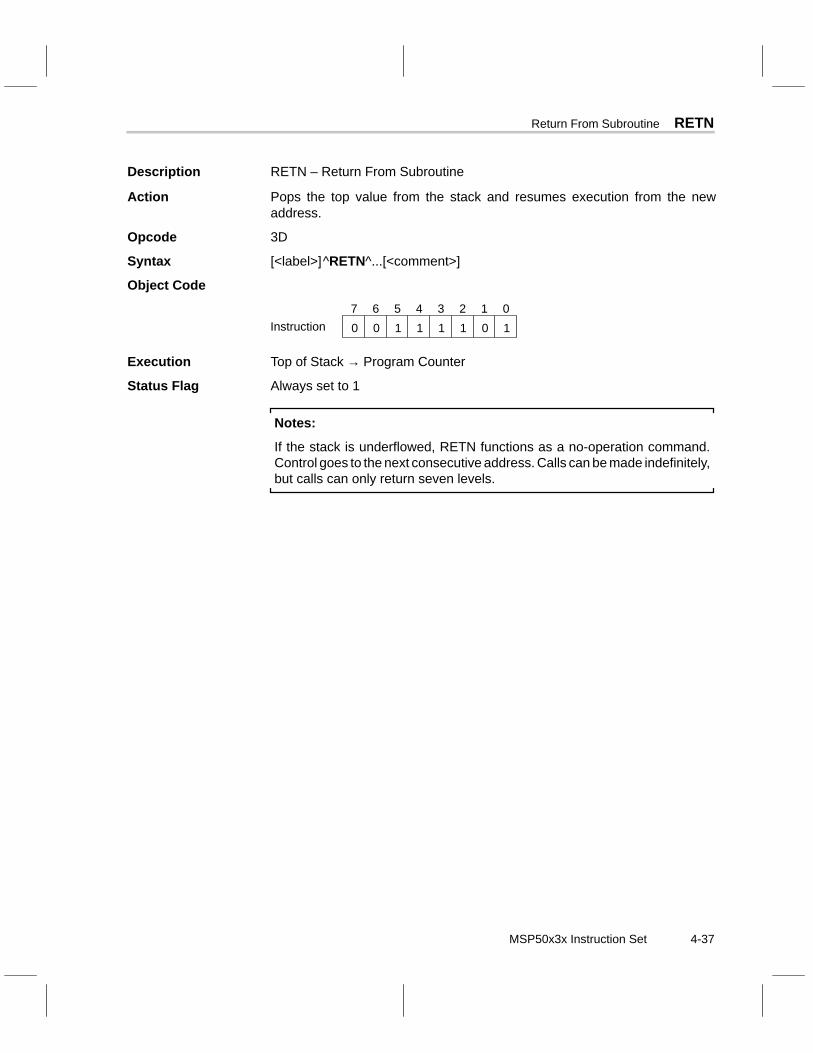
Return From Subroutine RETN
4-37 MSP50x3x Instruction Set
Description RETN – Return From Subroutine
Action Pops the top value from the stack and resumes execution from the newaddress.
Opcode 3D
Syntax [<label>]^RETN^...[<comment>]
Object Code
34567 2 1 0
11100 1 0 1Instruction
Execution Top of Stack → Program Counter
Status Flag Always set to 1
Notes:
If the stack is underflowed, RETN functions as a no-operation command.Control goes to the next consecutive address. Calls can be made indefinitely,but calls can only return seven levels.
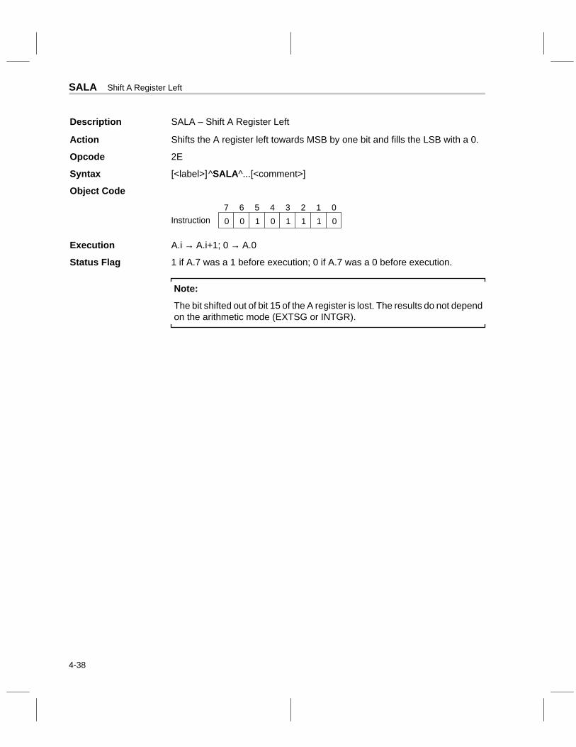
SALA Shift A Register Left
4-38
Description SALA – Shift A Register Left
Action Shifts the A register left towards MSB by one bit and fills the LSB with a 0.
Opcode 2E
Syntax [<label>]^SALA^...[<comment>]
Object Code
34567 2 1 0
10100 1 1 0Instruction
Execution A.i → A.i+1; 0 → A.0
Status Flag 1 if A.7 was a 1 before execution; 0 if A.7 was a 0 before execution.
Note:
The bit shifted out of bit 15 of the A register is lost. The results do not dependon the arithmetic mode (EXTSG or INTGR).
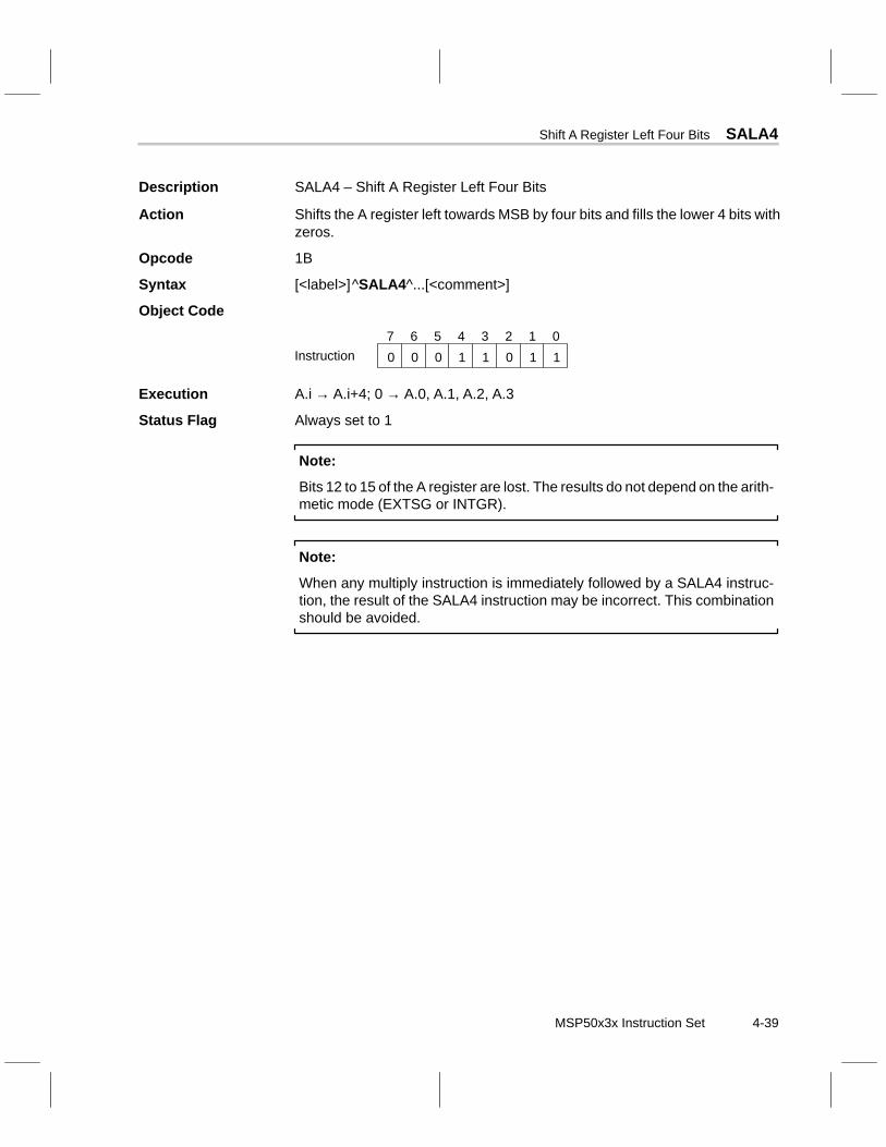
Shift A Register Left Four Bits SALA4
4-39 MSP50x3x Instruction Set
Description SALA4 – Shift A Register Left Four Bits
Action Shifts the A register left towards MSB by four bits and fills the lower 4 bits withzeros.
Opcode 1B
Syntax [<label>]^SALA4^...[<comment>]
Object Code
34567 2 1 0
11000 0 1 1Instruction
Execution A.i → A.i+4; 0 → A.0, A.1, A.2, A.3
Status Flag Always set to 1
Note:
Bits 12 to 15 of the A register are lost. The results do not depend on the arith-metic mode (EXTSG or INTGR).
Note:
When any multiply instruction is immediately followed by a SALA4 instruc-tion, the result of the SALA4 instruction may be incorrect. This combinationshould be avoided.
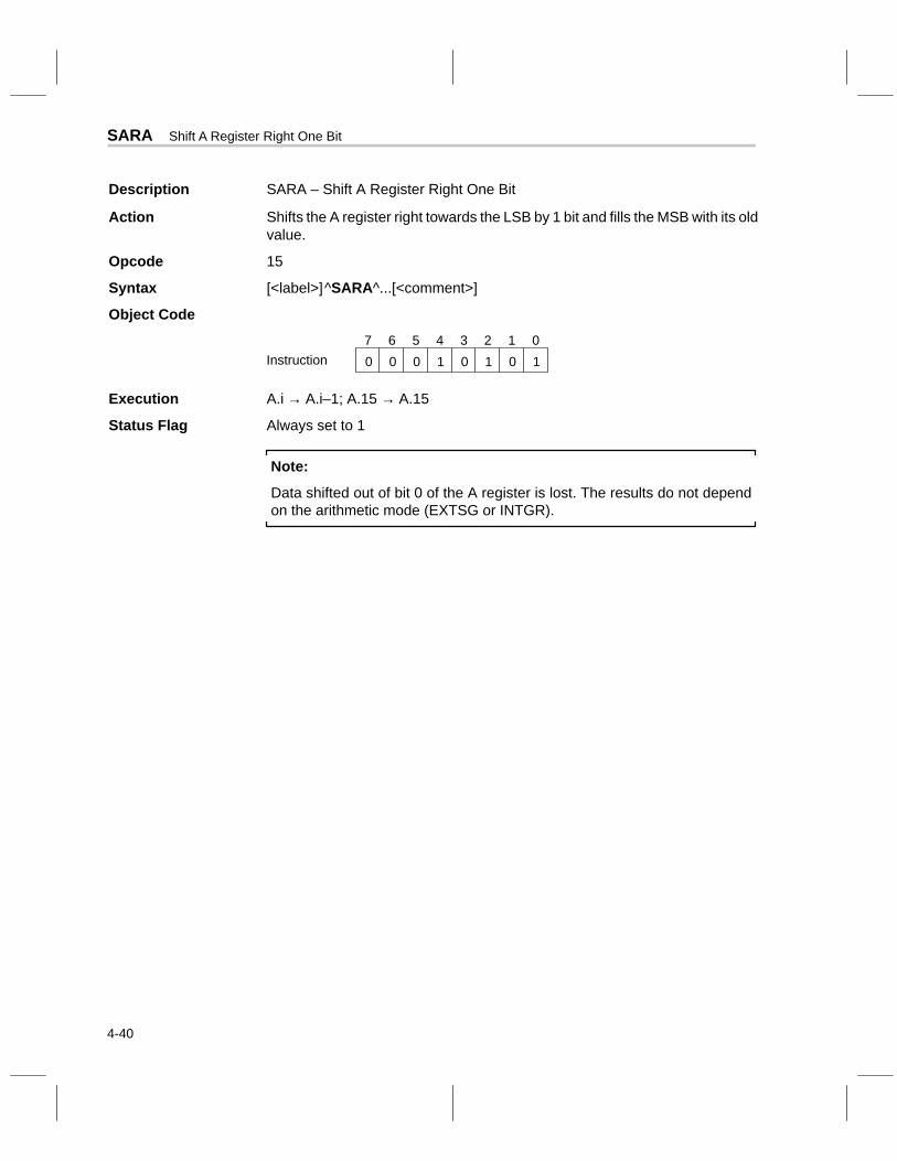
SARA Shift A Register Right One Bit
4-40
Description SARA – Shift A Register Right One Bit
Action Shifts the A register right towards the LSB by 1 bit and fills the MSB with its oldvalue.
Opcode 15
Syntax [<label>]^SARA^...[<comment>]
Object Code
34567 2 1 0
01000 1 0 1Instruction
Execution A.i → A.i–1; A.15 → A.15
Status Flag Always set to 1
Note:
Data shifted out of bit 0 of the A register is lost. The results do not dependon the arithmetic mode (EXTSG or INTGR).
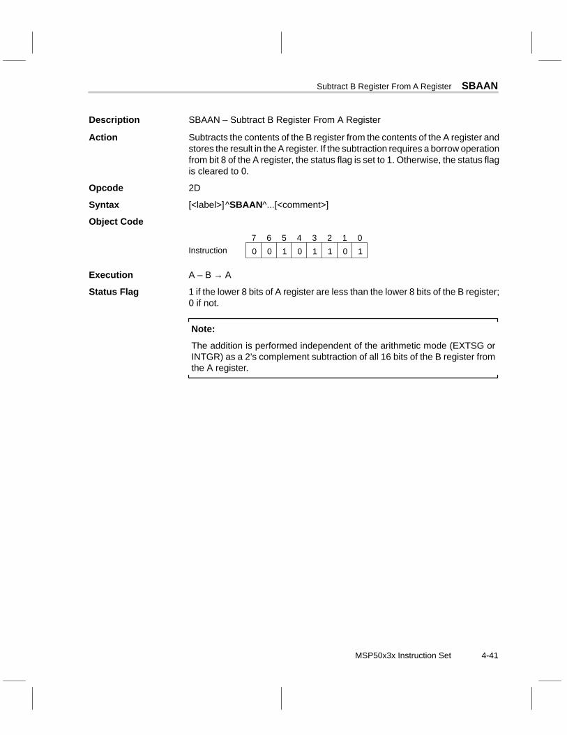
Subtract B Register From A Register SBAAN
4-41 MSP50x3x Instruction Set
Description SBAAN – Subtract B Register From A Register
Action Subtracts the contents of the B register from the contents of the A register andstores the result in the A register. If the subtraction requires a borrow operationfrom bit 8 of the A register, the status flag is set to 1. Otherwise, the status flagis cleared to 0.
Opcode 2D
Syntax [<label>]^SBAAN^...[<comment>]
Object Code
34567 2 1 0
10100 1 0 1Instruction
Execution A – B → A
Status Flag 1 if the lower 8 bits of A register are less than the lower 8 bits of the B register;0 if not.
Note:
The addition is performed independent of the arithmetic mode (EXTSG orINTGR) as a 2’s complement subtraction of all 16 bits of the B register fromthe A register.
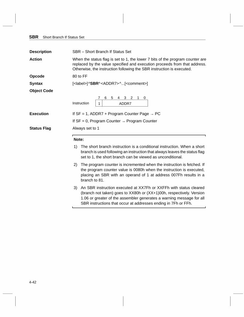
SBR Short Branch If Status Set
4-42
Description SBR – Short Branch If Status Set
Action When the status flag is set to 1, the lower 7 bits of the program counter arereplaced by the value specified and execution proceeds from that address.Otherwise, the instruction following the SBR instruction is executed.
Opcode 80 to FF
Syntax [<label>]^SBR^<ADDR7>^...[<comment>]
Object Code
34567 2 1 0
ADDR71Instruction
Execution If SF = 1, ADDR7 + Program Counter Page → PC
If SF = 0, Program Counter → Program Counter
Status Flag Always set to 1
Note:
1) The short branch instruction is a conditional instruction. When a shortbranch is used following an instruction that always leaves the status flagset to 1, the short branch can be viewed as unconditional.
2) The program counter is incremented when the instruction is fetched. Ifthe program counter value is 0080h when the instruction is executed,placing an SBR with an operand of 1 at address 007Fh results in abranch to 81.
3) An SBR instruction executed at XX7Fh or XXFFh with status cleared(branch not taken) goes to XX80h or (XX+1)00h, respectively. Version1.06 or greater of the assembler generates a warning message for allSBR instructions that occur at addresses ending in 7Fh or FFh.
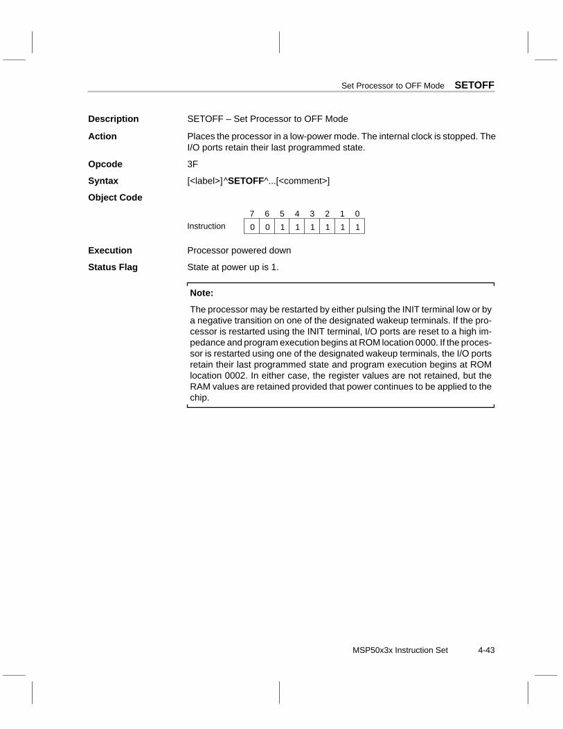
Set Processor to OFF Mode SETOFF
4-43 MSP50x3x Instruction Set
Description SETOFF – Set Processor to OFF Mode
Action Places the processor in a low-power mode. The internal clock is stopped. TheI/O ports retain their last programmed state.
Opcode 3F
Syntax [<label>]^SETOFF^...[<comment>]
Object Code
34567 2 1 0
11100 1 1 1Instruction
Execution Processor powered down
Status Flag State at power up is 1.
Note:
The processor may be restarted by either pulsing the INIT terminal low or bya negative transition on one of the designated wakeup terminals. If the pro-cessor is restarted using the INIT terminal, I/O ports are reset to a high im-pedance and program execution begins at ROM location 0000. If the proces-sor is restarted using one of the designated wakeup terminals, the I/O portsretain their last programmed state and program execution begins at ROMlocation 0002. In either case, the register values are not retained, but theRAM values are retained provided that power continues to be applied to thechip.
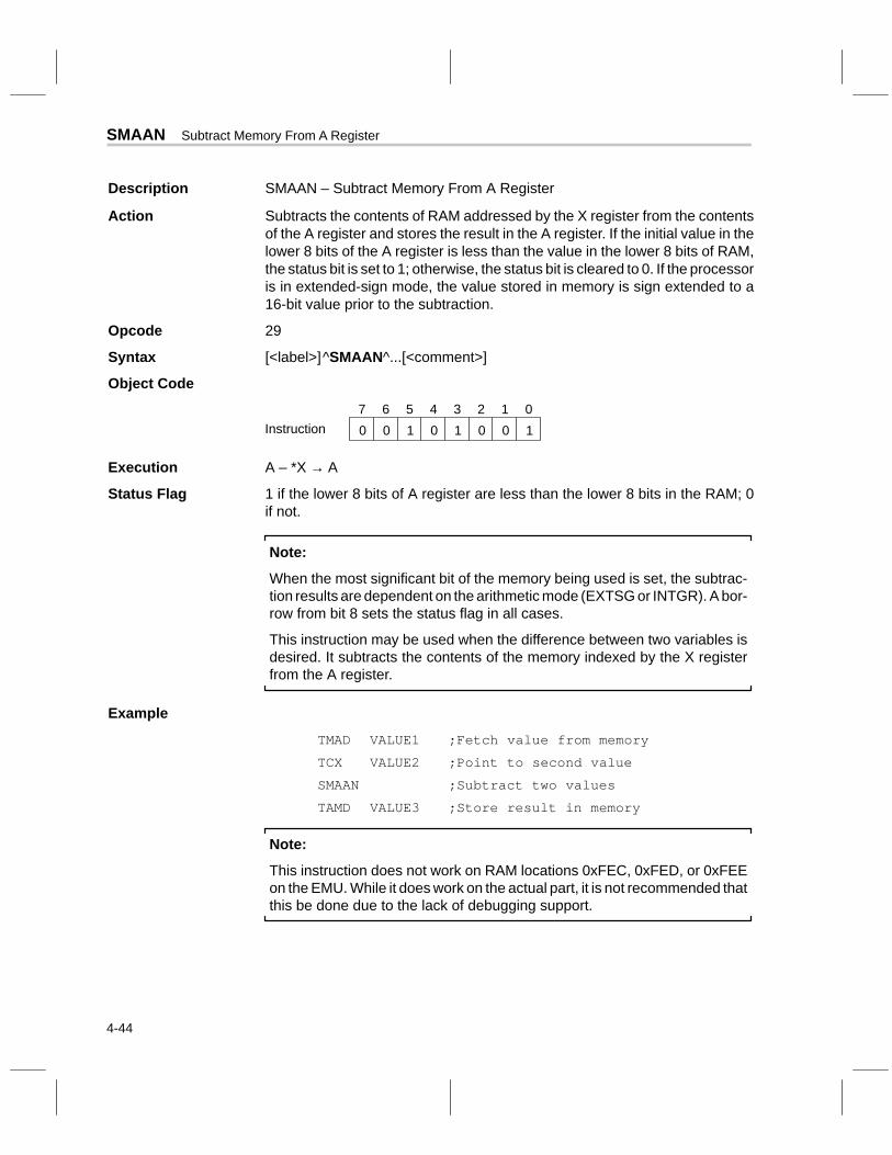
SMAAN Subtract Memory From A Register
4-44
Description SMAAN – Subtract Memory From A Register
Action Subtracts the contents of RAM addressed by the X register from the contentsof the A register and stores the result in the A register. If the initial value in thelower 8 bits of the A register is less than the value in the lower 8 bits of RAM,the status bit is set to 1; otherwise, the status bit is cleared to 0. If the processoris in extended-sign mode, the value stored in memory is sign extended to a16-bit value prior to the subtraction.
Opcode 29
Syntax [<label>]^SMAAN^...[<comment>]
Object Code
34567 2 1 0
10100 0 0 1Instruction
Execution A – *X → A
Status Flag 1 if the lower 8 bits of A register are less than the lower 8 bits in the RAM; 0if not.
Note:
When the most significant bit of the memory being used is set, the subtrac-tion results are dependent on the arithmetic mode (EXTSG or INTGR). A bor-row from bit 8 sets the status flag in all cases.
This instruction may be used when the difference between two variables isdesired. It subtracts the contents of the memory indexed by the X registerfrom the A register.
Example
TMAD VALUE1 ;Fetch value from memory
TCX VALUE2 ;Point to second value
SMAAN ;Subtract two values
TAMD VALUE3 ;Store result in memory
Note:
This instruction does not work on RAM locations 0xFEC, 0xFED, or 0xFEEon the EMU. While it does work on the actual part, it is not recommended thatthis be done due to the lack of debugging support.
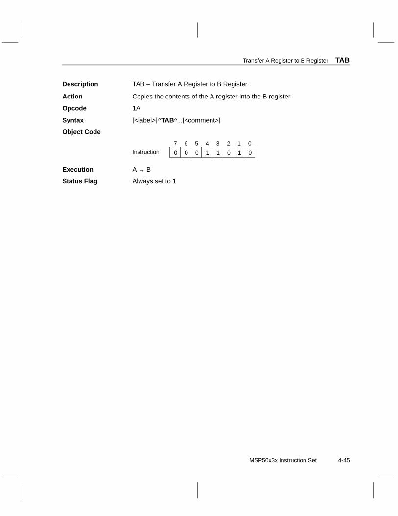
Transfer A Register to B Register TAB
4-45 MSP50x3x Instruction Set
Description TAB – Transfer A Register to B Register
Action Copies the contents of the A register into the B register
Opcode 1A
Syntax [<label>]^TAB^...[<comment>]
Object Code
34567 2 1 0
11000 0 1 0Instruction
Execution A → B
Status Flag Always set to 1
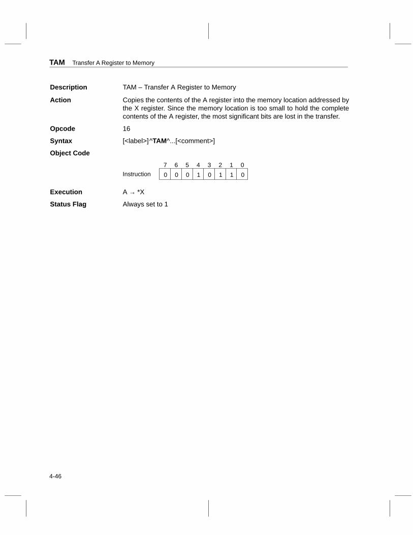
TAM Transfer A Register to Memory
4-46
Description TAM – Transfer A Register to Memory
Action Copies the contents of the A register into the memory location addressed bythe X register. Since the memory location is too small to hold the completecontents of the A register, the most significant bits are lost in the transfer.
Opcode 16
Syntax [<label>]^TAM^...[<comment>]
Object Code
34567 2 1 0
01000 1 1 0Instruction
Execution A → *X
Status Flag Always set to 1
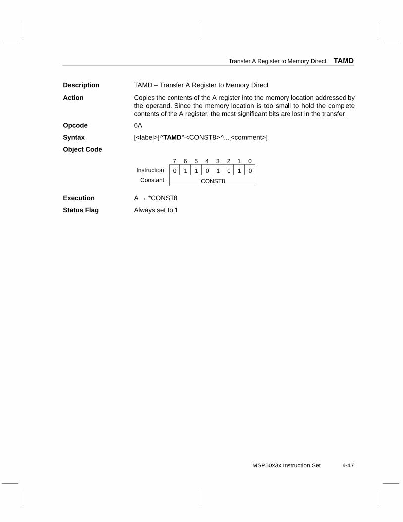
Transfer A Register to Memory Direct TAMD
4-47 MSP50x3x Instruction Set
Description TAMD – Transfer A Register to Memory Direct
Action Copies the contents of the A register into the memory location addressed bythe operand. Since the memory location is too small to hold the completecontents of the A register, the most significant bits are lost in the transfer.
Opcode 6A
Syntax [<label>]^TAMD^<CONST8>^...[<comment>]
Object Code
34567 2 1 0
10110 0 1 0Instruction
CONST8Constant
Execution A → *CONST8
Status Flag Always set to 1
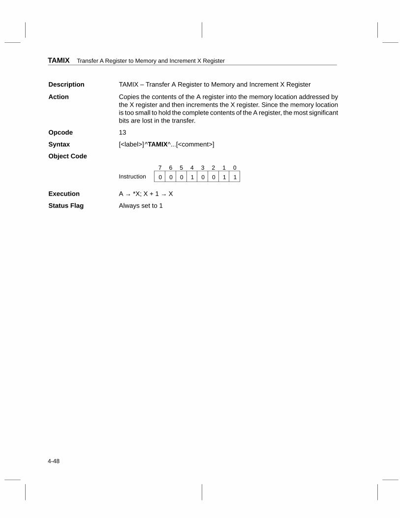
TAMIX Transfer A Register to Memory and Increment X Register
4-48
Description TAMIX – Transfer A Register to Memory and Increment X Register
Action Copies the contents of the A register into the memory location addressed bythe X register and then increments the X register. Since the memory locationis too small to hold the complete contents of the A register, the most significantbits are lost in the transfer.
Opcode 13
Syntax [<label>]^TAMIX^...[<comment>]
Object Code
34567 2 1 0
01000 0 1 1Instruction
Execution A → *X; X + 1 → X
Status Flag Always set to 1
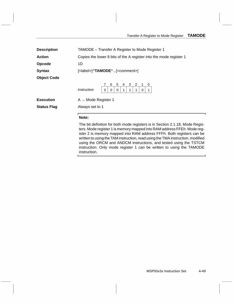
Transfer A Register to Mode Register TAMODE
4-49 MSP50x3x Instruction Set
Description TAMODE – Transfer A Register to Mode Register 1
Action Copies the lower 8 bits of the A register into the mode register 1
Opcode 1D
Syntax [<label>]^TAMODE^...[<comment>]
Object Code
34567 2 1 0
11000 1 0 1Instruction
Execution A → Mode Register 1
Status Flag Always set to 1
Note:
The bit definition for both mode registers is in Section 2.1.18, Mode Regis-ters. Mode register 1 is memory mapped into RAM address FFEh. Mode reg-ister 2 is memory mapped into RAM address FFFh. Both registers can bewritten to using the TAM instruction, read using the TMA instruction, modifiedusing the ORCM and ANDCM instructions, and tested using the TSTCMinstruction. Only mode register 1 can be written to using the TAMODEinstruction.
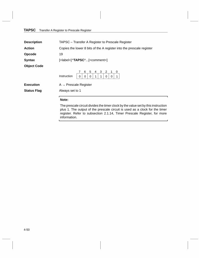
TAPSC Transfer A Register to Prescale Register
4-50
Description TAPSC – Transfer A Register to Prescale Register
Action Copies the lower 8 bits of the A register into the prescale register
Opcode 19
Syntax [<label>]^TAPSC^...[<comment>]
Object Code
34567 2 1 0
11000 0 0 1Instruction
Execution A → Prescale Register
Status Flag Always set to 1
Note:
The prescale circuit divides the timer clock by the value set by this instructionplus 1. The output of the prescale circuit is used as a clock for the timerregister. Refer to subsection 2.1.14, Timer Prescale Register, for moreinformation.
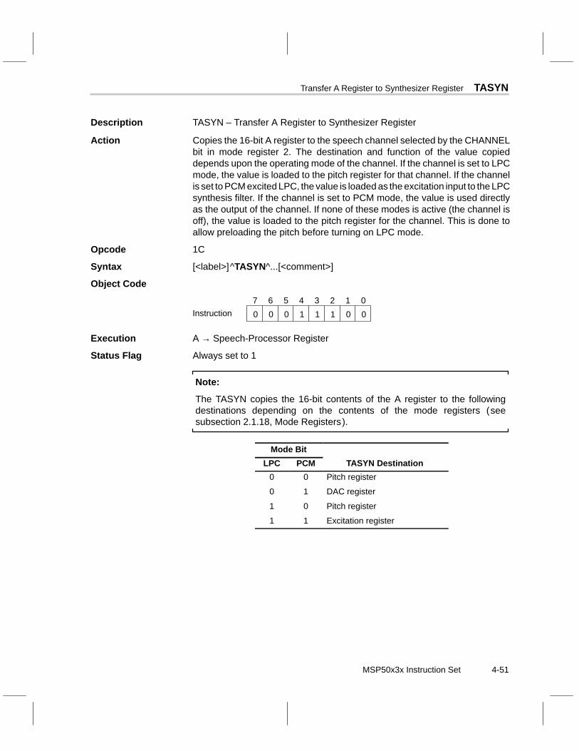
Transfer A Register to Synthesizer Register TASYN
4-51 MSP50x3x Instruction Set
Description TASYN – Transfer A Register to Synthesizer Register
Action Copies the 16-bit A register to the speech channel selected by the CHANNELbit in mode register 2. The destination and function of the value copieddepends upon the operating mode of the channel. If the channel is set to LPCmode, the value is loaded to the pitch register for that channel. If the channelis set to PCM excited LPC, the value is loaded as the excitation input to the LPCsynthesis filter. If the channel is set to PCM mode, the value is used directlyas the output of the channel. If none of these modes is active (the channel isoff), the value is loaded to the pitch register for the channel. This is done toallow preloading the pitch before turning on LPC mode.
Opcode 1C
Syntax [<label>]^TASYN^...[<comment>]
Object Code
34567 2 1 0
11000 1 0 0Instruction
Execution A → Speech-Processor Register
Status Flag Always set to 1
Note:
The TASYN copies the 16-bit contents of the A register to the followingdestinations depending on the contents of the mode registers (seesubsection 2.1.18, Mode Registers ).
Mode Bit
LPC PCM TASYN Destination
0 0 Pitch register
0 1 DAC register
1 0 Pitch register
1 1 Excitation register
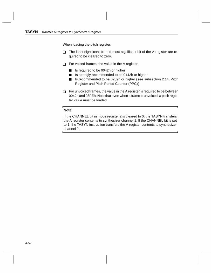
TASYN Transfer A Register to Synthesizer Register
4-52
When loading the pitch register:
The least significant bit and most significant bit of the A register are re-quired to be cleared to zero.
For voiced frames, the value in the A register:
Is required to be 0042h or higher Is strongly recommended to be 0142h or higher Is recommended to be 0202h or higher (see subsection 2.14, Pitch
Register and Pitch Period Counter (PPC) )
For unvoiced frames, the value in the A register is required to be between0042h and 03FEh. Note that even when a frame is unvoiced, a pitch regis-ter value must be loaded.
Note:
If the CHANNEL bit in mode register 2 is cleared to 0, the TASYN transfersthe A register contents to synthesizer channel 1. If the CHANNEL bit is setto 1, the TASYN instruction transfers the A register contents to synthesizerchannel 2.
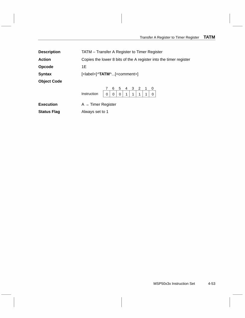
Transfer A Register to Timer Register TATM
4-53 MSP50x3x Instruction Set
Description TATM – Transfer A Register to Timer Register
Action Copies the lower 8 bits of the A register into the timer register
Opcode 1E
Syntax [<label>]^TATM^...[<comment>]
Object Code
34567 2 1 0
11000 1 1 0Instruction
Execution A → Timer Register
Status Flag Always set to 1
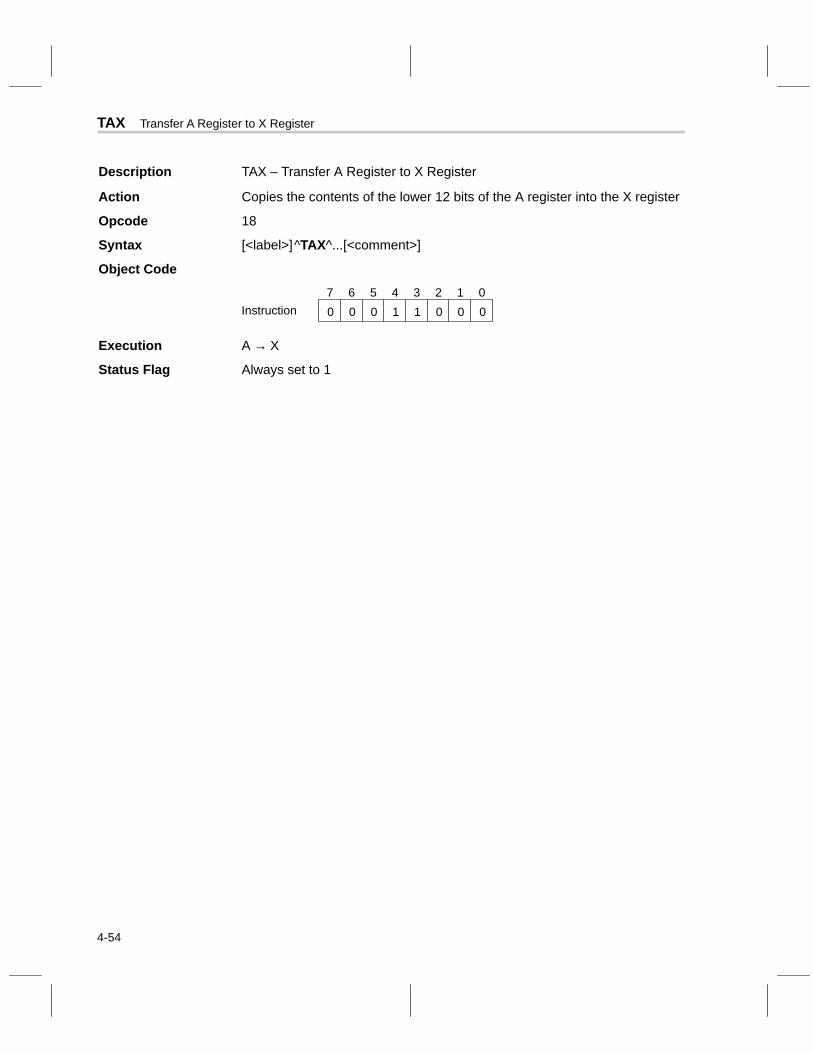
TAX Transfer A Register to X Register
4-54
Description TAX – Transfer A Register to X Register
Action Copies the contents of the lower 12 bits of the A register into the X register
Opcode 18
Syntax [<label>]^TAX^...[<comment>]
Object Code
34567 2 1 0
11000 0 0 0Instruction
Execution A → X
Status Flag Always set to 1
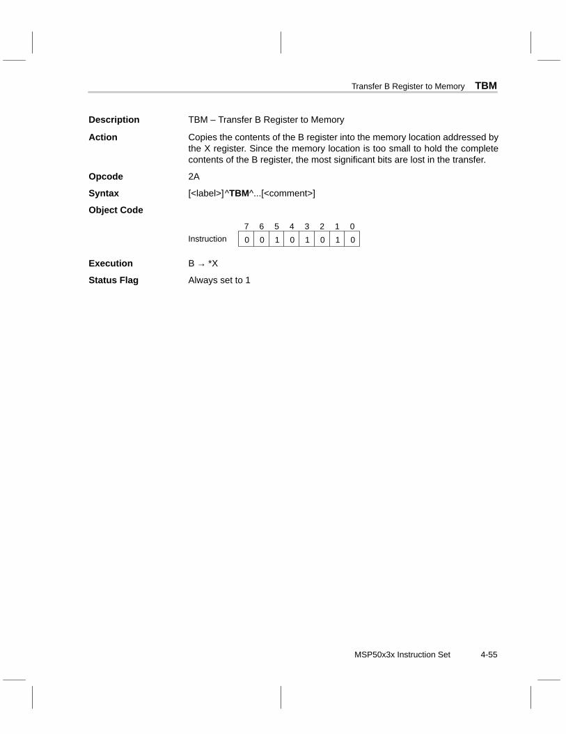
Transfer B Register to Memory TBM
4-55 MSP50x3x Instruction Set
Description TBM – Transfer B Register to Memory
Action Copies the contents of the B register into the memory location addressed bythe X register. Since the memory location is too small to hold the completecontents of the B register, the most significant bits are lost in the transfer.
Opcode 2A
Syntax [<label>]^TBM^...[<comment>]
Object Code
34567 2 1 0
10100 0 1 0Instruction
Execution B → *X
Status Flag Always set to 1
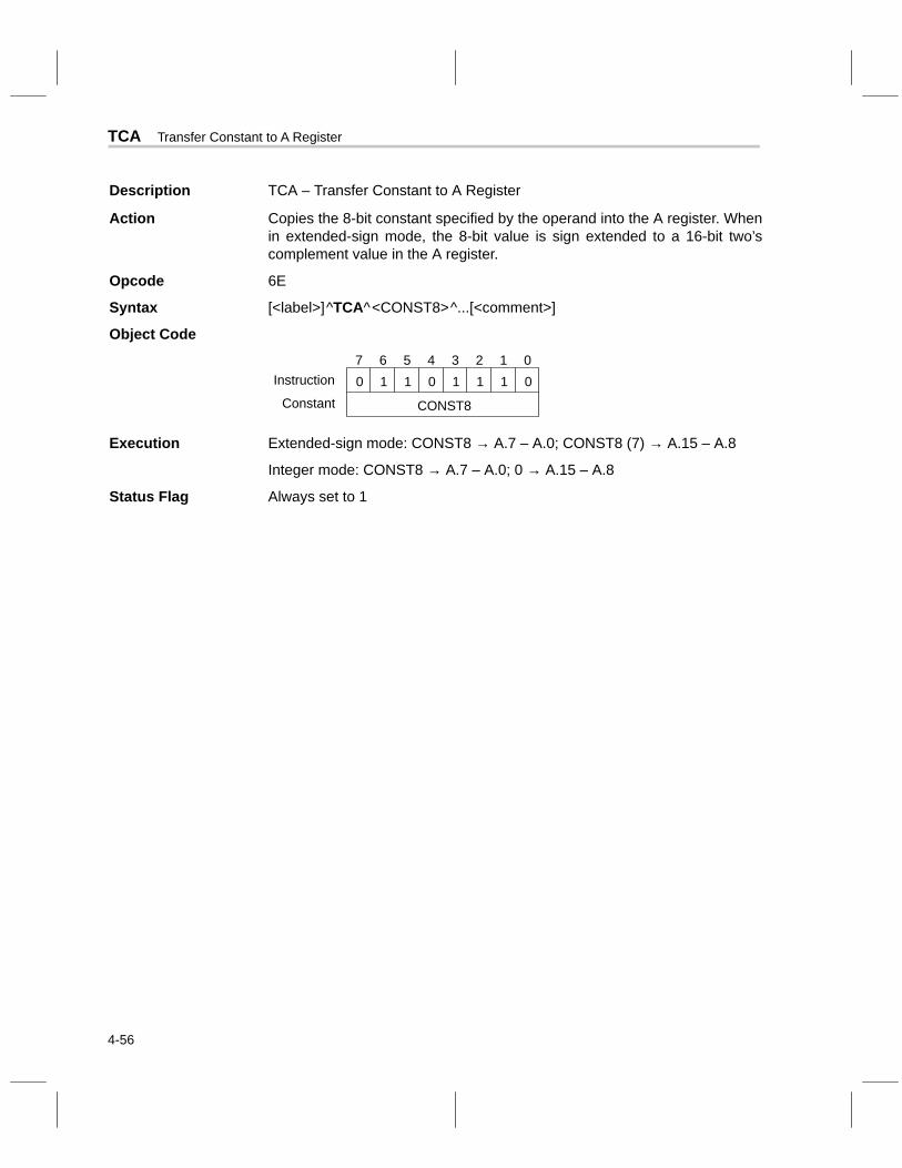
TCA Transfer Constant to A Register
4-56
Description TCA – Transfer Constant to A Register
Action Copies the 8-bit constant specified by the operand into the A register. Whenin extended-sign mode, the 8-bit value is sign extended to a 16-bit two’scomplement value in the A register.
Opcode 6E
Syntax [<label>]^TCA^<CONST8>^...[<comment>]
Object Code
34567 2 1 0
10110 1 1 0Instruction
CONST8Constant
Execution Extended-sign mode: CONST8 → A.7 – A.0; CONST8 (7) → A.15 – A.8
Integer mode: CONST8 → A.7 – A.0; 0 → A.15 – A.8
Status Flag Always set to 1
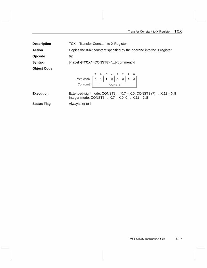
Transfer Constant to X Register TCX
4-57 MSP50x3x Instruction Set
Description TCX – Transfer Constant to X Register
Action Copies the 8-bit constant specified by the operand into the X register
Opcode 62
Syntax [<label>]^TCX^<CONST8>^...[<comment>]
Object Code
34567 2 1 0
00110 0 1 0Instruction
CONST8Constant
Execution Extended-sign mode: CONST8 → X.7 – X.0; CONST8 (7) → X.11 – X.8Integer mode: CONST8 → X.7 – X.0; 0 → X.11 – X.8
Status Flag Always set to 1
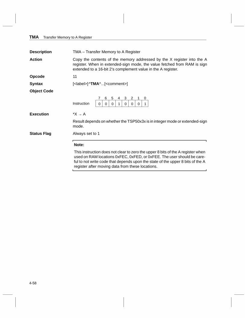
TMA Transfer Memory to A Register
4-58
Description TMA – Transfer Memory to A Register
Action Copy the contents of the memory addressed by the X register into the Aregister. When in extended-sign mode, the value fetched from RAM is signextended to a 16-bit 2’s complement value in the A register.
Opcode 11
Syntax [<label>]^TMA^...[<comment>]
Object Code
34567 2 1 0
01000 0 0 1Instruction
Execution *X → A
Result depends on whether the TSP50x3x is in integer mode or extended-signmode.
Status Flag Always set to 1
Note:
This instruction does not clear to zero the upper 8 bits of the A register whenused on RAM locations 0xFEC, 0xFED, or 0xFEE. The user should be care-ful to not write code that depends upon the state of the upper 8 bits of the Aregister after moving data from these locations.
Transfer Memory to A Register Direct TMAD
4-59 MSP50x3x Instruction Set
Description TMAD – Transfer Memory to A Register Direct
Action Copies the contents of the memory addressed by the operand into the Aregister. When in extended-sign mode, the value fetched from memory is signextended to a 16-bit two’s complement value in the A register.
Opcode 69
Syntax [<label>]^TMAD^<CONST8>^...[<comment>]
Object Code
34567 2 1 0
10110 0 0 1Instruction
CONST8Constant
Execution If 8-bit RAM location then *CONST8 → A
If 12-bit RAM location: (*CONST12)→ (A)
The result depends on whether the MSP50C3x is in integer mode orextended-sign mode.
Status Flag Always set to 1
TMAIX Transfer Memory to A Register and Increment X Register
4-60
Description TMAIX – Transfer Memory to A Register and Increment X Register
Action Copies the contents of the memory location addressed by the X register intothe A register and then increments the X register. When the processor is inextended-sign mode, the value fetched from RAM is sign extended to a 16-bittwo’s complement in the A register.
Opcode 14
Syntax [<label>]^TMAIX^...[<comment>]
Object Code
34567 2 1 0
01000 1 0 0Instruction
Execution *X → A
The result depends on whether the MSP50x3x is in integer mode orextended-sign mode
Status Flag Always set to 1
Note:
This instruction does not clear to zero the upper 8 bits of the A register whenused on RAM locations 0xFEC, 0xFED, 0xFEE, or 0xFEF. The user shouldbe careful to not write code that depends upon the state of the upper 8 bitsof the A register after moving data from these locations.
Transfer Memory Directly to X Register TMXD
4-61 MSP50x3x Instruction Set
Description TMXD – Transfer Memory Directly to X Register
Action Copies the contents of memory addressed by the operand into the X register
Opcode 6F
Syntax [<label>]^TMXD^<CONST8>^...[<comment>]
Object Code
34567 2 1 0
10110 1 1 1Instruction
CONST8Constant
Execution If 8-bit RAM location: *CONST8 → XIf 12-bit RAM location: *CONST12 → X
The result depends on whether the MSP50C3x is in integer mode orextended-sign mode.
Status Flag Always set to 1
TRNDA Transfer Random Number into A Register
4-62
Description TRNDA – Transfer Random Number into A Register
Action Copies an 8-bit random number into the A register. Extended-sign mode doesnot affect the operation of this instruction. The value is not sign extended.
Opcode 2B
Syntax [<label>]^TRNDA^...[<comment>]
Object Code
34567 2 1 0
10100 0 1 1Instruction
Execution Random Number → A
Status Flag Always set to 1
Notes:
1) The random number register generates a pseudorandom count with32,767 states. The algorithm is summarized in the following paragraph.
2) At power up, the random number is initialized to 0. At every subsequentinstruction cycle, the register is left shifted once, and bit 0 is set to theexclusive NOR of bits 13 and 14. The transfer to the A register in re-sponse to TRNDA is done prior to this operation.
3) The value is initialized to zero by the INIT terminal going low. It is not ini-tialized by the SETOFF instruction and subsequent wakeup operation.
Test Constant With A Register TSTCA
4-63 MSP50x3x Instruction Set
Description TSTCA – Test Constant With A Register
Action Compares the constant specified by the operand and the contents of the Aregister. If any bit in the operand is high with the corresponding bit in the Aregister low, the status flag is cleared to 0. Otherwise, the status flag is set to1.
Opcode 67
Syntax [<label>]^TSTCA^<CONST8>^...[<comment>]
Object Code
34567 2 1 0
00110 1 1 1Instruction
CONST8Constant
Execution (A && CONST8 == CONST8) → SF
Status Flag Conditionally set to 1 if every bit that is set to 1 in the operand has acorresponding bit set to 1 in the A register; otherwise it is cleared to 0. If theoperand is 0, then the status flag is set to 1.
Note:
This instruction logically performs an AND operation the value stored in theA register with the value of the 8-bit constant and sets the status flag if theresult is equal to the 8-bit constant. The value in the A register does notchange.
Note:
This instruction does not work on RAM locations 0xFEC, 0xFED, or 0xFEEon the EVM. While it does work on the actual part, it is not recommended dueto the lack of debugging support.
TSTCM Test Constant With Memory
4-64
Description TSTCM – Test Constant With Memory
Action Compares the constant specified by the operand and the contents of thememory location addressed by the X register. If any bit in the operand is highwith the corresponding bit in the memory location low, the status flag is clearedto zero. Otherwise, the status flag is set to 1.
Opcode 66
Syntax [<label>]^TSTCM^<CONST8>^...[<comment>]
Object Code
34567 2 1 0
00110 1 1 0Instruction
CONST8Constant
Execution (*X && CONST8 == CONST8) → SF
Status Flag Conditionally set to 1 if every bit that is set in the operand has a correspondingset bit in the memory addressed by the X register; otherwise it is cleared to 0.If the operand is 0, then the status flag is set to 1.
Note:
This instruction logically ANDs the value stored in the RAM location pointedto by the X register with the value of the 8-bit constant and sets the statusflag if the result is equal to the 8-bit constant. The value in memory is notaffected.
Note:
This instruction does not work on RAM locations 0xFEC, 0xFED, or 0xFEEon the EVM. While it does work on the actual part, it is not recommended thatthis be done due to the lack of debugging support.
Transfer Timer Register to A Register TTMA
4-65 MSP50x3x Instruction Set
Description TTMA – Transfer Timer Register to A Register
Action Copies the contents of the timer register into the A register. When inextended-sign mode, the value fetched from the timer register is sign extendedto a 16-bit 2’s complement number in the A register.
Opcode 17
Syntax [<label>]^TTMA^...[<comment>]
Object Code
34567 2 1 0
01000 1 1 1Instruction
Execution Extended-sign mode:Timer Register → A.7 – A.0;Timer Register7 → A.15 – A.8
Integer mode: Timer Register → A.7 – A.0; 0 → A.15 – A.8
Status Flag Always set to 1
TXA Transfer X Register to A Register
4-66
Description TXA – Transfer X Register to A Register
Action Copies the contents of the X register into the A register. When in extended-signmode, the value transferred from the X register is sign extended into a 16-bittwo’s complement number in the A register.
Opcode 10
Syntax [<label>]^TXA^...[<comment>]
Object Code
34567 2 1 0
01000 0 0 0Instruction
Execution extended-sign mode: X → A.11 – A.0; X.11 → A.15 – A.12
integer mode: X → A.11 – A.0; 0 → A.15 – A.12
Status Flag Always set to 1
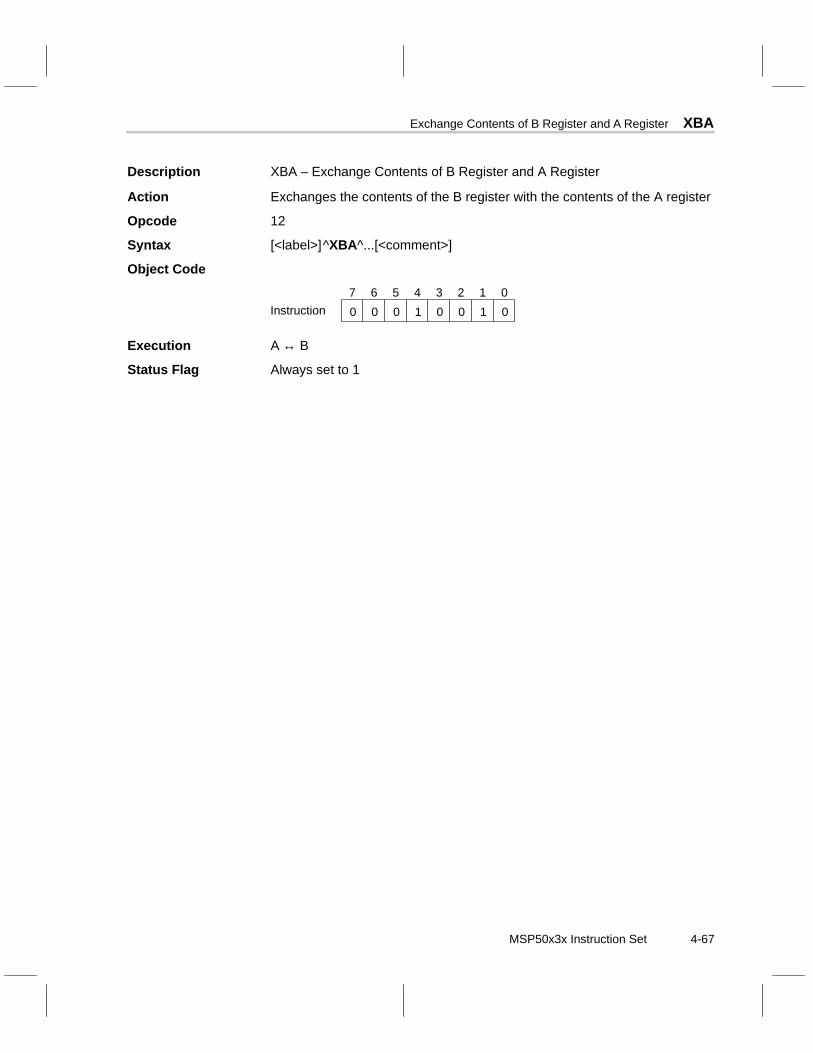
Exchange Contents of B Register and A Register XBA
4-67 MSP50x3x Instruction Set
Description XBA – Exchange Contents of B Register and A Register
Action Exchanges the contents of the B register with the contents of the A register
Opcode 12
Syntax [<label>]^XBA^...[<comment>]
Object Code
34567 2 1 0
01000 0 1 0Instruction
Execution A ↔ B
Status Flag Always set to 1
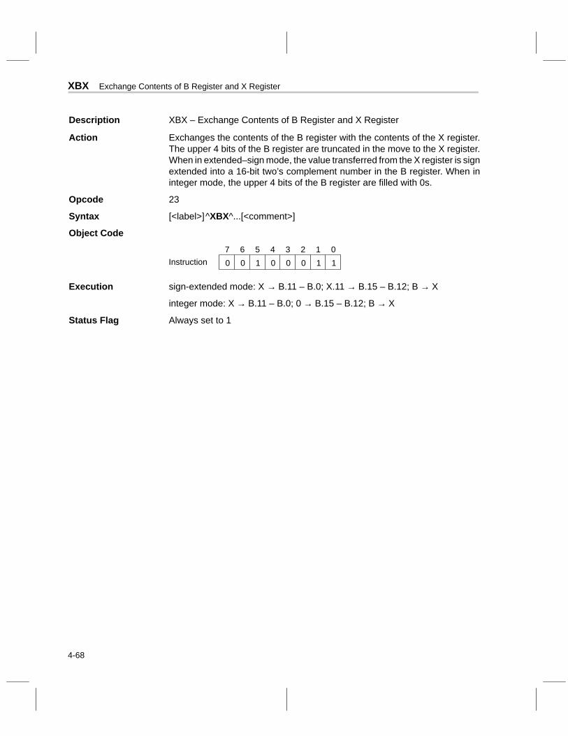
XBX Exchange Contents of B Register and X Register
4-68
Description XBX – Exchange Contents of B Register and X Register
Action Exchanges the contents of the B register with the contents of the X register.The upper 4 bits of the B register are truncated in the move to the X register.When in extended–sign mode, the value transferred from the X register is signextended into a 16-bit two’s complement number in the B register. When ininteger mode, the upper 4 bits of the B register are filled with 0s.
Opcode 23
Syntax [<label>]^XBX^...[<comment>]
Object Code
34567 2 1 0
00100 0 1 1Instruction
Execution sign-extended mode: X → B.11 – B.0; X.11 → B.15 – B.12; B → X
integer mode: X → B.11 – B.0; 0 → B.15 – B.12; B → X
Status Flag Always set to 1
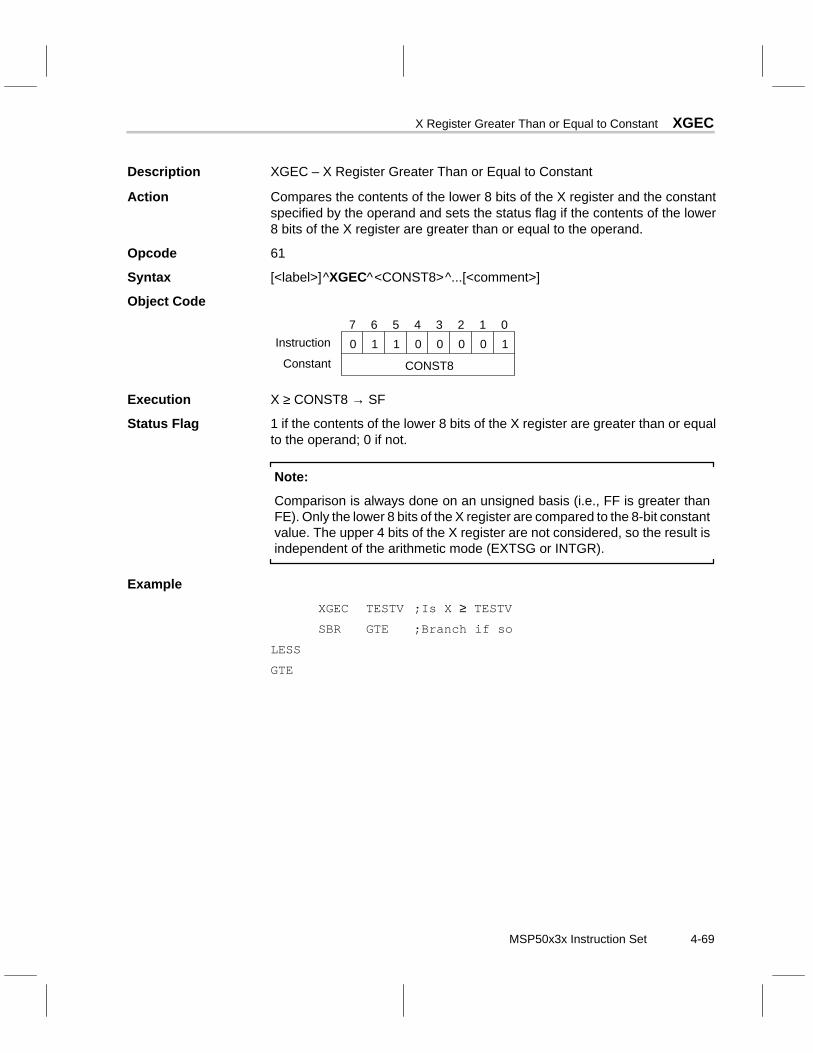
X Register Greater Than or Equal to Constant XGEC
4-69 MSP50x3x Instruction Set
Description XGEC – X Register Greater Than or Equal to Constant
Action Compares the contents of the lower 8 bits of the X register and the constantspecified by the operand and sets the status flag if the contents of the lower8 bits of the X register are greater than or equal to the operand.
Opcode 61
Syntax [<label>]^XGEC^<CONST8>^...[<comment>]
Object Code
34567 2 1 0
00110 0 0 1Instruction
CONST8Constant
Execution X ≥ CONST8 → SF
Status Flag 1 if the contents of the lower 8 bits of the X register are greater than or equalto the operand; 0 if not.
Note:
Comparison is always done on an unsigned basis (i.e., FF is greater thanFE). Only the lower 8 bits of the X register are compared to the 8-bit constantvalue. The upper 4 bits of the X register are not considered, so the result isindependent of the arithmetic mode (EXTSG or INTGR).
Example
XGEC TESTV ;Is X ≥ TESTVSBR GTE ;Branch if so
LESS
GTE

4-70
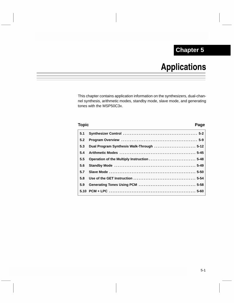
5-1
Applications
This chapter contains application information on the synthesizers, dual-chan-nel synthesis, arithmetic modes, standby mode, slave mode, and generatingtones with the MSP50C3x.
Topic Page
5.1 Synthesizer Control 5-2. . . . . . . . . . . . . . . . . . . . . . . . . . . . . . . . . . . . . . . . . . .
5.2 Program Overview 5-9. . . . . . . . . . . . . . . . . . . . . . . . . . . . . . . . . . . . . . . . . . . .
5.3 Dual Program Synthesis Walk-Through 5-12. . . . . . . . . . . . . . . . . . . . . . . .
5.4 Arithmetic Modes 5-45. . . . . . . . . . . . . . . . . . . . . . . . . . . . . . . . . . . . . . . . . . . .
5.5 Operation of the Multiply Instruction 5-48. . . . . . . . . . . . . . . . . . . . . . . . . . .
5.6 Standby Mode 5-49. . . . . . . . . . . . . . . . . . . . . . . . . . . . . . . . . . . . . . . . . . . . . . .
5.7 Slave Mode 5-50. . . . . . . . . . . . . . . . . . . . . . . . . . . . . . . . . . . . . . . . . . . . . . . . . .
5.8 Use of the GET Instruction 5-54. . . . . . . . . . . . . . . . . . . . . . . . . . . . . . . . . . . .
5.9 Generating Tones Using PCM 5-58. . . . . . . . . . . . . . . . . . . . . . . . . . . . . . . . .
5.10 PCM + LPC 5-60. . . . . . . . . . . . . . . . . . . . . . . . . . . . . . . . . . . . . . . . . . . . . . . . . .
Chapter 5
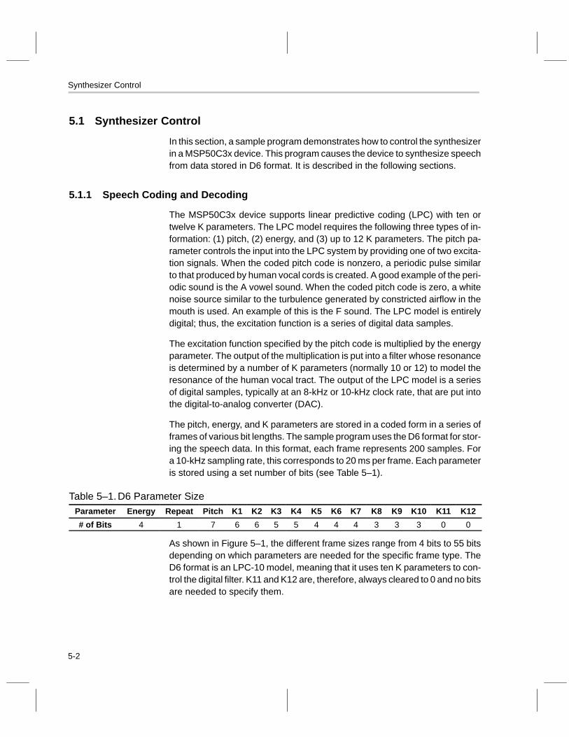
Synthesizer Control
5-2
5.1 Synthesizer Control
In this section, a sample program demonstrates how to control the synthesizerin a MSP50C3x device. This program causes the device to synthesize speechfrom data stored in D6 format. It is described in the following sections.
5.1.1 Speech Coding and Decoding
The MSP50C3x device supports linear predictive coding (LPC) with ten ortwelve K parameters. The LPC model requires the following three types of in-formation: (1) pitch, (2) energy, and (3) up to 12 K parameters. The pitch pa-rameter controls the input into the LPC system by providing one of two excita-tion signals. When the coded pitch code is nonzero, a periodic pulse similarto that produced by human vocal cords is created. A good example of the peri-odic sound is the A vowel sound. When the coded pitch code is zero, a whitenoise source similar to the turbulence generated by constricted airflow in themouth is used. An example of this is the F sound. The LPC model is entirelydigital; thus, the excitation function is a series of digital data samples.
The excitation function specified by the pitch code is multiplied by the energyparameter. The output of the multiplication is put into a filter whose resonanceis determined by a number of K parameters (normally 10 or 12) to model theresonance of the human vocal tract. The output of the LPC model is a seriesof digital samples, typically at an 8-kHz or 10-kHz clock rate, that are put intothe digital-to-analog converter (DAC).
The pitch, energy, and K parameters are stored in a coded form in a series offrames of various bit lengths. The sample program uses the D6 format for stor-ing the speech data. In this format, each frame represents 200 samples. Fora 10-kHz sampling rate, this corresponds to 20 ms per frame. Each parameteris stored using a set number of bits (see Table 5–1).
Table 5–1.D6 Parameter SizeParameter Energy Repeat Pitch K1 K2 K3 K4 K5 K6 K7 K8 K9 K10 K11 K12
# of Bits 4 1 7 6 6 5 5 4 4 4 3 3 3 0 0
As shown in Figure 5–1, the different frame sizes range from 4 bits to 55 bitsdepending on which parameters are needed for the specific frame type. TheD6 format is an LPC-10 model, meaning that it uses ten K parameters to con-trol the digital filter. K11 and K12 are, therefore, always cleared to 0 and no bitsare needed to specify them.
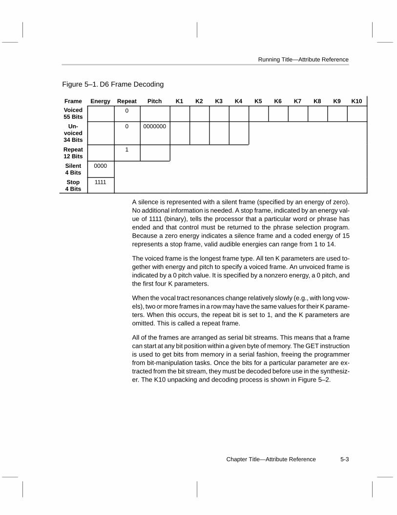
Running Title—Attribute Reference
5-3 Chapter Title—Attribute Reference
Figure 5–1. D6 Frame Decoding
Frame Energy Repeat Pitch K1 K2 K3 K4 K5 K6 K7 K8 K9 K10
Voiced55 Bits
0
Un-voiced34 Bits
0 0000000
Repeat12 Bits
1
Silent4 Bits
0000
Stop4 Bits
1111
A silence is represented with a silent frame (specified by an energy of zero).No additional information is needed. A stop frame, indicated by an energy val-ue of 1111 (binary), tells the processor that a particular word or phrase hasended and that control must be returned to the phrase selection program.Because a zero energy indicates a silence frame and a coded energy of 15represents a stop frame, valid audible energies can range from 1 to 14.
The voiced frame is the longest frame type. All ten K parameters are used to-gether with energy and pitch to specify a voiced frame. An unvoiced frame isindicated by a 0 pitch value. It is specified by a nonzero energy, a 0 pitch, andthe first four K parameters.
When the vocal tract resonances change relatively slowly (e.g., with long vow-els), two or more frames in a row may have the same values for their K parame-ters. When this occurs, the repeat bit is set to 1, and the K parameters areomitted. This is called a repeat frame.
All of the frames are arranged as serial bit streams. This means that a framecan start at any bit position within a given byte of memory. The GET instructionis used to get bits from memory in a serial fashion, freeing the programmerfrom bit-manipulation tasks. Once the bits for a particular parameter are ex-tracted from the bit stream, they must be decoded before use in the synthesiz-er. The K10 unpacking and decoding process is shown in Figure 5–2.

Synthesizer Control
5-4
Figure 5–2. Speech Parameter Unpacking and Decoding
000
K5 K6 K7 K8 K9 K10 E R Pitch K1 K2
Current Frame Next Frame
0101 1110 1110 001 010 100 1101 0 0101110 010110 110100Coded Speech
(Binary)
Unpacked K10 (Binary)
K10 Coding Table
K10 Coded Values (Binary)
K10 Decoded Values (Hex)
Synthesizer RAM
100
001 010 011 100 101 110 111
C3 E6 F3 FD 06 11 1E 43
06K10
To decode speech, the processor must do the following three things: (1) deter-mine the frame type, (2) unpack each parameter, and (3) using a table lookup,decode each parameter. The specific details of these operations are given inSection 5.2, Program Overview,. The processor is also required to decide ifeach frame should be interpolated. Interpolation is used to smooth out thetransitions between frames.
Most of the time, speech changes smoothly. If 20-ms frames are used withoutinterpolation, changes occur abruptly and the speech sounds rough. TheMSP50C3x devices require the program to interpolate the parameters. Whenspeech changes quickly, as in the case of a transition between a voiced frameand an unvoiced frame, interpolation should not be performed. Therefore, thesample program disables interpolation at voicing transition.
5.1.2 RAM Usage
In the following discussion, all the addresses are given in hexadecimal nota-tion.
The sample program uses 108 RAM locations. During synthesis, use of the12-bit RAM locations 00h through 1Fh are fixed by the architecture of theMSP50C3x. As shown in Table 5–2, these locations are assumed by the syn-thesizer to contain the working values of the LPC speech parameters. Thenames given in parentheses are the variable names used in the sample pro-gram. When synthesis is disabled, these locations can be used at the program-mer’s discretion. Also, if only channel 1 is being used, the locations for channel2 can be used elsewhere.
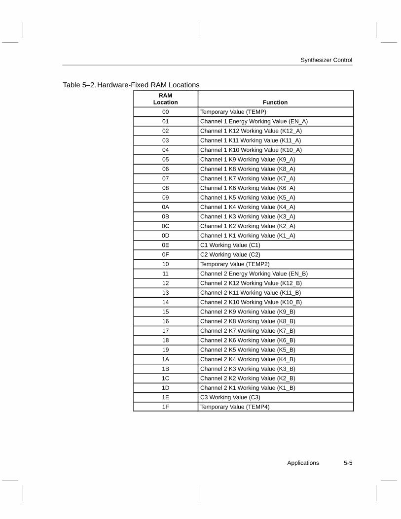
Synthesizer Control
5-5 Applications
Table 5–2.Hardware-Fixed RAM LocationsRAM
Location Function
00 Temporary Value (TEMP)
01 Channel 1 Energy Working Value (EN_A)
02 Channel 1 K12 Working Value (K12_A)
03 Channel 1 K11 Working Value (K11_A)
04 Channel 1 K10 Working Value (K10_A)
05 Channel 1 K9 Working Value (K9_A)
06 Channel 1 K8 Working Value (K8_A)
07 Channel 1 K7 Working Value (K7_A)
08 Channel 1 K6 Working Value (K6_A)
09 Channel 1 K5 Working Value (K5_A)
0A Channel 1 K4 Working Value (K4_A)
0B Channel 1 K3 Working Value (K3_A)
0C Channel 1 K2 Working Value (K2_A)
0D Channel 1 K1 Working Value (K1_A)
0E C1 Working Value (C1)
0F C2 Working Value (C2)
10 Temporary Value (TEMP2)
11 Channel 2 Energy Working Value (EN_B)
12 Channel 2 K12 Working Value (K12_B)
13 Channel 2 K11 Working Value (K11_B)
14 Channel 2 K10 Working Value (K10_B)
15 Channel 2 K9 Working Value (K9_B)
16 Channel 2 K8 Working Value (K8_B)
17 Channel 2 K7 Working Value (K7_B)
18 Channel 2 K6 Working Value (K6_B)
19 Channel 2 K5 Working Value (K5_B)
1A Channel 2 K4 Working Value (K4_B)
1B Channel 2 K3 Working Value (K3_B)
1C Channel 2 K2 Working Value (K2_B)
1D Channel 2 K1 Working Value (K1_B)
1E C3 Working Value (C3)
1F Temporary Value (TEMP4)
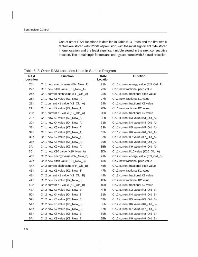
Synthesizer Control
5-6
Use of other RAM locations is detailed in Table 5–3. Pitch and the first two Kfactors are stored with 12 bits of precision, with the most significant byte storedin one location and the least significant nibble stored in the next consecutivelocation. The remaining K factors and energy are stored with 8 bits of precision.
Table 5–3.Other RAM Locations Used in Sample ProgramRAM
LocationFunction RAM
LocationFunction
20h Ch.1 new energy value (EN_New_A) 21h Ch.1 current energy value (EN_Old_A)
22h Ch.1 new pitch value (PH_New_A) 23h Ch.1 new fractional pitch value
24h Ch.1 current pitch value (PH_Old_A) 25h Ch.1 current fractional pitch value
26h Ch.1 new K1 value (K1_New_A) 27h Ch.1 new fractional K1 value
28h Ch.1 current K1 value (K1_Old_A) 29h Ch.1 current fractional K1 value
2Ah Ch.1 new K2 value (K2_New_A) 2Bh Ch.1 new fractional K2 value
2Ch Ch.1 current K2 value (K2_Old_A) 2Dh Ch.1 current fractional K2 value
2Eh Ch.1 new K3 value (K3_New_A) 2Fh Ch.1 current K3 value (K3_Old_A)
30h Ch.1 new K4 value (K4_New_A) 31h Ch.1 current K4 value (K4_Old_A)
32h Ch.1 new K5 value (K5_New_A) 33h Ch.1 current K5 value (K5_Old_A)
34h Ch.1 new K6 value (K6_New_A) 35h Ch.1 current K6 value (K6_Old_A)
36h Ch.1 new K7 value (K7_New_A) 37h Ch.1 current K7 value (K7_Old_A)
38h Ch.1 new K8 value (K8_New_A) 39h Ch.1 current K8 value (K8_Old_A)
3Ah Ch.1 new K9 value (K9_New_A) 3Bh Ch.1 current K9 value (K9_Old_A)
3Ch Ch.1 new K10 value (K10_New_A) 3Dh Ch.1 current K10 value (K10_Old_A)
40h Ch.2 new energy value (EN_New_B) 41h Ch.2 current energy value (EN_Old_B)
42h Ch.2 new pitch value (PH_New_B) 43h Ch.2 new fractional pitch value
44h Ch.2 current pitch value (PH_Old_B) 45h Ch.2 current fractional pitch value
46h Ch.2 new K1 value (K1_New_B) 47h Ch.2 new fractional K1 value
48h Ch.2 current K1 value (K1_Old_B) 49h Ch.2 current fractional K1 value
4Ah Ch.2 new K2 value (K2_New_B) 4Bh Ch.2 new fractional K2 value
4Ch Ch.2 current K2 value (K2_Old_B) 4Dh Ch.2 current fractional K2 value
4Eh Ch.2 new K3 value (K3_New_B) 4Fh Ch.2 current K3 value (K3_Old_B)
50h Ch.2 new K4 value (K4_New_B) 51h Ch.2 current K4 value (K4_Old_B)
52h Ch.2 new K5 value (K5_New_B) 53h Ch.2 current K5 value (K5_Old_B)
54h Ch.2 new K6 value (K6_New_B) 55h Ch.2 current K6 value (K6_Old_B)
56h Ch.2 new K7 value (K7_New_B) 57h Ch.2 current K7 value (K7_Old_B)
58h Ch.2 new K8 value (K8_New_B) 59h Ch.2 current K8 value (K8_Old_B)
5Ah Ch.2 new K9 value (K9_New_B) 5Bh Ch.2 current K9 value (K9_Old_B)
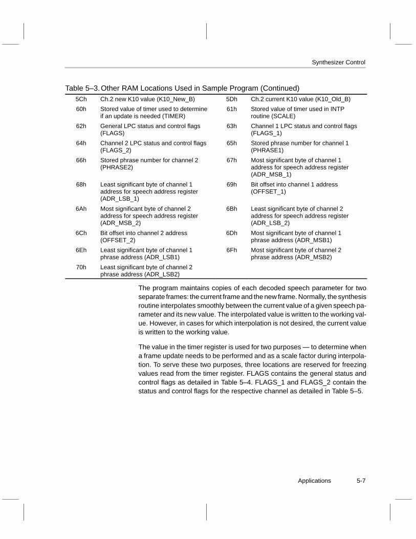
Synthesizer Control
5-7 Applications
Table 5–3.Other RAM Locations Used in Sample Program (Continued)5Ch Ch.2 new K10 value (K10_New_B) 5Dh Ch.2 current K10 value (K10_Old_B)
60h Stored value of timer used to determineif an update is needed (TIMER)
61h Stored value of timer used in INTProutine (SCALE)
62h General LPC status and control flags(FLAGS)
63h Channel 1 LPC status and control flags(FLAGS_1)
64h Channel 2 LPC status and control flags(FLAGS_2)
65h Stored phrase number for channel 1(PHRASE1)
66h Stored phrase number for channel 2(PHRASE2)
67h Most significant byte of channel 1address for speech address register(ADR_MSB_1)
68h Least significant byte of channel 1 address for speech address register(ADR_LSB_1)
69h Bit offset into channel 1 address(OFFSET_1)
6Ah Most significant byte of channel 2 address for speech address register(ADR_MSB_2)
6Bh Least significant byte of channel 2 address for speech address register(ADR_LSB_2)
6Ch Bit offset into channel 2 address (OFFSET_2)
6Dh Most significant byte of channel 1 phrase address (ADR_MSB1)
6Eh Least significant byte of channel 1phrase address (ADR_LSB1)
6Fh Most significant byte of channel 2 phrase address (ADR_MSB2)
70h Least significant byte of channel 2phrase address (ADR_LSB2)
The program maintains copies of each decoded speech parameter for twoseparate frames: the current frame and the new frame. Normally, the synthesisroutine interpolates smoothly between the current value of a given speech pa-rameter and its new value. The interpolated value is written to the working val-ue. However, in cases for which interpolation is not desired, the current valueis written to the working value.
The value in the timer register is used for two purposes — to determine whena frame update needs to be performed and as a scale factor during interpola-tion. To serve these two purposes, three locations are reserved for freezingvalues read from the timer register. FLAGS contains the general status andcontrol flags as detailed in Table 5–4. FLAGS_1 and FLAGS_2 contain thestatus and control flags for the respective channel as detailed in Table 5–5.
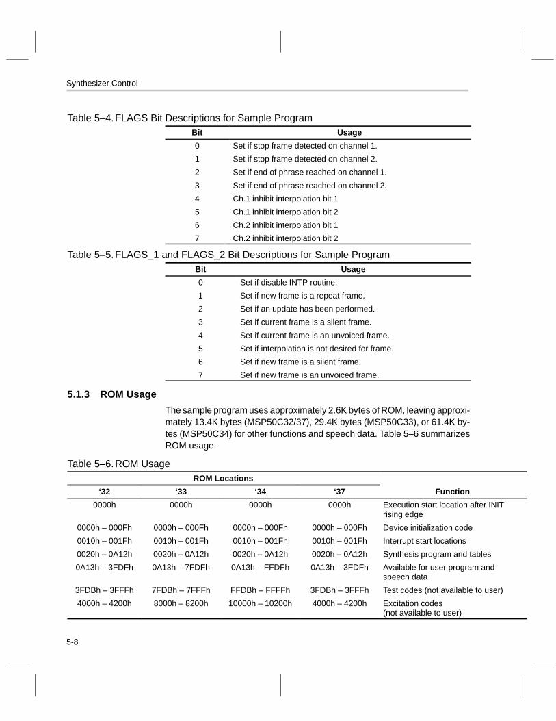
Synthesizer Control
5-8
Table 5–4.FLAGS Bit Descriptions for Sample ProgramBit Usage
0 Set if stop frame detected on channel 1.
1 Set if stop frame detected on channel 2.
2 Set if end of phrase reached on channel 1.
3 Set if end of phrase reached on channel 2.
4 Ch.1 inhibit interpolation bit 1
5 Ch.1 inhibit interpolation bit 2
6 Ch.2 inhibit interpolation bit 1
7 Ch.2 inhibit interpolation bit 2
Table 5–5.FLAGS_1 and FLAGS_2 Bit Descriptions for Sample ProgramBit Usage
0 Set if disable INTP routine.
1 Set if new frame is a repeat frame.
2 Set if an update has been performed.
3 Set if current frame is a silent frame.
4 Set if current frame is an unvoiced frame.
5 Set if interpolation is not desired for frame.
6 Set if new frame is a silent frame.
7 Set if new frame is an unvoiced frame.
5.1.3 ROM Usage
The sample program uses approximately 2.6K bytes of ROM, leaving approxi-mately 13.4K bytes (MSP50C32/37), 29.4K bytes (MSP50C33), or 61.4K by-tes (MSP50C34) for other functions and speech data. Table 5–6 summarizesROM usage.
Table 5–6.ROM UsageROM Locations
‘32 ‘33 ‘34 ‘37 Function
0000h 0000h 0000h 0000h Execution start location after INITrising edge
0000h – 000Fh 0000h – 000Fh 0000h – 000Fh 0000h – 000Fh Device initialization code
0010h – 001Fh 0010h – 001Fh 0010h – 001Fh 0010h – 001Fh Interrupt start locations
0020h – 0A12h 0020h – 0A12h 0020h – 0A12h 0020h – 0A12h Synthesis program and tables
0A13h – 3FDFh 0A13h – 7FDFh 0A13h – FFDFh 0A13h – 3FDFh Available for user program andspeech data
3FDBh – 3FFFh 7FDBh – 7FFFh FFDBh – FFFFh 3FDBh – 3FFFh Test codes (not available to user)
4000h – 4200h 8000h – 8200h 10000h – 10200h 4000h – 4200h Excitation codes(not available to user)
Program Overview
5-9 Applications
5.2 Program Overview
The sample dual synthesis program, parts of which are used in this section forexplanation, is reproduced in its entirety in Appendix C, MSP50C3x SampleDual Synthesis Program. The following is an outline of the program flow:
Initialize processor Initialize speech address register, pitch, C1, and C2 Decode first two frames of speech Start the synthesizer Until the stop frame is reached:
Decode each frame When aninterrupt occurs, recalculate working parameter values
Wait two frames, then stop the synthesizer Return to calling routine
The five main sections of the program are summarized in the following sec-tions.
5.2.1 Initialization
The device state is unknown at device power up. The initialization section ini-tializes the RAM and the mode register to a known state. In the sample pro-gram, this is accomplished by writing zeros to all RAM locations and to themode register.
5.2.2 Phrase Selection
In general, the phrase section contains all application-specific code. In thesample program, this section merely contains repeated calls to the subroutineSPEAK, causing successive utterances to be spoken.
5.2.3 Speech Initialization
The speech initialization section consists of the subroutine SPEAK. It decodesthe numbers contained in the A and B registers for a series of words into theaddresses in ROM. It initializes the TSP50C3x for LPC synthesis on bothchannels and speaks the series of words that comprise the desired sentences.For each word in the sentence, SPEAK enables synthesis and loops until theutterance is complete. It then branches back to speak the next word in the sen-tence. This continues until the sentence is complete.
During each branch of the loop, the value in the timer register is polled. Thenext frame of speech data is read in each time the timer register underflows.
Program Overview
5-10
5.2.4 Interpolation Routine
Once a synthesizer is enabled by SPEAK, it writes a new value to the DACapproximately once every 60 or 90 instruction cycles. The value that is writtenis calculated from the values contained in RAM locations 01h to 0Fh for chan-nel 1 or 11h to 1Fh for channel 2 and the contents of the pitch period counters(PPC1 and PPC2). Loading these locations with the correct values is the re-sponsibility of the program checking the PPC bits (PPC1 and PPC2) and call-ing the appropriate interpolation routine (INTP1 or INTP2). The PPC bits areset hto 1 whenever the PPC decrements below 200h.
When interpolation is not inhibited, INTP performs a linear interpolation be-tween the current value of each speech parameter and its new value using thevalue in the timer register to scale the interpolation. While it is possible to sim-ply load the frame data to the working data, in practice, this results in speechthat sounds rough due to the sharp transition between the different frames. Tominimize this problem, INTP normally performs a linear interpolation betweenthe current and new frames for each of the speech parameters. However, thisis not always appropriate.
There are two cases in which the interpolation is inhibited and the transitionis handled abruptly. When done, INTP simply copies the current values into theworking values.
Transition between voiced and unvoiced frames or between unvoiced andvoiced frames — A different number of K parameters are used in voicedframes than in unvoiced frames, and the K parameters are different. At-tempting to interpolate across the voicing transition results in strangesounds.
An unvoiced frame following a silence — Plosives (e.g., the |Phaa| in theletter |P| are abrupt unvoiced sounds). Trying to interpolate this case re-sults in a gradual ramp up of a plosive, which is incorrect. In the corre-sponding case of a voiced frame following a silence, it is acceptable to in-terpolate.
Program Overview
5-11 Applications
5.2.5 Frame-Update Routine
LPC speech is coded as a series of frames spaced in time. Periodically, thenext frame must be read so that INTP (the interpolation routine) has new datato work with. This is the responsibility of the UPDATE routine. It reads thecoded speech data contained in the next frame, determines what type of frameit is, decodes the speech data contained in the frame, and determines whetheror not interpolation should be performed by INTP.
When a stop frame is encountered, a flag is set that causes the INTP routineto interpolate down to a silence. The synthesizer and the interpolation are bothinhibited by the next pass through the update routine.
Dual Synthesis Program Walk-Through
5-12
5.3 Dual Synthesis Program Walk-Through
The following is a walk-through of a simple MSP50C3x speech dual synthesisprogram. The approach used in this program is not the only possible approach,but it has the advantage of being relatively easy to explain. The complete list-ing of this program can be found in Appendix C, MSP50C3x Sample Dual Syn-thesis Program.
On power up, the processor begins executing code at location 0000h. On wa-keup, the processor begins executing code at location 0002h. This way, theuser can distinguish between a power up and a wakeup by putting differentcode at these locations. To make things simple, the sample program has thesame code at these locations.
0005 ***********************************************************
0006 * Start of program
0007 ***********************************************************
0008 0000 AORG #0000
0009 84 SBR GOGO ;Power up Vector
0010 0001 84 SBR GOGO ;(twice makes unconditional)
0011
0012 0002 84 SBR GOGO ;Wake up vector (same as power up)
0013 0003 84 SBR GOGO ;(twice makes unconditional)
0014
0015 0004 4022 GOGO BR GO ;Branch to start of program
In this sample program, ROM addresses 0006h to 000Fh are not used. ROMaddresses 0010h to 001F contain branches to the interrupt service routines.This section of the ROM address space is dedicated to these service routinesby the MSP50x3x architecture. When an interrupt condition is generated, if theinterrupt is enabled in the mode register, the contents of the program counterare replaced by the address of the appropriate interrupt vector. Normally, theinstruction placed at the interrupt vector address is a branch to the actual rou-tine. Because any branch instruction is conditional upon the value of the statusbit and the value of the status bit is unknown, two short branches to the inter-rupt routine are used instead of a long branch. If the interrupt service routineis not within reach of a short branch, the target of the short branches shouldbe a long branch to the interrupt service routine.
In this sample program, none of the possible eight interrupt conditions areused. The eight unused vectors point to a dummy routine that has no effect.
0017 ***********************************************************
0018 * Interrupt vectors
Dual Synthesis Program Walk-Through
5-13 Applications
0019 ***********************************************************
0020 0010 AORG #0010
0021 A0 SBR INT2_00 ;Timer Underflow, PCM=0, LPC = 0
0022 0011 A0 SBR INT2_00 ;Timer Underflow, PCM=0, LPC = 0
0023 0012 A0 SBR INT2_01 ;Timer Underflow, PCM=0, LPC = 1
0024 0013 A0 SBR INT2_01 ;Timer Underflow, PCM=0, LPC = 1
0025 0014 A0 SBR INT2_10 ;Timer Underflow, PCM=1, LPC = 0
0026 0015 A0 SBR INT2_10 ;Timer Underflow, PCM=1, LPC = 0
0027 0016 A0 SBR INT2_11 ;Timer Underflow, PCM=1, LPC = 1
0028 0017 A0 SBR INT2_11 ;Timer Underflow, PCM=1, LPC = 1
0029 0018 A0 SBR INT1_00 ;Pin (B1) goes low interrupt
0030 0019 A0 SBR INT1_00 ;Pin (B1) goes low interrupt
0031 001A A0 SBR INT1_01 ;Clock interrupt, PCM=0, LPC = 1
0032 001B A0 SBR INT1_01 ;Clock interrupt, PCM=0, LPC = 1
0033 001C A0 SBR INT1_10 ;Clock interrupt, PCM=1, LPC = 0
0034 001D A0 SBR INT1_10 ;Clock interrupt, PCM=1, LPC = 0
0035 001E A0 SBR INT1_11 ;Clock interrupt, PCM=1, LPC = 1
0036 001F A0 SBR INT1_11 ;Clock interrupt, PCM=1, LPC = 1
0037
0038 INT1_10
0039 INT1_01
0040 INT2_10
0041 INT2_00
0042 INT2_01
0043 INT2_11
0044 INT1_00
0045 0020 2F INT1_11 CLA
0046 0021 3E RETI
The following code initializes the processor by clearing the mode registers andthe RAM. Since the first TMAD instruction after power up is not guaranteed tofunction correctly, a TMAD instruction is included in the initialization code. Thisensures that the internal addressing is initialized correctly.
0293 ***********************************************************
0294 * Do program INITs
0295 ***********************************************************
0296 0022 6900 GO TMAD 0
Dual Synthesis Program Walk-Through
5-14
0297
0298 0024 2F CLA ;clear A to zero
0299 0025 20 CLX ;clear X to zero
0300 0026 22 DECXN ;point to location #FFF
0301 0027 16 TAM ;Initialize Mode Register 2
0302 0028 22 DECXN ;point to location #FFE
0303 0029 16 TAM ;Initialize Mode Register 1
0304
0305 002A 20 CLX ;clear X to zero
0306 002B 13 RAM_LOOP TAMIX ;Initialize All RAM to zeros
0307 002C 6180 XGEC MAX_RAM+1 ;all RAM initialized?
0308 002E 4032 BR RAM_EXIT ;yes, exit loop
0309 0030 402B BR RAM_LOOP ;no, continue looping
Generally, user programs have several levels of indirection in their use ofspeech address tables. Often, there are three levels of pointers:
Sentence pointers that point to the start addresses of entries in the conca-tenation tables
Concatenation tables that contain lists of word numbers that define specif-ic sentences (each word number is used as an index into the word addresstable)
A word address table containing the actual address of the start of eachword in memory
Sometimes there are several sentences randomly selected for a given situa-tion. This can lead to a fourth level of pointers that point to sentence groups.All of these levels of pointers are easily accessed using either the GET, LUAA,or LUAB instructions. The structure is dependent on the specific application.
This sample program uses three levels of indirection as previously described.The three tables are shown in the following code. Note that the use of singlebytes to store the word numbers in the concatenation table restricts the vocab-ulary to 255 words. When a larger vocabulary is required, the BYTE directiveshould be replaced with a DATA directive and the appropriate changes madein the routine SPEAK.
The label VOC has the value of the start of the speech data. The number thatis added to it is the offset into the speech data where a given word begins. Eachof these word addresses occupies two bytes of memory.
2780 ***********************************************************
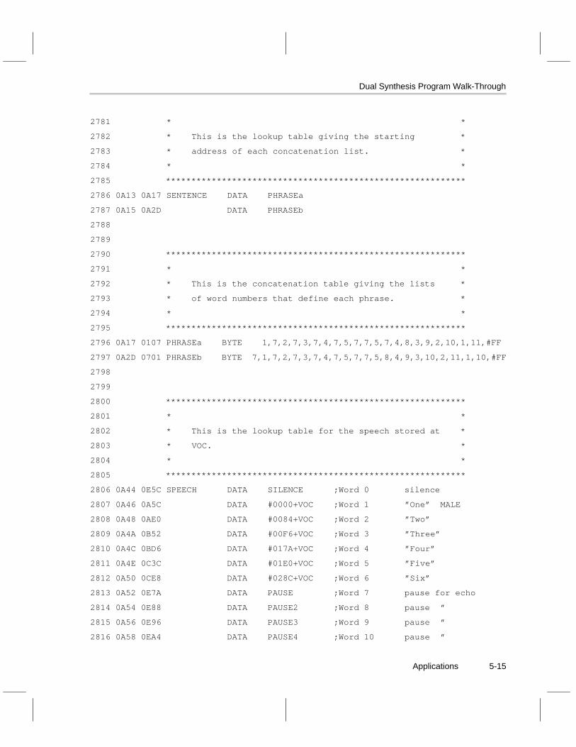
Dual Synthesis Program Walk-Through
5-15 Applications
2781 * *
2782 * This is the lookup table giving the starting *
2783 * address of each concatenation list. *
2784 * *
2785 ***********************************************************
2786 0A13 0A17 SENTENCE DATA PHRASEa
2787 0A15 0A2D DATA PHRASEb
2788
2789
2790 ***********************************************************
2791 * *
2792 * This is the concatenation table giving the lists *
2793 * of word numbers that define each phrase. *
2794 * *
2795 ***********************************************************
2796 0A17 0107 PHRASEa BYTE 1,7,2,7,3,7,4,7,5,7,7,5,7,4,8,3,9,2,10,1,11,#FF
2797 0A2D 0701 PHRASEb BYTE 7,1,7,2,7,3,7,4,7,5,7,7,5,8,4,9,3,10,2,11,1,10,#FF
2798
2799
2800 ***********************************************************
2801 * *
2802 * This is the lookup table for the speech stored at *
2803 * VOC. *
2804 * *
2805 ***********************************************************
2806 0A44 0E5C SPEECH DATA SILENCE ;Word 0 silence
2807 0A46 0A5C DATA #0000+VOC ;Word 1 ”One” MALE
2808 0A48 0AE0 DATA #0084+VOC ;Word 2 ”Two”
2809 0A4A 0B52 DATA #00F6+VOC ;Word 3 ”Three”
2810 0A4C 0BD6 DATA #017A+VOC ;Word 4 ”Four”
2811 0A4E 0C3C DATA #01E0+VOC ;Word 5 ”Five”
2812 0A50 0CE8 DATA #028C+VOC ;Word 6 ”Six”
2813 0A52 0E7A DATA PAUSE ;Word 7 pause for echo
2814 0A54 0E88 DATA PAUSE2 ;Word 8 pause ”
2815 0A56 0E96 DATA PAUSE3 ;Word 9 pause ”
2816 0A58 0EA4 DATA PAUSE4 ;Word 10 pause ”
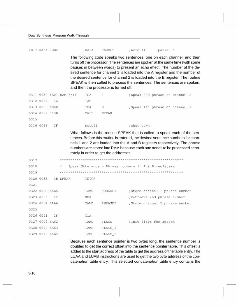
Dual Synthesis Program Walk-Through
5-16
2817 0A5A 0EB2 DATA PAUSE5 ;Word 11 pause ”
The following code speaks two sentences, one on each channel, and thenturns off the processor. The sentences are spoken at the same time (with somepauses in between words) to present an echo effect. The number of the de-sired sentence for channel 1 is loaded into the A register and the number ofthe desired sentence for channel 2 is loaded into the B register. The routineSPEAK is then called to process the sentences. The sentences are spoken,and then the processor is turned off.
0311 0032 6E01 RAM_EXIT TCA 1 ;Speak 2nd phrase on channel 2
0312 0034 1A TAB
0313 0035 6E00 TCA 0 ;Speak 1st phrase on channel 1
0314 0037 003B CALL SPEAK
0315
0316 0039 3F setoff ;shut down
What follows is the routine SPEAK that is called to speak each of the sen-tences. Before this routine is entered, the desired sentence numbers for chan-nels 1 and 2 are loaded into the A and B registers respectively. The phrasenumbers are stored into RAM because each one needs to be processed sepa-rately in order to get the addresses.
0317 ***********************************************************
0318 * Speak Utterance – Phrase numbers in A & B registers
0319 ***********************************************************
0320 003B 3B SPEAK INTGR
0321
0322 003C 6A65 TAMD PHRASE1 ;Store channel 1 phrase number
0323 003E 12 XBA ;retrieve 2nd phrase number
0324 003F 6A66 TAMD PHRASE2 ;Store channel 2 phrase number
0325
0326 0041 2F CLA
0327 0042 6A62 TAMD FLAGS ;Init flags for speech
0328 0044 6A63 TAMD FLAGS_1
0329 0046 6A64 TAMD FLAGS_2
Because each sentence pointer is two bytes long, the sentence number isdoubled to get the correct offset into the sentence pointer table. This offset isadded to the start address of the table to get the address of the table entry. TheLUAA and LUAB instructions are used to get the two byte address of the con-catenation table entry. This selected concatenation table entry contains the
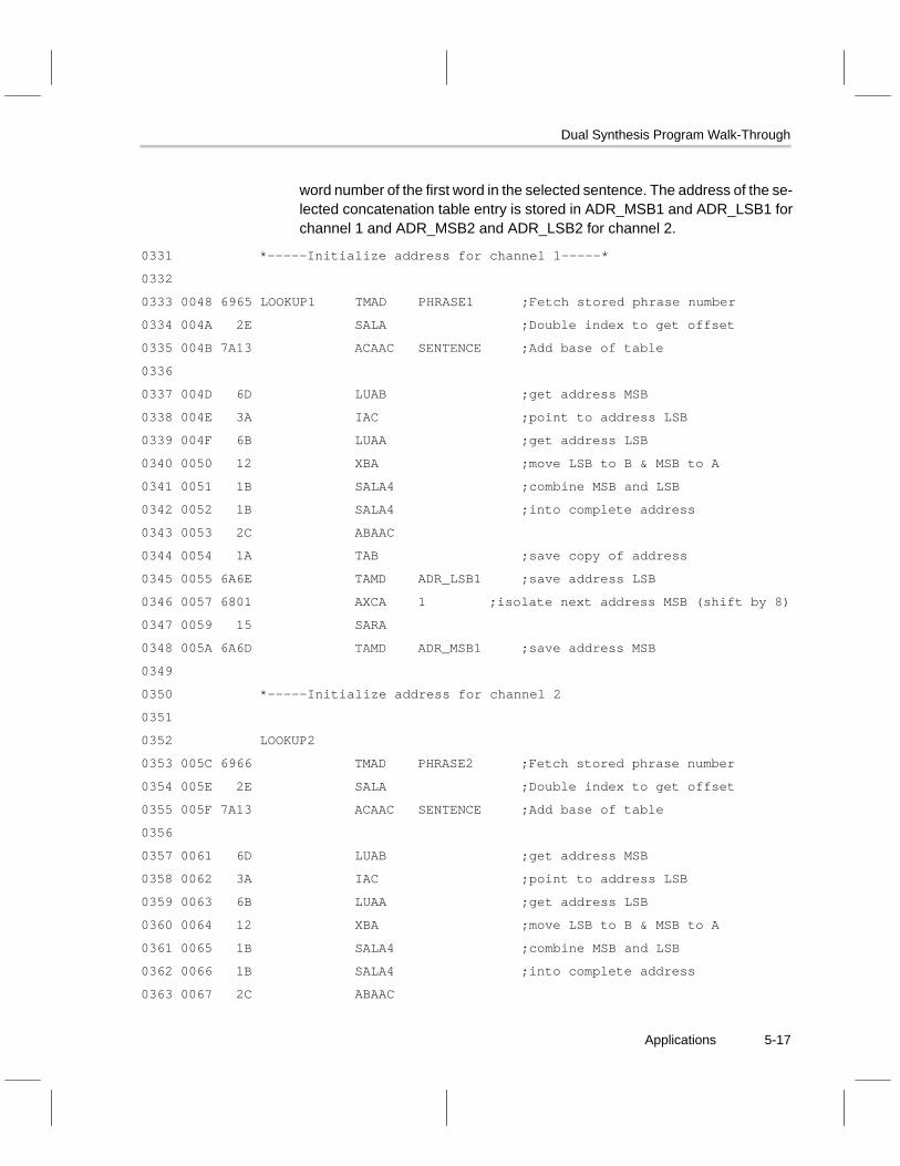
Dual Synthesis Program Walk-Through
5-17 Applications
word number of the first word in the selected sentence. The address of the se-lected concatenation table entry is stored in ADR_MSB1 and ADR_LSB1 forchannel 1 and ADR_MSB2 and ADR_LSB2 for channel 2.
0331 *–––––Initialize address for channel 1–––––*
0332
0333 0048 6965 LOOKUP1 TMAD PHRASE1 ;Fetch stored phrase number
0334 004A 2E SALA ;Double index to get offset
0335 004B 7A13 ACAAC SENTENCE ;Add base of table
0336
0337 004D 6D LUAB ;get address MSB
0338 004E 3A IAC ;point to address LSB
0339 004F 6B LUAA ;get address LSB
0340 0050 12 XBA ;move LSB to B & MSB to A
0341 0051 1B SALA4 ;combine MSB and LSB
0342 0052 1B SALA4 ;into complete address
0343 0053 2C ABAAC
0344 0054 1A TAB ;save copy of address
0345 0055 6A6E TAMD ADR_LSB1 ;save address LSB
0346 0057 6801 AXCA 1 ;isolate next address MSB (shift by 8)
0347 0059 15 SARA
0348 005A 6A6D TAMD ADR_MSB1 ;save address MSB
0349
0350 *–––––Initialize address for channel 2
0351
0352 LOOKUP2
0353 005C 6966 TMAD PHRASE2 ;Fetch stored phrase number
0354 005E 2E SALA ;Double index to get offset
0355 005F 7A13 ACAAC SENTENCE ;Add base of table
0356
0357 0061 6D LUAB ;get address MSB
0358 0062 3A IAC ;point to address LSB
0359 0063 6B LUAA ;get address LSB
0360 0064 12 XBA ;move LSB to B & MSB to A
0361 0065 1B SALA4 ;combine MSB and LSB
0362 0066 1B SALA4 ;into complete address
0363 0067 2C ABAAC
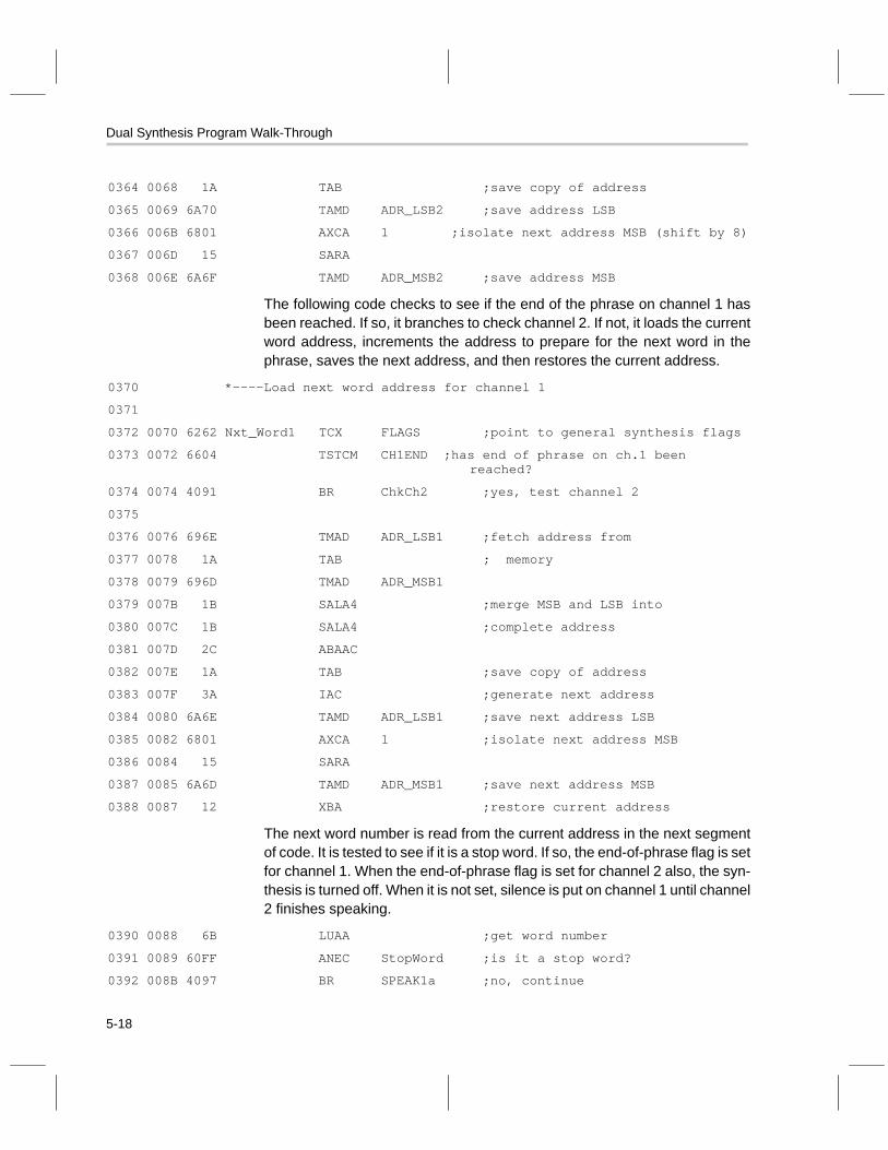
Dual Synthesis Program Walk-Through
5-18
0364 0068 1A TAB ;save copy of address
0365 0069 6A70 TAMD ADR_LSB2 ;save address LSB
0366 006B 6801 AXCA 1 ;isolate next address MSB (shift by 8)
0367 006D 15 SARA
0368 006E 6A6F TAMD ADR_MSB2 ;save address MSB
The following code checks to see if the end of the phrase on channel 1 hasbeen reached. If so, it branches to check channel 2. If not, it loads the currentword address, increments the address to prepare for the next word in thephrase, saves the next address, and then restores the current address.
0370 *––––Load next word address for channel 1
0371
0372 0070 6262 Nxt_Word1 TCX FLAGS ;point to general synthesis flags
0373 0072 6604 TSTCM CH1END ;has end of phrase on ch.1 been reached?
0374 0074 4091 BR ChkCh2 ;yes, test channel 2
0375
0376 0076 696E TMAD ADR_LSB1 ;fetch address from
0377 0078 1A TAB ; memory
0378 0079 696D TMAD ADR_MSB1
0379 007B 1B SALA4 ;merge MSB and LSB into
0380 007C 1B SALA4 ;complete address
0381 007D 2C ABAAC
0382 007E 1A TAB ;save copy of address
0383 007F 3A IAC ;generate next address
0384 0080 6A6E TAMD ADR_LSB1 ;save next address LSB
0385 0082 6801 AXCA 1 ;isolate next address MSB
0386 0084 15 SARA
0387 0085 6A6D TAMD ADR_MSB1 ;save next address MSB
0388 0087 12 XBA ;restore current address
The next word number is read from the current address in the next segmentof code. It is tested to see if it is a stop word. If so, the end-of-phrase flag is setfor channel 1. When the end-of-phrase flag is set for channel 2 also, the syn-thesis is turned off. When it is not set, silence is put on channel 1 until channel2 finishes speaking.
0390 0088 6B LUAA ;get word number
0391 0089 60FF ANEC StopWord ;is it a stop word?
0392 008B 4097 BR SPEAK1a ;no, continue
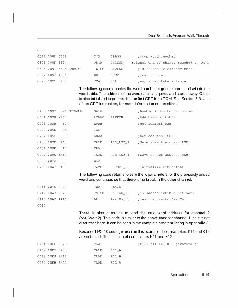
Dual Synthesis Program Walk-Through
5-19 Applications
0393
0394 008D 6262 TCX FLAGS ;stop word reached
0395 008F 6404 ORCM CH1END ;signal end of phrase reached on ch.1
0396 0091 6608 ChkCh2 TSTCM CH2END ;is channel 2 already done?
0397 0093 4604 BR STOP ;yes, return
0398 0095 6E00 TCA SIL ;no, substitute silence
The following code doubles the word number to get the correct offset into theword table. The address of the word data is acquired and stored away. Offsetis also initialized to prepare for the first GET from ROM. See Section 5.8, Useof the GET Instruction, for more information on the offset.
0400 0097 2E SPEAK1a SALA ;Double index to get offset
0401 0098 7A44 ACAAC SPEECH ;Add base of table
0402 009A 6D LUAB ;get address MSB
0403 009B 3A IAC
0404 009C 6B LUAA ;Get address LSB
0405 009D 6A68 TAMD ADR_LSB_1 ;Save speech address LSB
0406 009F 12 XBA
0407 00A0 6A67 TAMD ADR_MSB_1 ;Save speech address MSB
0408 00A2 2F CLA
0409 00A3 6A69 TAMD OFFSET_1 ;Initialize bit offset
The following code returns to zero the K parameters for the previously endedword and continues so that there is no break in the other channel.
0411 00A5 6262 TCX FLAGS
0412 00A7 6620 TSTCM Ch1Inh_2 ;is second inhibit bit set?
0413 00A9 44AC BR ZeroKs_1b ;yes, return to ZeroKs
0414
There is also a routine to load the next word address for channel 2(Nxt_Word2). This code is similar to the above code for channel 1, so it is notdiscussed here. It can be seen in the complete program listing in Appendix C.
Because LPC-10 coding is used in this example, the parameters K11 and K12are not used. This section of code clears K11 and K12.
0461 00E6 2F CLA ;Kill K11 and K12 parameters
0462 00E7 6A03 TAMD K11_A
0463 00E9 6A13 TAMD K11_B
0464 00EB 6A02 TAMD K12_A
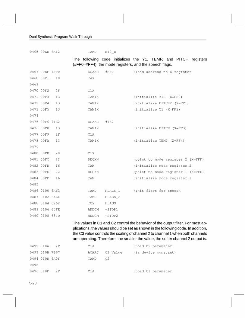
Dual Synthesis Program Walk-Through
5-20
0465 00ED 6A12 TAMD K12_B
The following code initializes the Y1, TEMP, and PITCH registers(#FF0–#FF4), the mode registers, and the speech flags.
0467 00EF 7FF0 ACAAC #FF0 ;load address to X register
0468 00F1 18 TAX
0469
0470 00F2 2F CLA
0471 00F3 13 TAMIX ;initialize Y1S (X=FF0)
0472 00F4 13 TAMIX ;initialize PITCH2 (X=FF1)
0473 00F5 13 TAMIX ;initialize Y1 (X=FF2)
0474
0475 00F6 7162 ACAAC #162
0476 00F8 13 TAMIX ;initialize PITCH (X=FF3)
0477 00F9 2F CLA
0478 00FA 13 TAMIX ;initialize TEMP (X=FF4)
0479
0480 00FB 20 CLX
0481 00FC 22 DECXN ;point to mode register 2 (X=FFF)
0482 00FD 16 TAM ;initialize mode register 2
0483 00FE 22 DECXN ;point to mode register 1 (X=FFE)
0484 00FF 16 TAM ;initialize mode register 1
0485
0486 0100 6A63 TAMD FLAGS_1 ;Init flags for speech
0487 0102 6A64 TAMD FLAGS_2
0488 0104 6262 TCX FLAGS
0489 0106 65FE ANDCM ~STOP1
0490 0108 65FD ANDCM ~STOP2
The values in C1 and C2 control the behavior of the output filter. For most ap-plications, the values should be set as shown in the following code. In addition,the C3 value controls the scaling of channel 2 to channel 1 when both channelsare operating. Therefore, the smaller the value, the softer channel 2 output is.
0492 010A 2F CLA ;Load C2 parameter
0493 010B 7B67 ACAAC C2_Value ;(a device constant)
0494 010D 6A0F TAMD C2
0495
0496 010F 2F CLA ;Load C1 parameter
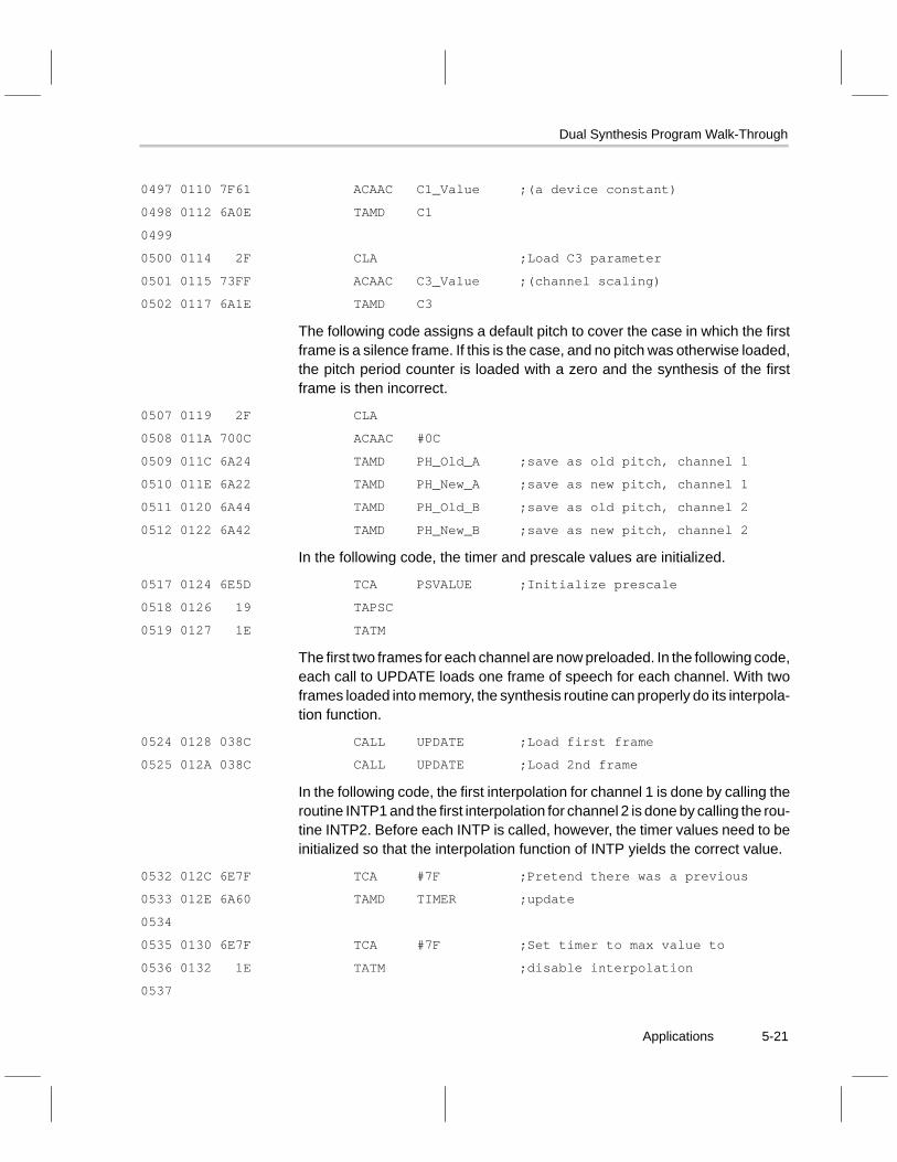
Dual Synthesis Program Walk-Through
5-21 Applications
0497 0110 7F61 ACAAC C1_Value ;(a device constant)
0498 0112 6A0E TAMD C1
0499
0500 0114 2F CLA ;Load C3 parameter
0501 0115 73FF ACAAC C3_Value ;(channel scaling)
0502 0117 6A1E TAMD C3
The following code assigns a default pitch to cover the case in which the firstframe is a silence frame. If this is the case, and no pitch was otherwise loaded,the pitch period counter is loaded with a zero and the synthesis of the firstframe is then incorrect.
0507 0119 2F CLA
0508 011A 700C ACAAC #0C
0509 011C 6A24 TAMD PH_Old_A ;save as old pitch, channel 1
0510 011E 6A22 TAMD PH_New_A ;save as new pitch, channel 1
0511 0120 6A44 TAMD PH_Old_B ;save as old pitch, channel 2
0512 0122 6A42 TAMD PH_New_B ;save as new pitch, channel 2
In the following code, the timer and prescale values are initialized.
0517 0124 6E5D TCA PSVALUE ;Initialize prescale
0518 0126 19 TAPSC
0519 0127 1E TATM
The first two frames for each channel are now preloaded. In the following code,each call to UPDATE loads one frame of speech for each channel. With twoframes loaded into memory, the synthesis routine can properly do its interpola-tion function.
0524 0128 038C CALL UPDATE ;Load first frame
0525 012A 038C CALL UPDATE ;Load 2nd frame
In the following code, the first interpolation for channel 1 is done by calling theroutine INTP1 and the first interpolation for channel 2 is done by calling the rou-tine INTP2. Before each INTP is called, however, the timer values need to beinitialized so that the interpolation function of INTP yields the correct value.
0532 012C 6E7F TCA #7F ;Pretend there was a previous
0533 012E 6A60 TAMD TIMER ;update
0534
0535 0130 6E7F TCA #7F ;Set timer to max value to
0536 0132 1E TATM ;disable interpolation
0537
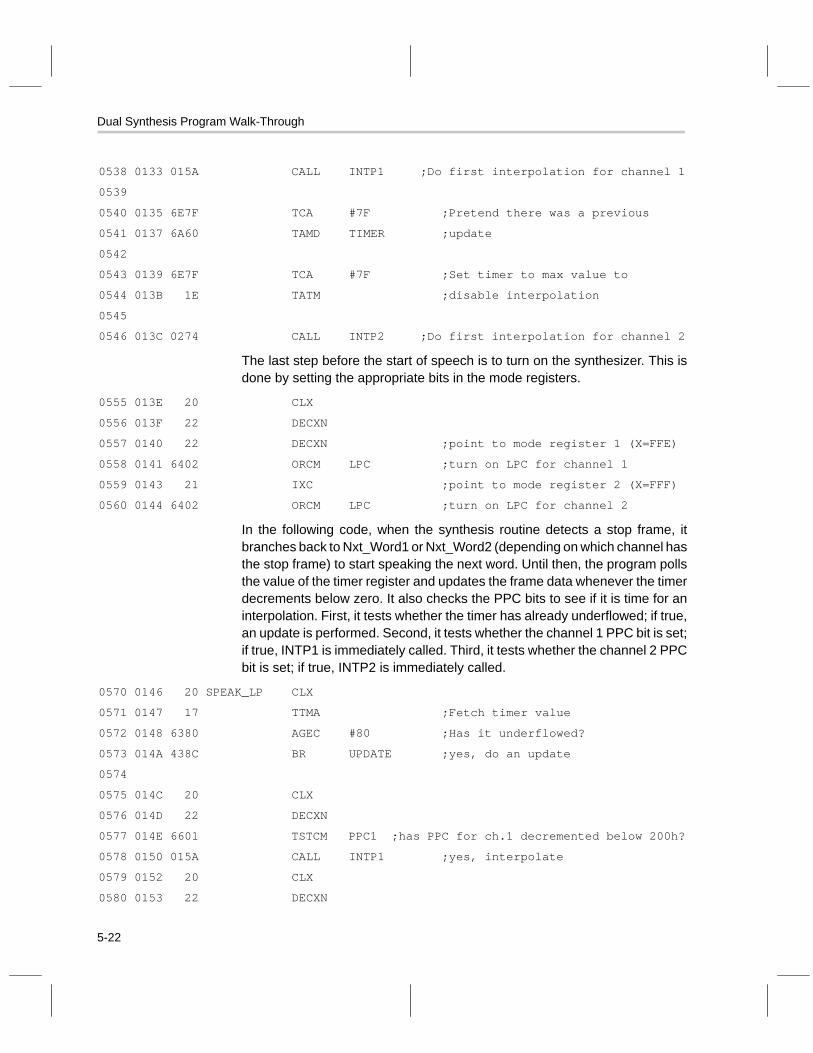
Dual Synthesis Program Walk-Through
5-22
0538 0133 015A CALL INTP1 ;Do first interpolation for channel 1
0539
0540 0135 6E7F TCA #7F ;Pretend there was a previous
0541 0137 6A60 TAMD TIMER ;update
0542
0543 0139 6E7F TCA #7F ;Set timer to max value to
0544 013B 1E TATM ;disable interpolation
0545
0546 013C 0274 CALL INTP2 ;Do first interpolation for channel 2
The last step before the start of speech is to turn on the synthesizer. This isdone by setting the appropriate bits in the mode registers.
0555 013E 20 CLX
0556 013F 22 DECXN
0557 0140 22 DECXN ;point to mode register 1 (X=FFE)
0558 0141 6402 ORCM LPC ;turn on LPC for channel 1
0559 0143 21 IXC ;point to mode register 2 (X=FFF)
0560 0144 6402 ORCM LPC ;turn on LPC for channel 2
In the following code, when the synthesis routine detects a stop frame, itbranches back to Nxt_Word1 or Nxt_Word2 (depending on which channel hasthe stop frame) to start speaking the next word. Until then, the program pollsthe value of the timer register and updates the frame data whenever the timerdecrements below zero. It also checks the PPC bits to see if it is time for aninterpolation. First, it tests whether the timer has already underflowed; if true,an update is performed. Second, it tests whether the channel 1 PPC bit is set;if true, INTP1 is immediately called. Third, it tests whether the channel 2 PPCbit is set; if true, INTP2 is immediately called.
0570 0146 20 SPEAK_LP CLX
0571 0147 17 TTMA ;Fetch timer value
0572 0148 6380 AGEC #80 ;Has it underflowed?
0573 014A 438C BR UPDATE ;yes, do an update
0574
0575 014C 20 CLX
0576 014D 22 DECXN
0577 014E 6601 TSTCM PPC1 ;has PPC for ch.1 decremented below 200h?
0578 0150 015A CALL INTP1 ;yes, interpolate
0579 0152 20 CLX
0580 0153 22 DECXN
Dual Synthesis Program Walk-Through
5-23 Applications
0581 0154 6608 TSTCM PPC2 ;has PPC for ch.2 decremented below 200h?
0582 0156 0274 CALL INTP2 ;yes, interpolate
0583 0158 4146 BR SPEAK_LP ;no, wait some more
The following routine, INTP1, is the interpolation routine for channel 1. The in-terpolation routine for channel 2 (INTP2) is similar to this one; therefore, onlyINTP1 is discussed in this chapter. The routine INTP2 can be found within thecomplete program in Appendix C.
In the following code, INTP1 is reached whenever the pitch period counter forchannel 1 decrements below 200h. Its purpose is to do any necessary inter-polation of the reflection coefficients (K parameters) and to load the result intothe working registers.
On entry to INTP1, the PPC1 bit is cleared to reset, and the CHANNEL bit iscleared to select channel 1.
0591 015A 20 INTP1 CLX
0592 015B 22 DECXN ;point to Mode Register 2
0593 015C 65FE ANDCM ~PPC1 ;reset PPC1 bit
0594 015E 65EF ANDCM ~CHANNEL ;select channel 1
If a word has just been loaded (besides the first word in a phrase), then twoframes must be loaded by UPDATE before interpolation can occur. The follow-ing code checks to see if those two frames have been loaded yet (inhibit bits1 and 2 are cleared when ready). If not, the energy must be cleared and INTP1must be exited.
0600 0160 6262 TCX FLAGS
0601 0162 6620 TSTCM Ch1Inh_2 ;is second inhibit bit set?
0602 0164 4168 BR INTP1a ;yes, not ready for interpolation yet
0603 0166 416D BR INTP1b ;no, continue with interpolation
0604
0605 INTP1a
0606 0168 2F CLA ;clear energy while waiting
0607 0169 6A01 TAMD EN_A
0608 016B 4272 BR IRETI1 ;return from call
In the following code, the current value of the timer register is stored. This valueis used later when interpolation is performed.
0610 016D 17 INTP1b TTMA ;Get timer register contents
0611 016E 6380 AGEC #80 ;Has timer underflowed?
0612 0170 4174 BR Adjust1 ;yes, Trick Scale to avoid problems
Dual Synthesis Program Walk-Through
5-24
0613 0172 4175 BR DoScale1 ;no, Use Timer as is
0614
0615 0174 2F Adjust1 CLA ;Pretend no underflow
0616 0175 6A61 DoScale1 TAMD SCALE ;Load timer val into scale
When interpolation has been turned off by the UPDATE routine, INTP is exited.This is shown in the following code.
0622 0177 6263 TCX FLAGS_1 ;Point to channel 1 flags
0623 0179 6601 TSTCM Int_Off ;If routine disabled...
0624 017B 4272 BR IRETI1 ;...branch to exit point
If there is a transition between a voiced frame and an unvoiced frame, then nointerpolation should be performed between the two frames because the K pa-rameters of a voiced frame are not compatible with the K parameters of an un-voiced frame. Any transition between frame types is detected in the UPDATEroutine and signaled by setting the Int_Inh bit in FLAGS_1. The following codetests FLAGS_1 to see if interpolation should be performed between frames.
0632 017D 6263 TINTP1 TCX FLAGS_1 ;Point to channel 1 status flags
0633 017F 6620 TSTCM Int_Inh ;Is interpolation inhibited?
0634 0181 4185 BR NOINT1 ;yes, use inhibit code
0635 0183 41A4 BR INTPCH1 ;no, use interpolation code
The following code is reached if interpolation is inhibited. It sets the stored val-ue of the timer register to 7F, which effectively forces the interpolation to yieldthe old values for the working values, thereby effectively disabling interpola-tion.
0643 0185 6E7F NOINT1 TCA #7F ;Set Scale factor to
0644 0187 6A61 TAMD SCALE ;highest value
If there is a transition between a voiced and an unvoiced frame, the energyneeds to be cleared until the K parameters and the unvoiced bit in the moderegister all have been updated. This prevents the processor’s LPC filter fromusing a mixture of voiced and unvoiced parameters. If the unvoiced bit in themode register does not match the unvoiced bit in FLAGS_1, the energy iscleared. This is done in the following code.
0654 0189 6263 TCX FLAGS_1
0655 018B 6680 TSTCM Unv_Flg_Old ;Is new frame unvoiced?
0656 018D 4198 BR Uv1 ;yes, go to unvoiced branch
0657
0658 018F 20 CLX
0659 0190 22 DECXN ;point to Mode Register 1
Dual Synthesis Program Walk-Through
5-25 Applications
0660 0191 22 DECXN ;New frame is voiced
0661 0192 6680 TSTCM UNV ;Has mode changed to unvoiced
0662 0194 419F BR ClrEN1 ;yes, clear the energy
0663 0196 41A4 BR INTPCH1 ;no, no action required
0664
0665 0198 20 Uv1 CLX ;New frame is unvoiced
0666 0199 22 DECXN
0667 019A 22 DECXN
0668 019B 6680 TSTCM UNV ;Has voicing mode changed?
0669 019D 41A4 BR INTPCH1 ;no, no action required
0670
0671 019F 2F ClrEN1 CLA ;Zero Energy during update
0672 01A0 6A01 TAMD EN_A
0673 01A2 41A4 BR INTPCH1
We are now ready to do the interpolation. Interpolation is done at this point withthe standard linear equation:
y = mx + b
rewritten to:
P = (Pcurrent – Pnew) × TIMER + Pnew
where:
P = interpolated parameter
Pcurrent = value of parameter in current frame
Pnew = value of parameter in new frame
TIMER = value in TIMER
The multiplication using the AXMA function scales the result by 080h. Thevalue in TIMER ranges from 07Fh to 000h. When interpolation is inhibited,TIMER contains 07Fh and the interpolation results in P = Pcurrent.
The following code interpolates pitch. Pitch (as well as K1 and K2) is storedusing two bytes. The program reads the most significant byte, left shifts it byone nibble, and then adds the least significant nibble of the value (stored in thesecond byte). The result is a 12-bit value. This is done both for the current andnew values.
Unlike the K parameters, decoded pitch is always positive. The INTGR instruc-tion at the start of INTP1 ensures the integer mode so that when the program
Dual Synthesis Program Walk-Through
5-26
gets the decoded pitch from the decoding tables, it is not sign extended. SeeSection 5.4, Arithmetic Modes, for additional information on the integer and ex-tended-sign modes.
0679 01A4 6222 INTPCH1 TCX PH_New_A ;Combine new pitch and fractional
0680 01A6 14 TMAIX ;pitch and leave in
0681 01A7 1B SALA4 ;the B register
0682 01A8 28 AMAAC
0683 01A9 21 IXC
0684 01AA 1A TAB
0685 01AB 14 TMAIX ;Combine current pitch and
0686 01AC 1B SALA4 ; current fractional pitch
0687 01AD 28 AMAAC ; and leave in A register
0688
0689 01AE 2D SBAAN ;(Pcurrent – Pnew)
0690 01AF 6261 TCX SCALE
0691 01B1 39 AXMA ;(Pcurrent – Pnew) * Timer
0692 01B2 2C ABAAC ;Pnew + (Pcurrent – Pnew)* Timer
Unlike the other speech parameters, the interpolated pitch is not written toRAM. Instead, it is written to the pitch register using the TASYN instruction. Inthis particular code, the TASYN is commented out to avoid clicking. The pitchis loaded directly to the pitch register (X = #FF3). Because the value in the PPCis used to address the excitation function values, each of which is two byteslong, the interpolated pitch needs to be multiplied by two before writing it to thePPC. This is done in the following code using the SALA instruction.
0693 01B3 2E SALA ;Double value to index excitation
0694
0695 ** TASYN ;Write to pitch register
0696
0697 01B4 1A tab ;Write to pitch register (#FF3)
0698 01B5 2F cla ;NOTE: TASYN instruction causes problems
0699 01B6 7FF3 acaac #ff3 ;so we must write directly to
0700 01B8 18 tax ;the pitch register
0701 01B9 12 xba
0702 01BA 16 tam
The decoded energy, like the pitch, is always positive. The following code inter-polates the energy.
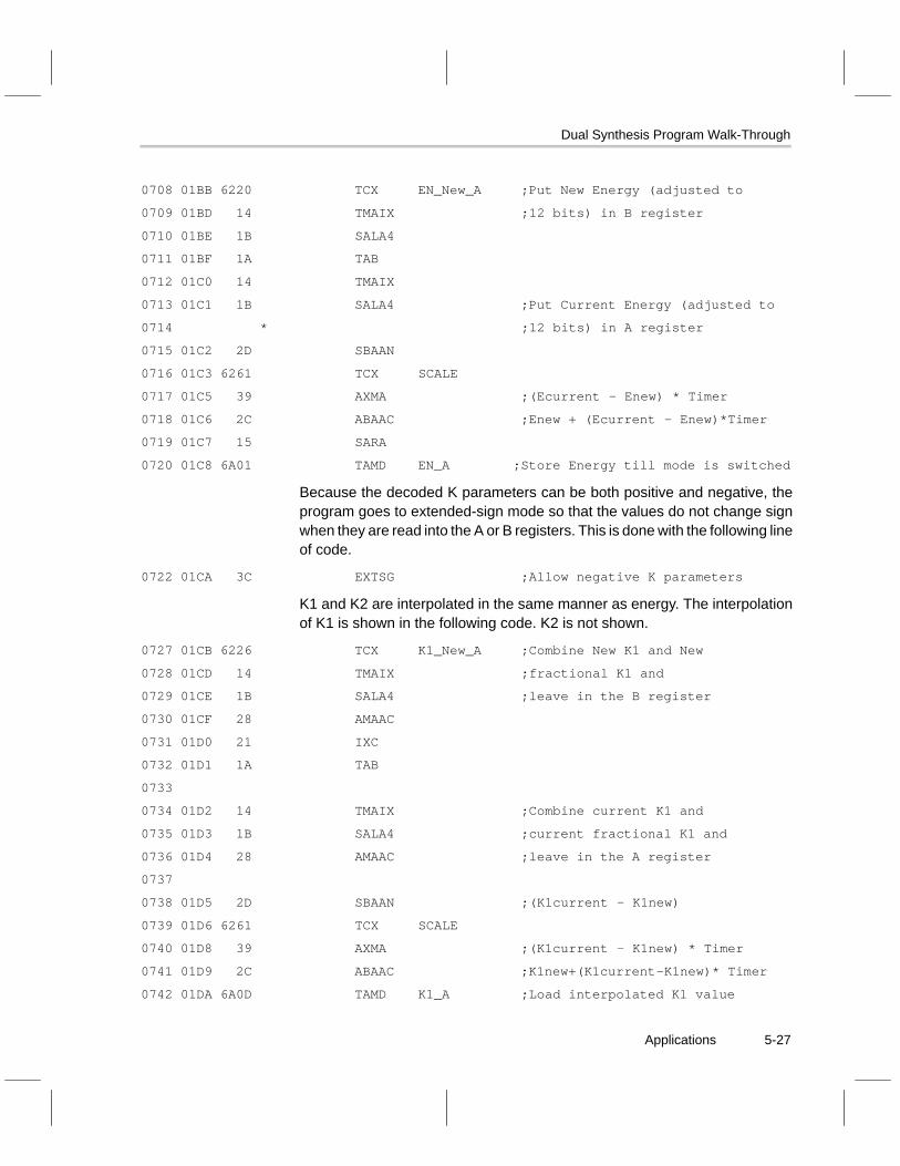
Dual Synthesis Program Walk-Through
5-27 Applications
0708 01BB 6220 TCX EN_New_A ;Put New Energy (adjusted to
0709 01BD 14 TMAIX ;12 bits) in B register
0710 01BE 1B SALA4
0711 01BF 1A TAB
0712 01C0 14 TMAIX
0713 01C1 1B SALA4 ;Put Current Energy (adjusted to
0714 * ;12 bits) in A register
0715 01C2 2D SBAAN
0716 01C3 6261 TCX SCALE
0717 01C5 39 AXMA ;(Ecurrent – Enew) * Timer
0718 01C6 2C ABAAC ;Enew + (Ecurrent – Enew)*Timer
0719 01C7 15 SARA
0720 01C8 6A01 TAMD EN_A ;Store Energy till mode is switched
Because the decoded K parameters can be both positive and negative, theprogram goes to extended-sign mode so that the values do not change signwhen they are read into the A or B registers. This is done with the following lineof code.
0722 01CA 3C EXTSG ;Allow negative K parameters
K1 and K2 are interpolated in the same manner as energy. The interpolationof K1 is shown in the following code. K2 is not shown.
0727 01CB 6226 TCX K1_New_A ;Combine New K1 and New
0728 01CD 14 TMAIX ;fractional K1 and
0729 01CE 1B SALA4 ;leave in the B register
0730 01CF 28 AMAAC
0731 01D0 21 IXC
0732 01D1 1A TAB
0733
0734 01D2 14 TMAIX ;Combine current K1 and
0735 01D3 1B SALA4 ;current fractional K1 and
0736 01D4 28 AMAAC ;leave in the A register
0737
0738 01D5 2D SBAAN ;(K1current – K1new)
0739 01D6 6261 TCX SCALE
0740 01D8 39 AXMA ;(K1current – K1new) * Timer
0741 01D9 2C ABAAC ;K1new+(K1current–K1new)* Timer
0742 01DA 6A0D TAMD K1_A ;Load interpolated K1 value
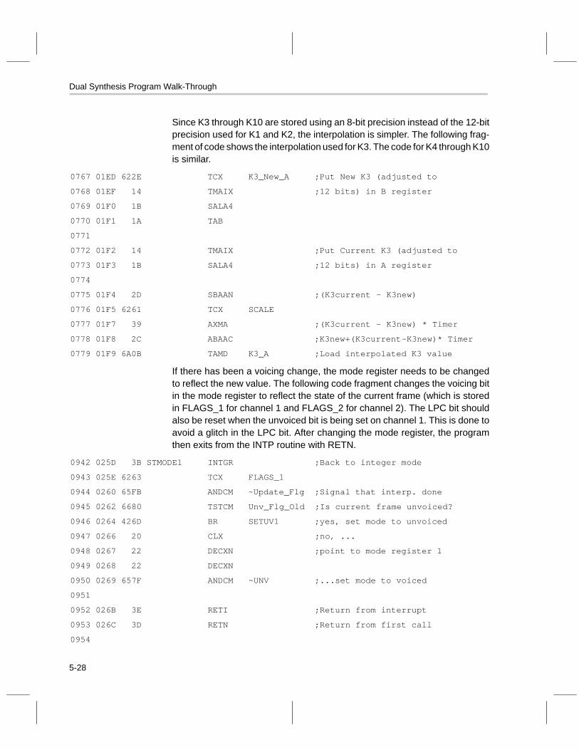
Dual Synthesis Program Walk-Through
5-28
Since K3 through K10 are stored using an 8-bit precision instead of the 12-bitprecision used for K1 and K2, the interpolation is simpler. The following frag-ment of code shows the interpolation used for K3. The code for K4 through K10is similar.
0767 01ED 622E TCX K3_New_A ;Put New K3 (adjusted to
0768 01EF 14 TMAIX ;12 bits) in B register
0769 01F0 1B SALA4
0770 01F1 1A TAB
0771
0772 01F2 14 TMAIX ;Put Current K3 (adjusted to
0773 01F3 1B SALA4 ;12 bits) in A register
0774
0775 01F4 2D SBAAN ;(K3current – K3new)
0776 01F5 6261 TCX SCALE
0777 01F7 39 AXMA ;(K3current – K3new) * Timer
0778 01F8 2C ABAAC ;K3new+(K3current–K3new)* Timer
0779 01F9 6A0B TAMD K3_A ;Load interpolated K3 value
If there has been a voicing change, the mode register needs to be changedto reflect the new value. The following code fragment changes the voicing bitin the mode register to reflect the state of the current frame (which is storedin FLAGS_1 for channel 1 and FLAGS_2 for channel 2). The LPC bit shouldalso be reset when the unvoiced bit is being set on channel 1. This is done toavoid a glitch in the LPC bit. After changing the mode register, the programthen exits from the INTP routine with RETN.
0942 025D 3B STMODE1 INTGR ;Back to integer mode
0943 025E 6263 TCX FLAGS_1
0944 0260 65FB ANDCM ~Update_Flg ;Signal that interp. done
0945 0262 6680 TSTCM Unv_Flg_Old ;Is current frame unvoiced?
0946 0264 426D BR SETUV1 ;yes, set mode to unvoiced
0947 0266 20 CLX ;no, ...
0948 0267 22 DECXN ;point to mode register 1
0949 0268 22 DECXN
0950 0269 657F ANDCM ~UNV ;...set mode to voiced
0951
0952 026B 3E RETI ;Return from interrupt
0953 026C 3D RETN ;Return from first call
0954
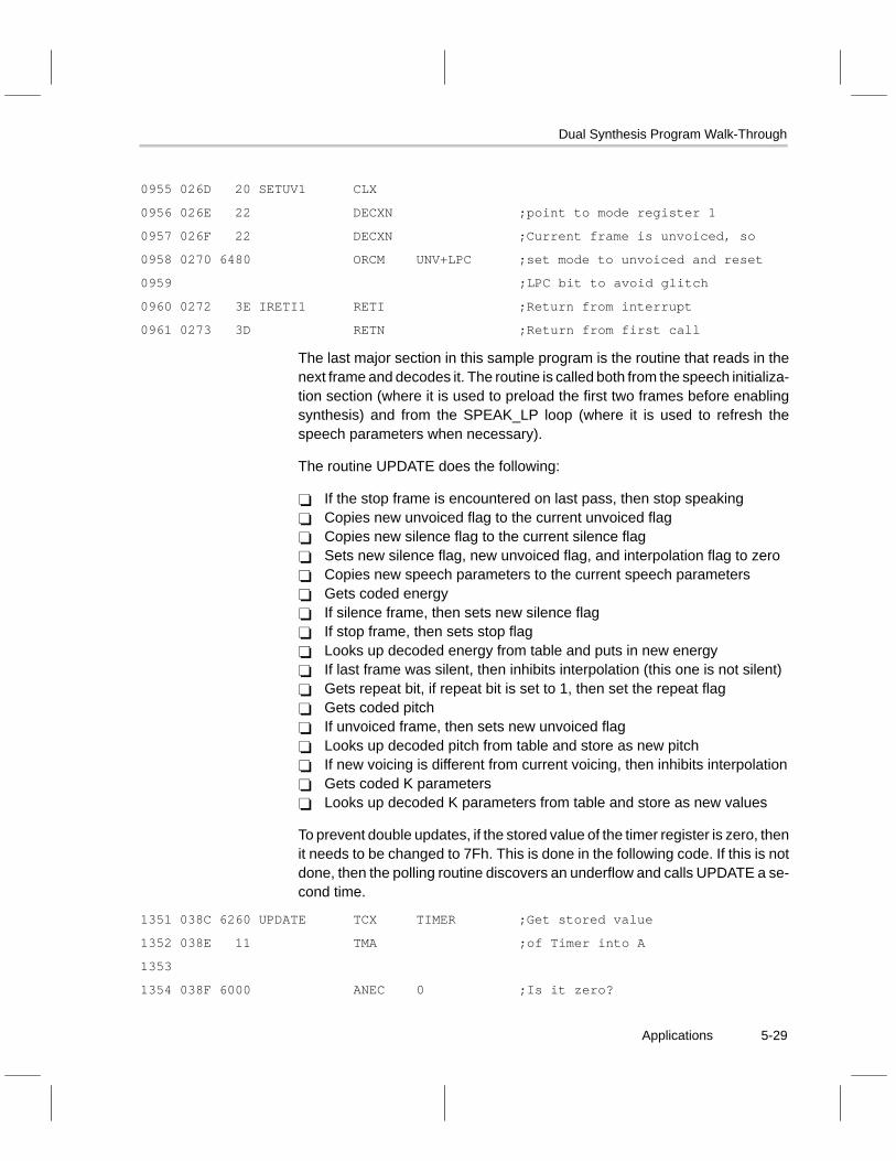
Dual Synthesis Program Walk-Through
5-29 Applications
0955 026D 20 SETUV1 CLX
0956 026E 22 DECXN ;point to mode register 1
0957 026F 22 DECXN ;Current frame is unvoiced, so
0958 0270 6480 ORCM UNV+LPC ;set mode to unvoiced and reset
0959 ;LPC bit to avoid glitch
0960 0272 3E IRETI1 RETI ;Return from interrupt
0961 0273 3D RETN ;Return from first call
The last major section in this sample program is the routine that reads in thenext frame and decodes it. The routine is called both from the speech initializa-tion section (where it is used to preload the first two frames before enablingsynthesis) and from the SPEAK_LP loop (where it is used to refresh thespeech parameters when necessary).
The routine UPDATE does the following:
If the stop frame is encountered on last pass, then stop speaking Copies new unvoiced flag to the current unvoiced flag Copies new silence flag to the current silence flag Sets new silence flag, new unvoiced flag, and interpolation flag to zero Copies new speech parameters to the current speech parameters Gets coded energy If silence frame, then sets new silence flag If stop frame, then sets stop flag Looks up decoded energy from table and puts in new energy If last frame was silent, then inhibits interpolation (this one is not silent) Gets repeat bit, if repeat bit is set to 1, then set the repeat flag Gets coded pitch If unvoiced frame, then sets new unvoiced flag Looks up decoded pitch from table and store as new pitch If new voicing is different from current voicing, then inhibits interpolation Gets coded K parameters Looks up decoded K parameters from table and store as new values
To prevent double updates, if the stored value of the timer register is zero, thenit needs to be changed to 7Fh. This is done in the following code. If this is notdone, then the polling routine discovers an underflow and calls UPDATE a se-cond time.
1351 038C 6260 UPDATE TCX TIMER ;Get stored value
1352 038E 11 TMA ;of Timer into A
1353
1354 038F 6000 ANEC 0 ;Is it zero?
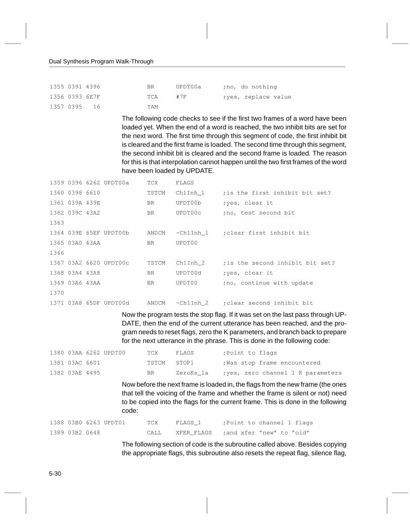
Dual Synthesis Program Walk-Through
5-30
1355 0391 4396 BR UPDT00a ;no, do nothing
1356 0393 6E7F TCA #7F ;yes, replace value
1357 0395 16 TAM
The following code checks to see if the first two frames of a word have beenloaded yet. When the end of a word is reached, the two inhibit bits are set forthe next word. The first time through this segment of code, the first inhibit bitis cleared and the first frame is loaded. The second time through this segment,the second inhibit bit is cleared and the second frame is loaded. The reasonfor this is that interpolation cannot happen until the two first frames of the wordhave been loaded by UPDATE.
1359 0396 6262 UPDT00a TCX FLAGS
1360 0398 6610 TSTCM Ch1Inh_1 ;is the first inhibit bit set?
1361 039A 439E BR UPDT00b ;yes, clear it
1362 039C 43A2 BR UPDT00c ;no, test second bit
1363
1364 039E 65EF UPDT00b ANDCM ~Ch1Inh_1 ;clear first inhibit bit
1365 03A0 43AA BR UPDT00
1366
1367 03A2 6620 UPDT00c TSTCM Ch1Inh_2 ;is the second inhibit bit set?
1368 03A4 43A8 BR UPDT00d ;yes, clear it
1369 03A6 43AA BR UPDT00 ;no, continue with update
1370
1371 03A8 65DF UPDT00d ANDCM ~Ch1Inh_2 ;clear second inhibit bit
Now the program tests the stop flag. If it was set on the last pass through UP-DATE, then the end of the current utterance has been reached, and the pro-gram needs to reset flags, zero the K parameters, and branch back to preparefor the next utterance in the phrase. This is done in the following code:
1380 03AA 6262 UPDT00 TCX FLAGS ;Point to flags
1381 03AC 6601 TSTCM STOP1 ;Was stop frame encountered
1382 03AE 4495 BR ZeroKs_1a ;yes, zero channel 1 K parameters
Now before the next frame is loaded in, the flags from the new frame (the onesthat tell the voicing of the frame and whether the frame is silent or not) needto be copied into the flags for the current frame. This is done in the followingcode:
1388 03B0 6263 UPDT01 TCX FLAGS_1 ;Point to channel 1 flags
1389 03B2 0648 CALL XFER_FLAGS ;and xfer ”new” to ”old”
The following section of code is the subroutine called above. Besides copyingthe appropriate flags, this subroutine also resets the repeat flag, silence flag,
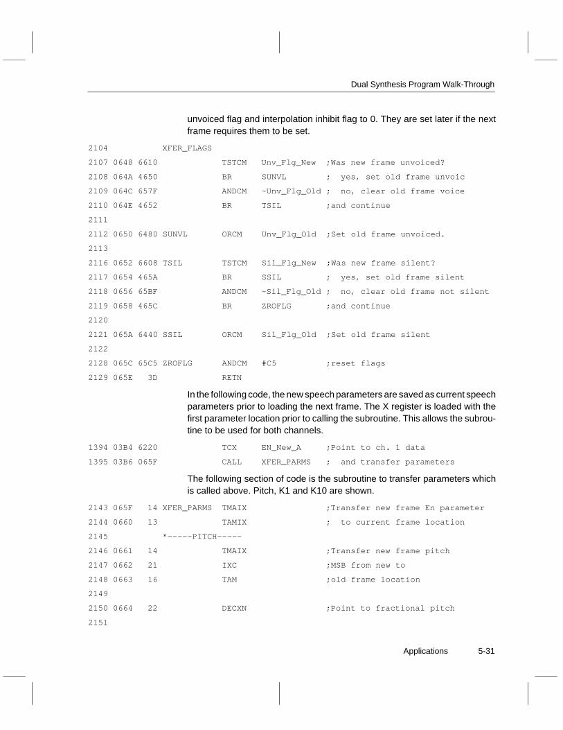
Dual Synthesis Program Walk-Through
5-31 Applications
unvoiced flag and interpolation inhibit flag to 0. They are set later if the nextframe requires them to be set.
2104 XFER_FLAGS
2107 0648 6610 TSTCM Unv_Flg_New ;Was new frame unvoiced?
2108 064A 4650 BR SUNVL ; yes, set old frame unvoic
2109 064C 657F ANDCM ~Unv_Flg_Old ; no, clear old frame voice
2110 064E 4652 BR TSIL ;and continue
2111
2112 0650 6480 SUNVL ORCM Unv_Flg_Old ;Set old frame unvoiced.
2113
2116 0652 6608 TSIL TSTCM Sil_Flg_New ;Was new frame silent?
2117 0654 465A BR SSIL ; yes, set old frame silent
2118 0656 65BF ANDCM ~Sil_Flg_Old ; no, clear old frame not silent
2119 0658 465C BR ZROFLG ;and continue
2120
2121 065A 6440 SSIL ORCM Sil_Flg_Old ;Set old frame silent
2122
2128 065C 65C5 ZROFLG ANDCM #C5 ;reset flags
2129 065E 3D RETN
In the following code, the new speech parameters are saved as current speechparameters prior to loading the next frame. The X register is loaded with thefirst parameter location prior to calling the subroutine. This allows the subrou-tine to be used for both channels.
1394 03B4 6220 TCX EN_New_A ;Point to ch. 1 data
1395 03B6 065F CALL XFER_PARMS ; and transfer parameters
The following section of code is the subroutine to transfer parameters whichis called above. Pitch, K1 and K10 are shown.
2143 065F 14 XFER_PARMS TMAIX ;Transfer new frame En parameter
2144 0660 13 TAMIX ; to current frame location
2145 *–––––PITCH–––––
2146 0661 14 TMAIX ;Transfer new frame pitch
2147 0662 21 IXC ;MSB from new to
2148 0663 16 TAM ;old frame location
2149
2150 0664 22 DECXN ;Point to fractional pitch
2151
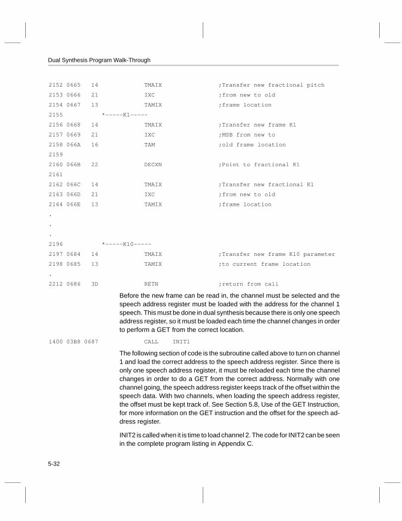
Dual Synthesis Program Walk-Through
5-32
2152 0665 14 TMAIX ;Transfer new fractional pitch
2153 0666 21 IXC ;from new to old
2154 0667 13 TAMIX ;frame location
2155 *–––––K1–––––
2156 0668 14 TMAIX ;Transfer new frame K1
2157 0669 21 IXC ;MSB from new to
2158 066A 16 TAM ;old frame location
2159
2160 066B 22 DECXN ;Point to fractional K1
2161
2162 066C 14 TMAIX ;Transfer new fractional K1
2163 066D 21 IXC ;from new to old
2164 066E 13 TAMIX ;frame location
.
.
.
2196 *–––––K10–––––
2197 0684 14 TMAIX ;Transfer new frame K10 parameter
2198 0685 13 TAMIX ;to current frame location
.
2212 0686 3D RETN ;return from call
Before the new frame can be read in, the channel must be selected and thespeech address register must be loaded with the address for the channel 1speech. This must be done in dual synthesis because there is only one speechaddress register, so it must be loaded each time the channel changes in orderto perform a GET from the correct location.
1400 03B8 0687 CALL INIT1
The following section of code is the subroutine called above to turn on channel1 and load the correct address to the speech address register. Since there isonly one speech address register, it must be reloaded each time the channelchanges in order to do a GET from the correct address. Normally with onechannel going, the speech address register keeps track of the offset within thespeech data. With two channels, when loading the speech address register,the offset must be kept track of. See Section 5.8, Use of the GET Instruction,for more information on the GET instruction and the offset for the speech ad-dress register.
INIT2 is called when it is time to load channel 2. The code for INIT2 can be seenin the complete program listing in Appendix C.
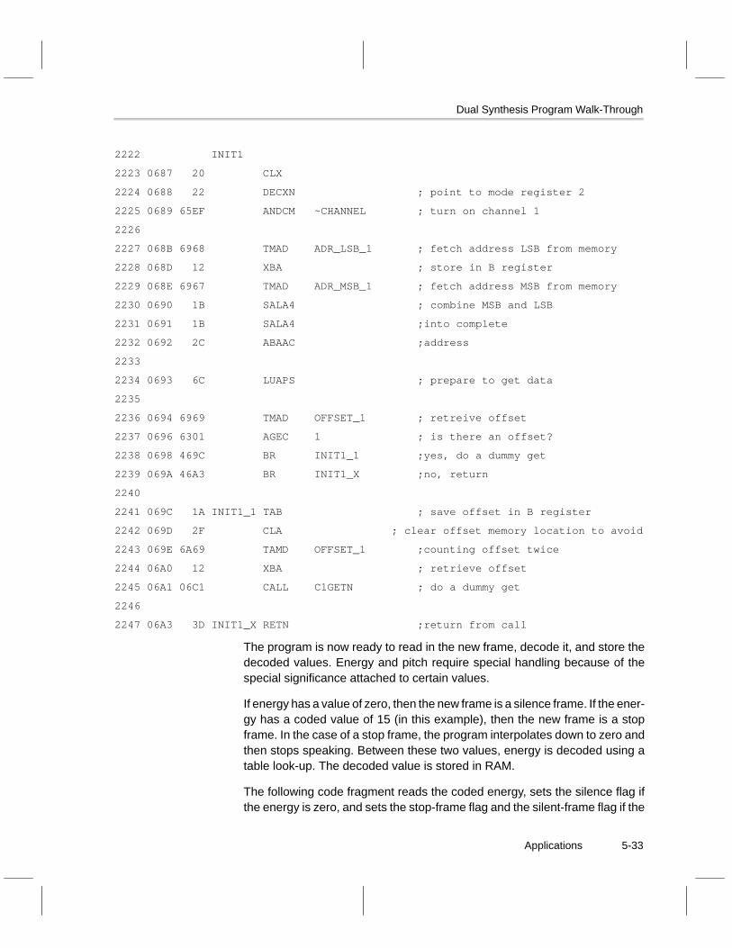
Dual Synthesis Program Walk-Through
5-33 Applications
2222 INIT1
2223 0687 20 CLX
2224 0688 22 DECXN ; point to mode register 2
2225 0689 65EF ANDCM ~CHANNEL ; turn on channel 1
2226
2227 068B 6968 TMAD ADR_LSB_1 ; fetch address LSB from memory
2228 068D 12 XBA ; store in B register
2229 068E 6967 TMAD ADR_MSB_1 ; fetch address MSB from memory
2230 0690 1B SALA4 ; combine MSB and LSB
2231 0691 1B SALA4 ;into complete
2232 0692 2C ABAAC ;address
2233
2234 0693 6C LUAPS ; prepare to get data
2235
2236 0694 6969 TMAD OFFSET_1 ; retreive offset
2237 0696 6301 AGEC 1 ; is there an offset?
2238 0698 469C BR INIT1_1 ;yes, do a dummy get
2239 069A 46A3 BR INIT1_X ;no, return
2240
2241 069C 1A INIT1_1 TAB ; save offset in B register
2242 069D 2F CLA ; clear offset memory location to avoid
2243 069E 6A69 TAMD OFFSET_1 ;counting offset twice
2244 06A0 12 XBA ; retrieve offset
2245 06A1 06C1 CALL C1GETN ; do a dummy get
2246
2247 06A3 3D INIT1_X RETN ;return from call
The program is now ready to read in the new frame, decode it, and store thedecoded values. Energy and pitch require special handling because of thespecial significance attached to certain values.
If energy has a value of zero, then the new frame is a silence frame. If the ener-gy has a coded value of 15 (in this example), then the new frame is a stopframe. In the case of a stop frame, the program interpolates down to zero andthen stops speaking. Between these two values, energy is decoded using atable look-up. The decoded value is stored in RAM.
The following code fragment reads the coded energy, sets the silence flag ifthe energy is zero, and sets the stop-frame flag and the silent-frame flag if the
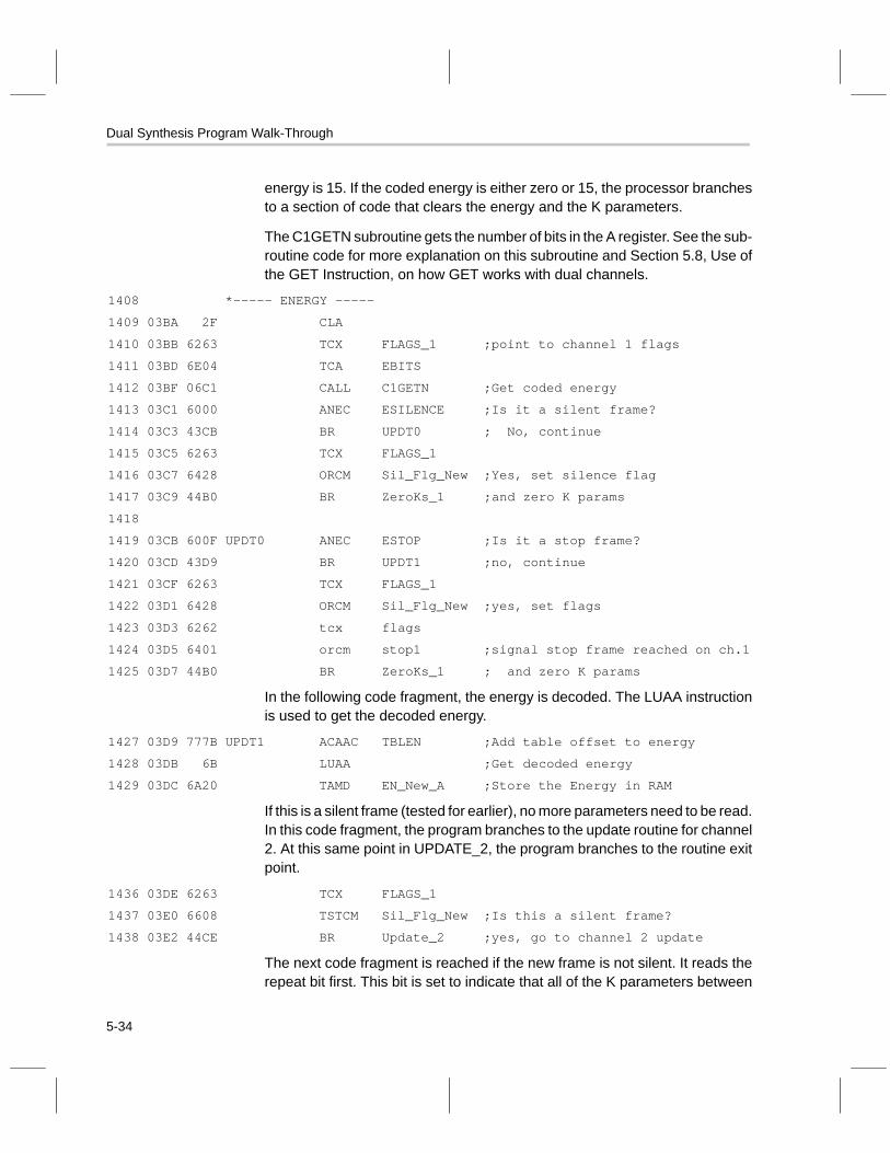
Dual Synthesis Program Walk-Through
5-34
energy is 15. If the coded energy is either zero or 15, the processor branchesto a section of code that clears the energy and the K parameters.
The C1GETN subroutine gets the number of bits in the A register. See the sub-routine code for more explanation on this subroutine and Section 5.8, Use ofthe GET Instruction, on how GET works with dual channels.
1408 *––––– ENERGY –––––
1409 03BA 2F CLA
1410 03BB 6263 TCX FLAGS_1 ;point to channel 1 flags
1411 03BD 6E04 TCA EBITS
1412 03BF 06C1 CALL C1GETN ;Get coded energy
1413 03C1 6000 ANEC ESILENCE ;Is it a silent frame?
1414 03C3 43CB BR UPDT0 ; No, continue
1415 03C5 6263 TCX FLAGS_1
1416 03C7 6428 ORCM Sil_Flg_New ;Yes, set silence flag
1417 03C9 44B0 BR ZeroKs_1 ;and zero K params
1418
1419 03CB 600F UPDT0 ANEC ESTOP ;Is it a stop frame?
1420 03CD 43D9 BR UPDT1 ;no, continue
1421 03CF 6263 TCX FLAGS_1
1422 03D1 6428 ORCM Sil_Flg_New ;yes, set flags
1423 03D3 6262 tcx flags
1424 03D5 6401 orcm stop1 ;signal stop frame reached on ch.1
1425 03D7 44B0 BR ZeroKs_1 ; and zero K params
In the following code fragment, the energy is decoded. The LUAA instructionis used to get the decoded energy.
1427 03D9 777B UPDT1 ACAAC TBLEN ;Add table offset to energy
1428 03DB 6B LUAA ;Get decoded energy
1429 03DC 6A20 TAMD EN_New_A ;Store the Energy in RAM
If this is a silent frame (tested for earlier), no more parameters need to be read.In this code fragment, the program branches to the update routine for channel2. At this same point in UPDATE_2, the program branches to the routine exitpoint.
1436 03DE 6263 TCX FLAGS_1
1437 03E0 6608 TSTCM Sil_Flg_New ;Is this a silent frame?
1438 03E2 44CE BR Update_2 ;yes, go to channel 2 update
The next code fragment is reached if the new frame is not silent. It reads therepeat bit first. This bit is set to indicate that all of the K parameters between
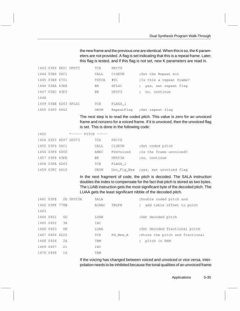
Dual Synthesis Program Walk-Through
5-35 Applications
the new frame and the previous one are identical. When this is so, the K param-eters are not provided. A flag is set indicating that this is a repeat frame. Later,this flag is tested, and if this flag is not set, new K parameters are read in.
1443 03E4 6E01 UPDT2 TCA RBITS
1444 03E6 06C1 CALL C1GETN ;Get the Repeat bit
1445 03E8 6701 TSTCA #01 ;Is this a repeat frame?
1446 03EA 43EE BR SFLG1 ; yes, set repeat flag
1447 03EC 43F2 BR UPDT3 ; no, continue
1448
1449 03EE 6263 SFLG1 TCX FLAGS_1
1450 03F0 6402 ORCM RepeatFlag ;Set repeat flag
The next step is to read the coded pitch. This value is zero for an unvoicedframe and nonzero for a voiced frame. If it is unvoiced, then the unvoiced flagis set. This is done in the following code:
1452 *––––– PITCH –––––
1454 03F2 6E07 UPDT3 TCA PBITS
1455 03F4 06C1 CALL C1GETN ;Get coded pitch
1456 03F6 6000 ANEC PUnVoiced ;Is the frame unvoiced?
1457 03F8 43FE BR UPDT3A ;no, continue
1458 03FA 6263 TCX FLAGS_1
1459 03FC 6410 ORCM Unv_Flg_New ;yes, set unvoiced flag
In the next fragment of code, the pitch is decoded. The SALA instructiondoubles the index to compensate for the fact that pitch is stored as two bytes.The LUAB instruction gets the most significant byte of the decoded pitch. TheLUAA gets the least significant nibble of the decoded pitch.
1461 03FE 2E UPDT3A SALA ;Double coded pitch and
1462 03FF 778B ACAAC TBLPH ; add table offset to point
1463
1464 0401 6D LUAB ;Get decoded pitch
1465 0402 3A IAC
1466 0403 6B LUAA ;Get decoded fractional pitch
1467 0404 6222 TCX PH_New_A ;Store the pitch and fractional
1468 0406 2A TBM ; pitch in RAM
1469 0407 21 IXC
1470 0408 16 TAM
If the voicing has changed between voiced and unvoiced or vice versa, inter-polation needs to be inhibited because the tonal qualities of an unvoiced frame
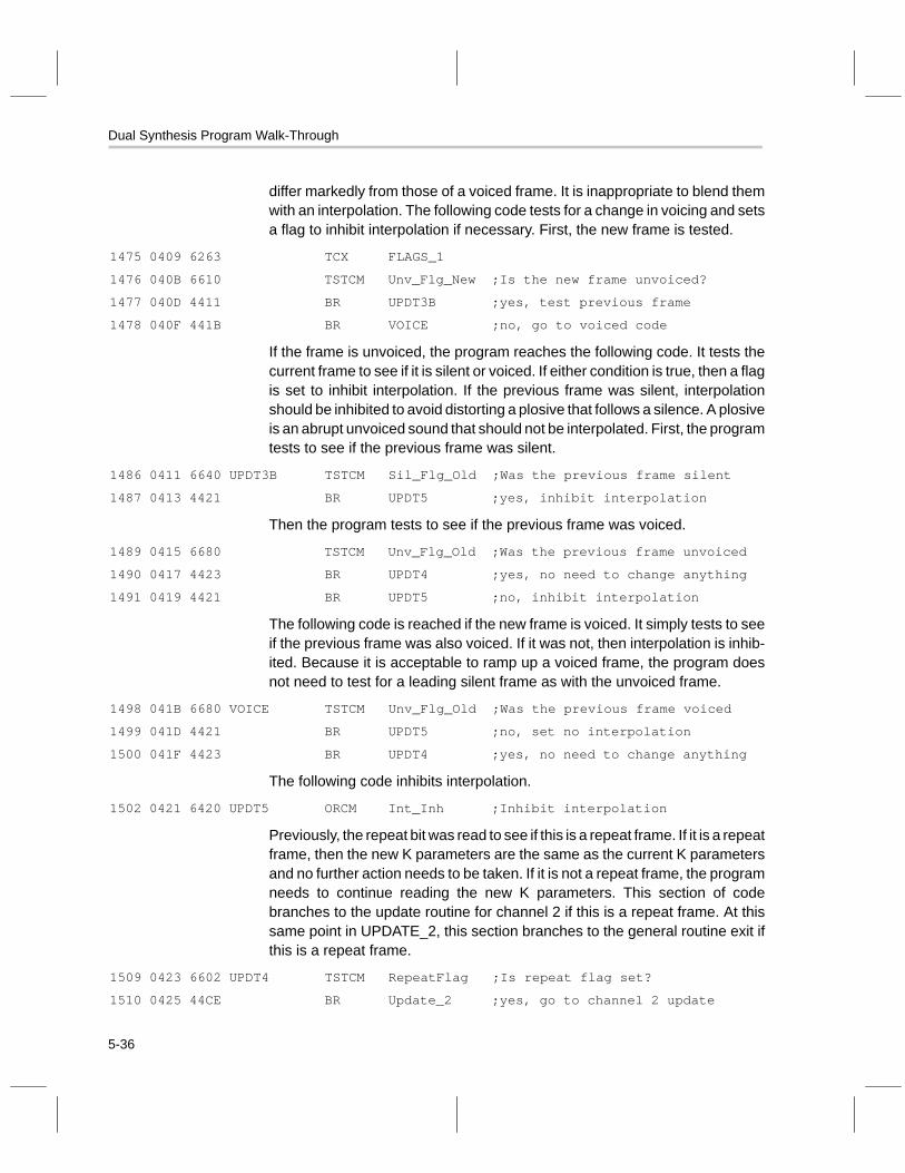
Dual Synthesis Program Walk-Through
5-36
differ markedly from those of a voiced frame. It is inappropriate to blend themwith an interpolation. The following code tests for a change in voicing and setsa flag to inhibit interpolation if necessary. First, the new frame is tested.
1475 0409 6263 TCX FLAGS_1
1476 040B 6610 TSTCM Unv_Flg_New ;Is the new frame unvoiced?
1477 040D 4411 BR UPDT3B ;yes, test previous frame
1478 040F 441B BR VOICE ;no, go to voiced code
If the frame is unvoiced, the program reaches the following code. It tests thecurrent frame to see if it is silent or voiced. If either condition is true, then a flagis set to inhibit interpolation. If the previous frame was silent, interpolationshould be inhibited to avoid distorting a plosive that follows a silence. A plosiveis an abrupt unvoiced sound that should not be interpolated. First, the programtests to see if the previous frame was silent.
1486 0411 6640 UPDT3B TSTCM Sil_Flg_Old ;Was the previous frame silent
1487 0413 4421 BR UPDT5 ;yes, inhibit interpolation
Then the program tests to see if the previous frame was voiced.
1489 0415 6680 TSTCM Unv_Flg_Old ;Was the previous frame unvoiced
1490 0417 4423 BR UPDT4 ;yes, no need to change anything
1491 0419 4421 BR UPDT5 ;no, inhibit interpolation
The following code is reached if the new frame is voiced. It simply tests to seeif the previous frame was also voiced. If it was not, then interpolation is inhib-ited. Because it is acceptable to ramp up a voiced frame, the program doesnot need to test for a leading silent frame as with the unvoiced frame.
1498 041B 6680 VOICE TSTCM Unv_Flg_Old ;Was the previous frame voiced
1499 041D 4421 BR UPDT5 ;no, set no interpolation
1500 041F 4423 BR UPDT4 ;yes, no need to change anything
The following code inhibits interpolation.
1502 0421 6420 UPDT5 ORCM Int_Inh ;Inhibit interpolation
Previously, the repeat bit was read to see if this is a repeat frame. If it is a repeatframe, then the new K parameters are the same as the current K parametersand no further action needs to be taken. If it is not a repeat frame, the programneeds to continue reading the new K parameters. This section of codebranches to the update routine for channel 2 if this is a repeat frame. At thissame point in UPDATE_2, this section branches to the general routine exit ifthis is a repeat frame.
1509 0423 6602 UPDT4 TSTCM RepeatFlag ;Is repeat flag set?
1510 0425 44CE BR Update_2 ;yes, go to channel 2 update
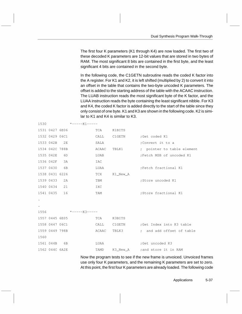
Dual Synthesis Program Walk-Through
5-37 Applications
The first four K parameters (K1 through K4) are now loaded. The first two ofthese decoded K parameters are 12-bit values that are stored in two bytes ofRAM. The most significant 8 bits are contained in the first byte, and the leastsignificant 4 bits are contained in the second byte.
In the following code, the C1GETN subroutine reads the coded K factor intothe A register. For K1 and K2, it is left shifted (multiplied by 2) to convert it intoan offset in the table that contains the two-byte uncoded K parameters. Theoffset is added to the starting address of the table with the ACAAC instruction.The LUAB instruction reads the most significant byte of the K factor, and theLUAA instruction reads the byte containing the least significant nibble. For K3and K4, the coded K factor is added directly to the start of the table since theyonly consist of one byte. K1 and K3 are shown in the following code. K2 is simi-lar to K1 and K4 is similar to K3.
1530 *–––––K1–––––
1531 0427 6E06 TCA K1BITS
1532 0429 06C1 CALL C1GETN ;Get coded K1
1533 042B 2E SALA ;Convert it to a
1534 042C 788B ACAAC TBLK1 ; pointer to table element
1535 042E 6D LUAB ;Fetch MSB of uncoded K1
1536 042F 3A IAC
1537 0430 6B LUAA ;Fetch fractional K1
1538 0431 6226 TCX K1_New_A
1539 0433 2A TBM ;Store uncoded K1
1540 0434 21 IXC
1541 0435 16 TAM ;Store fractional K1
.
.
1556 *–––––K3–––––
1557 0445 6E05 TCA K3BITS
1558 0447 06C1 CALL C1GETN ;Get Index into K3 table
1559 0449 798B ACAAC TBLK3 ; and add offset of table
1560
1561 044B 6B LUAA ;Get uncoded K3
1562 044C 6A2E TAMD K3_New_A ;and store it in RAM
Now the program tests to see if the new frame is unvoiced. Unvoiced framesuse only four K parameters, and the remaining K parameters are set to zero.At this point, the first four K parameters are already loaded. The following code
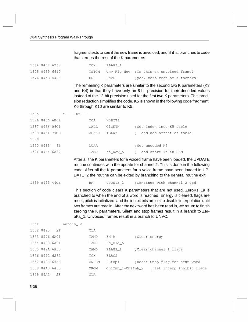
Dual Synthesis Program Walk-Through
5-38
fragment tests to see if the new frame is unvoiced, and, if it is, branches to codethat zeroes the rest of the K parameters.
1574 0457 6263 TCX FLAGS_1
1575 0459 6610 TSTCM Unv_Flg_New ;Is this an unvoiced frame?
1576 045B 44BF BR UNVC ;yes, zero rest of K factors
The remaining K parameters are similar to the second two K parameters (K3and K4) in that they have only an 8-bit precision for their decoded valuesinstead of the 12-bit precision used for the first two K parameters. This preci-sion reduction simplifies the code. K5 is shown in the following code fragment.K6 through K10 are similar to K5.
1585 *–––––K5–––––
1586 045D 6E04 TCA K5BITS
1587 045F 06C1 CALL C1GETN ;Get Index into K5 table
1588 0461 79CB ACAAC TBLK5 ; and add offset of table
1589
1590 0463 6B LUAA ;Get uncoded K5
1591 0464 6A32 TAMD K5_New_A ; and store it in RAM
After all the K parameters for a voiced frame have been loaded, the UPDATEroutine continues with the update for channel 2. This is done in the followingcode. After all the K parameters for a voice frame have been loaded in UP-DATE_2 the routine can be exited by branching to the general routine exit.
1639 0493 44CE BR UPDATE_2 ;Continue with channel 2 upd
This section of code clears K parameters that are not used. ZeroKs_1a isbranched to when the end of a word is reached. Energy is cleared, flags arereset, pitch is initialized, and the inhibit bits are set to disable interpolation untiltwo frames are read in. After the next word has been read in, we return to finishzeroing the K parameters. Silent and stop frames result in a branch to Zer-oKs_1. Unvoiced frames result in a branch to UNVC.
1651 ZeroKs_1a
1652 0495 2F CLA
1653 0496 6A01 TAMD EN_A ;Clear energy
1654 0498 6A21 TAMD EN_Old_A
1655 049A 6A63 TAMD FLAGS_1 ;Clear channel 1 flags
1656 049C 6262 TCX FLAGS
1657 049E 65FE ANDCM ~Stop1 ;Reset Stop flag for next word
1658 04A0 6430 ORCM Ch1Inh_1+Ch1Inh_2 ;Set interp inhibit flags
1659 04A2 2F CLA
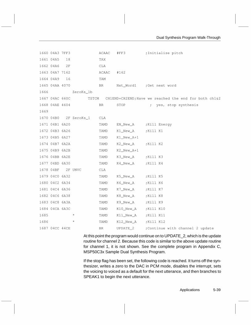
Dual Synthesis Program Walk-Through
5-39 Applications
1660 04A3 7FF3 ACAAC #FF3 ;Initialize pitch
1661 04A5 18 TAX
1662 04A6 2F CLA
1663 04A7 7162 ACAAC #162
1664 04A9 16 TAM
1665 04AA 4070 BR Nxt_Word1 ;Get next word
1666 ZeroKs_1b
1667 04AC 660C TSTCM CH1END+CH2END;Have we reached the end for both ch1&2
1668 04AE 4604 BR STOP ; yes, stop synthesis
1669
1670 04B0 2F ZeroKs_1 CLA
1671 04B1 6A20 TAMD EN_New_A ;Kill Energy
1672 04B3 6A26 TAMD K1_New_A ;Kill K1
1673 04B5 6A27 TAMD K1_New_A+1
1674 04B7 6A2A TAMD K2_New_A ;Kill K2
1675 04B9 6A2B TAMD K2_New_A+1
1676 04BB 6A2E TAMD K3_New_A ;Kill K3
1677 04BD 6A30 TAMD K4_New_A ;Kill K4
1678 04BF 2F UNVC CLA
1679 04C0 6A32 TAMD K5_New_A ;Kill K5
1680 04C2 6A34 TAMD K6_New_A ;Kill K6
1681 04C4 6A36 TAMD K7_New_A ;Kill K7
1682 04C6 6A38 TAMD K8_New_A ;Kill K8
1683 04C8 6A3A TAMD K9_New_A ;Kill K9
1684 04CA 6A3C TAMD K10_New_A ;Kill K10
1685 * TAMD K11_New_A ;Kill K11
1686 * TAMD K12_New_A ;Kill K12
1687 04CC 44CE BR UPDATE_2 ;Continue with channel 2 update
At this point the program would continue on to UPDATE_2, which is the updateroutine for channel 2. Because this code is similar to the above update routinefor channel 1, it is not shown. See the complete program in Appendix C,MSP50C3x Sample Dual Synthesis Program.
If the stop flag has been set, the following code is reached. It turns off the syn-thesizer, writes a zero to the DAC in PCM mode, disables the interrupt, setsthe voicing to voiced as a default for the next utterance, and then branches toSPEAK1 to begin the next utterance.
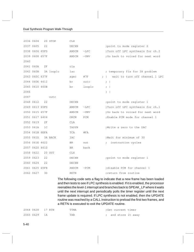
Dual Synthesis Program Walk-Through
5-40
2036 0604 20 STOP CLX
2037 0605 22 DECXN ;point to mode register 2
2038 0606 65FD ANDCM ~LPC ;Turn off LPC synthesis for ch.2
2039 0608 657F ANDCM ~UNV ;Go back to voiced for next word
2040
2041 060A 2F cla
2042 060B 3A loop1c iac ; temporary fix for 3X problem
2043 060C 637F agec #7F ; | wait to turn off channel 1 LPC
2044 060E 4612 br outc ; |
2045 0610 460B br loop1c ; |
2046 ; |
2047 outc
2048 0612 22 DECXN ;point to mode register 1
2049 0613 65FD ANDCM ~LPC ;Turn off LPC synthesis for ch.1
2050 0615 657F ANDCM ~UNV ;Go back to voiced for next word
2051 0617 6404 ORCM PCM ;Enable PCM mode for channel 1
2052 0619 2F CLA
2053 061A 1C TASYN ;Write a zero to the DAC
2054 061B 6EFA TCA #FA
2055 061D 3A BACK IAC ;Wait for minimum of 30
2056 061E 4622 BR out ; instruction cycles
2057 0620 461D BR back
2058 0622 20 OUT CLX
2059 0623 22 DECXN ;point to mode register 1
2060 0624 22 DECXN
2061 0625 65FB ANDCM ~PCM ;disable PCM for channel 1
2062 0627 3D RETN ;return from routine
The following code sets a flag to indicate that a new frame has been loadedand then tests to see if LPC synthesis is enabled. If it is enabled, the processorreenables the level-1 interrupt and branches back to SPEAK_LP where it waitsuntil the next interrupt and periodically polls the timer register until the nextframe update is required. If LPC synthesis is not enabled, then the UPDATEroutine was reached by a CALL instruction to preload the first two frames, anda RETN is executed to exit the UPDATE routine.
2064 0628 17 RTN TTMA ;Get current timer
2065 0629 1A TAB ; and store it away
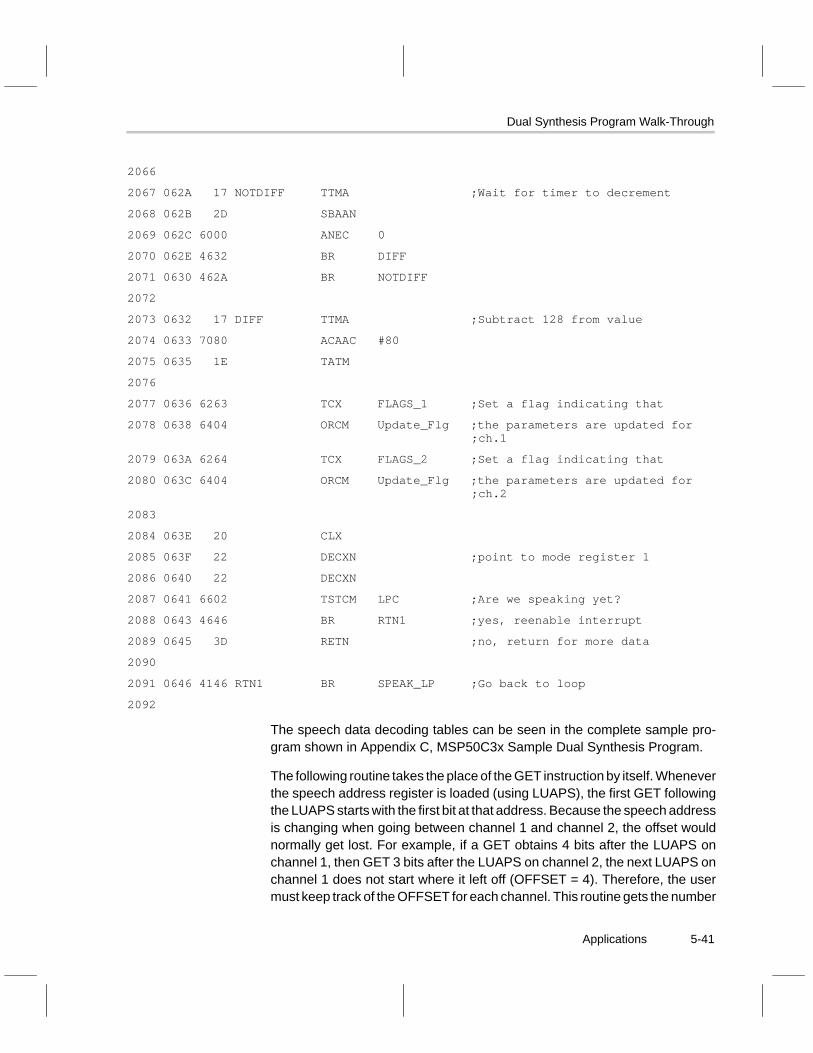
Dual Synthesis Program Walk-Through
5-41 Applications
2066
2067 062A 17 NOTDIFF TTMA ;Wait for timer to decrement
2068 062B 2D SBAAN
2069 062C 6000 ANEC 0
2070 062E 4632 BR DIFF
2071 0630 462A BR NOTDIFF
2072
2073 0632 17 DIFF TTMA ;Subtract 128 from value
2074 0633 7080 ACAAC #80
2075 0635 1E TATM
2076
2077 0636 6263 TCX FLAGS_1 ;Set a flag indicating that
2078 0638 6404 ORCM Update_Flg ;the parameters are updated for ;ch.1
2079 063A 6264 TCX FLAGS_2 ;Set a flag indicating that
2080 063C 6404 ORCM Update_Flg ;the parameters are updated for ;ch.2
2083
2084 063E 20 CLX
2085 063F 22 DECXN ;point to mode register 1
2086 0640 22 DECXN
2087 0641 6602 TSTCM LPC ;Are we speaking yet?
2088 0643 4646 BR RTN1 ;yes, reenable interrupt
2089 0645 3D RETN ;no, return for more data
2090
2091 0646 4146 RTN1 BR SPEAK_LP ;Go back to loop
2092
The speech data decoding tables can be seen in the complete sample pro-gram shown in Appendix C, MSP50C3x Sample Dual Synthesis Program.
The following routine takes the place of the GET instruction by itself. Wheneverthe speech address register is loaded (using LUAPS), the first GET followingthe LUAPS starts with the first bit at that address. Because the speech addressis changing when going between channel 1 and channel 2, the offset wouldnormally get lost. For example, if a GET obtains 4 bits after the LUAPS onchannel 1, then GET 3 bits after the LUAPS on channel 2, the next LUAPS onchannel 1 does not start where it left off (OFFSET = 4). Therefore, the usermust keep track of the OFFSET for each channel. This routine gets the number
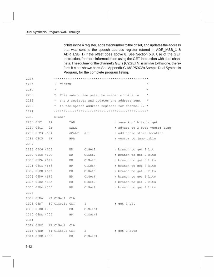
Dual Synthesis Program Walk-Through
5-42
of bits in the A register, adds that number to the offset, and updates the addressthat was sent to the speech address register (stored in ADR_MSB_1 &ADR_LSB_1) if the offset goes above 8. See Section 5.8, Use of the GETInstruction, for more information on using the GET instruction with dual chan-nels. The routine for the channel 2 GETs (C2GETN) is similar to this one, there-fore, it is not shown here. See Appendix C, MSP50C3x Sample Dual SynthesisProgram, for the complete program listing.
2285 **************************************************
2286 * C1GETN *
2287 * *
2288 * This subroutine gets the number of bits in *
2289 * the A register and updates the address sent *
2290 * to the speech address register for channel 1. *
2291 **************************************************
2292 C1GETN
2293 06C1 1A TAB ; save # of bits to get
2294 06C2 2E SALA ; adjust to 2 byte vector size
2295 06C3 76C4 ACAAC $+1 ; add table start location
2296 06C5 1F BRA ; vector to jump table
2297
2298 06C6 46D6 BR C1Get1 ; branch to get 1 bit
2299 06C8 46DC BR C1Get2 ; branch to get 2 bits
2300 06CA 46E2 BR C1Get3 ; branch to get 3 bits
2301 06CC 46E8 BR C1Get4 ; branch to get 4 bits
2302 06CE 46EE BR C1Get5 ; branch to get 5 bits
2303 06D0 46F4 BR C1Get6 ; branch to get 6 bits
2304 06D2 46FA BR C1Get7 ; branch to get 7 bits
2305 06D4 4700 BR C1Get8 ; branch to get 8 bits
2306
2307 06D6 2F C1Get1 CLA
2308 06D7 30 C1Get1a GET 1 ; get 1 bit
2309 06D8 4706 BR C1GetN1
2310 06DA 4706 BR C1GetN1
2311
2312 06DC 2F C1Get2 CLA
2313 06DD 31 C1Get2a GET 2 ; get 2 bits
2314 06DE 4706 BR C1GetN1
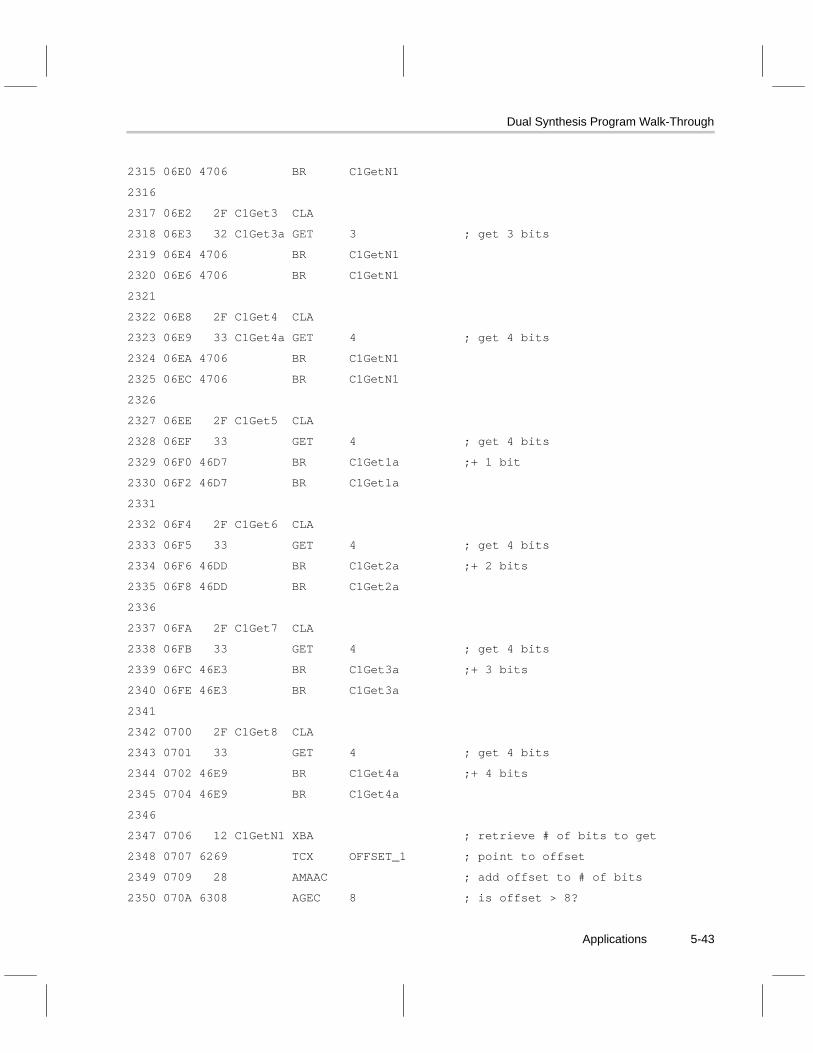
Dual Synthesis Program Walk-Through
5-43 Applications
2315 06E0 4706 BR C1GetN1
2316
2317 06E2 2F C1Get3 CLA
2318 06E3 32 C1Get3a GET 3 ; get 3 bits
2319 06E4 4706 BR C1GetN1
2320 06E6 4706 BR C1GetN1
2321
2322 06E8 2F C1Get4 CLA
2323 06E9 33 C1Get4a GET 4 ; get 4 bits
2324 06EA 4706 BR C1GetN1
2325 06EC 4706 BR C1GetN1
2326
2327 06EE 2F C1Get5 CLA
2328 06EF 33 GET 4 ; get 4 bits
2329 06F0 46D7 BR C1Get1a ;+ 1 bit
2330 06F2 46D7 BR C1Get1a
2331
2332 06F4 2F C1Get6 CLA
2333 06F5 33 GET 4 ; get 4 bits
2334 06F6 46DD BR C1Get2a ;+ 2 bits
2335 06F8 46DD BR C1Get2a
2336
2337 06FA 2F C1Get7 CLA
2338 06FB 33 GET 4 ; get 4 bits
2339 06FC 46E3 BR C1Get3a ;+ 3 bits
2340 06FE 46E3 BR C1Get3a
2341
2342 0700 2F C1Get8 CLA
2343 0701 33 GET 4 ; get 4 bits
2344 0702 46E9 BR C1Get4a ;+ 4 bits
2345 0704 46E9 BR C1Get4a
2346
2347 0706 12 C1GetN1 XBA ; retrieve # of bits to get
2348 0707 6269 TCX OFFSET_1 ; point to offset
2349 0709 28 AMAAC ; add offset to # of bits
2350 070A 6308 AGEC 8 ; is offset > 8?
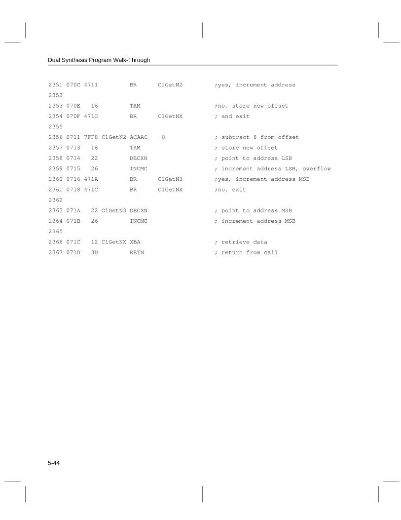
Dual Synthesis Program Walk-Through
5-44
2351 070C 4711 BR C1GetN2 ;yes, increment address
2352
2353 070E 16 TAM ;no, store new offset
2354 070F 471C BR C1GetNX ; and exit
2355
2356 0711 7FF8 C1GetN2 ACAAC –8 ; subtract 8 from offset
2357 0713 16 TAM ; store new offset
2358 0714 22 DECXN ; point to address LSB
2359 0715 26 INCMC ; increment address LSB, overflow
2360 0716 471A BR C1GetN3 ;yes, increment address MSB
2361 0718 471C BR C1GetNX ;no, exit
2362
2363 071A 22 C1GetN3 DECXN ; point to address MSB
2364 071B 26 INCMC ; increment address MSB
2365
2366 071C 12 C1GetNX XBA ; retrieve data
2367 071D 3D RETN ; return from call
Arithmetic Modes
5-45 Applications
5.4 Arithmetic Modes
The interpretation of the value stored in a register or memory location is arbi-trary and depends on the assumptions that programmers put into their soft-ware. A given value can represent a series of flags, a character value, a frac-tional number, or a range of integers. Normally, multiplication instructions as-sume a fractional value interpretation, and addition/subtraction instructionsassume a range-of-integers interpretation.
Even if it is known that the value represents a range of integers, a problem re-mains — what range of integers is represented? If it is assumed that the con-tents of an 8-bit register represent a value ranging from –12810 to 12710 with00h representing the most negative value and FFh representing the most posi-tive value, the following problem arises: the addition of –12710 and 510 shouldyield –12210 instead of:
0000 00012 + 1000 01012 = 1000 01102, or 610.
To solve this problem, negative numbers are usually represented with twoscomplement notation. Using this notation, a negative value is represented byone plus the inversion of its positive equivalent. Thus, to represent a negativeone, its positive equivalent 0000 0001 is inverted to 1111 1110 and one is add-ed to it:
1111 11102 + 0000 00012 = 1111 11112
Following is the calculation of the sum of –127 and 5 using this notation:
1000 00012 + 0000 01012 = 1000 01102, or –12210
This is the correct result and solves the problem with negative values, but itrestricts the range of positive values. The most significant bit now operates asa sign bit, leaving the remaining 7 bits to represent the absolute value. Only12710 discrete positive values can be represented with those 7 bits, which istoo restrictive in many applications.
To solve this problem, the MSP50C3x allows two different arithmetic modes.Upon initialization, the processor is in integer mode. In the integer mode, num-bers are presumed by the processor to be integers ranging positive from zero.In the extended-sign mode, numbers are presumed by the processor to be val-ues ranging positive or negative from zero, with negative numbers repre-sented by twos complement notation.
The EXTSG and INTGR instructions are used to control the arithmetic modeof the MSP50C3x. The EXTSG instruction puts the processor in extended-sign mode, and the INTGR instruction puts the processor in integer mode.
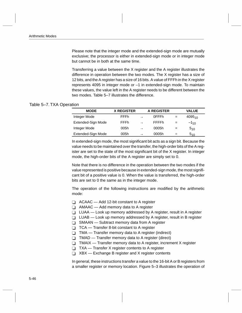
Arithmetic Modes
5-46
Please note that the integer mode and the extended-sign mode are mutuallyexclusive; the processor is either in extended-sign mode or in integer modebut cannot be in both at the same time.
Transferring a value between the X register and the A register illustrates thedifference in operation between the two modes. The X register has a size of12 bits, and the A register has a size of 16 bits. A value of FFFh in the X registerrepresents 4095 in integer mode or –1 in extended-sign mode. To maintainthese values, the value left in the A register needs to be different between thetwo modes. Table 5–7 illustrates the difference.
Table 5–7.TXA OperationMODE X REGISTER A REGISTER VALUE
Integer Mode FFFh → 0FFFh = 409510
Extended-Sign Mode FFFh → FFFFh = –110
Integer Mode 005h → 0005h = 510
Extended-Sign Mode 005h → 0005h = 510
In extended-sign mode, the most significant bit acts as a sign bit. Because thevalue needs to be maintained over the transfer, the high-order bits of the A reg-ister are set to the state of the most significant bit of the X register. In integermode, the high-order bits of the A register are simply set to 0.
Note that there is no difference in the operation between the two modes if thevalue represented is positive because in extended-sign mode, the most signifi-cant bit of a positive value is 0. When the value is transferred, the high-orderbits are set to 0 the same as in the integer mode.
The operation of the following instructions are modified by the arithmeticmode:
ACAAC — Add 12-bit constant to A register AMAAC — Add memory data to A register LUAA — Look up memory addressed by A register, result in A register LUAB — Look up memory addressed by A register, result in B register SMAAN — Subtract memory data from A register TCA — Transfer 8-bit constant to A register TMA — Transfer memory data to A register (indirect) TMAD — Transfer memory data to A register (direct) TMAIX — Transfer memory data to A register, increment X register TXA — Transfer X register contents to A register XBX — Exchange B register and X register contents
In general, these instructions transfer a value to the 16-bit A or B registers froma smaller register or memory location. Figure 5–3 illustrates the operation of
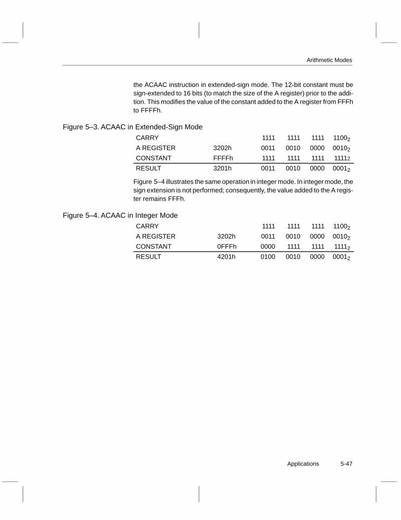
Arithmetic Modes
5-47 Applications
the ACAAC instruction in extended-sign mode. The 12-bit constant must besign-extended to 16 bits (to match the size of the A register) prior to the addi-tion. This modifies the value of the constant added to the A register from FFFhto FFFFh.
Figure 5–3. ACAAC in Extended-Sign Mode
CARRY 1111 1111 1111 11002
A REGISTER 3202h 0011 0010 0000 00102
CONSTANT FFFFh 1111 1111 1111 11112
RESULT 3201h 0011 0010 0000 00012
Figure 5–4 illustrates the same operation in integer mode. In integer mode, thesign extension is not performed; consequently, the value added to the A regis-ter remains FFFh.
Figure 5–4. ACAAC in Integer Mode
CARRY 1111 1111 1111 11002
A REGISTER 3202h 0011 0010 0000 00102
CONSTANT 0FFFh 0000 1111 1111 11112
RESULT 4201h 0100 0010 0000 00012
Operation of the Multiply Instruction
5-48
5.5 Operation of the Multiply Instruction
On digital computers, a multiplication frequently results in a value that is muchlarger than either multiplicand. An example is the multiplication of two 2-bitnumbers:
112 × 112 = 10012
The result of multiplying two 2-bit numbers is a 4-bit number. Similarly, multi-plying the 16-bit A register with the contents of an 8-bit memory location wouldresult in a 24-bit value. This creates a problem because a value this large can-not be stored. One solution would be to limit the size of the multiplicands, butthis would severely restrict the utility of the multiply instruction. A better solu-tion is to interpret the multiplicands as fractions and to truncate the least signifi-cant part of the result. This solution minimizes overflow problems, and trunca-tion affects the least significant portion of the result instead of the most signifi-cant part. In this scheme, an n-bit binary number is interpreted as follows:
value = (–A1 × 20) + (A2 × 2 –1) + . . . + (An × 21 – n),
where A1 . . . An are the bit values of the number. For example, the 4-bit number1010 would be interpreted to have the following value:
value = –1 + (0 × 0.5) + (1 × 0.25) + (0 × 0.125) = – 0.75
Several points need to be emphasized:
The possible values using this scheme range from –1 to slightly lessthan 1.
Since the MSP50C3x instructions are all 8-bit by 16-bit multiply instruc-tions, the lower 8 bits of the result are truncated.
Since the lower 8 bits of the result are truncated, many multiplications givea zero result; for example:
(0000 0000 0000 1111) × (0000 0011) = 0000 0000 0000 0000 | 0010 1101= 0000 0000 0000 0000
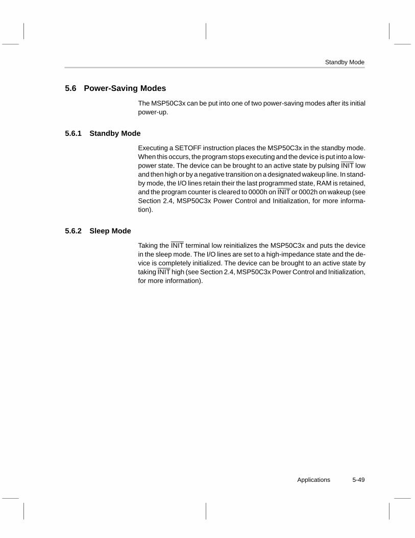
Standby Mode
5-49 Applications
5.6 Power-Saving Modes
The MSP50C3x can be put into one of two power-saving modes after its initialpower-up.
5.6.1 Standby Mode
Executing a SETOFF instruction places the MSP50C3x in the standby mode.When this occurs, the program stops executing and the device is put into a low-power state. The device can be brought to an active state by pulsing INIT lowand then high or by a negative transition on a designated wakeup line. In stand-by mode, the I/O lines retain their the last programmed state, RAM is retained,and the program counter is cleared to 0000h on INIT or 0002h on wakeup (seeSection 2.4, MSP50C3x Power Control and Initialization, for more informa-tion).
5.6.2 Sleep Mode
Taking the INIT terminal low reinitializes the MSP50C3x and puts the devicein the sleep mode. The I/O lines are set to a high-impedance state and the de-vice is completely initialized. The device can be brought to an active state bytaking INIT high (see Section 2.4, MSP50C3x Power Control and Initialization,for more information).
Slave Mode
5-50
5.7 Slave Mode
Setting bit 6 (SLAVE) of mode register 1 to 1 places the MSP50C3x in the slavemode. This specialized mode is intended for applications in which theMSP50C3x device needs to be controlled by a master microprocessor.
When in slave mode, the functionality of the following ports is modified:
B0 becomes a chip enable strobe. It is normally held high. When it is takenlow, data is read from or written to the A0 –A7 ports depending on the stateof B1.
B1 becomes a read/write select input. When B1 is low, data is written tothe MSP50C3x when B0 goes low. When B1 is high, data may be readfrom the MSP50C3x when B0 goes low.
Port A becomes a general bidirectional port controlled by B0 and B1. A7is used as a busy signal. When bit 7 in the output latch is set to 1 by thesoftware, A7 is reset to a low state when B0 goes low to write data to theMSP50C3x.
Because A7 is used as a busy flag, leaving only A0 –A6 for data, normally only7 bits of data may be exchanged between the master and the slave in any oneread operation from the MSP50C3x. In write operations to the MSP50C3x, alleight terminals of port A can transfer data.
During read operations from the slave MSP50C3x, the master is responsiblefor maintaining its outputs connected to the MSP50C3x port A in a high-imped-ance state. Otherwise, bus contention results.
The MSP50C3x I/O ports must be configured in input mode for slave mode towork properly. Port A7 can be put in output mode, if desired. It then functionsas a handshaking line rather than a polled handshake bit.
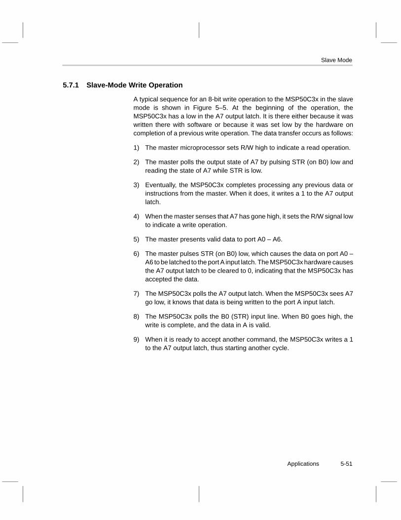
Slave Mode
5-51 Applications
5.7.1 Slave-Mode Write Operation
A typical sequence for an 8-bit write operation to the MSP50C3x in the slavemode is shown in Figure 5–5. At the beginning of the operation, theMSP50C3x has a low in the A7 output latch. It is there either because it waswritten there with software or because it was set low by the hardware oncompletion of a previous write operation. The data transfer occurs as follows:
1) The master microprocessor sets R/W high to indicate a read operation.
2) The master polls the output state of A7 by pulsing STR (on B0) low andreading the state of A7 while STR is low.
3) Eventually, the MSP50C3x completes processing any previous data orinstructions from the master. When it does, it writes a 1 to the A7 outputlatch.
4) When the master senses that A7 has gone high, it sets the R/W signal lowto indicate a write operation.
5) The master presents valid data to port A0 – A6.
6) The master pulses STR (on B0) low, which causes the data on port A0 –A6 to be latched to the port A input latch. The MSP50C3x hardware causesthe A7 output latch to be cleared to 0, indicating that the MSP50C3x hasaccepted the data.
7) The MSP50C3x polls the A7 output latch. When the MSP50C3x sees A7go low, it knows that data is being written to the port A input latch.
8) The MSP50C3x polls the B0 (STR) input line. When B0 goes high, thewrite is complete, and the data in A is valid.
9) When it is ready to accept another command, the MSP50C3x writes a 1to the A7 output latch, thus starting another cycle.
Slave Mode
5-52
Figure 5–5. Slave-Mode Write Operation
(output latch)
B0 (STR)
A7 Busy
B1 (R/W)
Valid Data
Port A(Input Latch)
2 2 6 8
1
3
4
5
2
7
5.7.2 Slave-Mode Read Operation
A typical sequence for an 8-bit read operation from the MSP50C3x in the slavemode is shown in Figure 5–6.
At the beginning of the operation, the MSP50C3x has a low in the A7 outputlatch. It has received a command or a request for information from the master.When the MSP50C3x is ready to respond, the data transfer occurs as follows:
1) The MSP50C3x writes the data to A0 – A6 and a 1 to port A7. The 1 onport A7 is a signal that valid data is available in the terminals connectedto port A.
2) The master periodically polls port A. When it finds A7 has gone high, itknows that A0 – A6 contains valid data.
3) A7 remains high, indicating that the slave is prepared for another com-mand. The master can write to the slave at any time. When the slave pollsthe A7 output latch and finds it low, the slave knows that a new commandfrom the master is in the port A latch.
Slave Mode
5-53 Applications
Figure 5–6. Slave-Mode Read-Then-Write Operation
(output latch)
B0 (STR)
A7 Busy
B1 (R/W)
(output latch)Port A
Data Out
Use of the GET Instruction
5-54
5.8 Use of the GET Instruction
The GET instruction is used to retrieve a bit stream from the RAM or the inter-nal ROM. It allows the program to unpack speech data in a time-efficient man-ner. As shown in Figure 5–7, it is implemented through the use of a parallel-to-serial shift register.
Figure 5–7. Register Connections for GET Instruction
13 12 11 10 9 8 34567 2 1 0
34567 2 1 0
RAM or ROM
34567 2 1 0
Parallel-to-SerialBuffer
A Register
Parallel-to-SerialRegister
The parallel-to-serial register (P/S register) is loaded in a parallel manner fromthe parallel-to-serial buffer (P/S buffer), which is in turn parallel loaded from thesource of the data (which could be internal ROM or internal RAM). When theGET instruction is executed, the number of bits specified in the operand of theGET instruction are shifted out of the LSB of the P/S register into the LSB ofthe A register.
When the number of valid bits in the P/S register is less than the specified num-ber of bits, the contents of the P/S buffer are loaded during operation to the P/Sregister and the contents of the P/S buffer are refreshed from the data sourcethe next time that a GET instruction is executed. The status bit is set to 1. Ifthe buffer did not need to be reloaded, the status bit is cleared to 0.
Note that because the data is shifted out of the LSB of the P/S register and intothe LSB of the A register, there is a byte reflection of the data in this processas illustrated in Figure 5–8. This figure shows the state of the P/S register andthe A register both before and after a GET 5 instruction. Prior to the GET 5,the P/S register contains B716, and the A register contains all zeros. After theinstruction, the least significant 5 bits of the P/S register are shifted into the Aregister. Because of the bit flip, the A register contains 1D16 after the shift op-eration. The P/S register has only 3 valid bits left after the operation. Whenmore than 3 bits are requested in the next GET operation, the P/S register isreloaded from the P/S buffer.
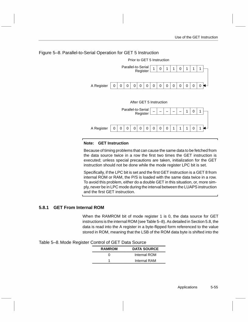
Use of the GET Instruction
5-55 Applications
Figure 5–8. Parallel-to-Serial Operation for GET 5 Instruction
0 0 0 0 0 0 11000 1 0 1
––––– 1 0 1
A Register
Parallel-to-SerialRegister
Prior to GET 5 Instruction
0 0 0 0 0 0 00000 0 0 0
01101 1 1 1
A Register
Parallel-to-SerialRegister
After GET 5 Instruction
Note: GET Instruction
Because of timing problems that can cause the same data to be fetched fromthe data source twice in a row the first two times the GET instruction isexecuted; unless special precautions are taken, initialization for the GETinstruction should not be done while the mode register LPC bit is set.
Specifically, if the LPC bit is set and the first GET instruction is a GET 8 frominternal ROM or RAM, the P/S is loaded with the same data twice in a row.To avoid this problem, either do a double GET in this situation, or, more sim-ply, never be in LPC mode during the interval between the LUAPS instructionand the first GET instruction.
5.8.1 GET From Internal ROM
When the RAMROM bit of mode register 1 is 0, the data source for GETinstructions is the internal ROM (see Table 5–8). As detailed in Section 5.8, thedata is read into the A register in a byte-flipped form referenced to the valuestored in ROM, meaning that the LSB of the ROM data byte is shifted into the
Table 5–8.Mode Register Control of GET Data SourceRAMROM DATA SOURCE
0 Internal ROM
1 Internal RAM
Use of the GET Instruction
5-56
A register first. The recommended sequence for preparing to GET from inter-nal ROM is as follows:
1) Load the starting address of the first desired GET source into theA register.
2) Execute a LUAPS instruction, which performs all required initialization.The processor is now ready to execute a GET instruction starting at theaddress loaded in step 1.
3) When a nonsequential address is desired for a GET, repeat steps 1 and2 for the new address.
When using dual channel synthesis, the speech address register changes asthe channels alternate getting data from ROM. Because of this, the addressalong with the offset must be saved for the next GET on that channel. Thesteps above are extended for dual channels to the following:
4) Load the starting address of the desired GET source into theA register.
5) Execute a LUAPS instruction.
6) Load the offset of the address into the A register.
7) Execute a GET instruction. This adjusts the P/S buffer when needed. Theprocessor is now ready to execute a GET instruction starting at the ad-dress + bit offset.
5.8.2 GET From Internal RAM
When the RAMROM bit is set in mode register 1, the data source for GETinstructions is the internal RAM. As detailed in Section 5.8, the data is read intothe A register in a byte-flipped form from the value stored in RAM, meaning thatthe LSB of the RAM data byte is shifted into the A register first.
The usage of the GET instruction while in RAM mode is somewhat more com-plicated than when the data source is from ROM because the burden of provid-ing the address used to refresh the P/S buffer falls on the software.
When a GET instruction exhausts the P/S register, the value stored in the P/Sbuffer is loaded into the P/S register, and the GET instruction returns with thestatus set. When the next GET instruction is executed, the P/S buffer is loadedwith the value stored in the RAM location pointed to by the X register.
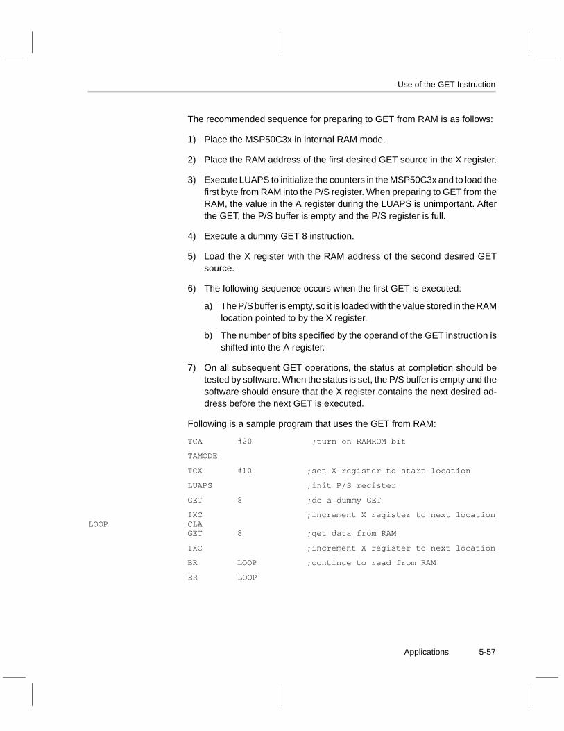
Use of the GET Instruction
5-57 Applications
The recommended sequence for preparing to GET from RAM is as follows:
1) Place the MSP50C3x in internal RAM mode.
2) Place the RAM address of the first desired GET source in the X register.
3) Execute LUAPS to initialize the counters in the MSP50C3x and to load thefirst byte from RAM into the P/S register. When preparing to GET from theRAM, the value in the A register during the LUAPS is unimportant. Afterthe GET, the P/S buffer is empty and the P/S register is full.
4) Execute a dummy GET 8 instruction.
5) Load the X register with the RAM address of the second desired GETsource.
6) The following sequence occurs when the first GET is executed:
a) The P/S buffer is empty, so it is loaded with the value stored in the RAMlocation pointed to by the X register.
b) The number of bits specified by the operand of the GET instruction isshifted into the A register.
7) On all subsequent GET operations, the status at completion should betested by software. When the status is set, the P/S buffer is empty and thesoftware should ensure that the X register contains the next desired ad-dress before the next GET is executed.
Following is a sample program that uses the GET from RAM:
TCA #20 ;turn on RAMROM bit
TAMODE
TCX #10 ;set X register to start location
LUAPS ;init P/S register
GET 8 ;do a dummy GET
IXC ;increment X register to next locationLOOP CLA GET 8 ;get data from RAM
IXC ;increment X register to next location
BR LOOP ;continue to read from RAM
BR LOOP
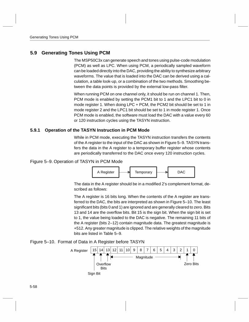
Generating Tones Using PCM
5-58
5.9 Generating Tones Using PCMThe MSP50C3x can generate speech and tones using pulse-code modulation(PCM) as well as LPC. When using PCM, a periodically sampled waveformcan be loaded directly into the DAC, providing the ability to synthesize arbitrarywaveforms. The value that is loaded into the DAC can be derived using a cal-culation, a table look-up, or a combination of the two methods. Smoothing be-tween the data points is provided by the external low-pass filter.
When running PCM on one channel only, it should be run on channel 1. Then,PCM mode is enabled by setting the PCM1 bit to 1 and the LPC1 bit to 0 inmode register 1. When doing LPC + PCM, the PCM2 bit should be set to 1 inmode register 2 and the LPC1 bit should be set to 1 in mode register 1. OncePCM mode is enabled, the software must load the DAC with a value every 60or 120 instruction cycles using the TASYN instruction.
5.9.1 Operation of the TASYN Instruction in PCM Mode
While in PCM mode, executing the TASYN instruction transfers the contentsof the A register to the input of the DAC as shown in Figure 5–9. TASYN trans-fers the data in the A register to a temporary buffer register whose contentsare periodically transferred to the DAC once every 120 instruction cycles.
Figure 5–9. Operation of TASYN in PCM Mode
A Register Temporary DAC
The data in the A register should be in a modified 2’s complement format, de-scribed as follows:
The A register is 16 bits long. When the contents of the A register are trans-ferred to the DAC, the bits are interpreted as shown in Figure 5–10. The leastsignificant bits (bits 0 and 1) are ignored and are generally cleared to zero. Bits13 and 14 are the overflow bits. Bit 15 is the sign bit. When the sign bit is setto 1, the value being loaded to the DAC is negative. The remaining 11 bits ofthe A register (bits 2–12) contain magnitude data. The greatest magnitude is+512. Any greater magnitude is clipped. The relative weights of the magnitudebits are listed in Table 5–9.
Figure 5–10. Format of Data in A Register before TASYN
13 12 11 10 9 8 34567 2 1 0A Register
Magnitude
OverflowBits
Zero Bits
15 14
Sign Bit
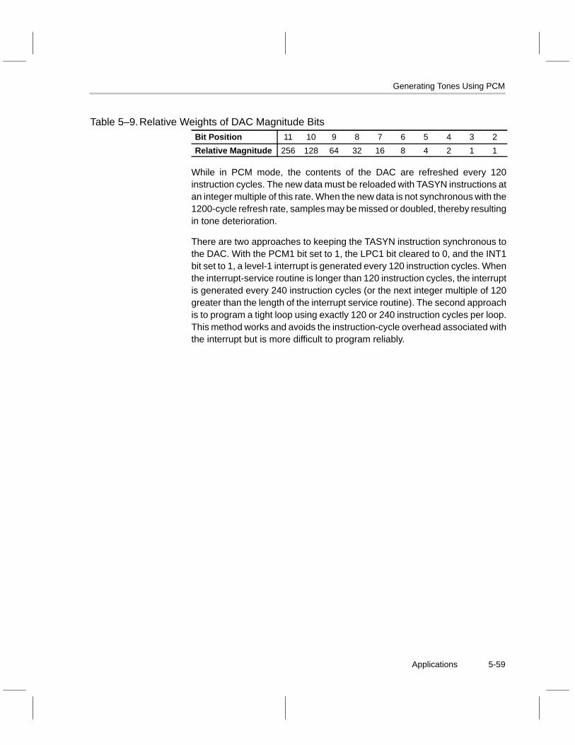
Generating Tones Using PCM
5-59 Applications
Table 5–9.Relative Weights of DAC Magnitude BitsBit Position 11 10 9 8 7 6 5 4 3 2
Relative Magnitude 256 128 64 32 16 8 4 2 1 1
While in PCM mode, the contents of the DAC are refreshed every 120instruction cycles. The new data must be reloaded with TASYN instructions atan integer multiple of this rate. When the new data is not synchronous with the1200-cycle refresh rate, samples may be missed or doubled, thereby resultingin tone deterioration.
There are two approaches to keeping the TASYN instruction synchronous tothe DAC. With the PCM1 bit set to 1, the LPC1 bit cleared to 0, and the INT1bit set to 1, a level-1 interrupt is generated every 120 instruction cycles. Whenthe interrupt-service routine is longer than 120 instruction cycles, the interruptis generated every 240 instruction cycles (or the next integer multiple of 120greater than the length of the interrupt service routine). The second approachis to program a tight loop using exactly 120 or 240 instruction cycles per loop.This method works and avoids the instruction-cycle overhead associated withthe interrupt but is more difficult to program reliably.
PCM + LPC
5-60
5.10 PCM + LPC
The MSP50C3x can also generate speech and tones using PCM + LPC. Toaccomplish this, the LPC must be run on channel 1 and the PCM must be onchannel 2.
A simple way to do PCM + LPC is to use the standard single channel LPC rou-tine (found in Appendix D) and add to it the PCM interrupt routine and the ap-propriate initializations. The PCM interrupt routine controls the sample rate.PCM + LPC mode can be enabled by setting the LPC1 bit (for channel 1) to1, the ENA1 bit to 1, and the PCM2 bit (for channel 2) to 1. One thing to remem-ber, as with dual LPC, the channel bit must be set or cleared to select the ap-propriate channel before the TASYN instruction is given.
6-1
Customer Information
Customer information on development cycle organization, development andproduction sequence, mechanical information and packaging availability,ordering information, and example ordering forms are all included in thischapter.
Topic Page
6.1 Development Cycle 6-2. . . . . . . . . . . . . . . . . . . . . . . . . . . . . . . . . . . . . . . . . . .
6.2 Summary of Speech Development/Production Sequence 6-3. . . . . . . . .
6.3 Mechanical Information 6-4. . . . . . . . . . . . . . . . . . . . . . . . . . . . . . . . . . . . . . . .
6.4 Ordering Information 6-10. . . . . . . . . . . . . . . . . . . . . . . . . . . . . . . . . . . . . . . . .
6.5 New Product Release Forms (MSP50C3x) 6-11. . . . . . . . . . . . . . . . . . . . . .
Chapter 6
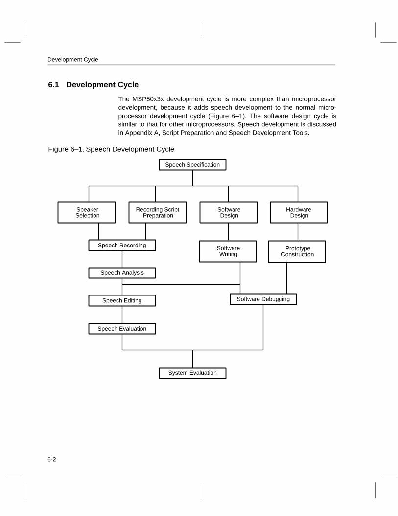
Development Cycle
6-2
6.1 Development Cycle
The MSP50x3x development cycle is more complex than microprocessordevelopment, because it adds speech development to the normal micro-processor development cycle (Figure 6–1). The software design cycle issimilar to that for other microprocessors. Speech development is discussedin Appendix A, Script Preparation and Speech Development Tools.
Figure 6–1. Speech Development Cycle
Speech Specification
Speech Recording
Speech Analysis
Speech Editing
Speech Evaluation
Software Debugging
System Evaluation
PrototypeConstruction
Recording ScriptPreparation
SpeakerSelection
SoftwareDesign
HardwareDesign
SoftwareWriting
Summary of Speech Development/Production Sequence
6-3 Customer Information
6.2 Summary of Speech Development/Production Sequence
The following is a summary of the speech development /production sequence:
1) For the Speech Development Group at TI to accept a custom device pro-gram, the customer must submit a new product release form (NPRF). Thisform describes the custom features of the device (e.g., customer informa-tion, prototype and production qualities, symbolization, etc.). Copies ofblank NPRF forms can be found in subsections of 6.5.
2) TI generates the prototype photomask and processes, manufactures, andtests 25 packaged or 196 die initial prototype devices for shipment to thecustomer. Limited quantities of prototype devices in addition to the initialprototypes can be purchased for use in customer evaluation. All prototypedevices are shipped against the following disclaimer: “It is understoodthat, for expediency purposes, the initial prototype devices (and any addi-tional prototype devices purchased) were assembled on a prototype (i.e.,not production-qualified) manufacturing line whose reliability has not beencharacterized. Therefore, the anticipated inherent reliability of these de-vices cannot be expressly defined.”
3) The customer verifies the operation and quality of these prototypes andresponds with either written customer prototype approval or disapproval.
4) A nonrecurring mask charge that includes the initial prototype devices isincurred by the customer.
5) A minimum purchase may be required during the first year of production.
Note: Using Prototype Devices in Production Systems
Texas Instruments recommends that prototype devices not be used in pro-duction systems because their expected end-use failure rate is undefinedbut is predicted to be greater than standard qualified production.
Mechanical Information
6-4
6.3 Mechanical Information
Most of the MSP50C3x family is available in either a 16-pin plastic small-out-line wide-body (SOWB) DW package, a 16-pin plastic dual-in-line N package(DIP), or in die form. The MSP50P34 is also available in a 40-pin plastic DIPNW package. The MSP50C37 is available in a 28-pin small-outline wide-body(SOWB) DW package or a 28-pin plastic dual-in-line N package (DIP).
6.3.1 N and NW Plastic Dual-In-Line Packages
N (Figure 6–2) 16-pin plastic DIP packages of the MSP50C32/33/34, N (Figure6–3) 28-pin plastic DIP packages of the MSP50x37, and the NW040 40-pinplastic DIP package of the MSP50P34 (Figure 6–4) consist of a circuitmounted in a lead frame and encapsulated within an electrically nonconduc-tive plastic compound. The compound withstands soldering temperature withno deformation, and circuit performance characteristics remain stable whenoperated in high-humidity conditions. Once the leads are compressed and in-serted, sufficient tension is provided to secure the package in the board duringsoldering. Leads require no additional cleaning or processing when used in thesoldered assembly.
Mechanical Information
6-5 Customer Information
Figure 6–2. MSP50C32/33/34 16-Pin N PackageN (R-PDIP-T**) PLASTIC DUAL-IN-LINE PACKAGE
20
0.975(24,77)
0.940(23,88)
18
0.920
0.850
14
0.775
0.745
(19,69)
(18,92)
16
0.775(19,69)
(18,92)0.745
A MIN
DIM
A MAX
PINS **
0.310 (7,87)0.290 (7,37)
(23.37)
(21.59)
Seating Plane
0.010 (0,25) NOM
14/18 PIN ONLY
4040049/C 08/95
9
8
0.070 (1,78) MAX
A
0.035 (0,89) MAX 0.020 (0,51) MIN
16
1
0.015 (0,38)0.021 (0,53)
0.200 (5,08) MAX
0.125 (3,18) MIN
0.240 (6,10)0.260 (6,60)
M0.010 (0,25)
0.100 (2,54)0°–15°
16 PIN SHOWN
NOTES: A. All linear dimensions are in inches (millimeters).B. This drawing is subject to change without notice.C. Falls within JEDEC MS-001 (20 pin package is shorter then MS-001.)
Mechanical Information
6-6
Figure 6–3. MSP50x37 28-Pin N PackageN (R-PDIP-T**) PLASTIC DUAL-IN-LINE PACKAGE24 PIN SHOWN
12
Seating Plane
0.560 (14,22)0.520 (13,21)
13
0.610 (15,49)0.590 (14,99)
524840
0.125 (3,18) MIN
2.390(60,71)
(62,23)(53,09)
(51,82)2.040
2.090 2.450 2.650(67,31)
(65,79)2.590
0.010 (0,25) NOM
4040053/B 04/95
A
0.060 (1,52) TYP
1
24
322824
1.230(31,24)
(32,26) (36,83)
(35,81)1.410
1.4501.270
PINS **DIM
0.015 (0,38)0.021 (0,53)
A MIN
A MAX1.650
(41,91)
(40,89)1.610
0.020 (0,51) MIN
0.200 (5,08) MAX
0.100 (2,54)
M0.010(0,25)
0°–15°
NOTES: A. All linear dimensions are in inches (millimeters).B. This drawing is subject to change without notice.C. Falls within JEDEC MS-011D. Falls within JEDEC MS-015 (32 pin only)
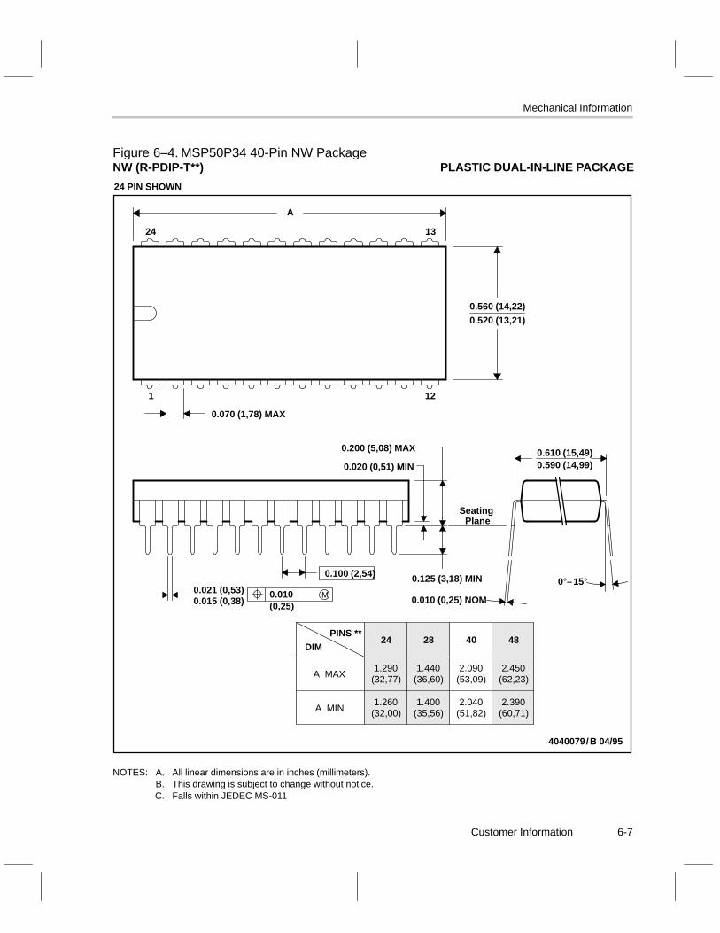
Mechanical Information
6-7 Customer Information
Figure 6–4. MSP50P34 40-Pin NW PackageNW (R-PDIP-T**) PLASTIC DUAL-IN-LINE PACKAGE
24 PIN SHOWN
4040079/B 04/95
0.560 (14,22)0.520 (13,21)
12
Seating Plane
13
0.610 (15,49)0.590 (14,99)
4828 40
0.125 (3,18) MIN
2.390(60,71)
(62,23)
1.400 2.040(51,82)
(53,09)1.440 2.090 2.450
0.010 (0,25) NOM
A
0.070 (1,78) MAX
1
24
24DIM
PINS **
(32,77)
(32,00)1.260
A MAX
A MIN
1.290
0.021 (0,53)0.015 (0,38)
(35,56)
(36,60)
0.020 (0,51) MIN
0.200 (5,08) MAX
0.100 (2,54)
M0.010(0,25)
0°–15°
NOTES: A. All linear dimensions are in inches (millimeters).B. This drawing is subject to change without notice.C. Falls within JEDEC MS-011
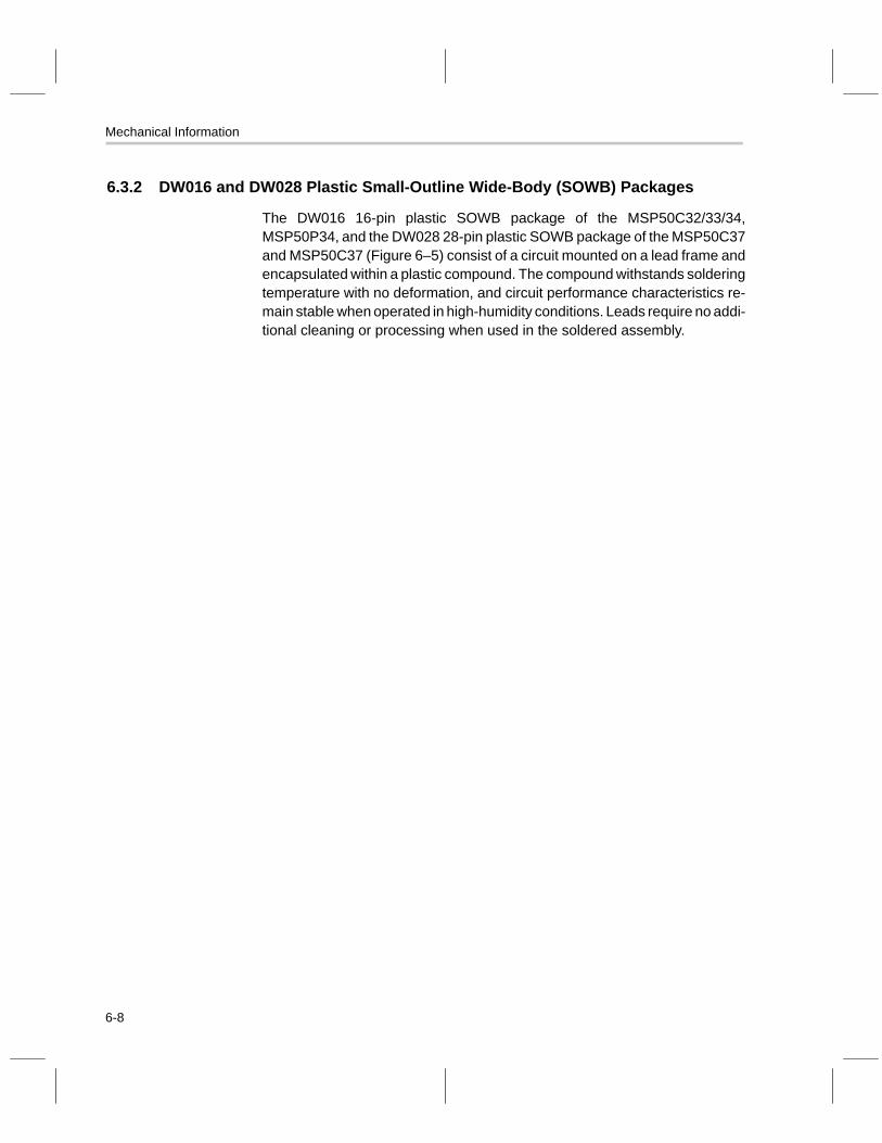
Mechanical Information
6-8
6.3.2 DW016 and DW028 Plastic Small-Outline Wide-Body (SOWB) Packages
The DW016 16-pin plastic SOWB package of the MSP50C32/33/34,MSP50P34, and the DW028 28-pin plastic SOWB package of the MSP50C37and MSP50C37 (Figure 6–5) consist of a circuit mounted on a lead frame andencapsulated within a plastic compound. The compound withstands solderingtemperature with no deformation, and circuit performance characteristics re-main stable when operated in high-humidity conditions. Leads require no addi-tional cleaning or processing when used in the soldered assembly.
Mechanical Information
6-9 Customer Information
Figure 6–5. MSP50C32/33/34/37 and MSP50P34/37 DW PackageDW (R-PDSO-G**) PLASTIC SMALL-OUTLINE PACKAGE16 PIN SHOWN
4040000/B 03/95
Seating Plane
0.400 (10,15)0.419 (10,65)
0.104 (2,65) MAX
1
0.012 (0,30)0.004 (0,10)
A
8
16
0.020 (0,51)0.014 (0,35)
0.293 (7,45)0.299 (7,59)
9
0.010 (0,25)
0.050 (1,27)0.016 (0,40)
(15,24)
(15,49)
PINS **
0.010 (0,25) NOM
A MAX
DIM
A MIN
Gage Plane
20
0.500(12,70)
(12,95)0.510
(10,16)
(10,41)
0.400
0.410
16
0.600
24
0.610
(17,78)
28
0.700
(18,03)0.710
0.004 (0,10)
M0.010 (0,25)
0.050 (1,27)
0°–8°
NOTES: A. All linear dimensions are in inches (millimeters).B. This drawing is subject to change without notice.C. Body dimensions do not include mold flash or protrusion not to exceed 0.006 (0,15).D. Falls within JEDEC MS-013
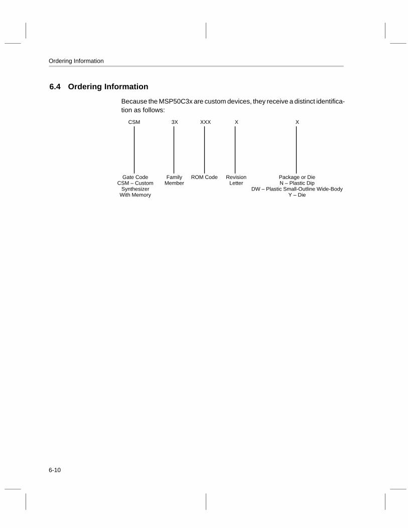
Ordering Information
6-10
6.4 Ordering Information
Because the MSP50C3x are custom devices, they receive a distinct identifica-tion as follows:
CSM
Gate CodeCSM – Custom
SynthesizerWith Memory
XXX
ROM Code
X
RevisionLetter
X
Package or DieN – Plastic Dip
DW – Plastic Small-Outline Wide-BodyY – Die
3X
FamilyMember
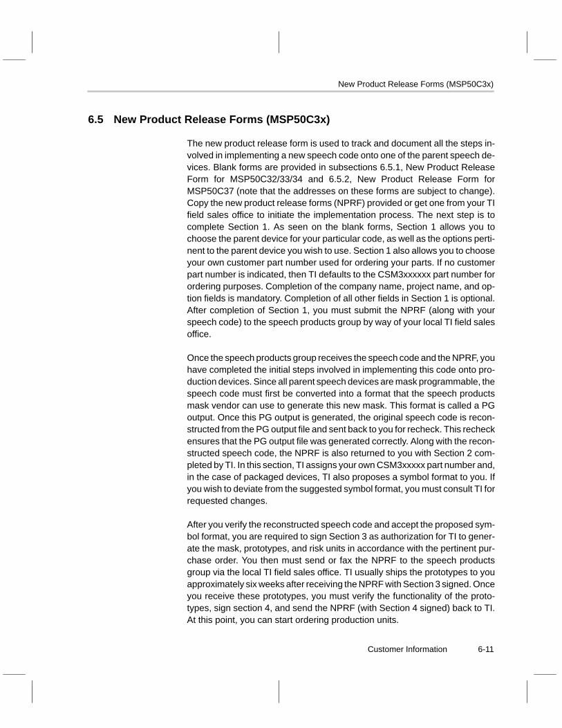
New Product Release Forms (MSP50C3x)
6-11 Customer Information
6.5 New Product Release Forms (MSP50C3x)
The new product release form is used to track and document all the steps in-volved in implementing a new speech code onto one of the parent speech de-vices. Blank forms are provided in subsections 6.5.1, New Product ReleaseForm for MSP50C32/33/34 and 6.5.2, New Product Release Form forMSP50C37 (note that the addresses on these forms are subject to change).Copy the new product release forms (NPRF) provided or get one from your TIfield sales office to initiate the implementation process. The next step is tocomplete Section 1. As seen on the blank forms, Section 1 allows you tochoose the parent device for your particular code, as well as the options perti-nent to the parent device you wish to use. Section 1 also allows you to chooseyour own customer part number used for ordering your parts. If no customerpart number is indicated, then TI defaults to the CSM3xxxxxx part number forordering purposes. Completion of the company name, project name, and op-tion fields is mandatory. Completion of all other fields in Section 1 is optional.After completion of Section 1, you must submit the NPRF (along with yourspeech code) to the speech products group by way of your local TI field salesoffice.
Once the speech products group receives the speech code and the NPRF, youhave completed the initial steps involved in implementing this code onto pro-duction devices. Since all parent speech devices are mask programmable, thespeech code must first be converted into a format that the speech productsmask vendor can use to generate this new mask. This format is called a PGoutput. Once this PG output is generated, the original speech code is recon-structed from the PG output file and sent back to you for recheck. This recheckensures that the PG output file was generated correctly. Along with the recon-structed speech code, the NPRF is also returned to you with Section 2 com-pleted by TI. In this section, TI assigns your own CSM3xxxxx part number and,in the case of packaged devices, TI also proposes a symbol format to you. Ifyou wish to deviate from the suggested symbol format, you must consult TI forrequested changes.
After you verify the reconstructed speech code and accept the proposed sym-bol format, you are required to sign Section 3 as authorization for TI to gener-ate the mask, prototypes, and risk units in accordance with the pertinent pur-chase order. You then must send or fax the NPRF to the speech productsgroup via the local TI field sales office. TI usually ships the prototypes to youapproximately six weeks after receiving the NPRF with Section 3 signed. Onceyou receive these prototypes, you must verify the functionality of the proto-types, sign section 4, and send the NPRF (with Section 4 signed) back to TI.At this point, you can start ordering production units.

New Product Release Forms (MSP50C3x)
6-12
6.5.1 New Product Release Form for MSP50C32
NEW PRODUCT RELEASE FORM FOR MSP50C32
SECTION 1. OPTION SELECTION This section is to be completed by the customer and sent to TI along with the microprocessor code and speech data.
Company:_____________________________ Division:_____________________________Project Name:________________________ Purchase Order #:_____________________Management Contact: _______________________________ Phone:(___) _____________Technical Contact : _______________________________ Phone:(___) _____________Customer Part Number:_____________________________
D/A Output (check one):
___ 2 pin push-pull (2D)
___ Single pin double ended (1A)
Oscillator (check one):
___ Internal (Two ranges selected by software: 1) 15.36 MHz (14.89 MHz – 15.82 MHz) 2) 19.2 MHz (18.62 MHz – 19.77 MHz))
___ External
Package Type (check one):
___ N (16 pin)
___ SOWB (16 pin) ___ Tube ___ Reel
___ Die
******************************************************************************
SECTION 2A. ASSIGNMENT OF TI PRODUCTION PART NUMBER This section is to be completed by TI.
TI Part Number:______________
SECTION 2B. ASSIGNMENT OF SYMBOLIZATION FORMAT The section is to be completed by the customer. The first line of the symbolization is fixed. Except EIA#/Logo. The second and third lines are to be filled in by the customer.
Top Side Symbolization (16 pin ’N’) +–––––––––––––––––––––––+ LLLL: LOT TRACE CODE | ??? YMLLLLT | YM: DATE CODE | <optional 13 char> | T: ASSY SITE | <optional 11 char> | ???: TI EIA NO. or +–––––––––––––––––––––––+ TI LOGO
For ’16N’ package, the customer may choose between 980 or the TI LOGO on the firstline.
Top Side Symbolization (16 pin ’SOWB’) +–––––––––––––––––––––––+ LLLL: LOT TRACE CODE | \T/ YMLLLLT | YM: DATE CODE | <optional 9 char> | T: ASSY SITE | <optional 6 char> | \T/: TI LOGO +–––––––––––––––––––––––+
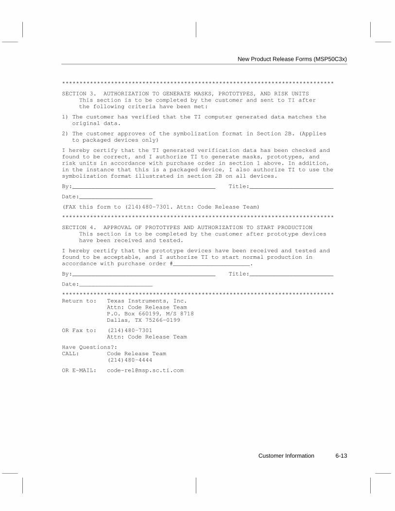
New Product Release Forms (MSP50C3x)
6-13 Customer Information
******************************************************************************
SECTION 3. AUTHORIZATION TO GENERATE MASKS, PROTOTYPES, AND RISK UNITS This section is to be completed by the customer and sent to TI after the following criteria have been met:
1) The customer has verified that the TI computer generated data matches the original data.
2) The customer approves of the symbolization format in Section 2B. (Applies to packaged devices only)
I hereby certify that the TI generated verification data has been checked andfound to be correct, and I authorize TI to generate masks, prototypes, andrisk units in accordance with purchase order in section 1 above. In addition,in the instance that this is a packaged device, I also authorize TI to use thesymbolization format illustrated in section 2B on all devices.
By:_________________________________________ Title:________________________
Date:_____________________
(FAX this form to (214)480–7301. Attn: Code Release Team)
******************************************************************************
SECTION 4. APPROVAL OF PROTOTYPES AND AUTHORIZATION TO START PRODUCTION This section is to be completed by the customer after prototype devices have been received and tested.
I hereby certify that the prototype devices have been received and tested andfound to be acceptable, and I authorize TI to start normal production inaccordance with purchase order #______________________.
By:_________________________________________ Title:________________________
Date:_____________________
******************************************************************************Return to: Texas Instruments, Inc. Attn: Code Release Team P.O. Box 660199, M/S 8718 Dallas, TX 75266–0199
OR Fax to: (214)480–7301 Attn: Code Release Team
Have Questions?:CALL: Code Release Team (214)480–4444
OR E–MAIL: code–[email protected]
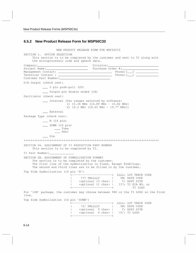
New Product Release Forms (MSP50C3x)
6-14
6.5.2 New Product Release Form for MSP50C33
NEW PRODUCT RELEASE FORM FOR MSP50C33
SECTION 1. OPTION SELECTION This section is to be completed by the customer and sent to TI along with the microprocessor code and speech data.
Company:_____________________________ Division:_____________________________Project Name:________________________ Purchase Order #:_____________________Management Contact: _______________________________ Phone:(___) _____________Technical Contact : _______________________________ Phone:(___) _____________Customer Part Number:_____________________________
D/A Output (check one):
___ 2 pin push-pull (2D)
___ Single pin double ended (1A)
Oscillator (check one):
___ Internal (Two ranges selected by software: 1) 15.36 MHz (14.89 MHz – 15.82 MHz) 2) 19.2 MHz (18.62 MHz – 19.77 MHz))
___ External
Package Type (check one):
___ N (16 pin)
___ SOWB (16 pin) ___ Tube ___ Reel
___ Die
******************************************************************************
SECTION 2A. ASSIGNMENT OF TI PRODUCTION PART NUMBER This section is to be completed by TI.
TI Part Number:______________
SECTION 2B. ASSIGNMENT OF SYMBOLIZATION FORMAT The section is to be completed by the customer. The first line of the symbolization is fixed. Except EIA#/Logo. The second and third lines are to be filled in by the customer.
Top Side Symbolization (16 pin ’N’) +–––––––––––––––––––––––+ LLLL: LOT TRACE CODE | ??? YMLLLLT | YM: DATE CODE | <optional 13 char> | T: ASSY SITE | <optional 11 char> | ???: TI EIA NO. or +–––––––––––––––––––––––+ TI LOGO
For ’16N’ package, the customer may choose between 980 or the TI LOGO on the firstline.
Top Side Symbolization (16 pin ’SOWB’) +–––––––––––––––––––––––+ LLLL: LOT TRACE CODE | \T/ YMLLLLT | YM: DATE CODE | <optional 9 char> | T: ASSY SITE | <optional 6 char> | \T/: TI LOGO +–––––––––––––––––––––––+

New Product Release Forms (MSP50C3x)
6-15 Customer Information
******************************************************************************
SECTION 3. AUTHORIZATION TO GENERATE MASKS, PROTOTYPES, AND RISK UNITS This section is to be completed by the customer and sent to TI after the following criteria have been met:
1) The customer has verified that the TI computer generated data matches the original data.
2) The customer approves of the symbolization format in Section 2B. (Applies to packaged devices only)
I hereby certify that the TI generated verification data has been checked andfound to be correct, and I authorize TI to generate masks, prototypes, andrisk units in accordance with purchase order in section 1 above. In addition,in the instance that this is a packaged device, I also authorize TI to use thesymbolization format illustrated in section 2B on all devices.
By:_________________________________________ Title:________________________
Date:_____________________
(FAX this form to (214)480–7301. Attn: Code Release Team)
******************************************************************************
SECTION 4. APPROVAL OF PROTOTYPES AND AUTHORIZATION TO START PRODUCTION This section is to be completed by the customer after prototype devices have been received and tested.
I hereby certify that the prototype devices have been received and tested andfound to be acceptable, and I authorize TI to start normal production inaccordance with purchase order #______________________.
By:_________________________________________ Title:________________________
Date:_____________________
******************************************************************************Return to: Texas Instruments, Inc. Attn: Code Release Team P.O. Box 660199, M/S 8718 Dallas, TX 75266–0199
OR Fax to: (214)480–7301 Attn: Code Release Team
Have Questions?:CALL: Code Release Team (214)480–4444
OR E–MAIL: code–[email protected]

New Product Release Forms (MSP50C3x)
6-16
6.5.3 New Product Release Form for MSP50C34
NEW PRODUCT RELEASE FORM FOR MSP50C34
SECTION 1. OPTION SELECTION This section is to be completed by the customer and sent to TI along with the microprocessor code and speech data.
Company:_____________________________ Division:_____________________________Project Name:________________________ Purchase Order #:_____________________Management Contact: _______________________________ Phone:(___) _____________Technical Contact : _______________________________ Phone:(___) _____________Customer Part Number:_____________________________
D/A Output (check one):
___ 2 pin push–pull (2D)
___ Single pin double ended (1A)
Oscillator (check one):
___ Internal (Two ranges selected by software: 1) 15.36MHz (14.89MHz – 15.82MHz) 2) 19.2MHz (18.62MHz – 19.77MHz))
___ External
Package Type (check one):
___ N (16 pin)
___ SOWB (16 pin) ___ Tube ___ Reel
___ Die Number of I/O (Die Sales Only) ___ 10 ___ 24
******************************************************************************
SECTION 2A. ASSIGNMENT OF TI PRODUCTION PART NUMBER This section is to be completed by TI.
TI Part Number:______________
SECTION 2B. ASSIGNMENT OF SYMBOLIZATION FORMAT The section is to be completed by the customer. The first line of the symbolization is fixed. Except EIA#/Logo. The second and third lines are to be filled in by the customer.
Top Side Symbolization (16 pin ’N’) +–––––––––––––––––––––––+ LLLL: LOT TRACE CODE | ??? YMLLLLT | YM: DATE CODE | <optional 13 char> | T: ASSY SITE | <optional 11 char> | ???: TI EIA NO. or +–––––––––––––––––––––––+ TI LOGO
For ’16N’ package, the customer may choose between 980 or the TI LOGO on the firstline.

New Product Release Forms (MSP50C3x)
6-17 Customer Information
Top Side Symbolization (16 pin ’SOWB’) +–––––––––––––––––––––––+ LLLL: LOT TRACE CODE | \T/ YMLLLLT | YM: DATE CODE | <optional 9 char> | T: ASSY SITE | <optional 6 char> | \T/: TI LOGO +–––––––––––––––––––––––+
******************************************************************************
SECTION 3. AUTHORIZATION TO GENERATE MASKS, PROTOTYPES, AND RISK UNITS This section is to be completed by the customer and sent to TI after the following criteria have been met:
1) The customer has verified that the TI computer generated data matches the original data.
2) The customer approves of the symbolization format in Section 2B. (Applies to packaged devices only)
I hereby certify that the TI generated verification data has been checked andfound to be correct, and I authorize TI to generate masks, prototypes, andrisk units in accordance with purchase order in section 1 above. In addition,in the instance that this is a packaged device, I also authorize TI to use thesymbolization format illustrated in section 2B on all devices.
By:_________________________________________ Title:________________________
Date:_____________________
(FAX this form to (214)480–7301. Attn: Code Release Team)
******************************************************************************
SECTION 4. APPROVAL OF PROTOTYPES AND AUTHORIZATION TO START PRODUCTION This section is to be completed by the customer after prototype devices have been received and tested.
I hereby certify that the prototype devices have been received and tested andfound to be acceptable, and I authorize TI to start normal production inaccordance with purchase order #______________________.
By:_________________________________________ Title:________________________
Date:_____________________
******************************************************************************Return to: Texas Instruments, Inc. Attn: Code Release Team P.O. Box 660199, M/S 8718 Dallas, TX 75266–0199
OR Fax to: (214)480–7301 Attn: Code Release Team
Have Questions?:CALL: Code Release Team (214)480–4444
OR E–MAIL: code–[email protected]
New Product Release Forms (MSP50C3x)
6-18
6.5.4 New Product Release Form for MSP50C37
NEW PRODUCT RELEASE FORM FOR MSP50C37
SECTION 1. OPTION SELECTION This section is to be completed by the customer and sent to TI along with the microprocessor code and speech data.
Company:_____________________________ Division:_____________________________Project Name:________________________ Purchase Order #:_____________________Management Contact: _______________________________ Phone:(___) _____________Technical Contact : _______________________________ Phone:(___) _____________Customer Part Number:_____________________________
POWER AMP (CHECK ONE) ___ DUAL OUTPUT ___ SINGLE OUTPUT
Package Type (check one): ___ N (28 pin) ___ SOWB (28 pin) ___ Tube ___ Reel
******************************************************************************SECTION 2A. ASSIGNMENT OF TI PRODUCTION PART NUMBER This section is to be completed by TI.
TI Part Number:______________
SECTION 2B. ASSIGNMENT OF SYMBOLIZATION FORMAT The section is to be completed by the customer. The first line of the symbolization is fixed. The second and third lines are to be filled in by the customer.
Top Side Symbolization (28 pin ’N’) +–––––––––––––––––––––––+ LLLL: LOT TRACE CODE | ??? YMLLLLT | YM: DATE CODE | <optional 13 char> | T: ASSY SITE | <optional 11 char> | ???: TI EIA NO. or +–––––––––––––––––––––––+ TI LOGO
For ’28N’ package, the customer may choose between 980 or the TI LOGO on the firstline.
Top Side Symbolization (28 pin ’SOWB’) +–––––––––––––––––––––––+ LLLL: LOT TRACE CODE | \T/ YMLLLLT | YM: DATE CODE | <optional 10 char> | T: ASSY SITE | <optional 6 char> | \T/: TI LOGO +–––––––––––––––––––––––+
******************************************************************************
SECTION 3. AUTHORIZATION TO GENERATE MASKS, PROTOTYPES, AND RISK UNITS This section is to be completed by the customer and sent to TI after the following criteria have been met:
1) The customer has verified that the TI computer generated data matches the original data.
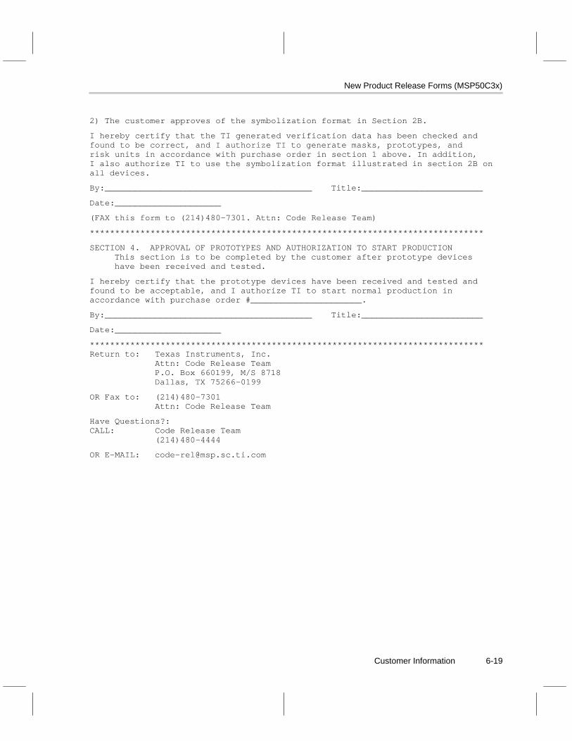
New Product Release Forms (MSP50C3x)
6-19 Customer Information
2) The customer approves of the symbolization format in Section 2B.
I hereby certify that the TI generated verification data has been checked andfound to be correct, and I authorize TI to generate masks, prototypes, andrisk units in accordance with purchase order in section 1 above. In addition,I also authorize TI to use the symbolization format illustrated in section 2B onall devices.
By:_________________________________________ Title:________________________
Date:_____________________
(FAX this form to (214)480–7301. Attn: Code Release Team)
******************************************************************************
SECTION 4. APPROVAL OF PROTOTYPES AND AUTHORIZATION TO START PRODUCTION This section is to be completed by the customer after prototype devices have been received and tested.
I hereby certify that the prototype devices have been received and tested andfound to be acceptable, and I authorize TI to start normal production inaccordance with purchase order #______________________.
By:_________________________________________ Title:________________________
Date:_____________________
******************************************************************************Return to: Texas Instruments, Inc. Attn: Code Release Team P.O. Box 660199, M/S 8718 Dallas, TX 75266–0199
OR Fax to: (214)480–7301 Attn: Code Release Team
Have Questions?:CALL: Code Release Team (214)480–4444
OR E–MAIL: code–[email protected]
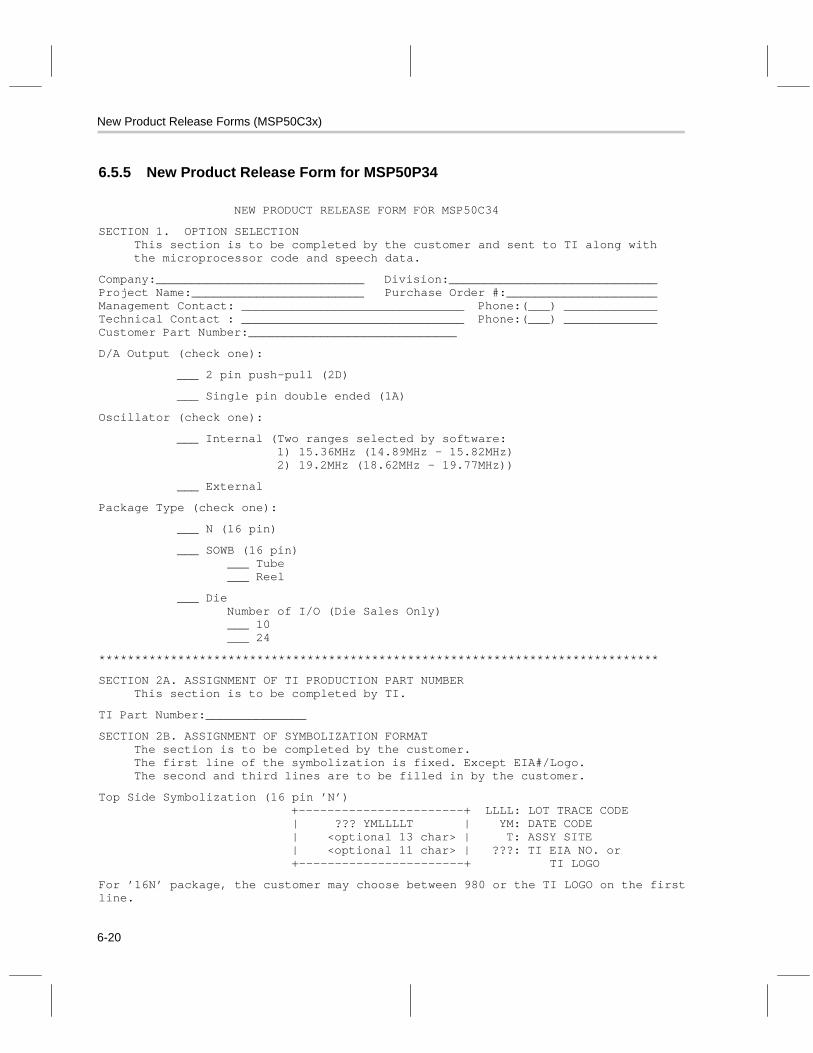
New Product Release Forms (MSP50C3x)
6-20
6.5.5 New Product Release Form for MSP50P34
NEW PRODUCT RELEASE FORM FOR MSP50C34
SECTION 1. OPTION SELECTION This section is to be completed by the customer and sent to TI along with the microprocessor code and speech data.
Company:_____________________________ Division:_____________________________Project Name:________________________ Purchase Order #:_____________________Management Contact: _______________________________ Phone:(___) _____________Technical Contact : _______________________________ Phone:(___) _____________Customer Part Number:_____________________________
D/A Output (check one):
___ 2 pin push–pull (2D)
___ Single pin double ended (1A)
Oscillator (check one):
___ Internal (Two ranges selected by software: 1) 15.36MHz (14.89MHz – 15.82MHz) 2) 19.2MHz (18.62MHz – 19.77MHz))
___ External
Package Type (check one):
___ N (16 pin)
___ SOWB (16 pin) ___ Tube ___ Reel
___ Die Number of I/O (Die Sales Only) ___ 10 ___ 24
******************************************************************************
SECTION 2A. ASSIGNMENT OF TI PRODUCTION PART NUMBER This section is to be completed by TI.
TI Part Number:______________
SECTION 2B. ASSIGNMENT OF SYMBOLIZATION FORMAT The section is to be completed by the customer. The first line of the symbolization is fixed. Except EIA#/Logo. The second and third lines are to be filled in by the customer.
Top Side Symbolization (16 pin ’N’) +–––––––––––––––––––––––+ LLLL: LOT TRACE CODE | ??? YMLLLLT | YM: DATE CODE | <optional 13 char> | T: ASSY SITE | <optional 11 char> | ???: TI EIA NO. or +–––––––––––––––––––––––+ TI LOGO
For ’16N’ package, the customer may choose between 980 or the TI LOGO on the firstline.
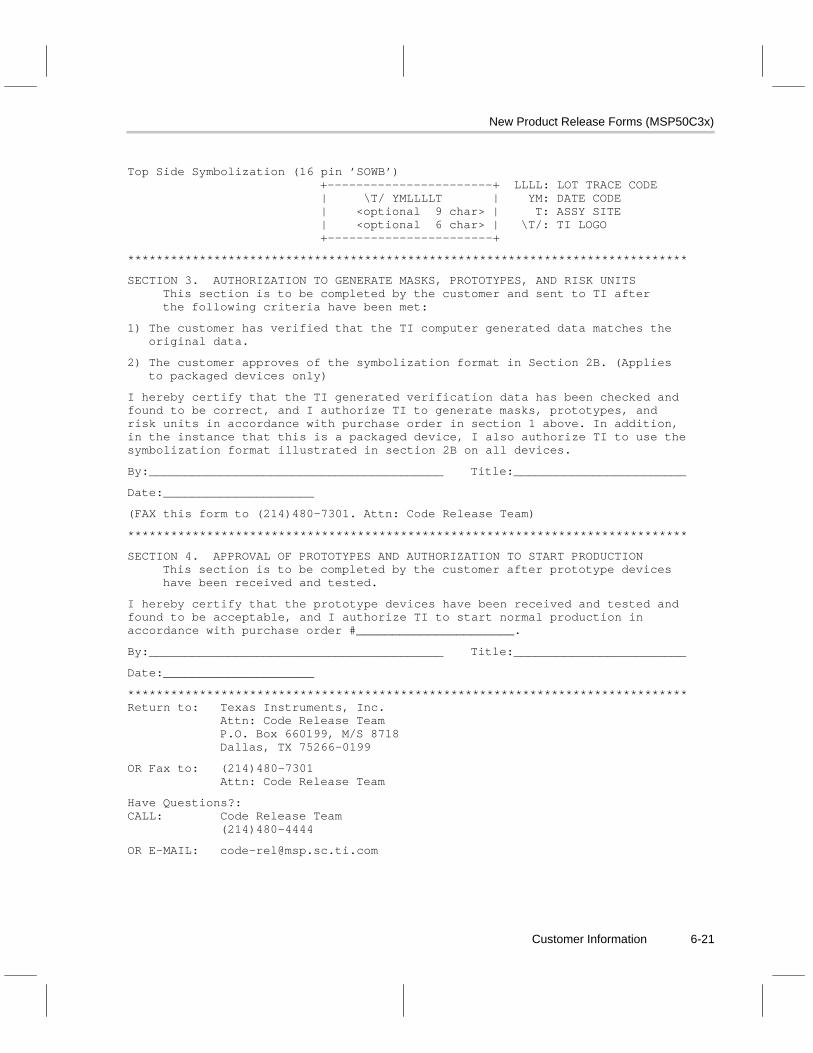
New Product Release Forms (MSP50C3x)
6-21 Customer Information
Top Side Symbolization (16 pin ’SOWB’) +–––––––––––––––––––––––+ LLLL: LOT TRACE CODE | \T/ YMLLLLT | YM: DATE CODE | <optional 9 char> | T: ASSY SITE | <optional 6 char> | \T/: TI LOGO +–––––––––––––––––––––––+
******************************************************************************
SECTION 3. AUTHORIZATION TO GENERATE MASKS, PROTOTYPES, AND RISK UNITS This section is to be completed by the customer and sent to TI after the following criteria have been met:
1) The customer has verified that the TI computer generated data matches the original data.
2) The customer approves of the symbolization format in Section 2B. (Applies to packaged devices only)
I hereby certify that the TI generated verification data has been checked andfound to be correct, and I authorize TI to generate masks, prototypes, andrisk units in accordance with purchase order in section 1 above. In addition,in the instance that this is a packaged device, I also authorize TI to use thesymbolization format illustrated in section 2B on all devices.
By:_________________________________________ Title:________________________
Date:_____________________
(FAX this form to (214)480–7301. Attn: Code Release Team)
******************************************************************************
SECTION 4. APPROVAL OF PROTOTYPES AND AUTHORIZATION TO START PRODUCTION This section is to be completed by the customer after prototype devices have been received and tested.
I hereby certify that the prototype devices have been received and tested andfound to be acceptable, and I authorize TI to start normal production inaccordance with purchase order #______________________.
By:_________________________________________ Title:________________________
Date:_____________________
******************************************************************************Return to: Texas Instruments, Inc. Attn: Code Release Team P.O. Box 660199, M/S 8718 Dallas, TX 75266–0199
OR Fax to: (214)480–7301 Attn: Code Release Team
Have Questions?:CALL: Code Release Team (214)480–4444
OR E–MAIL: code–[email protected]

6-22
A-1
Appendix A
Script Preparation andSpeech Development Tools
Script preparation and speech development can be done either by thecustomer, a third-party consultant, or Texas Instruments. The followingsections discuss major considerations during the script preparation andspeech development process.
Topic Page
A.1 Script Generation A-2. . . . . . . . . . . . . . . . . . . . . . . . . . . . . . . . . . . . . . . . . . . . .
A.2 Speech Development Tools A-5. . . . . . . . . . . . . . . . . . . . . . . . . . . . . . . . . . . .
Appendix A
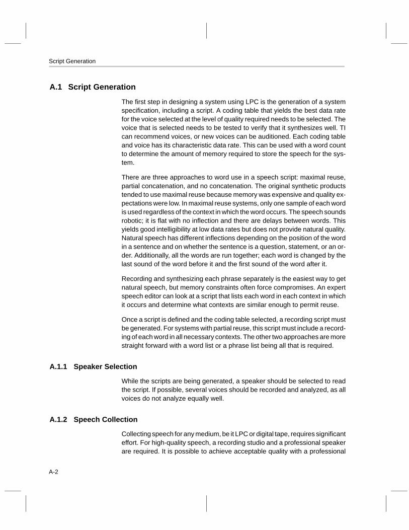
Script Generation
A-2
A.1 Script Generation
The first step in designing a system using LPC is the generation of a systemspecification, including a script. A coding table that yields the best data ratefor the voice selected at the level of quality required needs to be selected. Thevoice that is selected needs to be tested to verify that it synthesizes well. TIcan recommend voices, or new voices can be auditioned. Each coding tableand voice has its characteristic data rate. This can be used with a word countto determine the amount of memory required to store the speech for the sys-tem.
There are three approaches to word use in a speech script: maximal reuse,partial concatenation, and no concatenation. The original synthetic productstended to use maximal reuse because memory was expensive and quality ex-pectations were low. In maximal reuse systems, only one sample of each wordis used regardless of the context in which the word occurs. The speech soundsrobotic; it is flat with no inflection and there are delays between words. Thisyields good intelligibility at low data rates but does not provide natural quality.Natural speech has different inflections depending on the position of the wordin a sentence and on whether the sentence is a question, statement, or an or-der. Additionally, all the words are run together; each word is changed by thelast sound of the word before it and the first sound of the word after it.
Recording and synthesizing each phrase separately is the easiest way to getnatural speech, but memory constraints often force compromises. An expertspeech editor can look at a script that lists each word in each context in whichit occurs and determine what contexts are similar enough to permit reuse.
Once a script is defined and the coding table selected, a recording script mustbe generated. For systems with partial reuse, this script must include a record-ing of each word in all necessary contexts. The other two approaches are morestraight forward with a word list or a phrase list being all that is required.
A.1.1 Speaker Selection
While the scripts are being generated, a speaker should be selected to readthe script. If possible, several voices should be recorded and analyzed, as allvoices do not analyze equally well.
A.1.2 Speech Collection
Collecting speech for any medium, be it LPC or digital tape, requires significanteffort. For high-quality speech, a recording studio and a professional speakerare required. It is possible to achieve acceptable quality with a professional
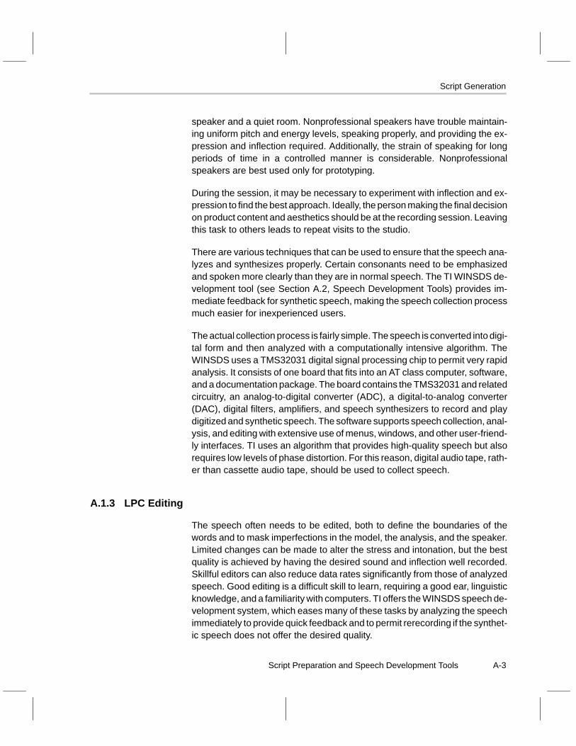
Script Generation
A-3 Script Preparation and Speech Development Tools
speaker and a quiet room. Nonprofessional speakers have trouble maintain-ing uniform pitch and energy levels, speaking properly, and providing the ex-pression and inflection required. Additionally, the strain of speaking for longperiods of time in a controlled manner is considerable. Nonprofessionalspeakers are best used only for prototyping.
During the session, it may be necessary to experiment with inflection and ex-pression to find the best approach. Ideally, the person making the final decisionon product content and aesthetics should be at the recording session. Leavingthis task to others leads to repeat visits to the studio.
There are various techniques that can be used to ensure that the speech ana-lyzes and synthesizes properly. Certain consonants need to be emphasizedand spoken more clearly than they are in normal speech. The TI WINSDS de-velopment tool (see Section A.2, Speech Development Tools) provides im-mediate feedback for synthetic speech, making the speech collection processmuch easier for inexperienced users.
The actual collection process is fairly simple. The speech is converted into digi-tal form and then analyzed with a computationally intensive algorithm. TheWINSDS uses a TMS32031 digital signal processing chip to permit very rapidanalysis. It consists of one board that fits into an AT class computer, software,and a documentation package. The board contains the TMS32031 and relatedcircuitry, an analog-to-digital converter (ADC), a digital-to-analog converter(DAC), digital filters, amplifiers, and speech synthesizers to record and playdigitized and synthetic speech. The software supports speech collection, anal-ysis, and editing with extensive use of menus, windows, and other user-friend-ly interfaces. TI uses an algorithm that provides high-quality speech but alsorequires low levels of phase distortion. For this reason, digital audio tape, rath-er than cassette audio tape, should be used to collect speech.
A.1.3 LPC Editing
The speech often needs to be edited, both to define the boundaries of thewords and to mask imperfections in the model, the analysis, and the speaker.Limited changes can be made to alter the stress and intonation, but the bestquality is achieved by having the desired sound and inflection well recorded.Skillful editors can also reduce data rates significantly from those of analyzedspeech. Good editing is a difficult skill to learn, requiring a good ear, linguisticknowledge, and a familiarity with computers. TI offers the WINSDS speech de-velopment system, which eases many of these tasks by analyzing the speechimmediately to provide quick feedback and to permit rerecording if the synthet-ic speech does not offer the desired quality.

Script Generation
A-4
A.1.4 Pitfalls
All speech interfaces, LPC or not, are human interfaces, so they are hard todesign. Building a prototype system is often useful. The WINSDS supportsquick prototyping.
LPC provides very low data rate speech by virtue of its close modeling of thehuman vocal tract. Nonspeech sounds, such as sound effects, may or may notbe modeled accurately by LPC. The best way to find out whether or not a soundcan be modeled is to record and analyze the sound on the WINSDS.
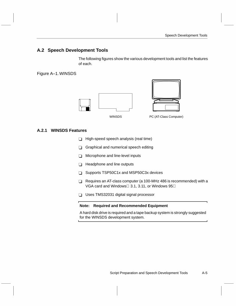
Speech Development Tools
A-5 Script Preparation and Speech Development Tools
A.2 Speech Development Tools
The following figures show the various development tools and list the featuresof each.
Figure A–1.WINSDS
WINSDS PC (AT-Class Computer)
A.2.1 WINSDS Features
High-speed speech analysis (real time)
Graphical and numerical speech editing
Microphone and line-level inputs
Headphone and line outputs
Supports TSP50C1x and MSP50C3x devices
Requires an AT-class computer (a 100-MHz 486 is recommended) with aVGA card and Windows 3.1, 3.11, or Windows 95
Uses TMS32031 digital signal processor
Note: Required and Recommended Equipment
A hard disk drive is required and a tape backup system is strongly suggestedfor the WINSDS development system.
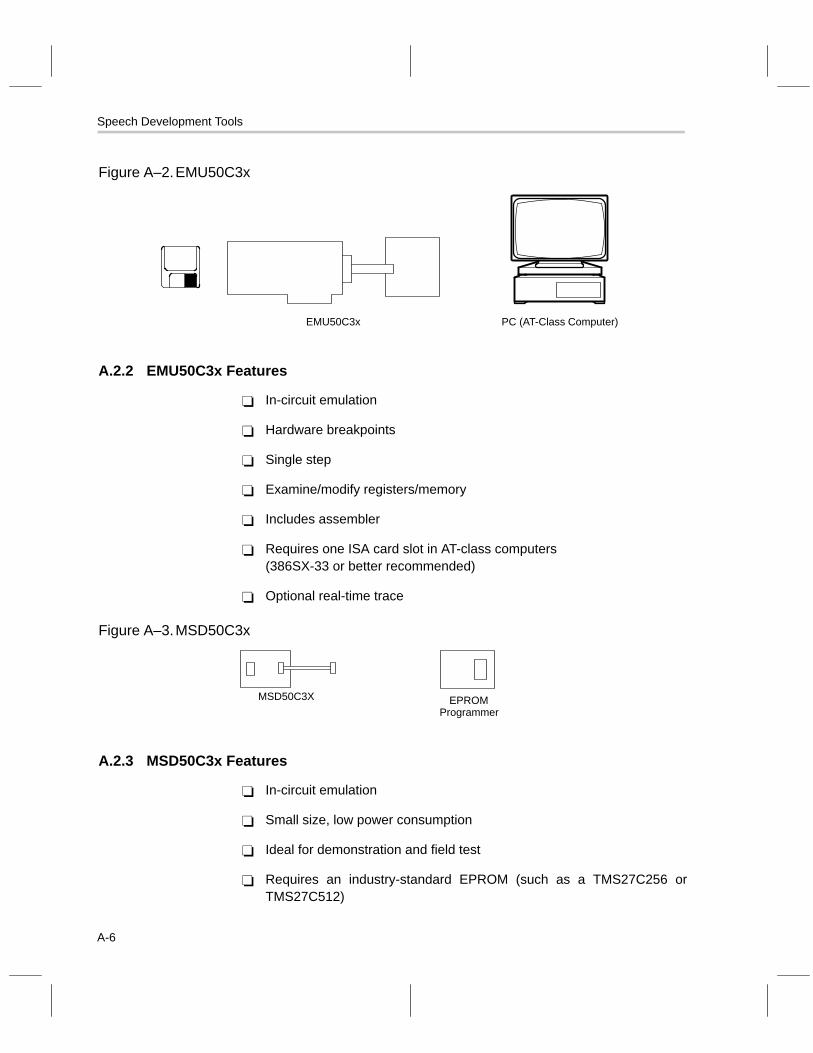
Speech Development Tools
A-6
Figure A–2.EMU50C3x
EMU50C3x PC (AT-Class Computer)
A.2.2 EMU50C3x Features
In-circuit emulation
Hardware breakpoints
Single step
Examine/modify registers/memory
Includes assembler
Requires one ISA card slot in AT-class computers(386SX-33 or better recommended)
Optional real-time trace
Figure A–3.MSD50C3x
EPROMProgrammer
MSD50C3X
A.2.3 MSD50C3x Features
In-circuit emulation
Small size, low power consumption
Ideal for demonstration and field test
Requires an industry-standard EPROM (such as a TMS27C256 orTMS27C512)
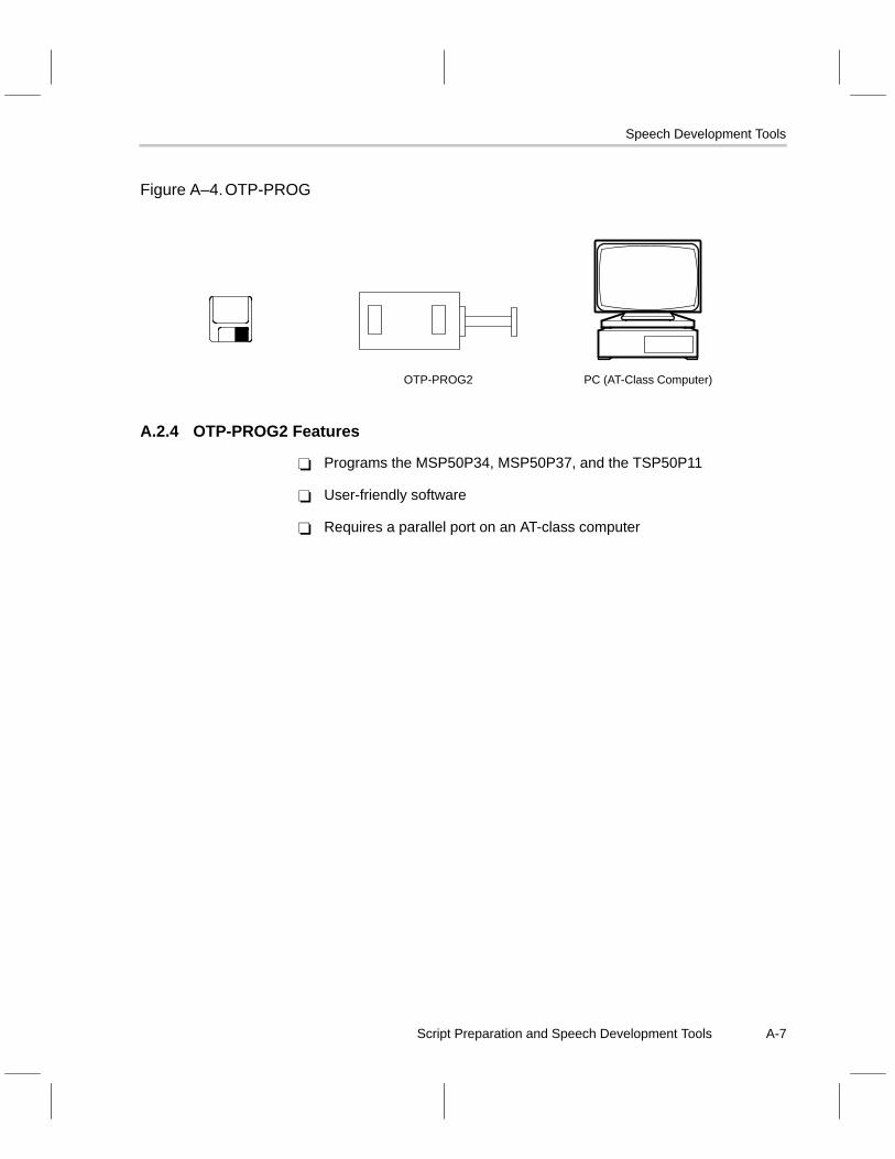
Speech Development Tools
A-7 Script Preparation and Speech Development Tools
Figure A–4.OTP-PROG
OTP-PROG2 PC (AT-Class Computer)
A.2.4 OTP-PROG2 Features
Programs the MSP50P34, MSP50P37, and the TSP50P11
User-friendly software
Requires a parallel port on an AT-class computer

A-8
B-1
Appendix A
MSP50C3x Versus TSP50C1x
This appendix contains information about switching from a TSP50C1x familydevice to a MSP50C3x famly device.
Topic Page
B.1 Summary of Changes from TSP50C1x Family B-2. . . . . . . . . . . . . . . . . . .
B.2 Upgrading a TSP50C1x Program to a MSP50C1x Program B-3. . . . . . . .
Appendix B
Summary of Changes from TSP50C1x Family
B-2
B.1 Summary of Changes from TSP50C1x Family
Support dual LPC capability
RAM size is 256 locations 32 12-bit RAM locations Design part for double clock speed (19.2 MHz) Double mode register to 2 memory mapped 8-bit registers Add dual LPC algorithm Add 2nd Pitch period counter PPC < 0x200 sets the bit in the mode register instead of triggering an
interrupt Level 1 interrupt in LPC mode happens every 30 instruction cycles.
Increase ROM size
Increase Program Counter register width to 16 bits Increase A register width to 16 bits Increase B register width to 16 bits Increase SAR width to 16 bits Increase ROM size to 64 Kbytes
Miscellaneous
No support for external ROM mode Improved internal oscillator design Improved D/A output design Designed part for increased VDD range (3.3V – 6.5V) Remap A port to 0xFCh – 0xFFh RAM range Remap B port to 0xF8h – 0xFBh RAM range Added wakeup function 3 oscillator modes (internal, external, and crystal/ceramic) Status gets set by SETOFF, INIT terminal low, and interrupt Fix DECMN instruction so that true decrement happens on 12-bit
RAM Fix ANDCM instruction so that operation on 12-bit RAM location does
not affect the upper 4 bits SETOFF does not change the I/O state Memory map mode registers I/O ports are paged in and out of the memory map by the IO_MAP bit
in the Mode Register Interrupt vector location is changed
Upgrading a TSP50C1x Program to a MSP50C3x Program
B-3 MPS50C1x Versus TSP50C1x
B.2 Upgrading a TSP50C1x Program to a MSP50C3x Program
This section documents the changes necessary to upgrade a TSP50C1x pro-gram to a MSP50C3x program. This file assumes that none of the additionalfeatures of the MSP50C3x are being used. for example, the wakeup functiondoes not exist on the TSP50C1x, so code changes necessary to accommo-date the wakeup function are not included.
Assumptions:
The wakeup function is not used Only the A and B ports are used Only 128 RAM locations or less are used Only 16-K ROM locations are used All program code is in the lower 4 Kbytes of ROM
B.2.1 Normal Operation
Remap interrupt vectors
The interrupt vectors are I/O mapped in a different sequence on theMSP50C3x than they are on the TSP50C1x.
Table B–1.Interrupt Vectors for the TSP50C1x and the MSP50C3x
Address Type TSP50C1x MSP50C3x
0x0010 Level 2 Interrupt PCM = 0, LPC = 1 PCM = 0, LPC = 0
0x0012 Level 2 Interrupt PCM = 0, LPC = 0 PCM = 0, LPC = 1
0x0014 Level 2 Interrupt PCM = 1, LPC = 1 PCM = 1, LPC = 0
0x0016 Level 2 Interrupt PCM = 1, LPC = 0 PCM = 1, LPC = 1
0x0018 Level 1 Interrupt PCM = 0, LPC = 1 PCM = 0, LPC = 0
0x001A Level 1 Interrupt PCM = 0, LPC = 0 PCM = 0, LPC = 1
0x001C Level 1 Interrupt PCM = 1, LPC = 1 PCM = 1, LPC = 0
0x001E Level 1 Interrupt PCM = 1, LPC = 0 PCM = 1, LPC = 1
Remap I/O ports
The I/O ports are I/O mapped to different RAM locations on the MSP50C3xthan they are on the TSP50C1x.
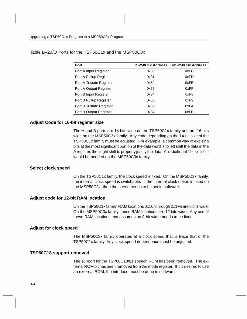
Upgrading a TSP50C1x Program to a MSP50C3x Program
B-4
Table B–2.I/O Ports for the TSP50C1x and the MSP50C3x
Port TSP50C1x Address MSP50C3x Address
Port A Input Register 0x80 0xFC
Port A Pullup Register 0x81 0xFD
Port A Tristate Register 0x82 0xFE
Port A Output Register 0x83 0xFF
Port B Input Register 0x84 0xF8
Port B Pullup Register 0x85 0xF9
Port B Tristate Register 0x86 0xFA
Port B Output Register 0x87 0xFB
Adjust Code for 16-bit register size
The A and B ports are 14 bits wide on the TSP50C1x family and are 16 bitswide on the MSP50C3x family. Any code depending on the 14-bit size of theTSP50C1x family must be adjusted. For example, a common way of excisingbits at the most significant portion of the data word is to left shift the data in theA register, then right shift to properly justify the data. An additional 2 bits of shiftwould be needed on the MSP50C3x family.
Select clock speed
On the TSP50C1x family, the clock speed is fixed. On the MSP50C3x family,the internal clock speed is switchable. If the internal clock option is used onthe MSP50C3x, then the speed needs to be set in software.
Adjust code for 12-bit RAM location
On the TSP50C1x family, RAM locations 0x10h through 0x1Fh are 8 bits wide.On the MSP50C3x family, these RAM locations are 12 bits wide. Any use ofthese RAM locations that assumes an 8-bit width needs to be fixed.
Adjust for clock speed
The MSP50C3x family operates at a clock speed that is twice that of theTSP50C1x family. Any clock speed dependence must be adjusted.
TSP60C18 support removed
The support for the TSP60C18/81 speech ROM has been removed. The ex-ternal ROM bit has been removed from the mode register. If it is desired to usean external ROM, the interface must be done in software.
Upgrading a TSP50C1x Program to a MSP50C3x Program
B-5 MPS50C1x Versus TSP50C1x
Adjust code for 12-bit X register size
On the TSP50C1x family, the X register is 8 bits wide. On the MSP50C3x fami-ly, the X register is 12 bits wide. Any use of the X register that assumes an 8-bitwidth needs to be fixed.
Converting TSP50C19 code
There is no paging on the MSP50C3x family.
B.2.2 LPC
Adjust code for different LPC interrupt
On the TSP50C1x family, the LPC interrupt was caused by the underflow ofthe pitch period counter. On the MSP50C3x family, the LPC interrupt is in-voked at a 20-kHz rate by the system clock. The underflow of the pitch periodcounter causes a bit to be set to 1 in mode register 2.
Modify the MSP50C3x code to periodically poll the mode register for the PPCbit to be set and then clear the bit and either branch or call the interpolationroutine.
Clear Memory-Mapped Register prior to turning on LPC
RAM locations 0xFF0h, 0xFF1h, 0xFF2h, and 0xFF4h should be cleared to 0prior to turning on the LPC. The RAM location 0xFF3h should be set to 0x162h.
Replace the excitation function with the MSP50C3x excitation function.
Thie excitation function is the same as the TSP50C1x excitation function ex-cept that the unvoiced portion (#3A80) is sign extended to 16 bits (#FA80). Thevoiced portion of the excitation function may need to be multiplied by 2 to getthe same volume as the TSP50C1x.
Move the excitation function
In TSP50C1x programs (except the TSP50C19), the excitation function needsto be moved from 0x4000 to 0x8000 when using the MSP50C33 or to 0x10000when using the MSP50C34.
Note: TSP50C19
On the TSP50C19, the excitation function already has been moved to0x8000h.
Upgrading a TSP50C1x Program to a MSP50C3x Program
B-6
B.2.3 PCM
Adjust data for the different register size
On the TSP50C1x family, the TASYN instruction loaded the PCM data to a reg-ister 14 bits wide. The least significant 2 bits were unused and the most signifi-cant 2 bits were used for sign extension.
On the MSP50C3x family, the TASYN instruction loads the PCM data to a reg-ister 16 bits wide. The least-significant two bits are unused. The most signifi-cant two bits are used for overflow with the third most-significant bit being usedfor sign extension.
C-1
Appendix A
MSP50C3x Sample Dual Synthesis Program
Topic Page
C.1 MSP50C3x Sample Dual Synthesis Program C-2. . . . . . . . . . . . . . . . . . . .
Appendix C
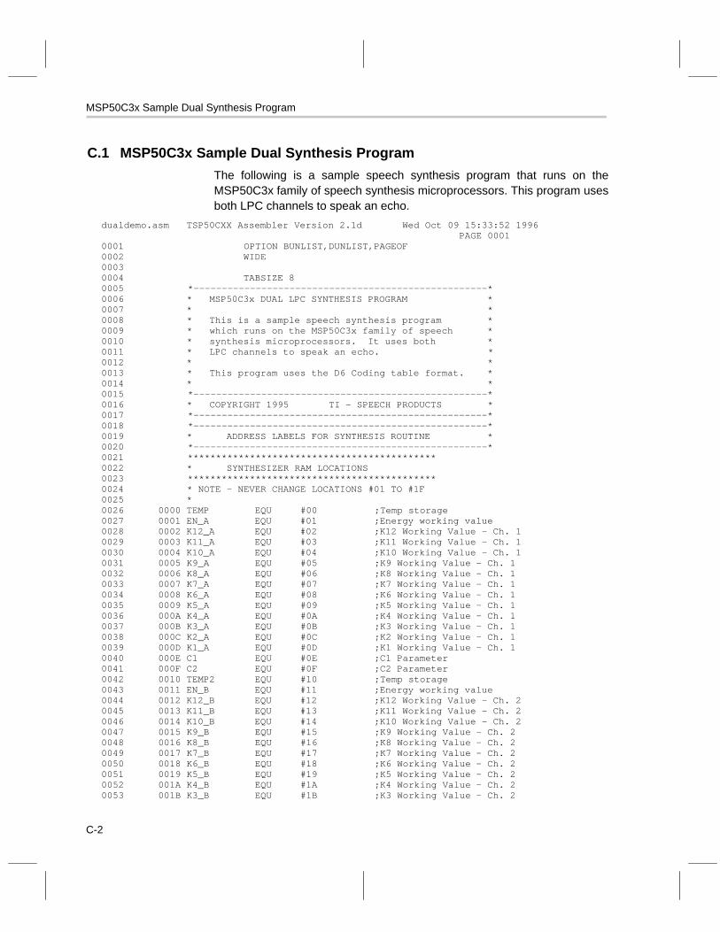
MSP50C3x Sample Dual Synthesis Program
C-2
C.1 MSP50C3x Sample Dual Synthesis Program
The following is a sample speech synthesis program that runs on theMSP50C3x family of speech synthesis microprocessors. This program usesboth LPC channels to speak an echo.
dualdemo.asm TSP50CXX Assembler Version 2.1d Wed Oct 09 15:33:52 1996 PAGE 00010001 OPTION BUNLIST,DUNLIST,PAGEOF0002 WIDE00030004 TABSIZE 80005 *––––––––––––––––––––––––––––––––––––––––––––––––––––*0006 * MSP50C3x DUAL LPC SYNTHESIS PROGRAM *0007 * *0008 * This is a sample speech synthesis program *0009 * which runs on the MSP50C3x family of speech *0010 * synthesis microprocessors. It uses both *0011 * LPC channels to speak an echo. *0012 * *0013 * This program uses the D6 Coding table format. *0014 * *0015 *––––––––––––––––––––––––––––––––––––––––––––––––––––*0016 * COPYRIGHT 1995 TI – SPEECH PRODUCTS *0017 *––––––––––––––––––––––––––––––––––––––––––––––––––––*0018 *––––––––––––––––––––––––––––––––––––––––––––––––––––*0019 * ADDRESS LABELS FOR SYNTHESIS ROUTINE *0020 *––––––––––––––––––––––––––––––––––––––––––––––––––––*0021 ********************************************0022 * SYNTHESIZER RAM LOCATIONS0023 ********************************************0024 * NOTE – NEVER CHANGE LOCATIONS #01 TO #1F0025 *0026 0000 TEMP EQU #00 ;Temp storage0027 0001 EN_A EQU #01 ;Energy working value0028 0002 K12_A EQU #02 ;K12 Working Value – Ch. 10029 0003 K11_A EQU #03 ;K11 Working Value – Ch. 10030 0004 K10_A EQU #04 ;K10 Working Value – Ch. 10031 0005 K9_A EQU #05 ;K9 Working Value – Ch. 10032 0006 K8_A EQU #06 ;K8 Working Value – Ch. 10033 0007 K7_A EQU #07 ;K7 Working Value – Ch. 10034 0008 K6_A EQU #08 ;K6 Working Value – Ch. 10035 0009 K5_A EQU #09 ;K5 Working Value – Ch. 10036 000A K4_A EQU #0A ;K4 Working Value – Ch. 10037 000B K3_A EQU #0B ;K3 Working Value – Ch. 10038 000C K2_A EQU #0C ;K2 Working Value – Ch. 10039 000D K1_A EQU #0D ;K1 Working Value – Ch. 10040 000E C1 EQU #0E ;C1 Parameter0041 000F C2 EQU #0F ;C2 Parameter0042 0010 TEMP2 EQU #10 ;Temp storage0043 0011 EN_B EQU #11 ;Energy working value0044 0012 K12_B EQU #12 ;K12 Working Value – Ch. 20045 0013 K11_B EQU #13 ;K11 Working Value – Ch. 20046 0014 K10_B EQU #14 ;K10 Working Value – Ch. 20047 0015 K9_B EQU #15 ;K9 Working Value – Ch. 20048 0016 K8_B EQU #16 ;K8 Working Value – Ch. 20049 0017 K7_B EQU #17 ;K7 Working Value – Ch. 20050 0018 K6_B EQU #18 ;K6 Working Value – Ch. 20051 0019 K5_B EQU #19 ;K5 Working Value – Ch. 20052 001A K4_B EQU #1A ;K4 Working Value – Ch. 20053 001B K3_B EQU #1B ;K3 Working Value – Ch. 2
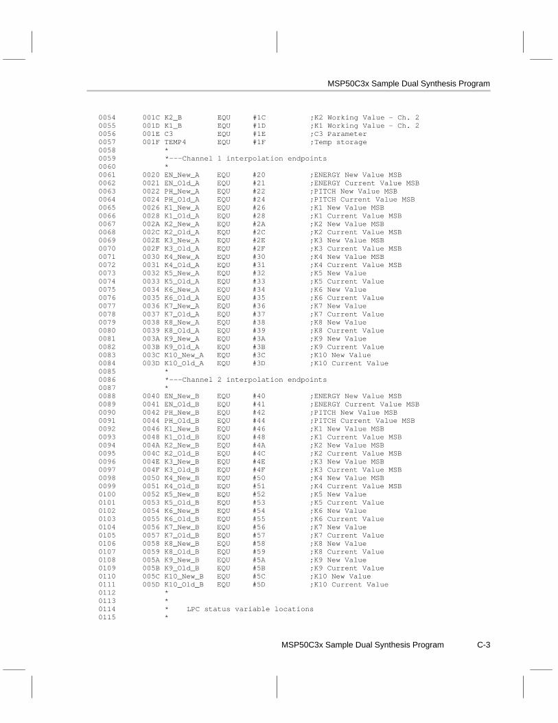
MSP50C3x Sample Dual Synthesis Program
C-3 MSP50C3x Sample Dual Synthesis Program
0054 001C K2_B EQU #1C ;K2 Working Value – Ch. 20055 001D K1_B EQU #1D ;K1 Working Value – Ch. 20056 001E C3 EQU #1E ;C3 Parameter0057 001F TEMP4 EQU #1F ;Temp storage0058 *0059 *–––Channel 1 interpolation endpoints0060 *0061 0020 EN_New_A EQU #20 ;ENERGY New Value MSB0062 0021 EN_Old_A EQU #21 ;ENERGY Current Value MSB0063 0022 PH_New_A EQU #22 ;PITCH New Value MSB0064 0024 PH_Old_A EQU #24 ;PITCH Current Value MSB0065 0026 K1_New_A EQU #26 ;K1 New Value MSB0066 0028 K1_Old_A EQU #28 ;K1 Current Value MSB0067 002A K2_New_A EQU #2A ;K2 New Value MSB0068 002C K2_Old_A EQU #2C ;K2 Current Value MSB0069 002E K3_New_A EQU #2E ;K3 New Value MSB0070 002F K3_Old_A EQU #2F ;K3 Current Value MSB0071 0030 K4_New_A EQU #30 ;K4 New Value MSB0072 0031 K4_Old_A EQU #31 ;K4 Current Value MSB0073 0032 K5_New_A EQU #32 ;K5 New Value0074 0033 K5_Old_A EQU #33 ;K5 Current Value0075 0034 K6_New_A EQU #34 ;K6 New Value0076 0035 K6_Old_A EQU #35 ;K6 Current Value0077 0036 K7_New_A EQU #36 ;K7 New Value0078 0037 K7_Old_A EQU #37 ;K7 Current Value0079 0038 K8_New_A EQU #38 ;K8 New Value0080 0039 K8_Old_A EQU #39 ;K8 Current Value0081 003A K9_New_A EQU #3A ;K9 New Value0082 003B K9_Old_A EQU #3B ;K9 Current Value0083 003C K10_New_A EQU #3C ;K10 New Value0084 003D K10_Old_A EQU #3D ;K10 Current Value0085 *0086 *–––Channel 2 interpolation endpoints0087 *0088 0040 EN_New_B EQU #40 ;ENERGY New Value MSB0089 0041 EN_Old_B EQU #41 ;ENERGY Current Value MSB0090 0042 PH_New_B EQU #42 ;PITCH New Value MSB0091 0044 PH_Old_B EQU #44 ;PITCH Current Value MSB0092 0046 K1_New_B EQU #46 ;K1 New Value MSB0093 0048 K1_Old_B EQU #48 ;K1 Current Value MSB0094 004A K2_New_B EQU #4A ;K2 New Value MSB0095 004C K2_Old_B EQU #4C ;K2 Current Value MSB0096 004E K3_New_B EQU #4E ;K3 New Value MSB0097 004F K3_Old_B EQU #4F ;K3 Current Value MSB0098 0050 K4_New_B EQU #50 ;K4 New Value MSB0099 0051 K4_Old_B EQU #51 ;K4 Current Value MSB0100 0052 K5_New_B EQU #52 ;K5 New Value0101 0053 K5_Old_B EQU #53 ;K5 Current Value0102 0054 K6_New_B EQU #54 ;K6 New Value0103 0055 K6_Old_B EQU #55 ;K6 Current Value0104 0056 K7_New_B EQU #56 ;K7 New Value0105 0057 K7_Old_B EQU #57 ;K7 Current Value0106 0058 K8_New_B EQU #58 ;K8 New Value0107 0059 K8_Old_B EQU #59 ;K8 Current Value0108 005A K9_New_B EQU #5A ;K9 New Value0109 005B K9_Old_B EQU #5B ;K9 Current Value0110 005C K10_New_B EQU #5C ;K10 New Value0111 005D K10_Old_B EQU #5D ;K10 Current Value0112 *0113 *0114 * LPC status variable locations0115 *
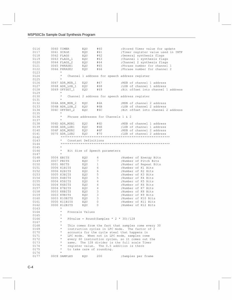
MSP50C3x Sample Dual Synthesis Program
C-4
0116 0060 TIMER EQU #60 ;Stored Timer value for update0117 0061 SCALE EQU #61 ;Timer register value used in INTP0118 0062 FLAGS EQU #62 ;General synthesis flags0119 0063 FLAGS_1 EQU #63 ;Channel 1 synthesis flags0120 0064 FLAGS_2 EQU #64 ;Channel 2 synthesis flags0121 0065 PHRASE1 EQU #65 ;Phrase number for channel 10122 0066 PHRASE2 EQU #66 ;Phrase number for channel 20123 *0124 * Channel 1 address for speech address register0125 *0126 0067 ADR_MSB_1 EQU #67 ;MSB of channel 1 address0127 0068 ADR_LSB_1 EQU #68 ;LSB of channel 1 address0128 0069 OFFSET_1 EQU #69 ;Bit offset into channel 1 address0129 *0130 * Channel 2 address for speech address register0131 *0132 006A ADR_MSB_2 EQU #6A ;MSB of channel 2 address0133 006B ADR_LSB_2 EQU #6B ;LSB of channel 2 address0134 006C OFFSET_2 EQU #6C ;Bit offset into channel 2 address0135 *0136 * Phrase addresses for Channels 1 & 20137 *0138 006D ADR_MSB1 EQU #6D ;MSB of channel 1 address0139 006E ADR_LSB1 EQU #6E ;LSB of channel 1 address0140 006F ADR_MSB2 EQU #6F ;MSB of channel 2 address0141 0070 ADR_LSB2 EQU #70 ;LSB of channel 2 address0142 ************************************************************0143 * Constant Definitions0144 ************************************************************0145 *0146 * Bit Size of Speech parameters0147 *0148 0004 EBITS EQU 4 ;Number of Energy Bits0149 0007 PBITS EQU 7 ;Number of Pitch Bits0150 0001 RBITS EQU 1 ;Number of Repeat Bits0151 0006 K1BITS EQU 6 ;Number of K1 Bits0152 0006 K2BITS EQU 6 ;Number of K2 Bits0153 0005 K3BITS EQU 5 ;Number of K3 Bits0154 0005 K4BITS EQU 5 ;Number of K4 Bits0155 0004 K5BITS EQU 4 ;Number of K5 Bits0156 0004 K6BITS EQU 4 ;Number of K6 Bits0157 0004 K7BITS EQU 4 ;Number of K7 Bits0158 0003 K8BITS EQU 3 ;Number of K8 Bits0159 0003 K9BITS EQU 3 ;Number of K9 Bits0160 0003 K10BITS EQU 3 ;Number of K10 Bits0161 0000 K11BITS EQU 0 ;Number of K11 Bits0162 0000 K12BITS EQU 0 ;Number of K12 Bits0163 *0164 * Prescale Values0165 *0166 * PSvalue = Round(Samples * 2 * 30)/1280167 *0168 * This comes from the fact that samples come every 300169 * instruction cycles in LPC mode. The factor of 20170 * accounts for the cycle steal that happens in0171 * LPC mode. When not in LPC mode, samples come0172 * every 60 instruction cycles, so it comes out the0173 * same. The 128 divider is the full scale Timer0174 * register value. The 0.5 addition is there0175 * to take care of rounding.0176 *0177 00C8 SAMPLES EQU 200 ;Samples per frame
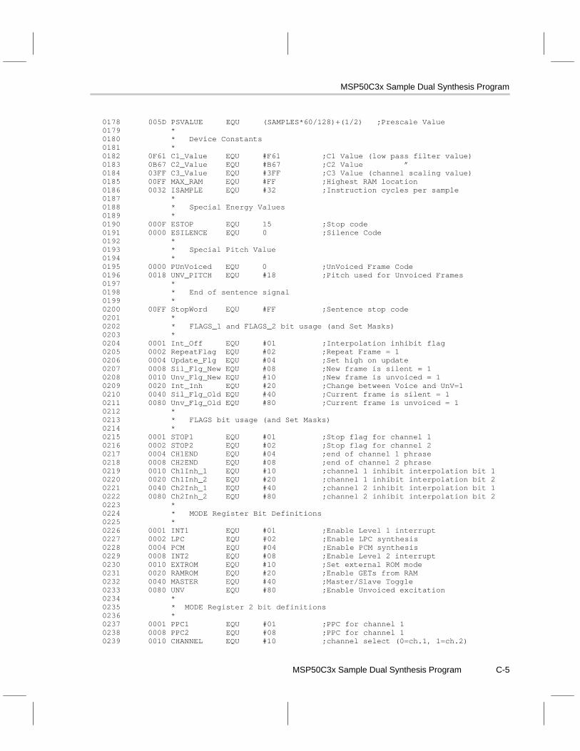
MSP50C3x Sample Dual Synthesis Program
C-5 MSP50C3x Sample Dual Synthesis Program
0178 005D PSVALUE EQU (SAMPLES*60/128)+(1/2) ;Prescale Value0179 *0180 * Device Constants0181 *0182 0F61 C1_Value EQU #F61 ;C1 Value (low pass filter value)0183 0B67 C2_Value EQU #B67 ;C2 Value ”0184 03FF C3_Value EQU #3FF ;C3 Value (channel scaling value)0185 00FF MAX_RAM EQU #FF ;Highest RAM location0186 0032 ISAMPLE EQU #32 ;Instruction cycles per sample0187 *0188 * Special Energy Values0189 *0190 000F ESTOP EQU 15 ;Stop code0191 0000 ESILENCE EQU 0 ;Silence Code0192 *0193 * Special Pitch Value0194 *0195 0000 PUnVoiced EQU 0 ;UnVoiced Frame Code0196 0018 UNV_PITCH EQU #18 ;Pitch used for Unvoiced Frames0197 *0198 * End of sentence signal0199 *0200 00FF StopWord EQU #FF ;Sentence stop code0201 *0202 * FLAGS_1 and FLAGS_2 bit usage (and Set Masks)0203 *0204 0001 Int_Off EQU #01 ;Interpolation inhibit flag0205 0002 RepeatFlag EQU #02 ;Repeat Frame = 10206 0004 Update_Flg EQU #04 ;Set high on update0207 0008 Sil_Flg_New EQU #08 ;New frame is silent = 10208 0010 Unv_Flg_New EQU #10 ;New frame is unvoiced = 10209 0020 Int_Inh EQU #20 ;Change between Voice and UnV=10210 0040 Sil_Flg_Old EQU #40 ;Current frame is silent = 10211 0080 Unv_Flg_Old EQU #80 ;Current frame is unvoiced = 10212 *0213 * FLAGS bit usage (and Set Masks)0214 *0215 0001 STOP1 EQU #01 ;Stop flag for channel 10216 0002 STOP2 EQU #02 ;Stop flag for channel 20217 0004 CH1END EQU #04 ;end of channel 1 phrase0218 0008 CH2END EQU #08 ;end of channel 2 phrase0219 0010 Ch1Inh_1 EQU #10 ;channel 1 inhibit interpolation bit 10220 0020 Ch1Inh_2 EQU #20 ;channel 1 inhibit interpolation bit 20221 0040 Ch2Inh_1 EQU #40 ;channel 2 inhibit interpolation bit 10222 0080 Ch2Inh_2 EQU #80 ;channel 2 inhibit interpolation bit 20223 *0224 * MODE Register Bit Definitions0225 *0226 0001 INT1 EQU #01 ;Enable Level 1 interrupt0227 0002 LPC EQU #02 ;Enable LPC synthesis0228 0004 PCM EQU #04 ;Enable PCM synthesis0229 0008 INT2 EQU #08 ;Enable Level 2 interrupt0230 0010 EXTROM EQU #10 ;Set external ROM mode0231 0020 RAMROM EQU #20 ;Enable GETs from RAM0232 0040 MASTER EQU #40 ;Master/Slave Toggle0233 0080 UNV EQU #80 ;Enable Unvoiced excitation0234 *0235 * MODE Register 2 bit definitions0236 *0237 0001 PPC1 EQU #01 ;PPC for channel 10238 0008 PPC2 EQU #08 ;PPC for channel 10239 0010 CHANNEL EQU #10 ;channel select (0=ch.1, 1=ch.2)
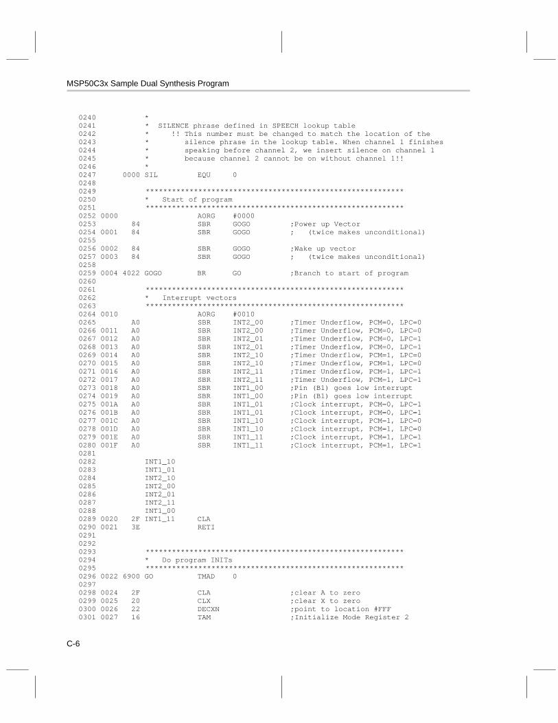
MSP50C3x Sample Dual Synthesis Program
C-6
0240 *0241 * SILENCE phrase defined in SPEECH lookup table0242 * !! This number must be changed to match the location of the0243 * silence phrase in the lookup table. When channel 1 finishes0244 * speaking before channel 2, we insert silence on channel 10245 * because channel 2 cannot be on without channel 1!!0246 *0247 0000 SIL EQU 002480249 ***********************************************************0250 * Start of program0251 ***********************************************************0252 0000 AORG #00000253 84 SBR GOGO ;Power up Vector0254 0001 84 SBR GOGO ; (twice makes unconditional)02550256 0002 84 SBR GOGO ;Wake up vector0257 0003 84 SBR GOGO ; (twice makes unconditional)02580259 0004 4022 GOGO BR GO ;Branch to start of program02600261 ***********************************************************0262 * Interrupt vectors0263 ***********************************************************0264 0010 AORG #00100265 A0 SBR INT2_00 ;Timer Underflow, PCM=0, LPC=00266 0011 A0 SBR INT2_00 ;Timer Underflow, PCM=0, LPC=00267 0012 A0 SBR INT2_01 ;Timer Underflow, PCM=0, LPC=10268 0013 A0 SBR INT2_01 ;Timer Underflow, PCM=0, LPC=10269 0014 A0 SBR INT2_10 ;Timer Underflow, PCM=1, LPC=00270 0015 A0 SBR INT2_10 ;Timer Underflow, PCM=1, LPC=00271 0016 A0 SBR INT2_11 ;Timer Underflow, PCM=1, LPC=10272 0017 A0 SBR INT2_11 ;Timer Underflow, PCM=1, LPC=10273 0018 A0 SBR INT1_00 ;Pin (B1) goes low interrupt0274 0019 A0 SBR INT1_00 ;Pin (B1) goes low interrupt0275 001A A0 SBR INT1_01 ;Clock interrupt, PCM=0, LPC=10276 001B A0 SBR INT1_01 ;Clock interrupt, PCM=0, LPC=10277 001C A0 SBR INT1_10 ;Clock interrupt, PCM=1, LPC=00278 001D A0 SBR INT1_10 ;Clock interrupt, PCM=1, LPC=00279 001E A0 SBR INT1_11 ;Clock interrupt, PCM=1, LPC=10280 001F A0 SBR INT1_11 ;Clock interrupt, PCM=1, LPC=102810282 INT1_100283 INT1_010284 INT2_100285 INT2_000286 INT2_010287 INT2_110288 INT1_000289 0020 2F INT1_11 CLA0290 0021 3E RETI029102920293 ***********************************************************0294 * Do program INITs0295 ***********************************************************0296 0022 6900 GO TMAD 002970298 0024 2F CLA ;clear A to zero0299 0025 20 CLX ;clear X to zero0300 0026 22 DECXN ;point to location #FFF0301 0027 16 TAM ;Initialize Mode Register 2

MSP50C3x Sample Dual Synthesis Program
C-7 MSP50C3x Sample Dual Synthesis Program
0302 0028 22 DECXN ;point to location #FFE0303 0029 16 TAM ;Initialize Mode Register 103040305 002A 20 CLX ;clear X to zero0306 002B 13 RAM_LOOP TAMIX ;Initialize All RAM to zeros0307 002C 61FF XGEC MAX_RAM ;all RAM initialized?0308 002E 4032 BR RAM_EXIT ; yes, exit loop0309 0030 402B BR RAM_LOOP ; no, continue looping03100311 0032 16 RAM_EXIT TAM ;initialize last RAM loaction (FF)03120313 0033 6E01 TCA 1 ;Speak 2nd phrase on channel 20314 0035 1A TAB0315 0036 6E00 TCA 0 ;Speak 1st phrase on channel 10316 0038 003B CALL SPEAK03170318 003A 3F setoff ;shut down0319 ***********************************************************0320 * Speak Utterance – Phrase numbers in A & B registers0321 ***********************************************************0322 003B 3B SPEAK INTGR03230324 003C 6A65 TAMD PHRASE1 ;Store channel 1 phrase number0325 003E 12 XBA ;retrieve 2nd phrase number0326 003F 6A66 TAMD PHRASE2 ;Store channel 2 phrase number03270328 0041 2F CLA0329 0042 6A62 TAMD FLAGS ;Init flags for speech0330 0044 6A63 TAMD FLAGS_10331 0046 6A64 TAMD FLAGS_203320333 *–––––Initialize address for channel 1–––––*03340335 0048 6965 LOOKUP1 TMAD PHRASE1 ;Fetch stored phrase number0336 004A 2E SALA ;Double index to get offset0337 004B 79E9 ACAAC SENTENCE ;Add base of table03380339 004D 6D LUAB ;get address MSB0340 004E 3A IAC ;point to address LSB0341 004F 6B LUAA ;get address LSB0342 0050 12 XBA ;move LSB to B & MSB to A0343 0051 1B SALA4 ;combine MSB and LSB0344 0052 1B SALA4 ; into complete address0345 0053 2C ABAAC0346 0054 6A6E TAMD ADR_LSB1 ;save address LSB0347 0056 6801 AXCA 1 ;isolate next address MSB (shift by 8)0348 0058 15 SARA0349 0059 6A6D TAMD ADR_MSB1 ;save address MSB03500351 *–––––Initialize address for channel 203520353 LOOKUP20354 005B 6966 TMAD PHRASE2 ;Fetch stored phrase number0355 005D 2E SALA ;Double index to get offset0356 005E 79E9 ACAAC SENTENCE ;Add base of table03570358 0060 6D LUAB ;get address MSB0359 0061 3A IAC ;point to address LSB0360 0062 6B LUAA ;get address LSB0361 0063 12 XBA ;move LSB to B & MSB to A0362 0064 1B SALA4 ;combine MSB and LSB0363 0065 1B SALA4 ; into complete address
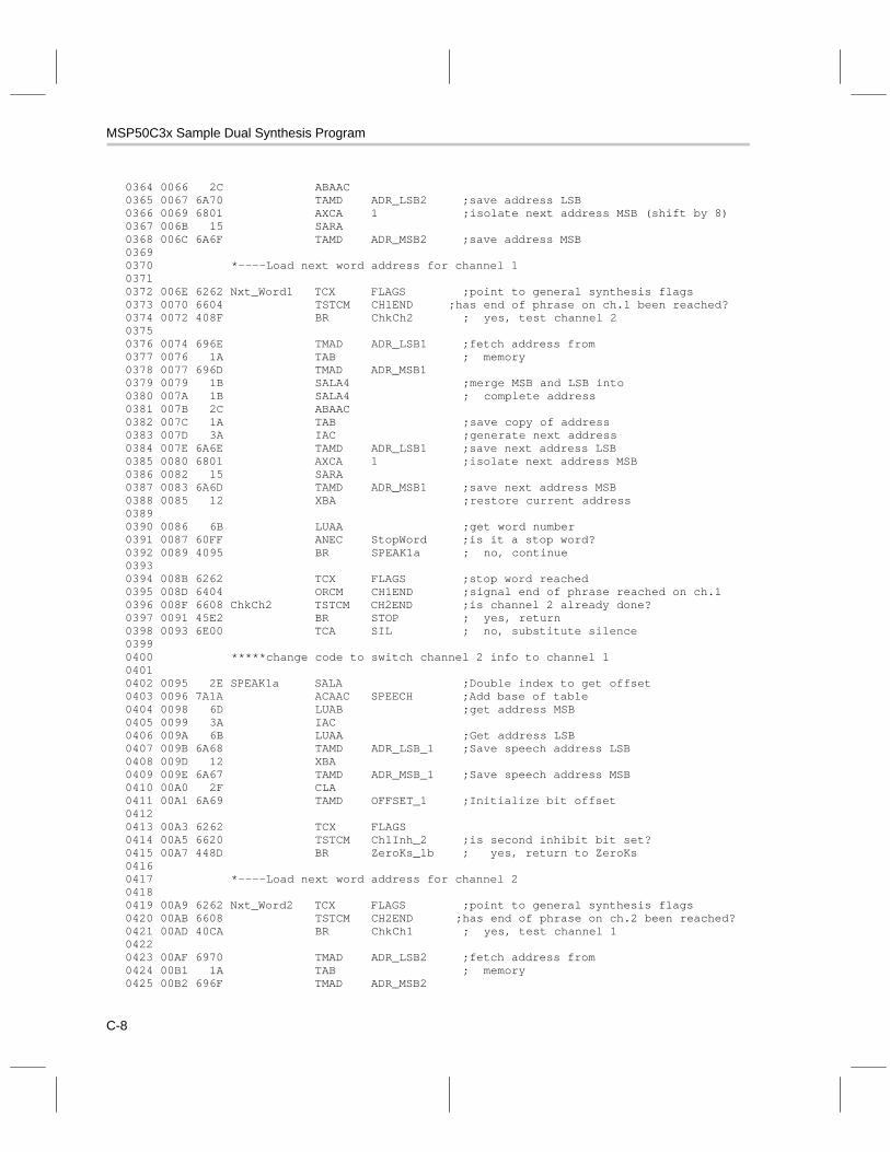
MSP50C3x Sample Dual Synthesis Program
C-8
0364 0066 2C ABAAC0365 0067 6A70 TAMD ADR_LSB2 ;save address LSB0366 0069 6801 AXCA 1 ;isolate next address MSB (shift by 8)0367 006B 15 SARA0368 006C 6A6F TAMD ADR_MSB2 ;save address MSB03690370 *––––Load next word address for channel 103710372 006E 6262 Nxt_Word1 TCX FLAGS ;point to general synthesis flags0373 0070 6604 TSTCM CH1END ;has end of phrase on ch.1 been reached?0374 0072 408F BR ChkCh2 ; yes, test channel 203750376 0074 696E TMAD ADR_LSB1 ;fetch address from0377 0076 1A TAB ; memory0378 0077 696D TMAD ADR_MSB10379 0079 1B SALA4 ;merge MSB and LSB into0380 007A 1B SALA4 ; complete address0381 007B 2C ABAAC0382 007C 1A TAB ;save copy of address0383 007D 3A IAC ;generate next address0384 007E 6A6E TAMD ADR_LSB1 ;save next address LSB0385 0080 6801 AXCA 1 ;isolate next address MSB0386 0082 15 SARA0387 0083 6A6D TAMD ADR_MSB1 ;save next address MSB0388 0085 12 XBA ;restore current address03890390 0086 6B LUAA ;get word number0391 0087 60FF ANEC StopWord ;is it a stop word?0392 0089 4095 BR SPEAK1a ; no, continue03930394 008B 6262 TCX FLAGS ;stop word reached0395 008D 6404 ORCM CH1END ;signal end of phrase reached on ch.10396 008F 6608 ChkCh2 TSTCM CH2END ;is channel 2 already done?0397 0091 45E2 BR STOP ; yes, return0398 0093 6E00 TCA SIL ; no, substitute silence03990400 *****change code to switch channel 2 info to channel 104010402 0095 2E SPEAK1a SALA ;Double index to get offset0403 0096 7A1A ACAAC SPEECH ;Add base of table0404 0098 6D LUAB ;get address MSB0405 0099 3A IAC0406 009A 6B LUAA ;Get address LSB0407 009B 6A68 TAMD ADR_LSB_1 ;Save speech address LSB0408 009D 12 XBA0409 009E 6A67 TAMD ADR_MSB_1 ;Save speech address MSB0410 00A0 2F CLA0411 00A1 6A69 TAMD OFFSET_1 ;Initialize bit offset04120413 00A3 6262 TCX FLAGS0414 00A5 6620 TSTCM Ch1Inh_2 ;is second inhibit bit set?0415 00A7 448D BR ZeroKs_1b ; yes, return to ZeroKs04160417 *––––Load next word address for channel 204180419 00A9 6262 Nxt_Word2 TCX FLAGS ;point to general synthesis flags0420 00AB 6608 TSTCM CH2END ;has end of phrase on ch.2 been reached?0421 00AD 40CA BR ChkCh1 ; yes, test channel 104220423 00AF 6970 TMAD ADR_LSB2 ;fetch address from0424 00B1 1A TAB ; memory0425 00B2 696F TMAD ADR_MSB2
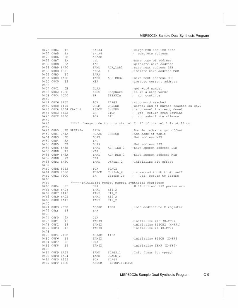
MSP50C3x Sample Dual Synthesis Program
C-9 MSP50C3x Sample Dual Synthesis Program
0426 00B4 1B SALA4 ;merge MSB and LSB into0427 00B5 1B SALA4 ; complete address0428 00B6 2C ABAAC0429 00B7 1A tab ;save copy of address0430 00B8 3A IAC ;generate next address0431 00B9 6A70 TAMD ADR_LSB2 ;save next address LSB0432 00BB 6801 AXCA 1 ;isolate next address MSB0433 00BD 15 SARA0434 00BE 6A6F TAMD ADR_MSB2 ;save next address MSB0435 00C0 12 XBA ;restore current address04360437 00C1 6B LUAA ;get word number0438 00C2 60FF ANEC StopWord ;is it a stop word?0439 00C4 40D0 BR SPEAK2a ; no, continue04400441 00C6 6262 TCX FLAGS ;stop word reached0442 00C8 6408 ORCM CH2END ;signal end of phrase reached on ch.20443 00CA 6604 ChkCh1 TSTCM CH1END ;is channel 1 already done?0444 00CC 45E2 BR STOP ; yes, return from routine0445 00CE 6E00 TCA SIL ; no, substitute silence04460447 ***** change code to turn channel 2 off if channel 1 is still on04480449 00D0 2E SPEAK2a SALA ;Double index to get offset0450 00D1 7A1A ACAAC SPEECH ;Add base of table0451 00D3 6D LUAB ;Get address MSB0452 00D4 3A IAC0453 00D5 6B LUAA ;Get address LSB0454 00D6 6A6B TAMD ADR_LSB_2 ;Save speech address LSB0455 00D8 12 XBA0456 00D9 6A6A TAMD ADR_MSB_2 ;Save speech address MSB0457 00DB 2F CLA0458 00DC 6A6C TAMD OFFSET_2 ;Initialize bit offset04590460 00DE 6262 TCX FLAGS0461 00E0 6680 TSTCM Ch2Inh_2 ;is second inhibit bit set?0462 00E2 45C0 BR ZeroKs_2b ; yes, return to ZeroKs04630464 *–––––Initialize memory mapped synthesis registers0465 00E4 2F CLA ;Kill K11 and K12 parameters0466 00E5 6A03 TAMD K11_A0467 00E7 6A13 TAMD K11_B0468 00E9 6A02 TAMD K12_A0469 00EB 6A12 TAMD K12_B04700471 00ED 7FF0 ACAAC #FF0 ;load address to X register0472 00EF 18 TAX04730474 00F0 2F CLA0475 00F1 13 TAMIX ;initialize Y1S (X=FF0)0476 00F2 13 TAMIX ;initialize PITCH2 (X=FF1)0477 00F3 13 TAMIX ;initialize Y1 (X=FF2)04780479 00F4 7162 ACAAC #1620480 00F6 13 TAMIX ;initialize PITCH (X=FF3)0481 00F7 2F CLA0482 00F8 13 TAMIX ;initialize TEMP (X=FF4)04830484 00F9 6A63 TAMD FLAGS_1 ;Init flags for speech0485 00FB 6A64 TAMD FLAGS_20486 00FD 6262 TCX FLAGS0487 00FF 65FC ANDCM ~(STOP1+STOP2)
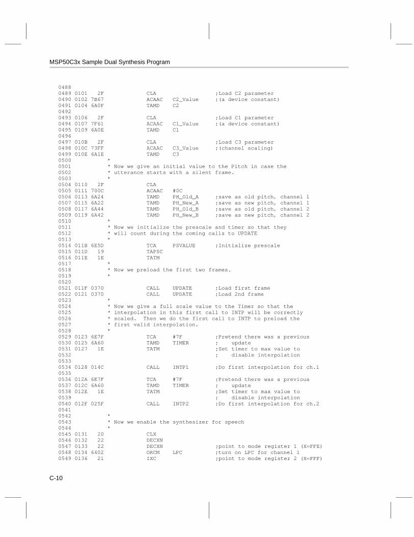
MSP50C3x Sample Dual Synthesis Program
C-10
04880489 0101 2F CLA ;Load C2 parameter0490 0102 7B67 ACAAC C2_Value ;(a device constant)0491 0104 6A0F TAMD C204920493 0106 2F CLA ;Load C1 parameter0494 0107 7F61 ACAAC C1_Value ;(a device constant)0495 0109 6A0E TAMD C104960497 010B 2F CLA ;Load C3 parameter0498 010C 73FF ACAAC C3_Value ;(channel scaling)0499 010E 6A1E TAMD C30500 *0501 * Now we give an initial value to the Pitch in case the0502 * utterance starts with a silent frame.0503 *0504 0110 2F CLA0505 0111 700C ACAAC #0C0506 0113 6A24 TAMD PH_Old_A ;save as old pitch, channel 10507 0115 6A22 TAMD PH_New_A ;save as new pitch, channel 10508 0117 6A44 TAMD PH_Old_B ;save as old pitch, channel 20509 0119 6A42 TAMD PH_New_B ;save as new pitch, channel 20510 *0511 * Now we initialize the prescale and timer so that they0512 * will count during the coming calls to UPDATE0513 *0514 011B 6E5D TCA PSVALUE ;Initialize prescale0515 011D 19 TAPSC0516 011E 1E TATM0517 *0518 * Now we preload the first two frames.0519 *05200521 011F 0370 CALL UPDATE ;Load first frame0522 0121 0370 CALL UPDATE ;Load 2nd frame0523 *0524 * Now we give a full scale value to the Timer so that the0525 * interpolation in this first call to INTP will be correctly0526 * scaled. Then we do the first call to INTP to preload the0527 * first valid interpolation.0528 *0529 0123 6E7F TCA #7F ;Pretend there was a previous0530 0125 6A60 TAMD TIMER ; update0531 0127 1E TATM ;Set timer to max value to0532 ; disable interpolation05330534 0128 014C CALL INTP1 ;Do first interpolation for ch.105350536 012A 6E7F TCA #7F ;Pretend there was a previoua0537 012C 6A60 TAMD TIMER ; update0538 012E 1E TATM ;Set timer to max value to0539 ; disable interpolation0540 012F 025F CALL INTP2 ;Do first interpolation for ch.205410542 *0543 * Now we enable the synthesizer for speech0544 *0545 0131 20 CLX0546 0132 22 DECXN0547 0133 22 DECXN ;point to mode register 1 (X=FFE)0548 0134 6402 ORCM LPC ;turn on LPC for channel 10549 0136 21 IXC ;point to mode register 2 (X=FFF)
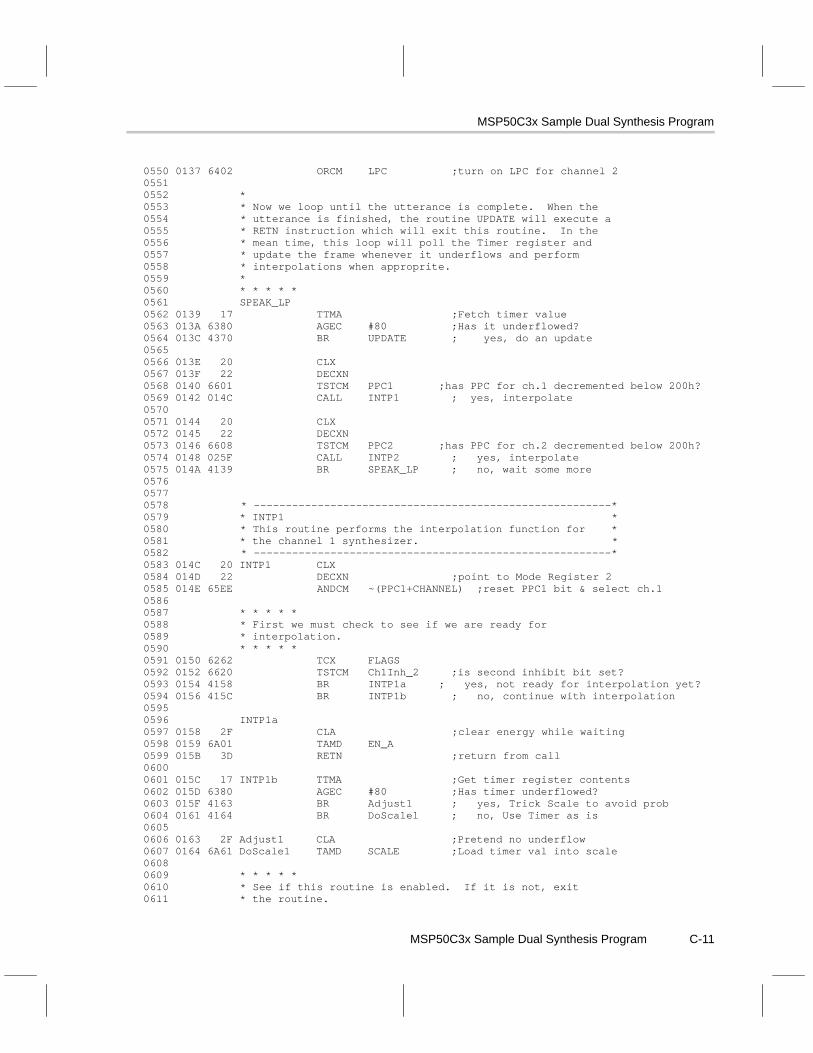
MSP50C3x Sample Dual Synthesis Program
C-11 MSP50C3x Sample Dual Synthesis Program
0550 0137 6402 ORCM LPC ;turn on LPC for channel 205510552 *0553 * Now we loop until the utterance is complete. When the0554 * utterance is finished, the routine UPDATE will execute a0555 * RETN instruction which will exit this routine. In the0556 * mean time, this loop will poll the Timer register and0557 * update the frame whenever it underflows and perform0558 * interpolations when approprite.0559 *0560 * * * * *0561 SPEAK_LP0562 0139 17 TTMA ;Fetch timer value0563 013A 6380 AGEC #80 ;Has it underflowed?0564 013C 4370 BR UPDATE ; yes, do an update05650566 013E 20 CLX0567 013F 22 DECXN0568 0140 6601 TSTCM PPC1 ;has PPC for ch.1 decremented below 200h?0569 0142 014C CALL INTP1 ; yes, interpolate05700571 0144 20 CLX0572 0145 22 DECXN0573 0146 6608 TSTCM PPC2 ;has PPC for ch.2 decremented below 200h?0574 0148 025F CALL INTP2 ; yes, interpolate0575 014A 4139 BR SPEAK_LP ; no, wait some more057605770578 * ––––––––––––––––––––––––––––––––––––––––––––––––––––––––*0579 * INTP1 *0580 * This routine performs the interpolation function for *0581 * the channel 1 synthesizer. *0582 * ––––––––––––––––––––––––––––––––––––––––––––––––––––––––*0583 014C 20 INTP1 CLX0584 014D 22 DECXN ;point to Mode Register 20585 014E 65EE ANDCM ~(PPC1+CHANNEL) ;reset PPC1 bit & select ch.105860587 * * * * *0588 * First we must check to see if we are ready for0589 * interpolation.0590 * * * * *0591 0150 6262 TCX FLAGS0592 0152 6620 TSTCM Ch1Inh_2 ;is second inhibit bit set?0593 0154 4158 BR INTP1a ; yes, not ready for interpolation yet?0594 0156 415C BR INTP1b ; no, continue with interpolation05950596 INTP1a0597 0158 2F CLA ;clear energy while waiting0598 0159 6A01 TAMD EN_A0599 015B 3D RETN ;return from call06000601 015C 17 INTP1b TTMA ;Get timer register contents0602 015D 6380 AGEC #80 ;Has timer underflowed?0603 015F 4163 BR Adjust1 ; yes, Trick Scale to avoid prob0604 0161 4164 BR DoScale1 ; no, Use Timer as is06050606 0163 2F Adjust1 CLA ;Pretend no underflow0607 0164 6A61 DoScale1 TAMD SCALE ;Load timer val into scale06080609 * * * * *0610 * See if this routine is enabled. If it is not, exit0611 * the routine.

MSP50C3x Sample Dual Synthesis Program
C-12
0612 * * * * *0613 0166 6263 TCX FLAGS_1 ;Point to channel 1 flags0614 0168 6601 TSTCM Int_Off ;If routine disabled...0615 016A 425E BR IRETN1 ; ...branch to exit point0616 * * * * *0617 * Next we need to see if the frame type has changed between0618 * voiced and unvoiced frames. If it has, we do not want to0619 * interpolate between them; we just want to use the current0620 * frame values until we have two frames of the same type to0621 * interpolate between.0622 * * * * *0623 016C 6263 TINTP1 TCX FLAGS_1 ;Point to channel 1 status flags0624 016E 6620 TSTCM Int_Inh ;Is interpolation inhibited?0625 0170 4174 BR NOINT1 ; yes, use inhibit code0626 0172 4191 BR INTPCH1 ; no, use interpolation code0627 * * * * *0628 * The following code is reached if interpolation is0629 * inhibited. It sets the stored timer value to #7F which0630 * effectively forces the interpolation to yield the old0631 * values for the working values, thus effectively disabling0632 * interpolation.0633 * * * * *0634 0174 6E7F NOINT1 TCA #7F ;Set Scale factor to0635 0176 6A61 TAMD SCALE ; highest value0636 *0637 * If the new frame has a voicing different from the last0638 * frame, we want to zero the energy until the Unvoiced bit0639 * in the mode register is changed and the K parameters are0640 * all to the correct values. We therefore check in this0641 * section of code to see if the frame voicing is different0642 * from the setting in the Mode Register. If it is, we zero0643 * the energy until after the Mode Register is modified.0644 *0645 0178 6263 TCX FLAGS_10646 017A 6680 TSTCM Unv_Flg_Old ;Is new frame unvoiced?0647 017C 4187 BR Uv1 ; yes, go to unvoiced branch06480649 017E 20 CLX0650 017F 22 DECXN ;point to Mode Register 10651 0180 22 DECXN ;New frame is voiced0652 0181 6680 TSTCM UNV ;Has mode changed to unvoiced0653 0183 418E BR ClrEN1 ; yes, clear the energy0654 0185 4191 BR INTPCH1 ; no, no action required06550656 0187 20 Uv1 CLX ;New frame is unvoiced0657 0188 22 DECXN0658 0189 22 DECXN0659 018A 6680 TSTCM UNV ;Has voicing mode changed?0660 018C 4191 BR INTPCH1 ; no, no action required06610662 018E 2F ClrEN1 CLA ;Zero Energy during update0663 018F 6A01 TAMD EN_A06640665 *0666 * Interpolate Pitch and write the result to the pitch0667 * register0668 *0669 0191 6222 INTPCH1 TCX PH_New_A ;Combine new pitch and fractional0670 0193 14 TMAIX ; pitch and leave in0671 0194 1B SALA4 ; the B register0672 0195 28 AMAAC0673 0196 21 IXC
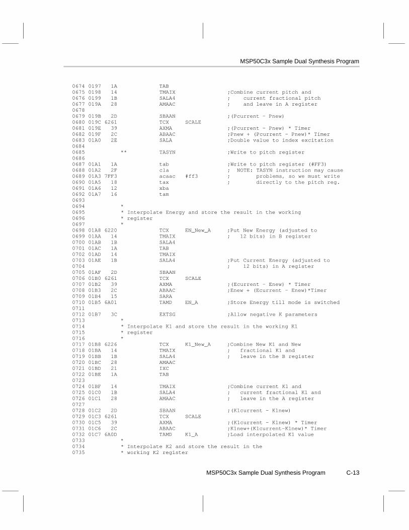
MSP50C3x Sample Dual Synthesis Program
C-13 MSP50C3x Sample Dual Synthesis Program
0674 0197 1A TAB0675 0198 14 TMAIX ;Combine current pitch and0676 0199 1B SALA4 ; current fractional pitch0677 019A 28 AMAAC ; and leave in A register06780679 019B 2D SBAAN ;(Pcurrent – Pnew)0680 019C 6261 TCX SCALE0681 019E 39 AXMA ;(Pcurrent – Pnew) * Timer0682 019F 2C ABAAC ;Pnew + (Pcurrent – Pnew)* Timer0683 01A0 2E SALA ;Double value to index excitation06840685 ** TASYN ;Write to pitch register06860687 01A1 1A tab ;Write to pitch register (#FF3)0688 01A2 2F cla ; NOTE: TASYN instruction may cause0689 01A3 7FF3 acaac #ff3 ; problems, so we must write0690 01A5 18 tax ; directly to the pitch reg.0691 01A6 12 xba0692 01A7 16 tam06930694 *0695 * Interpolate Energy and store the result in the working0696 * register0697 *0698 01A8 6220 TCX EN_New_A ;Put New Energy (adjusted to0699 01AA 14 TMAIX ; 12 bits) in B register0700 01AB 1B SALA40701 01AC 1A TAB0702 01AD 14 TMAIX0703 01AE 1B SALA4 ;Put Current Energy (adjusted to0704 ; 12 bits) in A register0705 01AF 2D SBAAN0706 01B0 6261 TCX SCALE0707 01B2 39 AXMA ;(Ecurrent – Enew) * Timer0708 01B3 2C ABAAC ;Enew + (Ecurrent – Enew)*Timer0709 01B4 15 SARA0710 01B5 6A01 TAMD EN_A ;Store Energy till mode is switched07110712 01B7 3C EXTSG ;Allow negative K parameters0713 *0714 * Interpolate K1 and store the result in the working K10715 * register0716 *0717 01B8 6226 TCX K1_New_A ;Combine New K1 and New0718 01BA 14 TMAIX ; fractional K1 and0719 01BB 1B SALA4 ; leave in the B register0720 01BC 28 AMAAC0721 01BD 21 IXC0722 01BE 1A TAB07230724 01BF 14 TMAIX ;Combine current K1 and0725 01C0 1B SALA4 ; current fractional K1 and0726 01C1 28 AMAAC ; leave in the A register07270728 01C2 2D SBAAN ;(K1current – K1new)0729 01C3 6261 TCX SCALE0730 01C5 39 AXMA ;(K1current – K1new) * Timer0731 01C6 2C ABAAC ;K1new+(K1current–K1new)* Timer0732 01C7 6A0D TAMD K1_A ;Load interpolated K1 value0733 *0734 * Interpolate K2 and store the result in the0735 * working K2 register
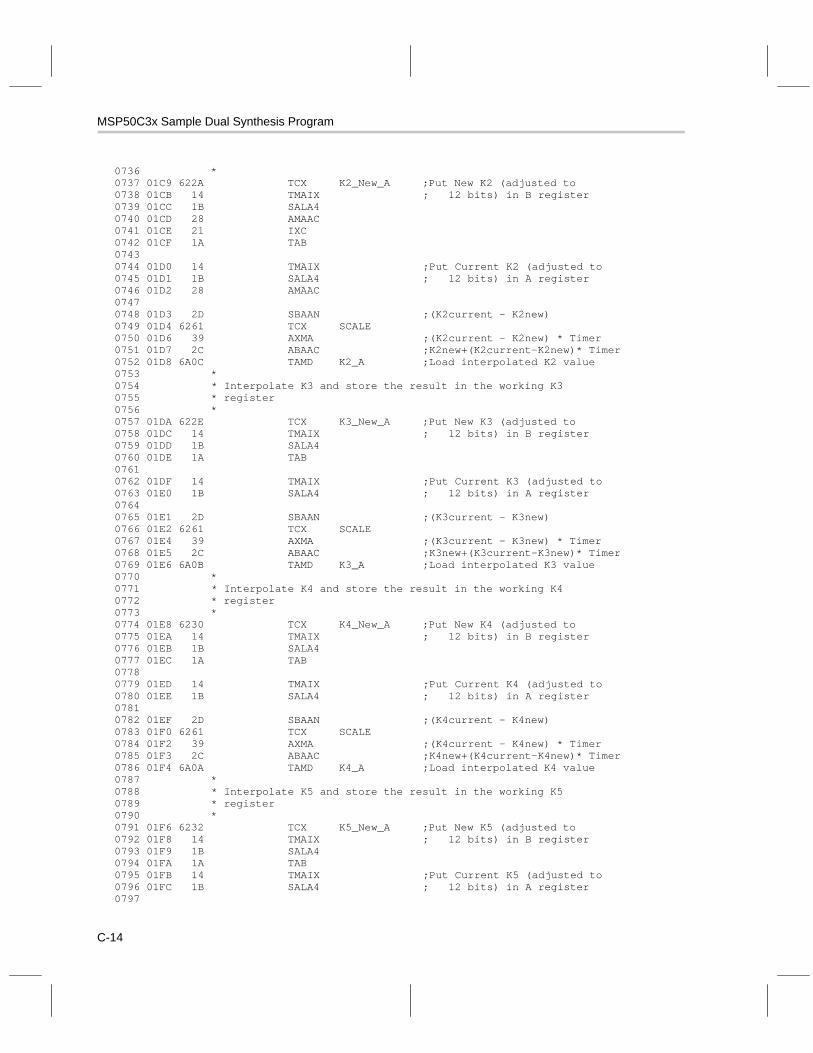
MSP50C3x Sample Dual Synthesis Program
C-14
0736 *0737 01C9 622A TCX K2_New_A ;Put New K2 (adjusted to0738 01CB 14 TMAIX ; 12 bits) in B register0739 01CC 1B SALA40740 01CD 28 AMAAC0741 01CE 21 IXC0742 01CF 1A TAB07430744 01D0 14 TMAIX ;Put Current K2 (adjusted to0745 01D1 1B SALA4 ; 12 bits) in A register0746 01D2 28 AMAAC07470748 01D3 2D SBAAN ;(K2current – K2new)0749 01D4 6261 TCX SCALE0750 01D6 39 AXMA ;(K2current – K2new) * Timer0751 01D7 2C ABAAC ;K2new+(K2current–K2new)* Timer0752 01D8 6A0C TAMD K2_A ;Load interpolated K2 value0753 *0754 * Interpolate K3 and store the result in the working K30755 * register0756 *0757 01DA 622E TCX K3_New_A ;Put New K3 (adjusted to0758 01DC 14 TMAIX ; 12 bits) in B register0759 01DD 1B SALA40760 01DE 1A TAB07610762 01DF 14 TMAIX ;Put Current K3 (adjusted to0763 01E0 1B SALA4 ; 12 bits) in A register07640765 01E1 2D SBAAN ;(K3current – K3new)0766 01E2 6261 TCX SCALE0767 01E4 39 AXMA ;(K3current – K3new) * Timer0768 01E5 2C ABAAC ;K3new+(K3current–K3new)* Timer0769 01E6 6A0B TAMD K3_A ;Load interpolated K3 value0770 *0771 * Interpolate K4 and store the result in the working K40772 * register0773 *0774 01E8 6230 TCX K4_New_A ;Put New K4 (adjusted to0775 01EA 14 TMAIX ; 12 bits) in B register0776 01EB 1B SALA40777 01EC 1A TAB07780779 01ED 14 TMAIX ;Put Current K4 (adjusted to0780 01EE 1B SALA4 ; 12 bits) in A register07810782 01EF 2D SBAAN ;(K4current – K4new)0783 01F0 6261 TCX SCALE0784 01F2 39 AXMA ;(K4current – K4new) * Timer0785 01F3 2C ABAAC ;K4new+(K4current–K4new)* Timer0786 01F4 6A0A TAMD K4_A ;Load interpolated K4 value0787 *0788 * Interpolate K5 and store the result in the working K50789 * register0790 *0791 01F6 6232 TCX K5_New_A ;Put New K5 (adjusted to0792 01F8 14 TMAIX ; 12 bits) in B register0793 01F9 1B SALA40794 01FA 1A TAB0795 01FB 14 TMAIX ;Put Current K5 (adjusted to0796 01FC 1B SALA4 ; 12 bits) in A register0797
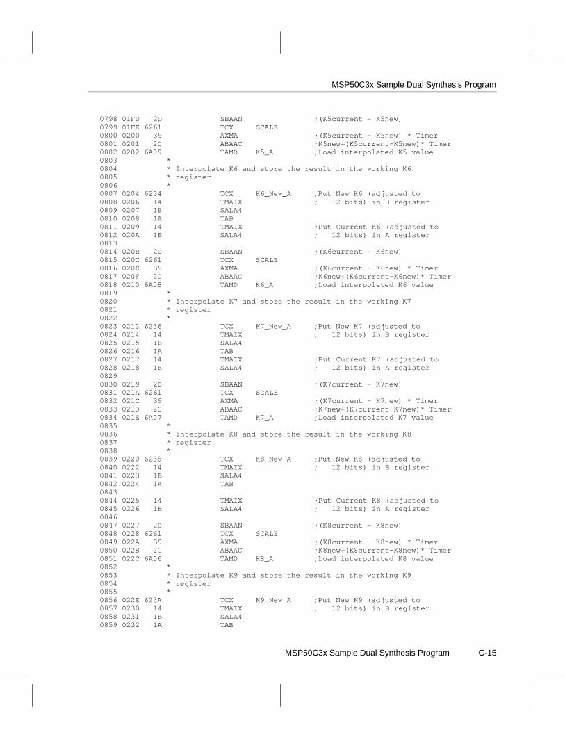
MSP50C3x Sample Dual Synthesis Program
C-15 MSP50C3x Sample Dual Synthesis Program
0798 01FD 2D SBAAN ;(K5current – K5new)0799 01FE 6261 TCX SCALE0800 0200 39 AXMA ;(K5current – K5new) * Timer0801 0201 2C ABAAC ;K5new+(K5current–K5new)* Timer0802 0202 6A09 TAMD K5_A ;Load interpolated K5 value0803 *0804 * Interpolate K6 and store the result in the working K60805 * register0806 *0807 0204 6234 TCX K6_New_A ;Put New K6 (adjusted to0808 0206 14 TMAIX ; 12 bits) in B register0809 0207 1B SALA40810 0208 1A TAB0811 0209 14 TMAIX ;Put Current K6 (adjusted to0812 020A 1B SALA4 ; 12 bits) in A register08130814 020B 2D SBAAN ;(K6current – K6new)0815 020C 6261 TCX SCALE0816 020E 39 AXMA ;(K6current – K6new) * Timer0817 020F 2C ABAAC ;K6new+(K6current–K6new)* Timer0818 0210 6A08 TAMD K6_A ;Load interpolated K6 value0819 *0820 * Interpolate K7 and store the result in the working K70821 * register0822 *0823 0212 6236 TCX K7_New_A ;Put New K7 (adjusted to0824 0214 14 TMAIX ; 12 bits) in B register0825 0215 1B SALA40826 0216 1A TAB0827 0217 14 TMAIX ;Put Current K7 (adjusted to0828 0218 1B SALA4 ; 12 bits) in A register08290830 0219 2D SBAAN ;(K7current – K7new)0831 021A 6261 TCX SCALE0832 021C 39 AXMA ;(K7current – K7new) * Timer0833 021D 2C ABAAC ;K7new+(K7current–K7new)* Timer0834 021E 6A07 TAMD K7_A ;Load interpolated K7 value0835 *0836 * Interpolate K8 and store the result in the working K80837 * register0838 *0839 0220 6238 TCX K8_New_A ;Put New K8 (adjusted to0840 0222 14 TMAIX ; 12 bits) in B register0841 0223 1B SALA40842 0224 1A TAB08430844 0225 14 TMAIX ;Put Current K8 (adjusted to0845 0226 1B SALA4 ; 12 bits) in A register08460847 0227 2D SBAAN ;(K8current – K8new)0848 0228 6261 TCX SCALE0849 022A 39 AXMA ;(K8current – K8new) * Timer0850 022B 2C ABAAC ;K8new+(K8current–K8new)* Timer0851 022C 6A06 TAMD K8_A ;Load interpolated K8 value0852 *0853 * Interpolate K9 and store the result in the working K90854 * register0855 *0856 022E 623A TCX K9_New_A ;Put New K9 (adjusted to0857 0230 14 TMAIX ; 12 bits) in B register0858 0231 1B SALA40859 0232 1A TAB
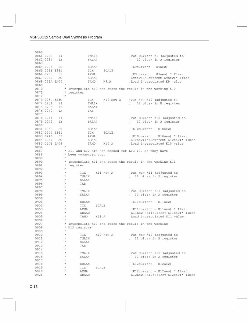
MSP50C3x Sample Dual Synthesis Program
C-16
08600861 0233 14 TMAIX ;Put Current K9 (adjusted to0862 0234 1B SALA4 ; 12 bits) in A register08630864 0235 2D SBAAN ;(K9current – K9new)0865 0236 6261 TCX SCALE0866 0238 39 AXMA ;(K9current – K9new) * Timer0867 0239 2C ABAAC ;K9new+(K9current–K9new)* Timer0868 023A 6A05 TAMD K9_A ;Load interpolated K9 value0869 *0870 * Interpolate K10 and store the result in the working K100871 * register0872 *0873 023C 623C TCX K10_New_A ;Put New K10 (adjusted to0874 023E 14 TMAIX ; 12 bits) in B register0875 023F 1B SALA40876 0240 1A TAB08770878 0241 14 TMAIX ;Put Current K10 (adjusted to0879 0242 1B SALA4 ; 12 bits) in A register08800881 0243 2D SBAAN ;(K10current – K10new)0882 0244 6261 TCX SCALE0883 0246 39 AXMA ;(K10current – K10new) * Timer0884 0247 2C ABAAC ;K10new+(K10current–K10new)* Timer0885 0248 6A04 TAMD K10_A ;Load interpolated K10 value0886 *0887 * K11 and K12 are not needed for LPC 10, so they have0888 * been commented out.0889 *0890 * Interpolate K11 and store the result in the working K110891 * register0892 *0893 * TCX K11_New_A ;Put New K11 (adjusted to0894 * TMAIX ; 12 bits) in B register0895 * SALA40896 * TAB0897 *0898 * TMAIX ;Put Current K11 (adjusted to0899 * SALA4 ; 12 bits) in A register0900 *0901 * SBAAN ;(K11current – K11new)0902 * TCX SCALE0903 * AXMA ;(K11current – K11new) * Timer0904 * ABAAC ;K11new+(K11current–K11new)* Timer0905 * TAMD K11_A ;Load interpolated K11 value0906 *0907 * Interpolate K12 and store the result in the working0908 * K12 register0909 *0910 * TCX K12_New_A ;Put New K12 (adjusted to0911 * TMAIX ; 12 bits) in B register0912 * SALA40913 * TAB0914 *0915 * TMAIX ;Put Current K12 (adjusted to0916 * SALA4 ; 12 bits) in A register0917 *0918 * SBAAN ;(K12current – K12new)0919 * TCX SCALE0920 * AXMA ;(K12current – K12new) * Timer0921 * ABAAC ;K12new+(K12current–K12new)* Timer
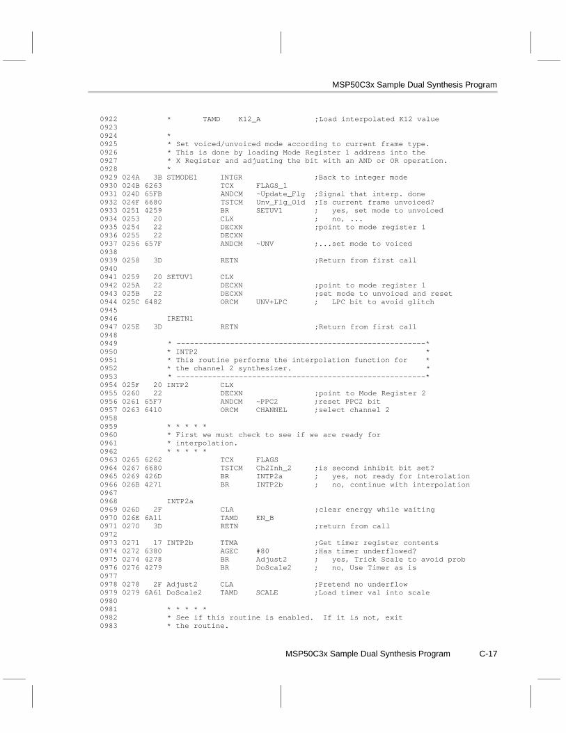
MSP50C3x Sample Dual Synthesis Program
C-17 MSP50C3x Sample Dual Synthesis Program
0922 * TAMD K12_A ;Load interpolated K12 value09230924 *0925 * Set voiced/unvoiced mode according to current frame type.0926 * This is done by loading Mode Register 1 address into the0927 * X Register and adjusting the bit with an AND or OR operation.0928 *0929 024A 3B STMODE1 INTGR ;Back to integer mode0930 024B 6263 TCX FLAGS_10931 024D 65FB ANDCM ~Update_Flg ;Signal that interp. done0932 024F 6680 TSTCM Unv_Flg_Old ;Is current frame unvoiced?0933 0251 4259 BR SETUV1 ; yes, set mode to unvoiced0934 0253 20 CLX ; no, ...0935 0254 22 DECXN ;point to mode register 10936 0255 22 DECXN0937 0256 657F ANDCM ~UNV ;...set mode to voiced09380939 0258 3D RETN ;Return from first call09400941 0259 20 SETUV1 CLX0942 025A 22 DECXN ;point to mode register 10943 025B 22 DECXN ;set mode to unvoiced and reset0944 025C 6482 ORCM UNV+LPC ; LPC bit to avoid glitch09450946 IRETN10947 025E 3D RETN ;Return from first call09480949 * ––––––––––––––––––––––––––––––––––––––––––––––––––––––––*0950 * INTP2 *0951 * This routine performs the interpolation function for *0952 * the channel 2 synthesizer. *0953 * ––––––––––––––––––––––––––––––––––––––––––––––––––––––––*0954 025F 20 INTP2 CLX0955 0260 22 DECXN ;point to Mode Register 20956 0261 65F7 ANDCM ~PPC2 ;reset PPC2 bit0957 0263 6410 ORCM CHANNEL ;select channel 209580959 * * * * *0960 * First we must check to see if we are ready for0961 * interpolation.0962 * * * * *0963 0265 6262 TCX FLAGS0964 0267 6680 TSTCM Ch2Inh_2 ;is second inhibit bit set?0965 0269 426D BR INTP2a ; yes, not ready for interolation0966 026B 4271 BR INTP2b ; no, continue with interpolation09670968 INTP2a0969 026D 2F CLA ;clear energy while waiting0970 026E 6A11 TAMD EN_B0971 0270 3D RETN ;return from call09720973 0271 17 INTP2b TTMA ;Get timer register contents0974 0272 6380 AGEC #80 ;Has timer underflowed?0975 0274 4278 BR Adjust2 ; yes, Trick Scale to avoid prob0976 0276 4279 BR DoScale2 ; no, Use Timer as is09770978 0278 2F Adjust2 CLA ;Pretend no underflow0979 0279 6A61 DoScale2 TAMD SCALE ;Load timer val into scale09800981 * * * * *0982 * See if this routine is enabled. If it is not, exit0983 * the routine.

MSP50C3x Sample Dual Synthesis Program
C-18
0984 * * * * *0985 027B 6264 TCX FLAGS_2 ;Point to channel 2 flags0986 027D 6601 TSTCM Int_Off ;If routine disabled...0987 027F 436F BR IRETN2 ; ...branch to exit point0988 * * * * *0989 * Next we need to see if the frame type has changed between0990 * voiced and unvoiced frames. If it has, we do not want to0991 * interpolate between them; we just want to use the current0992 * frame values until we have two frames of the same type to0993 * interpolate between.0994 * * * * *0995 0281 6264 TINTP2 TCX FLAGS_2 ;Point to status flags0996 0283 6620 TSTCM Int_Inh ;Is interpolation inhibited?0997 0285 4289 BR NOINT2 ; yes, use inhibit code0998 0287 42A4 BR INTPCH2 ; no, use interpolation code0999 * * * * *1000 * The following code is reached if interpolation is1001 * inhibited. It sets the stored timer value to #7F which1002 * effectively forces the interpolation to yield the old1003 * values for the working values, thus effectively disabling1004 * interpolation.1005 * * * * *1006 0289 6E7F NOINT2 TCA #7F ;Set Scale factor to1007 028B 6A61 TAMD SCALE ; highest value1008 *1009 * If the new frame has a voicing different from the last1010 * frame, we want to zero the energy until the Unvoiced bit1011 * in the mode register is changed and the K parameters are1012 * all to the correct values. We therefore check in this1013 * section of code to see if the frame voicing is different1014 * from the setting in the Mode Register. If it is, we zero1015 * the energy until after the Mode Register is modified.1016 *1017 028D 6264 TCX FLAGS_21018 028F 6680 TSTCM Unv_Flg_Old ;Is new frame unvoiced?1019 0291 429B BR Uv2 ; yes, go to unvoiced branch10201021 0293 20 CLX1022 0294 22 DECXN ;point to mode register 21023 0295 6680 TSTCM UNV ;Has mode changed to unvoiced?1024 0297 42A1 BR ClrEN2 ; yes, clear the energy1025 0299 42A4 BR INTPCH2 ; no, no action required10261027 029B 20 Uv2 CLX ;New frame is unvoiced1028 029C 22 DECXN ;point to mode register 21029 029D 6680 TSTCM UNV ;Has voicing mode changed?1030 029F 42A4 BR INTPCH2 ; no, no action required10311032 02A1 2F ClrEN2 CLA ;Zero Energy during update1033 02A2 6A11 TAMD EN_B10341035 *1036 * Interpolate Pitch and write the result to the pitch1037 * register1038 *1039 02A4 6242 INTPCH2 TCX PH_New_B ;Combine new pitch and fractional1040 02A6 14 TMAIX ; pitch and leave in1041 02A7 1B SALA4 ; the B register1042 02A8 28 AMAAC1043 02A9 21 IXC1044 02AA 1A TAB1045 02AB 14 TMAIX ;Combine current pitch and
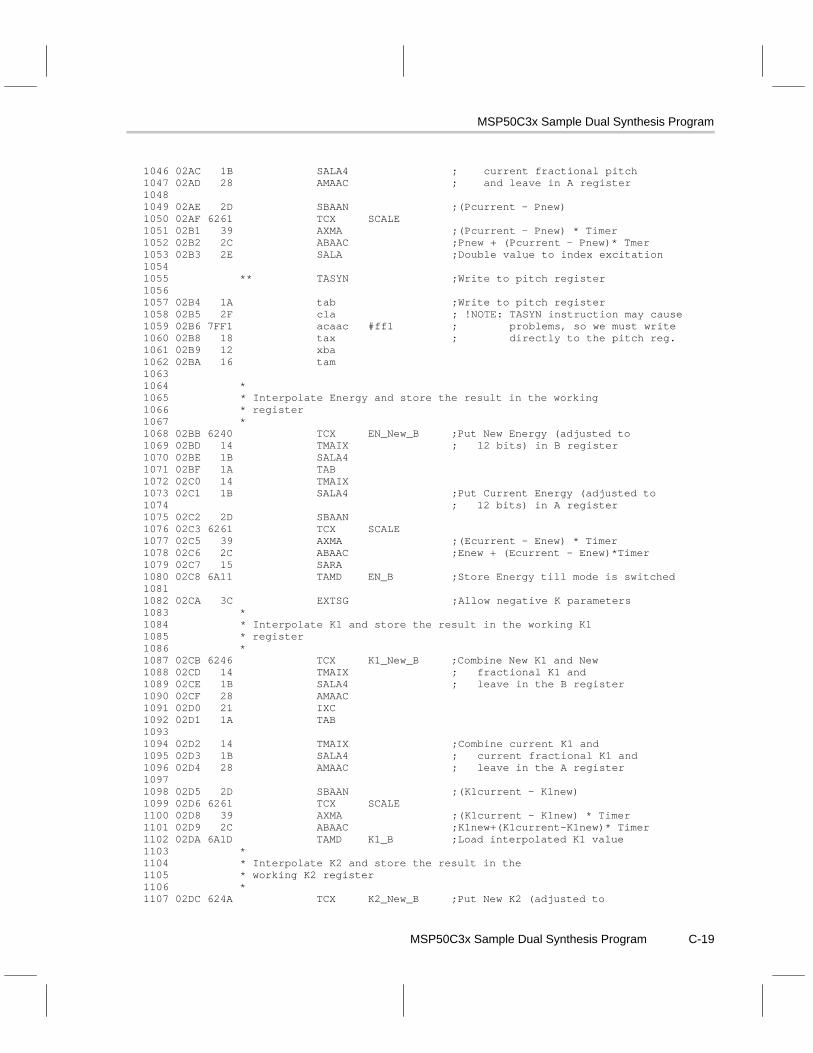
MSP50C3x Sample Dual Synthesis Program
C-19 MSP50C3x Sample Dual Synthesis Program
1046 02AC 1B SALA4 ; current fractional pitch1047 02AD 28 AMAAC ; and leave in A register10481049 02AE 2D SBAAN ;(Pcurrent – Pnew)1050 02AF 6261 TCX SCALE1051 02B1 39 AXMA ;(Pcurrent – Pnew) * Timer1052 02B2 2C ABAAC ;Pnew + (Pcurrent – Pnew)* Tmer1053 02B3 2E SALA ;Double value to index excitation10541055 ** TASYN ;Write to pitch register10561057 02B4 1A tab ;Write to pitch register1058 02B5 2F cla ; !NOTE: TASYN instruction may cause1059 02B6 7FF1 acaac #ff1 ; problems, so we must write1060 02B8 18 tax ; directly to the pitch reg.1061 02B9 12 xba1062 02BA 16 tam10631064 *1065 * Interpolate Energy and store the result in the working1066 * register1067 *1068 02BB 6240 TCX EN_New_B ;Put New Energy (adjusted to1069 02BD 14 TMAIX ; 12 bits) in B register1070 02BE 1B SALA41071 02BF 1A TAB1072 02C0 14 TMAIX1073 02C1 1B SALA4 ;Put Current Energy (adjusted to1074 ; 12 bits) in A register1075 02C2 2D SBAAN1076 02C3 6261 TCX SCALE1077 02C5 39 AXMA ;(Ecurrent – Enew) * Timer1078 02C6 2C ABAAC ;Enew + (Ecurrent – Enew)*Timer1079 02C7 15 SARA1080 02C8 6A11 TAMD EN_B ;Store Energy till mode is switched10811082 02CA 3C EXTSG ;Allow negative K parameters1083 *1084 * Interpolate K1 and store the result in the working K11085 * register1086 *1087 02CB 6246 TCX K1_New_B ;Combine New K1 and New1088 02CD 14 TMAIX ; fractional K1 and1089 02CE 1B SALA4 ; leave in the B register1090 02CF 28 AMAAC1091 02D0 21 IXC1092 02D1 1A TAB10931094 02D2 14 TMAIX ;Combine current K1 and1095 02D3 1B SALA4 ; current fractional K1 and1096 02D4 28 AMAAC ; leave in the A register10971098 02D5 2D SBAAN ;(K1current – K1new)1099 02D6 6261 TCX SCALE1100 02D8 39 AXMA ;(K1current – K1new) * Timer1101 02D9 2C ABAAC ;K1new+(K1current–K1new)* Timer1102 02DA 6A1D TAMD K1_B ;Load interpolated K1 value1103 *1104 * Interpolate K2 and store the result in the1105 * working K2 register1106 *1107 02DC 624A TCX K2_New_B ;Put New K2 (adjusted to
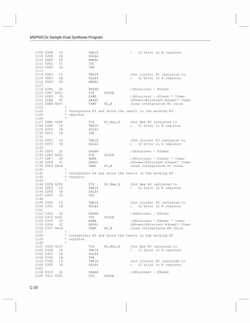
MSP50C3x Sample Dual Synthesis Program
C-20
1108 02DE 14 TMAIX ; 12 bits) in B register1109 02DF 1B SALA41110 02E0 28 AMAAC1111 02E1 21 IXC1112 02E2 1A TAB11131114 02E3 14 TMAIX ;Put Current K2 (adjusted to1115 02E4 1B SALA4 ; 12 bits) in A register1116 02E5 28 AMAAC11171118 02E6 2D SBAAN ;(K2current – K2new)1119 02E7 6261 TCX SCALE1120 02E9 39 AXMA ;(K2current – K2new) * Timer1121 02EA 2C ABAAC ;K2new+(K2current–K2new)* Timer1122 02EB 6A1C TAMD K2_B ;Load interpolated K2 value1123 *1124 * Interpolate K3 and store the result in the working K31125 * register1126 *1127 02ED 624E TCX K3_New_B ;Put New K3 (adjusted to1128 02EF 14 TMAIX ; 12 bits) in B register1129 02F0 1B SALA41130 02F1 1A TAB11311132 02F2 14 TMAIX ;Put Current K3 (adjusted to1133 02F3 1B SALA4 ; 12 bits) in A register11341135 02F4 2D SBAAN ;(K3current – K3new)1136 02F5 6261 TCX SCALE1137 02F7 39 AXMA ;(K3current – K3new) * Timer1138 02F8 2C ABAAC ;K3new+(K3current–K3new)* Timer1139 02F9 6A1B TAMD K3_B ;Load interpolated K3 value1140 *1141 * Interpolate K4 and store the result in the working K41142 * register1143 *1144 02FB 6250 TCX K4_New_B ;Put New K4 (adjusted to1145 02FD 14 TMAIX ; 12 bits) in B register1146 02FE 1B SALA41147 02FF 1A TAB11481149 0300 14 TMAIX ;Put Current K4 (adjusted to1150 0301 1B SALA4 ; 12 bits) in A register11511152 0302 2D SBAAN ;(K4current – K4new)1153 0303 6261 TCX SCALE1154 0305 39 AXMA ;(K4current – K4new) * Timer1155 0306 2C ABAAC ;K4new+(K4current–K4new)* Timer1156 0307 6A1A TAMD K4_B ;Load interpolated K4 value1157 *1158 * Interpolate K5 and store the result in the working K51159 * register1160 *1161 0309 6252 TCX K5_New_B ;Put New K5 (adjusted to1162 030B 14 TMAIX ; 12 bits) in B register1163 030C 1B SALA41164 030D 1A TAB1165 030E 14 TMAIX ;Put Current K5 (adjusted to1166 030F 1B SALA4 ; 12 bits) in A register11671168 0310 2D SBAAN ;(K5current – K5new)1169 0311 6261 TCX SCALE
MSP50C3x Sample Dual Synthesis Program
C-21 MSP50C3x Sample Dual Synthesis Program
1170 0313 39 AXMA ;(K5current – K5new) * Timer1171 0314 2C ABAAC ;K5new+(K5current–K5new)* Timer1172 0315 6A19 TAMD K5_B ;Load interpolated K5 value1173 *1174 * Interpolate K6 and store the result in the working K61175 * register1176 *1177 0317 6254 TCX K6_New_B ;Put New K6 (adjusted to1178 0319 14 TMAIX ; 12 bits) in B register1179 031A 1B SALA41180 031B 1A TAB1181 031C 14 TMAIX ;Put Current K6 (adjusted to1182 031D 1B SALA4 ; 12 bits) in A register11831184 031E 2D SBAAN ;(K6current – K6new)1185 031F 6261 TCX SCALE1186 0321 39 AXMA ;(K6current – K6new) * Timer1187 0322 2C ABAAC ;K6new+(K6current–K6new)* Timer1188 0323 6A18 TAMD K6_B ;Load interpolated K6 value1189 *1190 * Interpolate K7 and store the result in the working K71191 * register1192 *1193 0325 6256 TCX K7_New_B ;Put New K7 (adjusted to1194 0327 14 TMAIX ; 12 bits) in B register1195 0328 1B SALA41196 0329 1A TAB1197 032A 14 TMAIX ;Put Current K7 (adjusted to1198 032B 1B SALA4 ; 12 bits) in A register11991200 032C 2D SBAAN ;(K7current – K7new)1201 032D 6261 TCX SCALE1202 032F 39 AXMA ;(K7current – K7new) * Timer1203 0330 2C ABAAC ;K7new+(K7current–K7new)* Timer1204 0331 6A17 TAMD K7_B ;Load interpolated K7 value1205 *1206 * Interpolate K8 and store the result in the working K81207 * register1208 *1209 0333 6258 TCX K8_New_B ;Put New K8 (adjusted to1210 0335 14 TMAIX ; 12 bits) in B register1211 0336 1B SALA41212 0337 1A TAB12131214 0338 14 TMAIX ;Put Current K8 (adjusted to1215 0339 1B SALA4 ; 12 bits) in A register12161217 033A 2D SBAAN ;(K8current – K8new)1218 033B 6261 TCX SCALE1219 033D 39 AXMA ;(K8current – K8new) * Timer1220 033E 2C ABAAC ;K8new+(K8current–K8new)* Timer1221 033F 6A16 TAMD K8_B ;Load interpolated K8 value1222 *1223 * Interpolate K9 and store the result in the working K91224 * register1225 *1226 0341 625A TCX K9_New_B ;Put New K9 (adjusted to1227 0343 14 TMAIX ; 12 bits) in B register1228 0344 1B SALA41229 0345 1A TAB12301231 0346 14 TMAIX ;Put Current K9 (adjusted to
MSP50C3x Sample Dual Synthesis Program
C-22
1232 0347 1B SALA4 ; 12 bits) in A register12331234 0348 2D SBAAN ;(K9current – K9new)1235 0349 6261 TCX SCALE1236 034B 39 AXMA ;(K9current – K9new) * Timer1237 034C 2C ABAAC ;K9new+(K9current–K9new)* Timer1238 034D 6A15 TAMD K9_B ;Load interpolated K9 value1239 *1240 * Interpolate K10 and store the result in the working K101241 * register1242 *1243 034F 625C TCX K10_New_B ;Put New K10 (adjusted to1244 0351 14 TMAIX ; 12 bits) in B register1245 0352 1B SALA41246 0353 1A TAB12471248 0354 14 TMAIX ;Put Current K10 (adjusted to1249 0355 1B SALA4 ; 12 bits) in A register12501251 0356 2D SBAAN ;(K10current – K10new)1252 0357 6261 TCX SCALE1253 0359 39 AXMA ;(K10current – K10new) * Timer1254 035A 2C ABAAC ;K10new+(K10current–K10new)* Timer1255 035B 6A14 TAMD K10_B ;Load interpolated K10 value1256 *1257 * K11 and K12 are not needed for LPC 10, so they have1258 * been commented out.1259 *1260 * Interpolate K11 and store the result in the working K111261 * register1262 *1263 * TCX K11_New_B ;Put New K11 (adjusted to1264 * TMAIX ; 12 bits) in B register1265 * SALA41266 * TAB12671268 * TMAIX ;Put Current K11 (adjusted to1269 * SALA4 ; 12 bits) in A register12701271 * SBAAN ;(K11current – K11new)1272 * TCX SCALE1273 * AXMA ;(K11current – K11new) * Timer1274 * ABAAC ;K11new+(K11current–K11new)* Timer1275 * TAMD K11_B ;Load interpolated K11 value1276 *1277 * Interpolate K12 and store the result in the working1278 * K12 register1279 *1280 * TCX K12_New_B ;Put New K12 (adjusted to1281 * TMAIX ; 12 bits) in B register1282 * SALA41283 * TAB12841285 * TMAIX ;Put Current K12 (adjusted to1286 * SALA4 ; 12 bits) in A register12871288 * SBAAN ;(K12current – K12new)1289 * TCX SCALE1290 * AXMA ;(K12current – K12new) * Timer1291 * ABAAC ;K12new+(K12current–K12new)* Timer1292 * TAMD K12_B ;Load interpolated K12 value1293 *
MSP50C3x Sample Dual Synthesis Program
C-23 MSP50C3x Sample Dual Synthesis Program
1294 * Set voiced/unvoiced mode according to current frame type.1295 * This is done by loading Mode Register 2 address into the1296 * X Register and adjusting the bit with an AND or OR operation.1297 *1298 035D 3B STMODE2 INTGR ;Back to integer mode1299 035E 6264 TCX FLAGS_21300 0360 65FB ANDCM ~Update_Flg ;Signal that interp done1301 0362 6680 TSTCM Unv_Flg_Old ;Is current frame unvoiced?1302 0364 436B BR SETUV2 ; yes, set mode to unvoiced1303 0366 20 CLX ; no, ...1304 0367 22 DECXN ;point to mode register 21305 0368 657F ANDCM ~UNV ;...set mode to voiced13061307 036A 3D RETN ;Return from first call13081309 036B 20 SETUV2 CLX1310 036C 22 DECXN ;point to mode register 21311 036D 6480 ORCM UNV ;Current frame is unvoiced, so1312 ; set mode to unvoiced.1313 IRETN21314 036F 3D RETN ;Return from first call1315131613171318 * * * * *1319 * Update the parameters for a new frame – CHANNEL 11320 * * * * *1321 * * * * *1322 * To prevent double updates, if the stored value of the1323 * timer register is zero, then we need to change it to #7F.1324 * If we do not do this, then the polling routine will1325 * discover an underflow and call Update a second time.1326 * We also need to check if inhibit bits are set (if new1327 * word has just been started) because two frames need to1328 * be pre–loaded before interpolation can happen.1329 * * * * *1330 0370 6260 UPDATE TCX TIMER ;Get stored value1331 0372 11 TMA ; of Timer into A13321333 0373 6000 ANEC 0 ;Is it zero?1334 0375 437A BR UPDT00a ; no, do nothing1335 0377 6E7F TCA #7F ; yes, replace value1336 0379 16 TAM13371338 037A 6262 UPDT00a TCX FLAGS1339 037C 6610 TSTCM Ch1Inh_1 ;is the first inhibit bit set?1340 037E 4382 BR UPDT00b ; yes, clear it1341 0380 4386 BR UPDT00c ; no, test second bit13421343 0382 65EF UPDT00b ANDCM ~Ch1Inh_1 ;clear first inhibit bit1344 0384 438E BR UPDT0013451346 0386 6620 UPDT00c TSTCM Ch1Inh_2 ;is the second inhibit bit set?1347 0388 438C BR UPDT00d ; yes, clear it1348 038A 438E BR UPDT00 ; no, continue with update13491350 038C 65DF UPDT00d ANDCM ~Ch1Inh_2 ;clear second inhibit bit135113521353 * * * * *1354 * First we need to test to see if a stop frame was1355 * encountered on the last pass through the routine. If the
MSP50C3x Sample Dual Synthesis Program
C-24
1356 * previous frame was a stop frame, we need to turn off the1357 * synthesizer and stop speaking.1358 * * * * *1359 038E 6601 UPDT00 TSTCM STOP1 ;Was stop frame encountered1360 0390 4476 BR ZeroKs_1a ; yes, zero channel 1 K parameters13611362 * * * * *1363 * Transfer the state of the previous frame to the Unvoiced1364 * flag (Current).1365 * * * * *1366 0392 6263 UPDT01 TCX FLAGS_1 ;Point to channel 1 flags1367 0394 061E CALL XFER_FLAGS ; and xfer ”new” to ”old”1368 * * * * *1369 * Transfer the new frame parameters into the1370 * storage location used for the old frame parameters.1371 * * * * *1372 0396 6220 TCX EN_New_A ;Point to ch. 1 data1373 0398 06EF CALL XFER_PARMS ; and transfer parameters1374 * * * * *1375 * Turn on channel 1 and load address to speech1376 * address register1377 * * * * *1378 039A 0717 CALL INIT113791380 * * * * *1381 * We have now discarded the ”old” values by replacing1382 * them with the ”new” values. We now need to read in1383 * another frame of speech data and use them as the1384 * new ”new” values.1385 * * * * *1386 *––––– ENERGY –––––1387 039C 6263 TCX FLAGS_1 ;point to channel 1 flags1388 039E 6E04 TCA EBITS1389 03A0 0635 CALL C1GETN ;Get coded energy1390 03A2 6000 ANEC ESILENCE ;Is it a silent frame?1391 03A4 43AC BR UPDT0 ; No, continue1392 03A6 6263 TCX FLAGS_11393 03A8 6408 ORCM Sil_Flg_New ; Yes, set silence flag1394 03AA 4491 BR ZeroKs_1 ; and zero K params13951396 03AC 600F UPDT0 ANEC ESTOP ;Is it a stop frame?1397 03AE 43BA BR UPDT1 ; no, continue1398 03B0 6263 TCX FLAGS_11399 03B2 6408 ORCM Sil_Flg_New ;yes, set flags1400 03B4 6262 tcx flags1401 03B6 6401 orcm stop1 ;signal stop frame reached on ch.11402 03B8 4491 BR ZeroKs_1 ; and zero K params14031404 03BA 7751 UPDT1 ACAAC TBLEN ;Add table offset to energy1405 03BC 6B LUAA ;Get decoded energy1406 03BD 6A20 TAMD EN_New_A ;Store the Energy in RAM1407 * * * * *1408 * If this is a silent frame, we are done with the Update1409 * for channel 1, skip to the Update for channel 2. If1410 * the previous frame was silent, the new frame should be1411 * spoken immediately with no ramp up due to interpolation.1412 * * * * *1413 03BF 6263 TCX FLAGS_11414 03C1 6608 TSTCM Sil_Flg_New ;Is this a silent frame?1415 03C3 44AD BR Update_2 ; yes, go to channel 2 update1416 * * * * *1417 * A repeat frame will use the K parameters from the previous
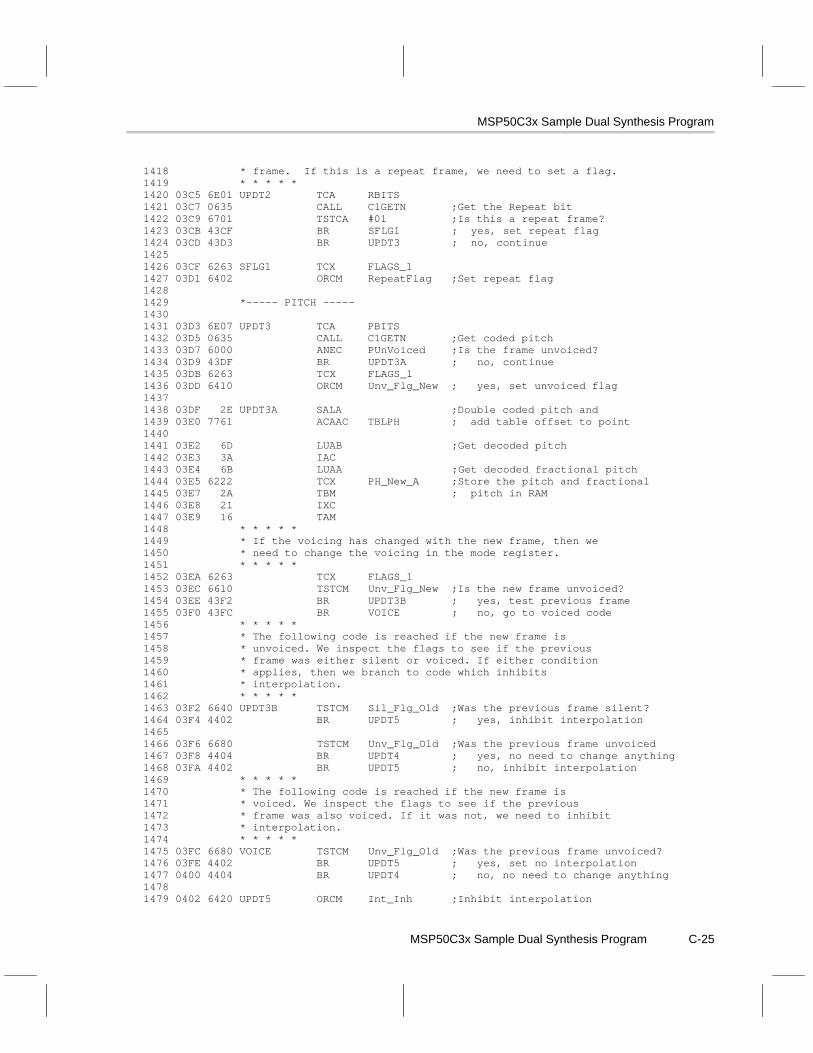
MSP50C3x Sample Dual Synthesis Program
C-25 MSP50C3x Sample Dual Synthesis Program
1418 * frame. If this is a repeat frame, we need to set a flag.1419 * * * * *1420 03C5 6E01 UPDT2 TCA RBITS1421 03C7 0635 CALL C1GETN ;Get the Repeat bit1422 03C9 6701 TSTCA #01 ;Is this a repeat frame?1423 03CB 43CF BR SFLG1 ; yes, set repeat flag1424 03CD 43D3 BR UPDT3 ; no, continue14251426 03CF 6263 SFLG1 TCX FLAGS_11427 03D1 6402 ORCM RepeatFlag ;Set repeat flag14281429 *––––– PITCH –––––14301431 03D3 6E07 UPDT3 TCA PBITS1432 03D5 0635 CALL C1GETN ;Get coded pitch1433 03D7 6000 ANEC PUnVoiced ;Is the frame unvoiced?1434 03D9 43DF BR UPDT3A ; no, continue1435 03DB 6263 TCX FLAGS_11436 03DD 6410 ORCM Unv_Flg_New ; yes, set unvoiced flag14371438 03DF 2E UPDT3A SALA ;Double coded pitch and1439 03E0 7761 ACAAC TBLPH ; add table offset to point14401441 03E2 6D LUAB ;Get decoded pitch1442 03E3 3A IAC1443 03E4 6B LUAA ;Get decoded fractional pitch1444 03E5 6222 TCX PH_New_A ;Store the pitch and fractional1445 03E7 2A TBM ; pitch in RAM1446 03E8 21 IXC1447 03E9 16 TAM1448 * * * * *1449 * If the voicing has changed with the new frame, then we1450 * need to change the voicing in the mode register.1451 * * * * *1452 03EA 6263 TCX FLAGS_11453 03EC 6610 TSTCM Unv_Flg_New ;Is the new frame unvoiced?1454 03EE 43F2 BR UPDT3B ; yes, test previous frame1455 03F0 43FC BR VOICE ; no, go to voiced code1456 * * * * *1457 * The following code is reached if the new frame is1458 * unvoiced. We inspect the flags to see if the previous1459 * frame was either silent or voiced. If either condition1460 * applies, then we branch to code which inhibits1461 * interpolation.1462 * * * * *1463 03F2 6640 UPDT3B TSTCM Sil_Flg_Old ;Was the previous frame silent?1464 03F4 4402 BR UPDT5 ; yes, inhibit interpolation14651466 03F6 6680 TSTCM Unv_Flg_Old ;Was the previous frame unvoiced1467 03F8 4404 BR UPDT4 ; yes, no need to change anything1468 03FA 4402 BR UPDT5 ; no, inhibit interpolation1469 * * * * *1470 * The following code is reached if the new frame is1471 * voiced. We inspect the flags to see if the previous1472 * frame was also voiced. If it was not, we need to inhibit1473 * interpolation.1474 * * * * *1475 03FC 6680 VOICE TSTCM Unv_Flg_Old ;Was the previous frame unvoiced?1476 03FE 4402 BR UPDT5 ; yes, set no interpolation1477 0400 4404 BR UPDT4 ; no, no need to change anything14781479 0402 6420 UPDT5 ORCM Int_Inh ;Inhibit interpolation
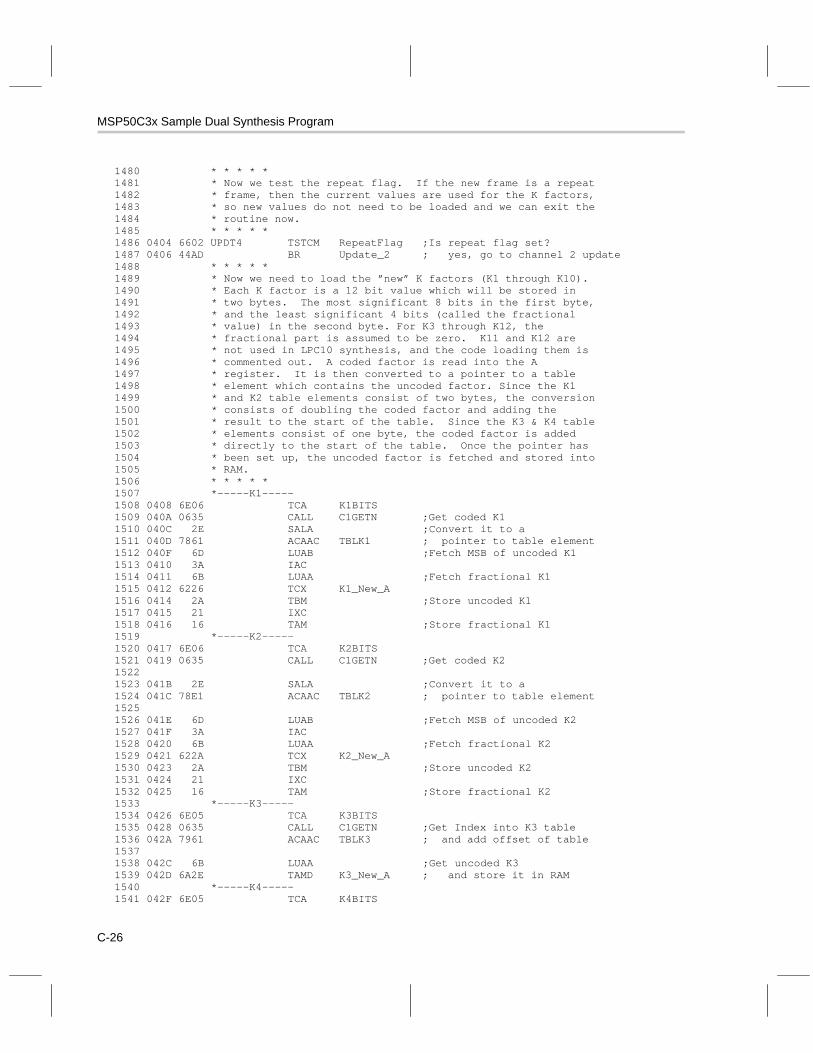
MSP50C3x Sample Dual Synthesis Program
C-26
1480 * * * * *1481 * Now we test the repeat flag. If the new frame is a repeat1482 * frame, then the current values are used for the K factors,1483 * so new values do not need to be loaded and we can exit the1484 * routine now.1485 * * * * *1486 0404 6602 UPDT4 TSTCM RepeatFlag ;Is repeat flag set?1487 0406 44AD BR Update_2 ; yes, go to channel 2 update1488 * * * * *1489 * Now we need to load the ”new” K factors (K1 through K10).1490 * Each K factor is a 12 bit value which will be stored in1491 * two bytes. The most significant 8 bits in the first byte,1492 * and the least significant 4 bits (called the fractional1493 * value) in the second byte. For K3 through K12, the1494 * fractional part is assumed to be zero. K11 and K12 are1495 * not used in LPC10 synthesis, and the code loading them is1496 * commented out. A coded factor is read into the A1497 * register. It is then converted to a pointer to a table1498 * element which contains the uncoded factor. Since the K11499 * and K2 table elements consist of two bytes, the conversion1500 * consists of doubling the coded factor and adding the1501 * result to the start of the table. Since the K3 & K4 table1502 * elements consist of one byte, the coded factor is added1503 * directly to the start of the table. Once the pointer has1504 * been set up, the uncoded factor is fetched and stored into1505 * RAM.1506 * * * * *1507 *–––––K1–––––1508 0408 6E06 TCA K1BITS1509 040A 0635 CALL C1GETN ;Get coded K11510 040C 2E SALA ;Convert it to a1511 040D 7861 ACAAC TBLK1 ; pointer to table element1512 040F 6D LUAB ;Fetch MSB of uncoded K11513 0410 3A IAC1514 0411 6B LUAA ;Fetch fractional K11515 0412 6226 TCX K1_New_A1516 0414 2A TBM ;Store uncoded K11517 0415 21 IXC1518 0416 16 TAM ;Store fractional K11519 *–––––K2–––––1520 0417 6E06 TCA K2BITS1521 0419 0635 CALL C1GETN ;Get coded K215221523 041B 2E SALA ;Convert it to a1524 041C 78E1 ACAAC TBLK2 ; pointer to table element15251526 041E 6D LUAB ;Fetch MSB of uncoded K21527 041F 3A IAC1528 0420 6B LUAA ;Fetch fractional K21529 0421 622A TCX K2_New_A1530 0423 2A TBM ;Store uncoded K21531 0424 21 IXC1532 0425 16 TAM ;Store fractional K21533 *–––––K3–––––1534 0426 6E05 TCA K3BITS1535 0428 0635 CALL C1GETN ;Get Index into K3 table1536 042A 7961 ACAAC TBLK3 ; and add offset of table15371538 042C 6B LUAA ;Get uncoded K31539 042D 6A2E TAMD K3_New_A ; and store it in RAM1540 *–––––K4–––––1541 042F 6E05 TCA K4BITS
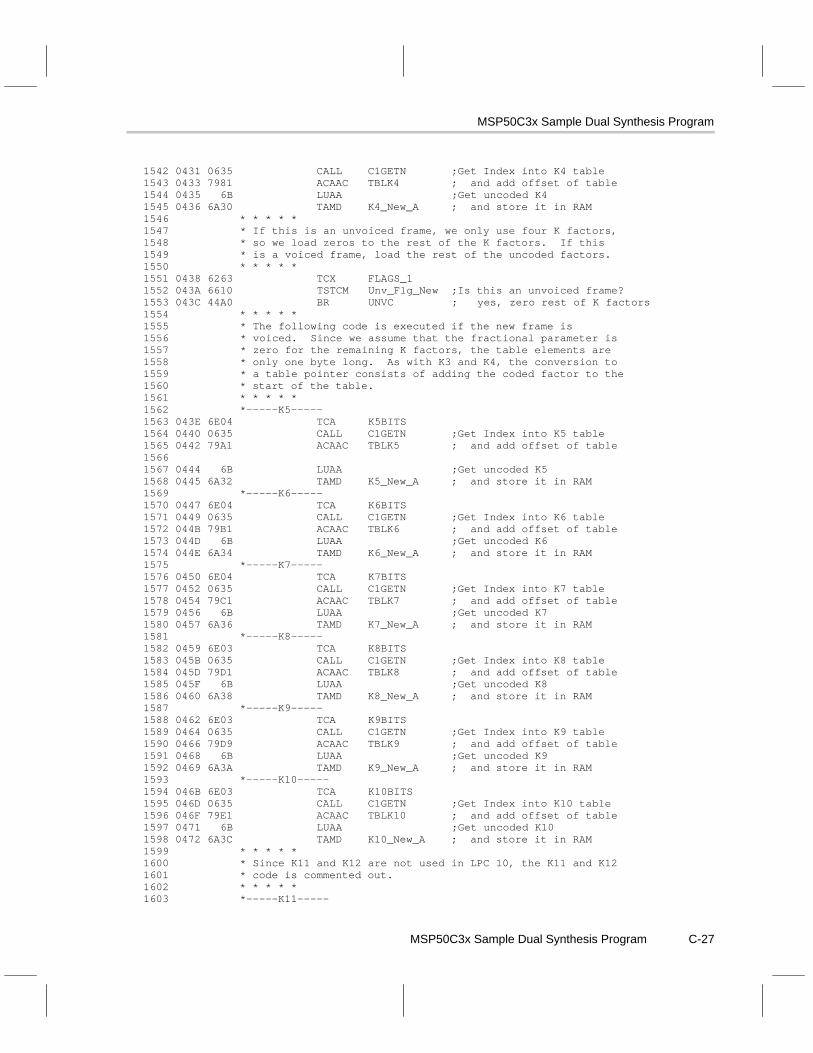
MSP50C3x Sample Dual Synthesis Program
C-27 MSP50C3x Sample Dual Synthesis Program
1542 0431 0635 CALL C1GETN ;Get Index into K4 table1543 0433 7981 ACAAC TBLK4 ; and add offset of table1544 0435 6B LUAA ;Get uncoded K41545 0436 6A30 TAMD K4_New_A ; and store it in RAM1546 * * * * *1547 * If this is an unvoiced frame, we only use four K factors,1548 * so we load zeros to the rest of the K factors. If this1549 * is a voiced frame, load the rest of the uncoded factors.1550 * * * * *1551 0438 6263 TCX FLAGS_11552 043A 6610 TSTCM Unv_Flg_New ;Is this an unvoiced frame?1553 043C 44A0 BR UNVC ; yes, zero rest of K factors1554 * * * * *1555 * The following code is executed if the new frame is1556 * voiced. Since we assume that the fractional parameter is1557 * zero for the remaining K factors, the table elements are1558 * only one byte long. As with K3 and K4, the conversion to1559 * a table pointer consists of adding the coded factor to the1560 * start of the table.1561 * * * * *1562 *–––––K5–––––1563 043E 6E04 TCA K5BITS1564 0440 0635 CALL C1GETN ;Get Index into K5 table1565 0442 79A1 ACAAC TBLK5 ; and add offset of table15661567 0444 6B LUAA ;Get uncoded K51568 0445 6A32 TAMD K5_New_A ; and store it in RAM1569 *–––––K6–––––1570 0447 6E04 TCA K6BITS1571 0449 0635 CALL C1GETN ;Get Index into K6 table1572 044B 79B1 ACAAC TBLK6 ; and add offset of table1573 044D 6B LUAA ;Get uncoded K61574 044E 6A34 TAMD K6_New_A ; and store it in RAM1575 *–––––K7–––––1576 0450 6E04 TCA K7BITS1577 0452 0635 CALL C1GETN ;Get Index into K7 table1578 0454 79C1 ACAAC TBLK7 ; and add offset of table1579 0456 6B LUAA ;Get uncoded K71580 0457 6A36 TAMD K7_New_A ; and store it in RAM1581 *–––––K8–––––1582 0459 6E03 TCA K8BITS1583 045B 0635 CALL C1GETN ;Get Index into K8 table1584 045D 79D1 ACAAC TBLK8 ; and add offset of table1585 045F 6B LUAA ;Get uncoded K81586 0460 6A38 TAMD K8_New_A ; and store it in RAM1587 *–––––K9–––––1588 0462 6E03 TCA K9BITS1589 0464 0635 CALL C1GETN ;Get Index into K9 table1590 0466 79D9 ACAAC TBLK9 ; and add offset of table1591 0468 6B LUAA ;Get uncoded K91592 0469 6A3A TAMD K9_New_A ; and store it in RAM1593 *–––––K10–––––1594 046B 6E03 TCA K10BITS1595 046D 0635 CALL C1GETN ;Get Index into K10 table1596 046F 79E1 ACAAC TBLK10 ; and add offset of table1597 0471 6B LUAA ;Get uncoded K101598 0472 6A3C TAMD K10_New_A ; and store it in RAM1599 * * * * *1600 * Since K11 and K12 are not used in LPC 10, the K11 and K121601 * code is commented out.1602 * * * * *1603 *–––––K11–––––
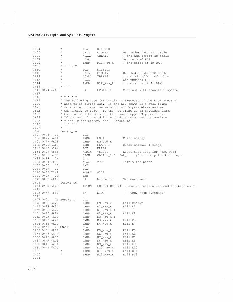
MSP50C3x Sample Dual Synthesis Program
C-28
1604 * TCA K11BITS1605 * CALL C1GETN ;Get Index into K11 table1606 * ACAAC TBLK11 ; and add offset of table1607 * LUAA ;Get uncoded K111608 * TAMD K11_New_A ; and store it in RAM1609 *–––––K12–––––1610 * TCA K11BITS1611 * CALL C1GETN ;Get Index into K12 table1612 * ACAAC TBLK12 ; and add offset of table1613 * LUAA ;Get uncoded K121614 * TAMD K12_New_A ; and store it in RAM1615 *–––––1616 0474 44AD BR UPDATE_2 ;Continue with channel 2 update16171618 * * * * *1619 * The following code (ZeroKs_1) is executed if the K parameters1620 * need to be zeroed out. If the new frame is a stop frame1621 * or a silent frame, we zero out all K parameters and set1622 * the energy to zero. If the new frame is an unvoiced frame,1623 * then we need to zero out the unused upper K parameters.1624 * If the end of a word is reached, then we set appropriate1625 * flags, clear energy, etc. (ZeroKs_1a)1626 * * * * *1627 *1628 ZeroKs_1a1629 0476 2F CLA1630 0477 6A01 TAMD EN_A ;Clear energy1631 0479 6A21 TAMD EN_Old_A1632 047B 6A63 TAMD FLAGS_1 ;Clear channel 1 flags1633 047D 6262 TCX FLAGS1634 047F 65FE ANDCM ~Stop1 ;Reset Stop flag for next word1635 0481 6430 ORCM Ch1Inh_1+Ch1Inh_2 ;Set interp inhibit flags1636 0483 2F CLA1637 0484 7FF3 ACAAC #FF3 ;Initialize pitch1638 0486 18 TAX1639 0487 2F CLA1640 0488 7162 ACAAC #1621641 048A 16 TAM1642 048B 406E BR Nxt_Word1 ;Get next word1643 ZeroKs_1b1644 048D 660C TSTCM CH1END+CH2END ;Have we reached the end for both chan-nels1645 048F 45E2 BR STOP ; yes, stop synthesis16461647 0491 2F ZeroKs_1 CLA1648 0492 6A20 TAMD EN_New_A ;Kill Energy1649 0494 6A26 TAMD K1_New_A ;Kill K11650 0496 6A27 TAMD K1_New_A+11651 0498 6A2A TAMD K2_New_A ;Kill K21652 049A 6A2B TAMD K2_New_A+11653 049C 6A2E TAMD K3_New_A ;Kill K31654 049E 6A30 TAMD K4_New_A ;Kill K41655 04A0 2F UNVC CLA1656 04A1 6A32 TAMD K5_New_A ;Kill K51657 04A3 6A34 TAMD K6_New_A ;Kill K61658 04A5 6A36 TAMD K7_New_A ;Kill K71659 04A7 6A38 TAMD K8_New_A ;Kill K81660 04A9 6A3A TAMD K9_New_A ;Kill K91661 04AB 6A3C TAMD K10_New_A ;Kill K101662 * TAMD K11_New_A ;Kill K111663 * TAMD K12_New_A ;Kill K121664
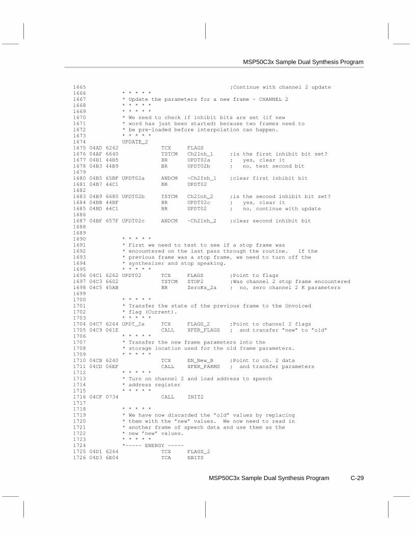
MSP50C3x Sample Dual Synthesis Program
C-29 MSP50C3x Sample Dual Synthesis Program
1665 ;Continue with channel 2 update1666 * * * * *1667 * Update the parameters for a new frame – CHANNEL 21668 * * * * *1669 * * * * *1670 * We need to check if inhibit bits are set (if new1671 * word has just been started) because two frames need to1672 * be pre–loaded before interpolation can happen.1673 * * * * *1674 UPDATE_21675 04AD 6262 TCX FLAGS1676 04AF 6640 TSTCM Ch2Inh_1 ;is the first inhibit bit set?1677 04B1 44B5 BR UPDT02a ; yes, clear it1678 04B3 44B9 BR UPDT02b ; no, test second bit16791680 04B5 65BF UPDT02a ANDCM ~Ch2Inh_1 ;clear first inhibit bit1681 04B7 44C1 BR UPDT0216821683 04B9 6680 UPDT02b TSTCM Ch2Inh_2 ;is the second inhibit bit set?1684 04BB 44BF BR UPDT02c ; yes, clear it1685 04BD 44C1 BR UPDT02 ; no, continue with update16861687 04BF 657F UPDT02c ANDCM ~Ch2Inh_2 ;clear second inhibit bit168816891690 * * * * *1691 * First we need to test to see if a stop frame was1692 * encountered on the last pass through the routine. If the1693 * previous frame was a stop frame, we need to turn off the1694 * synthesizer and stop speaking.1695 * * * * *1696 04C1 6262 UPDT02 TCX FLAGS ;Point to flags1697 04C3 6602 TSTCM STOP2 ;Was channel 2 stop frame encountered1698 04C5 45AB BR ZeroKs_2a ; no, zero channel 2 K parameters16991700 * * * * *1701 * Transfer the state of the previous frame to the Unvoiced1702 * flag (Current).1703 * * * * *1704 04C7 6264 UPDT_2a TCX FLAGS_2 ;Point to channel 2 flags1705 04C9 061E CALL XFER_FLAGS ; and transfer ”new” to ”old”1706 * * * * *1707 * Transfer the new frame parameters into the1708 * storage location used for the old frame parameters.1709 * * * * *1710 04CB 6240 TCX EN_New_B ;Point to ch. 2 data1711 04CD 06EF CALL XFER_PARMS ; and transfer parameters1712 * * * * *1713 * Turn on channel 2 and load address to speech1714 * address register1715 * * * * *1716 04CF 0734 CALL INIT217171718 * * * * *1719 * We have now discarded the ”old” values by replacing1720 * them with the ”new” values. We now need to read in1721 * another frame of speech data and use them as the1722 * new ”new” values.1723 * * * * *1724 *––––– ENERGY –––––1725 04D1 6264 TCX FLAGS_21726 04D3 6E04 TCA EBITS
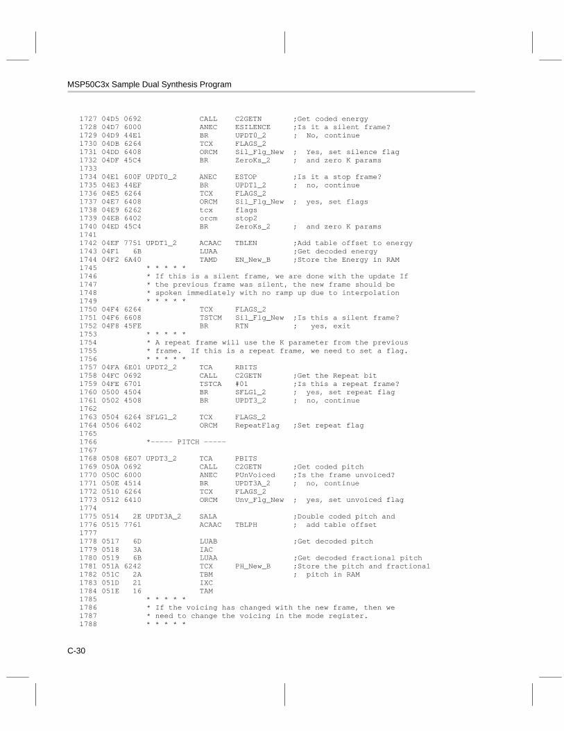
MSP50C3x Sample Dual Synthesis Program
C-30
1727 04D5 0692 CALL C2GETN ;Get coded energy1728 04D7 6000 ANEC ESILENCE ;Is it a silent frame?1729 04D9 44E1 BR UPDT0_2 ; No, continue1730 04DB 6264 TCX FLAGS_21731 04DD 6408 ORCM Sil_Flg_New ; Yes, set silence flag1732 04DF 45C4 BR ZeroKs_2 ; and zero K params17331734 04E1 600F UPDT0_2 ANEC ESTOP ;Is it a stop frame?1735 04E3 44EF BR UPDT1_2 ; no, continue1736 04E5 6264 TCX FLAGS_21737 04E7 6408 ORCM Sil_Flg_New ; yes, set flags1738 04E9 6262 tcx flags1739 04EB 6402 orcm stop21740 04ED 45C4 BR ZeroKs_2 ; and zero K params17411742 04EF 7751 UPDT1_2 ACAAC TBLEN ;Add table offset to energy1743 04F1 6B LUAA ;Get decoded energy1744 04F2 6A40 TAMD EN_New_B ;Store the Energy in RAM1745 * * * * *1746 * If this is a silent frame, we are done with the update If1747 * the previous frame was silent, the new frame should be1748 * spoken immediately with no ramp up due to interpolation1749 * * * * *1750 04F4 6264 TCX FLAGS_21751 04F6 6608 TSTCM Sil_Flg_New ;Is this a silent frame?1752 04F8 45FE BR RTN ; yes, exit1753 * * * * *1754 * A repeat frame will use the K parameter from the previous1755 * frame. If this is a repeat frame, we need to set a flag.1756 * * * * *1757 04FA 6E01 UPDT2_2 TCA RBITS1758 04FC 0692 CALL C2GETN ;Get the Repeat bit1759 04FE 6701 TSTCA #01 ;Is this a repeat frame?1760 0500 4504 BR SFLG1_2 ; yes, set repeat flag1761 0502 4508 BR UPDT3_2 ; no, continue17621763 0504 6264 SFLG1_2 TCX FLAGS_21764 0506 6402 ORCM RepeatFlag ;Set repeat flag17651766 *––––– PITCH –––––17671768 0508 6E07 UPDT3_2 TCA PBITS1769 050A 0692 CALL C2GETN ;Get coded pitch1770 050C 6000 ANEC PUnVoiced ;Is the frame unvoiced?1771 050E 4514 BR UPDT3A_2 ; no, continue1772 0510 6264 TCX FLAGS_21773 0512 6410 ORCM Unv_Flg_New ; yes, set unvoiced flag17741775 0514 2E UPDT3A_2 SALA ;Double coded pitch and1776 0515 7761 ACAAC TBLPH ; add table offset17771778 0517 6D LUAB ;Get decoded pitch1779 0518 3A IAC1780 0519 6B LUAA ;Get decoded fractional pitch1781 051A 6242 TCX PH_New_B ;Store the pitch and fractional1782 051C 2A TBM ; pitch in RAM1783 051D 21 IXC1784 051E 16 TAM1785 * * * * *1786 * If the voicing has changed with the new frame, then we1787 * need to change the voicing in the mode register.1788 * * * * *
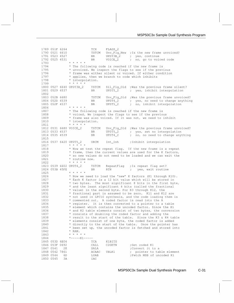
MSP50C3x Sample Dual Synthesis Program
C-31 MSP50C3x Sample Dual Synthesis Program
1789 051F 6264 TCX FLAGS_21790 0521 6610 TSTCM Unv_Flg_New ;Is the new frame unvoiced?1791 0523 4527 BR UPDT3B_2 ; yes, continue1792 0525 4531 BR VOICE_2 ; no, go to voiced code1793 * * * * *1794 * The following code is reached if the new frame is1795 * unvoiced. We inspect the flags to see if the previous1796 * frame was either silent or voiced. If either condition1797 * applies, then we branch to code which inhibits1798 * interpolation.1799 * * * * *1800 0527 6640 UPDT3B_2 TSTCM Sil_Flg_Old ;Was the previous frame silent?1801 0529 4537 BR UPDT5_2 ; yes, inhibit interpolation18021803 052B 6680 TSTCM Unv_Flg_Old ;Was the previous frame unvoiced?1804 052D 4539 BR UPDT4_2 ; yes, no need to change anything1805 052F 4537 BR UPDT5_2 ; no, inhibit interpolation1806 * * * * *1807 * The following code is reached if the new frame is1808 * voiced. We inspect the flags to see if the previous1809 * frame was also voiced. If it was not, we need to inhibit1810 * interpolation.1811 * * * * *1812 0531 6680 VOICE_2 TSTCM Unv_Flg_Old ;Was the previous frame unvoiced?1813 0533 4537 BR UPDT5_2 ; yes, set no interpolation1814 0535 4539 BR UPDT4_2 ; no, no need to change anything18151816 0537 6420 UPDT5_2 ORCM Int_Inh ;Inhibit interpolation1817 * * * * *1818 * Now we test the repeat flag. If the new frame is a repeat1819 * frame, then the current values are used for the K factors,1820 * so new values do not need to be loaded and we can exit the1821 * routine now.1822 * * * * *1823 0539 6602 UPDT4_2 TSTCM RepeatFlag ;Is repeat flag set?1824 053B 45FE BR RTN ; yes, exit routine1825 * * * * *1826 * Now we need to load the ”new” K factors (K1 through K10).1827 * Each K factor is a 12 bit value which will be stored in1828 * two bytes. The most significant 8 bits in the first byte,1829 * and the least significant 4 bits (called the fractional1830 * value) in the second byte. For K3 through K12, the1831 * fractional part is assumed to be zero. K11 and K12 are1832 * not used in LPC10 synthesis, and the code loading them is1833 * commented out. A coded factor is read into the A1834 * register. It is then converted to a pointer to a table1835 * element which contains the uncoded factor. Since the K11836 * and K2 table elements consist of two bytes, the conversion1837 * consists of doubling the coded factor and adding the1838 * result to the start of the table. Since the K3 & K4 table1839 * elements consist of one byte, the coded factor is added1840 * directly to the start of the table. Once the pointer has1841 * been set up, the uncoded factor is fetched and stored into1842 * RAM.1843 * * * * *1844 *–––––K1–––––1845 053D 6E06 TCA K1BITS1846 053F 0692 CALL C2GETN ;Get coded K11847 0541 2E SALA ;Convert it to a1848 0542 7861 ACAAC TBLK1 ; pointer to table element1849 0544 6D LUAB ;Fetch MSB of uncoded K11850 0545 3A IAC
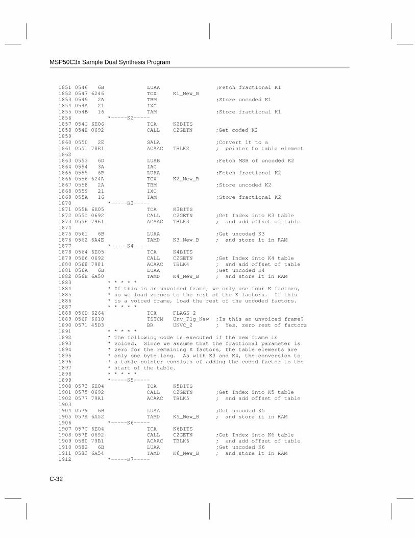
MSP50C3x Sample Dual Synthesis Program
C-32
1851 0546 6B LUAA ;Fetch fractional K11852 0547 6246 TCX K1_New_B1853 0549 2A TBM ;Store uncoded K11854 054A 21 IXC1855 054B 16 TAM ;Store fractional K11856 *–––––K2–––––1857 054C 6E06 TCA K2BITS1858 054E 0692 CALL C2GETN ;Get coded K218591860 0550 2E SALA ;Convert it to a1861 0551 78E1 ACAAC TBLK2 ; pointer to table element18621863 0553 6D LUAB ;Fetch MSB of uncoded K21864 0554 3A IAC1865 0555 6B LUAA ;Fetch fractional K21866 0556 624A TCX K2_New_B1867 0558 2A TBM ;Store uncoded K21868 0559 21 IXC1869 055A 16 TAM ;Store fractional K21870 *–––––K3–––––1871 055B 6E05 TCA K3BITS1872 055D 0692 CALL C2GETN ;Get Index into K3 table1873 055F 7961 ACAAC TBLK3 ; and add offset of table18741875 0561 6B LUAA ;Get uncoded K31876 0562 6A4E TAMD K3_New_B ; and store it in RAM1877 *–––––K4–––––1878 0564 6E05 TCA K4BITS1879 0566 0692 CALL C2GETN ;Get Index into K4 table1880 0568 7981 ACAAC TBLK4 ; and add offset of table1881 056A 6B LUAA ;Get uncoded K41882 056B 6A50 TAMD K4_New_B ; and store it in RAM1883 * * * * *1884 * If this is an unvoiced frame, we only use four K factors,1885 * so we load zeroes to the rest of the K factors. If this1886 * is a voiced frame, load the rest of the uncoded factors.1887 * * * * *1888 056D 6264 TCX FLAGS_21889 056F 6610 TSTCM Unv_Flg_New ;Is this an unvoiced frame?1890 0571 45D3 BR UNVC_2 ; Yes, zero rest of factors1891 * * * * *1892 * The following code is executed if the new frame is1893 * voiced. Since we assume that the fractional parameter is1894 * zero for the remaining K factors, the table elements are1895 * only one byte long. As with K3 and K4, the conversion to1896 * a table pointer consists of adding the coded factor to the1897 * start of the table.1898 * * * * *1899 *–––––K5–––––1900 0573 6E04 TCA K5BITS1901 0575 0692 CALL C2GETN ;Get Index into K5 table1902 0577 79A1 ACAAC TBLK5 ; and add offset of table19031904 0579 6B LUAA ;Get uncoded K51905 057A 6A52 TAMD K5_New_B ; and store it in RAM1906 *–––––K6–––––1907 057C 6E04 TCA K6BITS1908 057E 0692 CALL C2GETN ;Get Index into K6 table1909 0580 79B1 ACAAC TBLK6 ; and add offset of table1910 0582 6B LUAA ;Get uncoded K61911 0583 6A54 TAMD K6_New_B ; and store it in RAM1912 *–––––K7–––––
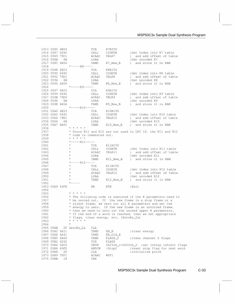
MSP50C3x Sample Dual Synthesis Program
C-33 MSP50C3x Sample Dual Synthesis Program
1913 0585 6E04 TCA K7BITS1914 0587 0692 CALL C2GETN ;Get Index into K7 table1915 0589 79C1 ACAAC TBLK7 ; and add offset of table1916 058B 6B LUAA ;Get uncoded K71917 058C 6A56 TAMD K7_New_B ; and store it in RAM1918 *–––––K8–––––1919 058E 6E03 TCA K8BITS1920 0590 0692 CALL C2GETN ;Get Index into K8 table1921 0592 79D1 ACAAC TBLK8 ; and add offset of table1922 0594 6B LUAA ;Get uncoded K81923 0595 6A58 TAMD K8_New_B ; and store it in RAM1924 *–––––K9–––––1925 0597 6E03 TCA K9BITS1926 0599 0692 CALL C2GETN ;Get Index into K9 table1927 059B 79D9 ACAAC TBLK9 ; and add offset of table1928 059D 6B LUAA ;Get uncoded K91929 059E 6A5A TAMD K9_New_B ; and store it in RAM1930 *–––––K10–––––1931 05A0 6E03 TCA K10BITS1932 05A2 0692 CALL C2GETN ;Get Index into K10 table1933 05A4 79E1 ACAAC TBLK10 ; and add offset of table1934 05A6 6B LUAA ;Get uncoded K101935 05A7 6A5C TAMD K10_New_B ; and store it in RAM1936 * * * * *1937 * Since K11 and K12 are not used in LPC 10, the K11 and K121938 * code is commented out.1939 * * * * *1940 *–––––K11–––––1941 * TCA K11BITS1942 * CALL C2GETN ;Get Index into K11 table1943 * ACAAC TBLK11 ; and add offset of table1944 * LUAA ;Get uncoded K111945 * TAMD K11_New_B ; and store it in RAM1946 *–––––K12–––––1947 * TCA K11BITS1948 * CALL C2GETN ;Get Index into K12 table1949 * ACAAC TBLK12 ; and add offset of table1950 * LUAA ;Get uncoded K121951 * TAMD K12_New_B ; and store it in RAM1952 *–––––1953 05A9 45FE BR RTN ;Exit19541955 * * * * *1956 * The following code is executed if the K parameters need to1957 * be zeroed out. If the new frame is a stop frame or a1958 * silent frame, we zero out all K parameters and set the1959 * energy to zero. If the new frame is an unvoiced frame,1960 * then we need to zero out the unused upper K parameters.1961 * If the end of a word is reached, then we set appropriate1962 * flags, clear energy, etc. (ZeroKs_2a)1963 * * * * *1964 *1965 05AB 2F ZeroKs_2a CLA1966 05AC 6A11 TAMD EN_B ;clear energy1967 05AE 6A41 TAMD EN_Old_B1968 05B0 6A64 TAMD FLAGS_2 ;clear channel 2 flags1969 05B2 6262 TCX FLAGS1970 05B4 64C0 ORCM Ch2Inh_1+Ch2Inh_2 ;set interp inhibit flags1971 05B6 65FD ANDCM ~Stop2 ;reset stop flag for next word1972 05B8 2F CLA ;initialize pitch1973 05B9 7FF1 ACAAC #FF11974 05BB 18 TAX
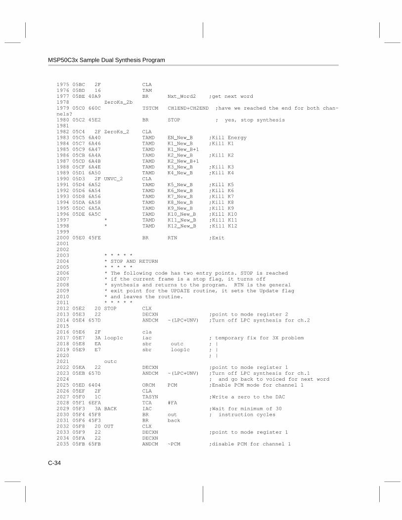
MSP50C3x Sample Dual Synthesis Program
C-34
1975 05BC 2F CLA1976 05BD 16 TAM1977 05BE 40A9 BR Nxt_Word2 ;get next word1978 ZeroKs_2b1979 05C0 660C TSTCM CH1END+CH2END ;have we reached the end for both chan-nels?1980 05C2 45E2 BR STOP ; yes, stop synthesis19811982 05C4 2F ZeroKs_2 CLA1983 05C5 6A40 TAMD EN_New_B ;Kill Energy1984 05C7 6A46 TAMD K1_New_B ;Kill K11985 05C9 6A47 TAMD K1_New_B+11986 05CB 6A4A TAMD K2_New_B ;Kill K21987 05CD 6A4B TAMD K2_New_B+11988 05CF 6A4E TAMD K3_New_B ;Kill K31989 05D1 6A50 TAMD K4_New_B ;Kill K41990 05D3 2F UNVC_2 CLA1991 05D4 6A52 TAMD K5_New_B ;Kill K51992 05D6 6A54 TAMD K6_New_B ;Kill K61993 05D8 6A56 TAMD K7_New_B ;Kill K71994 05DA 6A58 TAMD K8_New_B ;Kill K81995 05DC 6A5A TAMD K9_New_B ;Kill K91996 05DE 6A5C TAMD K10_New_B ;Kill K101997 * TAMD K11_New_B ;Kill K111998 * TAMD K12_New_B ;Kill K1219992000 05E0 45FE BR RTN ;Exit200120022003 * * * * *2004 * STOP AND RETURN2005 * * * * *2006 * The following code has two entry points. STOP is reached2007 * if the current frame is a stop flag, it turns off2008 * synthesis and returns to the program. RTN is the general2009 * exit point for the UPDATE routine, it sets the Update flag2010 * and leaves the routine.2011 * * * * *2012 05E2 20 STOP CLX2013 05E3 22 DECXN ;point to mode register 22014 05E4 657D ANDCM ~(LPC+UNV) ;Turn off LPC synthesis for ch.220152016 05E6 2F cla2017 05E7 3A loop1c iac ; temporary fix for 3X problem2018 05E8 EA sbr outc ; |2019 05E9 E7 sbr loop1c ; |2020 ; |2021 outc2022 05EA 22 DECXN ;point to mode register 12023 05EB 657D ANDCM ~(LPC+UNV) ;Turn off LPC synthesis for ch.12024 ; and go back to voiced for next word2025 05ED 6404 ORCM PCM ;Enable PCM mode for channel 12026 05EF 2F CLA2027 05F0 1C TASYN ;Write a zero to the DAC2028 05F1 6EFA TCA #FA2029 05F3 3A BACK IAC ;Wait for minimum of 302030 05F4 45F8 BR out ; instruction cycles2031 05F6 45F3 BR back2032 05F8 20 OUT CLX2033 05F9 22 DECXN ;point to mode register 12034 05FA 22 DECXN2035 05FB 65FB ANDCM ~PCM ;disable PCM for channel 1
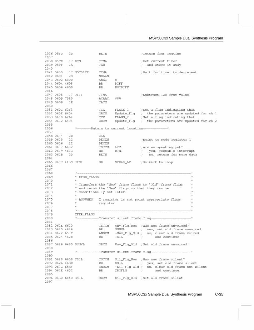
MSP50C3x Sample Dual Synthesis Program
C-35 MSP50C3x Sample Dual Synthesis Program
2036 05FD 3D RETN ;return from routine20372038 05FE 17 RTN TTMA ;Get current timer2039 05FF 1A TAB ; and store it away20402041 0600 17 NOTDIFF TTMA ;Wait for timer to decrement2042 0601 2D SBAAN2043 0602 6000 ANEC 02044 0604 4608 BR DIFF2045 0606 4600 BR NOTDIFF20462047 0608 17 DIFF TTMA ;Subtract 128 from value2048 0609 7080 ACAAC #802049 060B 1E TATM20502051 060C 6263 TCX FLAGS_1 ;Set a flag indicating that2052 060E 6404 ORCM Update_Flg ; the parameters are updated for ch.12053 0610 6264 TCX FLAGS_2 ;Set a flag indicating that2054 0612 6404 ORCM Update_Flg ; the parameters are updated for ch.220552056 *–––––––Return to current location––––––––––––*20572058 0614 20 CLX2059 0615 22 DECXN ;point to mode register 12060 0616 22 DECXN2061 0617 6602 TSTCM LPC ;Are we speaking yet?2062 0619 461C BR RTN1 ; yes, reenable interrupt2063 061B 3D RETN ; no, return for more data20642065 061C 4139 RTN1 BR SPEAK_LP ;Go back to loop206620672068 *–––––––––––––––––––––––––––––––––––––––––––––––––––––––––*2069 * XFER_FLAGS *2070 * *2071 * Transfers the ”New” frame flags to ”Old” frame flags *2072 * and zeros the ”New” flags so that they can be *2073 * conditionally set later. *2074 * *2075 * ASSUMES: X register is set point appropriate flags *2076 * register *2077 * *2078 *–––––––––––––––––––––––––––––––––––––––––––––––––––––––––*2079 XFER_FLAGS2080 *–––––––––––Transfer silent frame flag––––––––––––––––––––*20812082 061E 6610 TSTCM Unv_Flg_New ;Was new frame unvoiced?2083 0620 4626 BR SUNVL ; yes, set old frame unvoiced2084 0622 657F ANDCM ~Unv_Flg_Old ; no, clear old frame voiced2085 0624 4628 BR TSIL ; and continue20862087 0626 6480 SUNVL ORCM Unv_Flg_Old ;Set old frame unvoiced.20882089 *–––––––––––Transfer silent frame flag––––––––––––––––––––*20902091 0628 6608 TSIL TSTCM Sil_Flg_New ;Was new frame silent?2092 062A 4630 BR SSIL ; yes, set old frame silent2093 062C 65BF ANDCM ~Sil_Flg_Old ; no, clear old frame not silent2094 062E 4632 BR ZROFLG ; and continue20952096 0630 6440 SSIL ORCM Sil_Flg_Old ;Set old frame silent2097
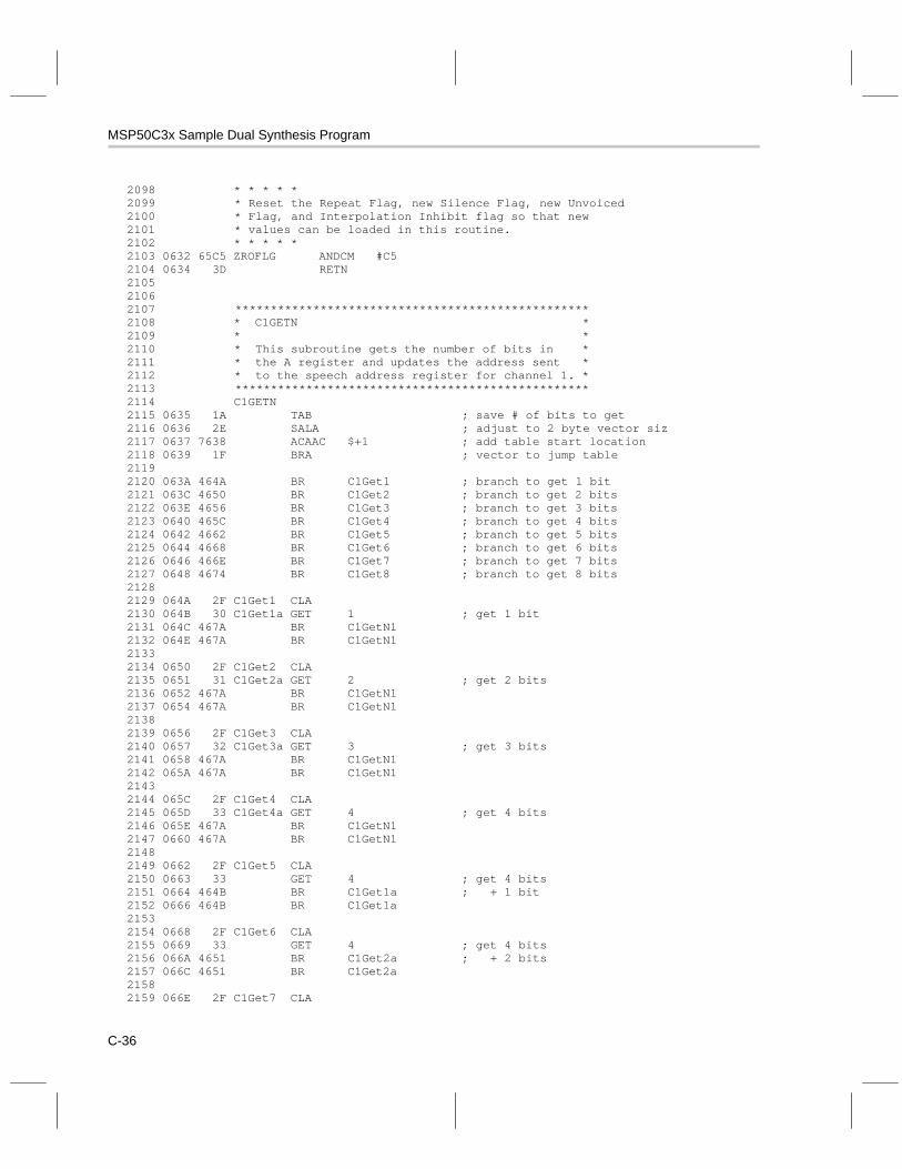
MSP50C3x Sample Dual Synthesis Program
C-36
2098 * * * * *2099 * Reset the Repeat Flag, new Silence Flag, new Unvoiced2100 * Flag, and Interpolation Inhibit flag so that new2101 * values can be loaded in this routine.2102 * * * * *2103 0632 65C5 ZROFLG ANDCM #C52104 0634 3D RETN210521062107 **************************************************2108 * C1GETN *2109 * *2110 * This subroutine gets the number of bits in *2111 * the A register and updates the address sent *2112 * to the speech address register for channel 1. *2113 **************************************************2114 C1GETN2115 0635 1A TAB ; save # of bits to get2116 0636 2E SALA ; adjust to 2 byte vector siz2117 0637 7638 ACAAC $+1 ; add table start location2118 0639 1F BRA ; vector to jump table21192120 063A 464A BR C1Get1 ; branch to get 1 bit2121 063C 4650 BR C1Get2 ; branch to get 2 bits2122 063E 4656 BR C1Get3 ; branch to get 3 bits2123 0640 465C BR C1Get4 ; branch to get 4 bits2124 0642 4662 BR C1Get5 ; branch to get 5 bits2125 0644 4668 BR C1Get6 ; branch to get 6 bits2126 0646 466E BR C1Get7 ; branch to get 7 bits2127 0648 4674 BR C1Get8 ; branch to get 8 bits21282129 064A 2F C1Get1 CLA2130 064B 30 C1Get1a GET 1 ; get 1 bit2131 064C 467A BR C1GetN12132 064E 467A BR C1GetN121332134 0650 2F C1Get2 CLA2135 0651 31 C1Get2a GET 2 ; get 2 bits2136 0652 467A BR C1GetN12137 0654 467A BR C1GetN121382139 0656 2F C1Get3 CLA2140 0657 32 C1Get3a GET 3 ; get 3 bits2141 0658 467A BR C1GetN12142 065A 467A BR C1GetN121432144 065C 2F C1Get4 CLA2145 065D 33 C1Get4a GET 4 ; get 4 bits2146 065E 467A BR C1GetN12147 0660 467A BR C1GetN121482149 0662 2F C1Get5 CLA2150 0663 33 GET 4 ; get 4 bits2151 0664 464B BR C1Get1a ; + 1 bit2152 0666 464B BR C1Get1a21532154 0668 2F C1Get6 CLA2155 0669 33 GET 4 ; get 4 bits2156 066A 4651 BR C1Get2a ; + 2 bits2157 066C 4651 BR C1Get2a21582159 066E 2F C1Get7 CLA
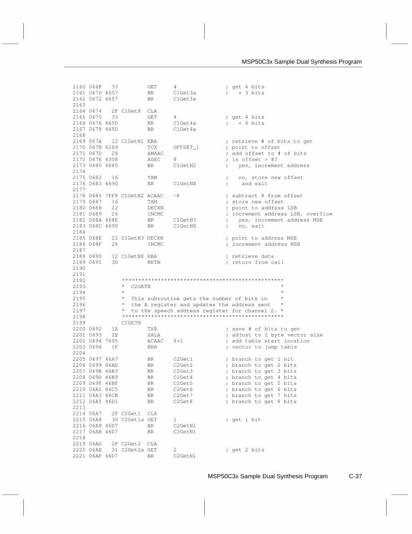
MSP50C3x Sample Dual Synthesis Program
C-37 MSP50C3x Sample Dual Synthesis Program
2160 066F 33 GET 4 ; get 4 bits2161 0670 4657 BR C1Get3a ; + 3 bits2162 0672 4657 BR C1Get3a21632164 0674 2F C1Get8 CLA2165 0675 33 GET 4 ; get 4 bits2166 0676 465D BR C1Get4a ; + 4 bits2167 0678 465D BR C1Get4a21682169 067A 12 C1GetN1 XBA ; retrieve # of bits to get2170 067B 6269 TCX OFFSET_1 ; point to offset2171 067D 28 AMAAC ; add offset to # of bits2172 067E 6308 AGEC 8 ; is offset > 8?2173 0680 4685 BR C1GetN2 ; yes, increment address21742175 0682 16 TAM ; no, store new offset2176 0683 4690 BR C1GetNX ; and exit21772178 0685 7FF8 C1GetN2 ACAAC –8 ; subtract 8 from offset2179 0687 16 TAM ; store new offset2180 0688 22 DECXN ; point to address LSB2181 0689 26 INCMC ; increment address LSB, overflow2182 068A 468E BR C1GetN3 ; yes, increment address MSB2183 068C 4690 BR C1GetNX ; no, exit21842185 068E 22 C1GetN3 DECXN ; point to address MSB2186 068F 26 INCMC ; increment address MSB21872188 0690 12 C1GetNX XBA ; retrieve data2189 0691 3D RETN ; return from call219021912192 **************************************************2193 * C2GETN *2194 * *2195 * This subroutine gets the number of bits in *2196 * the A register and updates the address sent *2197 * to the speech address register for channel 2. *2198 **************************************************2199 C2GETN2200 0692 1A TAB ; save # of bits to get2201 0693 2E SALA ; adjust to 2 byte vector size2202 0694 7695 ACAAC $+1 ; add table start location2203 0696 1F BRA ; vector to jump table22042205 0697 46A7 BR C2Get1 ; branch to get 1 bit2206 0699 46AD BR C2Get2 ; branch to get 2 bits2207 069B 46B3 BR C2Get3 ; branch to get 3 bits2208 069D 46B9 BR C2Get4 ; branch to get 4 bits2209 069F 46BF BR C2Get5 ; branch to get 5 bits2210 06A1 46C5 BR C2Get6 ; branch to get 6 bits2211 06A3 46CB BR C2Get7 ; branch to get 7 bits2212 06A5 46D1 BR C2Get8 ; branch to get 8 bits22132214 06A7 2F C2Get1 CLA2215 06A8 30 C2Get1a GET 1 ; get 1 bit2216 06A9 46D7 BR C2GetN12217 06AB 46D7 BR C2GetN122182219 06AD 2F C2Get2 CLA2220 06AE 31 C2Get2a GET 2 ; get 2 bits2221 06AF 46D7 BR C2GetN1
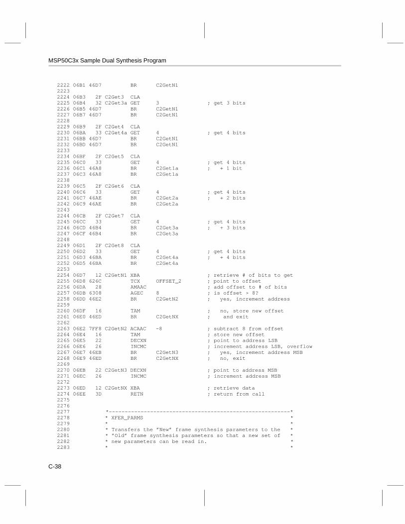
MSP50C3x Sample Dual Synthesis Program
C-38
2222 06B1 46D7 BR C2GetN122232224 06B3 2F C2Get3 CLA2225 06B4 32 C2Get3a GET 3 ; get 3 bits2226 06B5 46D7 BR C2GetN12227 06B7 46D7 BR C2GetN122282229 06B9 2F C2Get4 CLA2230 06BA 33 C2Get4a GET 4 ; get 4 bits2231 06BB 46D7 BR C2GetN12232 06BD 46D7 BR C2GetN122332234 06BF 2F C2Get5 CLA2235 06C0 33 GET 4 ; get 4 bits2236 06C1 46A8 BR C2Get1a ; + 1 bit2237 06C3 46A8 BR C2Get1a22382239 06C5 2F C2Get6 CLA2240 06C6 33 GET 4 ; get 4 bits2241 06C7 46AE BR C2Get2a ; + 2 bits2242 06C9 46AE BR C2Get2a22432244 06CB 2F C2Get7 CLA2245 06CC 33 GET 4 ; get 4 bits2246 06CD 46B4 BR C2Get3a ; + 3 bits2247 06CF 46B4 BR C2Get3a22482249 06D1 2F C2Get8 CLA2250 06D2 33 GET 4 ; get 4 bits2251 06D3 46BA BR C2Get4a ; + 4 bits2252 06D5 46BA BR C2Get4a22532254 06D7 12 C2GetN1 XBA ; retrieve # of bits to get2255 06D8 626C TCX OFFSET_2 ; point to offset2256 06DA 28 AMAAC ; add offset to # of bits2257 06DB 6308 AGEC 8 ; is offset > 8?2258 06DD 46E2 BR C2GetN2 ; yes, increment address22592260 06DF 16 TAM ; no, store new offset2261 06E0 46ED BR C2GetNX ; and exit22622263 06E2 7FF8 C2GetN2 ACAAC –8 ; subtract 8 from offset2264 06E4 16 TAM ; store new offset2265 06E5 22 DECXN ; point to address LSB2266 06E6 26 INCMC ; increment address LSB, overflow2267 06E7 46EB BR C2GetN3 ; yes, increment address MSB2268 06E9 46ED BR C2GetNX ; no, exit22692270 06EB 22 C2GetN3 DECXN ; point to address MSB2271 06EC 26 INCMC ; increment address MSB22722273 06ED 12 C2GetNX XBA ; retrieve data2274 06EE 3D RETN ; return from call227522762277 *–––––––––––––––––––––––––––––––––––––––––––––––––––––––––*2278 * XFER_PARMS *2279 * *2280 * Transfers the ”New” frame synthesis parameters to the *2281 * ”Old” frame synthesis parameters so that a new set of *2282 * new parameters can be read in. *2283 * *
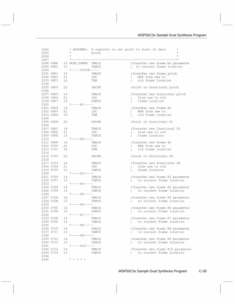
MSP50C3x Sample Dual Synthesis Program
C-39 MSP50C3x Sample Dual Synthesis Program
2284 * ASSUMES: X register is set point to start of data *2285 * block *2286 * *2287 *–––––––––––––––––––––––––––––––––––––––––––––––––––––––––*2288 06EF 14 XFER_PARMS TMAIX ;Transfer new frame En parameter2289 06F0 13 TAMIX ; to current frame location2290 *–––––PITCH–––––2291 06F1 14 TMAIX ;Transfer new frame pitch2292 06F2 21 IXC ; MSB from new to2293 06F3 16 TAM ; old frame location22942295 06F4 22 DECXN ;Point to fractional pitch22962297 06F5 14 TMAIX ;Transfer new fractional pitch2298 06F6 21 IXC ; from new to old2299 06F7 13 TAMIX ; frame location2300 *–––––K1–––––2301 06F8 14 TMAIX ;Transfer new frame K12302 06F9 21 IXC ; MSB from new to2303 06FA 16 TAM ; old frame location23042305 06FB 22 DECXN ;Point to fractional K123062307 06FC 14 TMAIX ;Transfer new fractional K12308 06FD 21 IXC ; from new to old2309 06FE 13 TAMIX ; frame location2310 *–––––K2–––––2311 06FF 14 TMAIX ;Transfer new frame K22312 0700 21 IXC ; MSB from new to2313 0701 16 TAM ; old frame location23142315 0702 22 DECXN ;Point to fractional K223162317 0703 14 TMAIX ;Transfer new fractional K22318 0704 21 IXC ; from new to old2319 0705 13 TAMIX ; frame location2320 *–––––K3–––––2321 0706 14 TMAIX ;Transfer new frame K3 parameter2322 0707 13 TAMIX ; to current frame location2323 *–––––K4–––––2324 0708 14 TMAIX ;Transfer new frame K4 parameter2325 0709 13 TAMIX ; to current frame location2326 *–––––K5–––––2327 070A 14 TMAIX ;Transfer new frame K5 parameter2328 070B 13 TAMIX ; to current frame location2329 *–––––K6–––––2330 070C 14 TMAIX ;Transfer new frame K6 parameter2331 070D 13 TAMIX ; to current frame location2332 *–––––K7–––––2333 070E 14 TMAIX ;Transfer new frame K7 parameter2334 070F 13 TAMIX ; to current frame location2335 *–––––K8–––––2336 0710 14 TMAIX ;Transfer new frame K8 parameter2337 0711 13 TAMIX ; to current frame location2338 *–––––K9–––––2339 0712 14 TMAIX ;Transfer new frame K9 parameter2340 0713 13 TAMIX ; to current frame location2341 *–––––K10–––––2342 0714 14 TMAIX ;Transfer new frame K10 parameter2343 0715 13 TAMIX ; to current frame location23442345 * * * * *
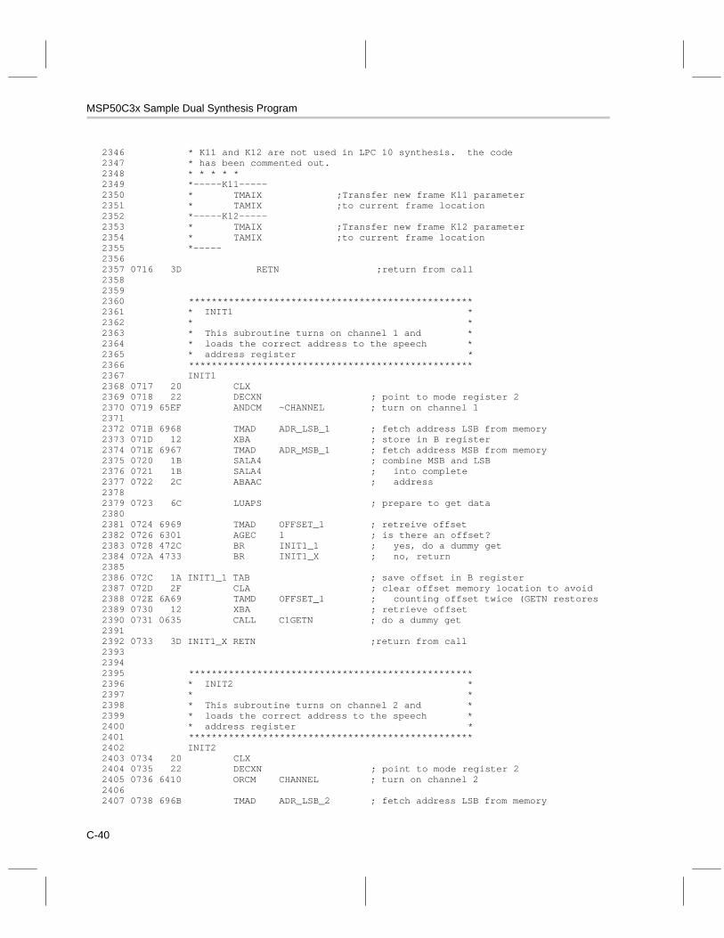
MSP50C3x Sample Dual Synthesis Program
C-40
2346 * K11 and K12 are not used in LPC 10 synthesis. the code2347 * has been commented out.2348 * * * * *2349 *–––––K11–––––2350 * TMAIX ;Transfer new frame K11 parameter2351 * TAMIX ;to current frame location2352 *–––––K12–––––2353 * TMAIX ;Transfer new frame K12 parameter2354 * TAMIX ;to current frame location2355 *–––––23562357 0716 3D RETN ;return from call235823592360 **************************************************2361 * INIT1 *2362 * *2363 * This subroutine turns on channel 1 and *2364 * loads the correct address to the speech *2365 * address register *2366 **************************************************2367 INIT12368 0717 20 CLX2369 0718 22 DECXN ; point to mode register 22370 0719 65EF ANDCM ~CHANNEL ; turn on channel 123712372 071B 6968 TMAD ADR_LSB_1 ; fetch address LSB from memory2373 071D 12 XBA ; store in B register2374 071E 6967 TMAD ADR_MSB_1 ; fetch address MSB from memory2375 0720 1B SALA4 ; combine MSB and LSB2376 0721 1B SALA4 ; into complete2377 0722 2C ABAAC ; address23782379 0723 6C LUAPS ; prepare to get data23802381 0724 6969 TMAD OFFSET_1 ; retreive offset2382 0726 6301 AGEC 1 ; is there an offset?2383 0728 472C BR INIT1_1 ; yes, do a dummy get2384 072A 4733 BR INIT1_X ; no, return23852386 072C 1A INIT1_1 TAB ; save offset in B register2387 072D 2F CLA ; clear offset memory location to avoid2388 072E 6A69 TAMD OFFSET_1 ; counting offset twice (GETN restores2389 0730 12 XBA ; retrieve offset2390 0731 0635 CALL C1GETN ; do a dummy get23912392 0733 3D INIT1_X RETN ;return from call239323942395 **************************************************2396 * INIT2 *2397 * *2398 * This subroutine turns on channel 2 and *2399 * loads the correct address to the speech *2400 * address register *2401 **************************************************2402 INIT22403 0734 20 CLX2404 0735 22 DECXN ; point to mode register 22405 0736 6410 ORCM CHANNEL ; turn on channel 224062407 0738 696B TMAD ADR_LSB_2 ; fetch address LSB from memory
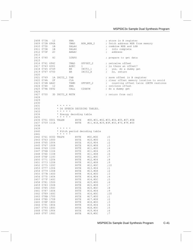
MSP50C3x Sample Dual Synthesis Program
C-41 MSP50C3x Sample Dual Synthesis Program
2408 073A 12 XBA ; store in B register2409 073B 696A TMAD ADR_MSB_2 ; fetch address MSB from memory2410 073D 1B SALA4 ; combine MSB and LSB2411 073E 1B SALA4 ; into complete2412 073F 2C ABAAC ; address24132414 0740 6C LUAPS ; prepare to get data24152416 0741 696C TMAD OFFSET_2 ; retreive offset2417 0743 6301 AGEC 1 ; is there an offset?2418 0745 4749 BR INIT2_1 ; yes, do a dummy get2419 0747 4750 BR INIT2_X ; no, return24202421 0749 1A INIT2_1 TAB ; save offset in B register2422 074A 2F CLA ; clear offset memory location to avoid2423 074B 6A6C TAMD OFFSET_2 ; counting offset twice (GETN restores2424 074D 12 XBA ; retrieve offset2425 074E 0692 CALL C2GETN ; do a dummy get24262427 0750 3D INIT2_X RETN ; return from call2428242924302431 * * * * *2432 * D6 SPEECH DECODING TABLES.2433 * * * * *2434 * Energy decoding table2435 * * * * *2436 0751 0001 TBLEN BYTE #00,#01,#02,#03,#04,#05,#07,#0B2437 0759 111A BYTE #11,#1A,#29,#3F,#55,#70,#7F,#0024382439 * * * * *2440 * Pitch period decoding table2441 * * * * *2442 0761 0C00 TBLPH BYTE #0C,#00 ;02443 0763 1000 BYTE #10,#00 ;12444 0765 1004 BYTE #10,#04 ;22445 0767 1008 BYTE #10,#08 ;32446 0769 1100 BYTE #11,#00 ;42447 076B 1104 BYTE #11,#04 ;52448 076D 1108 BYTE #11,#08 ;62449 076F 110C BYTE #11,#0C ;72450 0771 1204 BYTE #12,#04 ;82451 0773 1208 BYTE #12,#08 ;92452 0775 120C BYTE #12,#0C ;102453 0777 1304 BYTE #13,#04 ;12454 0779 1308 BYTE #13,#08 ;22455 077B 1400 BYTE #14,#00 ;32456 077D 1404 BYTE #14,#04 ;42457 077F 140C BYTE #14,#0C ;52458 0781 1500 BYTE #15,#00 ;62459 0783 1508 BYTE #15,#08 ;72460 0785 150C BYTE #15,#0C ;82461 0787 1604 BYTE #16,#04 ;92462 0789 160C BYTE #16,#0C ;202463 078B 1700 BYTE #17,#00 ;12464 078D 1708 BYTE #17,#08 ;22465 078F 1800 BYTE #18,#00 ;32466 0791 1804 BYTE #18,#04 ;42467 0793 180C BYTE #18,#0C ;52468 0795 1904 BYTE #19,#04 ;62469 0797 190C BYTE #19,#0C ;7
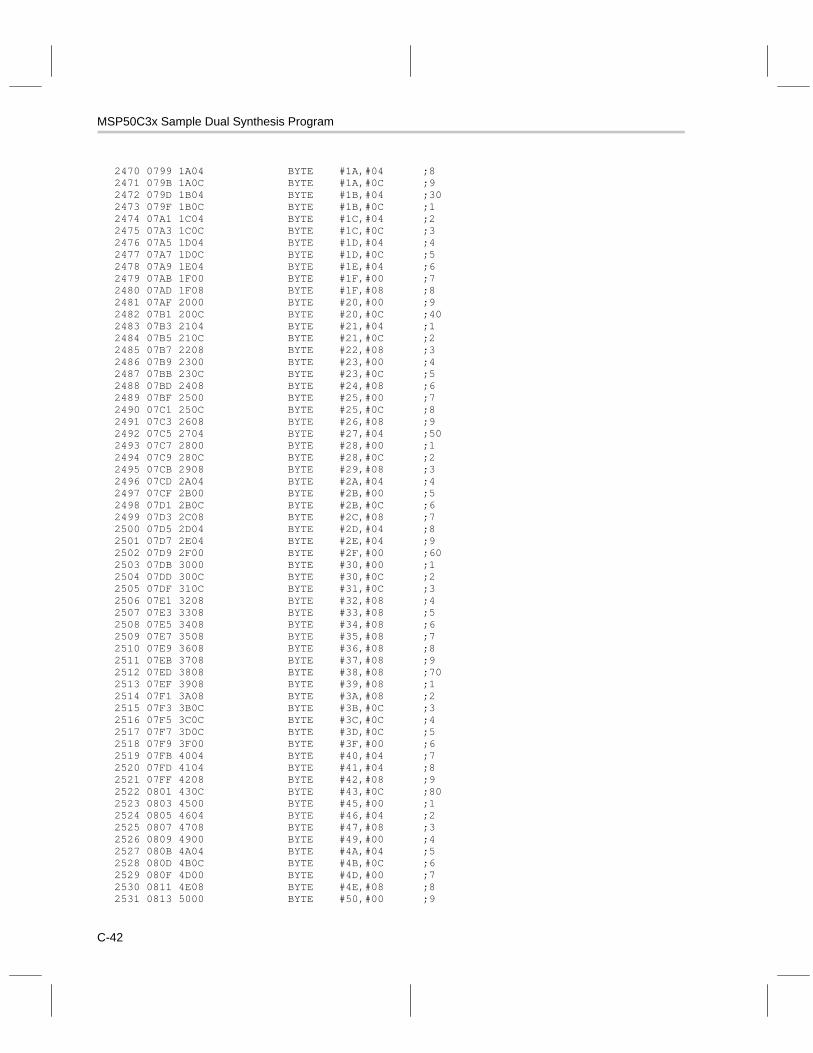
MSP50C3x Sample Dual Synthesis Program
C-42
2470 0799 1A04 BYTE #1A,#04 ;82471 079B 1A0C BYTE #1A,#0C ;92472 079D 1B04 BYTE #1B,#04 ;302473 079F 1B0C BYTE #1B,#0C ;12474 07A1 1C04 BYTE #1C,#04 ;22475 07A3 1C0C BYTE #1C,#0C ;32476 07A5 1D04 BYTE #1D,#04 ;42477 07A7 1D0C BYTE #1D,#0C ;52478 07A9 1E04 BYTE #1E,#04 ;62479 07AB 1F00 BYTE #1F,#00 ;72480 07AD 1F08 BYTE #1F,#08 ;82481 07AF 2000 BYTE #20,#00 ;92482 07B1 200C BYTE #20,#0C ;402483 07B3 2104 BYTE #21,#04 ;12484 07B5 210C BYTE #21,#0C ;22485 07B7 2208 BYTE #22,#08 ;32486 07B9 2300 BYTE #23,#00 ;42487 07BB 230C BYTE #23,#0C ;52488 07BD 2408 BYTE #24,#08 ;62489 07BF 2500 BYTE #25,#00 ;72490 07C1 250C BYTE #25,#0C ;82491 07C3 2608 BYTE #26,#08 ;92492 07C5 2704 BYTE #27,#04 ;502493 07C7 2800 BYTE #28,#00 ;12494 07C9 280C BYTE #28,#0C ;22495 07CB 2908 BYTE #29,#08 ;32496 07CD 2A04 BYTE #2A,#04 ;42497 07CF 2B00 BYTE #2B,#00 ;52498 07D1 2B0C BYTE #2B,#0C ;62499 07D3 2C08 BYTE #2C,#08 ;72500 07D5 2D04 BYTE #2D,#04 ;82501 07D7 2E04 BYTE #2E,#04 ;92502 07D9 2F00 BYTE #2F,#00 ;602503 07DB 3000 BYTE #30,#00 ;12504 07DD 300C BYTE #30,#0C ;22505 07DF 310C BYTE #31,#0C ;32506 07E1 3208 BYTE #32,#08 ;42507 07E3 3308 BYTE #33,#08 ;52508 07E5 3408 BYTE #34,#08 ;62509 07E7 3508 BYTE #35,#08 ;72510 07E9 3608 BYTE #36,#08 ;82511 07EB 3708 BYTE #37,#08 ;92512 07ED 3808 BYTE #38,#08 ;702513 07EF 3908 BYTE #39,#08 ;12514 07F1 3A08 BYTE #3A,#08 ;22515 07F3 3B0C BYTE #3B,#0C ;32516 07F5 3C0C BYTE #3C,#0C ;42517 07F7 3D0C BYTE #3D,#0C ;52518 07F9 3F00 BYTE #3F,#00 ;62519 07FB 4004 BYTE #40,#04 ;72520 07FD 4104 BYTE #41,#04 ;82521 07FF 4208 BYTE #42,#08 ;92522 0801 430C BYTE #43,#0C ;802523 0803 4500 BYTE #45,#00 ;12524 0805 4604 BYTE #46,#04 ;22525 0807 4708 BYTE #47,#08 ;32526 0809 4900 BYTE #49,#00 ;42527 080B 4A04 BYTE #4A,#04 ;52528 080D 4B0C BYTE #4B,#0C ;62529 080F 4D00 BYTE #4D,#00 ;72530 0811 4E08 BYTE #4E,#08 ;82531 0813 5000 BYTE #50,#00 ;9
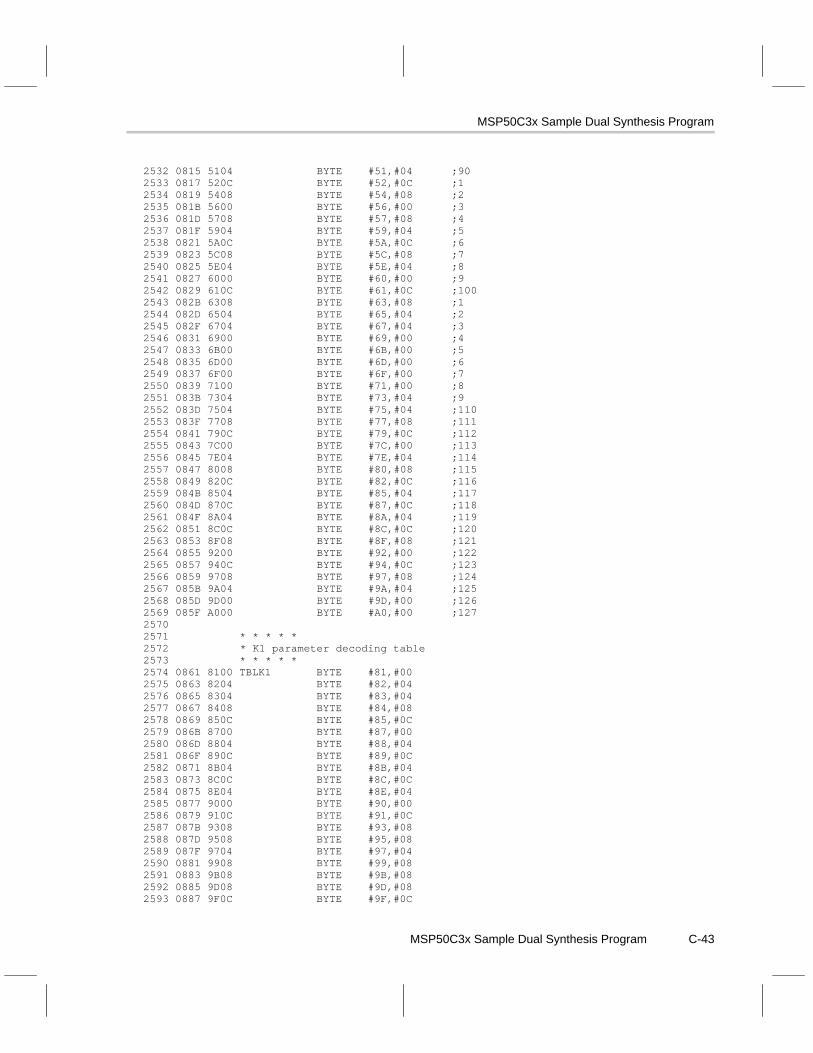
MSP50C3x Sample Dual Synthesis Program
C-43 MSP50C3x Sample Dual Synthesis Program
2532 0815 5104 BYTE #51,#04 ;902533 0817 520C BYTE #52,#0C ;12534 0819 5408 BYTE #54,#08 ;22535 081B 5600 BYTE #56,#00 ;32536 081D 5708 BYTE #57,#08 ;42537 081F 5904 BYTE #59,#04 ;52538 0821 5A0C BYTE #5A,#0C ;62539 0823 5C08 BYTE #5C,#08 ;72540 0825 5E04 BYTE #5E,#04 ;82541 0827 6000 BYTE #60,#00 ;92542 0829 610C BYTE #61,#0C ;1002543 082B 6308 BYTE #63,#08 ;12544 082D 6504 BYTE #65,#04 ;22545 082F 6704 BYTE #67,#04 ;32546 0831 6900 BYTE #69,#00 ;42547 0833 6B00 BYTE #6B,#00 ;52548 0835 6D00 BYTE #6D,#00 ;62549 0837 6F00 BYTE #6F,#00 ;72550 0839 7100 BYTE #71,#00 ;82551 083B 7304 BYTE #73,#04 ;92552 083D 7504 BYTE #75,#04 ;1102553 083F 7708 BYTE #77,#08 ;1112554 0841 790C BYTE #79,#0C ;1122555 0843 7C00 BYTE #7C,#00 ;1132556 0845 7E04 BYTE #7E,#04 ;1142557 0847 8008 BYTE #80,#08 ;1152558 0849 820C BYTE #82,#0C ;1162559 084B 8504 BYTE #85,#04 ;1172560 084D 870C BYTE #87,#0C ;1182561 084F 8A04 BYTE #8A,#04 ;1192562 0851 8C0C BYTE #8C,#0C ;1202563 0853 8F08 BYTE #8F,#08 ;1212564 0855 9200 BYTE #92,#00 ;1222565 0857 940C BYTE #94,#0C ;1232566 0859 9708 BYTE #97,#08 ;1242567 085B 9A04 BYTE #9A,#04 ;1252568 085D 9D00 BYTE #9D,#00 ;1262569 085F A000 BYTE #A0,#00 ;12725702571 * * * * *2572 * K1 parameter decoding table2573 * * * * *2574 0861 8100 TBLK1 BYTE #81,#002575 0863 8204 BYTE #82,#042576 0865 8304 BYTE #83,#042577 0867 8408 BYTE #84,#082578 0869 850C BYTE #85,#0C2579 086B 8700 BYTE #87,#002580 086D 8804 BYTE #88,#042581 086F 890C BYTE #89,#0C2582 0871 8B04 BYTE #8B,#042583 0873 8C0C BYTE #8C,#0C2584 0875 8E04 BYTE #8E,#042585 0877 9000 BYTE #90,#002586 0879 910C BYTE #91,#0C2587 087B 9308 BYTE #93,#082588 087D 9508 BYTE #95,#082589 087F 9704 BYTE #97,#042590 0881 9908 BYTE #99,#082591 0883 9B08 BYTE #9B,#082592 0885 9D08 BYTE #9D,#082593 0887 9F0C BYTE #9F,#0C
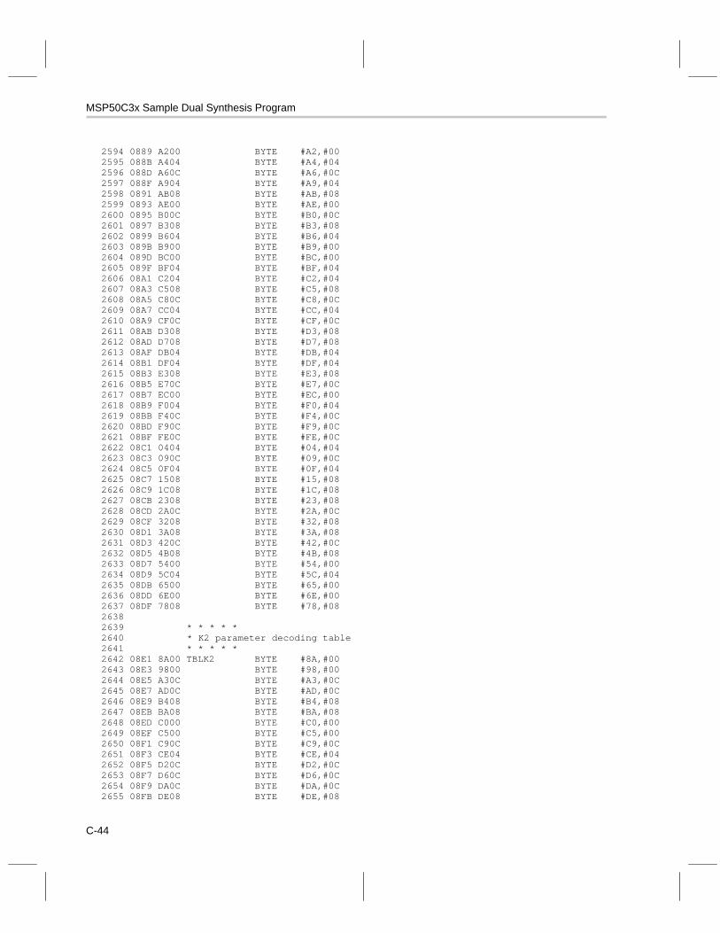
MSP50C3x Sample Dual Synthesis Program
C-44
2594 0889 A200 BYTE #A2,#002595 088B A404 BYTE #A4,#042596 088D A60C BYTE #A6,#0C2597 088F A904 BYTE #A9,#042598 0891 AB08 BYTE #AB,#082599 0893 AE00 BYTE #AE,#002600 0895 B00C BYTE #B0,#0C2601 0897 B308 BYTE #B3,#082602 0899 B604 BYTE #B6,#042603 089B B900 BYTE #B9,#002604 089D BC00 BYTE #BC,#002605 089F BF04 BYTE #BF,#042606 08A1 C204 BYTE #C2,#042607 08A3 C508 BYTE #C5,#082608 08A5 C80C BYTE #C8,#0C2609 08A7 CC04 BYTE #CC,#042610 08A9 CF0C BYTE #CF,#0C2611 08AB D308 BYTE #D3,#082612 08AD D708 BYTE #D7,#082613 08AF DB04 BYTE #DB,#042614 08B1 DF04 BYTE #DF,#042615 08B3 E308 BYTE #E3,#082616 08B5 E70C BYTE #E7,#0C2617 08B7 EC00 BYTE #EC,#002618 08B9 F004 BYTE #F0,#042619 08BB F40C BYTE #F4,#0C2620 08BD F90C BYTE #F9,#0C2621 08BF FE0C BYTE #FE,#0C2622 08C1 0404 BYTE #04,#042623 08C3 090C BYTE #09,#0C2624 08C5 0F04 BYTE #0F,#042625 08C7 1508 BYTE #15,#082626 08C9 1C08 BYTE #1C,#082627 08CB 2308 BYTE #23,#082628 08CD 2A0C BYTE #2A,#0C2629 08CF 3208 BYTE #32,#082630 08D1 3A08 BYTE #3A,#082631 08D3 420C BYTE #42,#0C2632 08D5 4B08 BYTE #4B,#082633 08D7 5400 BYTE #54,#002634 08D9 5C04 BYTE #5C,#042635 08DB 6500 BYTE #65,#002636 08DD 6E00 BYTE #6E,#002637 08DF 7808 BYTE #78,#0826382639 * * * * *2640 * K2 parameter decoding table2641 * * * * *2642 08E1 8A00 TBLK2 BYTE #8A,#002643 08E3 9800 BYTE #98,#002644 08E5 A30C BYTE #A3,#0C2645 08E7 AD0C BYTE #AD,#0C2646 08E9 B408 BYTE #B4,#082647 08EB BA08 BYTE #BA,#082648 08ED C000 BYTE #C0,#002649 08EF C500 BYTE #C5,#002650 08F1 C90C BYTE #C9,#0C2651 08F3 CE04 BYTE #CE,#042652 08F5 D20C BYTE #D2,#0C2653 08F7 D60C BYTE #D6,#0C2654 08F9 DA0C BYTE #DA,#0C2655 08FB DE08 BYTE #DE,#08
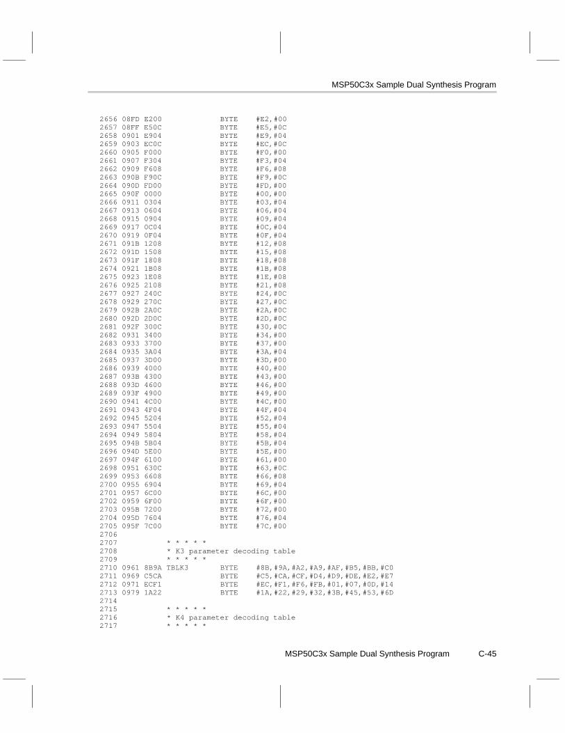
MSP50C3x Sample Dual Synthesis Program
C-45 MSP50C3x Sample Dual Synthesis Program
2656 08FD E200 BYTE #E2,#002657 08FF E50C BYTE #E5,#0C2658 0901 E904 BYTE #E9,#042659 0903 EC0C BYTE #EC,#0C2660 0905 F000 BYTE #F0,#002661 0907 F304 BYTE #F3,#042662 0909 F608 BYTE #F6,#082663 090B F90C BYTE #F9,#0C2664 090D FD00 BYTE #FD,#002665 090F 0000 BYTE #00,#002666 0911 0304 BYTE #03,#042667 0913 0604 BYTE #06,#042668 0915 0904 BYTE #09,#042669 0917 0C04 BYTE #0C,#042670 0919 0F04 BYTE #0F,#042671 091B 1208 BYTE #12,#082672 091D 1508 BYTE #15,#082673 091F 1808 BYTE #18,#082674 0921 1B08 BYTE #1B,#082675 0923 1E08 BYTE #1E,#082676 0925 2108 BYTE #21,#082677 0927 240C BYTE #24,#0C2678 0929 270C BYTE #27,#0C2679 092B 2A0C BYTE #2A,#0C2680 092D 2D0C BYTE #2D,#0C2681 092F 300C BYTE #30,#0C2682 0931 3400 BYTE #34,#002683 0933 3700 BYTE #37,#002684 0935 3A04 BYTE #3A,#042685 0937 3D00 BYTE #3D,#002686 0939 4000 BYTE #40,#002687 093B 4300 BYTE #43,#002688 093D 4600 BYTE #46,#002689 093F 4900 BYTE #49,#002690 0941 4C00 BYTE #4C,#002691 0943 4F04 BYTE #4F,#042692 0945 5204 BYTE #52,#042693 0947 5504 BYTE #55,#042694 0949 5804 BYTE #58,#042695 094B 5B04 BYTE #5B,#042696 094D 5E00 BYTE #5E,#002697 094F 6100 BYTE #61,#002698 0951 630C BYTE #63,#0C2699 0953 6608 BYTE #66,#082700 0955 6904 BYTE #69,#042701 0957 6C00 BYTE #6C,#002702 0959 6F00 BYTE #6F,#002703 095B 7200 BYTE #72,#002704 095D 7604 BYTE #76,#042705 095F 7C00 BYTE #7C,#0027062707 * * * * *2708 * K3 parameter decoding table2709 * * * * *2710 0961 8B9A TBLK3 BYTE #8B,#9A,#A2,#A9,#AF,#B5,#BB,#C02711 0969 C5CA BYTE #C5,#CA,#CF,#D4,#D9,#DE,#E2,#E72712 0971 ECF1 BYTE #EC,#F1,#F6,#FB,#01,#07,#0D,#142713 0979 1A22 BYTE #1A,#22,#29,#32,#3B,#45,#53,#6D27142715 * * * * *2716 * K4 parameter decoding table2717 * * * * *
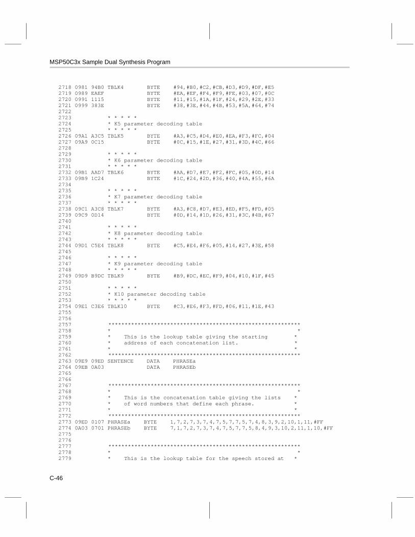
MSP50C3x Sample Dual Synthesis Program
C-46
2718 0981 94B0 TBLK4 BYTE #94,#B0,#C2,#CB,#D3,#D9,#DF,#E52719 0989 EAEF BYTE #EA,#EF,#F4,#F9,#FE,#03,#07,#0C2720 0991 1115 BYTE #11,#15,#1A,#1F,#24,#29,#2E,#332721 0999 383E BYTE #38,#3E,#44,#4B,#53,#5A,#64,#7427222723 * * * * *2724 * K5 parameter decoding table2725 * * * * *2726 09A1 A3C5 TBLK5 BYTE #A3,#C5,#D4,#E0,#EA,#F3,#FC,#042727 09A9 0C15 BYTE #0C,#15,#1E,#27,#31,#3D,#4C,#6627282729 * * * * *2730 * K6 parameter decoding table2731 * * * * *2732 09B1 AAD7 TBLK6 BYTE #AA,#D7,#E7,#F2,#FC,#05,#0D,#142733 09B9 1C24 BYTE #1C,#24,#2D,#36,#40,#4A,#55,#6A27342735 * * * * *2736 * K7 parameter decoding table2737 * * * * *2738 09C1 A3C8 TBLK7 BYTE #A3,#C8,#D7,#E3,#ED,#F5,#FD,#052739 09C9 0D14 BYTE #0D,#14,#1D,#26,#31,#3C,#4B,#6727402741 * * * * *2742 * K8 parameter decoding table2743 * * * * *2744 09D1 C5E4 TBLK8 BYTE #C5,#E4,#F6,#05,#14,#27,#3E,#5827452746 * * * * *2747 * K9 parameter decoding table2748 * * * * *2749 09D9 B9DC TBLK9 BYTE #B9,#DC,#EC,#F9,#04,#10,#1F,#4527502751 * * * * *2752 * K10 parameter decoding table2753 * * * * *2754 09E1 C3E6 TBLK10 BYTE #C3,#E6,#F3,#FD,#06,#11,#1E,#43275527562757 ***********************************************************2758 * *2759 * This is the lookup table giving the starting *2760 * address of each concatenation list. *2761 * *2762 ***********************************************************2763 09E9 09ED SENTENCE DATA PHRASEa2764 09EB 0A03 DATA PHRASEb276527662767 ***********************************************************2768 * *2769 * This is the concatenation table giving the lists *2770 * of word numbers that define each phrase. *2771 * *2772 ***********************************************************2773 09ED 0107 PHRASEa BYTE 1,7,2,7,3,7,4,7,5,7,7,5,7,4,8,3,9,2,10,1,11,#FF2774 0A03 0701 PHRASEb BYTE 7,1,7,2,7,3,7,4,7,5,7,7,5,8,4,9,3,10,2,11,1,10,#FF277527762777 ***********************************************************2778 * *2779 * This is the lookup table for the speech stored at *
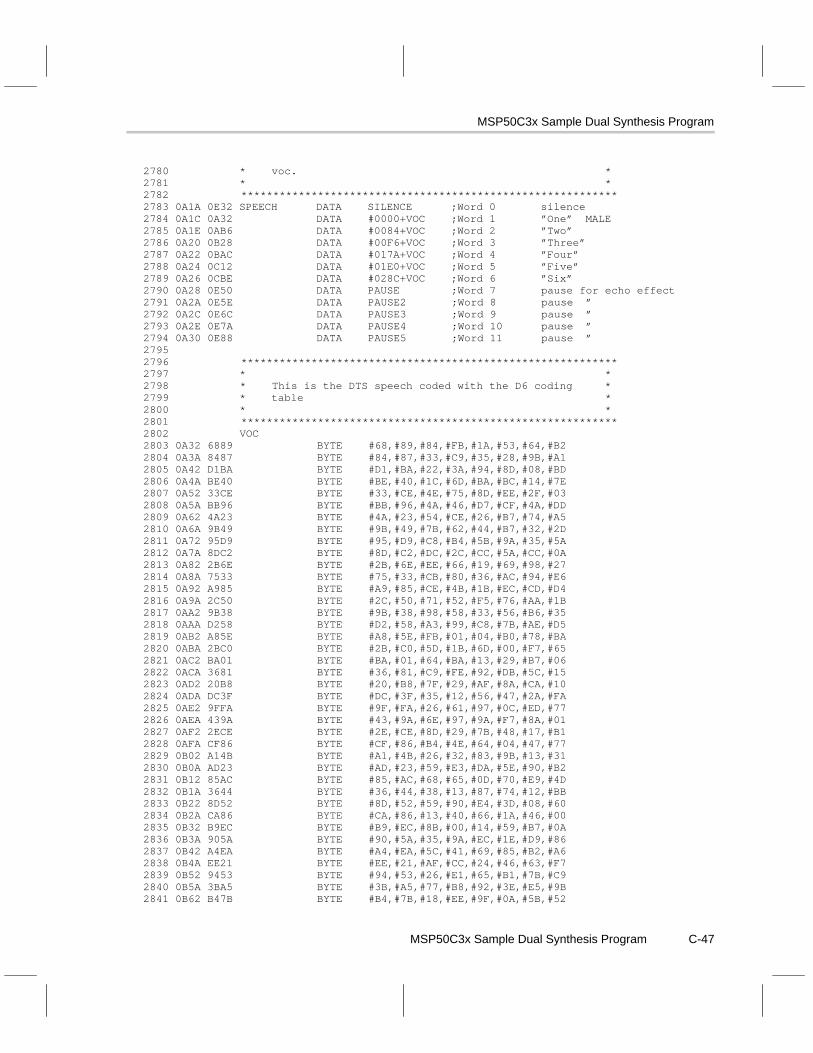
MSP50C3x Sample Dual Synthesis Program
C-47 MSP50C3x Sample Dual Synthesis Program
2780 * voc. *2781 * *2782 ***********************************************************2783 0A1A 0E32 SPEECH DATA SILENCE ;Word 0 silence2784 0A1C 0A32 DATA #0000+VOC ;Word 1 ”One” MALE2785 0A1E 0AB6 DATA #0084+VOC ;Word 2 ”Two”2786 0A20 0B28 DATA #00F6+VOC ;Word 3 ”Three”2787 0A22 0BAC DATA #017A+VOC ;Word 4 ”Four”2788 0A24 0C12 DATA #01E0+VOC ;Word 5 ”Five”2789 0A26 0CBE DATA #028C+VOC ;Word 6 ”Six”2790 0A28 0E50 DATA PAUSE ;Word 7 pause for echo effect2791 0A2A 0E5E DATA PAUSE2 ;Word 8 pause ”2792 0A2C 0E6C DATA PAUSE3 ;Word 9 pause ”2793 0A2E 0E7A DATA PAUSE4 ;Word 10 pause ”2794 0A30 0E88 DATA PAUSE5 ;Word 11 pause ”27952796 ***********************************************************2797 * *2798 * This is the DTS speech coded with the D6 coding *2799 * table *2800 * *2801 ***********************************************************2802 VOC2803 0A32 6889 BYTE #68,#89,#84,#FB,#1A,#53,#64,#B22804 0A3A 8487 BYTE #84,#87,#33,#C9,#35,#28,#9B,#A12805 0A42 D1BA BYTE #D1,#BA,#22,#3A,#94,#8D,#08,#BD2806 0A4A BE40 BYTE #BE,#40,#1C,#6D,#BA,#BC,#14,#7E2807 0A52 33CE BYTE #33,#CE,#4E,#75,#8D,#EE,#2F,#032808 0A5A BB96 BYTE #BB,#96,#4A,#46,#D7,#CF,#4A,#DD2809 0A62 4A23 BYTE #4A,#23,#54,#CE,#26,#B7,#74,#A52810 0A6A 9B49 BYTE #9B,#49,#7B,#62,#44,#B7,#32,#2D2811 0A72 95D9 BYTE #95,#D9,#C8,#B4,#5B,#9A,#35,#5A2812 0A7A 8DC2 BYTE #8D,#C2,#DC,#2C,#CC,#5A,#CC,#0A2813 0A82 2B6E BYTE #2B,#6E,#EE,#66,#19,#69,#98,#272814 0A8A 7533 BYTE #75,#33,#CB,#80,#36,#AC,#94,#E62815 0A92 A985 BYTE #A9,#85,#CE,#4B,#1B,#EC,#CD,#D42816 0A9A 2C50 BYTE #2C,#50,#71,#52,#F5,#76,#AA,#1B2817 0AA2 9B38 BYTE #9B,#38,#98,#58,#33,#56,#B6,#352818 0AAA D258 BYTE #D2,#58,#A3,#99,#C8,#7B,#AE,#D52819 0AB2 A85E BYTE #A8,#5E,#FB,#01,#04,#B0,#78,#BA2820 0ABA 2BC0 BYTE #2B,#C0,#5D,#1B,#6D,#00,#F7,#652821 0AC2 BA01 BYTE #BA,#01,#64,#BA,#13,#29,#B7,#062822 0ACA 3681 BYTE #36,#81,#C9,#FE,#92,#DB,#5C,#152823 0AD2 20B8 BYTE #20,#B8,#7F,#29,#AF,#8A,#CA,#102824 0ADA DC3F BYTE #DC,#3F,#35,#12,#56,#47,#2A,#FA2825 0AE2 9FFA BYTE #9F,#FA,#26,#61,#97,#0C,#ED,#772826 0AEA 439A BYTE #43,#9A,#6E,#97,#9A,#F7,#8A,#012827 0AF2 2ECE BYTE #2E,#CE,#8D,#29,#7B,#48,#17,#B12828 0AFA CF86 BYTE #CF,#86,#B4,#4E,#64,#04,#47,#772829 0B02 A14B BYTE #A1,#4B,#26,#32,#83,#9B,#13,#312830 0B0A AD23 BYTE #AD,#23,#59,#E3,#DA,#5E,#90,#B22831 0B12 85AC BYTE #85,#AC,#68,#65,#0D,#70,#E9,#4D2832 0B1A 3644 BYTE #36,#44,#38,#13,#87,#74,#12,#BB2833 0B22 8D52 BYTE #8D,#52,#59,#90,#E4,#3D,#08,#602834 0B2A CA86 BYTE #CA,#86,#13,#40,#66,#1A,#46,#002835 0B32 B9EC BYTE #B9,#EC,#8B,#00,#14,#59,#B7,#0A2836 0B3A 905A BYTE #90,#5A,#35,#9A,#EC,#1E,#D9,#862837 0B42 A4EA BYTE #A4,#EA,#5C,#41,#69,#85,#B2,#A62838 0B4A EE21 BYTE #EE,#21,#AF,#CC,#24,#46,#63,#F72839 0B52 9453 BYTE #94,#53,#26,#E1,#65,#B1,#7B,#C92840 0B5A 3BA5 BYTE #3B,#A5,#77,#B8,#92,#3E,#E5,#9B2841 0B62 B47B BYTE #B4,#7B,#18,#EE,#9F,#0A,#5B,#52
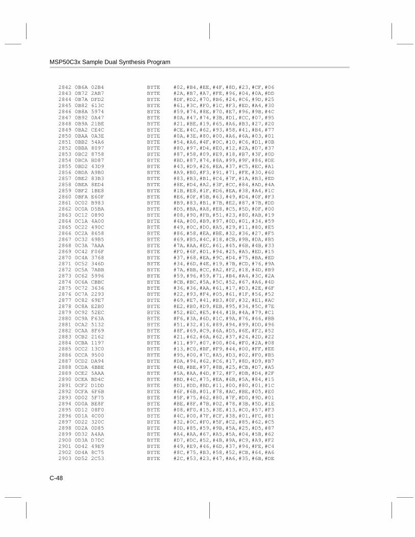
MSP50C3x Sample Dual Synthesis Program
C-48
2842 0B6A 02B4 BYTE #02,#B4,#EE,#4F,#8D,#23,#CF,#062843 0B72 2AB7 BYTE #2A,#B7,#A7,#FE,#96,#04,#0A,#DD2844 0B7A DFD2 BYTE #DF,#D2,#70,#B6,#24,#C6,#9D,#252845 0B82 613C BYTE #61,#3C,#F0,#1C,#F3,#ED,#A4,#302846 0B8A 5974 BYTE #59,#74,#8E,#70,#E7,#96,#9B,#4C2847 0B92 0A47 BYTE #0A,#47,#74,#3B,#D1,#CC,#07,#952848 0B9A 21BE BYTE #21,#BE,#19,#65,#A6,#B3,#27,#202849 0BA2 CE4C BYTE #CE,#4C,#62,#93,#58,#41,#B4,#772850 0BAA 0A3E BYTE #0A,#3E,#80,#00,#A6,#6A,#03,#012851 0BB2 54A6 BYTE #54,#A6,#4F,#0C,#10,#C6,#D1,#0B2852 0BBA 8097 BYTE #80,#97,#D4,#E0,#12,#2A,#D7,#372853 0BC2 8758 BYTE #87,#58,#09,#E9,#18,#B7,#3F,#0D2854 0BCA BD87 BYTE #BD,#87,#74,#8A,#99,#9F,#86,#DE2855 0BD2 43D9 BYTE #43,#D9,#26,#EA,#37,#C5,#EC,#A12856 0BDA A9B0 BYTE #A9,#B0,#F3,#91,#71,#FE,#30,#602857 0BE2 83B3 BYTE #83,#B3,#B1,#C4,#7F,#1A,#B3,#ED2858 0BEA 8ED4 BYTE #8E,#D4,#A2,#3F,#CC,#84,#AD,#4A2859 0BF2 1BE8 BYTE #1B,#E8,#1F,#D6,#EA,#38,#A4,#1C2860 0BFA E60F BYTE #E6,#0F,#5B,#63,#49,#D4,#0F,#F32861 0C02 B983 BYTE #B9,#83,#B1,#7B,#E2,#87,#7B,#DD2862 0C0A D5BA BYTE #D5,#BA,#A8,#E8,#C5,#5D,#0F,#002863 0C12 0890 BYTE #08,#90,#FB,#51,#23,#80,#AB,#192864 0C1A 4A00 BYTE #4A,#00,#B9,#97,#0D,#01,#34,#592865 0C22 490C BYTE #49,#0C,#D0,#A5,#29,#11,#80,#E52866 0C2A 8658 BYTE #86,#58,#EA,#BE,#32,#36,#27,#F52867 0C32 69B5 BYTE #69,#B5,#4C,#18,#CB,#9B,#DA,#B52868 0C3A 7AAA BYTE #7A,#AA,#EC,#61,#45,#6B,#4B,#332869 0C42 F06F BYTE #F0,#6F,#D1,#94,#25,#A5,#ED,#152870 0C4A 3768 BYTE #37,#68,#EA,#9C,#D4,#75,#BA,#ED2871 0C52 346D BYTE #34,#6D,#4E,#19,#7B,#CD,#76,#9A2872 0C5A 7ABB BYTE #7A,#BB,#CC,#A2,#F2,#18,#4D,#B92873 0C62 5996 BYTE #59,#96,#59,#71,#B4,#A4,#3C,#2A2874 0C6A CBBC BYTE #CB,#BC,#5A,#5C,#52,#67,#A6,#4D2875 0C72 3636 BYTE #36,#36,#AA,#61,#17,#D3,#2E,#6F2876 0C7A 2293 BYTE #22,#93,#F4,#05,#61,#1F,#56,#522877 0C82 69E7 BYTE #69,#E7,#41,#B3,#0F,#32,#E1,#AC2878 0C8A E2B0 BYTE #E2,#B0,#D9,#EB,#95,#34,#5C,#7E2879 0C92 52EC BYTE #52,#EC,#E5,#44,#1B,#4A,#79,#C12880 0C9A F63A BYTE #F6,#3A,#6D,#1C,#9A,#76,#66,#BB2881 0CA2 5132 BYTE #51,#32,#16,#89,#94,#99,#DD,#962882 0CAA 8F69 BYTE #8F,#69,#C9,#6A,#D5,#6E,#F2,#522883 0CB2 2162 BYTE #21,#62,#6A,#62,#37,#24,#2D,#222884 0CBA 1197 BYTE #11,#97,#07,#00,#04,#F0,#2A,#082885 0CC2 13C0 BYTE #13,#C0,#BF,#F9,#44,#00,#FF,#EE2886 0CCA 9500 BYTE #95,#00,#7C,#A5,#D3,#02,#F0,#B52887 0CD2 DA94 BYTE #DA,#94,#62,#C6,#17,#8D,#D9,#B72888 0CDA 4BBE BYTE #4B,#BE,#97,#8B,#25,#CB,#D7,#A52889 0CE2 5AAA BYTE #5A,#AA,#4D,#72,#F7,#DB,#D4,#2F2890 0CEA BD4C BYTE #BD,#4C,#75,#EA,#6B,#5A,#84,#152891 0CF2 D1DD BYTE #D1,#DD,#BD,#11,#00,#80,#01,#1C2892 0CFA 6F6B BYTE #6F,#6B,#01,#78,#AC,#BE,#05,#E02893 0D02 5F75 BYTE #5F,#75,#62,#80,#7F,#D0,#9D,#012894 0D0A BE8F BYTE #BE,#8F,#7B,#02,#78,#3B,#5D,#1E2895 0D12 08F0 BYTE #08,#F0,#15,#3E,#13,#C0,#57,#F32896 0D1A 4C00 BYTE #4C,#00,#7F,#CF,#38,#01,#FC,#812897 0D22 320C BYTE #32,#0C,#F0,#5F,#C2,#85,#62,#C52898 0D2A 0D85 BYTE #0D,#85,#59,#9B,#5A,#25,#D5,#872899 0D32 A4AA BYTE #A4,#AA,#67,#A5,#5A,#04,#5B,#622900 0D3A D7DC BYTE #D7,#DC,#52,#4B,#9A,#C9,#A9,#F22901 0D42 49E9 BYTE #49,#E9,#46,#6D,#37,#94,#FE,#C42902 0D4A 8C75 BYTE #8C,#75,#B3,#58,#52,#CB,#64,#A62903 0D52 2C53 BYTE #2C,#53,#23,#47,#A6,#35,#6B,#DE
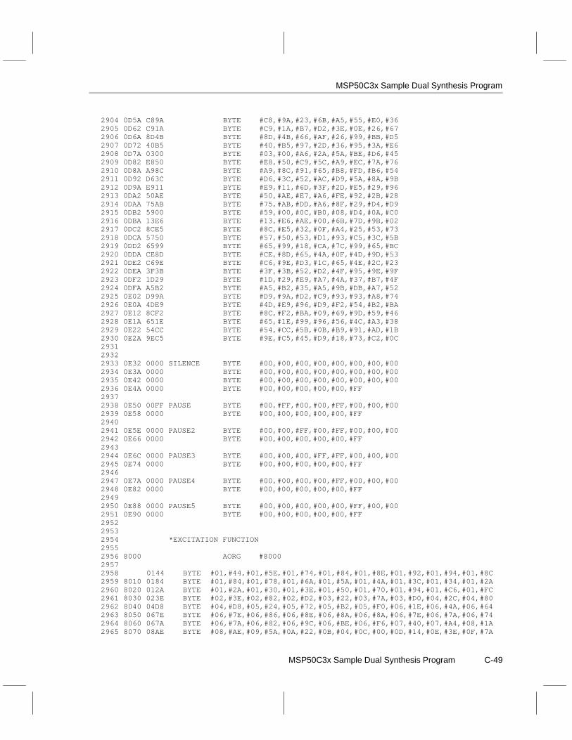
MSP50C3x Sample Dual Synthesis Program
C-49 MSP50C3x Sample Dual Synthesis Program
2904 0D5A C89A BYTE #C8,#9A,#23,#6B,#A5,#55,#E0,#362905 0D62 C91A BYTE #C9,#1A,#B7,#D2,#3E,#0E,#26,#672906 0D6A 8D4B BYTE #8D,#4B,#66,#AF,#26,#99,#BB,#D52907 0D72 40B5 BYTE #40,#B5,#97,#2D,#36,#95,#3A,#E62908 0D7A 0300 BYTE #03,#00,#A6,#2A,#5A,#BE,#D6,#452909 0D82 E850 BYTE #E8,#50,#C9,#5C,#A9,#EC,#7A,#762910 0D8A A98C BYTE #A9,#8C,#91,#65,#B8,#FD,#B6,#542911 0D92 D63C BYTE #D6,#3C,#52,#AC,#D9,#5A,#8A,#9B2912 0D9A E911 BYTE #E9,#11,#6D,#3F,#2D,#E5,#29,#962913 0DA2 50AE BYTE #50,#AE,#E7,#A6,#FE,#92,#2B,#282914 0DAA 75AB BYTE #75,#AB,#DD,#A6,#8F,#29,#D4,#D92915 0DB2 5900 BYTE #59,#00,#0C,#B0,#08,#D4,#0A,#C02916 0DBA 13E6 BYTE #13,#E6,#AE,#00,#6B,#7D,#9B,#022917 0DC2 8CE5 BYTE #8C,#E5,#32,#0F,#A4,#25,#53,#732918 0DCA 5750 BYTE #57,#50,#53,#D1,#93,#C5,#3C,#5B2919 0DD2 6599 BYTE #65,#99,#18,#CA,#7C,#99,#65,#BC2920 0DDA CE8D BYTE #CE,#8D,#65,#4A,#0F,#4D,#9D,#532921 0DE2 C69E BYTE #C6,#9E,#D3,#1C,#65,#4E,#2C,#232922 0DEA 3F3B BYTE #3F,#3B,#52,#D2,#4F,#95,#9E,#9F2923 0DF2 1D29 BYTE #1D,#29,#E9,#A7,#4A,#37,#B7,#4F2924 0DFA A5B2 BYTE #A5,#B2,#35,#A5,#9B,#DB,#A7,#522925 0E02 D99A BYTE #D9,#9A,#D2,#C9,#93,#93,#A8,#742926 0E0A 4DE9 BYTE #4D,#E9,#96,#D9,#F2,#54,#B2,#BA2927 0E12 8CF2 BYTE #8C,#F2,#BA,#09,#69,#9D,#59,#462928 0E1A 651E BYTE #65,#1E,#99,#96,#56,#4C,#A3,#382929 0E22 54CC BYTE #54,#CC,#5B,#0B,#B9,#91,#AD,#1B2930 0E2A 9EC5 BYTE #9E,#C5,#45,#D9,#18,#73,#C2,#0C293129322933 0E32 0000 SILENCE BYTE #00,#00,#00,#00,#00,#00,#00,#002934 0E3A 0000 BYTE #00,#00,#00,#00,#00,#00,#00,#002935 0E42 0000 BYTE #00,#00,#00,#00,#00,#00,#00,#002936 0E4A 0000 BYTE #00,#00,#00,#00,#00,#FF29372938 0E50 00FF PAUSE BYTE #00,#FF,#00,#00,#FF,#00,#00,#002939 0E58 0000 BYTE #00,#00,#00,#00,#00,#FF29402941 0E5E 0000 PAUSE2 BYTE #00,#00,#FF,#00,#FF,#00,#00,#002942 0E66 0000 BYTE #00,#00,#00,#00,#00,#FF29432944 0E6C 0000 PAUSE3 BYTE #00,#00,#00,#FF,#FF,#00,#00,#002945 0E74 0000 BYTE #00,#00,#00,#00,#00,#FF29462947 0E7A 0000 PAUSE4 BYTE #00,#00,#00,#00,#FF,#00,#00,#002948 0E82 0000 BYTE #00,#00,#00,#00,#00,#FF29492950 0E88 0000 PAUSE5 BYTE #00,#00,#00,#00,#00,#FF,#00,#002951 0E90 0000 BYTE #00,#00,#00,#00,#00,#FF295229532954 *EXCITATION FUNCTION29552956 8000 AORG #800029572958 0144 BYTE #01,#44,#01,#5E,#01,#74,#01,#84,#01,#8E,#01,#92,#01,#94,#01,#8C2959 8010 0184 BYTE #01,#84,#01,#78,#01,#6A,#01,#5A,#01,#4A,#01,#3C,#01,#34,#01,#2A2960 8020 012A BYTE #01,#2A,#01,#30,#01,#3E,#01,#50,#01,#70,#01,#94,#01,#C6,#01,#FC2961 8030 023E BYTE #02,#3E,#02,#82,#02,#D2,#03,#22,#03,#7A,#03,#D0,#04,#2C,#04,#802962 8040 04D8 BYTE #04,#D8,#05,#24,#05,#72,#05,#B2,#05,#F0,#06,#1E,#06,#4A,#06,#642963 8050 067E BYTE #06,#7E,#06,#86,#06,#8E,#06,#8A,#06,#8A,#06,#7E,#06,#7A,#06,#742964 8060 067A BYTE #06,#7A,#06,#82,#06,#9C,#06,#BE,#06,#F6,#07,#40,#07,#A4,#08,#1A2965 8070 08AE BYTE #08,#AE,#09,#5A,#0A,#22,#0B,#04,#0C,#00,#0D,#14,#0E,#3E,#0F,#7A
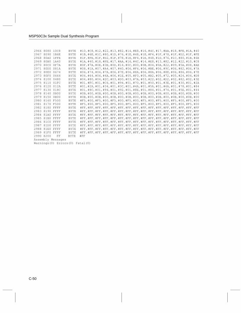
MSP50C3x Sample Dual Synthesis Program
C-50
2966 8080 10C8 BYTE #10,#C8,#12,#22,#13,#82,#14,#E8,#16,#4C,#17,#AA,#18,#FE,#1A,#402967 8090 1B6E BYTE #1B,#6E,#1C,#80,#1D,#76,#1E,#48,#1E,#F4,#1F,#78,#1F,#D2,#1F,#FE2968 80A0 1FFE BYTE #1F,#FE,#1F,#D2,#1F,#78,#1E,#F4,#1E,#48,#1D,#76,#1C,#80,#1B,#6E2969 80B0 1A40 BYTE #1A,#40,#18,#FE,#17,#AA,#16,#4C,#14,#E8,#13,#82,#12,#22,#10,#C82970 80C0 0F7A BYTE #0F,#7A,#0E,#3E,#0D,#14,#0C,#00,#0B,#04,#0A,#22,#09,#5A,#08,#AE2971 80D0 081A BYTE #08,#1A,#07,#A4,#07,#40,#06,#F6,#06,#BE,#06,#9C,#06,#82,#06,#7A2972 80E0 0674 BYTE #06,#74,#06,#7A,#06,#7E,#06,#8A,#06,#8A,#06,#8E,#06,#86,#06,#7E2973 80F0 0664 BYTE #06,#64,#06,#4A,#06,#1E,#05,#F0,#05,#B2,#05,#72,#05,#24,#04,#D82974 8100 0480 BYTE #04,#80,#04,#2C,#03,#D0,#03,#7A,#03,#22,#02,#D2,#02,#82,#02,#3E2975 8110 01FC BYTE #01,#FC,#01,#C6,#01,#94,#01,#70,#01,#50,#01,#3E,#01,#30,#01,#2A2976 8120 012A BYTE #01,#2A,#01,#34,#01,#3C,#01,#4A,#01,#5A,#01,#6A,#01,#78,#01,#842977 8130 018C BYTE #01,#8C,#01,#94,#01,#92,#01,#8E,#01,#84,#01,#74,#01,#5E,#01,#442978 8140 0B00 BYTE #0B,#00,#0B,#00,#0B,#00,#0B,#00,#0B,#00,#0B,#00,#0B,#00,#0B,#002979 8150 0B00 BYTE #0B,#00,#0B,#00,#0B,#00,#0B,#00,#0B,#00,#0B,#00,#0B,#00,#0B,#002980 8160 F500 BYTE #F5,#00,#F5,#00,#F5,#00,#F5,#00,#F5,#00,#F5,#00,#F5,#00,#F5,#002981 8170 F500 BYTE #F5,#00,#F5,#00,#F5,#00,#F5,#00,#F5,#00,#F5,#00,#F5,#00,#F5,#002982 8180 FFFF BYTE #FF,#FF,#FF,#FF,#FF,#FF,#FF,#FF,#FF,#FF,#FF,#FF,#FF,#FF,#FF,#FF2983 8190 FFFF BYTE #FF,#FF,#FF,#FF,#FF,#FF,#FF,#FF,#FF,#FF,#FF,#FF,#FF,#FF,#FF,#FF2984 81A0 FFFF BYTE #FF,#FF,#FF,#FF,#FF,#FF,#FF,#FF,#FF,#FF,#FF,#FF,#FF,#FF,#FF,#FF2985 81B0 FFFF BYTE #FF,#FF,#FF,#FF,#FF,#FF,#FF,#FF,#FF,#FF,#FF,#FF,#FF,#FF,#FF,#FF2986 81C0 FFFF BYTE #FF,#FF,#FF,#FF,#FF,#FF,#FF,#FF,#FF,#FF,#FF,#FF,#FF,#FF,#FF,#FF2987 81D0 FFFF BYTE #FF,#FF,#FF,#FF,#FF,#FF,#FF,#FF,#FF,#FF,#FF,#FF,#FF,#FF,#FF,#FF2988 81E0 FFFF BYTE #FF,#FF,#FF,#FF,#FF,#FF,#FF,#FF,#FF,#FF,#FF,#FF,#FF,#FF,#FF,#FF2989 81F0 FFFF BYTE #FF,#FF,#FF,#FF,#FF,#FF,#FF,#FF,#FF,#FF,#FF,#FF,#FF,#FF,#FF,#FF2990 8200 FF BYTE #FFAssembly MessagesWarnings(0) Errors(0) Fatal(0)
D-1
Appendix A
Sample Synthesis Program
This appendix contains the code for a sample synthesis program that runs onthe MSP50C3x family of speech synthesizers. It has the MSP50C3x devicespeak the numbers from one to five on one channel only.
Topic Page
D.1 Sample Synthesis Program D-2. . . . . . . . . . . . . . . . . . . . . . . . . . . . . . . . . . . .
Appendix D
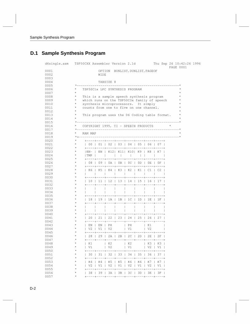
Sample Synthesis Program
D-2
D.1 Sample Synthesis Program
d6single.asm TSP50CXX Assembler Version 2.1d Thu Sep 26 10:42:26 1996 PAGE 00010001 OPTION BUNLIST,DUNLIST,PAGEOF0002 WIDE00030004 TABSIZE 80005 *––––––––––––––––––––––––––––––––––––––––––––––––––––*0006 * TSP50C1x LPC SYNTHESIS PROGRAM *0007 * *0008 * This is a sample speech synthesis program *0009 * which runs on the TSP50C3x family of speech *0010 * synthesis microprocessors. It simply *0011 * counts from one to five on one channel. *0012 * *0013 * This program uses the D6 Coding table format. *0014 * *0015 *––––––––––––––––––––––––––––––––––––––––––––––––––––*0016 * COPYRIGHT 1995, TI – SPEECH PRODUCTS *0017 *––––––––––––––––––––––––––––––––––––––––––––––––––––*0018 * RAM MAP *0019 *+–––––––––––––––––––––––––––––––––––––––––––––––––––*0020 * +––––+––––+––––+––––+––––+––––+––––+––––+0021 * | 00 | 01 | 02 | 03 | 04 | 05 | 06 | 07 |0022 * +––––+––––+––––+––––+––––+––––+––––+––––+0023 * |EN– | EN | K12| K11| K10| K9 | K8 | K7 |0024 * |TMP | | | | | | | | |0025 * +––––+––––+––––+––––+––––+––––+––––+––––+0026 * | 08 | 09 | 0A | 0B | 0C | 0D | 0E | 0F |0027 * +––––+––––+––––+––––+––––+––––+––––+––––+0028 * | K6 | K5 | K4 | K3 | K2 | K1 | C1 | C2 |0029 * | | | | | | | | |0030 * +––––+––––+––––+––––+––––+––––+––––+––––+0031 * | 10 | 11 | 12 | 13 | 14 | 15 | 16 | 17 |0032 * +––––+––––+––––+––––+––––+––––+––––+––––+0033 * | | | | | | | | |0034 * | | | | | | | | |0035 * +––––+––––+––––+––––+––––+––––+––––+––––+0036 * | 18 | 19 | 1A | 1B | 1C | 1D | 1E | 1F |0037 * +––––+––––+––––+––––+––––+––––+––––+––––+0038 * | | | | | | | | |0039 * | | | | | | | | |0040 * +––––+––––+––––+––––+––––+––––+––––+––––+0041 * | 20 | 21 | 22 | 23 | 24 | 25 | 26 | 27 |0042 * +––––+––––+––––+––––+––––+––––+––––+––––+0043 * | EN | EN | PH | PH | K1 |0044 * | V2 | V1 | V2 | V1 | V2 |0045 * +––––+––––+––––+––––+––––+––––+––––+––––+0046 * | 28 | 29 | 2A | 2B | 2C | 2D | 2E | 2F |0047 * +––––+––––+––––+––––+––––+––––+––––+––––+0048 * | K1 | K2 | K2 | K3 | K3 |0049 * | V1 | V2 | V1 | V2 | V1 |0050 * +––––+––––+––––+––––+––––+––––+––––+––––+0051 * | 30 | 31 | 32 | 33 | 34 | 35 | 36 | 37 |0052 * +––––+––––+––––+––––+––––+––––+––––+––––+0053 * | K4 | K4 | K5 | K5 | K6 | K6 | K7 | K7 |0054 * | V2 | V1 | V2 | V1 | V2 | V1 | V2 | V1 |0055 * +––––+––––+––––+––––+––––+––––+––––+––––+0056 * | 38 | 39 | 3A | 3B | 3C | 3D | 3E | 3F |0057 * +––––+––––+––––+––––+––––+––––+––––+––––+
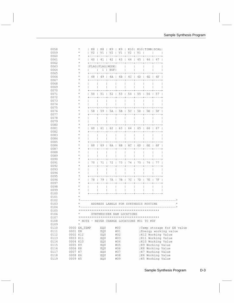
Sample Synthesis Program
D-3 Sample Synthesis Program
0058 * | K8 | K8 | K9 | K9 | K10| K10|TIMR|SCAL|0059 * | V2 | V1 | V2 | V1 | V2 | V1 | | |0060 * +––––+––––+––––+––––+––––+––––+––––+––––+0061 * | 40 | 41 | 42 | 43 | 44 | 45 | 46 | 47 |0062 * +––––+––––+––––+––––+––––+––––+––––+––––+0063 * |FLAG|FLAG|MODE| | | | | |0064 * | | 1 | BUF| | | | | |0065 * +––––+––––+––––+––––+––––+––––+––––+––––+0066 * | 48 | 49 | 4A | 4B | 4C | 4D | 4E | 4F |0067 * +––––+––––+––––+––––+––––+––––+––––+––––+0068 * | | | | | | | | |0069 * | | | | | | | | |0070 * +––––+––––+––––+––––+––––+––––+––––+––––+0071 * | 50 | 51 | 52 | 53 | 54 | 55 | 56 | 57 |0072 * +––––+––––+––––+––––+––––+––––+––––+––––+0073 * | | | | | | | | |0074 * | | | | | | | | |0075 * +––––+––––+––––+––––+––––+––––+––––+––––+0076 * | 58 | 59 | 5A | 5B | 5C | 5D | 5E | 5F |0077 * +––––+––––+––––+––––+––––+––––+––––+––––+0078 * | | | | | | | | |0079 * | | | | | | | | |0080 * +––––+––––+––––+––––+––––+––––+––––+––––+0081 * | 60 | 61 | 62 | 63 | 64 | 65 | 66 | 67 |0082 * +––––+––––+––––+––––+––––+––––+––––+––––+0083 * | | | | | | | | |0084 * | | | | | | | | |0085 * +––––+––––+––––+––––+––––+––––+––––+––––+0086 * | 68 | 69 | 6A | 6B | 6C | 6D | 6E | 6F |0087 * +––––+––––+––––+––––+––––+––––+––––+––––+0088 * | | | | | | | | |0089 * | | | | | | | | |0090 * +––––+––––+––––+––––+––––+––––+––––+––––+0091 * | 70 | 71 | 72 | 73 | 74 | 75 | 76 | 77 |0092 * +––––+––––+––––+––––+––––+––––+––––+––––+0093 * | | | | | | | | |0094 * | | | | | | | | |0095 * +––––+––––+––––+––––+––––+––––+––––+––––+0096 * | 78 | 79 | 7A | 7B | 7C | 7D | 7E | 7F |0097 * +––––+––––+––––+––––+––––+––––+––––+––––+0098 * | | | | | | | | |0099 * | | | | | | | | |0100 * +––––+––––+––––+––––+––––+––––+––––+––––+0101 *0102 *––––––––––––––––––––––––––––––––––––––––––––––––––––*0103 * ADDRESS LABELS FOR SYNTHESIS ROUTINE *0104 *––––––––––––––––––––––––––––––––––––––––––––––––––––*0105 ********************************************0106 * SYNTHESIZER RAM LOCATIONS0107 ********************************************0108 * NOTE – NEVER CHANGE LOCATIONS #01 TO #0F0109 *0110 0000 EN_TEMP EQU #00 ;Temp storage for EN value0111 0001 EN EQU #01 ;Energy working value0112 0002 K12 EQU #02 ;K12 Working Value0113 0003 K11 EQU #03 ;K11 Working Value0114 0004 K10 EQU #04 ;K10 Working Value0115 0005 K9 EQU #05 ;K9 Working Value0116 0006 K8 EQU #06 ;K8 Working Value0117 0007 K7 EQU #07 ;K7 Working Value0118 0008 K6 EQU #08 ;K6 Working Value0119 0009 K5 EQU #09 ;K5 Working Value
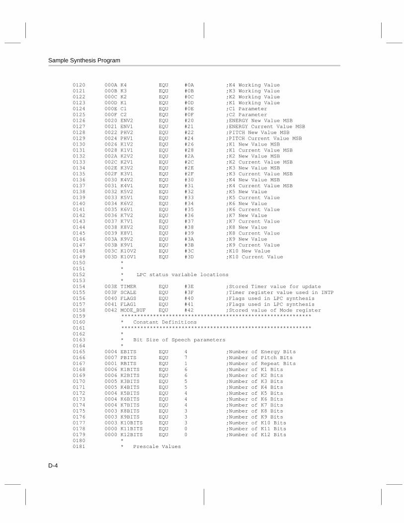
Sample Synthesis Program
D-4
0120 000A K4 EQU #0A ;K4 Working Value0121 000B K3 EQU #0B ;K3 Working Value0122 000C K2 EQU #0C ;K2 Working Value0123 000D K1 EQU #0D ;K1 Working Value0124 000E C1 EQU #0E ;C1 Parameter0125 000F C2 EQU #0F ;C2 Parameter0126 0020 ENV2 EQU #20 ;ENERGY New Value MSB0127 0021 ENV1 EQU #21 ;ENERGY Current Value MSB0128 0022 PHV2 EQU #22 ;PITCH New Value MSB0129 0024 PHV1 EQU #24 ;PITCH Current Value MSB0130 0026 K1V2 EQU #26 ;K1 New Value MSB0131 0028 K1V1 EQU #28 ;K1 Current Value MSB0132 002A K2V2 EQU #2A ;K2 New Value MSB0133 002C K2V1 EQU #2C ;K2 Current Value MSB0134 002E K3V2 EQU #2E ;K3 New Value MSB0135 002F K3V1 EQU #2F ;K3 Current Value MSB0136 0030 K4V2 EQU #30 ;K4 New Value MSB0137 0031 K4V1 EQU #31 ;K4 Current Value MSB0138 0032 K5V2 EQU #32 ;K5 New Value0139 0033 K5V1 EQU #33 ;K5 Current Value0140 0034 K6V2 EQU #34 ;K6 New Value0141 0035 K6V1 EQU #35 ;K6 Current Value0142 0036 K7V2 EQU #36 ;K7 New Value0143 0037 K7V1 EQU #37 ;K7 Current Value0144 0038 K8V2 EQU #38 ;K8 New Value0145 0039 K8V1 EQU #39 ;K8 Current Value0146 003A K9V2 EQU #3A ;K9 New Value0147 003B K9V1 EQU #3B ;K9 Current Value0148 003C K10V2 EQU #3C ;K10 New Value0149 003D K10V1 EQU #3D ;K10 Current Value0150 *0151 *0152 * LPC status variable locations0153 *0154 003E TIMER EQU #3E ;Stored Timer value for update0155 003F SCALE EQU #3F ;Timer register value used in INTP0156 0040 FLAGS EQU #40 ;Flags used in LPC synthesis0157 0041 FLAG1 EQU #41 ;Flags used in LPC synthesis0158 0042 MODE_BUF EQU #42 ;Stored value of Mode register0159 ************************************************************0160 * Constant Definitions0161 ************************************************************0162 *0163 * Bit Size of Speech parameters0164 *0165 0004 EBITS EQU 4 ;Number of Energy Bits0166 0007 PBITS EQU 7 ;Number of Pitch Bits0167 0001 RBITS EQU 1 ;Number of Repeat Bits0168 0006 K1BITS EQU 6 ;Number of K1 Bits0169 0006 K2BITS EQU 6 ;Number of K2 Bits0170 0005 K3BITS EQU 5 ;Number of K3 Bits0171 0005 K4BITS EQU 5 ;Number of K4 Bits0172 0004 K5BITS EQU 4 ;Number of K5 Bits0173 0004 K6BITS EQU 4 ;Number of K6 Bits0174 0004 K7BITS EQU 4 ;Number of K7 Bits0175 0003 K8BITS EQU 3 ;Number of K8 Bits0176 0003 K9BITS EQU 3 ;Number of K9 Bits0177 0003 K10BITS EQU 3 ;Number of K10 Bits0178 0000 K11BITS EQU 0 ;Number of K11 Bits0179 0000 K12BITS EQU 0 ;Number of K12 Bits0180 *0181 * Prescale Values
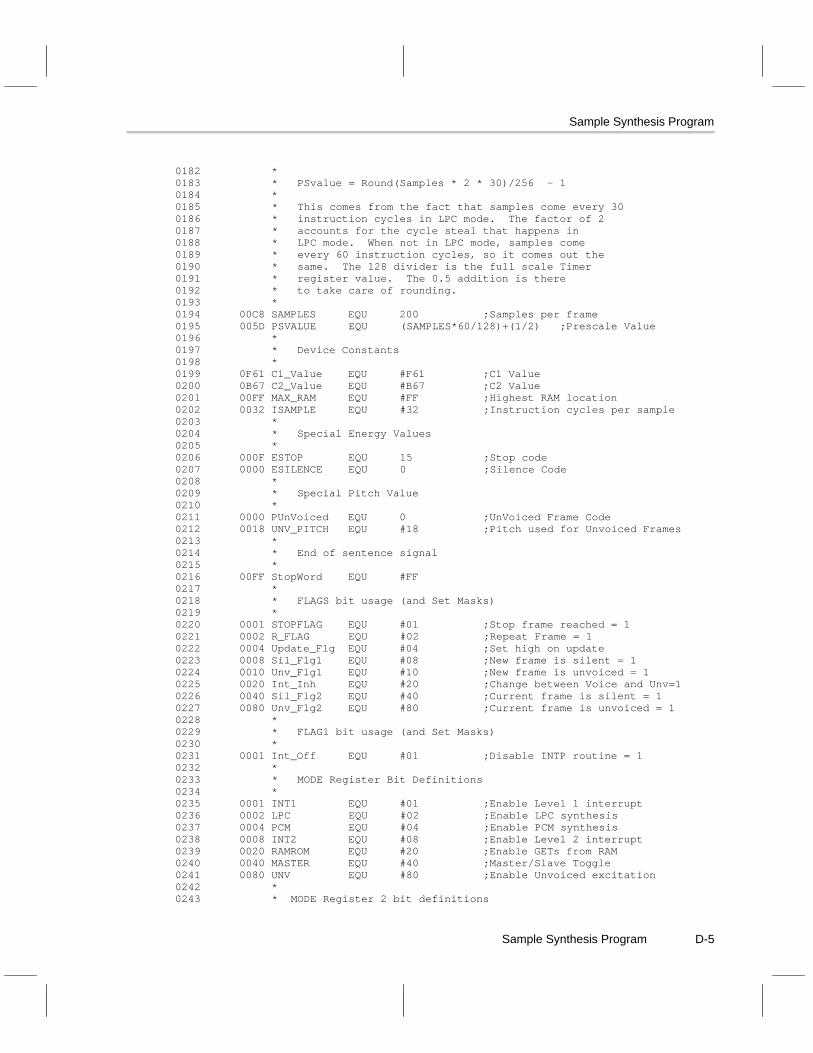
Sample Synthesis Program
D-5 Sample Synthesis Program
0182 *0183 * PSvalue = Round(Samples * 2 * 30)/256 – 10184 *0185 * This comes from the fact that samples come every 300186 * instruction cycles in LPC mode. The factor of 20187 * accounts for the cycle steal that happens in0188 * LPC mode. When not in LPC mode, samples come0189 * every 60 instruction cycles, so it comes out the0190 * same. The 128 divider is the full scale Timer0191 * register value. The 0.5 addition is there0192 * to take care of rounding.0193 *0194 00C8 SAMPLES EQU 200 ;Samples per frame0195 005D PSVALUE EQU (SAMPLES*60/128)+(1/2) ;Prescale Value0196 *0197 * Device Constants0198 *0199 0F61 C1_Value EQU #F61 ;C1 Value0200 0B67 C2_Value EQU #B67 ;C2 Value0201 00FF MAX_RAM EQU #FF ;Highest RAM location0202 0032 ISAMPLE EQU #32 ;Instruction cycles per sample0203 *0204 * Special Energy Values0205 *0206 000F ESTOP EQU 15 ;Stop code0207 0000 ESILENCE EQU 0 ;Silence Code0208 *0209 * Special Pitch Value0210 *0211 0000 PUnVoiced EQU 0 ;UnVoiced Frame Code0212 0018 UNV_PITCH EQU #18 ;Pitch used for Unvoiced Frames0213 *0214 * End of sentence signal0215 *0216 00FF StopWord EQU #FF0217 *0218 * FLAGS bit usage (and Set Masks)0219 *0220 0001 STOPFLAG EQU #01 ;Stop frame reached = 10221 0002 R_FLAG EQU #02 ;Repeat Frame = 10222 0004 Update_Flg EQU #04 ;Set high on update0223 0008 Sil_Flg1 EQU #08 ;New frame is silent = 10224 0010 Unv_Flg1 EQU #10 ;New frame is unvoiced = 10225 0020 Int_Inh EQU #20 ;Change between Voice and Unv=10226 0040 Sil_Flg2 EQU #40 ;Current frame is silent = 10227 0080 Unv_Flg2 EQU #80 ;Current frame is unvoiced = 10228 *0229 * FLAG1 bit usage (and Set Masks)0230 *0231 0001 Int_Off EQU #01 ;Disable INTP routine = 10232 *0233 * MODE Register Bit Definitions0234 *0235 0001 INT1 EQU #01 ;Enable Level 1 interrupt0236 0002 LPC EQU #02 ;Enable LPC synthesis0237 0004 PCM EQU #04 ;Enable PCM synthesis0238 0008 INT2 EQU #08 ;Enable Level 2 interrupt0239 0020 RAMROM EQU #20 ;Enable GETs from RAM0240 0040 MASTER EQU #40 ;Master/Slave Toggle0241 0080 UNV EQU #80 ;Enable Unvoiced excitation0242 *0243 * MODE Register 2 bit definitions
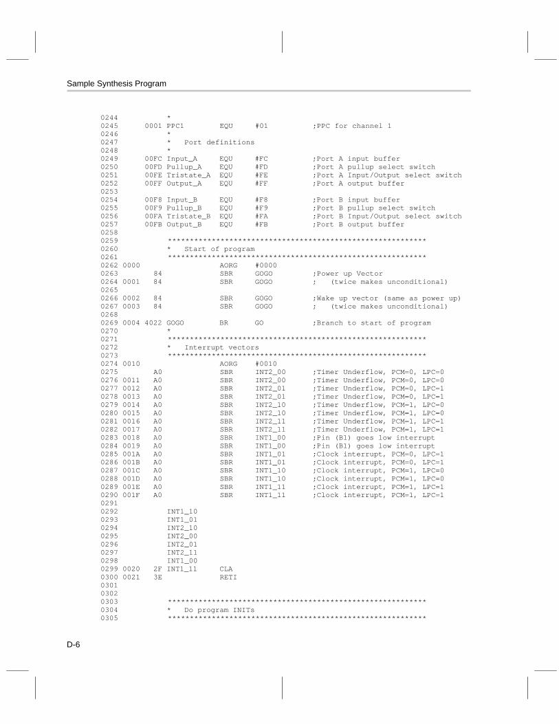
Sample Synthesis Program
D-6
0244 *0245 0001 PPC1 EQU #01 ;PPC for channel 10246 *0247 * Port definitions0248 *0249 00FC Input_A EQU #FC ;Port A input buffer0250 00FD Pullup_A EQU #FD ;Port A pullup select switch0251 00FE Tristate_A EQU #FE ;Port A Input/Output select switch0252 00FF Output_A EQU #FF ;Port A output buffer02530254 00F8 Input_B EQU #F8 ;Port B input buffer0255 00F9 Pullup_B EQU #F9 ;Port B pullup select switch0256 00FA Tristate_B EQU #FA ;Port B Input/Output select switch0257 00FB Output_B EQU #FB ;Port B output buffer02580259 ***********************************************************0260 * Start of program0261 ***********************************************************0262 0000 AORG #00000263 84 SBR GOGO ;Power up Vector0264 0001 84 SBR GOGO ; (twice makes unconditional)02650266 0002 84 SBR GOGO ;Wake up vector (same as power up)0267 0003 84 SBR GOGO ; (twice makes unconditional)02680269 0004 4022 GOGO BR GO ;Branch to start of program0270 *0271 ***********************************************************0272 * Interrupt vectors0273 ***********************************************************0274 0010 AORG #00100275 A0 SBR INT2_00 ;Timer Underflow, PCM=0, LPC=00276 0011 A0 SBR INT2_00 ;Timer Underflow, PCM=0, LPC=00277 0012 A0 SBR INT2_01 ;Timer Underflow, PCM=0, LPC=10278 0013 A0 SBR INT2_01 ;Timer Underflow, PCM=0, LPC=10279 0014 A0 SBR INT2_10 ;Timer Underflow, PCM=1, LPC=00280 0015 A0 SBR INT2_10 ;Timer Underflow, PCM=1, LPC=00281 0016 A0 SBR INT2_11 ;Timer Underflow, PCM=1, LPC=10282 0017 A0 SBR INT2_11 ;Timer Underflow, PCM=1, LPC=10283 0018 A0 SBR INT1_00 ;Pin (B1) goes low interrupt0284 0019 A0 SBR INT1_00 ;Pin (B1) goes low interrupt0285 001A A0 SBR INT1_01 ;Clock interrupt, PCM=0, LPC=10286 001B A0 SBR INT1_01 ;Clock interrupt, PCM=0, LPC=10287 001C A0 SBR INT1_10 ;Clock interrupt, PCM=1, LPC=00288 001D A0 SBR INT1_10 ;Clock interrupt, PCM=1, LPC=00289 001E A0 SBR INT1_11 ;Clock interrupt, PCM=1, LPC=10290 001F A0 SBR INT1_11 ;Clock interrupt, PCM=1, LPC=102910292 INT1_100293 INT1_010294 INT2_100295 INT2_000296 INT2_010297 INT2_110298 INT1_000299 0020 2F INT1_11 CLA0300 0021 3E RETI030103020303 ***********************************************************0304 * Do program INITs0305 ***********************************************************
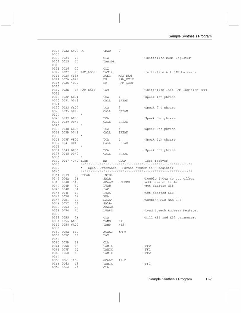
Sample Synthesis Program
D-7 Sample Synthesis Program
0306 0022 6900 GO TMAD 003070308 0024 2F CLA ;Initialize mode register0309 0025 1D TAMODE03100311 0026 20 CLX0312 0027 13 RAM_LOOP TAMIX ;Initialize All RAM to zeros0313 0028 61FF XGEC MAX_RAM0314 002A 402E BR RAM_EXIT0315 002C 4027 BR RAM_LOOP03160317 002E 16 RAM_EXIT TAM ;initialize last RAM location (FF)03180319 002F 6E01 TCA 1 ;Speak 1st phrase0320 0031 0049 CALL SPEAK03210322 0033 6E02 TCA 2 ;Speak 2nd phrase0323 0035 0049 CALL SPEAK0324 *0325 0037 6E03 TCA 3 ;Speak 3rd phrase0326 0039 0049 CALL SPEAK0327 *0328 003B 6E04 TCA 4 ;Speak 4th phrase0329 003D 0049 CALL SPEAK0330 *0331 003F 6E05 TCA 5 ;Speak 5th phrase0332 0041 0049 CALL SPEAK0333 *0334 0043 6E06 TCA 6 ;Speak 5th phrase0335 0045 0049 CALL SPEAK0336 *0337 0047 4047 glop BR GLOP ;loop forever0338 ***********************************************************0339 * Speak Utterance – Phrase number in A register0340 ***********************************************************0341 0049 3B SPEAK INTGR0342 004A 2E SALA ;Double index to get offset0343 004B 75A2 ACAAC SPEECH ;Add base of table0344 004D 6D LUAB ;get address MSB0345 004E 3A IAC0346 004F 6B LUAA ;Get address LSB0347 0050 12 XBA0348 0051 1B SALA4 ;Combine MSB and LSB0349 0052 1B SALA40350 0053 2C ABAAC0351 0054 6C LUAPS ;Load Speech Address Register03520353 0055 2F CLA ;Kill K11 and K12 parameters0354 0056 6A03 TAMD K110355 0058 6A02 TAMD K1203560357 005A 7FF0 ACAAC #FF00358 005C 18 TAX03590360 005D 2F CLA0361 005E 13 TAMIX ;FF00362 005F 13 TAMIX ;FF10363 0060 13 TAMIX ;FF203640365 0061 7162 ACAAC #1620366 0063 13 TAMIX ;FF30367 0064 2F CLA
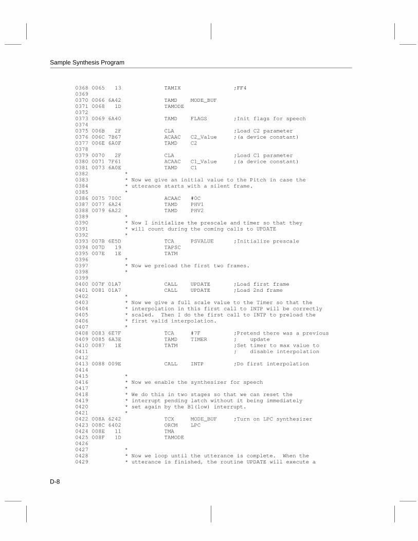
Sample Synthesis Program
D-8
0368 0065 13 TAMIX ;FF403690370 0066 6A42 TAMD MODE_BUF0371 0068 1D TAMODE03720373 0069 6A40 TAMD FLAGS ;Init flags for speech03740375 006B 2F CLA ;Load C2 parameter0376 006C 7B67 ACAAC C2_Value ;(a device constant)0377 006E 6A0F TAMD C203780379 0070 2F CLA ;Load C1 parameter0380 0071 7F61 ACAAC C1_Value ;(a device constant)0381 0073 6A0E TAMD C10382 *0383 * Now we give an initial value to the Pitch in case the0384 * utterance starts with a silent frame.0385 *0386 0075 700C ACAAC #0C0387 0077 6A24 TAMD PHV10388 0079 6A22 TAMD PHV20389 *0390 * Now I initialize the prescale and timer so that they0391 * will count during the coming calls to UPDATE0392 *0393 007B 6E5D TCA PSVALUE ;Initialize prescale0394 007D 19 TAPSC0395 007E 1E TATM0396 *0397 * Now we preload the first two frames.0398 *03990400 007F 01A7 CALL UPDATE ;Load first frame0401 0081 01A7 CALL UPDATE ;Load 2nd frame0402 *0403 * Now we give a full scale value to the Timer so that the0404 * interpolation in this first call to INTP will be correctly0405 * scaled. Then I do the first call to INTP to preload the0406 * first valid interpolation.0407 *0408 0083 6E7F TCA #7F ;Pretend there was a previous0409 0085 6A3E TAMD TIMER ; update0410 0087 1E TATM ;Set timer to max value to0411 ; disable interpolation04120413 0088 009E CALL INTP ;Do first interpolation04140415 *0416 * Now we enable the synthesizer for speech0417 *0418 * We do this in two stages so that we can reset the0419 * interrupt pending latch without it being immediately0420 * set again by the B1(low) interrupt.0421 *0422 008A 6242 TCX MODE_BUF ;Turn on LPC synthesizer0423 008C 6402 ORCM LPC0424 008E 11 TMA0425 008F 1D TAMODE04260427 *0428 * Now we loop until the utterance is complete. When the0429 * utterance is finished, the routine UPDATE will execute a
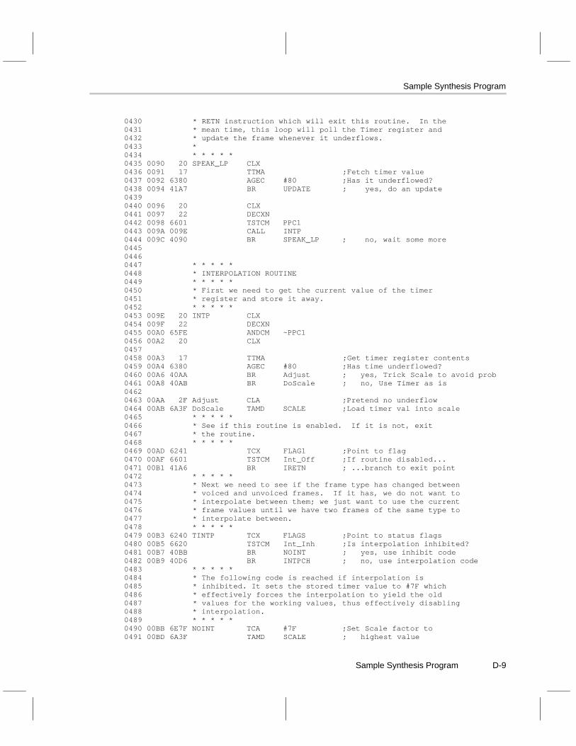
Sample Synthesis Program
D-9 Sample Synthesis Program
0430 * RETN instruction which will exit this routine. In the0431 * mean time, this loop will poll the Timer register and0432 * update the frame whenever it underflows.0433 *0434 * * * * *0435 0090 20 SPEAK_LP CLX0436 0091 17 TTMA ;Fetch timer value0437 0092 6380 AGEC #80 ;Has it underflowed?0438 0094 41A7 BR UPDATE ; yes, do an update04390440 0096 20 CLX0441 0097 22 DECXN0442 0098 6601 TSTCM PPC10443 009A 009E CALL INTP0444 009C 4090 BR SPEAK_LP ; no, wait some more044504460447 * * * * *0448 * INTERPOLATION ROUTINE0449 * * * * *0450 * First we need to get the current value of the timer0451 * register and store it away.0452 * * * * *0453 009E 20 INTP CLX0454 009F 22 DECXN0455 00A0 65FE ANDCM ~PPC10456 00A2 20 CLX04570458 00A3 17 TTMA ;Get timer register contents0459 00A4 6380 AGEC #80 ;Has time underflowed?0460 00A6 40AA BR Adjust ; yes, Trick Scale to avoid prob0461 00A8 40AB BR DoScale ; no, Use Timer as is04620463 00AA 2F Adjust CLA ;Pretend no underflow0464 00AB 6A3F DoScale TAMD SCALE ;Load timer val into scale0465 * * * * *0466 * See if this routine is enabled. If it is not, exit0467 * the routine.0468 * * * * *0469 00AD 6241 TCX FLAG1 ;Point to flag0470 00AF 6601 TSTCM Int_Off ;If routine disabled...0471 00B1 41A6 BR IRETN ; ...branch to exit point0472 * * * * *0473 * Next we need to see if the frame type has changed between0474 * voiced and unvoiced frames. If it has, we do not want to0475 * interpolate between them; we just want to use the current0476 * frame values until we have two frames of the same type to0477 * interpolate between.0478 * * * * *0479 00B3 6240 TINTP TCX FLAGS ;Point to status flags0480 00B5 6620 TSTCM Int_Inh ;Is interpolation inhibited?0481 00B7 40BB BR NOINT ; yes, use inhibit code0482 00B9 40D6 BR INTPCH ; no, use interpolation code0483 * * * * *0484 * The following code is reached if interpolation is0485 * inhibited. It sets the stored timer value to #7F which0486 * effectively forces the interpolation to yield the old0487 * values for the working values, thus effectively disabling0488 * interpolation.0489 * * * * *0490 00BB 6E7F NOINT TCA #7F ;Set Scale factor to0491 00BD 6A3F TAMD SCALE ; highest value
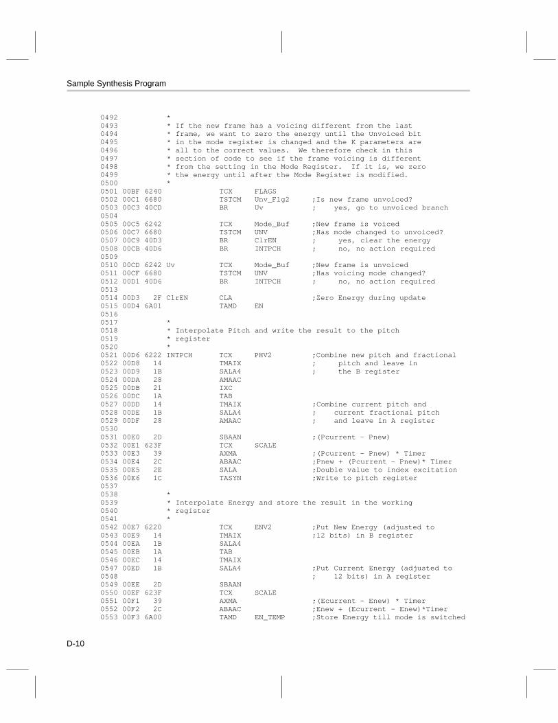
Sample Synthesis Program
D-10
0492 *0493 * If the new frame has a voicing different from the last0494 * frame, we want to zero the energy until the Unvoiced bit0495 * in the mode register is changed and the K parameters are0496 * all to the correct values. We therefore check in this0497 * section of code to see if the frame voicing is different0498 * from the setting in the Mode Register. If it is, we zero0499 * the energy until after the Mode Register is modified.0500 *0501 00BF 6240 TCX FLAGS0502 00C1 6680 TSTCM Unv_Flg2 ;Is new frame unvoiced?0503 00C3 40CD BR Uv ; yes, go to unvoiced branch05040505 00C5 6242 TCX Mode_Buf ;New frame is voiced0506 00C7 6680 TSTCM UNV ;Has mode changed to unvoiced?0507 00C9 40D3 BR ClrEN ; yes, clear the energy0508 00CB 40D6 BR INTPCH ; no, no action required05090510 00CD 6242 Uv TCX Mode_Buf ;New frame is unvoiced0511 00CF 6680 TSTCM UNV ;Has voicing mode changed?0512 00D1 40D6 BR INTPCH ; no, no action required05130514 00D3 2F ClrEN CLA ;Zero Energy during update0515 00D4 6A01 TAMD EN05160517 *0518 * Interpolate Pitch and write the result to the pitch0519 * register0520 *0521 00D6 6222 INTPCH TCX PHV2 ;Combine new pitch and fractional0522 00D8 14 TMAIX ; pitch and leave in0523 00D9 1B SALA4 ; the B register0524 00DA 28 AMAAC0525 00DB 21 IXC0526 00DC 1A TAB0527 00DD 14 TMAIX ;Combine current pitch and0528 00DE 1B SALA4 ; current fractional pitch0529 00DF 28 AMAAC ; and leave in A register05300531 00E0 2D SBAAN ;(Pcurrent – Pnew)0532 00E1 623F TCX SCALE0533 00E3 39 AXMA ;(Pcurrent – Pnew) * Timer0534 00E4 2C ABAAC ;Pnew + (Pcurrent – Pnew)* Timer0535 00E5 2E SALA ;Double value to index excitation0536 00E6 1C TASYN ;Write to pitch register05370538 *0539 * Interpolate Energy and store the result in the working0540 * register0541 *0542 00E7 6220 TCX ENV2 ;Put New Energy (adjusted to0543 00E9 14 TMAIX ;12 bits) in B register0544 00EA 1B SALA40545 00EB 1A TAB0546 00EC 14 TMAIX0547 00ED 1B SALA4 ;Put Current Energy (adjusted to0548 ; 12 bits) in A register0549 00EE 2D SBAAN0550 00EF 623F TCX SCALE0551 00F1 39 AXMA ;(Ecurrent – Enew) * Timer0552 00F2 2C ABAAC ;Enew + (Ecurrent – Enew)*Timer0553 00F3 6A00 TAMD EN_TEMP ;Store Energy till mode is switched
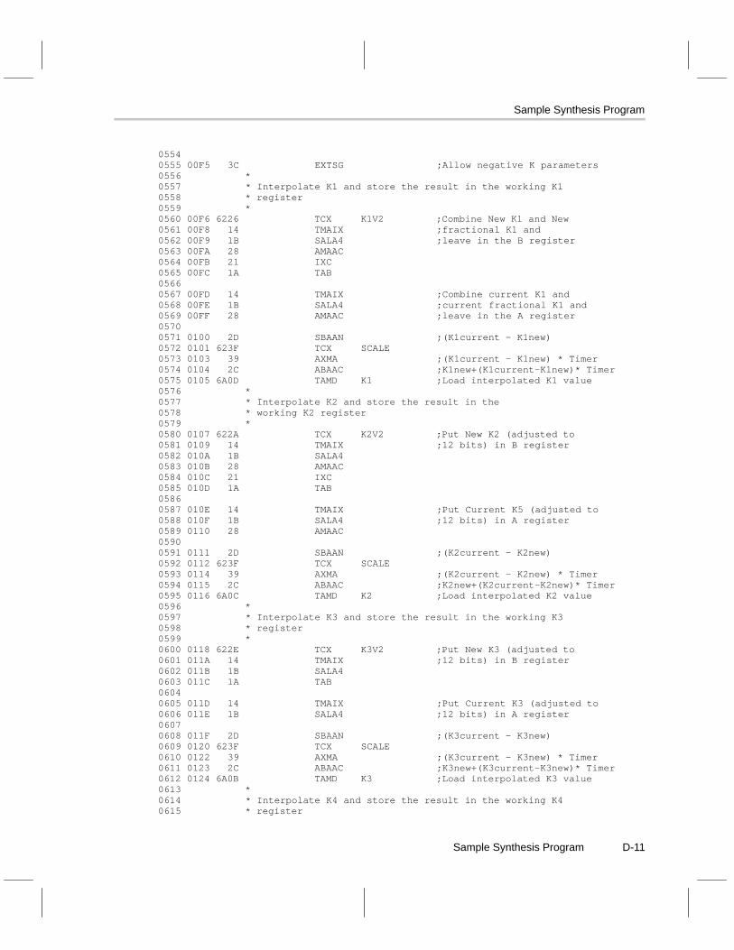
Sample Synthesis Program
D-11 Sample Synthesis Program
05540555 00F5 3C EXTSG ;Allow negative K parameters0556 *0557 * Interpolate K1 and store the result in the working K10558 * register0559 *0560 00F6 6226 TCX K1V2 ;Combine New K1 and New0561 00F8 14 TMAIX ;fractional K1 and0562 00F9 1B SALA4 ;leave in the B register0563 00FA 28 AMAAC0564 00FB 21 IXC0565 00FC 1A TAB05660567 00FD 14 TMAIX ;Combine current K1 and0568 00FE 1B SALA4 ;current fractional K1 and0569 00FF 28 AMAAC ;leave in the A register05700571 0100 2D SBAAN ;(K1current – K1new)0572 0101 623F TCX SCALE0573 0103 39 AXMA ;(K1current – K1new) * Timer0574 0104 2C ABAAC ;K1new+(K1current–K1new)* Timer0575 0105 6A0D TAMD K1 ;Load interpolated K1 value0576 *0577 * Interpolate K2 and store the result in the0578 * working K2 register0579 *0580 0107 622A TCX K2V2 ;Put New K2 (adjusted to0581 0109 14 TMAIX ;12 bits) in B register0582 010A 1B SALA40583 010B 28 AMAAC0584 010C 21 IXC0585 010D 1A TAB05860587 010E 14 TMAIX ;Put Current K5 (adjusted to0588 010F 1B SALA4 ;12 bits) in A register0589 0110 28 AMAAC05900591 0111 2D SBAAN ;(K2current – K2new)0592 0112 623F TCX SCALE0593 0114 39 AXMA ;(K2current – K2new) * Timer0594 0115 2C ABAAC ;K2new+(K2current–K2new)* Timer0595 0116 6A0C TAMD K2 ;Load interpolated K2 value0596 *0597 * Interpolate K3 and store the result in the working K30598 * register0599 *0600 0118 622E TCX K3V2 ;Put New K3 (adjusted to0601 011A 14 TMAIX ;12 bits) in B register0602 011B 1B SALA40603 011C 1A TAB06040605 011D 14 TMAIX ;Put Current K3 (adjusted to0606 011E 1B SALA4 ;12 bits) in A register06070608 011F 2D SBAAN ;(K3current – K3new)0609 0120 623F TCX SCALE0610 0122 39 AXMA ;(K3current – K3new) * Timer0611 0123 2C ABAAC ;K3new+(K3current–K3new)* Timer0612 0124 6A0B TAMD K3 ;Load interpolated K3 value0613 *0614 * Interpolate K4 and store the result in the working K40615 * register
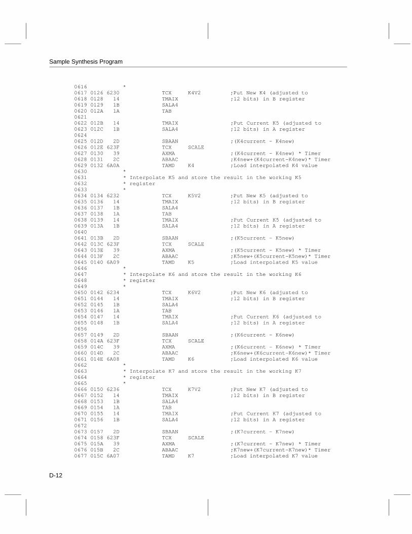
Sample Synthesis Program
D-12
0616 *0617 0126 6230 TCX K4V2 ;Put New K4 (adjusted to0618 0128 14 TMAIX ;12 bits) in B register0619 0129 1B SALA40620 012A 1A TAB06210622 012B 14 TMAIX ;Put Current K5 (adjusted to0623 012C 1B SALA4 ;12 bits) in A register06240625 012D 2D SBAAN ;(K4current – K4new)0626 012E 623F TCX SCALE0627 0130 39 AXMA ;(K4current – K4new) * Timer0628 0131 2C ABAAC ;K4new+(K4current–K4new)* Timer0629 0132 6A0A TAMD K4 ;Load interpolated K4 value0630 *0631 * Interpolate K5 and store the result in the working K50632 * register0633 *0634 0134 6232 TCX K5V2 ;Put New K5 (adjusted to0635 0136 14 TMAIX ;12 bits) in B register0636 0137 1B SALA40637 0138 1A TAB0638 0139 14 TMAIX ;Put Current K5 (adjusted to0639 013A 1B SALA4 ;12 bits) in A register06400641 013B 2D SBAAN ;(K5current – K5new)0642 013C 623F TCX SCALE0643 013E 39 AXMA ;(K5current – K5new) * Timer0644 013F 2C ABAAC ;K5new+(K5current–K5new)* Timer0645 0140 6A09 TAMD K5 ;Load interpolated K5 value0646 *0647 * Interpolate K6 and store the result in the working K60648 * register0649 *0650 0142 6234 TCX K6V2 ;Put New K6 (adjusted to0651 0144 14 TMAIX ;12 bits) in B register0652 0145 1B SALA40653 0146 1A TAB0654 0147 14 TMAIX ;Put Current K6 (adjusted to0655 0148 1B SALA4 ;12 bits) in A register06560657 0149 2D SBAAN ;(K6current – K6new)0658 014A 623F TCX SCALE0659 014C 39 AXMA ;(K6current – K6new) * Timer0660 014D 2C ABAAC ;K6new+(K6current–K6new)* Timer0661 014E 6A08 TAMD K6 ;Load interpolated K6 value0662 *0663 * Interpolate K7 and store the result in the working K70664 * register0665 *0666 0150 6236 TCX K7V2 ;Put New K7 (adjusted to0667 0152 14 TMAIX ;12 bits) in B register0668 0153 1B SALA40669 0154 1A TAB0670 0155 14 TMAIX ;Put Current K7 (adjusted to0671 0156 1B SALA4 ;12 bits) in A register06720673 0157 2D SBAAN ;(K7current – K7new)0674 0158 623F TCX SCALE0675 015A 39 AXMA ;(K7current – K7new) * Timer0676 015B 2C ABAAC ;K7new+(K7current–K7new)* Timer0677 015C 6A07 TAMD K7 ;Load interpolated K7 value
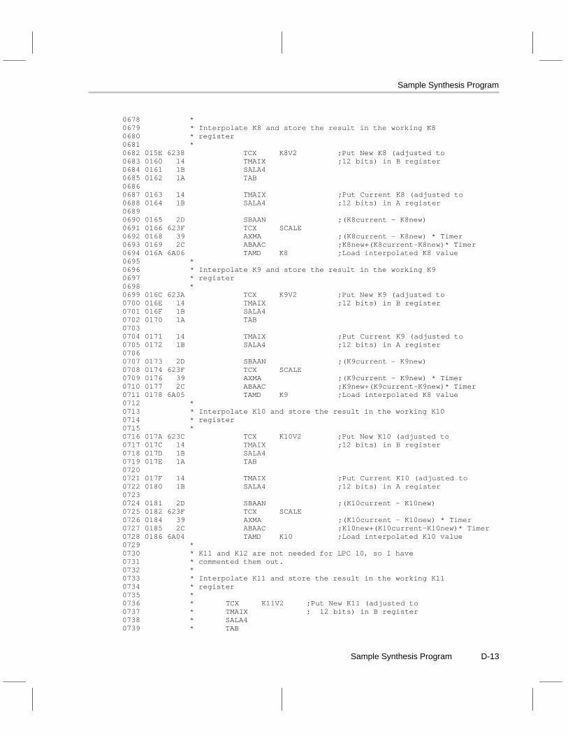
Sample Synthesis Program
D-13 Sample Synthesis Program
0678 *0679 * Interpolate K8 and store the result in the working K80680 * register0681 *0682 015E 6238 TCX K8V2 ;Put New K8 (adjusted to0683 0160 14 TMAIX ;12 bits) in B register0684 0161 1B SALA40685 0162 1A TAB06860687 0163 14 TMAIX ;Put Current K8 (adjusted to0688 0164 1B SALA4 ;12 bits) in A register06890690 0165 2D SBAAN ;(K8current – K8new)0691 0166 623F TCX SCALE0692 0168 39 AXMA ;(K8current – K8new) * Timer0693 0169 2C ABAAC ;K8new+(K8current–K8new)* Timer0694 016A 6A06 TAMD K8 ;Load interpolated K8 value0695 *0696 * Interpolate K9 and store the result in the working K90697 * register0698 *0699 016C 623A TCX K9V2 ;Put New K9 (adjusted to0700 016E 14 TMAIX ;12 bits) in B register0701 016F 1B SALA40702 0170 1A TAB07030704 0171 14 TMAIX ;Put Current K9 (adjusted to0705 0172 1B SALA4 ;12 bits) in A register07060707 0173 2D SBAAN ;(K9current – K9new)0708 0174 623F TCX SCALE0709 0176 39 AXMA ;(K9current – K9new) * Timer0710 0177 2C ABAAC ;K9new+(K9current–K9new)* Timer0711 0178 6A05 TAMD K9 ;Load interpolated K8 value0712 *0713 * Interpolate K10 and store the result in the working K100714 * register0715 *0716 017A 623C TCX K10V2 ;Put New K10 (adjusted to0717 017C 14 TMAIX ;12 bits) in B register0718 017D 1B SALA40719 017E 1A TAB07200721 017F 14 TMAIX ;Put Current K10 (adjusted to0722 0180 1B SALA4 ;12 bits) in A register07230724 0181 2D SBAAN ;(K10current – K10new)0725 0182 623F TCX SCALE0726 0184 39 AXMA ;(K10current – K10new) * Timer0727 0185 2C ABAAC ;K10new+(K10current–K10new)* Timer0728 0186 6A04 TAMD K10 ;Load interpolated K10 value0729 *0730 * K11 and K12 are not needed for LPC 10, so I have0731 * commented them out.0732 *0733 * Interpolate K11 and store the result in the working K110734 * register0735 *0736 * TCX K11V2 ;Put New K11 (adjusted to0737 * TMAIX ; 12 bits) in B register0738 * SALA40739 * TAB
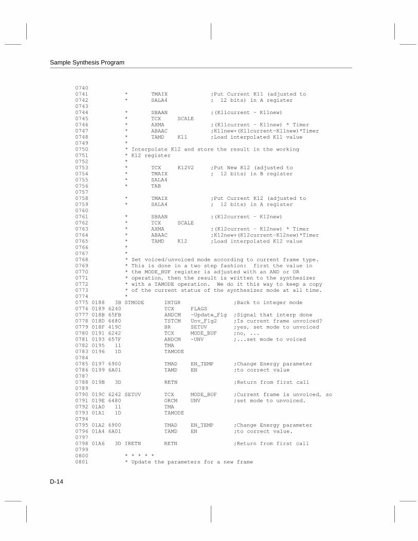
Sample Synthesis Program
D-14
07400741 * TMAIX ;Put Current K11 (adjusted to0742 * SALA4 ; 12 bits) in A register07430744 * SBAAN ;(K11current – K11new)0745 * TCX SCALE0746 * AXMA ;(K11current – K11new) * Timer0747 * ABAAC ;K11new+(K11current–K11new)*Timer0748 * TAMD K11 ;Load interpolated K11 value0749 *0750 * Interpolate K12 and store the result in the working0751 * K12 register0752 *0753 * TCX K12V2 ;Put New K12 (adjusted to0754 * TMAIX ; 12 bits) in B register0755 * SALA40756 * TAB07570758 * TMAIX ;Put Current K12 (adjusted to0759 * SALA4 ; 12 bits) in A register07600761 * SBAAN ;(K12current – K12new)0762 * TCX SCALE0763 * AXMA ;(K12current – K12new) * Timer0764 * ABAAC ;K12new+(K12current–K12new)*Timer0765 * TAMD K12 ;Load interpolated K12 value0766 *0767 *0768 * Set voiced/unvoiced mode according to current frame type.0769 * This is done in a two step fashion: first the value in0770 * the MODE_BUF register is adjusted with an AND or OR0771 * operation, then the result is written to the synthesizer0772 * with a TAMODE operation. We do it this way to keep a copy0773 * of the current status of the synthesizer mode at all time.0774 *0775 0188 3B STMODE INTGR ;Back to integer mode0776 0189 6240 TCX FLAGS0777 018B 65FB ANDCM ~Update_Flg ;Signal that interp done0778 018D 6680 TSTCM Unv_Flg2 ;Is current frame unvoiced?0779 018F 419C BR SETUV ;yes, set mode to unvoiced0780 0191 6242 TCX MODE_BUF ;no, ...0781 0193 657F ANDCM ~UNV ;...set mode to voiced0782 0195 11 TMA0783 0196 1D TAMODE07840785 0197 6900 TMAD EN_TEMP ;Change Energy parameter0786 0199 6A01 TAMD EN ;to correct value07870788 019B 3D RETN ;Return from first call07890790 019C 6242 SETUV TCX MODE_BUF ;Current frame is unvoiced, so0791 019E 6480 ORCM UNV ;set mode to unvoiced.0792 01A0 11 TMA0793 01A1 1D TAMODE07940795 01A2 6900 TMAD EN_TEMP ;Change Energy parameter0796 01A4 6A01 TAMD EN ;to correct value.07970798 01A6 3D IRETN RETN ;Return from first call07990800 * * * * *0801 * Update the parameters for a new frame

Sample Synthesis Program
D-15 Sample Synthesis Program
0802 * * * * *0803 * * * * *0804 * To prevent double updates, if the stored value of the0805 * timer register is zero, then we need to change it to #7F.0806 * If we do not do this, then the polling routine will0807 * discover an underflow and call Update a second time.0808 * * * * *0809 01A7 623E UPDATE TCX TIMER ;Get stored value0810 01A9 11 TMA ;of Timer into A08110812 01AA 6000 ANEC 0 ;Is it zero?0813 01AC 41B1 BR UPDT00 ;no, do nothing0814 01AE 6E7F TCA #7F ;yes, replace value0815 01B0 16 TAM0816 * * * * *0817 * First we need to test to see if a stop frame was0818 * encountered on the last pass through the routine. If the0819 * previous frame was a stop frame, we need to turn off the0820 * synthesizer and stop speaking.0821 * * * * *0822 01B1 6240 UPDT00 TCX FLAGS0823 01B3 6601 TSTCM STOPFLAG ;Was stop frame encountered0824 01B5 42C9 BR STOP ;yes, stop speaking0825 * * * * *0826 * Transfer the state of the previous frame to the Unvoiced0827 * flag (Current).0828 * * * * *0829 01B7 6610 TSTCM Unv_Flg1 ;Was previous frame unvoiced0830 01B9 41BF BR SUNVL ;yes, current frame=unvoiced0831 01BB 657F ANDCM ~Unv_Flg2 ;no, current frame=voiced0832 01BD 41C1 BR TSIL ;and continue08330834 01BF 6480 SUNVL ORCM Unv_Flg2 ;Set current frame unvoiced.0835 * * * * *0836 * Transfer the state of the previous frame to the0837 * Silence flag (Current).0838 * * * * *0839 01C1 6608 TSIL TSTCM Sil_Flg1 ;Was previous frame silent?0840 01C3 41C9 BR SSIL ;yes, current frame = silent0841 01C5 65BF ANDCM ~Sil_Flg2 ;no, current frame not silent0842 01C7 41CB BR ZROFLG ;and continue08430844 01C9 6440 SSIL ORCM Sil_Flg2 ;Set current frame silent0845 * * * * *0846 * Reset the Repeat Flag, new Silence Flag, new Unvoiced0847 * Flag, and Interpolation Inhibit flag so that new0848 * values can be loaded in this routine.0849 * * * * *0850 01CB 6240 ZROFLG TCX FLAGS0851 01CD 65C5 ANDCM #C50852 * * * * *0853 * Transfer the new frame parameters into the0854 * storage location used for the current frame parameters.0855 * * * * *0856 01CF 6220 TCX ENV2 ;Point to energy0857 01D1 14 TMAIX ;Transfer new frame En parameter0858 01D2 13 TAMIX ;to current frame location0859 *–––––PITCH–––––0860 01D3 14 TMAIX ;Transfer new frame pitch0861 01D4 6A24 TAMD PHV1 ;to current frame location08620863 01D6 14 TMAIX ;Transfer new fractional pitch
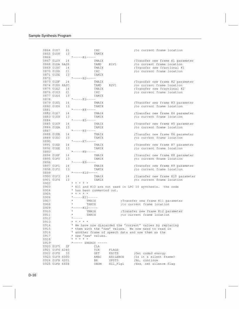
Sample Synthesis Program
D-16
0864 01D7 21 IXC ;to current frame location0865 01D8 13 TAMIX0866 *–––––K1–––––0867 01D9 14 TMAIX ;Transfer new frame K1 parameter0868 01DA 6A28 TAMD K1V1 ;to current frame location0869 01DC 14 TMAIX ;Transfer new fractional K10870 01DD 21 IXC ;to current frame location0871 01DE 13 TAMIX0872 *–––––K2–––––0873 01DF 14 TMAIX ;Transfer new frame K2 parameter0874 01E0 6A2C TAMD K2V1 ;to current frame location0875 01E2 14 TMAIX ;Transfer new fractional K20876 01E3 21 IXC ;to current frame location0877 01E4 13 TAMIX0878 *–––––K3–––––0879 01E5 14 TMAIX ;Transfer new frame K3 parameter0880 01E6 13 TAMIX ;to current frame location0881 *–––––K4–––––0882 01E7 14 TMAIX ;Transfer new frame K4 parameter0883 01E8 13 TAMIX ;to current frame location0884 *–––––K5–––––0885 01E9 14 TMAIX ;Transfer new frame K5 parameter0886 01EA 13 TAMIX ;to current frame location0887 *–––––K6–––––0888 01EB 14 TMAIX ;Transfer new frame K6 parameter0889 01EC 13 TAMIX ;to current frame location0890 *–––––K7–––––0891 01ED 14 TMAIX ;Transfer new frame K7 parameter0892 01EE 13 TAMIX ;to current frame location0893 *–––––K8–––––0894 01EF 14 TMAIX ;Transfer new frame K8 parameter0895 01F0 13 TAMIX ;to current frame location0896 *–––––K9–––––0897 01F1 14 TMAIX ;Transfer new frame K9 parameter0898 01F2 13 TAMIX ;to current frame location0899 *–––––K10–––––0900 01F3 14 TMAIX ;Transfer new frame K10 parameter0901 01F4 13 TAMIX ;to current frame location0902 * * * * *0903 * K11 and K12 are not used in LPC 10 synthesis. the code0904 * has been commented out.0905 * * * * *0906 *–––––K11–––––0907 * TMAIX ;Transfer new frame K11 parameter0908 * TAMIX ;to current frame location0909 *–––––K12–––––0910 * TMAIX ;Transfer new frame K12 parameter0911 * TAMIX ;to current frame location0912 *–––––0913 * * * * *0914 * We have now discarded the ”current” values by replacing0915 * them with the ”new” values. We now need to read in0916 * another frame of speech data and use them as the0917 * new ”new” values.0918 * * * * *0919 *––––– ENERGY –––––0920 01F5 2F CLA0921 01F6 6240 TCX FLAGS0922 01F8 33 GET EBITS ;Get coded energy0923 01F9 6000 ANEC ESILENCE ;Is it a silent frame?0924 01FB 4201 BR UPDT0 ;No, continue0925 01FD 6408 ORCM Sil_Flg1 ;Yes, set silence flag
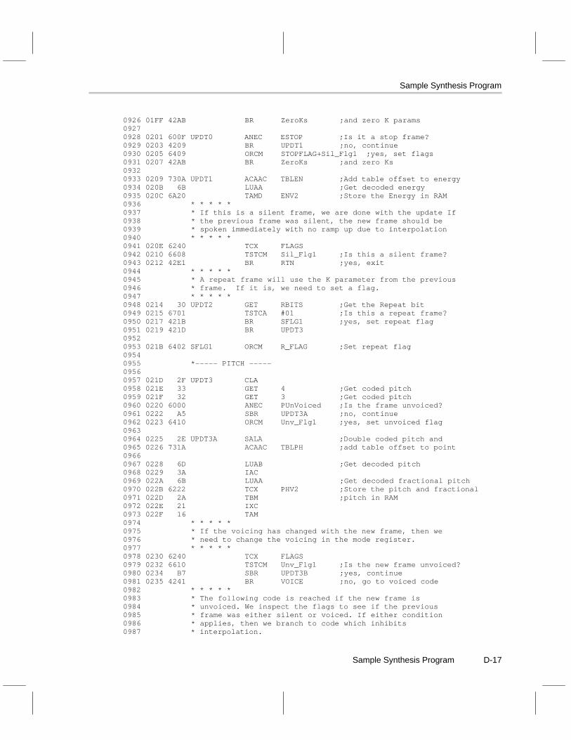
Sample Synthesis Program
D-17 Sample Synthesis Program
0926 01FF 42AB BR ZeroKs ;and zero K params09270928 0201 600F UPDT0 ANEC ESTOP ;Is it a stop frame?0929 0203 4209 BR UPDT1 ;no, continue0930 0205 6409 ORCM STOPFLAG+Sil_Flg1 ;yes, set flags0931 0207 42AB BR ZeroKs ;and zero Ks09320933 0209 730A UPDT1 ACAAC TBLEN ;Add table offset to energy0934 020B 6B LUAA ;Get decoded energy0935 020C 6A20 TAMD ENV2 ;Store the Energy in RAM0936 * * * * *0937 * If this is a silent frame, we are done with the update If0938 * the previous frame was silent, the new frame should be0939 * spoken immediately with no ramp up due to interpolation0940 * * * * *0941 020E 6240 TCX FLAGS0942 0210 6608 TSTCM Sil_Flg1 ;Is this a silent frame?0943 0212 42E1 BR RTN ;yes, exit0944 * * * * *0945 * A repeat frame will use the K parameter from the previous0946 * frame. If it is, we need to set a flag.0947 * * * * *0948 0214 30 UPDT2 GET RBITS ;Get the Repeat bit0949 0215 6701 TSTCA #01 ;Is this a repeat frame?0950 0217 421B BR SFLG1 ;yes, set repeat flag0951 0219 421D BR UPDT309520953 021B 6402 SFLG1 ORCM R_FLAG ;Set repeat flag09540955 *––––– PITCH –––––09560957 021D 2F UPDT3 CLA0958 021E 33 GET 4 ;Get coded pitch0959 021F 32 GET 3 ;Get coded pitch0960 0220 6000 ANEC PUnVoiced ;Is the frame unvoiced?0961 0222 A5 SBR UPDT3A ;no, continue0962 0223 6410 ORCM Unv_Flg1 ;yes, set unvoiced flag09630964 0225 2E UPDT3A SALA ;Double coded pitch and0965 0226 731A ACAAC TBLPH ;add table offset to point09660967 0228 6D LUAB ;Get decoded pitch0968 0229 3A IAC0969 022A 6B LUAA ;Get decoded fractional pitch0970 022B 6222 TCX PHV2 ;Store the pitch and fractional0971 022D 2A TBM ;pitch in RAM0972 022E 21 IXC0973 022F 16 TAM0974 * * * * *0975 * If the voicing has changed with the new frame, then we0976 * need to change the voicing in the mode register.0977 * * * * *0978 0230 6240 TCX FLAGS0979 0232 6610 TSTCM Unv_Flg1 ;Is the new frame unvoiced?0980 0234 B7 SBR UPDT3B ;yes, continue0981 0235 4241 BR VOICE ;no, go to voiced code0982 * * * * *0983 * The following code is reached if the new frame is0984 * unvoiced. We inspect the flags to see if the previous0985 * frame was either silent or voiced. If either condition0986 * applies, then we branch to code which inhibits0987 * interpolation.
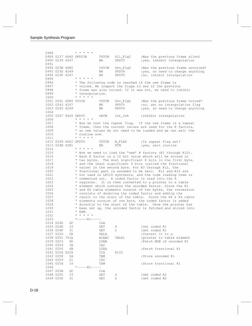
Sample Synthesis Program
D-18
0988 * * * * *0989 0237 6640 UPDT3B TSTCM Sil_Flg2 ;Was the previous frame silent0990 0239 4247 BR UPDT5 ;yes, inhibit interpolation09910992 023B 6680 TSTCM Unv_Flg2 ;Was the previous frame unvoiced?0993 023D 4249 BR UPDT4 ;yes, no need to change anything0994 023F 4247 BR UPDT5 ;no, inhibit interpolation0995 * * * * *0996 * The following code is reached if the new frame is0997 * voiced. We inspect the flags to see if the previous0998 * frame was also voiced. If it was not, we need to inhibit0999 * interpolation.1000 * * * * *1001 0241 6680 VOICE TSTCM Unv_Flg2 ;Was the previous frame voiced?1002 0243 4247 BR UPDT5 ;no, set no interpolation flag1003 0245 4249 BR UPDT4 ;yes, no need to change anything10041005 0247 6420 UPDT5 ORCM Int_Inh ;Inhibit interpolation1006 * * * * *1007 * Now we test the repeat flag. If the new frame is a repeat1008 * frame, then the current values are used for the K factors,1009 * so new values do not need to be loaded and we can exit the1010 * routine now.1011 * * * * *1012 0249 6602 UPDT4 TSTCM R_FLAG ;Is repeat flag set?1013 024B 42E1 BR RTN ;yes, exit routine1014 * * * * *1015 * Now we need to load the ”new” K factors (K1 through K10).1016 * Each K factor is a 12 bit value which will be stored in1017 * two bytes. The most significant 8 bits in the first byte,1018 * and the least significant 4 bits (called the fractional1019 * value) in the second byte. For K3 through K12, the1020 * fractional part is assumed to be zero. K11 and K12 are1021 * not used in LPC10 synthesis, and the code loading them is1022 * commented out. A coded factor is read into the A1023 * register. It is then converted to a pointer to a table1024 * element which contains the uncoded factor. Since the K11025 * and K2 table elements consist of two bytes, the conversion1026 * consists of doubling the coded factor and adding the1027 * result to the start of the table. Since the K4 & K4 table1028 * elements consist of one byte, the coded factor is added1029 * directly to the start of the table. Once the pointer has1030 * been set up, the uncoded factor is fetched and stored into1031 * RAM.1032 * * * * *1033 *–––––K1–––––1034 024D 2F CLA1035 024E 33 GET 4 ;Get coded K11036 024F 31 GET 2 ;Get coded K11037 0250 2E SALA ;Convert it to a1038 0251 741A ACAAC TBLK1 ;pointer to table element1039 0253 6D LUAB ;Fetch MSB of uncoded K11040 0254 3A IAC1041 0255 6B LUAA ;Fetch fractional K11042 0256 6226 TCX K1V21043 0258 2A TBM ;Store uncoded K11044 0259 21 IXC1045 025A 16 TAM ;Store fractional K11046 *–––––K2–––––1047 025B 2F CLA1048 025C 33 GET 4 ;Get coded K21049 025D 31 GET 2 ;Get coded K2
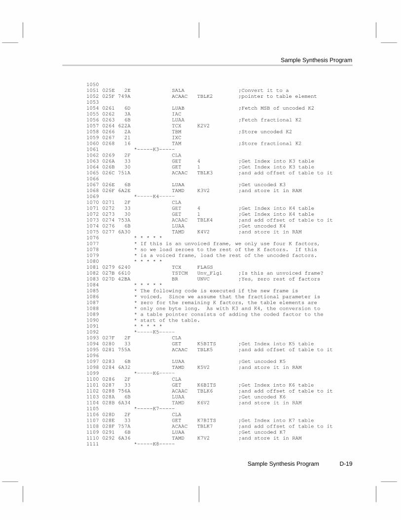
Sample Synthesis Program
D-19 Sample Synthesis Program
10501051 025E 2E SALA ;Convert it to a1052 025F 749A ACAAC TBLK2 ;pointer to table element10531054 0261 6D LUAB ;Fetch MSB of uncoded K21055 0262 3A IAC1056 0263 6B LUAA ;Fetch fractional K21057 0264 622A TCX K2V21058 0266 2A TBM ;Store uncoded K21059 0267 21 IXC1060 0268 16 TAM ;Store fractional K21061 *–––––K3–––––1062 0269 2F CLA1063 026A 33 GET 4 ;Get Index into K3 table1064 026B 30 GET 1 ;Get Index into K3 table1065 026C 751A ACAAC TBLK3 ;and add offset of table to it10661067 026E 6B LUAA ;Get uncoded K31068 026F 6A2E TAMD K3V2 ;and store it in RAM1069 *–––––K4–––––1070 0271 2F CLA1071 0272 33 GET 4 ;Get Index into K4 table1072 0273 30 GET 1 ;Get Index into K4 table1073 0274 753A ACAAC TBLK4 ;and add offset of table to it1074 0276 6B LUAA ;Get uncoded K41075 0277 6A30 TAMD K4V2 ;and store it in RAM1076 * * * * *1077 * If this is an unvoiced frame, we only use four K factors,1078 * so we load zeroes to the rest of the K factors. If this1079 * is a voiced frame, load the rest of the uncoded factors.1080 * * * * *1081 0279 6240 TCX FLAGS1082 027B 6610 TSTCM Unv_Flg1 ;Is this an unvoiced frame?1083 027D 42BA BR UNVC ;Yes, zero rest of factors1084 * * * * *1085 * The following code is executed if the new frame is1086 * voiced. Since we assume that the fractional parameter is1087 * zero for the remaining K factors, the table elements are1088 * only one byte long. As with K3 and K4, the conversion to1089 * a table pointer consists of adding the coded factor to the1090 * start of the table.1091 * * * * *1092 *–––––K5–––––1093 027F 2F CLA1094 0280 33 GET K5BITS ;Get Index into K5 table1095 0281 755A ACAAC TBLK5 ;and add offset of table to it10961097 0283 6B LUAA ;Get uncoded K51098 0284 6A32 TAMD K5V2 ;and store it in RAM1099 *–––––K6–––––1100 0286 2F CLA1101 0287 33 GET K6BITS ;Get Index into K6 table1102 0288 756A ACAAC TBLK6 ;and add offset of table to it1103 028A 6B LUAA ;Get uncoded K61104 028B 6A34 TAMD K6V2 ;and store it in RAM1105 *–––––K7–––––1106 028D 2F CLA1107 028E 33 GET K7BITS ;Get Index into K7 table1108 028F 757A ACAAC TBLK7 ;and add offset of table to it1109 0291 6B LUAA ;Get uncoded K71110 0292 6A36 TAMD K7V2 ;and store it in RAM1111 *–––––K8–––––
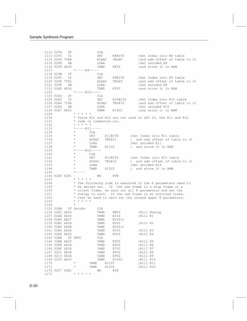
Sample Synthesis Program
D-20
1112 0294 2F CLA1113 0295 32 GET K8BITS ;Get Index into K8 table1114 0296 758A ACAAC TBLK8 ;and add offset of table to it1115 0298 6B LUAA ;Get uncoded K81116 0299 6A38 TAMD K8V2 ;and store it in RAM1117 *–––––K9–––––1118 029B 2F CLA1119 029C 32 GET K9BITS ;Get Index into K9 table1120 029D 7592 ACAAC TBLK9 ;and add offset of table to it1121 029F 6B LUAA ;Get uncoded K91122 02A0 6A3A TAMD K9V2 ;and store it in RAM1123 *–––––K10–––––1124 02A2 2F CLA1125 02A3 32 GET K10BITS ;Get Index into K10 table1126 02A4 759A ACAAC TBLK10 ;and add offset of table to it1127 02A6 6B LUAA ;Get uncoded K101128 02A7 6A3C TAMD K10V2 ;and store it in RAM1129 * * * * *1130 * Since K11 and K12 are not used in LPC 10, the K11 and K121131 * code is commented out.1132 * * * * *1133 *–––––K11–––––1134 * CLA1135 * GET K11BITS ;Get Index into K11 table1136 * ACAAC TBLK11 ; and add offset of table to it1137 * LUAA ;Get uncoded K111138 * TAMD K11V2 ; and store it in RAM1139 *–––––K12–––––1140 * CLA1141 * GET K12BITS ;Get Index into K12 table1142 * ACAAC TBLK12 ; and add offset of table to it1143 * LUAA ;Get uncoded K121144 * TAMD K12V2 ; and store it in RAM1145 *–––––1146 02A9 42E1 BR RTN1147 * * * * *1148 * The following code is executed if the K parameters need to1149 * be zeroed out. If the new frame is a stop frame or a1150 * silent frame, we zero out all K parameters and set the1151 * energy to zero. If the new frame is an unvoiced frame,1152 * then we need to zero out the unused upper K parameters.1153 * * * * *1154 *1155 02AB 2F ZeroKs CLA1156 02AC 6A20 TAMD ENV2 ;Kill Energy1157 02AE 6A26 TAMD K1V2 ;Kill K11158 02B0 6A27 TAMD K1V2+11159 02B2 6A2A TAMD K2V2 ;Kill K21160 02B4 6A2B TAMD K2V2+11161 02B6 6A2E TAMD K3V2 ;Kill K31162 02B8 6A30 TAMD K4V2 ;Kill K41163 02BA 2F UNVC CLA1164 02BB 6A32 TAMD K5V2 ;Kill K51165 02BD 6A34 TAMD K6V2 ;Kill K61166 02BF 6A36 TAMD K7V2 ;Kill K71167 02C1 6A38 TAMD K8V2 ;Kill K81168 02C3 6A3A TAMD K9V2 ;Kill K91169 02C5 6A3C TAMD K10V2 ;Kill K101170 * TAMD K11V2 ;Kill K111171 * TAMD K12V2 ;Kill K121172 02C7 42E1 BR RTN1173 * * * * *
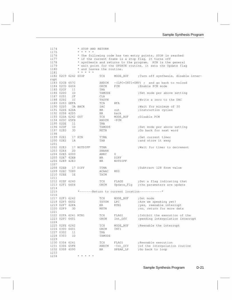
Sample Synthesis Program
D-21 Sample Synthesis Program
1174 * STOP AND RETURN1175 * * * * *1176 * The following code has two entry points. STOP is reached1177 * if the current frame is a stop flag, it turns off1178 * synthesis and returns to the program. RTN is the general1179 * exit point for the UPDATE routine, it sets the Update flag1180 * and leaves the routine.1181 * * * * *1182 02C9 6242 STOP TCX MODE_BUF ;Turn off synthesis, disable inter-rupt1183 02CB 657C ANDCM ~(LPC+INT1+UNV) ; and go back to voiced1184 02CD 6404 ORCM PCM ;Enable PCM mode1185 02CF 11 TMA1186 02D0 1D TAMODE ;Set mode per above setting1187 02D1 2F CLA1188 02D2 1C TASYN ;Write a zero to the DAC1189 02D3 6EFA TCA #FA1190 02D5 3A BACK IAC ;Wait for minimum of 301191 02D6 42DA BR out ;instruction cycles1192 02D8 42D5 BR back1193 02DA 6242 OUT TCX MODE_BUF ;Disable PCM1194 02DC 65FB ANDCM ~PCM1195 02DE 11 TMA1196 02DF 1D TAMODE ;Set mode per above setting1197 02E0 3D RETN ;Go back for next word11981199 02E1 17 RTN TTMA ;Get current timer1200 02E2 1A TAB ;and store it away12011202 02E3 17 NOTDIFF TTMA ;Wait for timer to decrement1203 02E4 2D SBAAN1204 02E5 6000 ANEC 01205 02E7 42EB BR DIFF1206 02E9 42E3 BR NOTDIFF12071208 02EB 17 DIFF TTMA ;Subtract 128 from value1209 02EC 7080 ACAAC #801210 02EE 1E TATM12111212 02EF 6240 TCX FLAGS ;Set a flag indicating that1213 02F1 6404 ORCM Update_Flg ;the parameters are update12141215 *–––––––Return to current location––––––––––––*12161217 02F3 6242 TCX MODE_BUF ;Get mode1218 02F5 6602 TSTCM LPC ;Are we speaking yet?1219 02F7 42FA BR RTN1 ;yes, reenable interrupt1220 02F9 3D RETN ;no, return for more data12211222 02FA 6241 RTN1 TCX FLAG1 ;Inhibit the execution of the1223 02FC 6401 ORCM Int_Off ;pending interpolation interrupt12241225 02FE 6242 TCX MODE_BUF ;Reenable the interrupt1226 0300 6401 ORCM INT11227 0302 11 TMA1228 0303 1D TAMODE12291230 0304 6241 TCX FLAG1 ;Reenable execution1231 0306 65FE ANDCM ~Int_Off ;of the interpolation routine1232 0308 4090 BR SPEAK_LP ;Go back to loop12331234 * * * * *
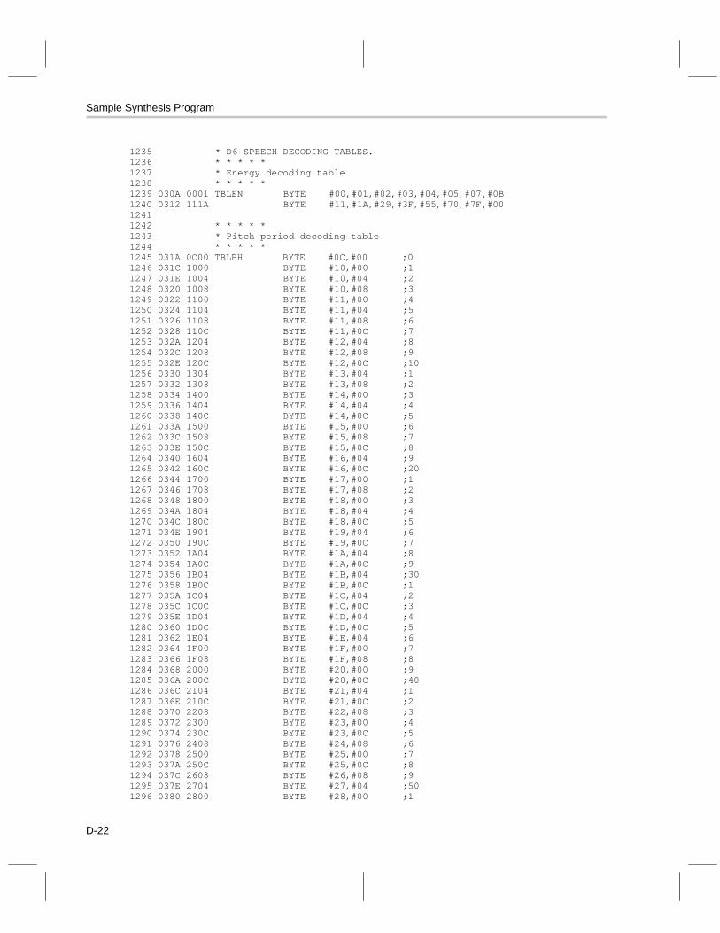
Sample Synthesis Program
D-22
1235 * D6 SPEECH DECODING TABLES.1236 * * * * *1237 * Energy decoding table1238 * * * * *1239 030A 0001 TBLEN BYTE #00,#01,#02,#03,#04,#05,#07,#0B1240 0312 111A BYTE #11,#1A,#29,#3F,#55,#70,#7F,#0012411242 * * * * *1243 * Pitch period decoding table1244 * * * * *1245 031A 0C00 TBLPH BYTE #0C,#00 ;01246 031C 1000 BYTE #10,#00 ;11247 031E 1004 BYTE #10,#04 ;21248 0320 1008 BYTE #10,#08 ;31249 0322 1100 BYTE #11,#00 ;41250 0324 1104 BYTE #11,#04 ;51251 0326 1108 BYTE #11,#08 ;61252 0328 110C BYTE #11,#0C ;71253 032A 1204 BYTE #12,#04 ;81254 032C 1208 BYTE #12,#08 ;91255 032E 120C BYTE #12,#0C ;101256 0330 1304 BYTE #13,#04 ;11257 0332 1308 BYTE #13,#08 ;21258 0334 1400 BYTE #14,#00 ;31259 0336 1404 BYTE #14,#04 ;41260 0338 140C BYTE #14,#0C ;51261 033A 1500 BYTE #15,#00 ;61262 033C 1508 BYTE #15,#08 ;71263 033E 150C BYTE #15,#0C ;81264 0340 1604 BYTE #16,#04 ;91265 0342 160C BYTE #16,#0C ;201266 0344 1700 BYTE #17,#00 ;11267 0346 1708 BYTE #17,#08 ;21268 0348 1800 BYTE #18,#00 ;31269 034A 1804 BYTE #18,#04 ;41270 034C 180C BYTE #18,#0C ;51271 034E 1904 BYTE #19,#04 ;61272 0350 190C BYTE #19,#0C ;71273 0352 1A04 BYTE #1A,#04 ;81274 0354 1A0C BYTE #1A,#0C ;91275 0356 1B04 BYTE #1B,#04 ;301276 0358 1B0C BYTE #1B,#0C ;11277 035A 1C04 BYTE #1C,#04 ;21278 035C 1C0C BYTE #1C,#0C ;31279 035E 1D04 BYTE #1D,#04 ;41280 0360 1D0C BYTE #1D,#0C ;51281 0362 1E04 BYTE #1E,#04 ;61282 0364 1F00 BYTE #1F,#00 ;71283 0366 1F08 BYTE #1F,#08 ;81284 0368 2000 BYTE #20,#00 ;91285 036A 200C BYTE #20,#0C ;401286 036C 2104 BYTE #21,#04 ;11287 036E 210C BYTE #21,#0C ;21288 0370 2208 BYTE #22,#08 ;31289 0372 2300 BYTE #23,#00 ;41290 0374 230C BYTE #23,#0C ;51291 0376 2408 BYTE #24,#08 ;61292 0378 2500 BYTE #25,#00 ;71293 037A 250C BYTE #25,#0C ;81294 037C 2608 BYTE #26,#08 ;91295 037E 2704 BYTE #27,#04 ;501296 0380 2800 BYTE #28,#00 ;1
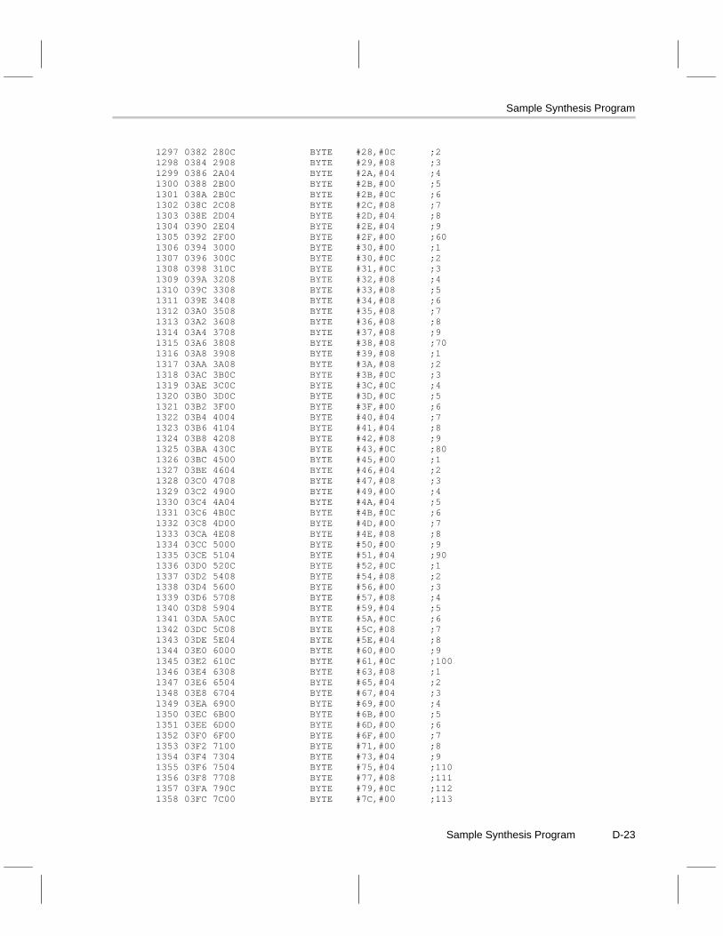
Sample Synthesis Program
D-23 Sample Synthesis Program
1297 0382 280C BYTE #28,#0C ;21298 0384 2908 BYTE #29,#08 ;31299 0386 2A04 BYTE #2A,#04 ;41300 0388 2B00 BYTE #2B,#00 ;51301 038A 2B0C BYTE #2B,#0C ;61302 038C 2C08 BYTE #2C,#08 ;71303 038E 2D04 BYTE #2D,#04 ;81304 0390 2E04 BYTE #2E,#04 ;91305 0392 2F00 BYTE #2F,#00 ;601306 0394 3000 BYTE #30,#00 ;11307 0396 300C BYTE #30,#0C ;21308 0398 310C BYTE #31,#0C ;31309 039A 3208 BYTE #32,#08 ;41310 039C 3308 BYTE #33,#08 ;51311 039E 3408 BYTE #34,#08 ;61312 03A0 3508 BYTE #35,#08 ;71313 03A2 3608 BYTE #36,#08 ;81314 03A4 3708 BYTE #37,#08 ;91315 03A6 3808 BYTE #38,#08 ;701316 03A8 3908 BYTE #39,#08 ;11317 03AA 3A08 BYTE #3A,#08 ;21318 03AC 3B0C BYTE #3B,#0C ;31319 03AE 3C0C BYTE #3C,#0C ;41320 03B0 3D0C BYTE #3D,#0C ;51321 03B2 3F00 BYTE #3F,#00 ;61322 03B4 4004 BYTE #40,#04 ;71323 03B6 4104 BYTE #41,#04 ;81324 03B8 4208 BYTE #42,#08 ;91325 03BA 430C BYTE #43,#0C ;801326 03BC 4500 BYTE #45,#00 ;11327 03BE 4604 BYTE #46,#04 ;21328 03C0 4708 BYTE #47,#08 ;31329 03C2 4900 BYTE #49,#00 ;41330 03C4 4A04 BYTE #4A,#04 ;51331 03C6 4B0C BYTE #4B,#0C ;61332 03C8 4D00 BYTE #4D,#00 ;71333 03CA 4E08 BYTE #4E,#08 ;81334 03CC 5000 BYTE #50,#00 ;91335 03CE 5104 BYTE #51,#04 ;901336 03D0 520C BYTE #52,#0C ;11337 03D2 5408 BYTE #54,#08 ;21338 03D4 5600 BYTE #56,#00 ;31339 03D6 5708 BYTE #57,#08 ;41340 03D8 5904 BYTE #59,#04 ;51341 03DA 5A0C BYTE #5A,#0C ;61342 03DC 5C08 BYTE #5C,#08 ;71343 03DE 5E04 BYTE #5E,#04 ;81344 03E0 6000 BYTE #60,#00 ;91345 03E2 610C BYTE #61,#0C ;1001346 03E4 6308 BYTE #63,#08 ;11347 03E6 6504 BYTE #65,#04 ;21348 03E8 6704 BYTE #67,#04 ;31349 03EA 6900 BYTE #69,#00 ;41350 03EC 6B00 BYTE #6B,#00 ;51351 03EE 6D00 BYTE #6D,#00 ;61352 03F0 6F00 BYTE #6F,#00 ;71353 03F2 7100 BYTE #71,#00 ;81354 03F4 7304 BYTE #73,#04 ;91355 03F6 7504 BYTE #75,#04 ;1101356 03F8 7708 BYTE #77,#08 ;1111357 03FA 790C BYTE #79,#0C ;1121358 03FC 7C00 BYTE #7C,#00 ;113
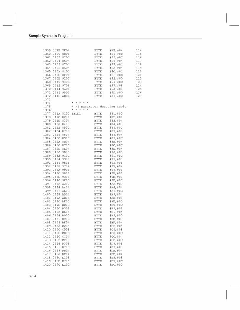
Sample Synthesis Program
D-24
1359 03FE 7E04 BYTE #7E,#04 ;1141360 0400 8008 BYTE #80,#08 ;1151361 0402 820C BYTE #82,#0C ;1161362 0404 8504 BYTE #85,#04 ;1171363 0406 870C BYTE #87,#0C ;1181364 0408 8A04 BYTE #8A,#04 ;1191365 040A 8C0C BYTE #8C,#0C ;1201366 040C 8F08 BYTE #8F,#08 ;1211367 040E 9200 BYTE #92,#00 ;1221368 0410 940C BYTE #94,#0C ;1231369 0412 9708 BYTE #97,#08 ;1241370 0414 9A04 BYTE #9A,#04 ;1251371 0416 9D00 BYTE #9D,#00 ;1261372 0418 A000 BYTE #A0,#00 ;12713731374 * * * * *1375 * K1 parameter decoding table1376 * * * * *1377 041A 8100 TBLK1 BYTE #81,#001378 041C 8204 BYTE #82,#041379 041E 8304 BYTE #83,#041380 0420 8408 BYTE #84,#081381 0422 850C BYTE #85,#0C1382 0424 8700 BYTE #87,#001383 0426 8804 BYTE #88,#041384 0428 890C BYTE #89,#0C1385 042A 8B04 BYTE #8B,#041386 042C 8C0C BYTE #8C,#0C1387 042E 8E04 BYTE #8E,#041388 0430 9000 BYTE #90,#001389 0432 910C BYTE #91,#0C1390 0434 9308 BYTE #93,#081391 0436 9508 BYTE #95,#081392 0438 9704 BYTE #97,#041393 043A 9908 BYTE #99,#081394 043C 9B08 BYTE #9B,#081395 043E 9D08 BYTE #9D,#081396 0440 9F0C BYTE #9F,#0C1397 0442 A200 BYTE #A2,#001398 0444 A404 BYTE #A4,#041399 0446 A60C BYTE #A6,#0C1400 0448 A904 BYTE #A9,#041401 044A AB08 BYTE #AB,#081402 044C AE00 BYTE #AE,#001403 044E B00C BYTE #B0,#0C1404 0450 B308 BYTE #B3,#081405 0452 B604 BYTE #B6,#041406 0454 B900 BYTE #B9,#001407 0456 BC00 BYTE #BC,#001408 0458 BF04 BYTE #BF,#041409 045A C204 BYTE #C2,#041410 045C C508 BYTE #C5,#081411 045E C80C BYTE #C8,#0C1412 0460 CC04 BYTE #CC,#041413 0462 CF0C BYTE #CF,#0C1414 0464 D308 BYTE #D3,#081415 0466 D708 BYTE #D7,#081416 0468 DB04 BYTE #DB,#041417 046A DF04 BYTE #DF,#041418 046C E308 BYTE #E3,#081419 046E E70C BYTE #E7,#0C1420 0470 EC00 BYTE #EC,#00
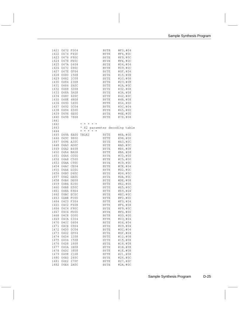
Sample Synthesis Program
D-25 Sample Synthesis Program
1421 0472 F004 BYTE #F0,#041422 0474 F40C BYTE #F4,#0C1423 0476 F90C BYTE #F9,#0C1424 0478 FE0C BYTE #FE,#0C1425 047A 0404 BYTE #04,#041426 047C 090C BYTE #09,#0C1427 047E 0F04 BYTE #0F,#041428 0480 1508 BYTE #15,#081429 0482 1C08 BYTE #1C,#081430 0484 2308 BYTE #23,#081431 0486 2A0C BYTE #2A,#0C1432 0488 3208 BYTE #32,#081433 048A 3A08 BYTE #3A,#081434 048C 420C BYTE #42,#0C1435 048E 4B08 BYTE #4B,#081436 0490 5400 BYTE #54,#001437 0492 5C04 BYTE #5C,#041438 0494 6500 BYTE #65,#001439 0496 6E00 BYTE #6E,#001440 0498 7808 BYTE #78,#0814411442 * * * * *1443 * K2 parameter decoding table1444 * * * * *1445 049A 8A00 TBLK2 BYTE #8A,#001446 049C 9800 BYTE #98,#001447 049E A30C BYTE #A3,#0C1448 04A0 AD0C BYTE #AD,#0C1449 04A2 B408 BYTE #B4,#081450 04A4 BA08 BYTE #BA,#081451 04A6 C000 BYTE #C0,#001452 04A8 C500 BYTE #C5,#001453 04AA C90C BYTE #C9,#0C1454 04AC CE04 BYTE #CE,#041455 04AE D20C BYTE #D2,#0C1456 04B0 D60C BYTE #D6,#0C1457 04B2 DA0C BYTE #DA,#0C1458 04B4 DE08 BYTE #DE,#081459 04B6 E200 BYTE #E2,#001460 04B8 E50C BYTE #E5,#0C1461 04BA E904 BYTE #E9,#041462 04BC EC0C BYTE #EC,#0C1463 04BE F000 BYTE #F0,#001464 04C0 F304 BYTE #F3,#041465 04C2 F608 BYTE #F6,#081466 04C4 F90C BYTE #F9,#0C1467 04C6 FD00 BYTE #FD,#001468 04C8 0000 BYTE #00,#001469 04CA 0304 BYTE #03,#041470 04CC 0604 BYTE #06,#041471 04CE 0904 BYTE #09,#041472 04D0 0C04 BYTE #0C,#041473 04D2 0F04 BYTE #0F,#041474 04D4 1208 BYTE #12,#081475 04D6 1508 BYTE #15,#081476 04D8 1808 BYTE #18,#081477 04DA 1B08 BYTE #1B,#081478 04DC 1E08 BYTE #1E,#081479 04DE 2108 BYTE #21,#081480 04E0 240C BYTE #24,#0C1481 04E2 270C BYTE #27,#0C1482 04E4 2A0C BYTE #2A,#0C
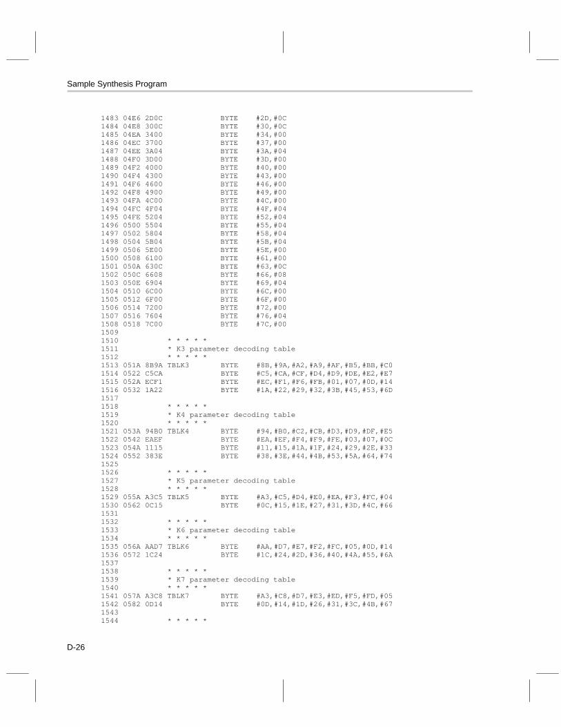
Sample Synthesis Program
D-26
1483 04E6 2D0C BYTE #2D,#0C1484 04E8 300C BYTE #30,#0C1485 04EA 3400 BYTE #34,#001486 04EC 3700 BYTE #37,#001487 04EE 3A04 BYTE #3A,#041488 04F0 3D00 BYTE #3D,#001489 04F2 4000 BYTE #40,#001490 04F4 4300 BYTE #43,#001491 04F6 4600 BYTE #46,#001492 04F8 4900 BYTE #49,#001493 04FA 4C00 BYTE #4C,#001494 04FC 4F04 BYTE #4F,#041495 04FE 5204 BYTE #52,#041496 0500 5504 BYTE #55,#041497 0502 5804 BYTE #58,#041498 0504 5B04 BYTE #5B,#041499 0506 5E00 BYTE #5E,#001500 0508 6100 BYTE #61,#001501 050A 630C BYTE #63,#0C1502 050C 6608 BYTE #66,#081503 050E 6904 BYTE #69,#041504 0510 6C00 BYTE #6C,#001505 0512 6F00 BYTE #6F,#001506 0514 7200 BYTE #72,#001507 0516 7604 BYTE #76,#041508 0518 7C00 BYTE #7C,#0015091510 * * * * *1511 * K3 parameter decoding table1512 * * * * *1513 051A 8B9A TBLK3 BYTE #8B,#9A,#A2,#A9,#AF,#B5,#BB,#C01514 0522 C5CA BYTE #C5,#CA,#CF,#D4,#D9,#DE,#E2,#E71515 052A ECF1 BYTE #EC,#F1,#F6,#FB,#01,#07,#0D,#141516 0532 1A22 BYTE #1A,#22,#29,#32,#3B,#45,#53,#6D15171518 * * * * *1519 * K4 parameter decoding table1520 * * * * *1521 053A 94B0 TBLK4 BYTE #94,#B0,#C2,#CB,#D3,#D9,#DF,#E51522 0542 EAEF BYTE #EA,#EF,#F4,#F9,#FE,#03,#07,#0C1523 054A 1115 BYTE #11,#15,#1A,#1F,#24,#29,#2E,#331524 0552 383E BYTE #38,#3E,#44,#4B,#53,#5A,#64,#7415251526 * * * * *1527 * K5 parameter decoding table1528 * * * * *1529 055A A3C5 TBLK5 BYTE #A3,#C5,#D4,#E0,#EA,#F3,#FC,#041530 0562 0C15 BYTE #0C,#15,#1E,#27,#31,#3D,#4C,#6615311532 * * * * *1533 * K6 parameter decoding table1534 * * * * *1535 056A AAD7 TBLK6 BYTE #AA,#D7,#E7,#F2,#FC,#05,#0D,#141536 0572 1C24 BYTE #1C,#24,#2D,#36,#40,#4A,#55,#6A15371538 * * * * *1539 * K7 parameter decoding table1540 * * * * *1541 057A A3C8 TBLK7 BYTE #A3,#C8,#D7,#E3,#ED,#F5,#FD,#051542 0582 0D14 BYTE #0D,#14,#1D,#26,#31,#3C,#4B,#6715431544 * * * * *
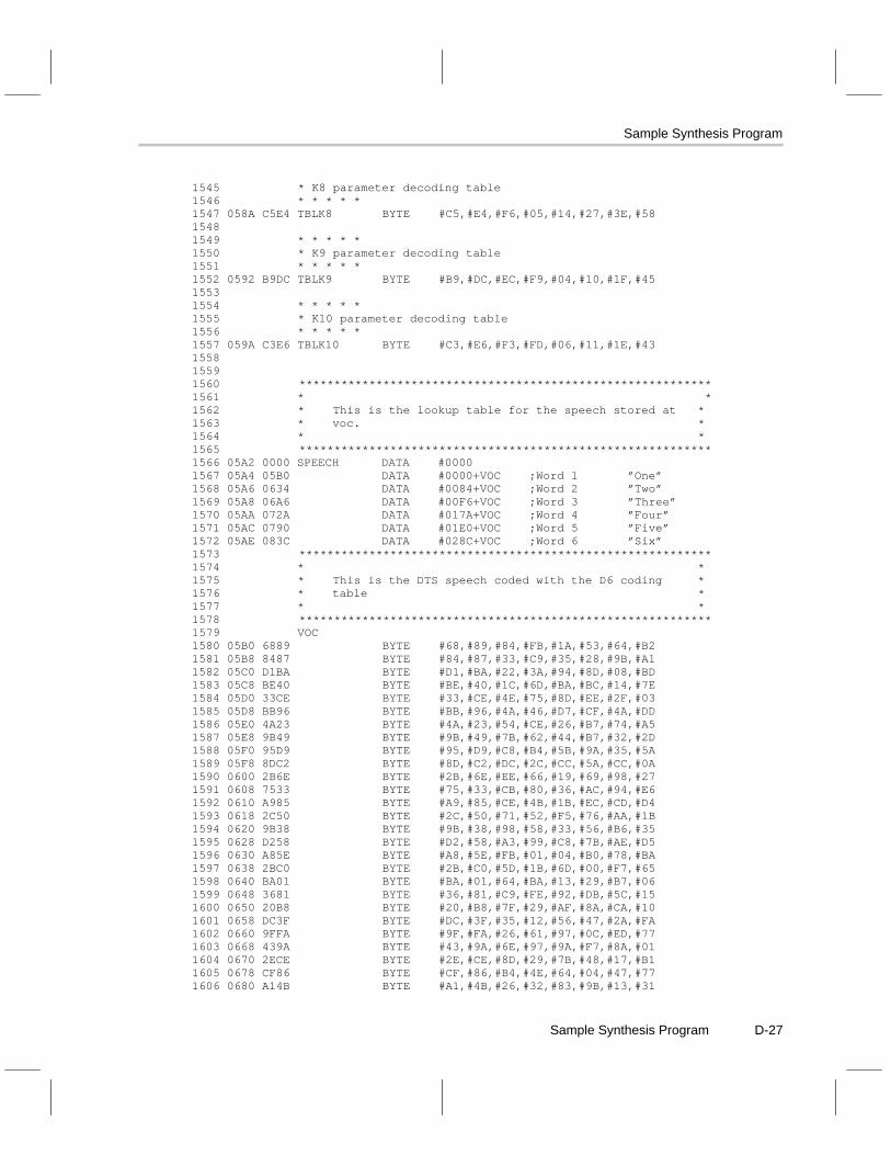
Sample Synthesis Program
D-27 Sample Synthesis Program
1545 * K8 parameter decoding table1546 * * * * *1547 058A C5E4 TBLK8 BYTE #C5,#E4,#F6,#05,#14,#27,#3E,#5815481549 * * * * *1550 * K9 parameter decoding table1551 * * * * *1552 0592 B9DC TBLK9 BYTE #B9,#DC,#EC,#F9,#04,#10,#1F,#4515531554 * * * * *1555 * K10 parameter decoding table1556 * * * * *1557 059A C3E6 TBLK10 BYTE #C3,#E6,#F3,#FD,#06,#11,#1E,#43155815591560 ***********************************************************1561 * *1562 * This is the lookup table for the speech stored at *1563 * voc. *1564 * *1565 ***********************************************************1566 05A2 0000 SPEECH DATA #00001567 05A4 05B0 DATA #0000+VOC ;Word 1 ”One”1568 05A6 0634 DATA #0084+VOC ;Word 2 ”Two”1569 05A8 06A6 DATA #00F6+VOC ;Word 3 ”Three”1570 05AA 072A DATA #017A+VOC ;Word 4 ”Four”1571 05AC 0790 DATA #01E0+VOC ;Word 5 ”Five”1572 05AE 083C DATA #028C+VOC ;Word 6 ”Six”1573 ***********************************************************1574 * *1575 * This is the DTS speech coded with the D6 coding *1576 * table *1577 * *1578 ***********************************************************1579 VOC1580 05B0 6889 BYTE #68,#89,#84,#FB,#1A,#53,#64,#B21581 05B8 8487 BYTE #84,#87,#33,#C9,#35,#28,#9B,#A11582 05C0 D1BA BYTE #D1,#BA,#22,#3A,#94,#8D,#08,#BD1583 05C8 BE40 BYTE #BE,#40,#1C,#6D,#BA,#BC,#14,#7E1584 05D0 33CE BYTE #33,#CE,#4E,#75,#8D,#EE,#2F,#031585 05D8 BB96 BYTE #BB,#96,#4A,#46,#D7,#CF,#4A,#DD1586 05E0 4A23 BYTE #4A,#23,#54,#CE,#26,#B7,#74,#A51587 05E8 9B49 BYTE #9B,#49,#7B,#62,#44,#B7,#32,#2D1588 05F0 95D9 BYTE #95,#D9,#C8,#B4,#5B,#9A,#35,#5A1589 05F8 8DC2 BYTE #8D,#C2,#DC,#2C,#CC,#5A,#CC,#0A1590 0600 2B6E BYTE #2B,#6E,#EE,#66,#19,#69,#98,#271591 0608 7533 BYTE #75,#33,#CB,#80,#36,#AC,#94,#E61592 0610 A985 BYTE #A9,#85,#CE,#4B,#1B,#EC,#CD,#D41593 0618 2C50 BYTE #2C,#50,#71,#52,#F5,#76,#AA,#1B1594 0620 9B38 BYTE #9B,#38,#98,#58,#33,#56,#B6,#351595 0628 D258 BYTE #D2,#58,#A3,#99,#C8,#7B,#AE,#D51596 0630 A85E BYTE #A8,#5E,#FB,#01,#04,#B0,#78,#BA1597 0638 2BC0 BYTE #2B,#C0,#5D,#1B,#6D,#00,#F7,#651598 0640 BA01 BYTE #BA,#01,#64,#BA,#13,#29,#B7,#061599 0648 3681 BYTE #36,#81,#C9,#FE,#92,#DB,#5C,#151600 0650 20B8 BYTE #20,#B8,#7F,#29,#AF,#8A,#CA,#101601 0658 DC3F BYTE #DC,#3F,#35,#12,#56,#47,#2A,#FA1602 0660 9FFA BYTE #9F,#FA,#26,#61,#97,#0C,#ED,#771603 0668 439A BYTE #43,#9A,#6E,#97,#9A,#F7,#8A,#011604 0670 2ECE BYTE #2E,#CE,#8D,#29,#7B,#48,#17,#B11605 0678 CF86 BYTE #CF,#86,#B4,#4E,#64,#04,#47,#771606 0680 A14B BYTE #A1,#4B,#26,#32,#83,#9B,#13,#31
Sample Synthesis Program
D-28
1607 0688 AD23 BYTE #AD,#23,#59,#E3,#DA,#5E,#90,#B21608 0690 85AC BYTE #85,#AC,#68,#65,#0D,#70,#E9,#4D1609 0698 3644 BYTE #36,#44,#38,#13,#87,#74,#12,#BB1610 06A0 8D52 BYTE #8D,#52,#59,#90,#E4,#3D,#08,#601611 06A8 CA86 BYTE #CA,#86,#13,#40,#66,#1A,#46,#001612 06B0 B9EC BYTE #B9,#EC,#8B,#00,#14,#59,#B7,#0A1613 06B8 905A BYTE #90,#5A,#35,#9A,#EC,#1E,#D9,#861614 06C0 A4EA BYTE #A4,#EA,#5C,#41,#69,#85,#B2,#A61615 06C8 EE21 BYTE #EE,#21,#AF,#CC,#24,#46,#63,#F71616 06D0 9453 BYTE #94,#53,#26,#E1,#65,#B1,#7B,#C91617 06D8 3BA5 BYTE #3B,#A5,#77,#B8,#92,#3E,#E5,#9B1618 06E0 B47B BYTE #B4,#7B,#18,#EE,#9F,#0A,#5B,#521619 06E8 02B4 BYTE #02,#B4,#EE,#4F,#8D,#23,#CF,#061620 06F0 2AB7 BYTE #2A,#B7,#A7,#FE,#96,#04,#0A,#DD1621 06F8 DFD2 BYTE #DF,#D2,#70,#B6,#24,#C6,#9D,#251622 0700 613C BYTE #61,#3C,#F0,#1C,#F3,#ED,#A4,#301623 0708 5974 BYTE #59,#74,#8E,#70,#E7,#96,#9B,#4C1624 0710 0A47 BYTE #0A,#47,#74,#3B,#D1,#CC,#07,#951625 0718 21BE BYTE #21,#BE,#19,#65,#A6,#B3,#27,#201626 0720 CE4C BYTE #CE,#4C,#62,#93,#58,#41,#B4,#771627 0728 0A3E BYTE #0A,#3E,#80,#00,#A6,#6A,#03,#011628 0730 54A6 BYTE #54,#A6,#4F,#0C,#10,#C6,#D1,#0B1629 0738 8097 BYTE #80,#97,#D4,#E0,#12,#2A,#D7,#371630 0740 8758 BYTE #87,#58,#09,#E9,#18,#B7,#3F,#0D1631 0748 BD87 BYTE #BD,#87,#74,#8A,#99,#9F,#86,#DE1632 0750 43D9 BYTE #43,#D9,#26,#EA,#37,#C5,#EC,#A11633 0758 A9B0 BYTE #A9,#B0,#F3,#91,#71,#FE,#30,#601634 0760 83B3 BYTE #83,#B3,#B1,#C4,#7F,#1A,#B3,#ED1635 0768 8ED4 BYTE #8E,#D4,#A2,#3F,#CC,#84,#AD,#4A1636 0770 1BE8 BYTE #1B,#E8,#1F,#D6,#EA,#38,#A4,#1C1637 0778 E60F BYTE #E6,#0F,#5B,#63,#49,#D4,#0F,#F31638 0780 B983 BYTE #B9,#83,#B1,#7B,#E2,#87,#7B,#DD1639 0788 D5BA BYTE #D5,#BA,#A8,#E8,#C5,#5D,#0F,#001640 0790 0890 BYTE #08,#90,#FB,#51,#23,#80,#AB,#191641 0798 4A00 BYTE #4A,#00,#B9,#97,#0D,#01,#34,#591642 07A0 490C BYTE #49,#0C,#D0,#A5,#29,#11,#80,#E51643 07A8 8658 BYTE #86,#58,#EA,#BE,#32,#36,#27,#F51644 07B0 69B5 BYTE #69,#B5,#4C,#18,#CB,#9B,#DA,#B51645 07B8 7AAA BYTE #7A,#AA,#EC,#61,#45,#6B,#4B,#331646 07C0 F06F BYTE #F0,#6F,#D1,#94,#25,#A5,#ED,#151647 07C8 3768 BYTE #37,#68,#EA,#9C,#D4,#75,#BA,#ED1648 07D0 346D BYTE #34,#6D,#4E,#19,#7B,#CD,#76,#9A1649 07D8 7ABB BYTE #7A,#BB,#CC,#A2,#F2,#18,#4D,#B91650 07E0 5996 BYTE #59,#96,#59,#71,#B4,#A4,#3C,#2A1651 07E8 CBBC BYTE #CB,#BC,#5A,#5C,#52,#67,#A6,#4D1652 07F0 3636 BYTE #36,#36,#AA,#61,#17,#D3,#2E,#6F1653 07F8 2293 BYTE #22,#93,#F4,#05,#61,#1F,#56,#521654 0800 69E7 BYTE #69,#E7,#41,#B3,#0F,#32,#E1,#AC1655 0808 E2B0 BYTE #E2,#B0,#D9,#EB,#95,#34,#5C,#7E1656 0810 52EC BYTE #52,#EC,#E5,#44,#1B,#4A,#79,#C11657 0818 F63A BYTE #F6,#3A,#6D,#1C,#9A,#76,#66,#BB1658 0820 5132 BYTE #51,#32,#16,#89,#94,#99,#DD,#961659 0828 8F69 BYTE #8F,#69,#C9,#6A,#D5,#6E,#F2,#521660 0830 2162 BYTE #21,#62,#6A,#62,#37,#24,#2D,#221661 0838 1197 BYTE #11,#97,#07,#00,#04,#F0,#2A,#081662 0840 13C0 BYTE #13,#C0,#BF,#F9,#44,#00,#FF,#EE1663 0848 9500 BYTE #95,#00,#7C,#A5,#D3,#02,#F0,#B51664 0850 DA94 BYTE #DA,#94,#62,#C6,#17,#8D,#D9,#B71665 0858 4BBE BYTE #4B,#BE,#97,#8B,#25,#CB,#D7,#A51666 0860 5AAA BYTE #5A,#AA,#4D,#72,#F7,#DB,#D4,#2F1667 0868 BD4C BYTE #BD,#4C,#75,#EA,#6B,#5A,#84,#151668 0870 D1DD BYTE #D1,#DD,#BD,#11,#00,#80,#01,#1C
Sample Synthesis Program
D-29 Sample Synthesis Program
1669 0878 6F6B BYTE #6F,#6B,#01,#78,#AC,#BE,#05,#E01670 0880 5F75 BYTE #5F,#75,#62,#80,#7F,#D0,#9D,#011671 0888 BE8F BYTE #BE,#8F,#7B,#02,#78,#3B,#5D,#1E1672 0890 08F0 BYTE #08,#F0,#15,#3E,#13,#C0,#57,#F31673 0898 4C00 BYTE #4C,#00,#7F,#CF,#38,#01,#FC,#811674 08A0 320C BYTE #32,#0C,#F0,#5F,#C2,#85,#62,#C51675 08A8 0D85 BYTE #0D,#85,#59,#9B,#5A,#25,#D5,#871676 08B0 A4AA BYTE #A4,#AA,#67,#A5,#5A,#04,#5B,#621677 08B8 D7DC BYTE #D7,#DC,#52,#4B,#9A,#C9,#A9,#F21678 08C0 49E9 BYTE #49,#E9,#46,#6D,#37,#94,#FE,#C41679 08C8 8C75 BYTE #8C,#75,#B3,#58,#52,#CB,#64,#A61680 08D0 2C53 BYTE #2C,#53,#23,#47,#A6,#35,#6B,#DE1681 08D8 C89A BYTE #C8,#9A,#23,#6B,#A5,#55,#E0,#361682 08E0 C91A BYTE #C9,#1A,#B7,#D2,#3E,#0E,#26,#671683 08E8 8D4B BYTE #8D,#4B,#66,#AF,#26,#99,#BB,#D51684 08F0 40B5 BYTE #40,#B5,#97,#2D,#36,#95,#3A,#E61685 08F8 0300 BYTE #03,#00,#A6,#2A,#5A,#BE,#D6,#451686 0900 E850 BYTE #E8,#50,#C9,#5C,#A9,#EC,#7A,#761687 0908 A98C BYTE #A9,#8C,#91,#65,#B8,#FD,#B6,#541688 0910 D63C BYTE #D6,#3C,#52,#AC,#D9,#5A,#8A,#9B1689 0918 E911 BYTE #E9,#11,#6D,#3F,#2D,#E5,#29,#961690 0920 50AE BYTE #50,#AE,#E7,#A6,#FE,#92,#2B,#281691 0928 75AB BYTE #75,#AB,#DD,#A6,#8F,#29,#D4,#D91692 0930 5900 BYTE #59,#00,#0C,#B0,#08,#D4,#0A,#C01693 0938 13E6 BYTE #13,#E6,#AE,#00,#6B,#7D,#9B,#021694 0940 8CE5 BYTE #8C,#E5,#32,#0F,#A4,#25,#53,#731695 0948 5750 BYTE #57,#50,#53,#D1,#93,#C5,#3C,#5B1696 0950 6599 BYTE #65,#99,#18,#CA,#7C,#99,#65,#BC1697 0958 CE8D BYTE #CE,#8D,#65,#4A,#0F,#4D,#9D,#531698 0960 C69E BYTE #C6,#9E,#D3,#1C,#65,#4E,#2C,#231699 0968 3F3B BYTE #3F,#3B,#52,#D2,#4F,#95,#9E,#9F1700 0970 1D29 BYTE #1D,#29,#E9,#A7,#4A,#37,#B7,#4F1701 0978 A5B2 BYTE #A5,#B2,#35,#A5,#9B,#DB,#A7,#521702 0980 D99A BYTE #D9,#9A,#D2,#C9,#93,#93,#A8,#741703 0988 4DE9 BYTE #4D,#E9,#96,#D9,#F2,#54,#B2,#BA1704 0990 8CF2 BYTE #8C,#F2,#BA,#09,#69,#9D,#59,#461705 0998 651E BYTE #65,#1E,#99,#96,#56,#4C,#A3,#381706 09A0 54CC BYTE #54,#CC,#5B,#0B,#B9,#91,#AD,#1B1707 09A8 9EC5 BYTE #9E,#C5,#45,#D9,#18,#73,#C2,#0C17081709 *EXCITATION FUNCTION17101711 8000 AORG #800017121713 0144 BYTE #01,#44,#01,#5E,#01,#74,#01,#84,#01,#8E,#01,#92,#01,#94,#01,#8C1714 8010 0184 BYTE #01,#84,#01,#78,#01,#6A,#01,#5A,#01,#4A,#01,#3C,#01,#34,#01,#2A1715 8020 012A BYTE #01,#2A,#01,#30,#01,#3E,#01,#50,#01,#70,#01,#94,#01,#C6,#01,#FC1716 8030 023E BYTE #02,#3E,#02,#82,#02,#D2,#03,#22,#03,#7A,#03,#D0,#04,#2C,#04,#801717 8040 04D8 BYTE #04,#D8,#05,#24,#05,#72,#05,#B2,#05,#F0,#06,#1E,#06,#4A,#06,#641718 8050 067E BYTE #06,#7E,#06,#86,#06,#8E,#06,#8A,#06,#8A,#06,#7E,#06,#7A,#06,#741719 8060 067A BYTE #06,#7A,#06,#82,#06,#9C,#06,#BE,#06,#F6,#07,#40,#07,#A4,#08,#1A1720 8070 08AE BYTE #08,#AE,#09,#5A,#0A,#22,#0B,#04,#0C,#00,#0D,#14,#0E,#3E,#0F,#7A1721 8080 10C8 BYTE #10,#C8,#12,#22,#13,#82,#14,#E8,#16,#4C,#17,#AA,#18,#FE,#1A,#401722 8090 1B6E BYTE #1B,#6E,#1C,#80,#1D,#76,#1E,#48,#1E,#F4,#1F,#78,#1F,#D2,#1F,#FE1723 80A0 1FFE BYTE #1F,#FE,#1F,#D2,#1F,#78,#1E,#F4,#1E,#48,#1D,#76,#1C,#80,#1B,#6E1724 80B0 1A40 BYTE #1A,#40,#18,#FE,#17,#AA,#16,#4C,#14,#E8,#13,#82,#12,#22,#10,#C81725 80C0 0F7A BYTE #0F,#7A,#0E,#3E,#0D,#14,#0C,#00,#0B,#04,#0A,#22,#09,#5A,#08,#AE1726 80D0 081A BYTE #08,#1A,#07,#A4,#07,#40,#06,#F6,#06,#BE,#06,#9C,#06,#82,#06,#7A1727 80E0 0674 BYTE #06,#74,#06,#7A,#06,#7E,#06,#8A,#06,#8A,#06,#8E,#06,#86,#06,#7E1728 80F0 0664 BYTE #06,#64,#06,#4A,#06,#1E,#05,#F0,#05,#B2,#05,#72,#05,#24,#04,#D81729 8100 0480 BYTE #04,#80,#04,#2C,#03,#D0,#03,#7A,#03,#22,#02,#D2,#02,#82,#02,#3E1730 8110 01FC BYTE #01,#FC,#01,#C6,#01,#94,#01,#70,#01,#50,#01,#3E,#01,#30,#01,#2A
Sample Synthesis Program
D-30
1731 8120 012A BYTE #01,#2A,#01,#34,#01,#3C,#01,#4A,#01,#5A,#01,#6A,#01,#78,#01,#841732 8130 018C BYTE #01,#8C,#01,#94,#01,#92,#01,#8E,#01,#84,#01,#74,#01,#5E,#01,#441733 8140 0B00 BYTE #0B,#00,#0B,#00,#0B,#00,#0B,#00,#0B,#00,#0B,#00,#0B,#00,#0B,#001734 8150 0B00 BYTE #0B,#00,#0B,#00,#0B,#00,#0B,#00,#0B,#00,#0B,#00,#0B,#00,#0B,#001735 8160 F500 BYTE #F5,#00,#F5,#00,#F5,#00,#F5,#00,#F5,#00,#F5,#00,#F5,#00,#F5,#001736 8170 F500 BYTE #F5,#00,#F5,#00,#F5,#00,#F5,#00,#F5,#00,#F5,#00,#F5,#00,#F5,#001737 8180 FFFF BYTE #FF,#FF,#FF,#FF,#FF,#FF,#FF,#FF,#FF,#FF,#FF,#FF,#FF,#FF,#FF,#FF1738 8190 FFFF BYTE #FF,#FF,#FF,#FF,#FF,#FF,#FF,#FF,#FF,#FF,#FF,#FF,#FF,#FF,#FF,#FF1739 81A0 FFFF BYTE #FF,#FF,#FF,#FF,#FF,#FF,#FF,#FF,#FF,#FF,#FF,#FF,#FF,#FF,#FF,#FF1740 81B0 FFFF BYTE #FF,#FF,#FF,#FF,#FF,#FF,#FF,#FF,#FF,#FF,#FF,#FF,#FF,#FF,#FF,#FF1741 81C0 FFFF BYTE #FF,#FF,#FF,#FF,#FF,#FF,#FF,#FF,#FF,#FF,#FF,#FF,#FF,#FF,#FF,#FF1742 81D0 FFFF BYTE #FF,#FF,#FF,#FF,#FF,#FF,#FF,#FF,#FF,#FF,#FF,#FF,#FF,#FF,#FF,#FF1743 81E0 FFFF BYTE #FF,#FF,#FF,#FF,#FF,#FF,#FF,#FF,#FF,#FF,#FF,#FF,#FF,#FF,#FF,#FF1744 81F0 FFFF BYTE #FF,#FF,#FF,#FF,#FF,#FF,#FF,#FF,#FF,#FF,#FF,#FF,#FF,#FF,#FF,#FF1745 8200 FF BYTE #FF1746
E-1
Appendix A
MSP50C3x Family Data Sheet
Topic Page
E.1 MSP50C3x Family Data Sheet E-2. . . . . . . . . . . . . . . . . . . . . . . . . . . . . . . . . .
Appendix E

MSP50C3x Family Data Sheet
E-2
E.1 MSP50C3x Family Data Sheet
This appendix contains data sheet information for the MSP50C3x mixed-sig-nal processor family.
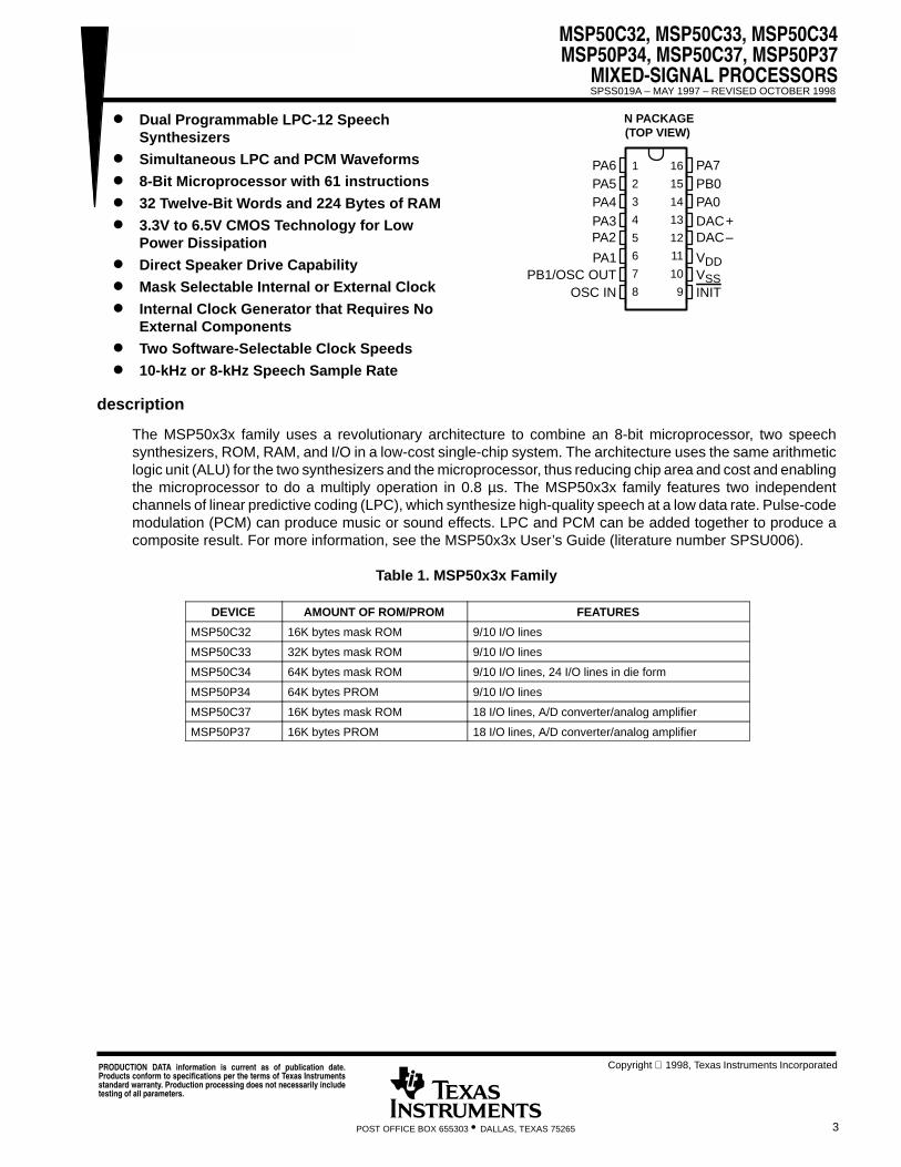
MSP50C32, MSP50C33, MSP50C34MSP50P34, MSP50C37, MSP50P37
MIXED-SIGNAL PROCESSORSSPSS019A – MAY 1997 – REVISED OCTOBER 1998
3POST OFFICE BOX 655303 • DALLAS, TEXAS 75265
Dual Programmable LPC-12 SpeechSynthesizers
Simultaneous LPC and PCM Waveforms
8-Bit Microprocessor with 61 instructions
32 Twelve-Bit Words and 224 Bytes of RAM
3.3V to 6.5V CMOS Technology for LowPower Dissipation
Direct Speaker Drive Capability
Mask Selectable Internal or External Clock
Internal Clock Generator that Requires NoExternal Components
Two Software-Selectable Clock Speeds
10-kHz or 8-kHz Speech Sample Rate
description
The MSP50x3x family uses a revolutionary architecture to combine an 8-bit microprocessor, two speechsynthesizers, ROM, RAM, and I/O in a low-cost single-chip system. The architecture uses the same arithmeticlogic unit (ALU) for the two synthesizers and the microprocessor, thus reducing chip area and cost and enablingthe microprocessor to do a multiply operation in 0.8 µs. The MSP50x3x family features two independentchannels of linear predictive coding (LPC), which synthesize high-quality speech at a low data rate. Pulse-codemodulation (PCM) can produce music or sound effects. LPC and PCM can be added together to produce acomposite result. For more information, see the MSP50x3x User’s Guide (literature number SPSU006).
Table 1. MSP50x3x Family
DEVICE AMOUNT OF ROM/PROM FEATURES
MSP50C32 16K bytes mask ROM 9/10 I/O lines
MSP50C33 32K bytes mask ROM 9/10 I/O lines
MSP50C34 64K bytes mask ROM 9/10 I/O lines, 24 I/O lines in die form
MSP50P34 64K bytes PROM 9/10 I/O lines
MSP50C37 16K bytes mask ROM 18 I/O lines, A/D converter/analog amplifier
MSP50P37 16K bytes PROM 18 I/O lines, A/D converter/analog amplifier
Copyright 1998, Texas Instruments IncorporatedPRODUCTION DATA information is current as of publication date.Products conform to specifications per the terms of Texas Instrumentsstandard warranty. Production processing does not necessarily includetesting of all parameters.
1
2
3
4
5
6
7
8
16
15
14
13
12
11
10
9
N PACKAGE(TOP VIEW)
OSC IN
PA6PA5PA4PA3PA2
PA1PB1/OSC OUT
PA7PB0PA0DAC+DAC–
VDDVSSINIT
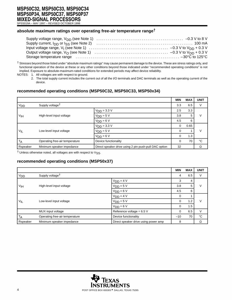
MSP50C32, MSP50C33, MSP50C34MSP50P34, MSP50C37, MSP50P37MIXED-SIGNAL PROCESSORSSPSS019A – MAY 1997 – REVISED OCTOBER 1998
4 POST OFFICE BOX 655303 • DALLAS, TEXAS 75265
absolute maximum ratings over operating free-air temperature range†
Supply voltage range, VDD (see Note 1) –0.3 V to 8 V. . . . . . . . . . . . . . . . . . . . . . . . . . . . . . . . . . . . . . . . . . . . . . Supply current, IDD or ISS (see Note 2) 100 mA. . . . . . . . . . . . . . . . . . . . . . . . . . . . . . . . . . . . . . . . . . . . . . . . . . . Input voltage range, VI (see Note 1) –0.3 V to VDD + 0.3 V. . . . . . . . . . . . . . . . . . . . . . . . . . . . . . . . . . . . . . . . . . Output voltage range, VO (see Note 1) –0.3 V to VDD + 0.3 V. . . . . . . . . . . . . . . . . . . . . . . . . . . . . . . . . . . . . . . Storage temperature range –30°C to 125°C. . . . . . . . . . . . . . . . . . . . . . . . . . . . . . . . . . . . . . . . . . . . . . . . . . . . . . .
† Stresses beyond those listed under “absolute maximum ratings” may cause permanent damage to the device. These are stress ratings only, andfunctional operation of the device at these or any other conditions beyond those indicated under “recommended operating conditions” is notimplied. Exposure to absolute-maximum-rated conditions for extended periods may affect device reliability.
NOTES: 1. All voltages are with respect to ground.2. The total supply current includes the current out of all the I/O terminals and DAC terminals as well as the operating current of the
device.
recommended operating conditions (MSP50C32, MSP50C33, MSP50x34)
MIN MAX UNIT
VDD Supply voltage† 3.3 6.5 V
VDD = 3.3 V 2.5 3.3
VIH High-level input voltage VDD = 5 V 3.8 5 V
VDD = 6 V 4.5 6
VDD = 3.3 V 0 0.65
VIL Low-level input voltage VDD = 5 V 0 1 V
VDD = 6 V 0 1.3
TA Operating free-air temperature Device functionality 0 70 °C
Rspeaker Minimum speaker impedance Direct speaker drive using 2 pin push-pull DAC option 32 Ω
† Unless otherwise noted, all voltages are with respect to VSS.
recommended operating conditions (MSP50x37)
MIN MAX UNIT
VDD Supply voltage† 4 6.5 V
VDD = 4 V 3 4
VIH High-level input voltage VDD = 5 V 3.8 5 V
VDD = 6 V 4.5 6
VDD = 4 V 0 1
VIL Low-level input voltage VDD = 5 V 0 1.2 V
VDD = 6 V 0 1.5
MUX input voltage Reference voltage = 6.5 V 0 6.5 V
TA Operating free-air temperature Device functionality –10 70 °C
Rspeaker Minimum speaker impedance Direct speaker drive using power amp 8 Ω
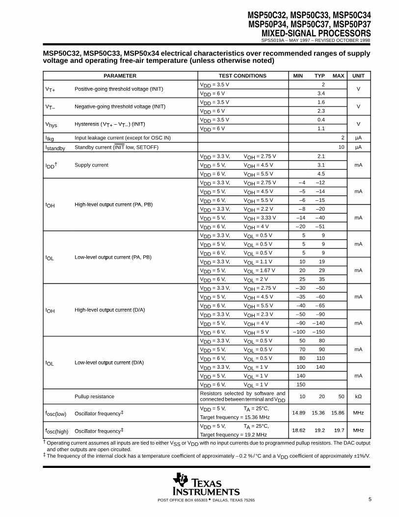
MSP50C32, MSP50C33, MSP50C34MSP50P34, MSP50C37, MSP50P37
MIXED-SIGNAL PROCESSORSSPSS019A – MAY 1997 – REVISED OCTOBER 1998
5POST OFFICE BOX 655303 • DALLAS, TEXAS 75265
MSP50C32, MSP50C33, MSP50x34 electrical characteristics over recommended ranges of supplyvoltage and operating free-air temperature (unless otherwise noted)
PARAMETER TEST CONDITIONS MIN TYP MAX UNIT
VT Positive going threshold voltage (INIT)VDD = 3.5 V 2
VVT+ Positive-going threshold voltage (INIT)VDD = 6 V 3.4
V
VT Negative going threshold voltage (INIT)VDD = 3.5 V 1.6
VVT– Negative-going threshold voltage (INIT)VDD = 6 V 2.3
V
Vh Hysteresis (VT VT ) (INIT)VDD = 3.5 V 0.4
VVhys Hysteresis (VT+ – VT– ) (INIT)VDD = 6 V 1.1
V
IIkg Input leakage current (except for OSC IN) 2 µA
Istandby Standby current (INIT low, SETOFF) 10 µA
†
VDD = 3.3 V, VOH = 2.75 V 2.1
IDD† Supply current VDD = 5 V, VOH = 4.5 V 3.1 mADDVDD = 6 V, VOH = 5.5 V 4.5
VDD = 3.3 V, VOH = 2.75 V –4 –12
VDD = 5 V, VOH = 4.5 V –5 –14 mA
IOH High level output current (PA PB)VDD = 6 V, VOH = 5.5 V –6 –15
IOH High-level output current (PA, PB)VDD = 3.3 V, VOH = 2.2 V –8 –20
VDD = 5 V, VOH = 3.33 V –14 –40 mA
VDD = 6 V, VOH = 4 V –20 –51
VDD = 3.3 V, VOL = 0.5 V 5 9
VDD = 5 V, VOL = 0.5 V 5 9 mA
IOL Low level output current (PA PB)VDD = 6 V, VOL = 0.5 V 5 9
IOL Low-level output current (PA, PB)VDD = 3.3 V, VOL = 1.1 V 10 19
VDD = 5 V, VOL = 1.67 V 20 29 mA
VDD = 6 V, VOL = 2 V 25 35
VDD = 3.3 V, VOH = 2.75 V –30 –50
VDD = 5 V, VOH = 4.5 V –35 –60 mA
IOH High level output current (D/A)VDD = 6 V, VOH = 5.5 V –40 –65
IOH High-level output current (D/A)VDD = 3.3 V, VOH = 2.3 V –50 –90
VDD = 5 V, VOH = 4 V –90 –140 mA
VDD = 6 V, VOH = 5 V –100 –150
VDD = 3.3 V, VOL = 0.5 V 50 80
VDD = 5 V, VOL = 0.5 V 70 90 mA
IOL Low level output current (D/A)VDD = 6 V, VOL = 0.5 V 80 110
IOL Low-level output current (D/A)VDD = 3.3 V, VOL = 1 V 100 140
VDD = 5 V, VOL = 1 V 140 mA
VDD = 6 V, VOL = 1 V 150
Pullup resistanceResistors selected by software andconnected between terminal and VDD
10 20 50 kΩ
f (l ) O ill t f ‡VDD = 5 V, TA = 25°C,
14 89 15 36 15 86 MHzfosc(low) Oscillator frequency‡Target frequency = 15.36 MHz
14.89 15.36 15.86 MHz
f (hi h) O ill t f ‡VDD = 5 V, TA = 25°C,
18 62 19 2 19 7 MHzfosc(high) Oscillator frequency‡Target frequency = 19.2 MHz
18.62 19.2 19.7 MHz
† Operating current assumes all inputs are tied to either VSS or VDD with no input currents due to programmed pullup resistors. The DAC outputand other outputs are open circuited.
‡ The frequency of the internal clock has a temperature coefficient of approximately –0.2 %/ °C and a VDD coefficient of approximately ±1%/V.
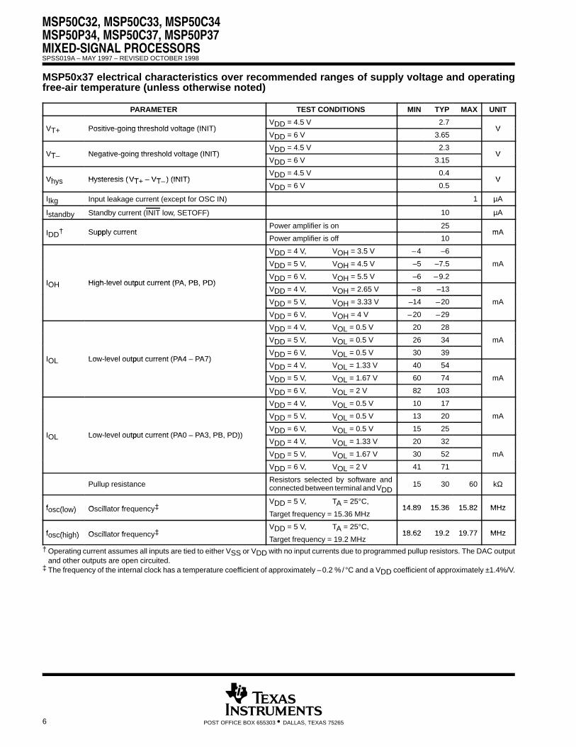
MSP50C32, MSP50C33, MSP50C34MSP50P34, MSP50C37, MSP50P37MIXED-SIGNAL PROCESSORSSPSS019A – MAY 1997 – REVISED OCTOBER 1998
6 POST OFFICE BOX 655303 • DALLAS, TEXAS 75265
MSP50x37 electrical characteristics over recommended ranges of supply voltage and operatingfree-air temperature (unless otherwise noted)
PARAMETER TEST CONDITIONS MIN TYP MAX UNIT
VT Positive going threshold voltage (INIT)VDD = 4.5 V 2.7
VVT+ Positive-going threshold voltage (INIT)VDD = 6 V 3.65
V
VT Negative going threshold voltage (INIT)VDD = 4.5 V 2.3
VVT– Negative-going threshold voltage (INIT)VDD = 6 V 3.15
V
Vh Hysteresis (VT VT ) (INIT)VDD = 4.5 V 0.4
VVhys Hysteresis (VT+ – VT– ) (INIT)VDD = 6 V 0.5
V
IIkg Input leakage current (except for OSC IN) 1 µA
Istandby Standby current (INIT low, SETOFF) 10 µA
I † Supply currentPower amplifier is on 25
mAIDD† Supply currentPower amplifier is off 10
mA
VDD = 4 V, VOH = 3.5 V –4 –6
VDD = 5 V, VOH = 4.5 V –5 –7.5 mA
IOH High level output current (PA PB PD)VDD = 6 V, VOH = 5.5 V –6 –9.2
IOH High-level output current (PA, PB, PD)VDD = 4 V, VOH = 2.65 V –8 –13
VDD = 5 V, VOH = 3.33 V –14 –20 mA
VDD = 6 V, VOH = 4 V –20 –29
VDD = 4 V, VOL = 0.5 V 20 28
VDD = 5 V, VOL = 0.5 V 26 34 mA
IOL Low level output current (PA4 PA7)VDD = 6 V, VOL = 0.5 V 30 39
IOL Low-level output current (PA4 – PA7)VDD = 4 V, VOL = 1.33 V 40 54
VDD = 5 V, VOL = 1.67 V 60 74 mA
VDD = 6 V, VOL = 2 V 82 103
VDD = 4 V, VOL = 0.5 V 10 17
VDD = 5 V, VOL = 0.5 V 13 20 mA
IOL Low level output current (PA0 PA3 PB PD))VDD = 6 V, VOL = 0.5 V 15 25
IOL Low-level output current (PA0 – PA3, PB, PD))VDD = 4 V, VOL = 1.33 V 20 32
VDD = 5 V, VOL = 1.67 V 30 52 mA
VDD = 6 V, VOL = 2 V 41 71
Pullup resistanceResistors selected by software andconnected between terminal and VDD
15 30 60 kΩ
f (l ) Oscillator freq enc ‡VDD = 5 V, TA = 25°C,
14 89 15 36 15 82 MHzfosc(low) Oscillator frequency‡Target frequency = 15.36 MHz
14.89 15.36 15.82 MHz
f (hi h) O ill t f ‡VDD = 5 V, TA = 25°C,
18 62 19 2 19 77 MHzfosc(high) Oscillator frequency‡Target frequency = 19.2 MHz
18.62 19.2 19.77 MHz
† Operating current assumes all inputs are tied to either VSS or VDD with no input currents due to programmed pullup resistors. The DAC outputand other outputs are open circuited.
‡ The frequency of the internal clock has a temperature coefficient of approximately –0.2 %/ °C and a VDD coefficient of approximately ±1.4%/V.
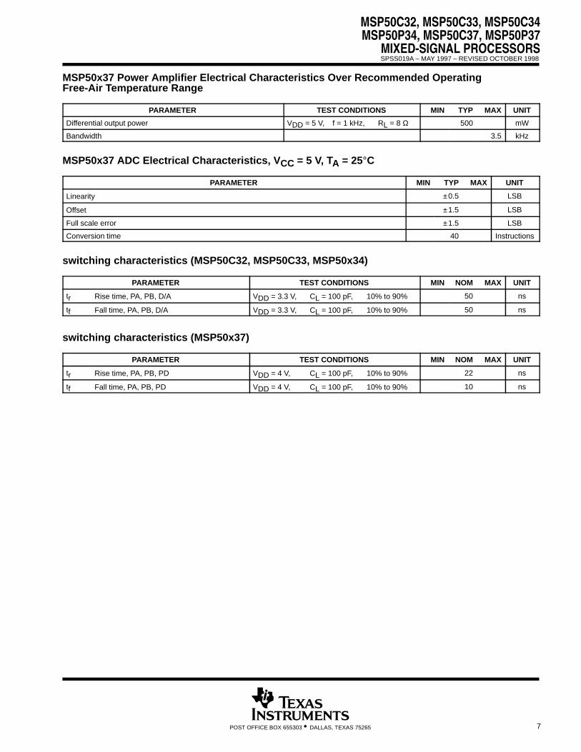
MSP50C32, MSP50C33, MSP50C34MSP50P34, MSP50C37, MSP50P37
MIXED-SIGNAL PROCESSORSSPSS019A – MAY 1997 – REVISED OCTOBER 1998
7POST OFFICE BOX 655303 • DALLAS, TEXAS 75265
MSP50x37 Power Amplifier Electrical Characteristics Over Recommended OperatingFree-Air Temperature Range
PARAMETER TEST CONDITIONS MIN TYP MAX UNIT
Differential output power VDD = 5 V, f = 1 kHz, RL = 8 Ω 500 mW
Bandwidth 3.5 kHz
MSP50x37 ADC Electrical Characteristics, VCC = 5 V, TA = 25°C
PARAMETER MIN TYP MAX UNIT
Linearity ±0.5 LSB
Offset ±1.5 LSB
Full scale error ±1.5 LSB
Conversion time 40 Instructions
switching characteristics (MSP50C32, MSP50C33, MSP50x34)
PARAMETER TEST CONDITIONS MIN NOM MAX UNIT
tr Rise time, PA, PB, D/A VDD = 3.3 V, CL = 100 pF, 10% to 90% 50 ns
tf Fall time, PA, PB, D/A VDD = 3.3 V, CL = 100 pF, 10% to 90% 50 ns
switching characteristics (MSP50x37)
PARAMETER TEST CONDITIONS MIN NOM MAX UNIT
tr Rise time, PA, PB, PD VDD = 4 V, CL = 100 pF, 10% to 90% 22 ns
tf Fall time, PA, PB, PD VDD = 4 V, CL = 100 pF, 10% to 90% 10 ns
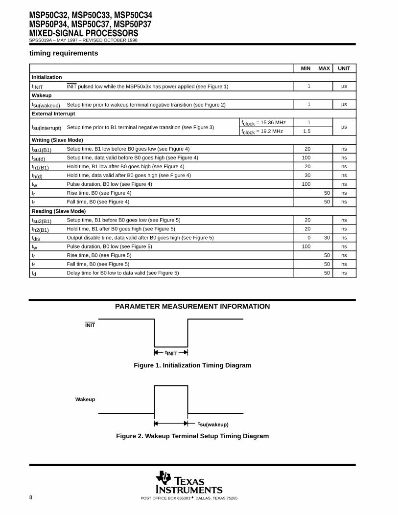
MSP50C32, MSP50C33, MSP50C34MSP50P34, MSP50C37, MSP50P37MIXED-SIGNAL PROCESSORSSPSS019A – MAY 1997 – REVISED OCTOBER 1998
8 POST OFFICE BOX 655303 • DALLAS, TEXAS 75265
timing requirements
MIN MAX UNIT
Initialization
tINIT INIT pulsed low while the MSP50x3x has power applied (see Figure 1) 1 µs
Wakeup
tsu(wakeup) Setup time prior to wakeup terminal negative transition (see Figure 2) 1 µs
External Interrupt
t (i t t) Setup time prior to B1 terminal negative transition (see Figure 3)fclock = 15.36 MHz 1
µstsu(interrupt) Setup time prior to B1 terminal negative transition (see Figure 3)fclock = 19.2 MHz 1.5
µs
Writing (Slave Mode)
tsu1(B1) Setup time, B1 low before B0 goes low (see Figure 4) 20 ns
tsu(d) Setup time, data valid before B0 goes high (see Figure 4) 100 ns
th1(B1) Hold time, B1 low after B0 goes high (see Figure 4) 20 ns
th(d) Hold time, data valid after B0 goes high (see Figure 4) 30 ns
tw Pulse duration, B0 low (see Figure 4) 100 ns
tr Rise time, B0 (see Figure 4) 50 ns
tf Fall time, B0 (see Figure 4) 50 ns
Reading (Slave Mode)
tsu2(B1) Setup time, B1 before B0 goes low (see Figure 5) 20 ns
th2(B1) Hold time, B1 after B0 goes high (see Figure 5) 20 ns
tdis Output disable time, data valid after B0 goes high (see Figure 5) 0 30 ns
tw Pulse duration, B0 low (see Figure 5) 100 ns
tr Rise time, B0 (see Figure 5) 50 ns
tf Fall time, B0 (see Figure 5) 50 ns
td Delay time for B0 low to data valid (see Figure 5) 50 ns
PARAMETER MEASUREMENT INFORMATION
tINIT
INIT
Figure 1. Initialization Timing Diagram
tsu(wakeup)
Wakeup
Figure 2. Wakeup Terminal Setup Timing Diagram
MSP50C32, MSP50C33, MSP50C34MSP50P34, MSP50C37, MSP50P37
MIXED-SIGNAL PROCESSORSSPSS019A – MAY 1997 – REVISED OCTOBER 1998
9POST OFFICE BOX 655303 • DALLAS, TEXAS 75265
PARAMETER MEASUREMENT INFORMATION
tsu(interrupt)
B1
Figure 3. External Interrupt Terminal Setup Timing Diagram
Data Valid
B1
B0
PA
tsu1(B1)
tw
th1(B1)
tftsu(d)
tr
th(d)
Figure 4. Write Timing Diagram (Slave Mode)
Data Valid
B1
B0
PA
tsu2(B1)
tw
th2(B1)
tf tr
tdistd
Figure 5. Read Timing Diagram (Slave Mode)

MSP50C32, MSP50C33, MSP50C34MSP50P34, MSP50C37, MSP50P37MIXED-SIGNAL PROCESSORSSPSS019A – MAY 1997 – REVISED OCTOBER 1998
10 POST OFFICE BOX 655303 • DALLAS, TEXAS 75265
Index
Index-1
AA register 2-11
A/D terminal select register 2-17
ABAAC (add B register to A register) instruction 4-7
ACAAC (add constant to A register) instruction 4-8
AGEC (A register greater than or equal to constant)instruction 4-9
ALU 2-11
AMAAC (add memory to A register) instruction 4-10
amplifier circuit 1-10
analog-to-digital converter MSP50x37 2-32
ANDCM (add a constant with memory) instruc-tion 4-11
ANEC (A register not equal to constant) instruc-tion 4-12
AORG directive assembler 3-16
applications 1-3
architecture 2-2 to 2-22
arithmetic logic unit. See ALU
arithmetic modes 5-45 to 5-48
assemblerAORG directive 3-16binary data 3-28binary object file 3-7BUNLIST option 3-20BYTE unlist option 3-4BYTE directive 3-16character strings 3-12command-line options 3-4 to 3-7command-line switches 3-4complete XREF switch 3-5 to 3-7COPY directive 3-16 to 3-18DATA directive 3-17DATA unlist option 3-5directives 3-14 to 3-27DUNLIST option 3-20END directive 3-17 to 3-19EQU directive 3-17error-to-screen switch 3-6expressions 3-13FUNLIST option 3-20IDT directive 3-18input files 3-7 to 3-9instruction count switch 3-6invoking 3-3LIST directive 3-18 to 3-20
assembler (continued)listing file 3-7listing file switch 3-6listing formats 3-27LSTST option 3-20macro switch 3-6MACRO/ENDM directive 3-25NARROW directive 3-19notation 3-2object module switch 3-6OBJUNL option 3-20OPTION directive 3-19 to 3-22output files 3-7 to 3-9PAGE directive 3-21page-eject switch 3-6PAGEOF option 3-20RBYTE directive 3-21 to 3-23RDATA directive 3-22RTEXT directive 3-22 to 3-24RXREF option 3-20SCRNOF option 3-20show usage switch 3-6source file 3-7source statement command field 3-8source statement comment field 3-9source statement contents 3-9 to 3-11source statement format 3-8 to 3-11source statement label field 3-8source statement operand field 3-9symbolic debugging switch 3-6symbols 3-11TABSIZE directive 3-26TEXT directive 3-23TEXT unlist option 3-5TITL directive 3-23 to 3-25TUNLST option 3-21UNL directive 3-24WARNING unlist option 3-5WARNOFF option 3-21WIDE directive 3-24XREF option 3-21XREF switch 3-5 to 3-7XREF unlist option 3-5
assembler source statementcommand field 3-8comment field 3-9constants 3-9 to 3-11label field 3-8operand field 3-9
Index
Index-2
AXCA (A register times to constant) instruction 4-13AXMA (A register times memory) instruction 4-14AXTM (A register times timer) instruction 4-15
BB register 2-12binary data assembler 3-28binary object file assembler 3-7BR (branch if status set) instruction 4-16BRA (branch always to address in A register)
instruction 4-17BUNLIST option assembler 3-20BYTE directive assembler 3-16BYTE unlist option assembler 3-4
CCALL (call subroutine if status set) instruction 4-18channel bit mode register 2 2-21channel scaling 2-25character strings assembler 3-12circuit
external clock interface 1-26four-transistor amplifier 1-10one-pin analog power amplifier output 1-14operational amplifier interface 1-10 1-13oscillator 1-26oversampling output filter 2-33power amplifier interface 1-11two-pin push pull power amplifier 1-14
CLA (clear A register) instruction 4-19CLB (clear B register) instruction 4-20clock select mask option 1-25clock select option
external clock interface 1-26oscillator circuit 1-26
clocks 2-30 to 2-32external 2-30external oscillator 2-30internal oscillator 2-30long interval monitor timer 2-31MSP50x37 2-31timer memory assignments 2-31
CLX (clear X register) instruction 4-21coding synthesizer 5-2 to 5-5
command field assembler source statement 3-8comment field assembler source statement 3-9complete XREF switch assembler 3-5 to 3-7constants assembler source statement 3-9 to 3-11conversion start register 2-17COPY directive assembler 3-16 to 3-18
DD/A options 1-8 to 1-15
four-transistor amplifier circuit 1-10MSP50C32 1-8MSP50C33 1-8MSP50C34 1-8MSP50C37 1-8MSP50P34 1-8MSP50P37 1-8operational amplifier interface circuit 1-10, 1-13option 1 1-8 to 1-12option 1 output waveforms 1-9option 2 1-12 to 1-15option 2 output waveforms 1-12power amplifier interface circuit 1-11single-pin doubled-ended 1-12 to 1-15single-pin double-ended output waveforms 1-12two-pin push pull 1-8 to 1-12two-pin push pull output waveforms 1-9
DAC option 1-26data direction register 2-17DATA directive assembler 3-17data input register 2-17data output register 2-17data sheet E-2 to E-11DATA unlist option assembler 3-5DDR register 2-17DECMN (decrement memory) instruction 4-22decoding synthesizer 5-2 to 5-5DECXN (decrement X register) instruction 4-23development cycle 6-2development tools
EMU50C3x A-6MSD50C3x A-6OTP-PROG2 A-7speech A-5 to A-8WINSDS A-5
diagramfunctional block 1-4MSP50x37 functional block 1-5
Index
Index-3
diagram (continued)MSP50x37 system block 2-4system block 2-3
die pad locationsMSP50C32 1-17MSP50C33 1-17MSP50x34 1-20
digital-to-analog converter 2-26DIR register 2-17directive
AORG 3-16BYTE 3-16COPY 3-16 to 3-18DATA 3-17END 3-17 to 3-19EQU 3-17IDT 3-18LIST 3-18 to 3-20MARCO/ENDM 3-25NARROW 3-19OPTION 3-19 to 3-22PAGE 3-21RBYTE 3-21 to 3-23RDATA 3-22RTEXT 3-22 to 3-24TABSIZE 3-26TEXT 3-23TITL 3-23 to 3-25UNL 3-24WIDE 3-24
directives assembler 3-14 to 3-27DOR register 2-17dual synthesis program C-2 to C-51DUNLIST option assembler 3-20DW package mechanical information 6-8, 6-9
EEMU50C3x speech development tool A-6ENA1 bit mode register 1 2-20ENA2 bit mode register 1 2-20END directive assembler 3-17 to 3-19EQU directive assembler 3-17error-to-screen switch assembler 3-6external clock 2-30external clock interface 1-26external oscillator 2-30
EXTSG (change to extended-sign mode) instruc-tion 4-24
Ffeatures 1-6
MSP50C32 1-2MSP50C33 1-2MSP50C34 1-2MSP50C37 1-2MSP50P34 1-2MSP50P37 1-2MSP50x32 1-6MSP50x33 1-6MSP50x34 1-6MSP50x37 1-7
forms new product release 6-11 to 6-21four-transistor amplifier circuit 1-10frame length control 2-26functional block diagram 1-4
MSP50x37 1-5functional description 1-4FUNLIST option assembler 3-20
GGET (get data from RAM/ROM) instruction 4-25GET instruction
from internal RAM 5-56 to 5-58from internal ROM 5-55 to 5-57use of 5-54 to 5-58
II/O map bit mode register 2 2-21I/O registers 2-17IAC (increment A register) instruction 4-27IBC (increment B register) instruction 4-28IDT directive assembler 3-18INCMC (increment memory) instruction 4-29initialization 2-29input ports 2-17 to 2-19instruction count switch assembler 3-6instruction opcodes 4-6instruction set 4-3 to 4-6instruction syntax 4-2integer mode flag 2-13
Index
Index-4
internal oscillator 2-30SPEED bit 2-30
interrupts 2-27 to 2-29level 1 2-27 to 2-29level 2 2-27 to 2-29LPC1 bit 2-27PCM1 bit 2-27
INTGR (change to integer mode) instruction 4-30IXC (increment X register) instruction 4-31
Llabel field assembler source statement 3-8linear predictive coding. See LPCLIST directive assembler 3-18 to 3-20listing file assembler 3-7listing file switch assembler 3-6listing formats assembler 3-27long interval monitor timer 2-31low pass filter 2-25LPC 1-23
data compression 1-24generating speech and tones 5-60model 1-23synthesizer mode 1 2-22 to 2-24vocal-tract model diagram 1-24
LPC editing A-3 to A-5LPC1 bit mode register 1 2-20LPC12 1-4LPC2 bit mode register 2 2-21LSTST option assembler 3-20LUAA (look-up with A register) instruction 4-32LUAB (look-up with B register) instruction 4-33LUAPS (indirect look-up with A register) instruc-
tion 4-34
Mmacro switch assembler 3-6MACRO/ENDM directive assembler 3-25mask options 1-25
clock select option 1-25clock select option external clock interface 1-26clock select option oscillator circuit 1-26DAC option 1-26power amplifier 1-27
mechanical information 6-4 to 6-9DW package 6-8, 6-9N package 6-4, 6-5, 6-6NW package 6-4, 6-7
memory-mapped registers 2-9 to 2-11mode
power savings 5-49slave 5-50 to 5-54sleep 2-30, 5-49standby 2-29, 5-49
mode register 1 2-19 to 2-21bit description 2-20ENA1 bit 2-20ENA2 bit 2-20LPC1 bit 2-20PCM1 bit 2-20RAMROM bit 2-20slave bit 2-20unvoice1 bit 2-20
mode register 2 2-20 to 2-22bit descriptions 2-21channel bit 2-21I/O map bit 2-21LPC2 bit 2-21PCM2 bit 2-21PPC1 bit 2-21PPC2 bit 2-21speed bit 2-21unvoice2 bit 2-21
Mode registers 2-19 to 2-22MSD50C3x speech development tools A-6MSP50C32
D/A options 1-8die pad locations 1-17features 1-2
MSP50C33D/A options 1-8die pad locations 1-17features 1-2
MSP50C34D/A options 1-8features 1-2NW package terminal assignments 1-18
MSP50C37additional features 1-4applications 1-3D/A options 1-8features 1-2power amplifier option 1-27
Index
Index-5
MSP50P34D/A options 1-8features 1-2NW package terminal assignments 1-18signal descriptions 1-19
MSP50P37additional features 1-4applications 1-3D/A options 1-8features 1-2
MSP50x32DW package terminal assignments 1-15 to 1-17features 1-6N package terminal assignments 1-15 to 1-17RAM map 2-7
MSP50x33DW package terminal assignments 1-15 to 1-17features 1-6N package terminal assignments 1-15 to 1-17RAM map 2-7
MSP50x34die pad locations 1-20DW package terminal assignments 1-15 to 1-17features 1-6N package terminal assignments 1-15 to 1-17RAM map 2-7
MSP50x37A/D terminal select register 2-17analog-to-digital converter 2-32conversion start register 2-17DW package terminal assignments 1-21features 1-7functional block diagram 1-5long interval monitor timer 2-31N package terminal assignments 1-21one-pin analog 1-14oversampling output filter circuit 2-33power amplifier 2-33power amplifier circuit 1-13 to 1-15RAM map 2-8 to 2-10signal descriptions 1-22speaker driver 1-8 to 1-12system block diagram 2-4timer RAM assignments 2-31two-pin push pull option 1-14
multiplication instruction 5-48
NN package mechanical information 6-4, 6-5, 6-6
NARROW directive assembler 3-19
new product release forms 6-11 to 6-21
NW package mechanical information 6-4, 6-7
Oobject module switch assembler 3-6
OBJUNL option assembler 3-20
Off synthesizer mode 0 2-22
one-pin analogMSP50x37 1-14power amplifier circuit 1-14
opcode instructions 4-6
operand field assembler source statement 3-9
operational amplifier interface circuit 1-10, 1-13
option 1D/A option 1-8 to 1-12four-transistor amplifier circuit 1-10operational amplifier interface circuit 1-10output waveforms 1-9power amplifier interface circuit 1-11speaker driver 1-8 to 1-12two-pin push pull 1-8
option 2D/A option 1-12 to 1-15operational amplifier interface circuit 1-13output waveforms 1-12single-pin doubled-ended 1-12 to 1-15
OPTION directive assembler 3-19 to 3-22
ORCM (OR constant with memory) instruction 4-35
ordering information 6-10
oscillatorexternal 2-30internal 2-30
oscillator circuit 1-26
OTP-PROG2 speech development tools A-7
output filter circuit MSP50x37 2-33
output ports 2-17 to 2-19
oversampling output filter circuit 2-25
Index
Index-6
PPAGE directive assembler 3-21
page-eject switch assembler 3-6PAGEOF option assembler 3-20parallel-to-serial register 2-16PCM
generating speech and tones 5-60generating tones 5-58 to 5-60synthesizer mode 2 2-23
PCM excited LPC synthesizer mode 3 2-23PCM1 bit mode register 1 2-20PCM2 bit mode register 2 2-21PER register 2-17pitch period counter 2-14 to 2-16
pitch register 2-14 to 2-16ports input and output 2-17 to 2-19power amplifier MSP50x37 2-33power amplifier circuit
MSP50x37 1-13 to 1-15one-pin analog 1-14two-pin push pull option 1-14
power amplifier interface circuit 1-11power amplifier option 1-27power control 2-29power-savings modes 5-49power-up initialization circuit 1-17
PPC 2-14 to 2-16PPC1 bit mode register 2 2-21PPC2 bit mode register 2 2-21program
dual synthesis 5-12 to 5-45 C-2 to C-51synthesis D-2 to D-31
program counter 2-5program counter stack 2-6
pullup enable register 2-17
RRAM 2-6
map for MSP50x32 2-7map for MSP50x33 2-7map for MSP50x34 2-7map for MSP50x37 2-8 to 2-10synthesizer use of 2-23 to 2-25
RAM (continued)use by synthesizer 5-4 to 5-9
RAMROM bit mode register 1 2-20RBYTE directive assembler 3-21 to 3-23RDATA directive assembler 3-22register
A 2-11A/D terminal select 2-17B 2-12conversion start 2-17data direction 2-17data input 2-17data output 2-17DDR 2-17DIR 2-17DOR 2-17I/O 2-17mode 2-19 to 2-22mode register 1 2-19 to 2-21mode register 1 bit descriptions 2-20mode register 2 2-20 to 2-22mode register 2 bit descriptions 2-21parallel-to-serial 2-16PER 2-17pitch 2-14 to 2-16pullup enable 2-17SAR 2-16speech address 2-16timer 2-13timer prescale 2-14X 2-12
RETI (return from interrupt) instruction 4-36RETN (return from subroutine) instruction 4-37ROM 2-4 to 2-6
locations 2-5use by synthesizer 5-8
RTEXT directive assembler 3-22 to 3-24RXREF option assembler 3-20
SSALA (shift A register) instruction 4-38SALA4 (shift A register left four bits) instruction 4-39SAR 2-16SARA (shift A register right one bit) instruction 4-40SBAAN (subtract B register from A register) instruc-
tion 4-41SBR (short branch if status set) instruction 4-42
Index
Index-7
script generation A-2 to A-5LPC editing A-3 to A-5pitfalls A-4speaker selection A-2speech collection A-2 to A-4
SCRNOF option assembler 3-20SETOFF standby mode 2-29SETOFF (set processor to OFF mode) instruc-
tion 4-43show usage switch assembler 3-6signal descriptions 1-15 to 1-23
MSP50P34 1-19MSP50x37 1-22
single-pin doubled-ended D/A option 1-12 to 1-15single-pin double-ended
operational amplifier interface circuit 1-13output waveforms 1-12
slave bit mode register 1 2-20slave mode 5-50 to 5-54
read operation 5-52 to 5-54write operation 5-51 to 5-53
sleep mode 2-30 5-49SMAAN (subtract memory from A register) instruc-
tion 4-44source file assembler 3-7source statement
command field 3-8comment field 3-9contents 3-9 to 3-11label field 3-8operand field 3-9
source statement format assembler 3-8 to 3-11speaker driver 1-8 to 1-12speaker selection A-2speech address register 2-16speech collection A-2 to A-4speech development 6-3speech development tools A-5 to A-8speech production sequence 6-3speech synthesis 2-22 to 2-27SPEED bit internal oscillator 2-30speed bit mode register 2 2-21standby mode 2-29, 5-49
SETOFF instruction 2-29status flag 2-12symbolic debugging switch assembler 3-6
synthesis program D-2 to D-31synthesizer
channel scaling 2-25coding and decoding 5-2 to 5-5digital-to-analog converter 2-26frame length control 2-26low pass filter 2-25oversampling output filter 2-25program frame-update routine 5-11program initialization 5-9program interpolation routine 5-10program phrase selection 5-9program speech initialization 5-9RAM usages 5-4 to 5-9RAM use by 2-23 to 2-25ROM usages 5-8
synthesizer control 5-2 to 5-10synthesizer mode 0 2-22synthesizer mode 1 2-22 to 2-24synthesizer mode 2 2-23synthesizer mode 3 2-23synthesizer program 5-12 to 5-45
frame-update routine 5-11initialization 5-9interpolation routine 5-10phrase selection 5-9speech initialization 5-9
system block diagram 2-3MSP50x37 2-4
TTAB (transfer A register to B register) instruc-
tion 4-45TABSIZE directive assembler 3-26TAM (transfer A register to memory) instruction 4-46TAMD (transfer A register to memory direct) instruc-
tion 4-47TAMIX (transfer A register to memory and increment
X register) instruction 4-48TAMODE (transfer A register to mode register 1)
instruction 4-49TAPSC (transfer A register to prescale register)
instruction 4-50TASYN (transfer A register to synthesizer register)
instruction 4-51TATM (transfer A register to timer register) instruc-
tion 4-53
Index
Index-8
TAX (transfer A register to X register) instruc-tion 4-54
TBM (transfer B register to memory) instruction 4-55
TCA (transfer constant to A register) instruction 4-56
TCX (transfer constant to X register) instruction 4-57
terminal assignments 1-15 to 1-23MSP50C34 1-18MSP50P34 1-18MSP50x32 1-15 to 1-17MSP50x33 1-15 to 1-17MSP50x34 1-15 to 1-17MSP50x37 1-21NW package 1-18
TEXT directive assembler 3-23
TEXT unlist option assembler 3-5
timerlong interval monitor 2-31MSP50x37 2-31RAM assignments 2-31
timer prescale register 2-14
timer register 2-13
TITL directive assembler 3-23 to 3-25
TMA (transfer memory to A register) instruction 4-58
TMAD (transfer memory to A register) instruc-tion 4-59
TMAIX (transfer memory to A register and incrementX register) instruction 4-60
TMXD (transfer memory directly to X register)instruction 4-61
tones generating using PCM 5-58 to 5-60
TRNDA (transfer random number into A register)instruction 4-62
TSP50C1xsummary of changes from B-2upgrading from B-3 to B-7
TSTCA (test constant with A register) instruc-tion 4-63
TSTCM (test constant with memory) instruction 4-64
TTMA (transfer timer register to A register) instruc-tion 4-65
TUNLST option assembler 3-21
two-pin push pullD/A option 1-8 to 1-12output waveforms 1-9
two-pin push pull optionfour-transistor amplifier circuit 1-10MSP50x37 1-14operational amplifier interface circuit 1-10power amplifier circuit 1-14power amplifier interface circuit 1-11
TXA (transfer X register to A register) instruc-tion 4-66
UUNL directive assembler 3-24unvoice1 bit mode register 1 2-20unvoice2 bit mode register 2 2-21
Vvocal tract 1-23
WWARNING unlist option assembler 3-5WARNOFF option assembler 3-21WIDE directive assembler 3-24WINSDS speech development tools A-5
XX register 2-12XBA (exchange contents of B register and A regis-
ter) instruction 4-67XBX (exchange contents of B register and X regis-
ter) instruction 4-68XGEC (X register greater than or equal to constant)
instruction 4-69XREF option assembler 3-21XREF switch assembler 3-5 to 3-7XREF unlist option assembler 3-5