mpc8347e powerquicc™ ii pro integrated host … sheets/freescale semi...802.3ac® standards —...
TRANSCRIPT
© Freescale Semiconductor, Inc., 2005–2009. All rights reserved.
Freescale SemiconductorTechnical Data
The MPC8347E PowerQUICC™ II Pro is a next generation PowerQUICC II integrated host processor. The MPC8347E contains a PowerPC™ processor core built on Power Architecture™ technology with system logic for networking, storage, and general-purpose embedded applications. For functional characteristics of the processor, refer to the MPC8349E PowerQUICC™ II Pro Integrated Host Processor Family Reference Manual.
To locate published errata or updates for this document, refer to the MPC8347E product summary page on our website listed on the back cover of this document or, contact your local Freescale sales office.
NOTE The information in this document is accurate for revision 1.1 silicon and earlier. For information on revision 3.0 silicon and later versions (for orderable part numbers ending in A or B), see the MPC8347EA PowerQUICC™ II Pro Integrated Host Processor Hardware Specifications.
See Section 23.1, “Part Numbers Fully Addressed by This Document,” for silicon revision level determination.
Document Number: MPC8347EECRev. 11, 02/2009
Contents1. Overview . . . . . . . . . . . . . . . . . . . . . . . . . . . . . . . . . . . 22. Electrical Characteristics . . . . . . . . . . . . . . . . . . . . . . 73. Power Characteristics . . . . . . . . . . . . . . . . . . . . . . . . 104. Clock Input Timing . . . . . . . . . . . . . . . . . . . . . . . . . . 125. RESET Initialization . . . . . . . . . . . . . . . . . . . . . . . . . 136. DDR SDRAM . . . . . . . . . . . . . . . . . . . . . . . . . . . . . . 157. DUART . . . . . . . . . . . . . . . . . . . . . . . . . . . . . . . . . . . 218. Ethernet: Three-Speed Ethernet, MII Management . 229. USB . . . . . . . . . . . . . . . . . . . . . . . . . . . . . . . . . . . . . . 33
10. Local Bus . . . . . . . . . . . . . . . . . . . . . . . . . . . . . . . . . 3511. JTAG . . . . . . . . . . . . . . . . . . . . . . . . . . . . . . . . . . . . . 4212. I2C . . . . . . . . . . . . . . . . . . . . . . . . . . . . . . . . . . . . . . . 4513. PCI . . . . . . . . . . . . . . . . . . . . . . . . . . . . . . . . . . . . . . 4714. Timers . . . . . . . . . . . . . . . . . . . . . . . . . . . . . . . . . . . . 5015. GPIO . . . . . . . . . . . . . . . . . . . . . . . . . . . . . . . . . . . . . 5116. IPIC . . . . . . . . . . . . . . . . . . . . . . . . . . . . . . . . . . . . . . 5217. SPI . . . . . . . . . . . . . . . . . . . . . . . . . . . . . . . . . . . . . . . 5318. Package and Pin Listings . . . . . . . . . . . . . . . . . . . . . 5519. Clocking . . . . . . . . . . . . . . . . . . . . . . . . . . . . . . . . . . 7620. Thermal . . . . . . . . . . . . . . . . . . . . . . . . . . . . . . . . . . . 8421. System Design Information . . . . . . . . . . . . . . . . . . . 9122. Document Revision History . . . . . . . . . . . . . . . . . . . 9523. Ordering Information . . . . . . . . . . . . . . . . . . . . . . . . 98
MPC8347E PowerQUICC™ II ProIntegrated Host Processor Hardware Specifications
MPC8347E PowerQUICC™ II Pro Integrated Host Processor Hardware Specifications, Rev. 11
2 Freescale Semiconductor
Overview
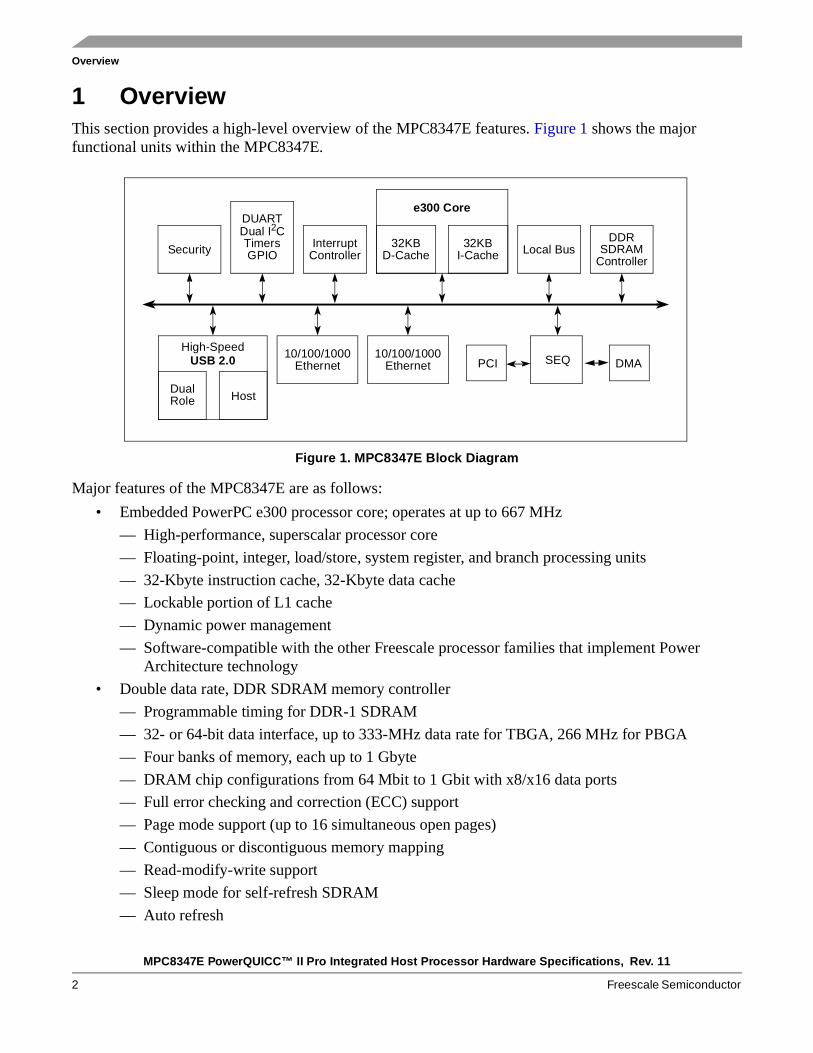
1 OverviewThis section provides a high-level overview of the MPC8347E features. Figure 1 shows the major functional units within the MPC8347E.
Figure 1. MPC8347E Block Diagram
Major features of the MPC8347E are as follows:
• Embedded PowerPC e300 processor core; operates at up to 667 MHz
— High-performance, superscalar processor core
— Floating-point, integer, load/store, system register, and branch processing units
— 32-Kbyte instruction cache, 32-Kbyte data cache
— Lockable portion of L1 cache
— Dynamic power management
— Software-compatible with the other Freescale processor families that implement Power Architecture technology
• Double data rate, DDR SDRAM memory controller
— Programmable timing for DDR-1 SDRAM
— 32- or 64-bit data interface, up to 333-MHz data rate for TBGA, 266 MHz for PBGA
— Four banks of memory, each up to 1 Gbyte
— DRAM chip configurations from 64 Mbit to 1 Gbit with x8/x16 data ports
— Full error checking and correction (ECC) support
— Page mode support (up to 16 simultaneous open pages)
— Contiguous or discontiguous memory mapping
— Read-modify-write support
— Sleep mode for self-refresh SDRAM
— Auto refresh
DUARTDual I2CTimersGPIOSecurity Interrupt
Controller
DualRole
High-Speed
Local BusDDR
SDRAMController
Host
32KBD-Cache
e300 Core
32KBI-Cache
USB 2.0 10/100/1000 SEQPCI DMAEthernet10/100/1000
Ethernet
MPC8347E PowerQUICC™ II Pro Integrated Host Processor Hardware Specifications, Rev. 11
Freescale Semiconductor 3
Overview
— On-the-fly power management using CKE
— Registered DIMM support
— 2.5-V SSTL2 compatible I/O
• Dual three-speed (10/100/1000) Ethernet controllers (TSECs)
— Dual controllers designed to comply with IEEE 802.3®, 802.3u®, 820.3x®, 802.3z®, 802.3ac® standards
— Ethernet physical interfaces:
– 1000 Mbps IEEE Std. 802.3 GMII/RGMII, IEEE Std. 802.3z TBI/RTBI, full-duplex
– 10/100 Mbps IEEE Std. 802.3 MII full- and half-duplex
— Buffer descriptors are backward-compatible with MPC8260 and MPC860T 10/100 programming models
— 9.6-Kbyte jumbo frame support
— RMON statistics support
— Internal 2-Kbyte transmit and 2-Kbyte receive FIFOs per TSEC module
— MII management interface for control and status
— Programmable CRC generation and checking
• PCI interface
— Designed to comply with PCI Specification Revision 2.2
— Data bus width:
– 32-bit data PCI interface operating at up to 66 MHz
— PCI 3.3-V compatible
— PCI host bridge capabilities
— PCI agent mode on PCI interface
— PCI-to-memory and memory-to-PCI streaming
— Memory prefetching of PCI read accesses and support for delayed read transactions
— Posting of processor-to-PCI and PCI-to-memory writes
— On-chip arbitration supporting five masters on PCI
— Accesses to all PCI address spaces
— Parity supported
— Selectable hardware-enforced coherency
— Address translation units for address mapping between host and peripheral
— Dual address cycle for target
— Internal configuration registers accessible from PCI
• Security engine is optimized to handle all the algorithms associated with IPSec, SSL/TLS, SRTP, IEEE Std. 802.11i®, iSCSI, and IKE processing. The security engine contains four crypto-channels, a controller, and a set of crypto execution units (EUs):
— Public key execution unit (PKEU) :
– RSA and Diffie-Hellman algorithms
MPC8347E PowerQUICC™ II Pro Integrated Host Processor Hardware Specifications, Rev. 11
4 Freescale Semiconductor
Overview
– Programmable field size up to 2048 bits
– Elliptic curve cryptography
– F2m and F(p) modes
– Programmable field size up to 511 bits
— Data encryption standard (DES) execution unit (DEU)
– DES and 3DES algorithms
– Two key (K1, K2) or three key (K1, K2, K3) for 3DES
– ECB and CBC modes for both DES and 3DES
— Advanced encryption standard unit (AESU)
– Implements the Rijndael symmetric-key cipher
– Key lengths of 128, 192, and 256 bits
– ECB, CBC, CCM, and counter (CTR) modes
— ARC four execution unit (AFEU)
– Stream cipher compatible with the RC4 algorithm
– 40- to 128-bit programmable key
— Message digest execution unit (MDEU)
– SHA with 160- or 256-bit message digest
– MD5 with 128-bit message digest
– HMAC with either algorithm
— Random number generator (RNG)
— Four crypto-channels, each supporting multi-command descriptor chains
– Static and/or dynamic assignment of crypto-execution units through an integrated controller
– Buffer size of 256 bytes for each execution unit, with flow control for large data sizes
• Universal serial bus (USB) dual role controller
— USB on-the-go mode with both device and host functionality
— Complies with USB specification Rev. 2.0
— Can operate as a stand-alone USB device
– One upstream facing port
– Six programmable USB endpoints
— Can operate as a stand-alone USB host controller
– USB root hub with one downstream-facing port
– Enhanced host controller interface (EHCI) compatible
– High-speed (480 Mbps), full-speed (12 Mbps), and low-speed (1.5 Mbps) operations
— External PHY with UTMI, serial and UTMI+ low-pin interface (ULPI)
• Universal serial bus (USB) multi-port host controller
— Can operate as a stand-alone USB host controller
– USB root hub with one or two downstream-facing ports
MPC8347E PowerQUICC™ II Pro Integrated Host Processor Hardware Specifications, Rev. 11
Freescale Semiconductor 5
Overview
– Enhanced host controller interface (EHCI) compatible
– Complies with USB Specification Rev. 2.0
— High-speed (480 Mbps), full-speed (12 Mbps), and low-speed (1.5 Mbps) operations
— Direct connection to a high-speed device without an external hub
— External PHY with serial and low-pin count (ULPI) interfaces
• Local bus controller (LBC)
— Multiplexed 32-bit address and data operating at up to 133 MHz
— Four chip selects support four external slaves
— Up to eight-beat burst transfers
— 32-, 16-, and 8-bit port sizes controlled by an on-chip memory controller
— Three protocol engines on a per chip select basis:
– General-purpose chip select machine (GPCM)
– Three user-programmable machines (UPMs)
– Dedicated single data rate SDRAM controller
— Parity support
— Default boot ROM chip select with configurable bus width (8-, 16-, or 32-bit)
• Programmable interrupt controller (PIC)
— Functional and programming compatibility with the MPC8260 interrupt controller
— Support for 8 external and 35 internal discrete interrupt sources
— Support for 1 external (optional) and 7 internal machine checkstop interrupt sources
— Programmable highest priority request
— Four groups of interrupts with programmable priority
— External and internal interrupts directed to host processor
— Redirects interrupts to external INTA pin in core disable mode.
— Unique vector number for each interrupt source
• Dual industry-standard I2C interfaces
— Two-wire interface
— Multiple master support
— Master or slave I2C mode support
— On-chip digital filtering rejects spikes on the bus
— System initialization data optionally loaded from I2C-1 EPROM by boot sequencer embedded hardware
• DMA controller
— Four independent virtual channels
— Concurrent execution across multiple channels with programmable bandwidth control
— All channels accessible to local core and remote PCI masters
— Misaligned transfer capability
MPC8347E PowerQUICC™ II Pro Integrated Host Processor Hardware Specifications, Rev. 11
6 Freescale Semiconductor
Overview
— Data chaining and direct mode
— Interrupt on completed segment and chain
• DUART
— Two 4-wire interfaces (RxD, TxD, RTS, CTS)
— Programming model compatible with the original 16450 UART and the PC16550D
• Serial peripheral interface (SPI) for master or slave
• General-purpose parallel I/O (GPIO)
— 52 parallel I/O pins multiplexed on various chip interfaces
• System timers
— Periodic interrupt timer
— Real-time clock
— Software watchdog timer
— Eight general-purpose timers
• Designed to comply with IEEE Std. 1149.1™, JTAG boundary scan
• Integrated PCI bus and SDRAM clock generation
MPC8347E PowerQUICC™ II Pro Integrated Host Processor Hardware Specifications, Rev. 11
Freescale Semiconductor 7
Electrical Characteristics
2 Electrical CharacteristicsThis section provides the AC and DC electrical specifications and thermal characteristics for the MPC8347E. The MPC8347E is currently targeted to these specifications. Some of these specifications are independent of the I/O cell, but are included for a more complete reference. These are not purely I/O buffer design specifications.
2.1 Overall DC Electrical CharacteristicsThis section covers the ratings, conditions, and other characteristics.
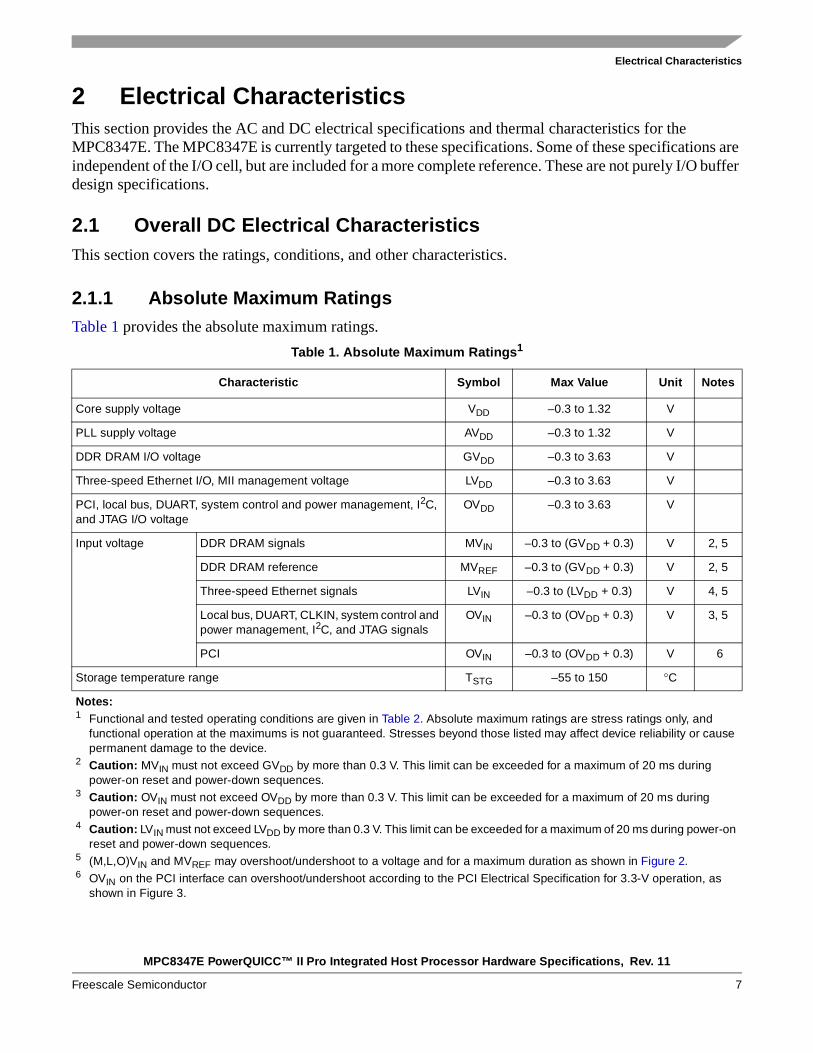
2.1.1 Absolute Maximum RatingsTable 1 provides the absolute maximum ratings.
Table 1. Absolute Maximum Ratings1
Characteristic Symbol Max Value Unit Notes
Core supply voltage VDD –0.3 to 1.32 V
PLL supply voltage AVDD –0.3 to 1.32 V
DDR DRAM I/O voltage GVDD –0.3 to 3.63 V
Three-speed Ethernet I/O, MII management voltage LVDD –0.3 to 3.63 V
PCI, local bus, DUART, system control and power management, I2C, and JTAG I/O voltage
OVDD –0.3 to 3.63 V
Input voltage DDR DRAM signals MVIN –0.3 to (GVDD + 0.3) V 2, 5
DDR DRAM reference MVREF –0.3 to (GVDD + 0.3) V 2, 5
Three-speed Ethernet signals LVIN –0.3 to (LVDD + 0.3) V 4, 5
Local bus, DUART, CLKIN, system control and power management, I2C, and JTAG signals
OVIN –0.3 to (OVDD + 0.3) V 3, 5
PCI OVIN –0.3 to (OVDD + 0.3) V 6
Storage temperature range TSTG –55 to 150 °C
Notes: 1 Functional and tested operating conditions are given in Table 2. Absolute maximum ratings are stress ratings only, and
functional operation at the maximums is not guaranteed. Stresses beyond those listed may affect device reliability or cause permanent damage to the device.
2 Caution: MVIN must not exceed GVDD by more than 0.3 V. This limit can be exceeded for a maximum of 20 ms during power-on reset and power-down sequences.
3 Caution: OVIN must not exceed OVDD by more than 0.3 V. This limit can be exceeded for a maximum of 20 ms during power-on reset and power-down sequences.
4 Caution: LVIN must not exceed LVDD by more than 0.3 V. This limit can be exceeded for a maximum of 20 ms during power-on reset and power-down sequences.
5 (M,L,O)VIN and MVREF may overshoot/undershoot to a voltage and for a maximum duration as shown in Figure 2. 6 OVIN on the PCI interface can overshoot/undershoot according to the PCI Electrical Specification for 3.3-V operation, as
shown in Figure 3.
MPC8347E PowerQUICC™ II Pro Integrated Host Processor Hardware Specifications, Rev. 11
8 Freescale Semiconductor
Electrical Characteristics
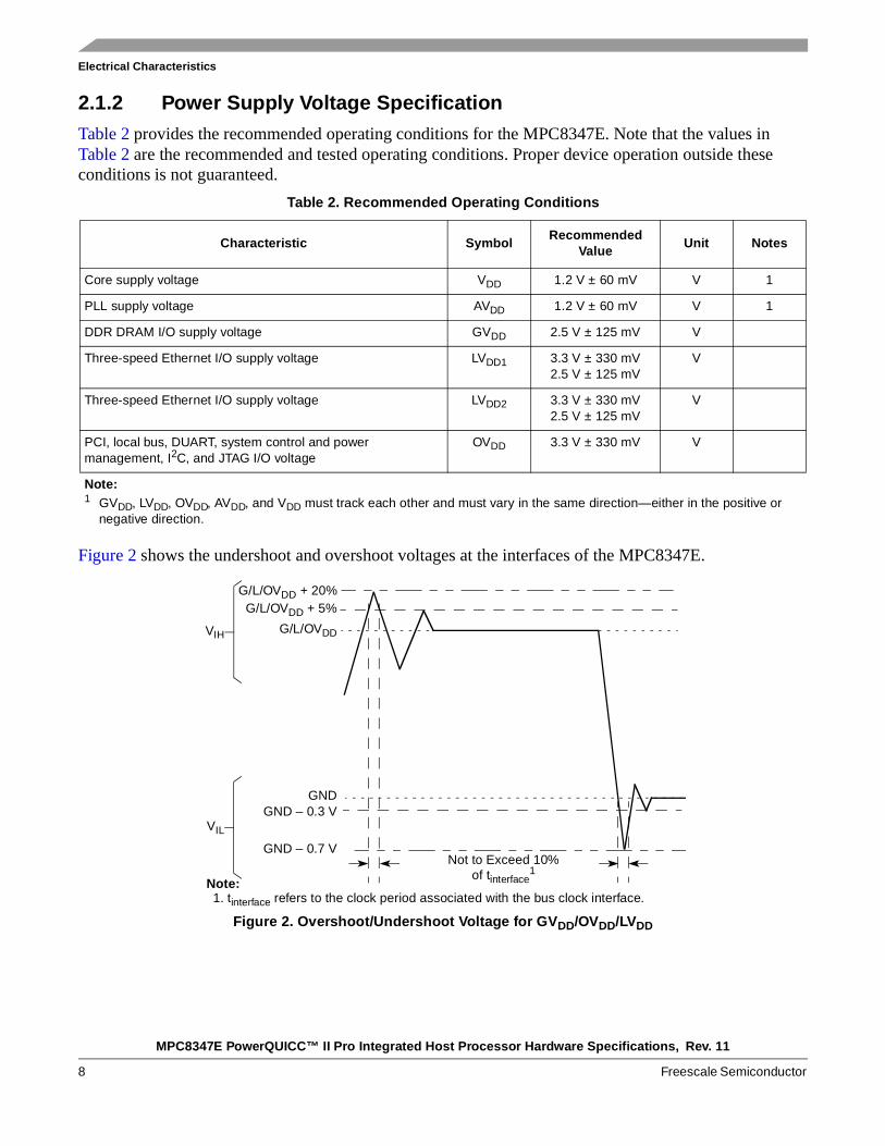
2.1.2 Power Supply Voltage SpecificationTable 2 provides the recommended operating conditions for the MPC8347E. Note that the values in Table 2 are the recommended and tested operating conditions. Proper device operation outside these conditions is not guaranteed.
Figure 2 shows the undershoot and overshoot voltages at the interfaces of the MPC8347E.
Figure 2. Overshoot/Undershoot Voltage for GVDD/OVDD/LVDD
Table 2. Recommended Operating Conditions
Characteristic SymbolRecommended
ValueUnit Notes
Core supply voltage VDD 1.2 V ± 60 mV V 1
PLL supply voltage AVDD 1.2 V ± 60 mV V 1
DDR DRAM I/O supply voltage GVDD 2.5 V ± 125 mV V
Three-speed Ethernet I/O supply voltage LVDD1 3.3 V ± 330 mV2.5 V ± 125 mV
V
Three-speed Ethernet I/O supply voltage LVDD2 3.3 V ± 330 mV2.5 V ± 125 mV
V
PCI, local bus, DUART, system control and power management, I2C, and JTAG I/O voltage
OVDD 3.3 V ± 330 mV V
Note: 1 GVDD, LVDD, OVDD, AVDD, and VDD must track each other and must vary in the same direction—either in the positive or
negative direction.
GNDGND – 0.3 V
GND – 0.7 VNot to Exceed 10%
G/L/OVDD + 20%
G/L/OVDD
G/L/OVDD + 5%
of tinterface1
1. tinterface refers to the clock period associated with the bus clock interface.
VIH
VIL
Note:
MPC8347E PowerQUICC™ II Pro Integrated Host Processor Hardware Specifications, Rev. 11
Freescale Semiconductor 9
Electrical Characteristics
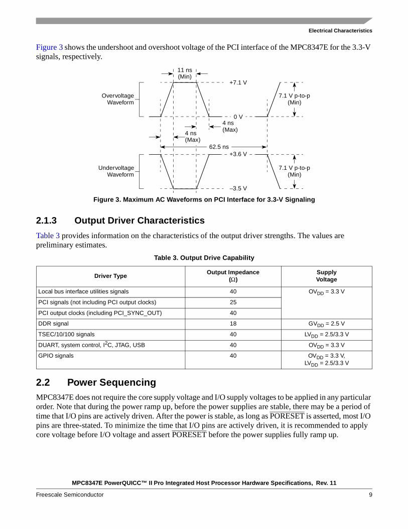
Figure 3 shows the undershoot and overshoot voltage of the PCI interface of the MPC8347E for the 3.3-V signals, respectively.
Figure 3. Maximum AC Waveforms on PCI Interface for 3.3-V Signaling
2.1.3 Output Driver Characteristics
Table 3 provides information on the characteristics of the output driver strengths. The values are preliminary estimates.
2.2 Power SequencingMPC8347E does not require the core supply voltage and I/O supply voltages to be applied in any particular order. Note that during the power ramp up, before the power supplies are stable, there may be a period of time that I/O pins are actively driven. After the power is stable, as long as PORESET is asserted, most I/O pins are three-stated. To minimize the time that I/O pins are actively driven, it is recommended to apply core voltage before I/O voltage and assert PORESET before the power supplies fully ramp up.
Table 3. Output Drive Capability
Driver TypeOutput Impedance
(Ω)SupplyVoltage
Local bus interface utilities signals 40 OVDD = 3.3 V
PCI signals (not including PCI output clocks) 25
PCI output clocks (including PCI_SYNC_OUT) 40
DDR signal 18 GVDD = 2.5 V
TSEC/10/100 signals 40 LVDD = 2.5/3.3 V
DUART, system control, I2C, JTAG, USB 40 OVDD = 3.3 V
GPIO signals 40 OVDD = 3.3 V,LVDD = 2.5/3.3 V
UndervoltageWaveform
OvervoltageWaveform
11 ns(Min)
+7.1 V
7.1 V p-to-p(Min)
4 ns(Max)
–3.5 V
7.1 V p-to-p(Min)
62.5 ns+3.6 V
0 V
4 ns(Max)
MPC8347E PowerQUICC™ II Pro Integrated Host Processor Hardware Specifications, Rev. 11
10 Freescale Semiconductor
Power Characteristics
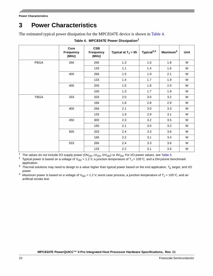
3 Power CharacteristicsThe estimated typical power dissipation for the MPC8347E device is shown in Table 4.
Table 4. MPC8347E Power Dissipation1
1 The values do not include I/O supply power (OVDD, LVDD, GVDD) or AVDD. For I/O power values, see Table 5.
Core Frequency
(MHz)
CSB Frequency
(MHz)Typical at TJ = 65 Typical2,3
2 Typical power is based on a voltage of VDD = 1.2 V, a junction temperature of TJ = 105°C, and a Dhrystone benchmark application.
3 Thermal solutions may need to design to a value higher than typical power based on the end application, TA target, and I/O power.
Maximum4
4 Maximum power is based on a voltage of VDD = 1.2 V, worst case process, a junction temperature of TJ = 105°C, and an artificial smoke test.
Unit
PBGA 266 266 1.3 1.6 1.8 W
133 1.1 1.4 1.6 W
400 266 1.5 1.9 2.1 W
133 1.4 1.7 1.9 W
400 200 1.5 1.8 2.0 W
100 1.3 1.7 1.9 W
TBGA 333 333 2.0 3.0 3.2 W
166 1.8 2.8 2.9 W
400 266 2.1 3.0 3.3 W
133 1.9 2.9 3.1 W
450 300 2.3 3.2 3.5 W
150 2.1 3.0 3.2 W
500 333 2.4 3.3 3.6 W
166 2.2 3.1 3.4 W
533 266 2.4 3.3 3.6 W
133 2.2 3.1 3.4 W
MPC8347E PowerQUICC™ II Pro Integrated Host Processor Hardware Specifications, Rev. 11
Freescale Semiconductor 11
Power Characteristics
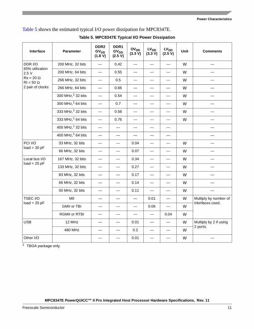
Table 5 shows the estimated typical I/O power dissipation for MPC8347E.
Table 5. MPC8347E Typical I/O Power Dissipation
Interface ParameterDDR2GVDD (1.8 V)
DDR1GVDD (2.5 V)
OVDD (3.3 V)
LVDD(3.3 V)
LVDD(2.5 V)
Unit Comments
DDR I/O65% utilization2.5 VRs = 20 ΩRt = 50 Ω2 pair of clocks
200 MHz, 32 bits — 0.42 — — — W —
200 MHz, 64 bits — 0.55 — — — W —
266 MHz, 32 bits — 0.5 — — — W —
266 MHz, 64 bits — 0.66 — — — W —
300 MHz,1 32 bits
1 TBGA package only.
— 0.54 — — — W —
300 MHz,1 64 bits — 0.7 — — — W —
333 MHz,1 32 bits — 0.58 — — — W —
333 MHz,1 64 bits — 0.76 — — — W —
400 MHz,1 32 bits — — — — — —
400 MHz,1 64 bits — — — — — —
PCI I/Oload = 30 pF
33 MHz, 32 bits — — 0.04 — — W —
66 MHz, 32 bits — — 0.07 — — W —
Local bus I/Oload = 25 pF
167 MHz, 32 bits — — 0.34 — — W —
133 MHz, 32 bits — — 0.27 — — W —
83 MHz, 32 bits — — 0.17 — — W —
66 MHz, 32 bits — — 0.14 — — W —
50 MHz, 32 bits — — 0.11 — — W —
TSEC I/Oload = 25 pF
MII — — — 0.01 — W Multiply by number of interfaces used.
GMII or TBI — — — 0.06 — W
RGMII or RTBI — — — — 0.04 W
USB 12 MHz — — 0.01 — — W Multiply by 2 if using 2 ports.
480 MHz — — 0.2 — — W
Other I/O — — 0.01 — — W —
MPC8347E PowerQUICC™ II Pro Integrated Host Processor Hardware Specifications, Rev. 11
12 Freescale Semiconductor
Clock Input Timing
4 Clock Input TimingThis section provides the clock input DC and AC electrical characteristics for the MPC8347E.
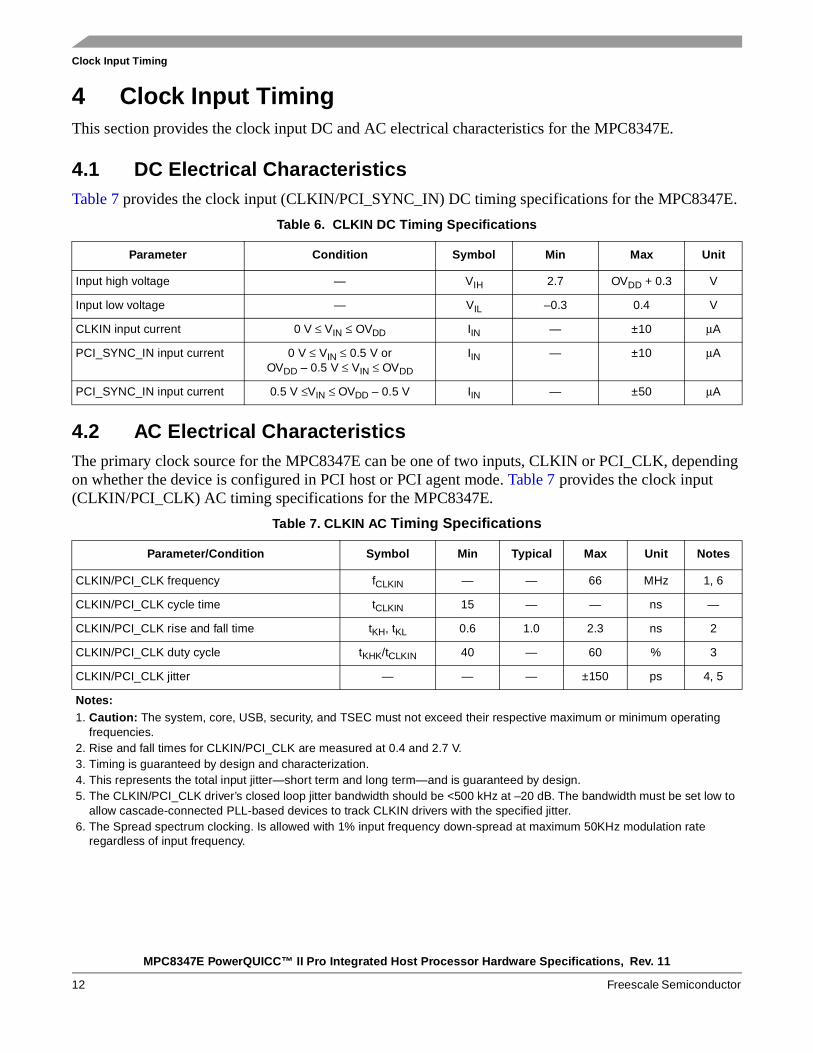
4.1 DC Electrical CharacteristicsTable 7 provides the clock input (CLKIN/PCI_SYNC_IN) DC timing specifications for the MPC8347E.
4.2 AC Electrical CharacteristicsThe primary clock source for the MPC8347E can be one of two inputs, CLKIN or PCI_CLK, depending on whether the device is configured in PCI host or PCI agent mode. Table 7 provides the clock input (CLKIN/PCI_CLK) AC timing specifications for the MPC8347E.
Table 6. CLKIN DC Timing Specifications
Parameter Condition Symbol Min Max Unit
Input high voltage — VIH 2.7 OVDD + 0.3 V
Input low voltage — VIL –0.3 0.4 V
CLKIN input current 0 V ≤ VIN ≤ OVDD IIN — ±10 μA
PCI_SYNC_IN input current 0 V ≤ VIN ≤ 0.5 V or OVDD – 0.5 V ≤ VIN ≤ OVDD
IIN — ±10 μA
PCI_SYNC_IN input current 0.5 V ≤VIN ≤ OVDD – 0.5 V IIN — ±50 μA
Table 7. CLKIN AC Timing Specifications
Parameter/Condition Symbol Min Typical Max Unit Notes
CLKIN/PCI_CLK frequency fCLKIN — — 66 MHz 1, 6
CLKIN/PCI_CLK cycle time tCLKIN 15 — — ns —
CLKIN/PCI_CLK rise and fall time tKH, tKL 0.6 1.0 2.3 ns 2
CLKIN/PCI_CLK duty cycle tKHK/tCLKIN 40 — 60 % 3
CLKIN/PCI_CLK jitter — — — ±150 ps 4, 5
Notes:1. Caution: The system, core, USB, security, and TSEC must not exceed their respective maximum or minimum operating
frequencies. 2. Rise and fall times for CLKIN/PCI_CLK are measured at 0.4 and 2.7 V.3. Timing is guaranteed by design and characterization.4. This represents the total input jitter—short term and long term—and is guaranteed by design.5. The CLKIN/PCI_CLK driver’s closed loop jitter bandwidth should be <500 kHz at –20 dB. The bandwidth must be set low to
allow cascade-connected PLL-based devices to track CLKIN drivers with the specified jitter.6. The Spread spectrum clocking. Is allowed with 1% input frequency down-spread at maximum 50KHz modulation rate
regardless of input frequency.
MPC8347E PowerQUICC™ II Pro Integrated Host Processor Hardware Specifications, Rev. 11
Freescale Semiconductor 13
RESET Initialization
5 RESET InitializationThis section describes the DC and AC electrical specifications for the reset initialization timing and electrical requirements of the MPC8347E.
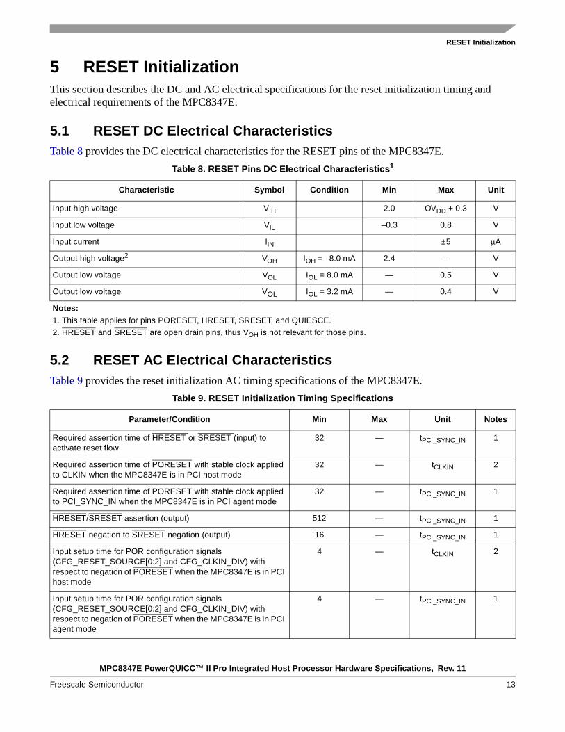
5.1 RESET DC Electrical CharacteristicsTable 8 provides the DC electrical characteristics for the RESET pins of the MPC8347E.
5.2 RESET AC Electrical CharacteristicsTable 9 provides the reset initialization AC timing specifications of the MPC8347E.
Table 8. RESET Pins DC Electrical Characteristics1
Characteristic Symbol Condition Min Max Unit
Input high voltage VIH 2.0 OVDD + 0.3 V
Input low voltage VIL –0.3 0.8 V
Input current IIN ±5 μA
Output high voltage2 VOH IOH = –8.0 mA 2.4 — V
Output low voltage VOL IOL = 8.0 mA — 0.5 V
Output low voltage VOL IOL = 3.2 mA — 0.4 V
Notes:1. This table applies for pins PORESET, HRESET, SRESET, and QUIESCE.
2. HRESET and SRESET are open drain pins, thus VOH is not relevant for those pins.
Table 9. RESET Initialization Timing Specifications
Parameter/Condition Min Max Unit Notes
Required assertion time of HRESET or SRESET (input) to activate reset flow
32 — tPCI_SYNC_IN 1
Required assertion time of PORESET with stable clock applied to CLKIN when the MPC8347E is in PCI host mode
32 — tCLKIN 2
Required assertion time of PORESET with stable clock applied to PCI_SYNC_IN when the MPC8347E is in PCI agent mode
32 — tPCI_SYNC_IN 1
HRESET/SRESET assertion (output) 512 — tPCI_SYNC_IN 1
HRESET negation to SRESET negation (output) 16 — tPCI_SYNC_IN 1
Input setup time for POR configuration signals (CFG_RESET_SOURCE[0:2] and CFG_CLKIN_DIV) with respect to negation of PORESET when the MPC8347E is in PCI host mode
4 — tCLKIN 2
Input setup time for POR configuration signals (CFG_RESET_SOURCE[0:2] and CFG_CLKIN_DIV) with respect to negation of PORESET when the MPC8347E is in PCI agent mode
4 — tPCI_SYNC_IN 1
MPC8347E PowerQUICC™ II Pro Integrated Host Processor Hardware Specifications, Rev. 11
14 Freescale Semiconductor
RESET Initialization
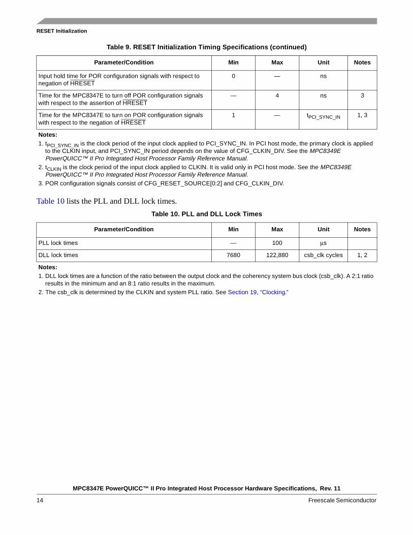
Table 10 lists the PLL and DLL lock times.
Input hold time for POR configuration signals with respect to negation of HRESET
0 — ns
Time for the MPC8347E to turn off POR configuration signals with respect to the assertion of HRESET
— 4 ns 3
Time for the MPC8347E to turn on POR configuration signals with respect to the negation of HRESET
1 — tPCI_SYNC_IN 1, 3
Notes:1. tPCI_SYNC_IN is the clock period of the input clock applied to PCI_SYNC_IN. In PCI host mode, the primary clock is applied
to the CLKIN input, and PCI_SYNC_IN period depends on the value of CFG_CLKIN_DIV. See the MPC8349E PowerQUICC™ II Pro Integrated Host Processor Family Reference Manual.
2. tCLKIN is the clock period of the input clock applied to CLKIN. It is valid only in PCI host mode. See the MPC8349E PowerQUICC™ II Pro Integrated Host Processor Family Reference Manual.
3. POR configuration signals consist of CFG_RESET_SOURCE[0:2] and CFG_CLKIN_DIV.
Table 10. PLL and DLL Lock Times
Parameter/Condition Min Max Unit Notes
PLL lock times — 100 μs
DLL lock times 7680 122,880 csb_clk cycles 1, 2
Notes:1. DLL lock times are a function of the ratio between the output clock and the coherency system bus clock (csb_clk). A 2:1 ratio
results in the minimum and an 8:1 ratio results in the maximum.
2. The csb_clk is determined by the CLKIN and system PLL ratio. See Section 19, “Clocking.”
Table 9. RESET Initialization Timing Specifications (continued)
Parameter/Condition Min Max Unit Notes
MPC8347E PowerQUICC™ II Pro Integrated Host Processor Hardware Specifications, Rev. 11
Freescale Semiconductor 15
DDR SDRAM
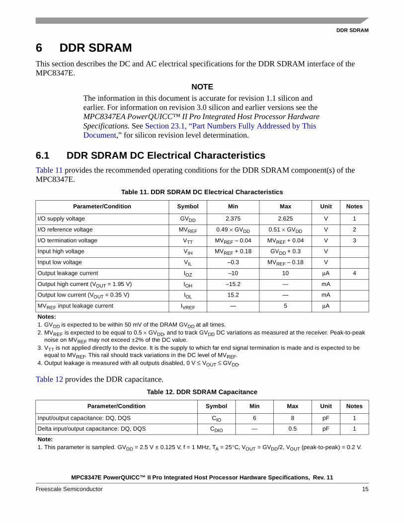
6 DDR SDRAMThis section describes the DC and AC electrical specifications for the DDR SDRAM interface of the MPC8347E.
NOTEThe information in this document is accurate for revision 1.1 silicon and earlier. For information on revision 3.0 silicon and earlier versions see the MPC8347EA PowerQUICC™ II Pro Integrated Host Processor Hardware Specifications. See Section 23.1, “Part Numbers Fully Addressed by This Document,” for silicon revision level determination.
6.1 DDR SDRAM DC Electrical CharacteristicsTable 11 provides the recommended operating conditions for the DDR SDRAM component(s) of the MPC8347E.
Table 12 provides the DDR capacitance.
Table 11. DDR SDRAM DC Electrical Characteristics
Parameter/Condition Symbol Min Max Unit Notes
I/O supply voltage GVDD 2.375 2.625 V 1
I/O reference voltage MVREF 0.49 × GVDD 0.51 × GVDD V 2
I/O termination voltage VTT MVREF – 0.04 MVREF + 0.04 V 3
Input high voltage VIH MVREF + 0.18 GVDD + 0.3 V
Input low voltage VIL –0.3 MVREF – 0.18 V
Output leakage current IOZ –10 10 μA 4
Output high current (VOUT = 1.95 V) IOH –15.2 — mA
Output low current (VOUT = 0.35 V) IOL 15.2 — mA
MVREF input leakage current IVREF — 5 μA
Notes:1. GVDD is expected to be within 50 mV of the DRAM GVDD at all times.2. MVREF is expected to be equal to 0.5 × GVDD, and to track GVDD DC variations as measured at the receiver. Peak-to-peak
noise on MVREF may not exceed ±2% of the DC value.3. VTT is not applied directly to the device. It is the supply to which far end signal termination is made and is expected to be
equal to MVREF. This rail should track variations in the DC level of MVREF.4. Output leakage is measured with all outputs disabled, 0 V ≤ VOUT ≤ GVDD.
Table 12. DDR SDRAM Capacitance
Parameter/Condition Symbol Min Max Unit Notes
Input/output capacitance: DQ, DQS CIO 6 8 pF 1
Delta input/output capacitance: DQ, DQS CDIO — 0.5 pF 1
Note:1. This parameter is sampled. GVDD = 2.5 V ± 0.125 V, f = 1 MHz, TA = 25°C, VOUT = GVDD/2, VOUT (peak-to-peak) = 0.2 V.
MPC8347E PowerQUICC™ II Pro Integrated Host Processor Hardware Specifications, Rev. 11
16 Freescale Semiconductor
DDR SDRAM
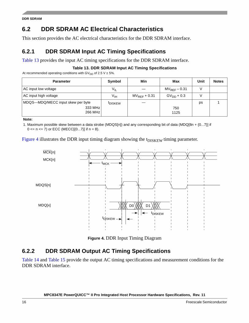
6.2 DDR SDRAM AC Electrical CharacteristicsThis section provides the AC electrical characteristics for the DDR SDRAM interface.
6.2.1 DDR SDRAM Input AC Timing SpecificationsTable 13 provides the input AC timing specifications for the DDR SDRAM interface.
Figure 4 illustrates the DDR input timing diagram showing the tDISKEW timing parameter.
Figure 4. DDR Input Timing Diagram
6.2.2 DDR SDRAM Output AC Timing SpecificationsTable 14 and Table 15 provide the output AC timing specifications and measurement conditions for the DDR SDRAM interface.
Table 13. DDR SDRAM Input AC Timing SpecificationsAt recommended operating conditions with GVDD of 2.5 V ± 5%.
Parameter Symbol Min Max Unit Notes
AC input low voltage VIL — MVREF – 0.31 V
AC input high voltage VIH MVREF + 0.31 GVDD + 0.3 V
MDQS—MDQ/MECC input skew per byte
333 MHz266 MHz
tDISKEW —
7501125
ps 1
Note:1. Maximum possible skew between a data strobe (MDQS[n]) and any corresponding bit of data (MDQ[8n + {0...7}] if
0 <= n <= 7) or ECC (MECC[{0...7}] if n = 8).
MCK[n]
MCK[n]tMCK
MDQ[x]
MDQS[n]
tDISKEW
D1D0
tDISKEW
MPC8347E PowerQUICC™ II Pro Integrated Host Processor Hardware Specifications, Rev. 11
Freescale Semiconductor 17
DDR SDRAM
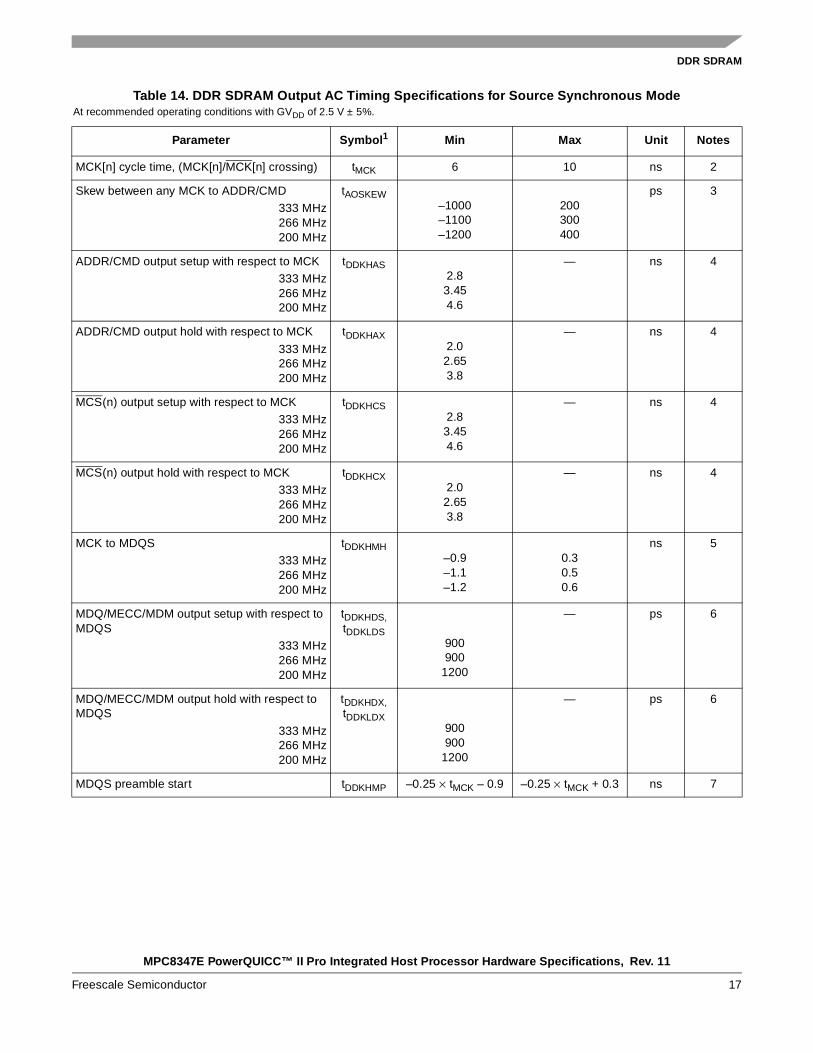
Table 14. DDR SDRAM Output AC Timing Specifications for Source Synchronous ModeAt recommended operating conditions with GVDD of 2.5 V ± 5%.
Parameter Symbol1 Min Max Unit Notes
MCK[n] cycle time, (MCK[n]/MCK[n] crossing) tMCK 6 10 ns 2
Skew between any MCK to ADDR/CMD
333 MHz266 MHz200 MHz
tAOSKEW–1000–1100–1200
200300400
ps 3
ADDR/CMD output setup with respect to MCK
333 MHz266 MHz200 MHz
tDDKHAS2.83.454.6
— ns 4
ADDR/CMD output hold with respect to MCK
333 MHz266 MHz200 MHz
tDDKHAX2.0 2.653.8
— ns 4
MCS(n) output setup with respect to MCK
333 MHz266 MHz200 MHz
tDDKHCS2.83.454.6
— ns 4
MCS(n) output hold with respect to MCK
333 MHz266 MHz200 MHz
tDDKHCX2.02.653.8
— ns 4
MCK to MDQS
333 MHz266 MHz200 MHz
tDDKHMH–0.9–1.1–1.2
0.30.50.6
ns 5
MDQ/MECC/MDM output setup with respect to MDQS
333 MHz266 MHz200 MHz
tDDKHDS,tDDKLDS
900900
1200
— ps 6
MDQ/MECC/MDM output hold with respect to MDQS
333 MHz266 MHz200 MHz
tDDKHDX,tDDKLDX
900900
1200
— ps 6
MDQS preamble start tDDKHMP –0.25 × tMCK – 0.9 –0.25 × tMCK + 0.3 ns 7
MPC8347E PowerQUICC™ II Pro Integrated Host Processor Hardware Specifications, Rev. 11
18 Freescale Semiconductor
DDR SDRAM
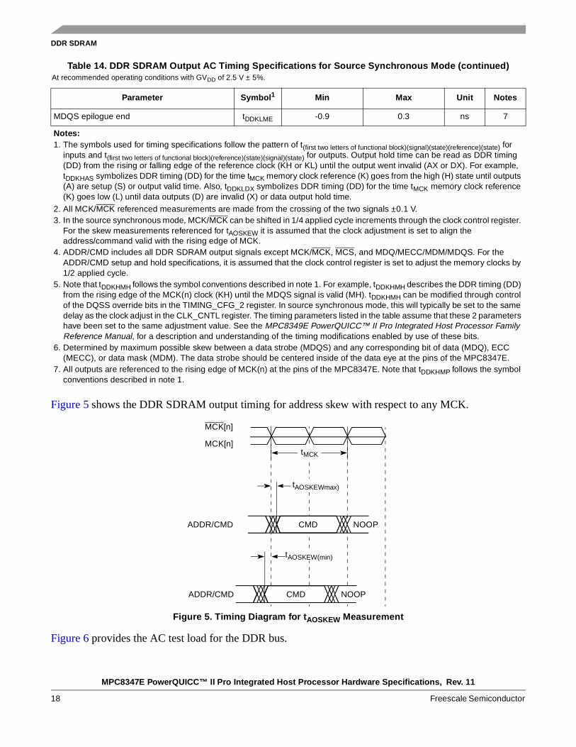
Figure 5 shows the DDR SDRAM output timing for address skew with respect to any MCK.
Figure 5. Timing Diagram for tAOSKEW Measurement
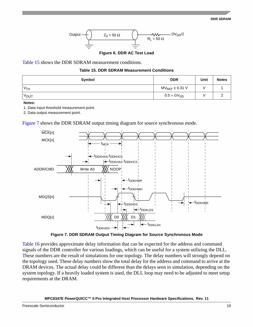
Figure 6 provides the AC test load for the DDR bus.
MDQS epilogue end tDDKLME -0.9 0.3 ns 7
Notes:1. The symbols used for timing specifications follow the pattern of t(first two letters of functional block)(signal)(state)(reference)(state) for
inputs and t(first two letters of functional block)(reference)(state)(signal)(state) for outputs. Output hold time can be read as DDR timing (DD) from the rising or falling edge of the reference clock (KH or KL) until the output went invalid (AX or DX). For example, tDDKHAS symbolizes DDR timing (DD) for the time tMCK memory clock reference (K) goes from the high (H) state until outputs (A) are setup (S) or output valid time. Also, tDDKLDX symbolizes DDR timing (DD) for the time tMCK memory clock reference (K) goes low (L) until data outputs (D) are invalid (X) or data output hold time.
2. All MCK/MCK referenced measurements are made from the crossing of the two signals ±0.1 V.3. In the source synchronous mode, MCK/MCK can be shifted in 1/4 applied cycle increments through the clock control register.
For the skew measurements referenced for tAOSKEW it is assumed that the clock adjustment is set to align the address/command valid with the rising edge of MCK.
4. ADDR/CMD includes all DDR SDRAM output signals except MCK/MCK, MCS, and MDQ/MECC/MDM/MDQS. For the ADDR/CMD setup and hold specifications, it is assumed that the clock control register is set to adjust the memory clocks by 1/2 applied cycle.
5. Note that tDDKHMH follows the symbol conventions described in note 1. For example, tDDKHMH describes the DDR timing (DD) from the rising edge of the MCK(n) clock (KH) until the MDQS signal is valid (MH). tDDKHMH can be modified through control of the DQSS override bits in the TIMING_CFG_2 register. In source synchronous mode, this will typically be set to the same delay as the clock adjust in the CLK_CNTL register. The timing parameters listed in the table assume that these 2 parameters have been set to the same adjustment value. See the MPC8349E PowerQUICC™ II Pro Integrated Host Processor Family Reference Manual, for a description and understanding of the timing modifications enabled by use of these bits.
6. Determined by maximum possible skew between a data strobe (MDQS) and any corresponding bit of data (MDQ), ECC (MECC), or data mask (MDM). The data strobe should be centered inside of the data eye at the pins of the MPC8347E.
7. All outputs are referenced to the rising edge of MCK(n) at the pins of the MPC8347E. Note that tDDKHMP follows the symbol conventions described in note 1.
Table 14. DDR SDRAM Output AC Timing Specifications for Source Synchronous Mode (continued)At recommended operating conditions with GVDD of 2.5 V ± 5%.
Parameter Symbol1 Min Max Unit Notes
ADDR/CMD
MCK[n]
MCK[n]tMCK
CMD NOOP
ADDR/CMD CMD NOOP
tAOSKEWmax)
tAOSKEW(min)
MPC8347E PowerQUICC™ II Pro Integrated Host Processor Hardware Specifications, Rev. 11
Freescale Semiconductor 19
DDR SDRAM
Figure 6. DDR AC Test Load
Table 15 shows the DDR SDRAM measurement conditions.
Figure 7 shows the DDR SDRAM output timing diagram for source synchronous mode.
Figure 7. DDR SDRAM Output Timing Diagram for Source Synchronous Mode
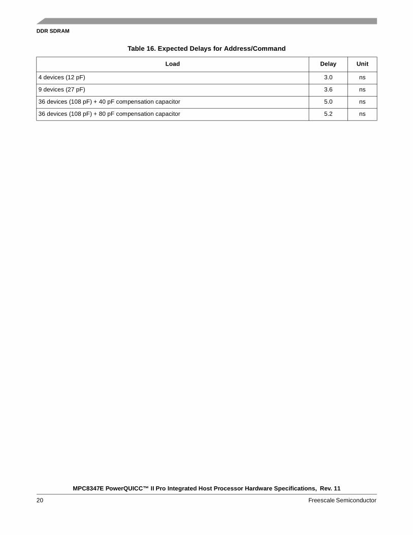
Table 16 provides approximate delay information that can be expected for the address and command signals of the DDR controller for various loadings, which can be useful for a system utilizing the DLL. These numbers are the result of simulations for one topology. The delay numbers will strongly depend on the topology used. These delay numbers show the total delay for the address and command to arrive at the DRAM devices. The actual delay could be different than the delays seen in simulation, depending on the system topology. If a heavily loaded system is used, the DLL loop may need to be adjusted to meet setup requirements at the DRAM.
Table 15. DDR SDRAM Measurement Conditions
Symbol DDR Unit Notes
VTH MVREF ± 0.31 V V 1
VOUT 0.5 × GVDD V 2
Notes:1. Data input threshold measurement point.2. Data output measurement point.
Output Z0 = 50 Ω OVDD/2RL = 50 Ω
ADDR/CMD
tDDKLDS
tDDKHDS
MDQ[x]
MDQS[n]
MCK[n]
MCK[n]tMCK
tDDKLDXtDDKHDX
D1D0
tDDKHAX,tDDKHCX
Write A0 NOOP
tDDKHAS,tDDKHCS
tDDKHMH
tDDKHME
tDDKHMP
MPC8347E PowerQUICC™ II Pro Integrated Host Processor Hardware Specifications, Rev. 11
20 Freescale Semiconductor
DDR SDRAM
Table 16. Expected Delays for Address/Command
Load Delay Unit
4 devices (12 pF) 3.0 ns
9 devices (27 pF) 3.6 ns
36 devices (108 pF) + 40 pF compensation capacitor 5.0 ns
36 devices (108 pF) + 80 pF compensation capacitor 5.2 ns
MPC8347E PowerQUICC™ II Pro Integrated Host Processor Hardware Specifications, Rev. 11
Freescale Semiconductor 21
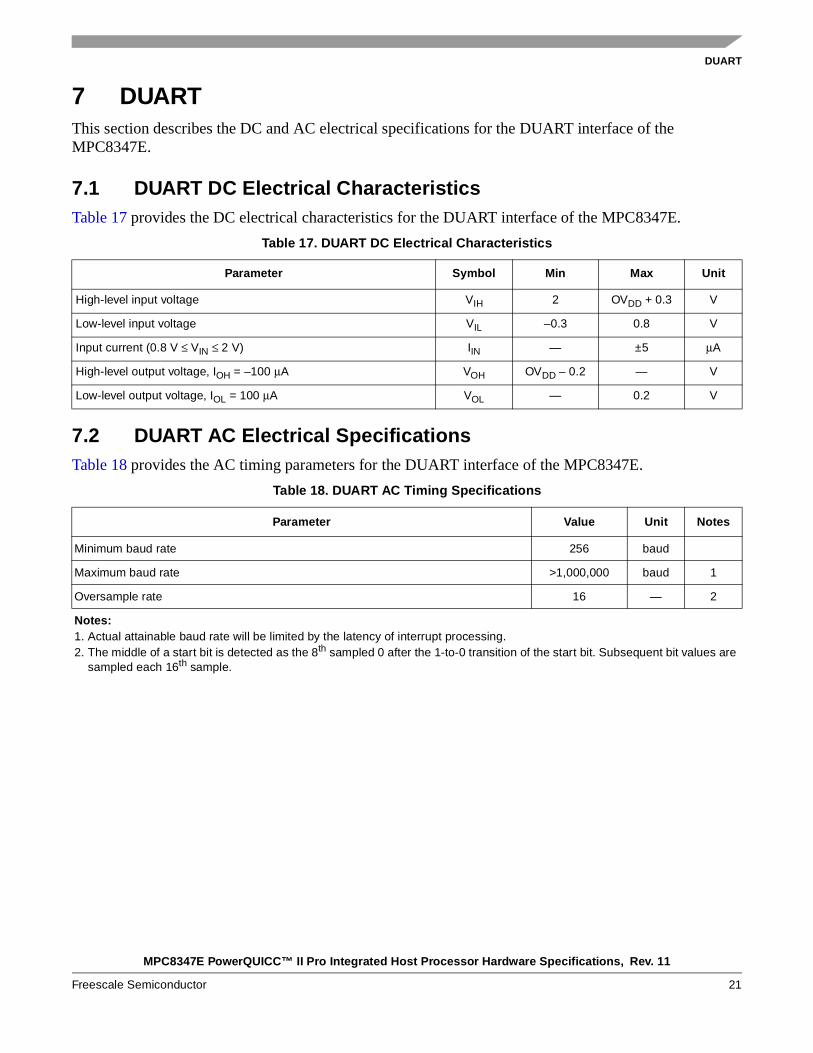
DUART
7 DUARTThis section describes the DC and AC electrical specifications for the DUART interface of the MPC8347E.
7.1 DUART DC Electrical Characteristics Table 17 provides the DC electrical characteristics for the DUART interface of the MPC8347E.
7.2 DUART AC Electrical SpecificationsTable 18 provides the AC timing parameters for the DUART interface of the MPC8347E.
Table 17. DUART DC Electrical Characteristics
Parameter Symbol Min Max Unit
High-level input voltage VIH 2 OVDD + 0.3 V
Low-level input voltage VIL –0.3 0.8 V
Input current (0.8 V ≤ VIN ≤ 2 V) IIN — ±5 μA
High-level output voltage, IOH = –100 μA VOH OVDD – 0.2 — V
Low-level output voltage, IOL = 100 μA VOL — 0.2 V
Table 18. DUART AC Timing Specifications
Parameter Value Unit Notes
Minimum baud rate 256 baud
Maximum baud rate >1,000,000 baud 1
Oversample rate 16 — 2
Notes:1. Actual attainable baud rate will be limited by the latency of interrupt processing.2. The middle of a start bit is detected as the 8th sampled 0 after the 1-to-0 transition of the start bit. Subsequent bit values are
sampled each 16th sample.
MPC8347E PowerQUICC™ II Pro Integrated Host Processor Hardware Specifications, Rev. 11
22 Freescale Semiconductor
Ethernet: Three-Speed Ethernet, MII Management
8 Ethernet: Three-Speed Ethernet, MII ManagementThis section provides the AC and DC electrical characteristics for three-speeds (10/100/1000 Mbps) and MII management.
8.1 Three-Speed Ethernet Controller (TSEC)— GMII/MII/TBI/RGMII/RTBI Electrical Characteristics
The electrical characteristics specified here apply to the gigabit media independent interface (GMII), the media independent interface (MII), ten-bit interface (TBI), reduced gigabit media independent interface (RGMII), and reduced ten-bit interface (RTBI) signals except management data input/output (MDIO) and management data clock (MDC). The MII, GMII, and TBI interfaces are defined for 3.3 V, and the RGMII and RTBI interfaces are defined for 2.5 V. The RGMII and RTBI interfaces follow the Hewlett-Packard Reduced Pin-Count Interface for Gigabit Ethernet Physical Layer Device Specification, Version 1.2a (9/22/2000). The electrical characteristics for MDIO and MDC are specified in Section 8.3, “Ethernet Management Interface Electrical Characteristics.”
8.1.1 TSEC DC Electrical CharacteristicsGMII, MII, TBI, RGMII, and RTBI drivers and receivers comply with the DC parametric attributes specified in Table 19 and Table 20. The RGMII and RTBI signals in Table 20 are based on a 2.5-V CMOS interface voltage as defined by JEDEC EIA/JESD8-5.
Table 19. GMII/TBI and MII DC Electrical Characteristics
Parameter Symbol Conditions Min Max Unit
Supply voltage 3.3 V LVDD2 — 2.97 3.63 V
Output high voltage VOH IOH = –4.0 mA LVDD = Min 2.40 LVDD + 0.3 V
Output low voltage VOL IOL = 4.0 mA LVDD = Min GND 0.50 V
Input high voltage VIH — — 2.0 LVDD + 0.3 V
Input low voltage VIL — — –0.3 0.90 V
Input high current IIH VIN1 = LVDD — 40 μA
Input low current IIL VIN1 = GND –600 — μA
Notes:1. The symbol VIN, in this case, represents the LVIN symbol referenced in Table 1 and Table 2.2. GMII/MII pins not needed for RGMII or RTBI operation are powered by the OVDD supply.
MPC8347E PowerQUICC™ II Pro Integrated Host Processor Hardware Specifications, Rev. 11
Freescale Semiconductor 23
Ethernet: Three-Speed Ethernet, MII Management
8.2 GMII, MII, TBI, RGMII, and RTBI AC Timing SpecificationsThe AC timing specifications for GMII, MII, TBI, RGMII, and RTBI are presented in this section.
8.2.1 GMII Timing SpecificationsThis section describes the GMII transmit and receive AC timing specifications.
8.2.1.1 GMII Transmit AC Timing Specifications
Table 21 provides the GMII transmit AC timing specifications.
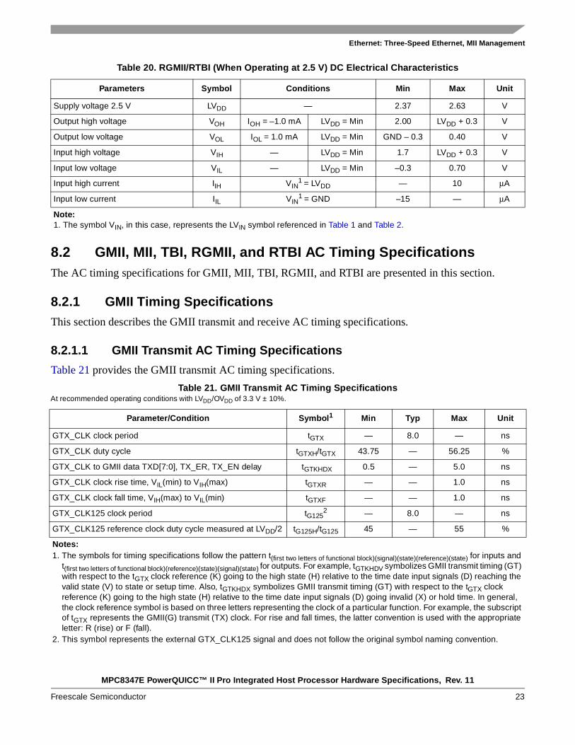
Table 20. RGMII/RTBI (When Operating at 2.5 V) DC Electrical Characteristics
Parameters Symbol Conditions Min Max Unit
Supply voltage 2.5 V LVDD — 2.37 2.63 V
Output high voltage VOH IOH = –1.0 mA LVDD = Min 2.00 LVDD + 0.3 V
Output low voltage VOL IOL = 1.0 mA LVDD = Min GND – 0.3 0.40 V
Input high voltage VIH — LVDD = Min 1.7 LVDD + 0.3 V
Input low voltage VIL — LVDD = Min –0.3 0.70 V
Input high current IIH VIN1 = LVDD — 10 μA
Input low current IIL VIN1 = GND –15 — μA
Note:1. The symbol VIN, in this case, represents the LVIN symbol referenced in Table 1 and Table 2.
Table 21. GMII Transmit AC Timing SpecificationsAt recommended operating conditions with LVDD/OVDD of 3.3 V ± 10%.
Parameter/Condition Symbol1 Min Typ Max Unit
GTX_CLK clock period tGTX — 8.0 — ns
GTX_CLK duty cycle tGTXH/tGTX 43.75 — 56.25 %
GTX_CLK to GMII data TXD[7:0], TX_ER, TX_EN delay tGTKHDX 0.5 — 5.0 ns
GTX_CLK clock rise time, VIL(min) to VIH(max) tGTXR — — 1.0 ns
GTX_CLK clock fall time, VIH(max) to VIL(min) tGTXF — — 1.0 ns
GTX_CLK125 clock period tG1252 — 8.0 — ns
GTX_CLK125 reference clock duty cycle measured at LVDD/2 tG125H/tG125 45 — 55 %
Notes:1. The symbols for timing specifications follow the pattern t(first two letters of functional block)(signal)(state)(reference)(state) for inputs and
t(first two letters of functional block)(reference)(state)(signal)(state) for outputs. For example, tGTKHDV symbolizes GMII transmit timing (GT) with respect to the tGTX clock reference (K) going to the high state (H) relative to the time date input signals (D) reaching the valid state (V) to state or setup time. Also, tGTKHDX symbolizes GMII transmit timing (GT) with respect to the tGTX clock reference (K) going to the high state (H) relative to the time date input signals (D) going invalid (X) or hold time. In general, the clock reference symbol is based on three letters representing the clock of a particular function. For example, the subscript of tGTX represents the GMII(G) transmit (TX) clock. For rise and fall times, the latter convention is used with the appropriate letter: R (rise) or F (fall).
2. This symbol represents the external GTX_CLK125 signal and does not follow the original symbol naming convention.
MPC8347E PowerQUICC™ II Pro Integrated Host Processor Hardware Specifications, Rev. 11
24 Freescale Semiconductor
Ethernet: Three-Speed Ethernet, MII Management
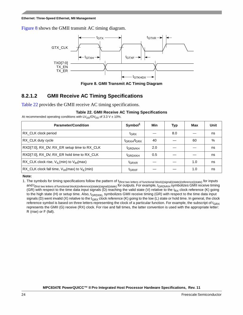
Figure 8 shows the GMII transmit AC timing diagram.
Figure 8. GMII Transmit AC Timing Diagram
8.2.1.2 GMII Receive AC Timing Specifications
Table 22 provides the GMII receive AC timing specifications.
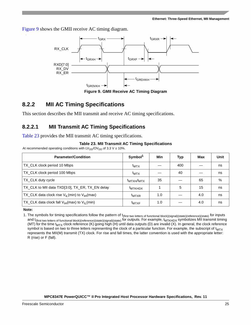
Table 22. GMII Receive AC Timing SpecificationsAt recommended operating conditions with LVDD/OVDD of 3.3 V ± 10%.
Parameter/Condition Symbol1 Min Typ Max Unit
RX_CLK clock period tGRX — 8.0 — ns
RX_CLK duty cycle tGRXH/tGRX 40 — 60 %
RXD[7:0], RX_DV, RX_ER setup time to RX_CLK tGRDVKH 2.0 — — ns
RXD[7:0], RX_DV, RX_ER hold time to RX_CLK tGRDXKH 0.5 — — ns
RX_CLK clock rise, VIL(min) to VIH(max) tGRXR — — 1.0 ns
RX_CLK clock fall time, VIH(max) to VIL(min) tGRXF — — 1.0 ns
Note:1. The symbols for timing specifications follow the pattern of t(first two letters of functional block)(signal)(state)(reference)(state) for inputs
and t(first two letters of functional block)(reference)(state)(signal)(state) for outputs. For example, tGRDVKH symbolizes GMII receive timing (GR) with respect to the time data input signals (D) reaching the valid state (V) relative to the tRX clock reference (K) going to the high state (H) or setup time. Also, tGRDXKL symbolizes GMII receive timing (GR) with respect to the time data input signals (D) went invalid (X) relative to the tGRX clock reference (K) going to the low (L) state or hold time. In general, the clock reference symbol is based on three letters representing the clock of a particular function. For example, the subscript of tGRX represents the GMII (G) receive (RX) clock. For rise and fall times, the latter convention is used with the appropriate letter: R (rise) or F (fall).
GTX_CLK
TXD[7:0]
tGTKHDX
tGTX
tGTXH
tGTXR
tGTXF
TX_ENTX_ER
MPC8347E PowerQUICC™ II Pro Integrated Host Processor Hardware Specifications, Rev. 11
Freescale Semiconductor 25
Ethernet: Three-Speed Ethernet, MII Management
Figure 9 shows the GMII receive AC timing diagram.G
Figure 9. GMII Receive AC Timing Diagram
8.2.2 MII AC Timing Specifications
This section describes the MII transmit and receive AC timing specifications.
8.2.2.1 MII Transmit AC Timing Specifications
Table 23 provides the MII transmit AC timing specifications.
Table 23. MII Transmit AC Timing SpecificationsAt recommended operating conditions with LVDD/OVDD of 3.3 V ± 10%.
Parameter/Condition Symbol1 Min Typ Max Unit
TX_CLK clock period 10 Mbps tMTX — 400 — ns
TX_CLK clock period 100 Mbps tMTX — 40 — ns
TX_CLK duty cycle tMTXH/tMTX 35 — 65 %
TX_CLK to MII data TXD[3:0], TX_ER, TX_EN delay tMTKHDX 1 5 15 ns
TX_CLK data clock rise VIL(min) to VIH(max) tMTXR 1.0 — 4.0 ns
TX_CLK data clock fall VIH(max) to VIL(min) tMTXF 1.0 — 4.0 ns
Note:1. The symbols for timing specifications follow the pattern of t(first two letters of functional block)(signal)(state)(reference)(state) for inputs
and t(first two letters of functional block)(reference)(state)(signal)(state) for outputs. For example, tMTKHDX symbolizes MII transmit timing (MT) for the time tMTX clock reference (K) going high (H) until data outputs (D) are invalid (X). In general, the clock reference symbol is based on two to three letters representing the clock of a particular function. For example, the subscript of tMTX represents the MII(M) transmit (TX) clock. For rise and fall times, the latter convention is used with the appropriate letter: R (rise) or F (fall).
RX_CLK
RXD[7:0]
tGRDXKH
tGRX
tGRXH
tGRXR
tGRXF
tGRDVKH
RX_DVRX_ER
MPC8347E PowerQUICC™ II Pro Integrated Host Processor Hardware Specifications, Rev. 11
26 Freescale Semiconductor
Ethernet: Three-Speed Ethernet, MII Management
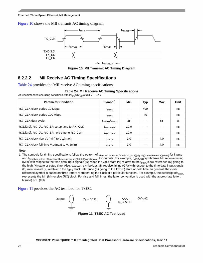
Figure 10 shows the MII transmit AC timing diagram.
Figure 10. MII Transmit AC Timing Diagram
8.2.2.2 MII Receive AC Timing Specifications
Table 24 provides the MII receive AC timing specifications.
Figure 11 provides the AC test load for TSEC.
Figure 11. TSEC AC Test Load
Table 24. MII Receive AC Timing SpecificationsAt recommended operating conditions with LVDD/OVDD of 3.3 V ± 10%.
Parameter/Condition Symbol1 Min Typ Max Unit
RX_CLK clock period 10 Mbps tMRX — 400 — ns
RX_CLK clock period 100 Mbps tMRX — 40 — ns
RX_CLK duty cycle tMRXH/tMRX 35 — 65 %
RXD[3:0], RX_DV, RX_ER setup time to RX_CLK tMRDVKH 10.0 — — ns
RXD[3:0], RX_DV, RX_ER hold time to RX_CLK tMRDXKH 10.0 — — ns
RX_CLK clock rise VIL(min) to VIH(max) tMRXR 1.0 — 4.0 ns
RX_CLK clock fall time VIH(max) to VIL(min) tMRXF 1.0 — 4.0 ns
Note:1. The symbols for timing specifications follow the pattern of t(first two letters of functional block)(signal)(state)(reference)(state) for inputs
and t(first two letters of functional block)(reference)(state)(signal)(state) for outputs. For example, tMRDVKH symbolizes MII receive timing (MR) with respect to the time data input signals (D) reach the valid state (V) relative to the tMRX clock reference (K) going to the high (H) state or setup time. Also, tMRDXKL symbolizes MII receive timing (GR) with respect to the time data input signals (D) went invalid (X) relative to the tMRX clock reference (K) going to the low (L) state or hold time. In general, the clock reference symbol is based on three letters representing the clock of a particular functionl. For example, the subscript of tMRX represents the MII (M) receive (RX) clock. For rise and fall times, the latter convention is used with the appropriate letter: R (rise) or F (fall).
TX_CLK
TXD[3:0]
tMTKHDX
tMTX
tMTXH
tMTXR
tMTXF
TX_ENTX_ER
Output Z0 = 50 Ω OVDD/2RL = 50 Ω
MPC8347E PowerQUICC™ II Pro Integrated Host Processor Hardware Specifications, Rev. 11
Freescale Semiconductor 27
Ethernet: Three-Speed Ethernet, MII Management
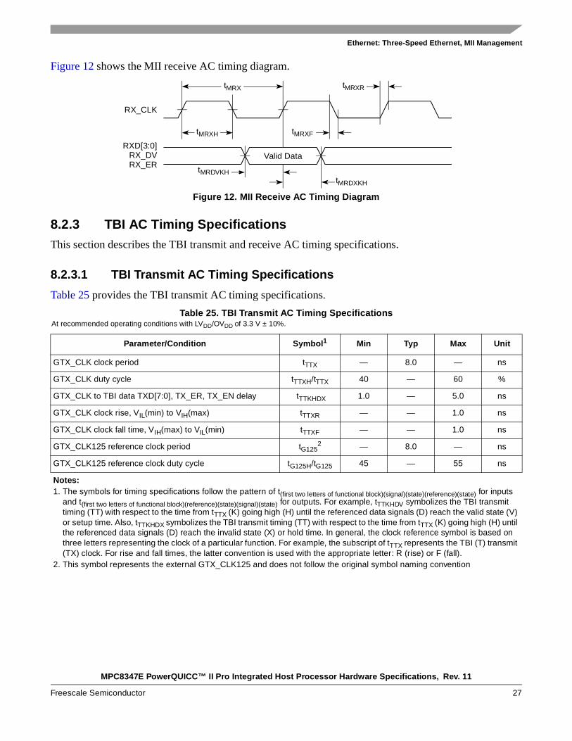
Figure 12 shows the MII receive AC timing diagram.
Figure 12. MII Receive AC Timing Diagram
8.2.3 TBI AC Timing SpecificationsThis section describes the TBI transmit and receive AC timing specifications.
8.2.3.1 TBI Transmit AC Timing Specifications
Table 25 provides the TBI transmit AC timing specifications.
Table 25. TBI Transmit AC Timing SpecificationsAt recommended operating conditions with LVDD/OVDD of 3.3 V ± 10%.
Parameter/Condition Symbol1 Min Typ Max Unit
GTX_CLK clock period tTTX — 8.0 — ns
GTX_CLK duty cycle tTTXH/tTTX 40 — 60 %
GTX_CLK to TBI data TXD[7:0], TX_ER, TX_EN delay tTTKHDX 1.0 — 5.0 ns
GTX_CLK clock rise, VIL(min) to VIH(max) tTTXR — — 1.0 ns
GTX_CLK clock fall time, VIH(max) to VIL(min) tTTXF — — 1.0 ns
GTX_CLK125 reference clock period tG1252 — 8.0 — ns
GTX_CLK125 reference clock duty cycle tG125H/tG125 45 — 55 ns
Notes:1. The symbols for timing specifications follow the pattern of t(first two letters of functional block)(signal)(state)(reference)(state) for inputs
and t(first two letters of functional block)(reference)(state)(signal)(state) for outputs. For example, tTTKHDV symbolizes the TBI transmit timing (TT) with respect to the time from tTTX (K) going high (H) until the referenced data signals (D) reach the valid state (V) or setup time. Also, tTTKHDX symbolizes the TBI transmit timing (TT) with respect to the time from tTTX (K) going high (H) until the referenced data signals (D) reach the invalid state (X) or hold time. In general, the clock reference symbol is based on three letters representing the clock of a particular function. For example, the subscript of tTTX represents the TBI (T) transmit (TX) clock. For rise and fall times, the latter convention is used with the appropriate letter: R (rise) or F (fall).
2. This symbol represents the external GTX_CLK125 and does not follow the original symbol naming convention
RX_CLK
RXD[3:0]
tMRDXKH
tMRX
tMRXH
tMRXR
tMRXF
RX_DVRX_ER
tMRDVKH
Valid Data
MPC8347E PowerQUICC™ II Pro Integrated Host Processor Hardware Specifications, Rev. 11
28 Freescale Semiconductor
Ethernet: Three-Speed Ethernet, MII Management
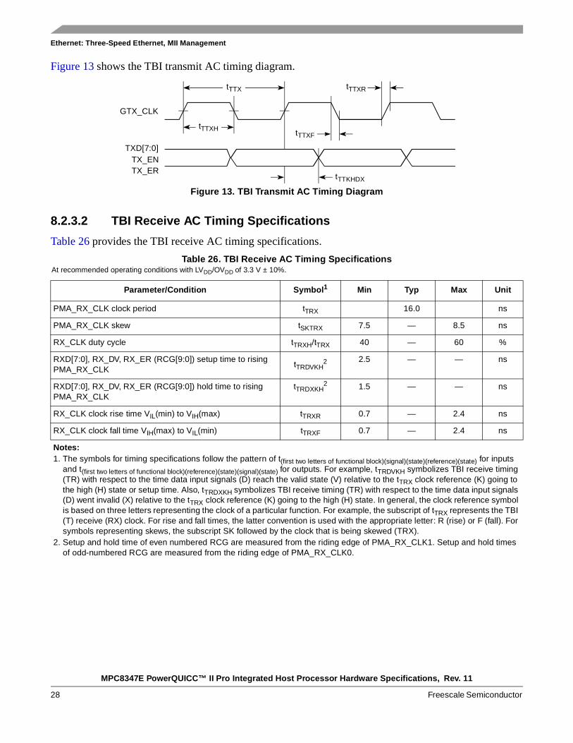
Figure 13 shows the TBI transmit AC timing diagram.
Figure 13. TBI Transmit AC Timing Diagram
8.2.3.2 TBI Receive AC Timing Specifications
Table 26 provides the TBI receive AC timing specifications.
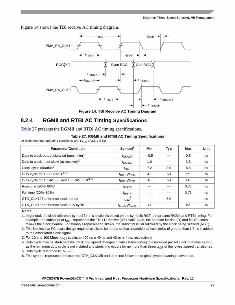
Table 26. TBI Receive AC Timing SpecificationsAt recommended operating conditions with LVDD/OVDD of 3.3 V ± 10%.
Parameter/Condition Symbol1 Min Typ Max Unit
PMA_RX_CLK clock period tTRX 16.0 ns
PMA_RX_CLK skew tSKTRX 7.5 — 8.5 ns
RX_CLK duty cycle tTRXH/tTRX 40 — 60 %
RXD[7:0], RX_DV, RX_ER (RCG[9:0]) setup time to rising PMA_RX_CLK
tTRDVKH2 2.5 — — ns
RXD[7:0], RX_DV, RX_ER (RCG[9:0]) hold time to rising PMA_RX_CLK
tTRDXKH2 1.5 — — ns
RX_CLK clock rise time VIL(min) to VIH(max) tTRXR 0.7 — 2.4 ns
RX_CLK clock fall time VIH(max) to VIL(min) tTRXF 0.7 — 2.4 ns
Notes:1. The symbols for timing specifications follow the pattern of t(first two letters of functional block)(signal)(state)(reference)(state) for inputs
and t(first two letters of functional block)(reference)(state)(signal)(state) for outputs. For example, tTRDVKH symbolizes TBI receive timing (TR) with respect to the time data input signals (D) reach the valid state (V) relative to the tTRX clock reference (K) going to the high (H) state or setup time. Also, tTRDXKH symbolizes TBI receive timing (TR) with respect to the time data input signals (D) went invalid (X) relative to the tTRX clock reference (K) going to the high (H) state. In general, the clock reference symbol is based on three letters representing the clock of a particular function. For example, the subscript of tTRX represents the TBI (T) receive (RX) clock. For rise and fall times, the latter convention is used with the appropriate letter: R (rise) or F (fall). For symbols representing skews, the subscript SK followed by the clock that is being skewed (TRX).
2. Setup and hold time of even numbered RCG are measured from the riding edge of PMA_RX_CLK1. Setup and hold times of odd-numbered RCG are measured from the riding edge of PMA_RX_CLK0.
GTX_CLK
TXD[7:0]
tTTX
tTTXH
tTTXR
tTTXF
tTTKHDX
TX_ENTX_ER
MPC8347E PowerQUICC™ II Pro Integrated Host Processor Hardware Specifications, Rev. 11
Freescale Semiconductor 29
Ethernet: Three-Speed Ethernet, MII Management
Figure 14 shows the TBI receive AC timing diagram.
Figure 14. TBI Receive AC Timing Diagram
8.2.4 RGMII and RTBI AC Timing Specifications
Table 27 presents the RGMII and RTBI AC timing specifications.
Table 27. RGMII and RTBI AC Timing SpecificationsAt recommended operating conditions with LVDD of 2.5 V ± 5%.
Parameter/Condition Symbol1 Min Typ Max Unit
Data to clock output skew (at transmitter) tSKRGT –0.5 — 0.5 ns
Data to clock input skew (at receiver)2 tSKRGT 1.0 — 2.8 ns
Clock cycle duration3 tRGT 7.2 8.0 8.8 ns
Duty cycle for 1000Base-T4, 5 tRGTH/tRGT 45 50 55 %
Duty cycle for 10BASE-T and 100BASE-TX3, 5 tRGTH/tRGT 40 50 60 %
Rise time (20%–80%) tRGTR — — 0.75 ns
Fall time (20%–80%) tRGTF — — 0.75 ns
GTX_CLK125 reference clock period tG126 — 8.0 — ns
GTX_CLK125 reference clock duty cycle tG125H/tG125 47 — 53 %
Notes:1. In general, the clock reference symbol for this section is based on the symbols RGT to represent RGMII and RTBI timing. For
example, the subscript of tRGT represents the TBI (T) receive (RX) clock. Also, the notation for rise (R) and fall (F) times follows the clock symbol. For symbols representing skews, the subscript is SK followed by the clock being skewed (RGT).
2. This implies that PC board design requires clocks to be routed so that an additional trace delay of greater than 1.5 ns is added to the associated clock signal.
3. For 10 and 100 Mbps, tRGT scales to 400 ns ± 40 ns and 40 ns ± 4 ns, respectively.4. Duty cycle may be stretched/shrunk during speed changes or while transitioning to a received packet clock domains as long
as the minimum duty cycle is not violated and stretching occurs for no more than three tRGT of the lowest speed transitioned.5. Duty cycle reference is LVDD/2.6. This symbol represents the external GTX_CLK125 and does not follow the original symbol naming convention.
PMA_RX_CLK1
RCG[9:0]
tTRX
tTRXH
tTRXR
tTRXF
tTRDVKH
PMA_RX_CLK0
tTRDXKH
tTRDVKH
tTRDXKHtTRXH
Even RCG Odd RCG
tSKTRX
MPC8347E PowerQUICC™ II Pro Integrated Host Processor Hardware Specifications, Rev. 11
30 Freescale Semiconductor
Ethernet: Three-Speed Ethernet, MII Management
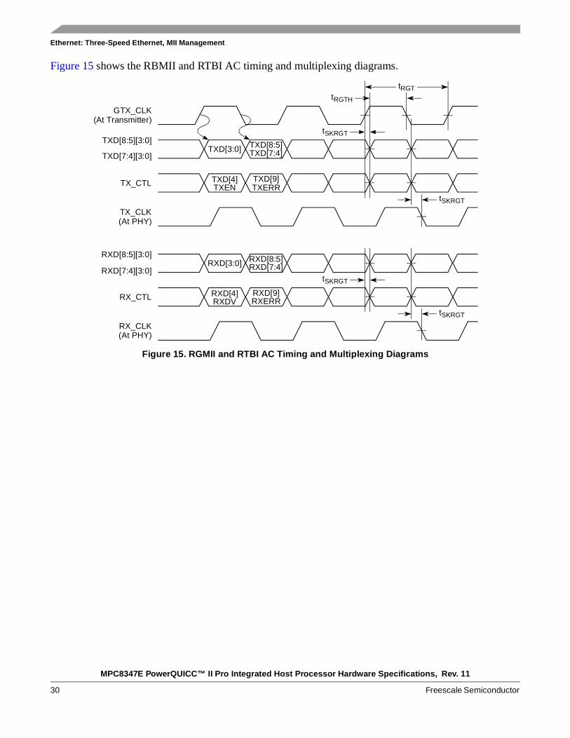
Figure 15 shows the RBMII and RTBI AC timing and multiplexing diagrams.
Figure 15. RGMII and RTBI AC Timing and Multiplexing Diagrams
GTX_CLK
tRGTtRGTH
tSKRGT
TX_CTL
TXD[8:5]TXD[7:4]
TXD[9]TXERR
TXD[4]TXEN
TXD[3:0]
(At Transmitter)
TXD[8:5][3:0]
TXD[7:4][3:0]
TX_CLK(At PHY)
RX_CTL
RXD[8:5]RXD[7:4]
RXD[9]RXERR
RXD[4]RXDV
RXD[3:0]RXD[8:5][3:0]
RXD[7:4][3:0]
RX_CLK(At PHY)
tSKRGT
tSKRGT
tSKRGT
MPC8347E PowerQUICC™ II Pro Integrated Host Processor Hardware Specifications, Rev. 11
Freescale Semiconductor 31
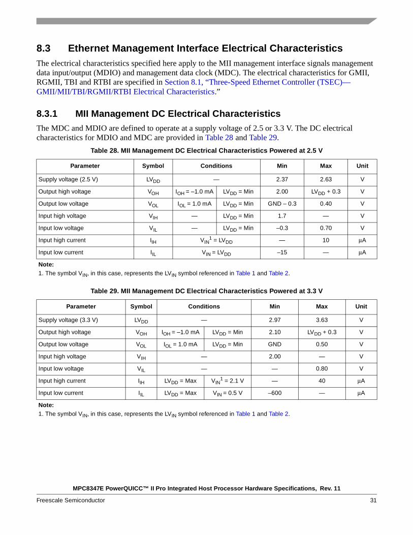
8.3 Ethernet Management Interface Electrical CharacteristicsThe electrical characteristics specified here apply to the MII management interface signals management data input/output (MDIO) and management data clock (MDC). The electrical characteristics for GMII, RGMII, TBI and RTBI are specified in Section 8.1, “Three-Speed Ethernet Controller (TSEC)— GMII/MII/TBI/RGMII/RTBI Electrical Characteristics.”
8.3.1 MII Management DC Electrical CharacteristicsThe MDC and MDIO are defined to operate at a supply voltage of 2.5 or 3.3 V. The DC electrical characteristics for MDIO and MDC are provided in Table 28 and Table 29.
Table 28. MII Management DC Electrical Characteristics Powered at 2.5 V
Parameter Symbol Conditions Min Max Unit
Supply voltage (2.5 V) LVDD — 2.37 2.63 V
Output high voltage VOH IOH = –1.0 mA LVDD = Min 2.00 LVDD + 0.3 V
Output low voltage VOL IOL = 1.0 mA LVDD = Min GND – 0.3 0.40 V
Input high voltage VIH — LVDD = Min 1.7 — V
Input low voltage VIL — LVDD = Min –0.3 0.70 V
Input high current IIH VIN1 = LVDD — 10 μA
Input low current IIL VIN = LVDD –15 — μA
Note:1. The symbol VIN, in this case, represents the LVIN symbol referenced in Table 1 and Table 2.
Table 29. MII Management DC Electrical Characteristics Powered at 3.3 V
Parameter Symbol Conditions Min Max Unit
Supply voltage (3.3 V) LVDD — 2.97 3.63 V
Output high voltage VOH IOH = –1.0 mA LVDD = Min 2.10 LVDD + 0.3 V
Output low voltage VOL IOL = 1.0 mA LVDD = Min GND 0.50 V
Input high voltage VIH — 2.00 — V
Input low voltage VIL — — 0.80 V
Input high current IIH LVDD = Max VIN1 = 2.1 V — 40 μA
Input low current IIL LVDD = Max VIN = 0.5 V –600 — μA
Note:1. The symbol VIN, in this case, represents the LVIN symbol referenced in Table 1 and Table 2.
MPC8347E PowerQUICC™ II Pro Integrated Host Processor Hardware Specifications, Rev. 11
32 Freescale Semiconductor
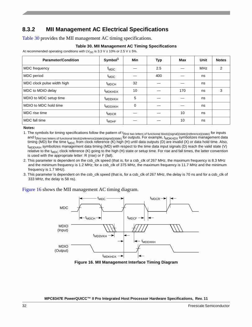
8.3.2 MII Management AC Electrical SpecificationsTable 30 provides the MII management AC timing specifications.
Figure 16 shows the MII management AC timing diagram.
Figure 16. MII Management Interface Timing Diagram
Table 30. MII Management AC Timing SpecificationsAt recommended operating conditions with LVDD is 3.3 V ± 10% or 2.5 V ± 5%.
Parameter/Condition Symbol1 Min Typ Max Unit Notes
MDC frequency fMDC — 2.5 — MHz 2
MDC period tMDC — 400 — ns
MDC clock pulse width high tMDCH 32 — — ns
MDC to MDIO delay tMDKHDX 10 — 170 ns 3
MDIO to MDC setup time tMDDVKH 5 — — ns
MDIO to MDC hold time tMDDXKH 0 — — ns
MDC rise time tMDCR — — 10 ns
MDC fall time tMDHF — — 10 ns
Notes:1. The symbols for timing specifications follow the pattern of t(first two letters of functional block)(signal)(state)(reference)(state) for inputs
and t(first two letters of functional block)(reference)(state)(signal)(state) for outputs. For example, tMDKHDX symbolizes management data timing (MD) for the time tMDC from clock reference (K) high (H) until data outputs (D) are invalid (X) or data hold time. Also, tMDDVKH symbolizes management data timing (MD) with respect to the time data input signals (D) reach the valid state (V) relative to the tMDC clock reference (K) going to the high (H) state or setup time. For rise and fall times, the latter convention is used with the appropriate letter: R (rise) or F (fall).
2. This parameter is dependent on the csb_clk speed (that is, for a csb_clk of 267 MHz, the maximum frequency is 8.3 MHz and the minimum frequency is 1.2 MHz; for a csb_clk of 375 MHz, the maximum frequency is 11.7 MHz and the minimum frequency is 1.7 MHz).
3. This parameter is dependent on the csb_clk speed (that is, for a csb_clk of 267 MHz, the delay is 70 ns and for a csb_clk of 333 MHz, the delay is 58 ns).
MDC
tMDDXKH
tMDC
tMDCH
tMDCR
tMDCF
tMDDVKH
tMDKHDX
MDIO
MDIO
(Input)
(Output)
MPC8347E PowerQUICC™ II Pro Integrated Host Processor Hardware Specifications, Rev. 11
Freescale Semiconductor 33
USB
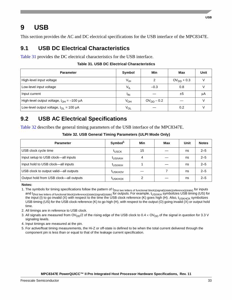
9 USBThis section provides the AC and DC electrical specifications for the USB interface of the MPC8347E.
9.1 USB DC Electrical CharacteristicsTable 31 provides the DC electrical characteristics for the USB interface.
9.2 USB AC Electrical SpecificationsTable 32 describes the general timing parameters of the USB interface of the MPC8347E.
Table 31. USB DC Electrical Characteristics
Parameter Symbol Min Max Unit
High-level input voltage VIH 2 OVDD + 0.3 V
Low-level input voltage VIL –0.3 0.8 V
Input current IIN — ±5 μA
High-level output voltage, IOH = –100 μA VOH OVDD – 0.2 — V
Low-level output voltage, IOL = 100 μA VOL — 0.2 V
Table 32. USB General Timing Parameters (ULPI Mode Only)
Parameter Symbol1 Min Max Unit Notes
USB clock cycle time tUSCK 15 — ns 2–5
Input setup to USB clock—all inputs tUSIVKH 4 — ns 2–5
Input hold to USB clock—all inputs tUSIXKH 1 — ns 2–5
USB clock to output valid—all outputs tUSKHOV — 7 ns 2–5
Output hold from USB clock—all outputs tUSKHOX 2 — ns 2–5
Notes:1. The symbols for timing specifications follow the pattern of t(first two letters of functional block)(signal)(state)(reference)(state) for inputs
and t(first two letters of functional block)(reference)(state)(signal)(state) for outputs. For example, tUSIXKH symbolizes USB timing (US) for the input (I) to go invalid (X) with respect to the time the USB clock reference (K) goes high (H). Also, tUSKHOX symbolizes USB timing (US) for the USB clock reference (K) to go high (H), with respect to the output (O) going invalid (X) or output hold time.
2. All timings are in reference to USB clock.3. All signals are measured from OVDD/2 of the rising edge of the USB clock to 0.4 × OVDD of the signal in question for 3.3 V
signaling levels.4. Input timings are measured at the pin.5. For active/float timing measurements, the Hi-Z or off-state is defined to be when the total current delivered through the
component pin is less than or equal to that of the leakage current specification.
MPC8347E PowerQUICC™ II Pro Integrated Host Processor Hardware Specifications, Rev. 11
34 Freescale Semiconductor
USB
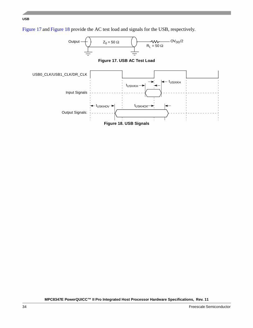
Figure 17 and Figure 18 provide the AC test load and signals for the USB, respectively.
Figure 17. USB AC Test Load
Figure 18. USB Signals
Output Z0 = 50 Ω OVDD/2RL = 50 Ω
Output Signals:
tUSKHOV
USB0_CLK/USB1_CLK/DR_CLK
Input Signals
tUSIXKHtUSIVKH
tUSKHOX
MPC8347E PowerQUICC™ II Pro Integrated Host Processor Hardware Specifications, Rev. 11
Freescale Semiconductor 35
Local Bus
10 Local BusThis section describes the DC and AC electrical specifications for the local bus interface of the MPC8347E.
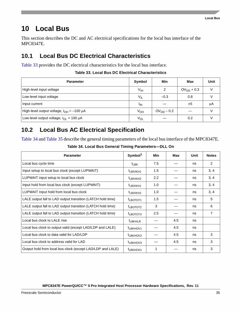
10.1 Local Bus DC Electrical CharacteristicsTable 33 provides the DC electrical characteristics for the local bus interface.
10.2 Local Bus AC Electrical SpecificationTable 34 and Table 35 describe the general timing parameters of the local bus interface of the MPC8347E.
Table 33. Local Bus DC Electrical Characteristics
Parameter Symbol Min Max Unit
High-level input voltage VIH 2 OVDD + 0.3 V
Low-level input voltage VIL –0.3 0.8 V
Input current IIN — ±5 μA
High-level output voltage, IOH = –100 μA VOH OVDD – 0.2 — V
Low-level output voltage, IOL = 100 μA VOL — 0.2 V
Table 34. Local Bus General Timing Parameters—DLL On
Parameter Symbol1 Min Max Unit Notes
Local bus cycle time tLBK 7.5 — ns 2
Input setup to local bus clock (except LUPWAIT) tLBIVKH1 1.5 — ns 3, 4
LUPWAIT input setup to local bus clock tLBIVKH2 2.2 — ns 3, 4
Input hold from local bus clock (except LUPWAIT) tLBIXKH1 1.0 — ns 3, 4
LUPWAIT Input hold from local bus clock tLBIXKH2 1.0 — ns 3, 4
LALE output fall to LAD output transition (LATCH hold time) tLBOTOT1 1.5 — ns 5
LALE output fall to LAD output transition (LATCH hold time) tLBOTOT2 3 — ns 6
LALE output fall to LAD output transition (LATCH hold time) tLBOTOT3 2.5 — ns 7
Local bus clock to LALE rise tLBKHLR — 4.5 ns
Local bus clock to output valid (except LAD/LDP and LALE) tLBKHOV1 — 4.5 ns
Local bus clock to data valid for LAD/LDP tLBKHOV2 — 4.5 ns 3
Local bus clock to address valid for LAD tLBKHOV3 — 4.5 ns 3
Output hold from local bus clock (except LAD/LDP and LALE) tLBKHOX1 1 — ns 3
MPC8347E PowerQUICC™ II Pro Integrated Host Processor Hardware Specifications, Rev. 11
36 Freescale Semiconductor
Local Bus
Output hold from local bus clock for LAD/LDP tLBKHOX2 1 — ns 3
Local bus clock to output high impedance for LAD/LDP tLBKHOZ — 3.8 ns 8
Notes:1. The symbols for timing specifications follow the pattern of t(first two letters of functional block)(signal)(state)(reference)(state) for inputs
and t(first two letters of functional block)(reference)(state)(signal)(state) for outputs. For example, tLBIXKH1 symbolizes local bus timing (LB) for the input (I) to go invalid (X) with respect to the time the tLBK clock reference (K) goes high (H), in this case for clock one (1). Also, tLBKHOX symbolizes local bus timing (LB) for the tLBK clock reference (K) to go high (H), with respect to the output (O) going invalid (X) or output hold time.
2. All timings are in reference to the rising edge of LSYNC_IN.3. All signals are measured from OVDD/2 of the rising edge of LSYNC_IN to 0.4 × OVDD of the signal in question for 3.3 V
signaling levels.4. Input timings are measured at the pin.5. tLBOTOT1 should be used when RCWH[LALE] is not set and when the load on the LALE output pin is at least 10 pF less than
the load on the LAD output pins.6. tLBOTOT2 should be used when RCWH[LALE] is set and when the load on the LALE output pin is at least 10 pF less than the
load on the LAD output pins.7. tLBOTOT3 should be used when RCWH[LALE] is set and when the load on the LALE output pin equals the load on the LAD
output pins. 8. For active/float timing measurements, the Hi-Z or off-state is defined to be when the total current delivered through the
component pin is less than or equal to that of the leakage current specification.
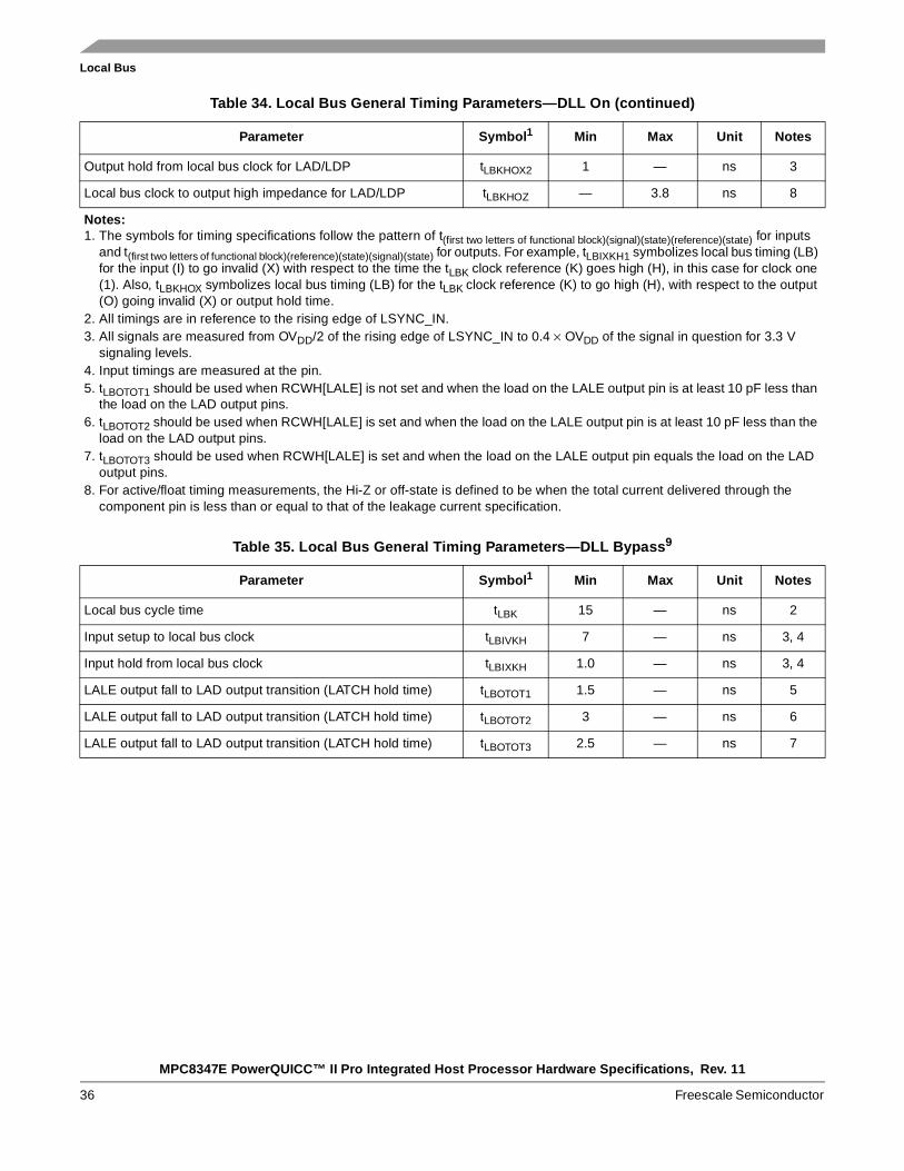
Table 35. Local Bus General Timing Parameters—DLL Bypass9
Parameter Symbol1 Min Max Unit Notes
Local bus cycle time tLBK 15 — ns 2
Input setup to local bus clock tLBIVKH 7 — ns 3, 4
Input hold from local bus clock tLBIXKH 1.0 — ns 3, 4
LALE output fall to LAD output transition (LATCH hold time) tLBOTOT1 1.5 — ns 5
LALE output fall to LAD output transition (LATCH hold time) tLBOTOT2 3 — ns 6
LALE output fall to LAD output transition (LATCH hold time) tLBOTOT3 2.5 — ns 7
Table 34. Local Bus General Timing Parameters—DLL On (continued)
Parameter Symbol1 Min Max Unit Notes
MPC8347E PowerQUICC™ II Pro Integrated Host Processor Hardware Specifications, Rev. 11
Freescale Semiconductor 37
Local Bus
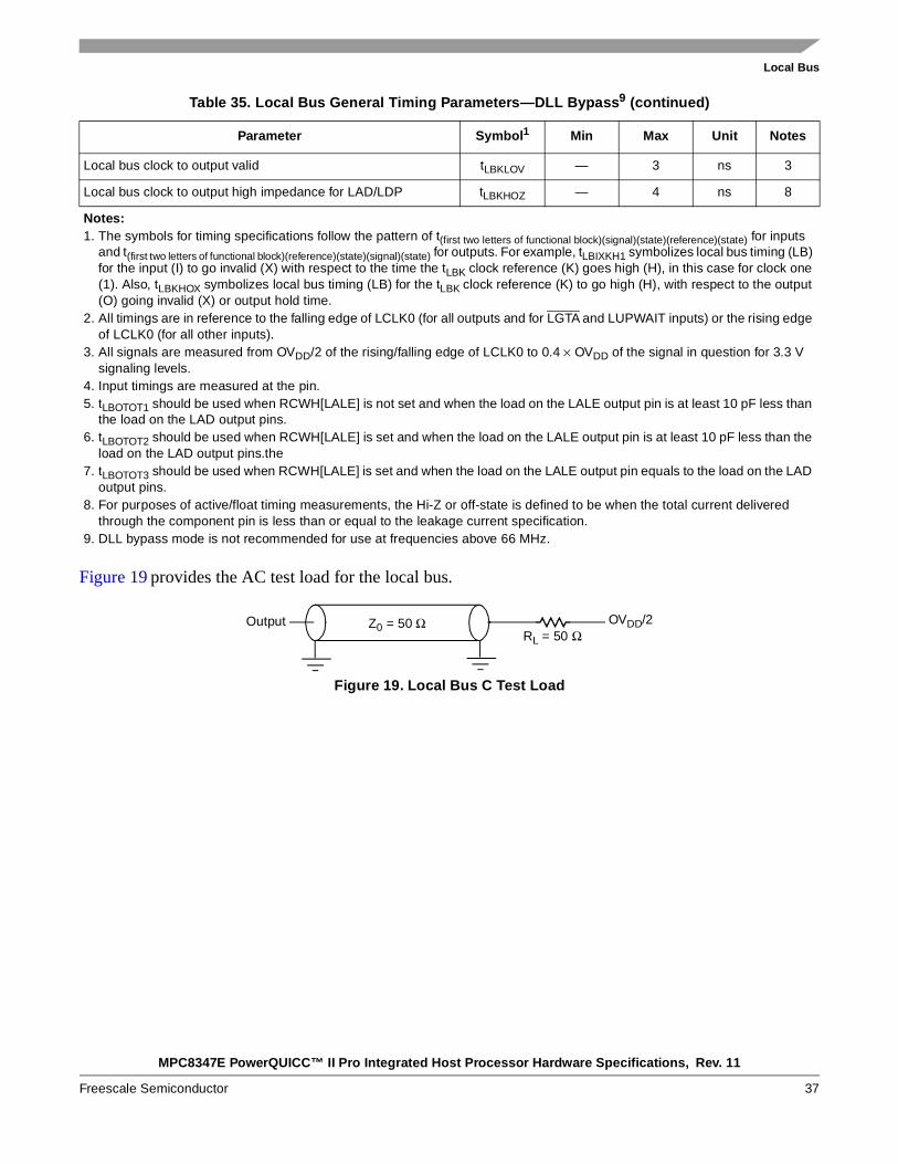
Figure 19 provides the AC test load for the local bus.
Figure 19. Local Bus C Test Load
Local bus clock to output valid tLBKLOV — 3 ns 3
Local bus clock to output high impedance for LAD/LDP tLBKHOZ — 4 ns 8
Notes:1. The symbols for timing specifications follow the pattern of t(first two letters of functional block)(signal)(state)(reference)(state) for inputs
and t(first two letters of functional block)(reference)(state)(signal)(state) for outputs. For example, tLBIXKH1 symbolizes local bus timing (LB) for the input (I) to go invalid (X) with respect to the time the tLBK clock reference (K) goes high (H), in this case for clock one (1). Also, tLBKHOX symbolizes local bus timing (LB) for the tLBK clock reference (K) to go high (H), with respect to the output (O) going invalid (X) or output hold time.
2. All timings are in reference to the falling edge of LCLK0 (for all outputs and for LGTA and LUPWAIT inputs) or the rising edge of LCLK0 (for all other inputs).
3. All signals are measured from OVDD/2 of the rising/falling edge of LCLK0 to 0.4 × OVDD of the signal in question for 3.3 V signaling levels.
4. Input timings are measured at the pin.5. tLBOTOT1 should be used when RCWH[LALE] is not set and when the load on the LALE output pin is at least 10 pF less than
the load on the LAD output pins.6. tLBOTOT2 should be used when RCWH[LALE] is set and when the load on the LALE output pin is at least 10 pF less than the
load on the LAD output pins.the 7. tLBOTOT3 should be used when RCWH[LALE] is set and when the load on the LALE output pin equals to the load on the LAD
output pins. 8. For purposes of active/float timing measurements, the Hi-Z or off-state is defined to be when the total current delivered
through the component pin is less than or equal to the leakage current specification.9. DLL bypass mode is not recommended for use at frequencies above 66 MHz.
Table 35. Local Bus General Timing Parameters—DLL Bypass9 (continued)
Parameter Symbol1 Min Max Unit Notes
Output Z0 = 50 Ω OVDD/2RL = 50 Ω
MPC8347E PowerQUICC™ II Pro Integrated Host Processor Hardware Specifications, Rev. 11
38 Freescale Semiconductor
Local Bus
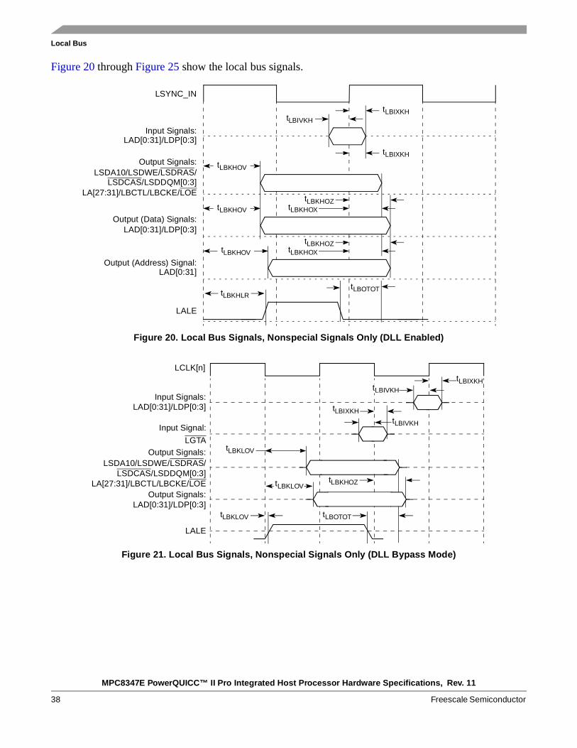
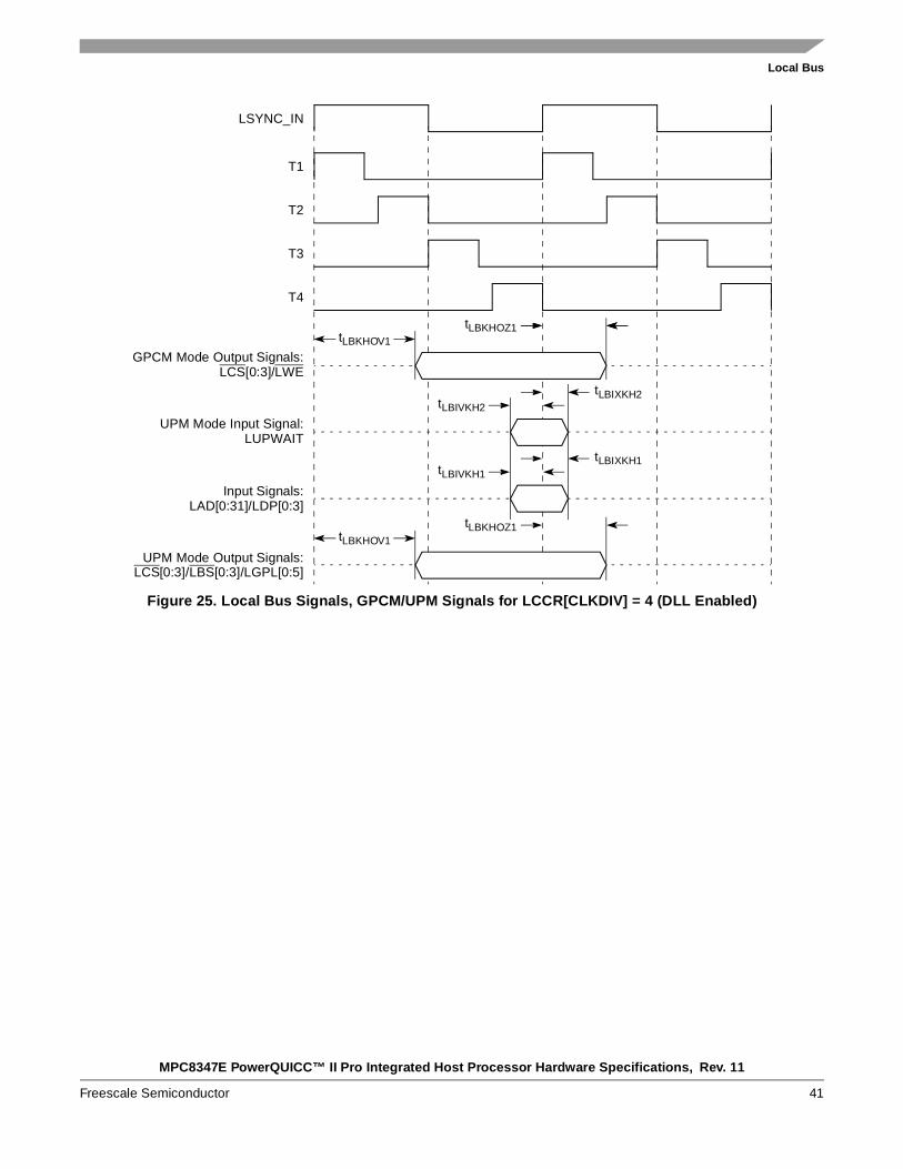
Figure 20 through Figure 25 show the local bus signals.
Figure 20. Local Bus Signals, Nonspecial Signals Only (DLL Enabled)
Figure 21. Local Bus Signals, Nonspecial Signals Only (DLL Bypass Mode)
Output Signals:
LA[27:31]/LBCTL/LBCKE/LOE
LSDA10/LSDWE/LSDRAS/LSDCAS/LSDDQM[0:3]
tLBKHOV
tLBKHOV
tLBKHOV
LSYNC_IN
Input Signals:LAD[0:31]/LDP[0:3]
Output (Data) Signals:LAD[0:31]/LDP[0:3]
Output (Address) Signal:LAD[0:31]
LALE
tLBIXKHtLBIVKH
tLBIXKH
tLBKHOX
tLBKHOZ
tLBKHLRtLBOTOT
tLBKHOZtLBKHOX
Output Signals:LSDA10/LSDWE/LSDRAS/
LSDCAS/LSDDQM[0:3]
LCLK[n]
Input Signals:LAD[0:31]/LDP[0:3]
Output Signals:LAD[0:31]/LDP[0:3]
LALE
Input Signal:
LGTA
tLBIXKH
tLBKLOV
tLBKHOZ
tLBOTOT
tLBIVKH
tLBIXKH
tLBKLOV
tLBKLOV
tLBIVKH
LA[27:31]/LBCTL/LBCKE/LOE
MPC8347E PowerQUICC™ II Pro Integrated Host Processor Hardware Specifications, Rev. 11
Freescale Semiconductor 39
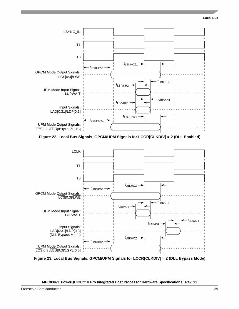
Local Bus
Figure 22. Local Bus Signals, GPCM/UPM Signals for LCCR[CLKDIV] = 2 (DLL Enabled)
Figure 23. Local Bus Signals, GPCM/UPM Signals for LCCR[CLKDIV] = 2 (DLL Bypass Mode)
LSYNC_IN
UPM Mode Input Signal:LUPWAIT
tLBIXKH2tLBIVKH2
tLBIVKH1
tLBIXKH1
tLBKHOZ1
T1
T3
Input Signals:LAD[0:31]/LDP[0:3]
UPM Mode Output Signals:LCS[0:3]/LBS[0:3]/LGPL[0:5]
GPCM Mode Output Signals:LCS[0:3]/LWE
tLBKHOV1
tLBKHOV1
tLBKHOZ1
UPM Mode Output Signals:
LCLK
UPM Mode Input Signal:LUPWAIT
tLBIXKHtLBIVKH
tLBIVKH
tLBIXKH
tLBKHOZ
T1
T3
Input Signals:LAD[0:31]/LDP[0:3]
UPM Mode Output Signals:LCS[0:3]/LBS[0:3]/LGPL[0:5]
GPCM Mode Output Signals:LCS[0:3]/LWE
tLBKHOV
tLBKHOV
tLBKHOZ
(DLL Bypass Mode)
MPC8347E PowerQUICC™ II Pro Integrated Host Processor Hardware Specifications, Rev. 11
40 Freescale Semiconductor
Local Bus
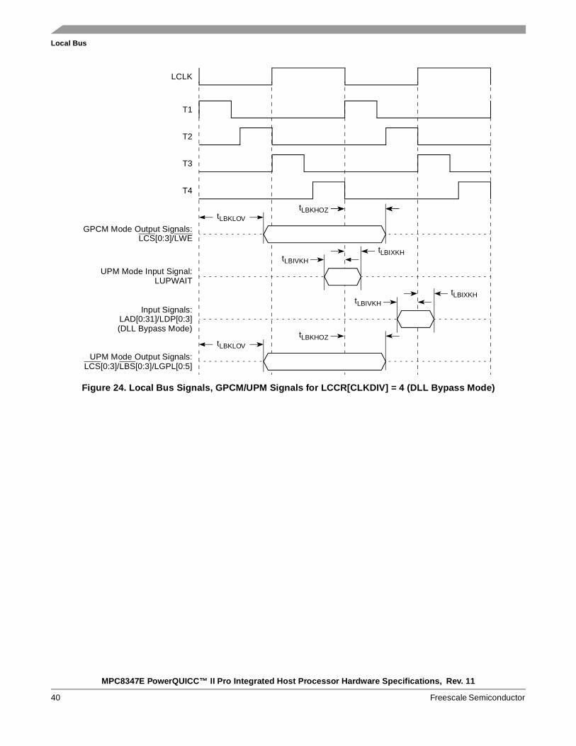
Figure 24. Local Bus Signals, GPCM/UPM Signals for LCCR[CLKDIV] = 4 (DLL Bypass Mode)
LCLK
UPM Mode Input Signal:LUPWAIT
tLBIXKHtLBIVKH
tLBIVKH
tLBIXKH
tLBKHOZ
T1
T3
UPM Mode Output Signals:LCS[0:3]/LBS[0:3]/LGPL[0:5]
GPCM Mode Output Signals:LCS[0:3]/LWE
tLBKLOV
tLBKLOV
tLBKHOZ
T2
T4
Input Signals:LAD[0:31]/LDP[0:3](DLL Bypass Mode)
MPC8347E PowerQUICC™ II Pro Integrated Host Processor Hardware Specifications, Rev. 11
Freescale Semiconductor 41
Local Bus
Figure 25. Local Bus Signals, GPCM/UPM Signals for LCCR[CLKDIV] = 4 (DLL Enabled)
LSYNC_IN
UPM Mode Input Signal:LUPWAIT
tLBIXKH2tLBIVKH2
tLBIVKH1
tLBIXKH1
tLBKHOZ1
T1
T3
Input Signals:LAD[0:31]/LDP[0:3]
UPM Mode Output Signals:LCS[0:3]/LBS[0:3]/LGPL[0:5]
GPCM Mode Output Signals:LCS[0:3]/LWE
tLBKHOV1
tLBKHOV1
tLBKHOZ1
T2
T4
MPC8347E PowerQUICC™ II Pro Integrated Host Processor Hardware Specifications, Rev. 11
42 Freescale Semiconductor
JTAG
11 JTAGThis section describes the DC and AC electrical specifications for the IEEE Std. 1149.1 (JTAG) interface of the MPC8347E
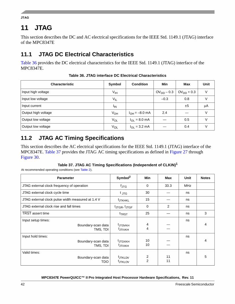
11.1 JTAG DC Electrical CharacteristicsTable 36 provides the DC electrical characteristics for the IEEE Std. 1149.1 (JTAG) interface of the MPC8347E.
11.2 JTAG AC Timing SpecificationsThis section describes the AC electrical specifications for the IEEE Std. 1149.1 (JTAG) interface of the MPC8347E. Table 37 provides the JTAG AC timing specifications as defined in Figure 27 through Figure 30.
Table 36. JTAG interface DC Electrical Characteristics
Characteristic Symbol Condition Min Max Unit
Input high voltage VIH OVDD – 0.3 OVDD + 0.3 V
Input low voltage VIL –0.3 0.8 V
Input current IIN ±5 μA
Output high voltage VOH IOH = –8.0 mA 2.4 — V
Output low voltage VOL IOL = 8.0 mA — 0.5 V
Output low voltage VOL IOL = 3.2 mA — 0.4 V
Table 37. JTAG AC Timing Specifications (Independent of CLKIN)1
At recommended operating conditions (see Table 2).
Parameter Symbol2 Min Max Unit Notes
JTAG external clock frequency of operation fJTG 0 33.3 MHz
JTAG external clock cycle time t JTG 30 — ns
JTAG external clock pulse width measured at 1.4 V tJTKHKL 15 — ns
JTAG external clock rise and fall times tJTGR, tJTGF 0 2 ns
TRST assert time tTRST 25 — ns 3
Input setup times:
Boundary-scan dataTMS, TDI
tJTDVKHtJTIVKH
44
——
ns4
Input hold times:
Boundary-scan dataTMS, TDI
tJTDXKHtJTIXKH
1010
——
ns4
Valid times:
Boundary-scan dataTDO
tJTKLDVtJTKLOV
22
1111
ns5
MPC8347E PowerQUICC™ II Pro Integrated Host Processor Hardware Specifications, Rev. 11
Freescale Semiconductor 43
JTAG
Figure 26 provides the AC test load for TDO and the boundary-scan outputs of the MPC8347E.
Figure 26. AC Test Load for the JTAG Interface
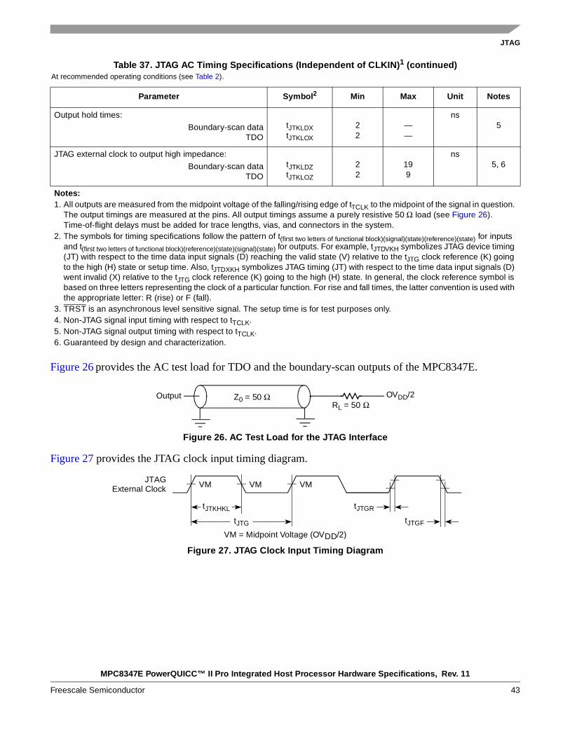
Figure 27 provides the JTAG clock input timing diagram.
Figure 27. JTAG Clock Input Timing Diagram
Output hold times:
Boundary-scan dataTDO
tJTKLDXtJTKLOX
22
——
ns5
JTAG external clock to output high impedance:
Boundary-scan dataTDO
tJTKLDZtJTKLOZ
22
199
ns5, 6
Notes:1. All outputs are measured from the midpoint voltage of the falling/rising edge of tTCLK to the midpoint of the signal in question.
The output timings are measured at the pins. All output timings assume a purely resistive 50 Ω load (see Figure 26). Time-of-flight delays must be added for trace lengths, vias, and connectors in the system.
2. The symbols for timing specifications follow the pattern of t(first two letters of functional block)(signal)(state)(reference)(state) for inputs and t(first two letters of functional block)(reference)(state)(signal)(state) for outputs. For example, tJTDVKH symbolizes JTAG device timing (JT) with respect to the time data input signals (D) reaching the valid state (V) relative to the tJTG clock reference (K) going to the high (H) state or setup time. Also, tJTDXKH symbolizes JTAG timing (JT) with respect to the time data input signals (D) went invalid (X) relative to the tJTG clock reference (K) going to the high (H) state. In general, the clock reference symbol is based on three letters representing the clock of a particular function. For rise and fall times, the latter convention is used with the appropriate letter: R (rise) or F (fall).
3. TRST is an asynchronous level sensitive signal. The setup time is for test purposes only.4. Non-JTAG signal input timing with respect to tTCLK.5. Non-JTAG signal output timing with respect to tTCLK.6. Guaranteed by design and characterization.
Table 37. JTAG AC Timing Specifications (Independent of CLKIN)1 (continued)At recommended operating conditions (see Table 2).
Parameter Symbol2 Min Max Unit Notes
Output Z0 = 50 Ω OVDD/2RL = 50 Ω
JTAG
tJTKHKL tJTGR
External Clock VMVMVM
tJTG tJTGF
VM = Midpoint Voltage (OVDD/2)
MPC8347E PowerQUICC™ II Pro Integrated Host Processor Hardware Specifications, Rev. 11
44 Freescale Semiconductor
JTAG
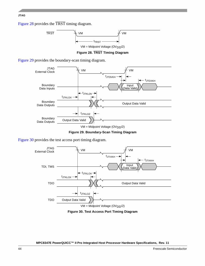
Figure 28 provides the TRST timing diagram.
Figure 28. TRST Timing Diagram
Figure 29 provides the boundary-scan timing diagram.
Figure 29. Boundary-Scan Timing Diagram
Figure 30 provides the test access port timing diagram.
Figure 30. Test Access Port Timing Diagram
TRST
VM = Midpoint Voltage (OVDD/2)
VM VM
tTRST
VM = Midpoint Voltage (OVDD/2)
VM VM
tJTDVKHtJTDXKH
BoundaryData Outputs
BoundaryData Outputs
JTAGExternal Clock
BoundaryData Inputs
Output Data Valid
tJTKLDX
tJTKLDZ
tJTKLDV
InputData Valid
Output Data Valid
VM = Midpoint Voltage (OVDD/2)
VM VM
tJTIVKHtJTIXKH
JTAGExternal Clock
Output Data Valid
tJTKLOX
tJTKLOZ
tJTKLOV
InputData Valid
Output Data Valid
TDI, TMS
TDO
TDO
MPC8347E PowerQUICC™ II Pro Integrated Host Processor Hardware Specifications, Rev. 11
Freescale Semiconductor 45
I2C
12 I2C This section describes the DC and AC electrical characteristics for the I2C interface of the MPC8347E.
12.1 I2C DC Electrical CharacteristicsTable 38 provides the DC electrical characteristics for the I2C interface of the MPC8347E.
12.2 I2C AC Electrical SpecificationsTable 39 provides the AC timing parameters for the I2C interface of the MPC8347E. Note that all values refer to VIH(min) and VIL(max) levels (see Table 38).
Table 38. I2C DC Electrical CharacteristicsAt recommended operating conditions with OVDD of 3.3 V ± 10%.
Parameter Symbol Min Max Unit Notes
Input high voltage level VIH 0.7 × OVDD OVDD + 0.3 V
Input low voltage level VIL –0.3 0.3 × OVDD V
Low level output voltage VOL 0 0.2 × OVDD V 1
Output fall time from VIH(min) to VIL(max) with a bus capacitance from 10 to 400 pF
tI2KLKV 20 + 0.1 × CB 250 ns 2
Pulse width of spikes which must be suppressed by the input filter
tI2KHKL 0 50 ns 3
Input current each I/O pin (input voltage is between 0.1 × OVDD and 0.9 × OVDD(max)
II –10 10 μA 4
Capacitance for each I/O pin CI — 10 pF
Notes:1. Output voltage (open drain or open collector) condition = 3 mA sink current.2. CB = capacitance of one bus line in pF.3. Refer to the MPC8349E Integrated Host Processor Family Reference Manual, for information on the digital filter used.4. I/O pins obstruct the SDA and SCL lines if OVDD is switched off.
Table 39. I2C AC Electrical Specifications
Parameter Symbol1 Min Max Unit
SCL clock frequency fI2C 0 400 kHz
Low period of the SCL clock tI2CL 1.3 — μs
High period of the SCL clock tI2CH 0.6 — μs
Setup time for a repeated START condition tI2SVKH 0.6 — μs
Hold time (repeated) START condition (after this period, the first clock pulse is generated)
tI2SXKL 0.6 — μs
Data setup time tI2DVKH 100 — ns
Data hold time: CBUS compatible mastersI2C bus devices
tI2DXKL —02
—0.93
μs
MPC8347E PowerQUICC™ II Pro Integrated Host Processor Hardware Specifications, Rev. 11
46 Freescale Semiconductor
I2C
Figure 31 provides the AC test load for the I2C.
Figure 31. I2C AC Test Load
Figure 32 shows the AC timing diagram for the I2C bus.
Figure 32. I2C Bus AC Timing Diagram
Fall time of both SDA and SCL signals5 tI2CF__ 300 ns
Setup time for STOP condition tI2PVKH 0.6 — μs
Bus free time between a STOP and START condition tI2KHDX 1.3 — μs
Noise margin at the LOW level for each connected device (including hysteresis)
VNL 0.1 × OVDD — V
Noise margin at the HIGH level for each connected device (including hysteresis)
VNH 0.2 × OVDD — V
Notes:1. The symbols for timing specifications follow the pattern of t(first two letters of functional block)(signal)(state)(reference)(state) for inputs
and t(first two letters of functional block)(reference)(state)(signal)(state) for outputs. For example, tI2DVKH symbolizes I2C timing (I2) with respect to the time data input signals (D) reach the valid state (V) relative to the tI2C clock reference (K) going to the high (H) state or setup time. Also, tI2SXKL symbolizes I2C timing (I2) for the time that the data with respect to the start condition (S) goes invalid (X) relative to the tI2C clock reference (K) going to the low (L) state or hold time. Also, tI2PVKH symbolizes I2C timing (I2) for the time that the data with respect to the stop condition (P) reaches the valid state (V) relative to the tI2C clock reference (K) going to the high (H) state or setup time. For rise and fall times, the latter convention is used with the appropriate letter: R (rise) or F (fall).
2. MPC8347E provides a hold time of at least 300 ns for the SDA signal (referred to the VIH(min) of the SCL signal) to bridge the undefined region of the falling edge of SCL.
3. The maximum tI2DVKH must be met only if the device does not stretch the LOW period (tI2CL) of the SCL signal.4. CB = capacitance of one bus line in pF.5.)The MPC8347E does not follow the “I2C-BUS Specifications” version 2.1 regarding the tI2CF AC parameter.
Table 39. I2C AC Electrical Specifications (continued)
Parameter Symbol1 Min Max Unit
Output Z0 = 50 Ω OVDD/2RL = 50 Ω
SrS
SDA
SCL
tI2CF
tI2SXKL
tI2CL
tI2CHtI2DXKL
tI2DVKH
tI2SXKL
tI2SVKH
tI2KHKL
tI2PVKH
tI2CR
tI2CF
P S
MPC8347E PowerQUICC™ II Pro Integrated Host Processor Hardware Specifications, Rev. 11
Freescale Semiconductor 47
PCI
13 PCIThis section describes the DC and AC electrical specifications for the PCI bus of the MPC8347E.
13.1 PCI DC Electrical CharacteristicsTable 40 provides the DC electrical characteristics for the PCI interface of the MPC8347E.
13.2 PCI AC Electrical SpecificationsThis section describes the general AC timing parameters of the PCI bus of the MPC8347E. Note that the PCI_CLK or PCI_SYNC_IN signal is used as the PCI input clock depending on whether the MPC8347E is configured as a host or agent device. Table 41 provides the PCI AC timing specifications at 66 MHz.
Table 40. PCI DC Electrical Characteristics
Parameter Symbol Test Condition Min Max Unit
High-level input voltage VIH VOUT ≥ VOH (min) or 2 OVDD + 0.3 V
Low-level input voltage VIL VOUT ≤ VOL (max) –0.3 0.8 V
Input current IIN VIN1= 0 V or VIN = OVDD — ±5 μA
High-level output voltage VOH OVDD = min,IOH = –100 μA
OVDD – 0.2 — V
Low-level output voltage VOL OVDD = min, IOL = 100 μA
— 0.2 V
Note:1. The symbol VIN, in this case, represents the OVIN symbol referenced in Table 1.
Table 41. PCI AC Timing Specifications at 66 MHz1
Parameter Symbol2 Min Max Unit Notes
Clock to output valid tPCKHOV — 6.0 ns 3
Output hold from clock tPCKHOX 1 — ns 3
Clock to output high impedance tPCKHOZ — 14 ns 3, 4
Input setup to clock tPCIVKH 3.0 — ns 3, 5
MPC8347E PowerQUICC™ II Pro Integrated Host Processor Hardware Specifications, Rev. 11
48 Freescale Semiconductor
PCI
Table 42 provides the PCI AC timing specifications at 33 MHz.
Figure 33 provides the AC test load for PCI.
Figure 33. PCI AC Test Load
Input hold from clock tPCIXKH 0 — ns 3, 5
Notes:1. PCI timing depends on M66EN and the ratio between PCI1/PCI2. Refer to the PCI chapter of the reference manual for a
description of M66EN. 2. The symbols for timing specifications follow the pattern of t(first two letters of functional block)(signal)(state)(reference)(state) for inputs
and t(first two letters of functional block)(reference)(state)(signal)(state) for outputs. For example, tPCIVKH symbolizes PCI timing (PC) with respect to the time the input signals (I) reach the valid state (V) relative to the PCI_SYNC_IN clock, tSYS, reference (K) going to the high (H) state or setup time. Also, tPCRHFV symbolizes PCI timing (PC) with respect to the time hard reset (R) went high (H) relative to the frame signal (F) going to the valid (V) state.
3. See the timing measurement conditions in the PCI 2.2 Local Bus Specifications.4. For active/float timing measurements, the Hi-Z or off-state is defined to be when the total current delivered through the
component pin is less than or equal to the leakage current specification.5. Input timings are measured at the pin.
Table 42. PCI AC Timing Specifications at 33 MHz
Parameter Symbol1 Min Max Unit Notes
Clock to output valid tPCKHOV — 11 ns 2
Output hold from clock tPCKHOX 2 — ns 2
Clock to output high impedance tPCKHOZ — 14 ns 2, 3
Input setup to clock tPCIVKH 3.0 — ns 2, 4
Input hold from clock tPCIXKH 0 — ns 2, 4
Notes:1. The symbols for timing specifications follow the pattern of t(first two letters of functional block)(signal)(state)(reference)(state) for inputs
and t(first two letters of functional block)(reference)(state)(signal)(state) for outputs. For example, tPCIVKH symbolizes PCI timing (PC) with respect to the time the input signals (I) reach the valid state (V) relative to the PCI_SYNC_IN clock, tSYS, reference (K) going to the high (H) state or setup time. Also, tPCRHFV symbolizes PCI timing (PC) with respect to the time hard reset (R) went high (H) relative to the frame signal (F) going to the valid (V) state.
2. See the timing measurement conditions in the PCI 2.2 Local Bus Specifications.3. For active/float timing measurements, the Hi-Z or off-state is defined to be when the total current delivered through the
component pin is less than or equal to the leakage current specification.4. Input timings are measured at the pin.
Table 41. PCI AC Timing Specifications at 66 MHz1 (continued)
Parameter Symbol2 Min Max Unit Notes
Output Z0 = 50 Ω OVDD/2RL = 50 Ω
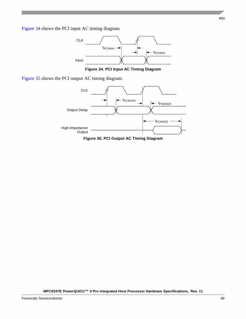
MPC8347E PowerQUICC™ II Pro Integrated Host Processor Hardware Specifications, Rev. 11
Freescale Semiconductor 49
PCI
Figure 34 shows the PCI input AC timing diagram.
Figure 34. PCI Input AC Timing Diagram
Figure 35 shows the PCI output AC timing diagram.
Figure 35. PCI Output AC Timing Diagram
tPCIVKH
CLK
Input
tPCIXKH
CLK
Output Delay
tPCKHOV
High-Impedance
tPCKHOZ
Output
tPCKHOX
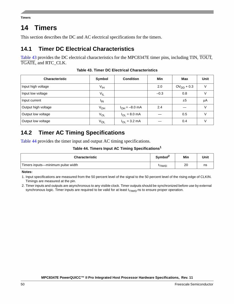
MPC8347E PowerQUICC™ II Pro Integrated Host Processor Hardware Specifications, Rev. 11
50 Freescale Semiconductor
Timers
14 TimersThis section describes the DC and AC electrical specifications for the timers.
14.1 Timer DC Electrical CharacteristicsTable 43 provides the DC electrical characteristics for the MPC8347E timer pins, including TIN, TOUT, TGATE, and RTC_CLK.
14.2 Timer AC Timing SpecificationsTable 44 provides the timer input and output AC timing specifications.
Table 43. Timer DC Electrical Characteristics
Characteristic Symbol Condition Min Max Unit
Input high voltage VIH 2.0 OVDD + 0.3 V
Input low voltage VIL –0.3 0.8 V
Input current IIN ±5 μA
Output high voltage VOH IOH = –8.0 mA 2.4 — V
Output low voltage VOL IOL = 8.0 mA — 0.5 V
Output low voltage VOL IOL = 3.2 mA — 0.4 V
Table 44. Timers Input AC Timing Specifications1
Characteristic Symbol2 Min Unit
Timers inputs—minimum pulse width tTIWID 20 ns
Notes:1. Input specifications are measured from the 50 percent level of the signal to the 50 percent level of the rising edge of CLKIN.
Timings are measured at the pin.2. Timer inputs and outputs are asynchronous to any visible clock. Timer outputs should be synchronized before use by external
synchronous logic. Timer inputs are required to be valid for at least tTIWID ns to ensure proper operation.
MPC8347E PowerQUICC™ II Pro Integrated Host Processor Hardware Specifications, Rev. 11
Freescale Semiconductor 51
GPIO
15 GPIOThis section describes the DC and AC electrical specifications for the GPIO.
15.1 GPIO DC Electrical CharacteristicsTable 45 provides the DC electrical characteristics for the MPC8347E GPIO.
15.2 GPIO AC Timing SpecificationsTable 46 provides the GPIO input and output AC timing specifications.
Table 45. GPIO DC Electrical Characteristics
Characteristic Symbol Condition Min Max Unit
Input high voltage VIH 2.0 OVDD + 0.3 V
Input low voltage VIL –0.3 0.8 V
Input current IIN ±5 μA
Output high voltage VOH IOH = –8.0 mA 2.4 — V
Output low voltage VOL IOL = 8.0 mA — 0.5 V
Output low voltage VOL IOL = 3.2 mA — 0.4 V
Table 46. GPIO Input AC Timing Specifications1
Characteristic Symbol2 Min Unit
GPIO inputs—minimum pulse width tPIWID 20 ns
Notes:1. Input specifications are measured from the 50 percent level of the signal to the 50 percent level of the rising edge of CLKIN.
Timings are measured at the pin.2. GPIO inputs and outputs are asynchronous to any visible clock. GPIO outputs should be synchronized before use by external
synchronous logic. GPIO inputs must be valid for at least tPIWID ns to ensure proper operation.
MPC8347E PowerQUICC™ II Pro Integrated Host Processor Hardware Specifications, Rev. 11
52 Freescale Semiconductor
IPIC
16 IPICThis section describes the DC and AC electrical specifications for the external interrupt pins.
16.1 IPIC DC Electrical CharacteristicsTable 47 provides the DC electrical characteristics for the external interrupt pins.
16.2 IPIC AC Timing SpecificationsTable 48 provides the IPIC input and output AC timing specifications.
Table 47. IPIC DC Electrical Characteristics1
Characteristic Symbol Condition Min Max Unit Notes
Input high voltage VIH 2.0 OVDD + 0.3 V
Input low voltage VIL –0.3 0.8 V
Input current IIN ±5 μA
Output low voltage VOL IOL = 8.0 mA — 0.5 V 2
Output low voltage VOL IOL = 3.2 mA — 0.4 V 2
Notes:1. This table applies for pins IRQ[0:7], IRQ_OUT, and MCP_OUT.2. IRQ_OUT and MCP_OUT are open-drain pins; thus VOH is not relevant for those pins.
Table 48. IPIC Input AC Timing Specifications1
Characteristic Symbol2 Min Unit
IPIC inputs—minimum pulse width tPICWID 20 ns
Notes:1. Input specifications are measured at the 50 percent level of the IPIC input signals. Timings are measured at the pin.
2. IPIC inputs and outputs are asynchronous to any visible clock. IPIC outputs should be synchronized before use by external synchronous logic. IPIC inputs must be valid for at least tPICWID ns to ensure proper operation in edge triggered mode.
MPC8347E PowerQUICC™ II Pro Integrated Host Processor Hardware Specifications, Rev. 11
Freescale Semiconductor 53
SPI
17 SPIThis section describes the SPI DC and AC electrical specifications.
17.1 SPI DC Electrical CharacteristicsTable 49 provides the SPI DC electrical characteristics.
17.2 SPI AC Timing SpecificationsTable 50 provides the SPI input and output AC timing specifications.
Table 49. SPI DC Electrical Characteristics
Characteristic Symbol Condition Min Max Unit
Input high voltage VIH 2.0 OVDD + 0.3 V
Input low voltage VIL –0.3 0.8 V
Input current IIN ±5 μA
Output high voltage VOH IOH = –8.0 mA 2.4 — V
Output low voltage VOL IOL = 8.0 mA — 0.5 V
Output low voltage VOL IOL = 3.2 mA — 0.4 V
Table 50. SPI AC Timing Specifications1
Characteristic Symbol2 Min Max Unit
SPI outputs valid—Master mode (internal clock) delay tNIKHOV 6 ns
SPI outputs hold—Master mode (internal clock) delay tNIKHOX 0.5 ns
SPI outputs valid—Slave mode (external clock) delay tNEKHOV 8 ns
SPI outputs hold—Slave mode (external clock) delay tNEKHOX 2 ns
SPI inputs—Master mode (internal clock input setup time tNIIVKH 4 ns
SPI inputs—Master mode (internal clock input hold time tNIIXKH 0 ns
SPI inputs—Slave mode (external clock) input setup time tNEIVKH 4 ns
SPI inputs—Slave mode (external clock) input hold time tNEIXKH 2 ns
Notes:1. Output specifications are measured from the 50 percent level of the rising edge of CLKIN to the 50 percent level of the signal.
Timings are measured at the pin.2. The symbols for timing specifications follow the pattern of t(first two letters of functional block)(signal)(state)(reference)(state) for inputs
and t(first two letters of functional block)(reference)(state)(signal)(state) for outputs. For example, tNIKHOX symbolizes the internal timing (NI) for the time SPICLK clock reference (K) goes to the high state (H) until outputs (O) are invalid (X).
MPC8347E PowerQUICC™ II Pro Integrated Host Processor Hardware Specifications, Rev. 11
54 Freescale Semiconductor
SPI
Figure 36 provides the AC test load for the SPI.
Figure 36. SPI AC Test Load
Figure 37 and Figure 38 represent the AC timings from Table 50. Note that although the specifications generally reference the rising edge of the clock, these AC timing diagrams also apply when the falling edge is the active edge.
Figure 37 shows the SPI timings in slave mode (external clock).
Figure 37. SPI AC Timing in Slave Mode (External Clock) Diagram
Figure 38 shows the SPI timings in master mode (internal clock).
Figure 38. SPI AC Timing in Master Mode (Internal Clock) Diagram
Output Z0 = 50 Ω OVDD/2RL = 50 Ω
SPICLK (Input)
tNEIXKHtNEIVKH
tNEKHOX
Input Signals:SPIMOSI
(See Note)
Output Signals:SPIMISO
(See Note)
Note: The clock edge is selectable on SPI.
SPICLK (Output)
tNIIXKH
tNIKHOX
Input Signals:SPIMISO
(See Note)
Output Signals:SPIMOSI
(See Note)
Note: The clock edge is selectable on SPI.
tNIIVKH
MPC8347E PowerQUICC™ II Pro Integrated Host Processor Hardware Specifications, Rev. 11
Freescale Semiconductor 55
Package and Pin Listings
18 Package and Pin ListingsThis section details package parameters, pin assignments, and dimensions. The MPC8347E is available in two packages—a tape ball grid array (TBGA) and a plastic ball grid array (PBGA). See Section 18.1, “Package Parameters for the MPC8347E TBGA,” Section 18.2, “Mechanical Dimensions for the MPC8347E TBGA,Section 18.3, “Package Parameters for the MPC8347E PBGA,” and Section 18.4, “Mechanical Dimensions for the MPC8347E PBGA.”
18.1 Package Parameters for the MPC8347E TBGAThe package parameters are provided in the following list. The package type is 35 mm × 35 mm, 672 tape ball grid array (TBGA).
Package outline 35 mm × 35 mm
Interconnects 672
Pitch 1.00 mm
Module height (typical) 1.46 mm
Solder balls 62 Sn/36 Pb/2 Ag (ZU package)95.5 Sn/0.5 Cu/4Ag (VV package)
Ball diameter (typical) 0.64 mm
MPC8347E PowerQUICC™ II Pro Integrated Host Processor Hardware Specifications, Rev. 11
56 Freescale Semiconductor
Package and Pin Listings
18.2 Mechanical Dimensions for the MPC8347E TBGAFigure 39 shows the mechanical dimensions and bottom surface nomenclature for the MPC8347E, 672-TBGA package.
Notes:1.All dimensions are in millimeters.
2.Dimensions and tolerances per ASME Y14.5M-1994.
3.Maximum solder ball diameter measured parallel to datum A.
4.Datum A, the seating plane, is determined by the spherical crowns of the solder balls.
5.Parallelism measurement must exclude any effect of mark on top surface of package.
Figure 39. Mechanical Dimensions and Bottom Surface Nomenclature for the MPC8347E TBGA
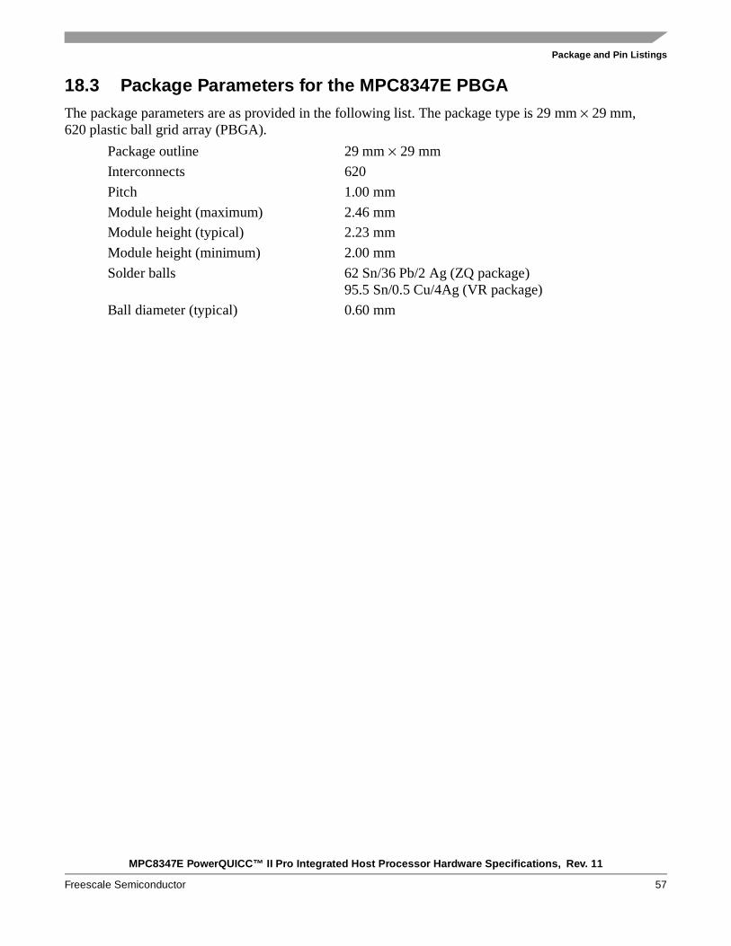
MPC8347E PowerQUICC™ II Pro Integrated Host Processor Hardware Specifications, Rev. 11
Freescale Semiconductor 57
Package and Pin Listings
18.3 Package Parameters for the MPC8347E PBGAThe package parameters are as provided in the following list. The package type is 29 mm × 29 mm, 620 plastic ball grid array (PBGA).
Package outline 29 mm × 29 mm
Interconnects 620
Pitch 1.00 mm
Module height (maximum) 2.46 mm
Module height (typical) 2.23 mm
Module height (minimum) 2.00 mm
Solder balls 62 Sn/36 Pb/2 Ag (ZQ package)95.5 Sn/0.5 Cu/4Ag (VR package)
Ball diameter (typical) 0.60 mm

MPC8347E PowerQUICC™ II Pro Integrated Host Processor Hardware Specifications, Rev. 11
58 Freescale Semiconductor
Package and Pin Listings
18.4 Mechanical Dimensions for the MPC8347E PBGAFigure 40 shows the mechanical dimensions and bottom surface nomenclature for the MPC8347E, 620-PBGA package.
Notes:1.All dimensions are in millimeters.
2.Dimensioning and tolerancing per ASME Y14. 5M-1994.
3.Maximum solder ball diameter measured parallel to datum A.
4.Datum A, the seating plane, is determined by the spherical crowns of the solder balls.
Figure 40. Mechanical Dimensions and Bottom Surface Nomenclature for the MPC8347E PBGA
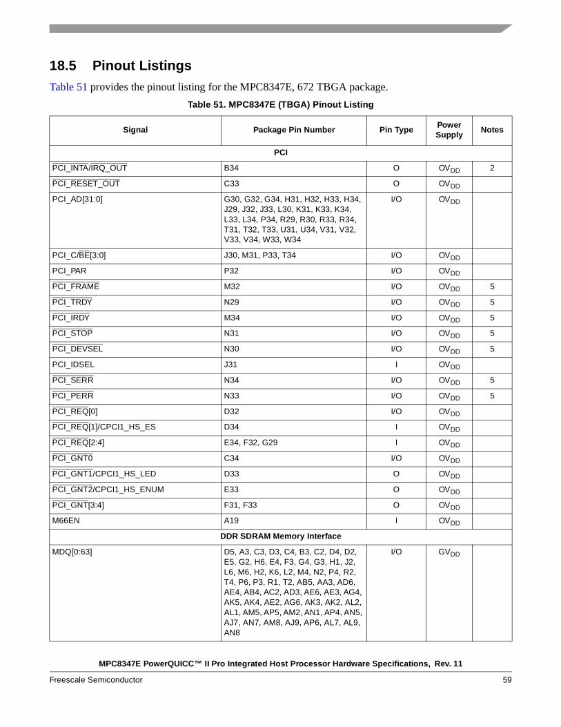
MPC8347E PowerQUICC™ II Pro Integrated Host Processor Hardware Specifications, Rev. 11
Freescale Semiconductor 59
18.5 Pinout ListingsTable 51 provides the pinout listing for the MPC8347E, 672 TBGA package.
Table 51. MPC8347E (TBGA) Pinout Listing
Signal Package Pin Number Pin TypePowerSupply
Notes
PCI
PCI_INTA/IRQ_OUT B34 O OVDD 2
PCI_RESET_OUT C33 O OVDD
PCI_AD[31:0] G30, G32, G34, H31, H32, H33, H34, J29, J32, J33, L30, K31, K33, K34, L33, L34, P34, R29, R30, R33, R34, T31, T32, T33, U31, U34, V31, V32, V33, V34, W33, W34
I/O OVDD
PCI_C/BE[3:0] J30, M31, P33, T34 I/O OVDD
PCI_PAR P32 I/O OVDD
PCI_FRAME M32 I/O OVDD 5
PCI_TRDY N29 I/O OVDD 5
PCI_IRDY M34 I/O OVDD 5
PCI_STOP N31 I/O OVDD 5
PCI_DEVSEL N30 I/O OVDD 5
PCI_IDSEL J31 I OVDD
PCI_SERR N34 I/O OVDD 5
PCI_PERR N33 I/O OVDD 5
PCI_REQ[0] D32 I/O OVDD
PCI_REQ[1]/CPCI1_HS_ES D34 I OVDD
PCI_REQ[2:4] E34, F32, G29 I OVDD
PCI_GNT0 C34 I/O OVDD
PCI_GNT1/CPCI1_HS_LED D33 O OVDD
PCI_GNT2/CPCI1_HS_ENUM E33 O OVDD
PCI_GNT[3:4] F31, F33 O OVDD
M66EN A19 I OVDD
DDR SDRAM Memory Interface
MDQ[0:63] D5, A3, C3, D3, C4, B3, C2, D4, D2, E5, G2, H6, E4, F3, G4, G3, H1, J2, L6, M6, H2, K6, L2, M4, N2, P4, R2, T4, P6, P3, R1, T2, AB5, AA3, AD6, AE4, AB4, AC2, AD3, AE6, AE3, AG4, AK5, AK4, AE2, AG6, AK3, AK2, AL2, AL1, AM5, AP5, AM2, AN1, AP4, AN5, AJ7, AN7, AM8, AJ9, AP6, AL7, AL9, AN8
I/O GVDD
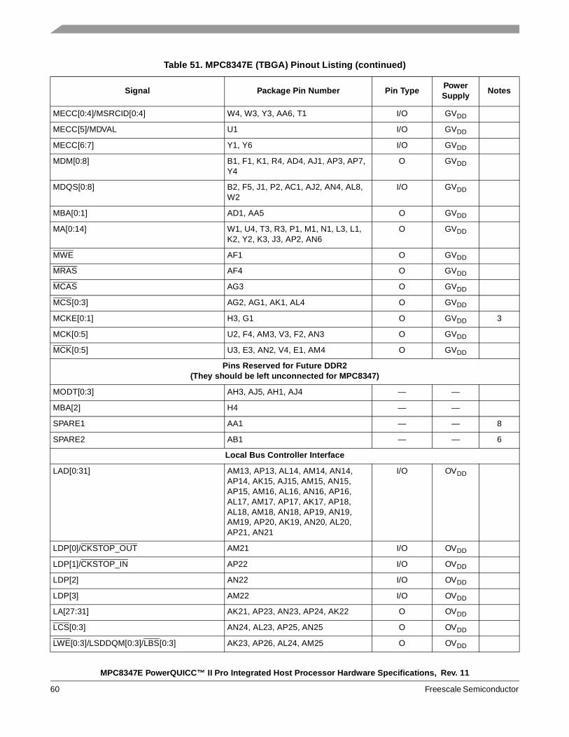
MPC8347E PowerQUICC™ II Pro Integrated Host Processor Hardware Specifications, Rev. 11
60 Freescale Semiconductor
MECC[0:4]/MSRCID[0:4] W4, W3, Y3, AA6, T1 I/O GVDD
MECC[5]/MDVAL U1 I/O GVDD
MECC[6:7] Y1, Y6 I/O GVDD
MDM[0:8] B1, F1, K1, R4, AD4, AJ1, AP3, AP7, Y4
O GVDD
MDQS[0:8] B2, F5, J1, P2, AC1, AJ2, AN4, AL8, W2
I/O GVDD
MBA[0:1] AD1, AA5 O GVDD
MA[0:14] W1, U4, T3, R3, P1, M1, N1, L3, L1, K2, Y2, K3, J3, AP2, AN6
O GVDD
MWE AF1 O GVDD
MRAS AF4 O GVDD
MCAS AG3 O GVDD
MCS[0:3] AG2, AG1, AK1, AL4 O GVDD
MCKE[0:1] H3, G1 O GVDD 3
MCK[0:5] U2, F4, AM3, V3, F2, AN3 O GVDD
MCK[0:5] U3, E3, AN2, V4, E1, AM4 O GVDD
Pins Reserved for Future DDR2(They should be left unconnected for MPC8347)
MODT[0:3] AH3, AJ5, AH1, AJ4 — —
MBA[2] H4 — —
SPARE1 AA1 — — 8
SPARE2 AB1 — — 6
Local Bus Controller Interface
LAD[0:31] AM13, AP13, AL14, AM14, AN14, AP14, AK15, AJ15, AM15, AN15, AP15, AM16, AL16, AN16, AP16, AL17, AM17, AP17, AK17, AP18, AL18, AM18, AN18, AP19, AN19, AM19, AP20, AK19, AN20, AL20, AP21, AN21
I/O OVDD
LDP[0]/CKSTOP_OUT AM21 I/O OVDD
LDP[1]/CKSTOP_IN AP22 I/O OVDD
LDP[2] AN22 I/O OVDD
LDP[3] AM22 I/O OVDD
LA[27:31] AK21, AP23, AN23, AP24, AK22 O OVDD
LCS[0:3] AN24, AL23, AP25, AN25 O OVDD
LWE[0:3]/LSDDQM[0:3]/LBS[0:3] AK23, AP26, AL24, AM25 O OVDD
Table 51. MPC8347E (TBGA) Pinout Listing (continued)
Signal Package Pin Number Pin TypePowerSupply
Notes

MPC8347E PowerQUICC™ II Pro Integrated Host Processor Hardware Specifications, Rev. 11
Freescale Semiconductor 61
LBCTL AN26 O OVDD
LALE AK24 O OVDD
LGPL0/LSDA10/cfg_reset_source0 AP27 I/O OVDD
LGPL1/LSDWE/cfg_reset_source1 AL25 I/O OVDD
LGPL2/LSDRAS/LOE AJ24 O OVDD
LGPL3/LSDCAS/cfg_reset_source2 AN27 I/O OVDD
LGPL4/LGTA/LUPWAIT/LPBSE AP28 I/O OVDD
LGPL5/cfg_clkin_div AL26 I/O OVDD
LCKE AM27 O OVDD
LCLK[0:2] AN28, AK26, AP29 O OVDD
LSYNC_OUT AM12 O OVDD
LSYNC_IN AJ10 I OVDD
General Purpose I/O Timers
GPIO1[0]/GTM1_TIN1/GTM2_TIN2 F24 I/O OVDD
GPIO1[1]/GTM1_TGATE1/GTM2_TGATE2 E24 I/O OVDD
GPIO1[2]/GTM1_TOUT1 B25 I/O OVDD
GPIO1[3]/GTM1_TIN2/GTM2_TIN1 D24 I/O OVDD
GPIO1[4]/GTM1_TGATE2/GTM2_TGATE1 A25 I/O OVDD
GPIO1[5]/GTM1_TOUT2/GTM2_TOUT1 B24 I/O OVDD
GPIO1[6]/GTM1_TIN3/GTM2_TIN4 A24 I/O OVDD
GPIO1[7]/GTM1_TGATE3/GTM2_TGATE4 D23 I/O OVDD
GPIO1[8]/GTM1_TOUT3 B23 I/O OVDD
GPIO1[9]/GTM1_TIN4/GTM2_TIN3 A23 I/O OVDD
GPIO1[10]/GTM1_TGATE4/GTM2_TGATE3 F22 I/O OVDD
GPIO1[11]/GTM1_TOUT4/GTM2_TOUT3 E22 I/O OVDD
USB Port 1
MPH1_D0_ENABLEN/DR_D0_ENABLEN A26 I/O OVDD
MPH1_D1_SER_TXD/DR_D1_SER_TXD B26 I/O OVDD
MPH1_D2_VMO_SE0/DR_D2_VMO_SE0 D25 I/O OVDD
MPH1_D3_SPEED/DR_D3_SPEED A27 I/O OVDD
MPH1_D4_DP/DR_D4_DP B27 I/O OVDD
MPH1_D5_DM/DR_D5_DM C27 I/O OVDD
MPH1_D6_SER_RCV/DR_D6_SER_RCV D26 I/O OVDD
MPH1_D7_DRVVBUS/DR_D7_DRVVBUS E26 I/O OVDD
Table 51. MPC8347E (TBGA) Pinout Listing (continued)
Signal Package Pin Number Pin TypePowerSupply
Notes
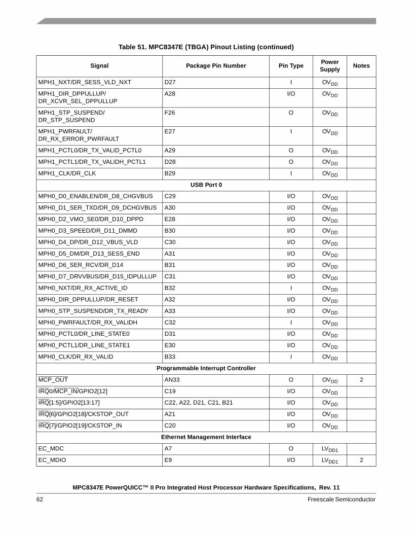
MPC8347E PowerQUICC™ II Pro Integrated Host Processor Hardware Specifications, Rev. 11
62 Freescale Semiconductor
MPH1_NXT/DR_SESS_VLD_NXT D27 I OVDD
MPH1_DIR_DPPULLUP/DR_XCVR_SEL_DPPULLUP
A28 I/O OVDD
MPH1_STP_SUSPEND/DR_STP_SUSPEND
F26 O OVDD
MPH1_PWRFAULT/DR_RX_ERROR_PWRFAULT
E27 I OVDD
MPH1_PCTL0/DR_TX_VALID_PCTL0 A29 O OVDD
MPH1_PCTL1/DR_TX_VALIDH_PCTL1 D28 O OVDD
MPH1_CLK/DR_CLK B29 I OVDD
USB Port 0
MPH0_D0_ENABLEN/DR_D8_CHGVBUS C29 I/O OVDD
MPH0_D1_SER_TXD/DR_D9_DCHGVBUS A30 I/O OVDD
MPH0_D2_VMO_SE0/DR_D10_DPPD E28 I/O OVDD
MPH0_D3_SPEED/DR_D11_DMMD B30 I/O OVDD
MPH0_D4_DP/DR_D12_VBUS_VLD C30 I/O OVDD
MPH0_D5_DM/DR_D13_SESS_END A31 I/O OVDD
MPH0_D6_SER_RCV/DR_D14 B31 I/O OVDD
MPH0_D7_DRVVBUS/DR_D15_IDPULLUP C31 I/O OVDD
MPH0_NXT/DR_RX_ACTIVE_ID B32 I OVDD
MPH0_DIR_DPPULLUP/DR_RESET A32 I/O OVDD
MPH0_STP_SUSPEND/DR_TX_READY A33 I/O OVDD
MPH0_PWRFAULT/DR_RX_VALIDH C32 I OVDD
MPH0_PCTL0/DR_LINE_STATE0 D31 I/O OVDD
MPH0_PCTL1/DR_LINE_STATE1 E30 I/O OVDD
MPH0_CLK/DR_RX_VALID B33 I OVDD
Programmable Interrupt Controller
MCP_OUT AN33 O OVDD 2
IRQ0/MCP_IN/GPIO2[12] C19 I/O OVDD
IRQ[1:5]/GPIO2[13:17] C22, A22, D21, C21, B21 I/O OVDD
IRQ[6]/GPIO2[18]/CKSTOP_OUT A21 I/O OVDD
IRQ[7]/GPIO2[19]/CKSTOP_IN C20 I/O OVDD
Ethernet Management Interface
EC_MDC A7 O LVDD1
EC_MDIO E9 I/O LVDD1 2
Table 51. MPC8347E (TBGA) Pinout Listing (continued)
Signal Package Pin Number Pin TypePowerSupply
Notes
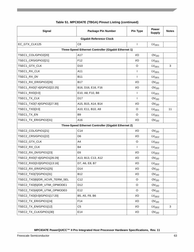
MPC8347E PowerQUICC™ II Pro Integrated Host Processor Hardware Specifications, Rev. 11
Freescale Semiconductor 63
Gigabit Reference Clock
EC_GTX_CLK125 C8 I LVDD1
Three-Speed Ethernet Controller (Gigabit Ethernet 1)
TSEC1_COL/GPIO2[20] A17 I/O OVDD
TSEC1_CRS/GPIO2[21] F12 I/O LVDD1
TSEC1_GTX_CLK D10 O LVDD1 3
TSEC1_RX_CLK A11 I LVDD1
TSEC1_RX_DV B11 I LVDD1
TSEC1_RX_ER/GPIO2[26] B17 I/O OVDD
TSEC1_RXD[7:4]/GPIO2[22:25] B16, D16, E16, F16 I/O OVDD
TSEC1_RXD[3:0] E10, A8, F10, B8 I LVDD1
TSEC1_TX_CLK D17 I OVDD
TSEC1_TXD[7:4]/GPIO2[27:30] A15, B15, A14, B14 I/O OVDD
TSEC1_TXD[3:0] A10, E11, B10, A9 O LVDD1 11
TSEC1_TX_EN B9 O LVDD1
TSEC1_TX_ER/GPIO2[31] A16 I/O OVDD
Three-Speed Ethernet Controller (Gigabit Ethernet 2)
TSEC2_COL/GPIO1[21] C14 I/O OVDD
TSEC2_CRS/GPIO1[22] D6 I/O LVDD2
TSEC2_GTX_CLK A4 O LVDD2
TSEC2_RX_CLK B4 I LVDD2
TSEC2_RX_DV/GPIO1[23] E6 I/O LVDD2
TSEC2_RXD[7:4]/GPIO1[26:29] A13, B13, C13, A12 I/O OVDD
TSEC2_RXD[3:0]/GPIO1[13:16] D7, A6, E8, B7 I/O LVDD2
TSEC2_RX_ER/GPIO1[25] D14 I/O OVDD
TSEC2_TXD[7]/GPIO1[31] B12 I/O OVDD
TSEC2_TXD[6]/DR_XCVR_TERM_SEL C12 O OVDD
TSEC2_TXD[5]/DR_UTMI_OPMODE1 D12 O OVDD
TSEC2_TXD[4]/DR_UTMI_OPMODE0 E12 O OVDD
TSEC2_TXD[3:0]/GPIO1[17:20] B5, A5, F8, B6 I/O LVDD2
TSEC2_TX_ER/GPIO1[24] F14 I/O OVDD
TSEC2_TX_EN/GPIO1[12] C5 I/O LVDD2 3
TSEC2_TX_CLK/GPIO1[30] E14 I/O OVDD
Table 51. MPC8347E (TBGA) Pinout Listing (continued)
Signal Package Pin Number Pin TypePowerSupply
Notes
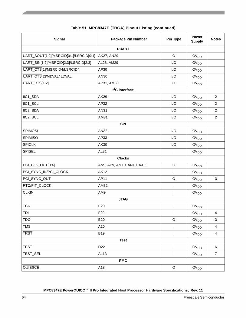
MPC8347E PowerQUICC™ II Pro Integrated Host Processor Hardware Specifications, Rev. 11
64 Freescale Semiconductor
DUART
UART_SOUT[1:2]/MSRCID[0:1]/LSRCID[0:1] AK27, AN29 O OVDD
UART_SIN[1:2]/MSRCID[2:3]/LSRCID[2:3] AL28, AM29 I/O OVDD
UART_CTS[1]/MSRCID4/LSRCID4 AP30 I/O OVDD
UART_CTS[2]/MDVAL/ LDVAL AN30 I/O OVDD
UART_RTS[1:2] AP31, AM30 O OVDD
I2C interface
IIC1_SDA AK29 I/O OVDD 2
IIC1_SCL AP32 I/O OVDD 2
IIC2_SDA AN31 I/O OVDD 2
IIC2_SCL AM31 I/O OVDD 2
SPI
SPIMOSI AN32 I/O OVDD
SPIMISO AP33 I/O OVDD
SPICLK AK30 I/O OVDD
SPISEL AL31 I OVDD
Clocks
PCI_CLK_OUT[0:4] AN9, AP9, AM10, AN10, AJ11 O OVDD
PCI_SYNC_IN/PCI_CLOCK AK12 I OVDD
PCI_SYNC_OUT AP11 O OVDD 3
RTC/PIT_CLOCK AM32 I OVDD
CLKIN AM9 I OVDD
JTAG
TCK E20 I OVDD
TDI F20 I OVDD 4
TDO B20 O OVDD 3
TMS A20 I OVDD 4
TRST B19 I OVDD 4
Test
TEST D22 I OVDD 6
TEST_SEL AL13 I OVDD 7
PMC
QUIESCE A18 O OVDD
Table 51. MPC8347E (TBGA) Pinout Listing (continued)
Signal Package Pin Number Pin TypePowerSupply
Notes
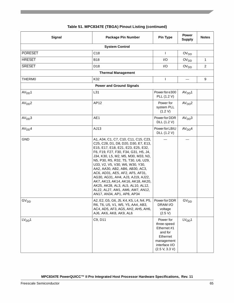
MPC8347E PowerQUICC™ II Pro Integrated Host Processor Hardware Specifications, Rev. 11
Freescale Semiconductor 65
System Control
PORESET C18 I OVDD
HRESET B18 I/O OVDD 1
SRESET D18 I/O OVDD 2
Thermal Management
THERM0 K32 I — 9
Power and Ground Signals
AVDD1 L31 Power for e300 PLL (1.2 V)
AVDD1
AVDD2 AP12 Power for system PLL
(1.2 V)
AVDD2
AVDD3 AE1 Power for DDR DLL (1.2 V)
AVDD3
AVDD4 AJ13 Power for LBIU DLL (1.2 V)
AVDD4
GND A1, A34, C1, C7, C10, C11, C15, C23, C25, C28, D1, D8, D20, D30, E7, E13, E15, E17, E18, E21, E23, E25, E32, F6, F19, F27, F30, F34, G31, H5, J4, J34, K30, L5, M2, M5, M30, M33, N3, N5, P30, R5, R32, T5, T30, U6, U29, U33, V2, V5, V30, W6, W30, Y30, AA2, AA30, AB2, AB6, AB30, AC3, AC6, AD31, AE5, AF2, AF5, AF31, AG30, AG31, AH4, AJ3, AJ19, AJ22, AK7, AK13, AK14, AK16, AK18, AK20, AK25, AK28, AL3, AL5, AL10, AL12, AL22, AL27, AM1, AM6, AM7, AN12, AN17, AN34, AP1, AP8, AP34
— —
GVDD A2, E2, G5, G6, J5, K4, K5, L4, N4, P5, R6, T6, U5, V1, W5, Y5, AA4, AB3, AC4, AD5, AF3, AG5, AH2, AH5, AH6, AJ6, AK6, AK8, AK9, AL6
Power for DDR DRAM I/O
voltage(2.5 V)
GVDD
LVDD1 C9, D11 Power for three-speed Ethernet #1
and for Ethernet
management interface I/O (2.5 V, 3.3 V)
LVDD1
Table 51. MPC8347E (TBGA) Pinout Listing (continued)
Signal Package Pin Number Pin TypePowerSupply
Notes
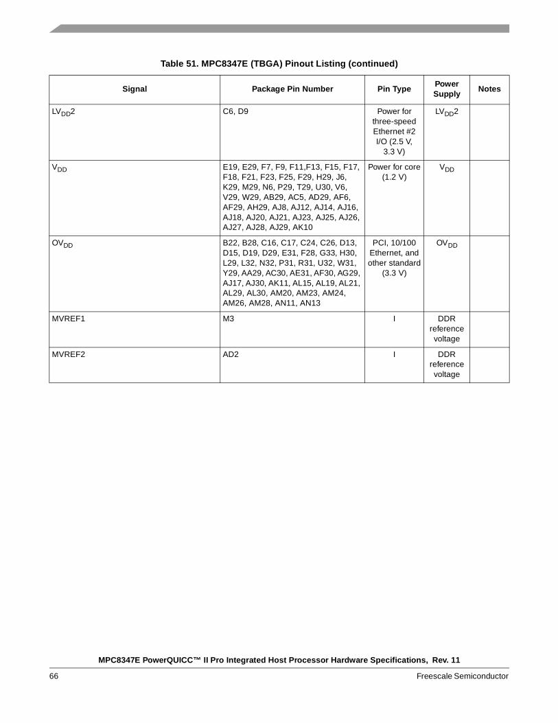
MPC8347E PowerQUICC™ II Pro Integrated Host Processor Hardware Specifications, Rev. 11
66 Freescale Semiconductor
LVDD2 C6, D9 Power for three-speed Ethernet #2 I/O (2.5 V,
3.3 V)
LVDD2
VDD E19, E29, F7, F9, F11,F13, F15, F17, F18, F21, F23, F25, F29, H29, J6, K29, M29, N6, P29, T29, U30, V6, V29, W29, AB29, AC5, AD29, AF6, AF29, AH29, AJ8, AJ12, AJ14, AJ16, AJ18, AJ20, AJ21, AJ23, AJ25, AJ26, AJ27, AJ28, AJ29, AK10
Power for core(1.2 V)
VDD
OVDD B22, B28, C16, C17, C24, C26, D13, D15, D19, D29, E31, F28, G33, H30, L29, L32, N32, P31, R31, U32, W31, Y29, AA29, AC30, AE31, AF30, AG29, AJ17, AJ30, AK11, AL15, AL19, AL21, AL29, AL30, AM20, AM23, AM24, AM26, AM28, AN11, AN13
PCI, 10/100 Ethernet, and other standard
(3.3 V)
OVDD
MVREF1 M3 I DDR reference voltage
MVREF2 AD2 I DDR reference voltage
Table 51. MPC8347E (TBGA) Pinout Listing (continued)
Signal Package Pin Number Pin TypePowerSupply
Notes
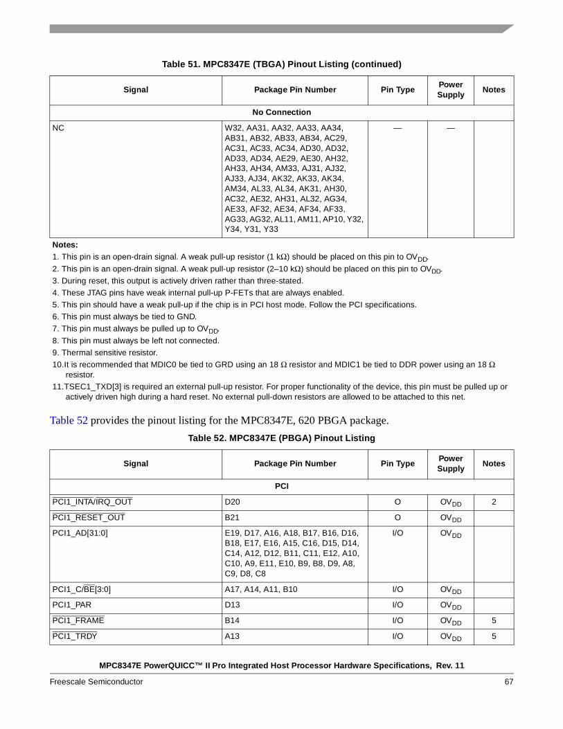
MPC8347E PowerQUICC™ II Pro Integrated Host Processor Hardware Specifications, Rev. 11
Freescale Semiconductor 67
Table 52 provides the pinout listing for the MPC8347E, 620 PBGA package.
No Connection
NC W32, AA31, AA32, AA33, AA34, AB31, AB32, AB33, AB34, AC29, AC31, AC33, AC34, AD30, AD32, AD33, AD34, AE29, AE30, AH32, AH33, AH34, AM33, AJ31, AJ32, AJ33, AJ34, AK32, AK33, AK34, AM34, AL33, AL34, AK31, AH30, AC32, AE32, AH31, AL32, AG34, AE33, AF32, AE34, AF34, AF33, AG33, AG32, AL11, AM11, AP10, Y32, Y34, Y31, Y33
— —
Notes: 1. This pin is an open-drain signal. A weak pull-up resistor (1 kΩ) should be placed on this pin to OVDD.
2. This pin is an open-drain signal. A weak pull-up resistor (2–10 kΩ) should be placed on this pin to OVDD.
3. During reset, this output is actively driven rather than three-stated.
4. These JTAG pins have weak internal pull-up P-FETs that are always enabled.
5. This pin should have a weak pull-up if the chip is in PCI host mode. Follow the PCI specifications.
6. This pin must always be tied to GND.
7. This pin must always be pulled up to OVDD.
8. This pin must always be left not connected.
9. Thermal sensitive resistor.
10.It is recommended that MDIC0 be tied to GRD using an 18 Ω resistor and MDIC1 be tied to DDR power using an 18 Ω resistor.
11.TSEC1_TXD[3] is required an external pull-up resistor. For proper functionality of the device, this pin must be pulled up or actively driven high during a hard reset. No external pull-down resistors are allowed to be attached to this net.
Table 52. MPC8347E (PBGA) Pinout Listing
Signal Package Pin Number Pin TypePowerSupply
Notes
PCI
PCI1_INTA/IRQ_OUT D20 O OVDD 2
PCI1_RESET_OUT B21 O OVDD
PCI1_AD[31:0] E19, D17, A16, A18, B17, B16, D16, B18, E17, E16, A15, C16, D15, D14, C14, A12, D12, B11, C11, E12, A10, C10, A9, E11, E10, B9, B8, D9, A8, C9, D8, C8
I/O OVDD
PCI1_C/BE[3:0] A17, A14, A11, B10 I/O OVDD
PCI1_PAR D13 I/O OVDD
PCI1_FRAME B14 I/O OVDD 5
PCI1_TRDY A13 I/O OVDD 5
Table 51. MPC8347E (TBGA) Pinout Listing (continued)
Signal Package Pin Number Pin TypePowerSupply
Notes
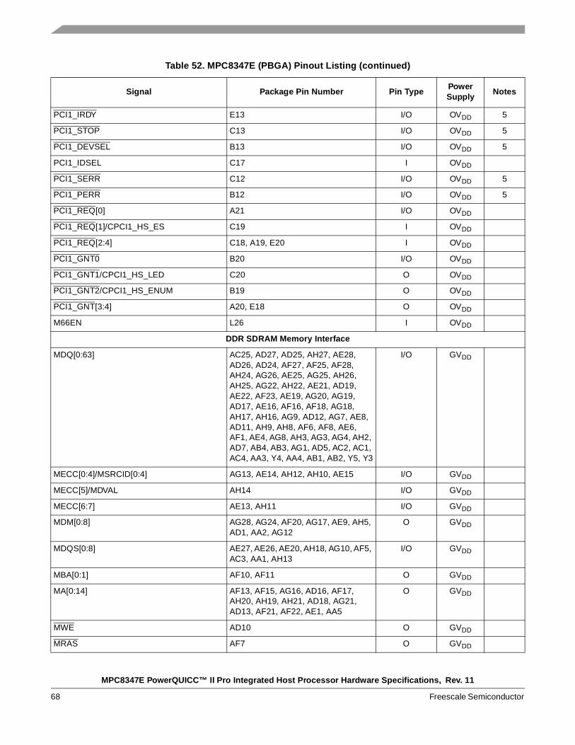
MPC8347E PowerQUICC™ II Pro Integrated Host Processor Hardware Specifications, Rev. 11
68 Freescale Semiconductor
PCI1_IRDY E13 I/O OVDD 5
PCI1_STOP C13 I/O OVDD 5
PCI1_DEVSEL B13 I/O OVDD 5
PCI1_IDSEL C17 I OVDD
PCI1_SERR C12 I/O OVDD 5
PCI1_PERR B12 I/O OVDD 5
PCI1_REQ[0] A21 I/O OVDD
PCI1_REQ[1]/CPCI1_HS_ES C19 I OVDD
PCI1_REQ[2:4] C18, A19, E20 I OVDD
PCI1_GNT0 B20 I/O OVDD
PCI1_GNT1/CPCI1_HS_LED C20 O OVDD
PCI1_GNT2/CPCI1_HS_ENUM B19 O OVDD
PCI1_GNT[3:4] A20, E18 O OVDD
M66EN L26 I OVDD
DDR SDRAM Memory Interface
MDQ[0:63] AC25, AD27, AD25, AH27, AE28, AD26, AD24, AF27, AF25, AF28, AH24, AG26, AE25, AG25, AH26, AH25, AG22, AH22, AE21, AD19, AE22, AF23, AE19, AG20, AG19, AD17, AE16, AF16, AF18, AG18, AH17, AH16, AG9, AD12, AG7, AE8, AD11, AH9, AH8, AF6, AF8, AE6, AF1, AE4, AG8, AH3, AG3, AG4, AH2, AD7, AB4, AB3, AG1, AD5, AC2, AC1, AC4, AA3, Y4, AA4, AB1, AB2, Y5, Y3
I/O GVDD
MECC[0:4]/MSRCID[0:4] AG13, AE14, AH12, AH10, AE15 I/O GVDD
MECC[5]/MDVAL AH14 I/O GVDD
MECC[6:7] AE13, AH11 I/O GVDD
MDM[0:8] AG28, AG24, AF20, AG17, AE9, AH5, AD1, AA2, AG12
O GVDD
MDQS[0:8] AE27, AE26, AE20, AH18, AG10, AF5, AC3, AA1, AH13
I/O GVDD
MBA[0:1] AF10, AF11 O GVDD
MA[0:14] AF13, AF15, AG16, AD16, AF17, AH20, AH19, AH21, AD18, AG21, AD13, AF21, AF22, AE1, AA5
O GVDD
MWE AD10 O GVDD
MRAS AF7 O GVDD
Table 52. MPC8347E (PBGA) Pinout Listing (continued)
Signal Package Pin Number Pin TypePowerSupply
Notes
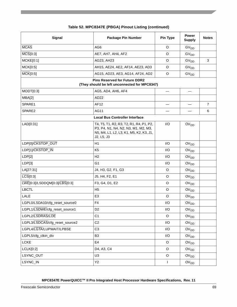
MPC8347E PowerQUICC™ II Pro Integrated Host Processor Hardware Specifications, Rev. 11
Freescale Semiconductor 69
MCAS AG6 O GVDD
MCS[0:3] AE7, AH7, AH4, AF2 O GVDD
MCKE[0:1] AG23, AH23 O GVDD 3
MCK[0:5] AH15, AE24, AE2, AF14, AE23, AD3 O GVDD
MCK[0:5] AG15, AD23, AE3, AG14, AF24, AD2 O GVDD
Pins Reserved for Future DDR2(They should be left unconnected for MPC8347)
MODT[0:3] AG5, AD4, AH6, AF4 — —
MBA[2] AD22
SPARE1 AF12 — — 7
SPARE2 AG11 — — 6
Local Bus Controller Interface
LAD[0:31] T4, T5, T1, R2, R3, T2, R1, R4, P1, P2, P3, P4, N1, N4, N2, N3, M1, M2, M3, N5, M4, L1, L2, L3, K1, M5, K2, K3, J1, J2, L5, J3
I/O OVDD
LDP[0]/CKSTOP_OUT H1 I/O OVDD
LDP[1]/CKSTOP_IN K5 I/O OVDD
LDP[2] H2 I/O OVDD
LDP[3] G1 I/O OVDD
LA[27:31] J4, H3, G2, F1, G3 O OVDD
LCS[0:3] J5, H4, F2, E1 O OVDD
LWE[0:3]/LSDDQM[0:3]/LBS[0:3] F3, G4, D1, E2 O OVDD
LBCTL H5 O OVDD
LALE E3 O OVDD
LGPL0/LSDA10/cfg_reset_source0 F4 I/O OVDD
LGPL1/LSDWE/cfg_reset_source1 D2 I/O OVDD
LGPL2/LSDRAS/LOE C1 O OVDD
LGPL3/LSDCAS/cfg_reset_source2 C2 I/O OVDD
LGPL4/LGTA/LUPWAIT/LPBSE C3 I/O OVDD
LGPL5/cfg_clkin_div B3 I/O OVDD
LCKE E4 O OVDD
LCLK[0:2] D4, A3, C4 O OVDD
LSYNC_OUT U3 O OVDD
LSYNC_IN Y2 I OVDD
Table 52. MPC8347E (PBGA) Pinout Listing (continued)
Signal Package Pin Number Pin TypePowerSupply
Notes
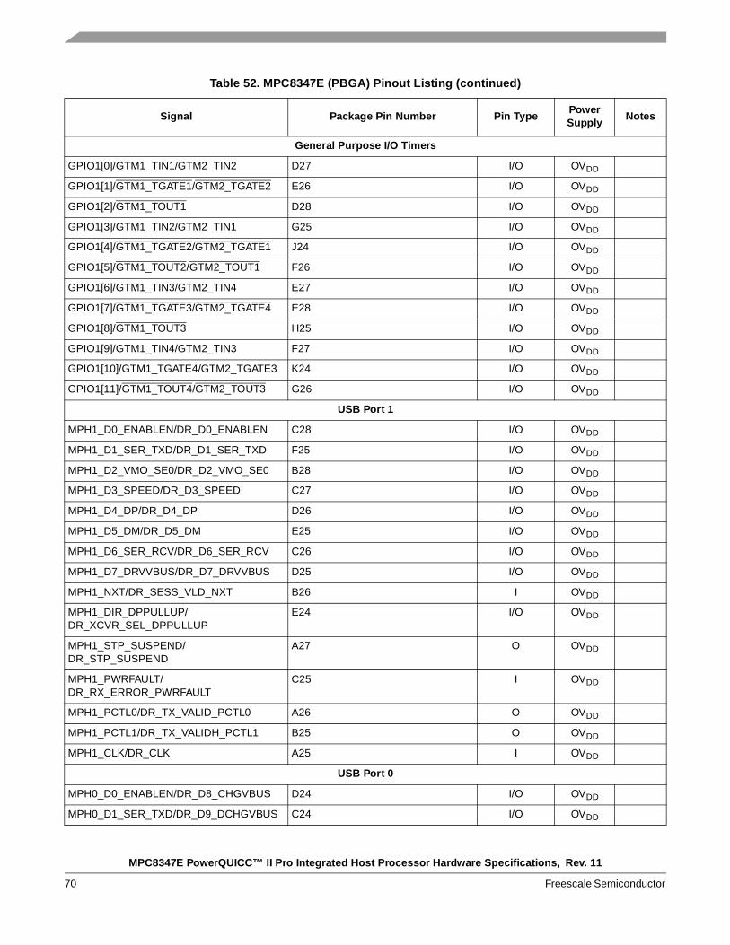
MPC8347E PowerQUICC™ II Pro Integrated Host Processor Hardware Specifications, Rev. 11
70 Freescale Semiconductor
General Purpose I/O Timers
GPIO1[0]/GTM1_TIN1/GTM2_TIN2 D27 I/O OVDD
GPIO1[1]/GTM1_TGATE1/GTM2_TGATE2 E26 I/O OVDD
GPIO1[2]/GTM1_TOUT1 D28 I/O OVDD
GPIO1[3]/GTM1_TIN2/GTM2_TIN1 G25 I/O OVDD
GPIO1[4]/GTM1_TGATE2/GTM2_TGATE1 J24 I/O OVDD
GPIO1[5]/GTM1_TOUT2/GTM2_TOUT1 F26 I/O OVDD
GPIO1[6]/GTM1_TIN3/GTM2_TIN4 E27 I/O OVDD
GPIO1[7]/GTM1_TGATE3/GTM2_TGATE4 E28 I/O OVDD
GPIO1[8]/GTM1_TOUT3 H25 I/O OVDD
GPIO1[9]/GTM1_TIN4/GTM2_TIN3 F27 I/O OVDD
GPIO1[10]/GTM1_TGATE4/GTM2_TGATE3 K24 I/O OVDD
GPIO1[11]/GTM1_TOUT4/GTM2_TOUT3 G26 I/O OVDD
USB Port 1
MPH1_D0_ENABLEN/DR_D0_ENABLEN C28 I/O OVDD
MPH1_D1_SER_TXD/DR_D1_SER_TXD F25 I/O OVDD
MPH1_D2_VMO_SE0/DR_D2_VMO_SE0 B28 I/O OVDD
MPH1_D3_SPEED/DR_D3_SPEED C27 I/O OVDD
MPH1_D4_DP/DR_D4_DP D26 I/O OVDD
MPH1_D5_DM/DR_D5_DM E25 I/O OVDD
MPH1_D6_SER_RCV/DR_D6_SER_RCV C26 I/O OVDD
MPH1_D7_DRVVBUS/DR_D7_DRVVBUS D25 I/O OVDD
MPH1_NXT/DR_SESS_VLD_NXT B26 I OVDD
MPH1_DIR_DPPULLUP/DR_XCVR_SEL_DPPULLUP
E24 I/O OVDD
MPH1_STP_SUSPEND/DR_STP_SUSPEND
A27 O OVDD
MPH1_PWRFAULT/DR_RX_ERROR_PWRFAULT
C25 I OVDD
MPH1_PCTL0/DR_TX_VALID_PCTL0 A26 O OVDD
MPH1_PCTL1/DR_TX_VALIDH_PCTL1 B25 O OVDD
MPH1_CLK/DR_CLK A25 I OVDD
USB Port 0
MPH0_D0_ENABLEN/DR_D8_CHGVBUS D24 I/O OVDD
MPH0_D1_SER_TXD/DR_D9_DCHGVBUS C24 I/O OVDD
Table 52. MPC8347E (PBGA) Pinout Listing (continued)
Signal Package Pin Number Pin TypePowerSupply
Notes
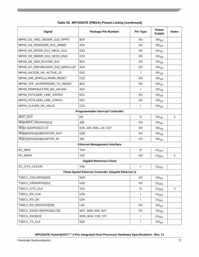
MPC8347E PowerQUICC™ II Pro Integrated Host Processor Hardware Specifications, Rev. 11
Freescale Semiconductor 71
MPH0_D2_VMO_SE0/DR_D10_DPPD B24 I/O OVDD
MPH0_D3_SPEED/DR_D11_DMMD A24 I/O OVDD
MPH0_D4_DP/DR_D12_VBUS_VLD D23 I/O OVDD
MPH0_D5_DM/DR_D13_SESS_END C23 I/O OVDD
MPH0_D6_SER_RCV/DR_D14 B23 I/O OVDD
MPH0_D7_DRVVBUS/DR_D15_IDPULLUP A23 I/O OVDD
MPH0_NXT/DR_RX_ACTIVE_ID D22 I OVDD
MPH0_DIR_DPPULLUP/DR_RESET C22 I/O OVDD
MPH0_STP_SUSPEND/DR_TX_READY B22 I/O OVDD
MPH0_PWRFAULT/DR_RX_VALIDH A22 I OVDD
MPH0_PCTL0/DR_LINE_STATE0 E21 I/O OVDD
MPH0_PCTL1/DR_LINE_STATE1 D21 I/O OVDD
MPH0_CLK/DR_RX_VALID C21 I OVDD
Programmable Interrupt Controller
MCP_OUT E8 O OVDD 2
IRQ0/MCP_IN/GPIO2[12] J28 I/O OVDD
IRQ[1:5]/GPIO2[13:17] K25, J25, H26, L24, G27 I/O OVDD
IRQ[6]/GPIO2[18]/CKSTOP_OUT G28 I/O OVDD
IRQ[7]/GPIO2[19]/CKSTOP_IN J26 I/O OVDD
Ethernet Management Interface
EC_MDC Y24 O LVDD1
EC_MDIO Y25 I/O LVDD1 2
Gigabit Reference Clock
EC_GTX_CLK125 Y26 I LVDD1
Three-Speed Ethernet Controller (Gigabit Ethernet 1)
TSEC1_COL/GPIO2[20] M26 I/O OVDD
TSEC1_CRS/GPIO2[21] U25 I/O LVDD1
TSEC1_GTX_CLK V24 O LVDD1 3
TSEC1_RX_CLK U26 I LVDD1
TSEC1_RX_DV U24 I LVDD1
TSEC1_RX_ER/GPIO2[26] L28 I/O OVDD
TSEC1_RXD[7:4]/GPIO2[22:25] M27, M28, N26, N27 I/O OVDD
TSEC1_RXD[3:0] W26, W24, Y28, Y27 I LVDD1
TSEC1_TX_CLK N25 I OVDD
Table 52. MPC8347E (PBGA) Pinout Listing (continued)
Signal Package Pin Number Pin TypePowerSupply
Notes
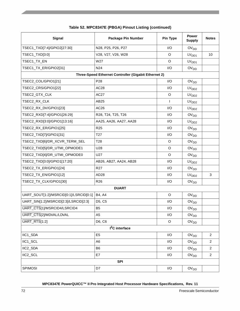
MPC8347E PowerQUICC™ II Pro Integrated Host Processor Hardware Specifications, Rev. 11
72 Freescale Semiconductor
TSEC1_TXD[7:4]/GPIO2[27:30] N28, P25, P26, P27 I/O OVDD
TSEC1_TXD[3:0] V28, V27, V26, W28 O LVDD1 10
TSEC1_TX_EN W27 O LVDD1
TSEC1_TX_ER/GPIO2[31] N24 I/O OVDD
Three-Speed Ethernet Controller (Gigabit Ethernet 2)
TSEC2_COL/GPIO1[21] P28 I/O OVDD
TSEC2_CRS/GPIO1[22] AC28 I/O LVDD2
TSEC2_GTX_CLK AC27 O LVDD2
TSEC2_RX_CLK AB25 I LVDD2
TSEC2_RX_DV/GPIO1[23] AC26 I/O LVDD2
TSEC2_RXD[7:4]/GPIO1[26:29] R28, T24, T25, T26 I/O OVDD
TSEC2_RXD[3:0]/GPIO1[13:16] AA25, AA26, AA27, AA28 I/O LVDD2
TSEC2_RX_ER/GPIO1[25] R25 I/O OVDD
TSEC2_TXD[7]/GPIO1[31] T27 I/O OVDD
TSEC2_TXD[6]/DR_XCVR_TERM_SEL T28 O OVDD
TSEC2_TXD[5]/DR_UTMI_OPMODE1 U28 O OVDD
TSEC2_TXD[4]/DR_UTMI_OPMODE0 U27 O OVDD
TSEC2_TXD[3:0]/GPIO1[17:20] AB26, AB27, AA24, AB28 I/O LVDD2
TSEC2_TX_ER/GPIO1[24] R27 I/O OVDD
TSEC2_TX_EN/GPIO1[12] AD28 I/O LVDD2 3
TSEC2_TX_CLK/GPIO1[30] R26 I/O OVDD
DUART
UART_SOUT[1:2]/MSRCID[0:1]/LSRCID[0:1] B4, A4 O OVDD
UART_SIN[1:2]/MSRCID[2:3]/LSRCID[2:3] D5, C5 I/O OVDD
UART_CTS[1]/MSRCID4/LSRCID4 B5 I/O OVDD
UART_CTS[2]/MDVAL/LDVAL A5 I/O OVDD
UART_RTS[1:2] D6, C6 O OVDD
I2C interface
IIC1_SDA E5 I/O OVDD 2
IIC1_SCL A6 I/O OVDD 2
IIC2_SDA B6 I/O OVDD 2
IIC2_SCL E7 I/O OVDD 2
SPI
SPIMOSI D7 I/O OVDD
Table 52. MPC8347E (PBGA) Pinout Listing (continued)
Signal Package Pin Number Pin TypePowerSupply
Notes
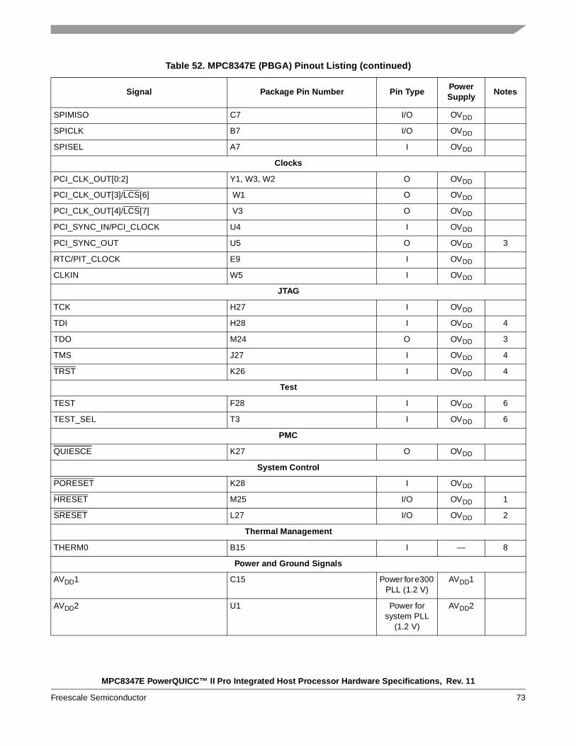
MPC8347E PowerQUICC™ II Pro Integrated Host Processor Hardware Specifications, Rev. 11
Freescale Semiconductor 73
SPIMISO C7 I/O OVDD
SPICLK B7 I/O OVDD
SPISEL A7 I OVDD
Clocks
PCI_CLK_OUT[0:2] Y1, W3, W2 O OVDD
PCI_CLK_OUT[3]/LCS[6] W1 O OVDD
PCI_CLK_OUT[4]/LCS[7] V3 O OVDD
PCI_SYNC_IN/PCI_CLOCK U4 I OVDD
PCI_SYNC_OUT U5 O OVDD 3
RTC/PIT_CLOCK E9 I OVDD
CLKIN W5 I OVDD
JTAG
TCK H27 I OVDD
TDI H28 I OVDD 4
TDO M24 O OVDD 3
TMS J27 I OVDD 4
TRST K26 I OVDD 4
Test
TEST F28 I OVDD 6
TEST_SEL T3 I OVDD 6
PMC
QUIESCE K27 O OVDD
System Control
PORESET K28 I OVDD
HRESET M25 I/O OVDD 1
SRESET L27 I/O OVDD 2
Thermal Management
THERM0 B15 I — 8
Power and Ground Signals
AVDD1 C15 Power for e300 PLL (1.2 V)
AVDD1
AVDD2 U1 Power for system PLL
(1.2 V)
AVDD2
Table 52. MPC8347E (PBGA) Pinout Listing (continued)
Signal Package Pin Number Pin TypePowerSupply
Notes
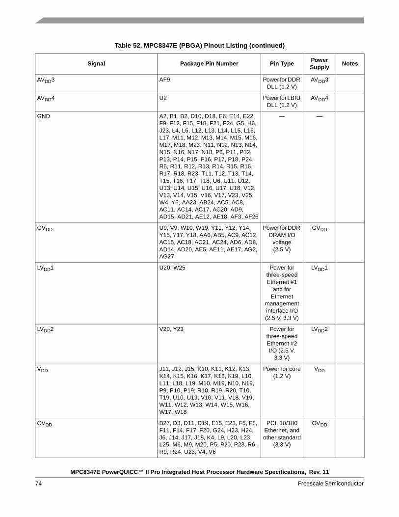
MPC8347E PowerQUICC™ II Pro Integrated Host Processor Hardware Specifications, Rev. 11
74 Freescale Semiconductor
AVDD3 AF9 Power for DDR DLL (1.2 V)
AVDD3
AVDD4 U2 Power for LBIU DLL (1.2 V)
AVDD4
GND A2, B1, B2, D10, D18, E6, E14, E22, F9, F12, F15, F18, F21, F24, G5, H6, J23, L4, L6, L12, L13, L14, L15, L16, L17, M11, M12, M13, M14, M15, M16, M17, M18, M23, N11, N12, N13, N14, N15, N16, N17, N18, P6, P11, P12, P13, P14, P15, P16, P17, P18, P24, R5, R11, R12, R13, R14, R15, R16, R17, R18, R23, T11, T12, T13, T14, T15, T16, T17, T18, U6, U11, U12, U13, U14, U15, U16, U17, U18, V12, V13, V14, V15, V16, V17, V23, V25, W4, Y6, AA23, AB24, AC5, AC8, AC11, AC14, AC17, AC20, AD9, AD15, AD21, AE12, AE18, AF3, AF26
— —
GVDD U9, V9, W10, W19, Y11, Y12, Y14, Y15, Y17, Y18, AA6, AB5, AC9, AC12, AC15, AC18, AC21, AC24, AD6, AD8, AD14, AD20, AE5, AE11, AE17, AG2, AG27
Power for DDR DRAM I/O
voltage(2.5 V)
GVDD
LVDD1 U20, W25 Power for three-speed Ethernet #1
and for Ethernet
management interface I/O (2.5 V, 3.3 V)
LVDD1
LVDD2 V20, Y23 Power for three-speed Ethernet #2 I/O (2.5 V,
3.3 V)
LVDD2
VDD J11, J12, J15, K10, K11, K12, K13, K14, K15, K16, K17, K18, K19, L10, L11, L18, L19, M10, M19, N10, N19, P9, P10, P19, R10, R19, R20, T10, T19, U10, U19, V10, V11, V18, V19, W11, W12, W13, W14, W15, W16, W17, W18
Power for core(1.2 V)
VDD
OVDD B27, D3, D11, D19, E15, E23, F5, F8, F11, F14, F17, F20, G24, H23, H24, J6, J14, J17, J18, K4, L9, L20, L23, L25, M6, M9, M20, P5, P20, P23, R6, R9, R24, U23, V4, V6
PCI, 10/100 Ethernet, and other standard
(3.3 V)
OVDD
Table 52. MPC8347E (PBGA) Pinout Listing (continued)
Signal Package Pin Number Pin TypePowerSupply
Notes
MPC8347E PowerQUICC™ II Pro Integrated Host Processor Hardware Specifications, Rev. 11
Freescale Semiconductor 75
MVREF1 AF19 I DDR reference voltage
MVREF2 AE10 I DDR reference voltage
No Connection
NC V1, V2, V5
Notes: 1. This pin is an open-drain signal. A weak pull-up resistor (1 kΩ) should be placed on this pin to OVDD.
2. This pin is an open-drain signal. A weak pull-up resistor (2–10 kΩ) should be placed on this pin to OVDD.
3. During reset, this output is actively driven rather than three-stated.
4. These JTAG pins have weak internal pull-up P-FETs that are always enabled.
5. This pin should have a weak pull-up if the chip is in PCI host mode. Follow the PCI specifications.
6. This pin must always be tied to GND.
7. This pin must always be left not connected.
8. Thermal sensitive resistor.
9. It is recommended that MDIC0 be tied to GRD using an 18 Ω resistor and MDIC1 be tied to DDR power using an 18 Ω resistor.
10.TSEC1_TXD[3] is required an external pull-up resistor. For proper functionality of the device, this pin must be pulled up or actively driven high during a hard reset. No external pull-down resistors are allowed to be attached to this net.
Table 52. MPC8347E (PBGA) Pinout Listing (continued)
Signal Package Pin Number Pin TypePowerSupply
Notes
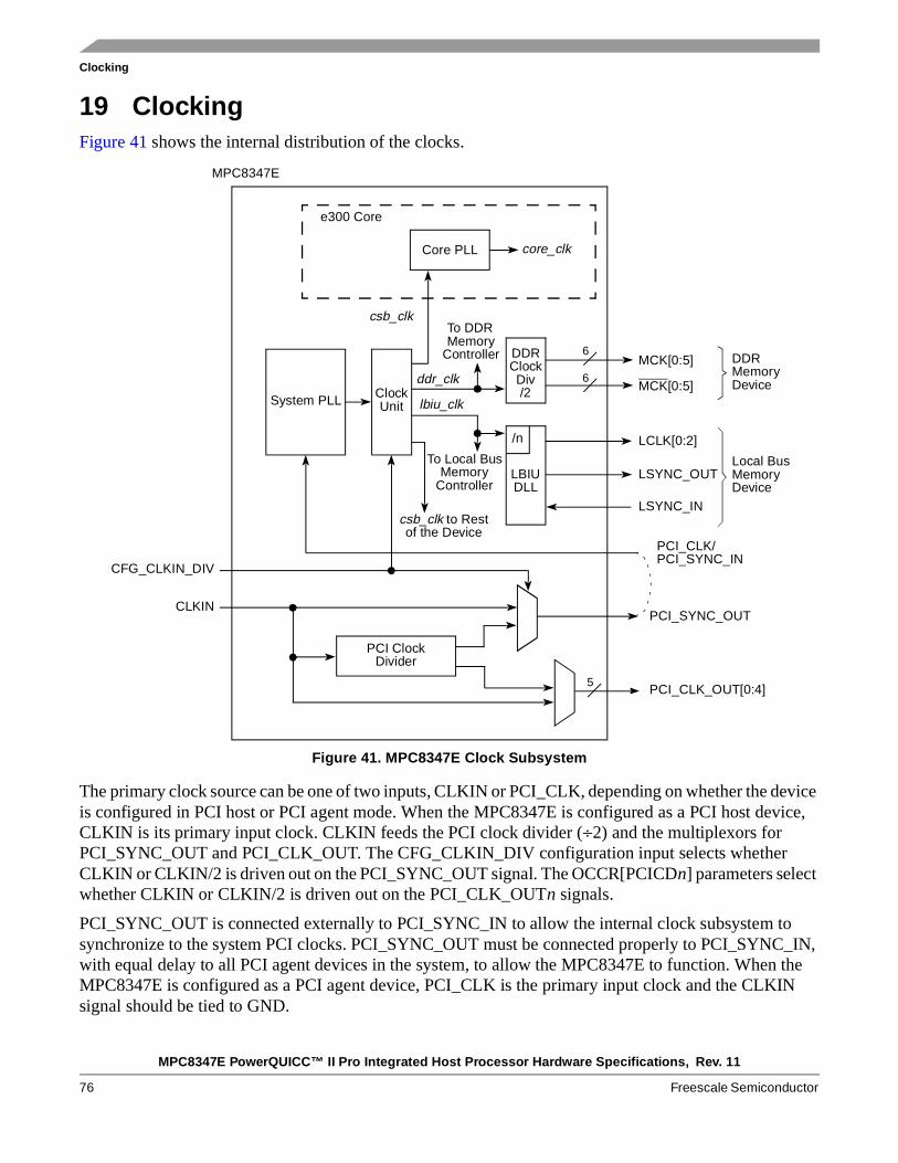
MPC8347E PowerQUICC™ II Pro Integrated Host Processor Hardware Specifications, Rev. 11
76 Freescale Semiconductor
Clocking
19 ClockingFigure 41 shows the internal distribution of the clocks.
Figure 41. MPC8347E Clock Subsystem
The primary clock source can be one of two inputs, CLKIN or PCI_CLK, depending on whether the device is configured in PCI host or PCI agent mode. When the MPC8347E is configured as a PCI host device, CLKIN is its primary input clock. CLKIN feeds the PCI clock divider (÷2) and the multiplexors for PCI_SYNC_OUT and PCI_CLK_OUT. The CFG_CLKIN_DIV configuration input selects whether CLKIN or CLKIN/2 is driven out on the PCI_SYNC_OUT signal. The OCCR[PCICDn] parameters select whether CLKIN or CLKIN/2 is driven out on the PCI_CLK_OUTn signals.
PCI_SYNC_OUT is connected externally to PCI_SYNC_IN to allow the internal clock subsystem to synchronize to the system PCI clocks. PCI_SYNC_OUT must be connected properly to PCI_SYNC_IN, with equal delay to all PCI agent devices in the system, to allow the MPC8347E to function. When the MPC8347E is configured as a PCI agent device, PCI_CLK is the primary input clock and the CLKIN signal should be tied to GND.
Core PLL
System PLL
DDR
LBIU
LSYNC_IN
LSYNC_OUT
LCLK[0:2]
MCK[0:5]
MCK[0:5]
core_clk
e300 Core
csb_clk to Rest
CLKIN
csb_clk
MPC8347E
6
6
DDRMemory
Local Bus
PCI_CLK_OUT[0:4]
PCI_SYNC_OUT
PCI_CLK/
ClockUnit
of the Device
ddr_clk
lbiu_clk
CFG_CLKIN_DIV
PCI Clock
PCI_SYNC_IN
Device
MemoryDevice
/n
To Local BusMemory
Controller
To DDRMemory
Controller
DLL
ClockDiv/2
Divider
5
MPC8347E PowerQUICC™ II Pro Integrated Host Processor Hardware Specifications, Rev. 11
Freescale Semiconductor 77
Clocking
As shown in Figure 41, the primary clock input (frequency) is multiplied up by the system phase-locked loop (PLL) and the clock unit to create the coherent system bus clock (csb_clk), the internal clock for the DDR controller (ddr_clk), and the internal clock for the local bus interface unit (lbiu_clk).
The csb_clk frequency is derived from a complex set of factors that can be simplified into the following equation:
csb_clk = {PCI_SYNC_IN × (1 + CFG_CLKIN_DIV)} × SPMF
In PCI host mode, PCI_SYNC_IN × (1 + CFG_CLKIN_DIV) is the CLKIN frequency.
The csb_clk serves as the clock input to the e300 core. A second PLL inside the e300 core multiplies the csb_clk frequency to create the internal clock for the e300 core (core_clk). The system and core PLL multipliers are selected by the SPMF and COREPLL fields in the reset configuration word low (RCWL), which is loaded at power-on reset or by one of the hard-coded reset options. See the chapter on reset, clocking, and initialization in the MPC8349E Reference Manual for more information on the clock subsystem.
The internal ddr_clk frequency is determined by the following equation:
ddr_clk = csb_clk × (1 + RCWL[DDRCM])
ddr_clk is not the external memory bus frequency; ddr_clk passes through the DDR clock divider (÷2) to create the differential DDR memory bus clock outputs (MCK and MCK). However, the data rate is the same frequency as ddr_clk.
The internal lbiu_clk frequency is determined by the following equation:
lbiu_clk = csb_clk × (1 + RCWL[LBIUCM])
lbiu_clk is not the external local bus frequency; lbiu_clk passes through the LBIU clock divider to create the external local bus clock outputs (LSYNC_OUT and LCLK[0:2]). The LBIU clock divider ratio is controlled by LCCR[CLKDIV].
In addition, some of the internal units may have to be shut off or operate at lower frequency than the csb_clk frequency. Those units have a default clock ratio that can be configured by a memory-mapped register after the device exits reset. Table 53 specifies which units have a configurable clock frequency.
Table 53. Configurable Clock Units
UnitDefault
FrequencyOptions
TSEC1 csb_clk/3 Off, csb_clk, csb_clk/2, csb_clk/3
TSEC2, I2C1 csb_clk/3 Off, csb_clk, csb_clk/2, csb_clk/3
Security core csb_clk/3 Off, csb_clk, csb_clk/2, csb_clk/3
USB DR, USB MPH csb_clk/3 Off, csb_clk, csb_clk/2, csb_clk/3
PCI and DMA complex csb_clk Off, csb_clk
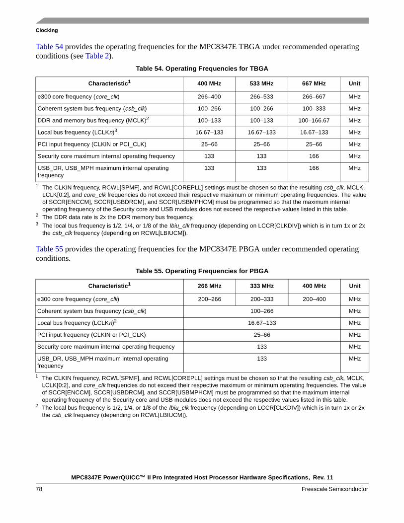
MPC8347E PowerQUICC™ II Pro Integrated Host Processor Hardware Specifications, Rev. 11
78 Freescale Semiconductor
Clocking
Table 54 provides the operating frequencies for the MPC8347E TBGA under recommended operating conditions (see Table 2).
Table 55 provides the operating frequencies for the MPC8347E PBGA under recommended operating conditions.
Table 54. Operating Frequencies for TBGA
Characteristic1
1 The CLKIN frequency, RCWL[SPMF], and RCWL[COREPLL] settings must be chosen so that the resulting csb_clk, MCLK, LCLK[0:2], and core_clk frequencies do not exceed their respective maximum or minimum operating frequencies. The value of SCCR[ENCCM], SCCR[USBDRCM], and SCCR[USBMPHCM] must be programmed so that the maximum internal operating frequency of the Security core and USB modules does not exceed the respective values listed in this table.
400 MHz 533 MHz 667 MHz Unit
e300 core frequency (core_clk) 266–400 266–533 266–667 MHz
Coherent system bus frequency (csb_clk) 100–266 100–266 100–333 MHz
DDR and memory bus frequency (MCLK)2
2 The DDR data rate is 2x the DDR memory bus frequency.
100–133 100–133 100–166.67 MHz
Local bus frequency (LCLKn)3
3 The local bus frequency is 1/2, 1/4, or 1/8 of the lbiu_clk frequency (depending on LCCR[CLKDIV]) which is in turn 1x or 2x the csb_clk frequency (depending on RCWL[LBIUCM]).
16.67–133 16.67–133 16.67–133 MHz
PCI input frequency (CLKIN or PCI_CLK) 25–66 25–66 25–66 MHz
Security core maximum internal operating frequency 133 133 166 MHz
USB_DR, USB_MPH maximum internal operating frequency
133 133 166 MHz
Table 55. Operating Frequencies for PBGA
Characteristic1
1 The CLKIN frequency, RCWL[SPMF], and RCWL[COREPLL] settings must be chosen so that the resulting csb_clk, MCLK, LCLK[0:2], and core_clk frequencies do not exceed their respective maximum or minimum operating frequencies. The value of SCCR[ENCCM], SCCR[USBDRCM], and SCCR[USBMPHCM] must be programmed so that the maximum internal operating frequency of the Security core and USB modules does not exceed the respective values listed in this table.
266 MHz 333 MHz 400 MHz Unit
e300 core frequency (core_clk) 200–266 200–333 200–400 MHz
Coherent system bus frequency (csb_clk) 100–266 MHz
Local bus frequency (LCLKn)2
2 The local bus frequency is 1/2, 1/4, or 1/8 of the lbiu_clk frequency (depending on LCCR[CLKDIV]) which is in turn 1x or 2x the csb_clk frequency (depending on RCWL[LBIUCM]).
16.67–133 MHz
PCI input frequency (CLKIN or PCI_CLK) 25–66 MHz
Security core maximum internal operating frequency 133 MHz
USB_DR, USB_MPH maximum internal operating frequency
133 MHz
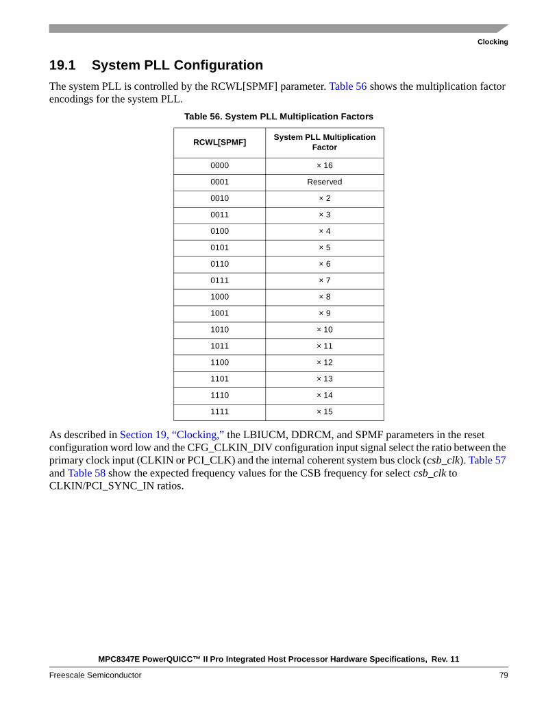
MPC8347E PowerQUICC™ II Pro Integrated Host Processor Hardware Specifications, Rev. 11
Freescale Semiconductor 79
Clocking
19.1 System PLL Configuration The system PLL is controlled by the RCWL[SPMF] parameter. Table 56 shows the multiplication factor encodings for the system PLL.
As described in Section 19, “Clocking,” the LBIUCM, DDRCM, and SPMF parameters in the reset configuration word low and the CFG_CLKIN_DIV configuration input signal select the ratio between the primary clock input (CLKIN or PCI_CLK) and the internal coherent system bus clock (csb_clk). Table 57 and Table 58 show the expected frequency values for the CSB frequency for select csb_clk to CLKIN/PCI_SYNC_IN ratios.
Table 56. System PLL Multiplication Factors
RCWL[SPMF]System PLL Multiplication
Factor
0000 × 16
0001 Reserved
0010 × 2
0011 × 3
0100 × 4
0101 × 5
0110 × 6
0111 × 7
1000 × 8
1001 × 9
1010 × 10
1011 × 11
1100 × 12
1101 × 13
1110 × 14
1111 × 15
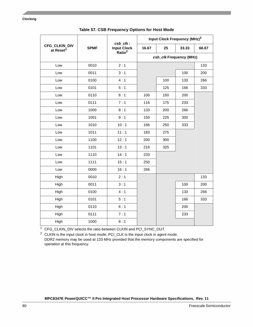
MPC8347E PowerQUICC™ II Pro Integrated Host Processor Hardware Specifications, Rev. 11
80 Freescale Semiconductor
Clocking
Table 57. CSB Frequency Options for Host Mode
CFG_CLKIN_DIV at Reset1
1 CFG_CLKIN_DIV selects the ratio between CLKIN and PCI_SYNC_OUT.
SPMFcsb_clk :
Input Clock Ratio2
2 CLKIN is the input clock in host mode; PCI_CLK is the input clock in agent mode. DDR2 memory may be used at 133 MHz provided that the memory components are specified for operation at this frequency.
Input Clock Frequency (MHz)2
16.67 25 33.33 66.67
csb_clk Frequency (MHz)
Low 0010 2 : 1 133
Low 0011 3 : 1 100 200
Low 0100 4 : 1 100 133 266
Low 0101 5 : 1 125 166 333
Low 0110 6 : 1 100 150 200
Low 0111 7 : 1 116 175 233
Low 1000 8 : 1 133 200 266
Low 1001 9 : 1 150 225 300
Low 1010 10 : 1 166 250 333
Low 1011 11 : 1 183 275
Low 1100 12 : 1 200 300
Low 1101 13 : 1 216 325
Low 1110 14 : 1 233
Low 1111 15 : 1 250
Low 0000 16 : 1 266
High 0010 2 : 1 133
High 0011 3 : 1 100 200
High 0100 4 : 1 133 266
High 0101 5 : 1 166 333
High 0110 6 : 1 200
High 0111 7 : 1 233
High 1000 8 : 1
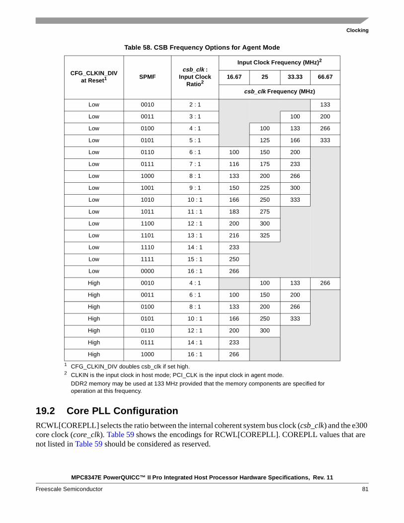
MPC8347E PowerQUICC™ II Pro Integrated Host Processor Hardware Specifications, Rev. 11
Freescale Semiconductor 81
Clocking
19.2 Core PLL ConfigurationRCWL[COREPLL] selects the ratio between the internal coherent system bus clock (csb_clk) and the e300 core clock (core_clk). Table 59 shows the encodings for RCWL[COREPLL]. COREPLL values that are not listed in Table 59 should be considered as reserved.
Table 58. CSB Frequency Options for Agent Mode
CFG_CLKIN_DIV at Reset1
1 CFG_CLKIN_DIV doubles csb_clk if set high.
SPMFcsb_clk :
Input Clock Ratio2
2 CLKIN is the input clock in host mode; PCI_CLK is the input clock in agent mode.
DDR2 memory may be used at 133 MHz provided that the memory components are specified for operation at this frequency.
Input Clock Frequency (MHz)2
16.67 25 33.33 66.67
csb_clk Frequency (MHz)
Low 0010 2 : 1 133
Low 0011 3 : 1 100 200
Low 0100 4 : 1 100 133 266
Low 0101 5 : 1 125 166 333
Low 0110 6 : 1 100 150 200
Low 0111 7 : 1 116 175 233
Low 1000 8 : 1 133 200 266
Low 1001 9 : 1 150 225 300
Low 1010 10 : 1 166 250 333
Low 1011 11 : 1 183 275
Low 1100 12 : 1 200 300
Low 1101 13 : 1 216 325
Low 1110 14 : 1 233
Low 1111 15 : 1 250
Low 0000 16 : 1 266
High 0010 4 : 1 100 133 266
High 0011 6 : 1 100 150 200
High 0100 8 : 1 133 200 266
High 0101 10 : 1 166 250 333
High 0110 12 : 1 200 300
High 0111 14 : 1 233
High 1000 16 : 1 266
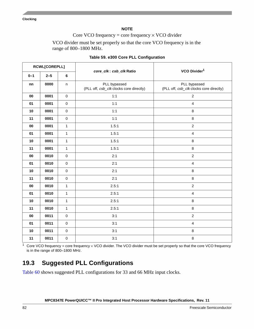
MPC8347E PowerQUICC™ II Pro Integrated Host Processor Hardware Specifications, Rev. 11
82 Freescale Semiconductor
Clocking
NOTE
Core VCO frequency = core frequency × VCO divider
VCO divider must be set properly so that the core VCO frequency is in the range of 800–1800 MHz.
19.3 Suggested PLL ConfigurationsTable 60 shows suggested PLL configurations for 33 and 66 MHz input clocks.
Table 59. e300 Core PLL Configuration
RCWL[COREPLL]core_clk : csb_clk Ratio VCO Divider1
1 Core VCO frequency = core frequency × VCO divider. The VCO divider must be set properly so that the core VCO frequency is in the range of 800–1800 MHz.
0–1 2–5 6
nn 0000 n PLL bypassed (PLL off, csb_clk clocks core directly)
PLL bypassed (PLL off, csb_clk clocks core directly)
00 0001 0 1:1 2
01 0001 0 1:1 4
10 0001 0 1:1 8
11 0001 0 1:1 8
00 0001 1 1.5:1 2
01 0001 1 1.5:1 4
10 0001 1 1.5:1 8
11 0001 1 1.5:1 8
00 0010 0 2:1 2
01 0010 0 2:1 4
10 0010 0 2:1 8
11 0010 0 2:1 8
00 0010 1 2.5:1 2
01 0010 1 2.5:1 4
10 0010 1 2.5:1 8
11 0010 1 2.5:1 8
00 0011 0 3:1 2
01 0011 0 3:1 4
10 0011 0 3:1 8
11 0011 0 3:1 8

MPC8347E PowerQUICC™ II Pro Integrated Host Processor Hardware Specifications, Rev. 11
Freescale Semiconductor 83
Clocking
Table 60. Suggested PLL Configurations
Ref No.1
1 The PLL configuration reference number is the hexadecimal representation of RCWL, bits 4–15 associated with the SPMF and COREPLL settings given in the table.
RCWL 400 MHz Device 533 MHz Device 667 MHz Device
SPMFCOREPLL
Input Clock Freq
(MHz)2
2 The input clock is CLKIN for PCI host mode or PCI_CLK for PCI agent mode.
CSB Freq (MHz)
Core Freq (MHz)
Input Clock Freq
(MHz)2
CSB Freq (MHz)
Core Freq (MHz)
Input Clock Freq
(MHz)2
CSB Freq (MHz)
Core Freq (MHz)
33 MHz CLKIN/PCI_CLK Options
922 1001 0100010 — — — — — f300 33 300 300
723 0111 0100011 33 233 350 33 233 350 33 233 350
604 0110 0000100 33 200 400 33 200 400 33 200 400
624 0110 0100100 33 200 400 33 200 400 33 200 400
803 1000 0000011 33 266 400 33 266 400 33 266 400
823 1000 0100011 33 266 400 33 266 400 33 266 400
903 1001 0000011 — 33 300 450 33 300 450
923 1001 0100011 — 33 300 450 33 300 450
704 0111 0000011 — 33 233 466 33 233 466
724 0111 0100011 — 33 233 466 33 233 466
A03 1010 0000011 — 33 333 500 33 333 500
804 1000 0000100 — 33 266 533 33 266 533
705 0111 0000101 — — 33 233 583
606 0110 0000110 — — 33 200 600
904 1001 0000100 — — 33 300 600
805 1000 0000101 — — 33 266 667
A04 1010 0000100 — — 33 333 667
66 MHz CLKIN/PCI_CLK Options
304 0011 0000100 66 200 400 66 200 400 66 200 400
324 0011 0100100 66 200 400 66 200 400 66 200 400
403 0100 0000011 66 266 400 66 266 400 66 266 400
423 0100 0100011 66 266 400 66 266 400 66 266 400
305 0011 0000101 — 66 200 500 66 200 500
503 0101 0000011 — 66 333 500 66 333 500
404 0100 0000100 — 66 266 533 66 266 533
306 0011 0000110 — — 66 200 600
405 0100 0000101 — — 66 266 667
504 0101 0000100 — — 66 333 667
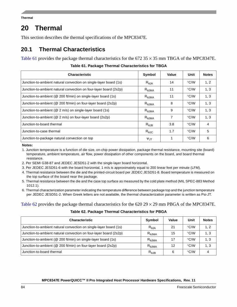
MPC8347E PowerQUICC™ II Pro Integrated Host Processor Hardware Specifications, Rev. 11
84 Freescale Semiconductor
Thermal
20 ThermalThis section describes the thermal specifications of the MPC8347E.
20.1 Thermal CharacteristicsTable 61 provides the package thermal characteristics for the 672 35 × 35 mm TBGA of the MPC8347E.
Table 62 provides the package thermal characteristics for the 620 29 × 29 mm PBGA of the MPC8347E.
Table 61. Package Thermal Characteristics for TBGA
Characteristic Symbol Value Unit Notes
Junction-to-ambient natural convection on single-layer board (1s) RθJA 14 °C/W 1, 2
Junction-to-ambient natural convection on four-layer board (2s2p) RθJMA 11 °C/W 1, 3
Junction-to-ambient (@ 200 ft/min) on single-layer board (1s) RθJMA 11 °C/W 1, 3
Junction-to-ambient (@ 200 ft/min) on four-layer board (2s2p) RθJMA 8 °C/W 1, 3
Junction-to-ambient (@ 2 m/s) on single-layer board (1s) RθJMA 9 °C/W 1, 3
Junction-to-ambient (@ 2 m/s) on four-layer board (2s2p) RθJMA 7 °C/W 1, 3
Junction-to-board thermal RθJB 3.8 °C/W 4
Junction-to-case thermal RθJC 1.7 °C/W 5
Junction-to-package natural convection on top ψJT 1 °C/W 6
Notes:1. Junction temperature is a function of die size, on-chip power dissipation, package thermal resistance, mounting site (board)
temperature, ambient temperature, air flow, power dissipation of other components on the board, and board thermal resistance.
2. Per SEMI G38-87 and JEDEC JESD51-2 with the single-layer board horizontal.3. Per JEDEC JESD51-6 with the board horizontal, 1 m/s is approximately equal to 200 linear feet per minute (LFM).4. Thermal resistance between the die and the printed-circuit board per JEDEC JESD51-8. Board temperature is measured on
the top surface of the board near the package.5. Thermal resistance between the die and the case top surface as measured by the cold plate method (MIL SPEC-883 Method
1012.1).6. Thermal characterization parameter indicating the temperature difference between package top and the junction temperature
per JEDEC JESD51-2. When Greek letters are not available, the thermal characterization parameter is written as Psi-JT.
Table 62. Package Thermal Characteristics for PBGA
Characteristic Symbol Value Unit Notes
Junction-to-ambient natural convection on single-layer board (1s) RθJA 21 °C/W 1, 2
Junction-to-ambient natural convection on four-layer board (2s2p) RθJMA 15 °C/W 1, 3
Junction-to-ambient (@ 200 ft/min) on single-layer board (1s) RθJMA 17 °C/W 1, 3
Junction-to-ambient (@ 200 ft/min) on four-layer board (2s2p) RθJMA 12 °C/W 1, 3
Junction-to-board thermal RθJB 6 °C/W 4

MPC8347E PowerQUICC™ II Pro Integrated Host Processor Hardware Specifications, Rev. 11
Freescale Semiconductor 85
Thermal
20.2 Thermal Management InformationFor the following sections, PD = (VDD × IDD) + PI/O where PI/O is the power dissipation of the I/O drivers. See Table 5 for I/O power dissipation values.
20.2.1 Estimation of Junction Temperature with Junction-to-Ambient Thermal Resistance
An estimation of the chip junction temperature, TJ, can be obtained from the equation:
TJ = TA + (RθJA × PD)
where:TJ = junction temperature (°C)
TA = ambient temperature for the package (°C)
RθJA = junction-to-ambient thermal resistance (°C/W)
PD = power dissipation in the package (W)
The junction-to-ambient thermal resistance is an industry-standard value that provides a quick and easy estimation of thermal performance. Generally, the value obtained on a single-layer board is appropriate for a tightly packed printed-circuit board. The value obtained on the board with the internal planes is usually appropriate if the board has low power dissipation and the components are well separated. Test cases have demonstrated that errors of a factor of two (in the quantity TJ – TA) are possible.
20.2.2 Estimation of Junction Temperature with Junction-to-Board Thermal Resistance
The thermal performance of a device cannot be adequately predicted from the junction-to-ambient thermal resistance. The thermal performance of any component is strongly dependent on the power dissipation of surrounding components. In addition, the ambient temperature varies widely within the application. For
Junction-to-case thermal RθJC 5 °C/W 5
Junction-to-package natural convection on top ψJT 5 °C/W 6
Notes1. Junction temperature is a function of die size, on-chip power dissipation, package thermal resistance, mounting site (board)
temperature, ambient temperature, air flow, power dissipation of other components on the board, and board thermal resistance.
2. Per SEMI G38-87 and JEDEC JESD51-2 with the single-layer board horizontal.3. Per JEDEC JESD51-6 with the board horizontal.4. Thermal resistance between the die and the printed-circuit board per JEDEC JESD51-8. Board temperature is measured on
the top surface of the board near the package.5. Thermal resistance between the die and the case top surface as measured by the cold plate method (MIL SPEC-883 Method
1012.1).6. Thermal characterization parameter indicating the temperature difference between package top and the junction temperature
per JEDEC JESD51-2. When Greek letters are not available, the thermal characterization parameter is written as Psi-JT.
Table 62. Package Thermal Characteristics for PBGA (continued)
Characteristic Symbol Value Unit Notes
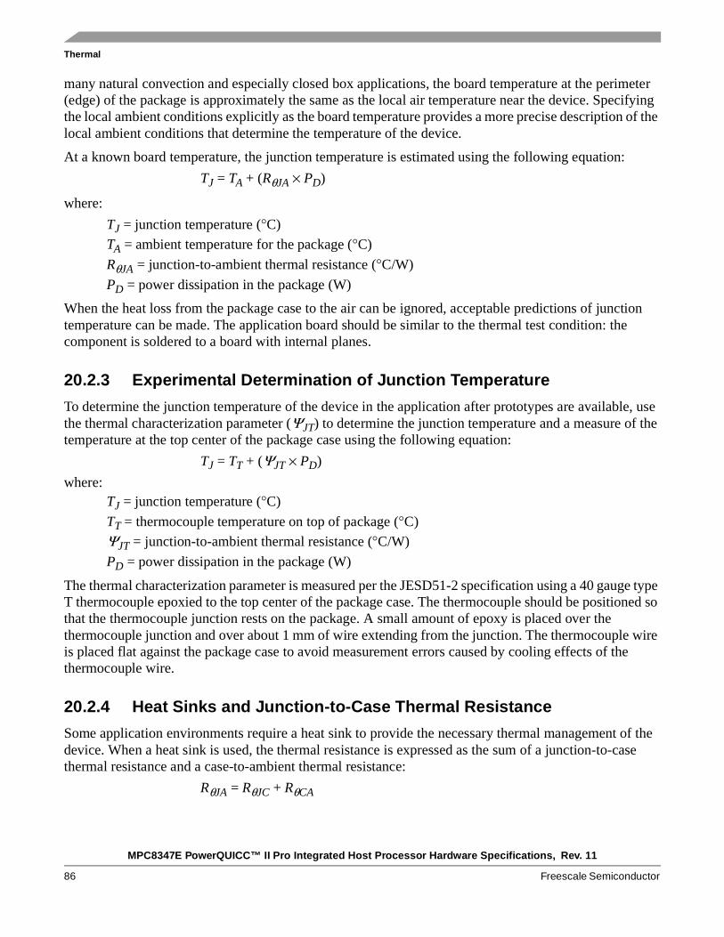
MPC8347E PowerQUICC™ II Pro Integrated Host Processor Hardware Specifications, Rev. 11
86 Freescale Semiconductor
Thermal
many natural convection and especially closed box applications, the board temperature at the perimeter (edge) of the package is approximately the same as the local air temperature near the device. Specifying the local ambient conditions explicitly as the board temperature provides a more precise description of the local ambient conditions that determine the temperature of the device.
At a known board temperature, the junction temperature is estimated using the following equation:
TJ = TA + (RθJA × PD)
where:
TJ = junction temperature (°C)
TA = ambient temperature for the package (°C)
RθJA = junction-to-ambient thermal resistance (°C/W)
PD = power dissipation in the package (W)
When the heat loss from the package case to the air can be ignored, acceptable predictions of junction temperature can be made. The application board should be similar to the thermal test condition: the component is soldered to a board with internal planes.
20.2.3 Experimental Determination of Junction Temperature
To determine the junction temperature of the device in the application after prototypes are available, use the thermal characterization parameter (ΨJT) to determine the junction temperature and a measure of the temperature at the top center of the package case using the following equation:
TJ = TT + (ΨJT × PD)
where:TJ = junction temperature (°C)
TT = thermocouple temperature on top of package (°C)
ΨJT = junction-to-ambient thermal resistance (°C/W)
PD = power dissipation in the package (W)
The thermal characterization parameter is measured per the JESD51-2 specification using a 40 gauge type T thermocouple epoxied to the top center of the package case. The thermocouple should be positioned so that the thermocouple junction rests on the package. A small amount of epoxy is placed over the thermocouple junction and over about 1 mm of wire extending from the junction. The thermocouple wire is placed flat against the package case to avoid measurement errors caused by cooling effects of the thermocouple wire.
20.2.4 Heat Sinks and Junction-to-Case Thermal Resistance
Some application environments require a heat sink to provide the necessary thermal management of the device. When a heat sink is used, the thermal resistance is expressed as the sum of a junction-to-case thermal resistance and a case-to-ambient thermal resistance:
RθJA = RθJC + RθCA
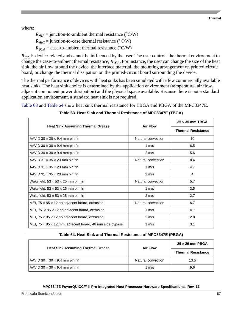
MPC8347E PowerQUICC™ II Pro Integrated Host Processor Hardware Specifications, Rev. 11
Freescale Semiconductor 87
Thermal
where:RθJA = junction-to-ambient thermal resistance (°C/W)
RθJC = junction-to-case thermal resistance (°C/W)
RθCA = case-to-ambient thermal resistance (°C/W)
RθJC is device-related and cannot be influenced by the user. The user controls the thermal environment to change the case-to-ambient thermal resistance, RθCA. For instance, the user can change the size of the heat sink, the air flow around the device, the interface material, the mounting arrangement on printed-circuit board, or change the thermal dissipation on the printed-circuit board surrounding the device.
The thermal performance of devices with heat sinks has been simulated with a few commercially available heat sinks. The heat sink choice is determined by the application environment (temperature, air flow, adjacent component power dissipation) and the physical space available. Because there is not a standard application environment, a standard heat sink is not required.
Table 63 and Table 64 show heat sink thermal resistance for TBGA and PBGA of the MPC8347E.
f
Table 63. Heat Sink and Thermal Resistance of MPC8347E (TBGA)
Heat Sink Assuming Thermal Grease Air Flow35 × 35 mm TBGA
Thermal Resistance
AAVID 30 × 30 × 9.4 mm pin fin Natural convection 10
AAVID 30 × 30 × 9.4 mm pin fin 1 m/s 6.5
AAVID 30 × 30 × 9.4 mm pin fin 2 m/s 5.6
AAVID 31 × 35 × 23 mm pin fin Natural convection 8.4
AAVID 31 × 35 × 23 mm pin fin 1 m/s 4.7
AAVID 31 × 35 × 23 mm pin fin 2 m/s 4
Wakefield, 53 × 53 × 25 mm pin fin Natural convection 5.7
Wakefield, 53 × 53 × 25 mm pin fin 1 m/s 3.5
Wakefield, 53 × 53 × 25 mm pin fin 2 m/s 2.7
MEI, 75 × 85 × 12 no adjacent board, extrusion Natural convection 6.7
MEI, 75 × 85 × 12 no adjacent board, extrusion 1 m/s 4.1
MEI, 75 × 85 × 12 no adjacent board, extrusion 2 m/s 2.8
MEI, 75 × 85 × 12 mm, adjacent board, 40 mm side bypass 1 m/s 3.1
Table 64. Heat Sink and Thermal Resistance of MPC8347E (PBGA)
Heat Sink Assuming Thermal Grease Air Flow29 × 29 mm PBGA
Thermal Resistance
AAVID 30 × 30 × 9.4 mm pin fin Natural convection 13.5
AAVID 30 × 30 × 9.4 mm pin fin 1 m/s 9.6
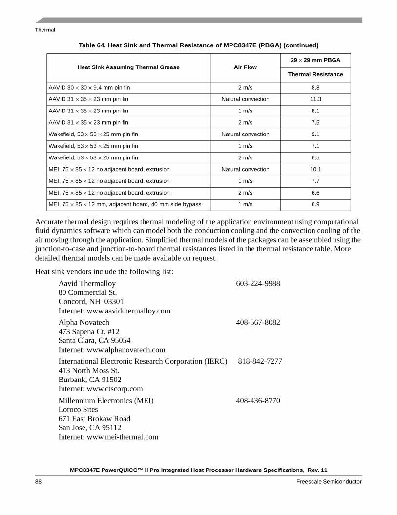
MPC8347E PowerQUICC™ II Pro Integrated Host Processor Hardware Specifications, Rev. 11
88 Freescale Semiconductor
Thermal
Accurate thermal design requires thermal modeling of the application environment using computational fluid dynamics software which can model both the conduction cooling and the convection cooling of the air moving through the application. Simplified thermal models of the packages can be assembled using the junction-to-case and junction-to-board thermal resistances listed in the thermal resistance table. More detailed thermal models can be made available on request.
Heat sink vendors include the following list:
Aavid Thermalloy 603-224-998880 Commercial St.Concord, NH 03301Internet: www.aavidthermalloy.com
Alpha Novatech 408-567-8082473 Sapena Ct. #12Santa Clara, CA 95054Internet: www.alphanovatech.com
International Electronic Research Corporation (IERC) 818-842-7277413 North Moss St.Burbank, CA 91502Internet: www.ctscorp.com
Millennium Electronics (MEI) 408-436-8770Loroco Sites671 East Brokaw RoadSan Jose, CA 95112Internet: www.mei-thermal.com
AAVID 30 × 30 × 9.4 mm pin fin 2 m/s 8.8
AAVID 31 × 35 × 23 mm pin fin Natural convection 11.3
AAVID 31 × 35 × 23 mm pin fin 1 m/s 8.1
AAVID 31 × 35 × 23 mm pin fin 2 m/s 7.5
Wakefield, 53 × 53 × 25 mm pin fin Natural convection 9.1
Wakefield, 53 × 53 × 25 mm pin fin 1 m/s 7.1
Wakefield, 53 × 53 × 25 mm pin fin 2 m/s 6.5
MEI, 75 × 85 × 12 no adjacent board, extrusion Natural convection 10.1
MEI, 75 × 85 × 12 no adjacent board, extrusion 1 m/s 7.7
MEI, 75 × 85 × 12 no adjacent board, extrusion 2 m/s 6.6
MEI, 75 × 85 × 12 mm, adjacent board, 40 mm side bypass 1 m/s 6.9
Table 64. Heat Sink and Thermal Resistance of MPC8347E (PBGA) (continued)
Heat Sink Assuming Thermal Grease Air Flow29 × 29 mm PBGA
Thermal Resistance
MPC8347E PowerQUICC™ II Pro Integrated Host Processor Hardware Specifications, Rev. 11
Freescale Semiconductor 89
Thermal
Tyco Electronics 800-522-2800Chip Coolers™P.O. Box 3668Harrisburg, PA 17105-3668Internet: www.chipcoolers.com
Wakefield Engineering 603-635-510233 Bridge St.Pelham, NH 03076Internet: www.wakefield.com
Interface material vendors include the following:
Chomerics, Inc. 781-935-485077 Dragon Ct.Woburn, MA 01801Internet: www.chomerics.com
Dow-Corning Corporation 800-248-2481Dow-Corning Electronic MaterialsP.O. Box 994Midland, MI 48686-0997Internet: www.dowcorning.com
Shin-Etsu MicroSi, Inc. 888-642-767410028 S. 51st St.Phoenix, AZ 85044Internet: www.microsi.com
The Bergquist Company 800-347-457218930 West 78th St.Chanhassen, MN 55317Internet: www.bergquistcompany.com
20.3 Heat Sink AttachmentWhen heat sinks are attached, an interface material is required, preferably thermal grease and a spring clip. The spring clip should connect to the printed-circuit board, either to the board itself, to hooks soldered to the board, or to a plastic stiffener. Avoid attachment forces that can lift the edge of the package or peel the package from the board. Such peeling forces reduce the solder joint lifetime of the package. The recommended maximum force on the top of the package is 10 lb force (4.5 kg force). Any adhesive attachment should attach to painted or plastic surfaces, and its performance should be verified under the application requirements.
20.3.1 Experimental Determination of the Junction Temperature with a Heat Sink
When a heat sink is used, the junction temperature is determined from a thermocouple inserted at the interface between the case of the package and the interface material. A clearance slot or hole is normally
MPC8347E PowerQUICC™ II Pro Integrated Host Processor Hardware Specifications, Rev. 11
90 Freescale Semiconductor
Thermal
required in the heat sink. Minimize the size of the clearance to minimize the change in thermal performance caused by removing part of the thermal interface to the heat sink. Because of the experimental difficulties with this technique, many engineers measure the heat sink temperature and then back calculate the case temperature using a separate measurement of the thermal resistance of the interface. From this case temperature, the junction temperature is determined from the junction-to-case thermal resistance.
TJ = TC + (RθJC × PD)
where:TJ = junction temperature (°C)
TC = case temperature of the package (°C)
RθJC = junction-to-case thermal resistance (°C/W)
PD = power dissipation (W)
MPC8347E PowerQUICC™ II Pro Integrated Host Processor Hardware Specifications, Rev. 11
Freescale Semiconductor 91
System Design Information
21 System Design InformationThis section provides electrical and thermal design recommendations for successful application of the MPC8347E.
21.1 System ClockingThe MPC8347E includes two PLLs:
1. The platform PLL generates the platform clock from the externally supplied CLKIN input. The frequency ratio between the platform and CLKIN is selected using the platform PLL ratio configuration bits as described in Section 19.1, “System PLL Configuration.”
2. The e300 core PLL generates the core clock as a slave to the platform clock. The frequency ratio between the e300 core clock and the platform clock is selected using the e300 PLL ratio configuration bits as described in Section 19.2, “Core PLL Configuration.”
21.2 PLL Power Supply FilteringEach PLL gets power through independent power supply pins (AVDD1, AVDD2, respectively). The AVDD level should always equal to VDD, and preferably these voltages are derived directly from VDD through a low frequency filter scheme.
There are a number of ways to provide power reliably to the PLLs, but the recommended solution is to provide four independent filter circuits as illustrated in Figure 42, one to each of the four AVDD pins. Independent filters to each PLL reduce the opportunity to cause noise injection from one PLL to the other.
The circuit filters noise in the PLL resonant frequency range from 500 kHz to 10 MHz. It should be built with surface mount capacitors with minimum effective series inductance (ESL). Consistent with the recommendations of Dr. Howard Johnson in High Speed Digital Design: A Handbook of Black Magic (Prentice Hall, 1993), multiple small capacitors of equal value are recommended over a single large value capacitor.
To minimize noise coupled from nearby circuits, each circuit should be placed as closely as possible to the specific AVDD pin being supplied. It should be possible to route directly from the capacitors to the AVDD pin, which is on the periphery of package, without the inductance of vias.
Figure 42 shows the PLL power supply filter circuit.
Figure 42. PLL Power Supply Filter Circuit
VDD AVDD (or L2AVDD)
2.2 µF 2.2 µF
GNDLow ESL Surface Mount Capacitors
10 Ω
MPC8347E PowerQUICC™ II Pro Integrated Host Processor Hardware Specifications, Rev. 11
92 Freescale Semiconductor
System Design Information
21.3 Decoupling RecommendationsDue to large address and data buses and high operating frequencies, the MPC8347E can generate transient power surges and high frequency noise in its power supply, especially while driving large capacitive loads. This noise must be prevented from reaching other components in the MPC8347E system, and the MPC8347E itself requires a clean, tightly regulated source of power. Therefore, the system designer should place at least one decoupling capacitor at each VDD, OVDD, GVDD, and LVDD pin of the MPC8347E. These capacitors should receive their power from separate VDD, OVDD, GVDD, LVDD, and GND power planes in the PCB, with short traces to minimize inductance. Capacitors can be placed directly under the device using a standard escape pattern. Others can surround the part.
These capacitors should have a value of 0.01 or 0.1 µF. Only ceramic SMT (surface mount technology) capacitors should be used to minimize lead inductance, preferably 0402 or 0603 sizes.
In addition, distribute several bulk storage capacitors around the PCB, feeding the VDD, OVDD, GVDD, and LVDD planes, to enable quick recharging of the smaller chip capacitors. These bulk capacitors should have a low ESR (equivalent series resistance) rating to ensure the quick response time. They should also be connected to the power and ground planes through two vias to minimize inductance. Suggested bulk capacitors are 100–330 µF (AVX TPS tantalum or Sanyo OSCON).
21.4 Connection RecommendationsTo ensure reliable operation, connect unused inputs to an appropriate signal level. Unused active low inputs should be tied to OVDD, GVDD, or LVDD as required. Unused active high inputs should be connected to GND. All NC (no-connect) signals must remain unconnected.
Power and ground connections must be made to all external VDD, GVDD, LVDD, OVDD, and GND pins of the MPC8347E.
21.5 Output Buffer DC ImpedanceThe MPC8347E drivers are characterized over process, voltage, and temperature. For all buses, the driver is a push-pull single-ended driver type (open drain for I2C).
To measure Z0 for the single-ended drivers, an external resistor is connected from the chip pad to OVDD or GND. Then the value of each resistor is varied until the pad voltage is OVDD/2 (see Figure 43). The output impedance is the average of two components, the resistances of the pull-up and pull-down devices. When data is held high, SW1 is closed (SW2 is open) and RP is trimmed until the voltage at the pad equals OVDD/2. RP then becomes the resistance of the pull-up devices. RP and RN are designed to be close to each other in value. Then, Z0 = (RP + RN)/2.

MPC8347E PowerQUICC™ II Pro Integrated Host Processor Hardware Specifications, Rev. 11
Freescale Semiconductor 93
System Design Information
Figure 43. Driver Impedance Measurement
Two measurements give the value of this resistance and the strength of the driver current source. First, the output voltage is measured while driving logic 1 without an external differential termination resistor. The measured voltage is V1 = Rsource × Isource. Second, the output voltage is measured while driving logic 1 with an external precision differential termination resistor of value Rterm. The measured voltage is V2 = (1/(1/R1 + 1/R2)) × Isource. Solving for the output impedance gives Rsource = Rterm × (V1/V2 – 1). The drive current is then Isource = V1/Rsource.
Table 65 summarizes the signal impedance targets. The driver impedance are targeted at minimum VDD, nominal OVDD, 105°C.
21.6 Configuration Pin MultiplexingThe MPC8347E power-on configuration options can be set through external pull-up or pull-down resistors of 4.7 kΩ on certain output pins (see the customer-visible configuration pins). These pins are used as output only pins in normal operation.
However, while HRESET is asserted, these pins are treated as inputs, and the value on these pins is latched when PORESET deasserts. Then the input receiver is disabled and the I/O circuit takes on its normal function. Careful board layout with stubless connections to these pull-up/pull-down resistors coupled with
Table 65. Impedance Characteristics
Impedance
Local Bus, Ethernet, DUART, Control,
Configuration, Power Management
PCI Signals(Not Including PCI
Output Clocks)
PCI Output Clocks(Including
PCI_SYNC_OUT) DDR DRAM Symbol Unit
RN 42 Target 25 Target 42 Target 20 Target Z0 Ω
RP 42 Target 25 Target 42 Target 20 Target Z0 Ω
Differential NA NA NA NA ZDIFF Ω
Note: Nominal supply voltages. See Table 1, Tj = 105°C.
OVDD
OGND
RP
RN
PadData
SW1
SW2
MPC8347E PowerQUICC™ II Pro Integrated Host Processor Hardware Specifications, Rev. 11
94 Freescale Semiconductor
System Design Information
the large value of the pull-up/pull-down resistor should minimize the disruption of signal quality or speed for the output pins.
21.7 Pull-Up Resistor RequirementsThe MPC8347E requires high resistance pull-up resistors (10 kΩ is recommended) on open-drain pins, including I2C pins, the Ethernet Management MDIO pin, and IPIC interrupt pins.
For more information on required pull-up resistors and the connections required for the JTAG interface, refer to application note AN2931, PowerQUICC™ Design Checklist.
MPC8347E PowerQUICC™ II Pro Integrated Host Processor Hardware Specifications, Rev. 11
Freescale Semiconductor 95
Document Revision History
22 Document Revision HistoryTable 66 provides a revision history of this document.
Table 66. Document Revision History
Revision Date Substantive Change(s)
11 2/2009 In Section 21.1, “System Clocking,” removed “(AVDD1)” and “(AVDD2”) from bulleted list.
In Section 21.2, “PLL Power Supply Filtering,” in the second paragraph, changed “provide five independent filter circuits,” and “the five AVDD pins” to provide four independent filter circuits,” and “the four AVDD pins.”
In Table 35, removed row for rise time (tI2CR). Removed minimum value of tI2CF. Added note 5 stating that the device does not follow the I2C-BUS Specifications version 2.1 regarding the tI2CF AC
parameter.
In Table 54, corrected the max csb_clk to 266 MHz.
In Table 60, added PLL configurations 903, 923, A03, A23, and 503 for 533 MHz
In Table 35, corrected tLBKHOV parametr to tLBKLOV (output data is driven on falling edge of clock in DLL bypass mode). Similarly, made the same correction to Figure 21, Figure 23, and Figure 24 for output signals.
Added Figure 1 and Figure 4.
In Table 9.2, clarified that AC table is for ULPI only.
Added footnote 4 to Table 67.
In Table 67, updated note 1 to say the following: “For temperature range = C, processor frequency is up to 667(TBGA) with a platform frequency of 333 and limited to 400 (PBGA) with a platform frequency of 266.”
Added footnote 10 and 11 to Table 51 and Table 52.
In Table 51, Table 52, updated note 11 to say the following: “SEC1_TXD[3] is required an external pull-up resistor. For proper functionality of the device, this pin must be pulled up or actively driven high during a hard reset. No external pull-down resistors are allowed to be attached to this net.”
Added footnote 6 to Table 7.
In Table 7, updated the note 6 to say the following: “The Spread spectrum clocking. Is allowed with 1% input frequency down-spread at maximum 50KHz modulation rate regardless of input frequency.”
In 8.1.1, removed the note “The potential applied to the input of a GMII, MII, TBI, RGMII, or RTBI receiver may exceed the potential of the receiver power supply (that is, a RGMII driver powered from a 3.6 V supply driving VOH into a RGMII receiver powered from a 2.5-V supply). Tolerance for dissimilar RGMII driver and receiver supply potentials is implicit in these specifications.”
10 4/2007 In Table 3, “Output Drive Capability,” changed the values in the Output Impedance column and added USB to the seventh row.
In Table 54, “Operating Frequencies for TBGA,” added column for 400 MHz.
In Section 21.7, “Pull-Up Resistor Requirements,” deleted last two paragraphs and after first paragraph, added a new paragraph.
Deleted Section 21.8, “JTAG Configuration Signals,” and Figure 43, “JTAG Interface Connection.”
9 3/2007 In Table 54, “Operating Frequencies for TBGA,” in the ‘Coherent system bus frequency (csb_clk)’ row, changed the value in the 533 MHz column to 100–333.
In Table 60, “Suggested PLL Configurations,” under the subhead, ‘33 MHz CLKIN/PCI_CLK Options,’ added row A03 between Ref. No. 724 and 804. Under the subhead ‘66 MHz CLKIN/PCI_CLK Options,’ added row 503 between Ref. No. 305 and 404. For Ref. No. 306, changed the CORE PLL value to 0000110.
In Section 23, “Ordering Information,” replaced first paragraph and added a note.
In Section 23.1, “Part Numbers Fully Addressed by This Document,” replaced first paragraph.
MPC8347E PowerQUICC™ II Pro Integrated Host Processor Hardware Specifications, Rev. 11
96 Freescale Semiconductor
Document Revision History
8 2/2007 Page 1, updated first paragraph to reflect PowerQUICC II information. Updated note after second paragraph.
In the features list in Section 1, “Overview,” corrected DDR data rate to show:
• 266 MHz for PBGA parts for all silicon revisions • 333 MHz for DDR for TBGA parts for silicon Rev. 1.x In Table 5, “MPC8347E Typical I/O Power Dissipation,” added GVDD 1.8-V values for DDR2; added table footnote to designate rates that apply only to the TBGA package.
In Figure 43, “JTAG Interface Connection,” updated with new figure.
In Section 23, “Ordering Information,” replicated note from document introduction.
In Section 23.1, “Part Numbers Fully Addressed by This Document,” replaced third sentence of first paragraph directing customer to product summary page for available frequency configuration parts.
Updated back page information.
7 8/2006 Changed all references to revision 2.0 silicon to revision 3.0 silicon.
Changed VIH minimum value in Table 36, “JTAG Interface DC Electrical Characteristics,” to OVDD – 0.3.
In Table 60, “Suggested PLL Configurations,” deleted reference-number rows 902 and 703.
6 3/2006 Section 2, “Electrical Characteristics,” moved to second section and all other section, table, and figure numbering change accordingly.Table 7, “CLKIN AC Timing Specifications:” Changed max rise and fall time from 1.2 to 2.3.
Table 22, “GMII Receive AC Timing Specifications:” Changed min tTTKHDX from 0.5 to 1.0.
Table 30, “MII Management AC Timing Specifications:” Changed max value of tMDKHDX from 70 to 170.
Table 34, “Local Bus General Timing Parameters—DLL on:” Changed min tLBIVKH2 from 1.7 to 2.2.
Table 36, “JTAG interface DC Electrical Characteristics:” Changed VIH input high voltage min to 2.0.
Table 54, “Operating Frequencies for TBGA:”
• Updated TBD values. • Changed maximum coherent system bus frequency for TBGA 667-MHz device to 333 MHz.Table 55, “Operating Frequencies for PBGA:”
• Updated TBD values. • Changed PBGA maximum coherent system bus frequency to 266 MHz, and maximum DDR
memory bus frequency to 133 MHz.Table 60, “Suggested PLL Configurations”: Removed some values from suggested PLL configurations for reference numbers 902, 922, 903, and 923.
Table 67, “Part Numbering Nomenclature”: Updated TBD values in note 1.
Added Table 68, “SVR Settings.”Added Section 23.2, “Part Marking.”
5 10/2005 In Table 57, updated AAVID 30x30x9.4 mm Pin Fin (natural convection) junction-to-ambient thermal resistance, from 11 to 10.
4 9/2005 Added Table 2, “MPC8347E Typical I/O Power Dissipation.”
3 8/2005 Table 1: Updated values for power dissipation that were TBD in Revision 2.
2 5/2005 Table 1: Typical values for power dissipation are changed to TBD.Table 48: Footnote numbering was wrong. THERM0 should have footnote 9 instead of 8.
Table 66. Document Revision History (continued)
Revision Date Substantive Change(s)
MPC8347E PowerQUICC™ II Pro Integrated Host Processor Hardware Specifications, Rev. 11
Freescale Semiconductor 97
Document Revision History
1 4/2005 Table 1: Addition of note 1Table 48: Addition of Therm0 (K32)Table 49: Addition of Therm0 (B15)
0 4/2005 Initial release.
Table 66. Document Revision History (continued)
Revision Date Substantive Change(s)
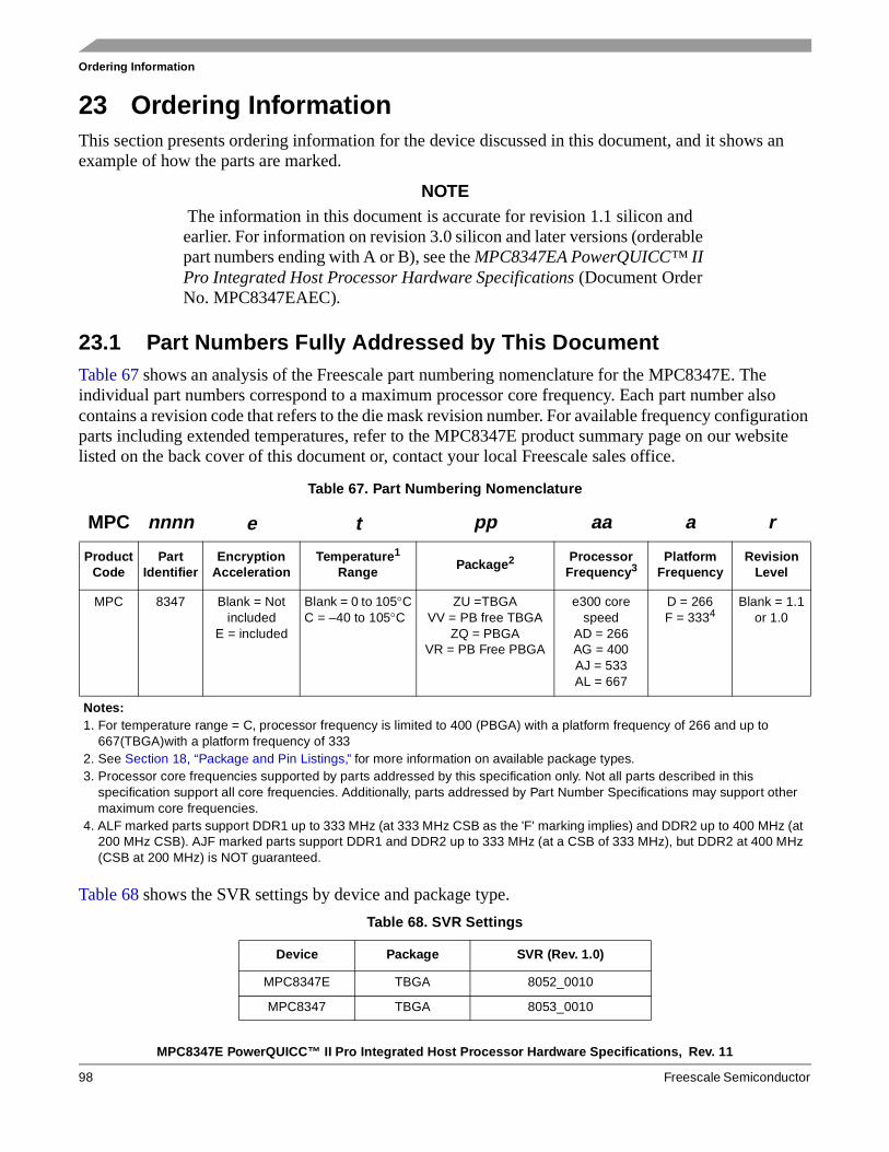
MPC8347E PowerQUICC™ II Pro Integrated Host Processor Hardware Specifications, Rev. 11
98 Freescale Semiconductor
Ordering Information
23 Ordering InformationThis section presents ordering information for the device discussed in this document, and it shows an example of how the parts are marked.
NOTE The information in this document is accurate for revision 1.1 silicon and earlier. For information on revision 3.0 silicon and later versions (orderable part numbers ending with A or B), see the MPC8347EA PowerQUICC™ II Pro Integrated Host Processor Hardware Specifications (Document Order No. MPC8347EAEC).
23.1 Part Numbers Fully Addressed by This DocumentTable 67 shows an analysis of the Freescale part numbering nomenclature for the MPC8347E. The individual part numbers correspond to a maximum processor core frequency. Each part number also contains a revision code that refers to the die mask revision number. For available frequency configuration parts including extended temperatures, refer to the MPC8347E product summary page on our website listed on the back cover of this document or, contact your local Freescale sales office.
Table 68 shows the SVR settings by device and package type.
Table 67. Part Numbering Nomenclature
MPC nnnn e t pp aa a r
ProductCode
PartIdentifier
EncryptionAcceleration
Temperature1 Range Package2 Processor
Frequency3Platform
FrequencyRevision
Level
MPC 8347 Blank = Not included
E = included
Blank = 0 to 105°CC = –40 to 105°C
ZU =TBGAVV = PB free TBGA
ZQ = PBGAVR = PB Free PBGA
e300 core speed
AD = 266AG = 400AJ = 533AL = 667
D = 266F = 3334
Blank = 1.1 or 1.0
Notes: 1. For temperature range = C, processor frequency is limited to 400 (PBGA) with a platform frequency of 266 and up to
667(TBGA)with a platform frequency of 3332. See Section 18, “Package and Pin Listings,” for more information on available package types.3. Processor core frequencies supported by parts addressed by this specification only. Not all parts described in this
specification support all core frequencies. Additionally, parts addressed by Part Number Specifications may support other maximum core frequencies.
4. ALF marked parts support DDR1 up to 333 MHz (at 333 MHz CSB as the 'F' marking implies) and DDR2 up to 400 MHz (at 200 MHz CSB). AJF marked parts support DDR1 and DDR2 up to 333 MHz (at a CSB of 333 MHz), but DDR2 at 400 MHz (CSB at 200 MHz) is NOT guaranteed.
Table 68. SVR Settings
Device Package SVR (Rev. 1.0)
MPC8347E TBGA 8052_0010
MPC8347 TBGA 8053_0010
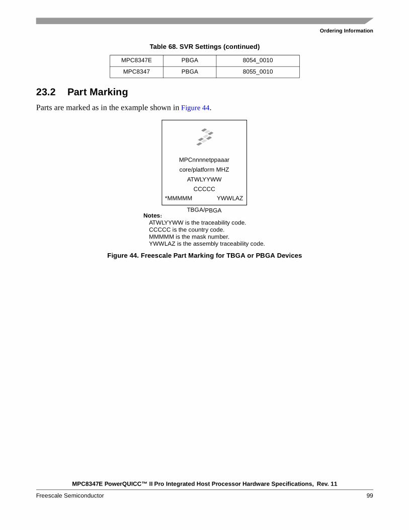
MPC8347E PowerQUICC™ II Pro Integrated Host Processor Hardware Specifications, Rev. 11
Freescale Semiconductor 99
Ordering Information
23.2 Part MarkingParts are marked as in the example shown in Figure 44.
Figure 44. Freescale Part Marking for TBGA or PBGA Devices
MPC8347E PBGA 8054_0010
MPC8347 PBGA 8055_0010
Table 68. SVR Settings (continued)
Notes:ATWLYYWW is the traceability code.
MPCnnnnetppaaar
core/platform MHZ
ATWLYYWW
CCCCC
TBGA/PBGA
*MMMMM YWWLAZ
CCCCC is the country code.MMMMM is the mask number.YWWLAZ is the assembly traceability code.
MPC8347E PowerQUICC™ II Pro Integrated Host Processor Hardware Specifications, Rev. 11
100 Freescale Semiconductor
Ordering Information
THIS PAGE INTENTIONALLY LEFT BLANK
MPC8347E PowerQUICC™ II Pro Integrated Host Processor Hardware Specifications, Rev. 11
Freescale Semiconductor 101
Ordering Information
THIS PAGE INTENTIONALLY LEFT BLANK
Information in this document is provided solely to enable system and software
implementers to use Freescale Semiconductor products. There are no express or
implied copyright licenses granted hereunder to design or fabricate any integrated
circuits or integrated circuits based on the information in this document.
Freescale Semiconductor reserves the right to make changes without further notice to
any products herein. Freescale Semiconductor makes no warranty, representation or
guarantee regarding the suitability of its products for any particular purpose, nor does
Freescale Semiconductor assume any liability arising out of the application or use of
any product or circuit, and specifically disclaims any and all liability, including without
limitation consequential or incidental damages. “Typical” parameters which may be
provided in Freescale Semiconductor data sheets and/or specifications can and do
vary in different applications and actual performance may vary over time. All operating
parameters, including “Typicals” must be validated for each customer application by
customer’s technical experts. Freescale Semiconductor does not convey any license
under its patent rights nor the rights of others. Freescale Semiconductor products are
not designed, intended, or authorized for use as components in systems intended for
surgical implant into the body, or other applications intended to support or sustain life,
or for any other application in which the failure of the Freescale Semiconductor product
could create a situation where personal injury or death may occur. Should Buyer
purchase or use Freescale Semiconductor products for any such unintended or
unauthorized application, Buyer shall indemnify and hold Freescale Semiconductor
and its officers, employees, subsidiaries, affiliates, and distributors harmless against all
claims, costs, damages, and expenses, and reasonable attorney fees arising out of,
directly or indirectly, any claim of personal injury or death associated with such
unintended or unauthorized use, even if such claim alleges that Freescale
Semiconductor was negligent regarding the design or manufacture of the part.
How to Reach Us:
Home Page: www.freescale.com
Web Support: http://www.freescale.com/support
USA/Europe or Locations Not Listed: Freescale Semiconductor, Inc.Technical Information Center, EL5162100 East Elliot Road Tempe, Arizona 85284 +1-800-521-6274 or+1-480-768-2130www.freescale.com/support
Europe, Middle East, and Africa:Freescale Halbleiter Deutschland GmbHTechnical Information CenterSchatzbogen 781829 Muenchen, Germany+44 1296 380 456 (English) +46 8 52200080 (English)+49 89 92103 559 (German)+33 1 69 35 48 48 (French) www.freescale.com/support
Japan: Freescale Semiconductor Japan Ltd. HeadquartersARCO Tower 15F1-8-1, Shimo-Meguro, Meguro-ku Tokyo 153-0064Japan 0120 191014 or+81 3 5437 [email protected]
Asia/Pacific: Freescale Semiconductor Hong Kong Ltd. Technical Information Center2 Dai King Street Tai Po Industrial Estate Tai Po, N.T., Hong Kong +800 2666 [email protected]
For Literature Requests Only:Freescale Semiconductor
Literature Distribution Center P.O. Box 5405Denver, Colorado 80217 +1-800 441-2447 or+1-303-675-2140Fax: +1-303-675-2150LDCForFreescaleSemiconductor
@hibbertgroup.com
Freescale™ and the Freescale logo are trademarks of Freescale Semiconductor, Inc. The Power Architecture and Power.org word marks and the Power and Power.org logos and related marks are trademarks and service marks licensed by Power.org. IIEEE 802.3, 802.3u, 802.3x, 802.3z, 802.3ac, 802.11i, and 1149.1 are trademarks or registered trademarks of the Institute of Electrical and Electronics Engineers, Inc. (IEEE). This product is not endorsed or approved by the IEEE. All other product or service names are the property of their respective owners.
© Freescale Semiconductor, Inc., 2005–2009. All rights reserved.
Document Number: MPC8347EECRev. 1102/2009