modern design principles risc and cisc - edward bosworth · • risc is not a set of rules; there...
TRANSCRIPT

Modern Design Principles RISC and CISC,
Multicore
Edward L. Bosworth, Ph.D.
Computer Science Department
Columbus State University
The von Neumann Inheritance
• The EDVAC, designed in 1945, was one of the first stored program machines.
• All modern computers are modifications of this design; only the technical implementation has been changed.
• Other designs have been suggested, emulated on a von Neumann machine, and abandoned because the emulation worked so well.
2

General-purpose and Special-purpose
• Most computers are general-purpose devices, tailored to a given purpose by the software.
• Sometimes a high-volume market demand justifies a special-purpose design. Examples:
• 1. Routers used on the Internet.
• 2. Graphics cards, such as the NVIDIA cards.
• NVIDIA has launched the CUDA (Compute Unified Device Architecture), allowing the graphics card to be used as a standard CPU.
3

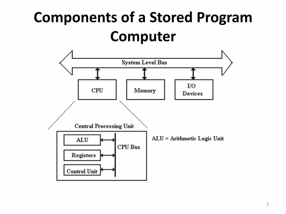
Components of a Stored Program Computer
• The four major components of a modern stored program computer are:
1. The Central Processing Unit (CPU)
2. The Primary Memory (also called “core memory” or “main memory”)
3. The Input / Output system
4. One or more system busses to allow the components to communicate.
4
Components of a Stored Program Computer
5

The Simple Top Level Model
Logically speaking, the computer has one bus used to allow all components to communicate.
Early designs, such as the PDP-11, had only one bus. For these slow machines, it worked well.
6

Realistic Organizations
• The design on the previous slide is logically correct, but IT WON’T WORK.
• IT IS TOO SLOW. Problem: A single system level bus cannot handle the load.
• Modern gamers demand fast video; this requires a fast bus to the video chip.
• The memory system is always a performance bottleneck. We need a dedicated memory bus in order to allow acceptable performance.
7

Revision of the Design
• Legacy I/O devices of various speeds must be accommodated by the design.
• Here an I/O Control Hub (ICH) manages two busses, one for legacy devices.
8

Current State of the Design
9
The Chip Set
• The term “chip set” refers to a set of VLSI chips that are designed to work together.
• The chip set is specific to a given CPU. It mostly relates to chips on the mother board.
• Based on Intel Pentium-class microprocessors, the term chipset often refers to a specific pair of chips on the motherboard: the Northbridge and the Southbridge.
10

North and South
• The Northbridge links the CPU to very high-speed devices, especially main memory and graphics controllers, and the Southbridge connects to lower-speed peripheral buses (such as PCI or ISA). In many modern chipsets, the Southbridge contains some on-chip integrated peripherals, such as Ethernet, USB, and audio devices.
11

Multi-Level Memory
• What we want is a very large memory, in which each memory element is fabricated from very fast components. But fast means expensive.
• What we can afford is a very large memory, in which each memory element is fabricated from moderately fast, but inexpensive, components.
• Modern computers achieve good performance from a large, moderately fast, main memory by using a multi-level cache memory.
• Quite often, there are 2 or 3 levels of cache.
12

A Modern Two-Level Cache
• All Pentium designs have at least two levels of cache memory. L2 holds 1 to 2 MB.
• The L1 cache is split, with an Instruction Cache and a Data Cache.
13

The Split L1 Cache
• Memory can do only one thing at a time.
• The split L1 cache is realized as 2 independent very fast memories. The CPU can access both at the same time.
• This parallel access allows modern CPU design tricks, especially pipelining.
• The CPU does not write back to the L1 I cache That makes the I cache simpler and faster.
14

Cache and the Pipeline
• Instruction Fetch reads the I cache.
RISC
• The acronym RISC stands for “Reduced Instruction Set Computer”. • RISC represents a design philosophy for the ISA (Instruction Set
Architecture) and the CPU microarchitecture that implements that ISA. • RISC is not a set of rules; there is no “pure RISC” design. • The acronym CISC, standing for “Complex Instruction Set Computer”, is a
term applied to computers that do not follow that design. • The first designed called “RISC” date to the early 1980’s. The movement
began with two experimental designs • The IBM 801 developed by IBM in 1980 • The RISC I developed by UC Berkeley in 1981. • We should note that the original RISC machine was probably the CDC–
6400 designed by Mr. Seymour Cray, of the Control Data Corporation. • In designing a CPU that was simple and very fast, Mr. Cray applied many of
the techniques that would later be called “RISC” without himself using the term.

Why CISC?
• Early CPU designs could have followed the RISC philosophy, the advantages of which were apparent early. Why then was the CISC design followed?
• Here are two reasons: • 1. CISC designs make more efficient use of memory. In particular,
the “code density” is better, more instructions per kilobyte. • After all, memory was very expensive and prone to failure. • • 2. CISC designs close the “semantic gap”; they produce an ISA
with instructions that more closely resemble those in a higher–level language. This should provide better support for the compilers.
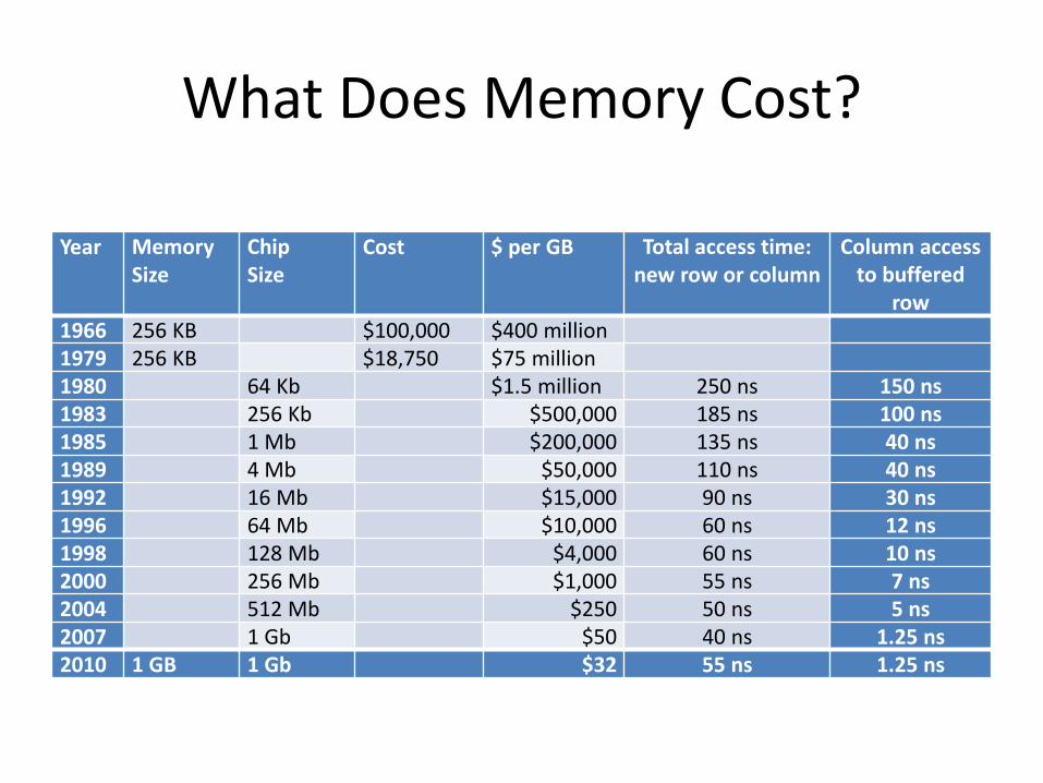
What Does Memory Cost?
Year Memory Size
Chip Size
Cost $ per GB Total access time: new row or column
Column access to buffered
row
1966 256 KB $100,000 $400 million 1979 256 KB $18,750 $75 million 1980 64 Kb $1.5 million 250 ns 150 ns
1983 256 Kb $500,000 185 ns 100 ns
1985 1 Mb $200,000 135 ns 40 ns
1989 4 Mb $50,000 110 ns 40 ns
1992 16 Mb $15,000 90 ns 30 ns
1996 64 Mb $10,000 60 ns 12 ns
1998 128 Mb $4,000 60 ns 10 ns
2000 256 Mb $1,000 55 ns 7 ns
2004 512 Mb $250 50 ns 5 ns
2007 1 Gb $50 40 ns 1.25 ns
2010 1 GB 1 Gb $32 55 ns 1.25 ns
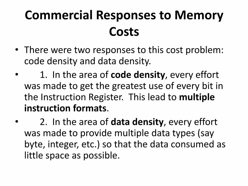
Commercial Responses to Memory Costs
• There were two responses to this cost problem: code density and data density.
• 1. In the area of code density, every effort was made to get the greatest use of every bit in the Instruction Register. This lead to multiple instruction formats.
• 2. In the area of data density, every effort was made to provide multiple data types (say byte, integer, etc.) so that the data consumed as little space as possible.
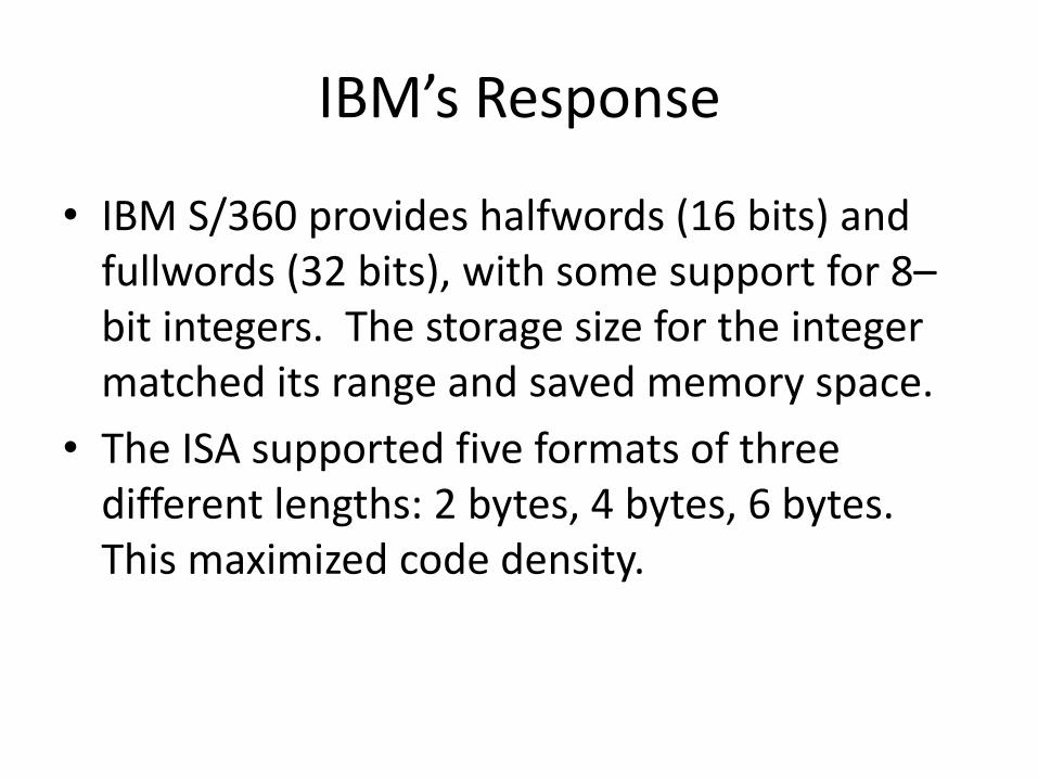
IBM’s Response
• IBM S/360 provides halfwords (16 bits) and fullwords (32 bits), with some support for 8–bit integers. The storage size for the integer matched its range and saved memory space.
• The ISA supported five formats of three different lengths: 2 bytes, 4 bytes, 6 bytes. This maximized code density.
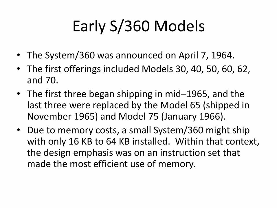
Early S/360 Models
• The System/360 was announced on April 7, 1964.
• The first offerings included Models 30, 40, 50, 60, 62, and 70.
• The first three began shipping in mid–1965, and the last three were replaced by the Model 65 (shipped in November 1965) and Model 75 (January 1966).
• Due to memory costs, a small System/360 might ship with only 16 KB to 64 KB installed. Within that context, the design emphasis was on an instruction set that made the most efficient use of memory.

IBM S/360 Registers
• While memory was expensive, registers made from transistors were more expensive.
• Each computer in the S/360 family had 16 general purpose 32–bit registers. These were logical constructs.
• The organization of the different models called for registers to be realized in rather different ways.
• Model 30 Dedicated storage locations in main memory • Models 40 and 50
A dedicated core array, distinct from main memory. • Models 60, 62, and 70
True data flip–flops, implemented as transistors.
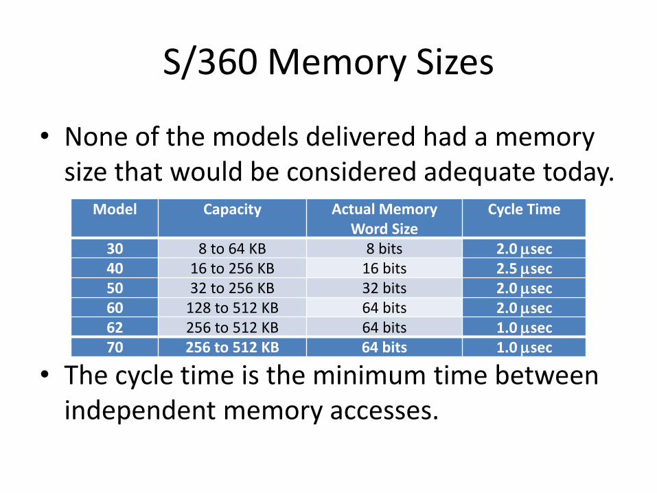
S/360 Memory Sizes
• None of the models delivered had a memory size that would be considered adequate today.
• The cycle time is the minimum time between independent memory accesses.
Model Capacity Actual Memory Word Size
Cycle Time
30 8 to 64 KB 8 bits 2.0 sec
40 16 to 256 KB 16 bits 2.5 sec
50 32 to 256 KB 32 bits 2.0 sec
60 128 to 512 KB 64 bits 2.0 sec
62 256 to 512 KB 64 bits 1.0 sec
70 256 to 512 KB 64 bits 1.0 sec
Support for High Level Languages
• Another justification for the Complex ISA was that the complexity would facilitate the development of compilers for high level languages, such as FORTRAN and COBOL.
• Hypothesis: If the hardware directly supported complex structures, the compiler writer would have an easier task.
• This hypothesis was late in being tested.

Realities of HLL Support
• Experimental studies conducted in 1971 by Donald Knuth and in 1982 by David Patterson showed that
• 1) nearly 85% of a programs statements were simple assignment, conditional, or procedure calls.
• 2) None of these required a complicated instruction set.

Experimental Studies
• Here are results of studying the object code emitted by various compilers.
• None of these require a complex ISA.
Language Pascal FORTRAN Pascal C SAL
Workload Scientific Student System System System
Assignment 74 67 45 38 42
Loop 4 3 5 3 4
Call 1 3 15 12 12
If 20 11 29 43 36
GOTO 2 9 -- 3 -- Other 7 6 1 6

Summary of High–Level Language Support
• As time progresses, programs will be more and more written in a high–level language, with assembly reserved for legacy programs.
• The compilers now written do not make use of complex Instruction Set Architectures, but tend to use very simple constructs: Assignments, Jumps, Calls, and simple math.
• What compiler writers would really like is provision of a large number of general purpose registers.
• A more complex ISA implies a slower control unit, as the clock rate must be set for the data path timing of the slowest instruction in the ISA, even if it is never used in actual code.
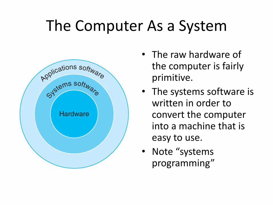
The Computer As a System
• The raw hardware of the computer is fairly primitive.
• The systems software is written in order to convert the computer into a machine that is easy to use.
• Note “systems programming”

RISC Design Strategies
• The basic RISC principle: “A simpler CPU is a faster CPU”.
• A number of the more common strategies include: • Fixed instruction length, generally one word (32 bits or 4
bytes). This simplifies instruction fetch. • Simplified and fewer addressing modes. • Fewer and simpler instructions in the instruction set. • Only load and store instructions access memory;
no add memory to register, add memory to memory, etc. • Let the compiler do it. Use a good compiler to break complex
high-level language statements into a number of simple assembly language statements.
RISC Design Principles
• Use optimizing compilers that issue simpler instructions. Complex compilers are easy to develop and test.
• Emphasize an ISA that allows simple and efficient instruction decoding.
• Operations that access memory should be minimized as memory access is a very time consuming operation.
• A simpler control unit, with little or no microcode, leads to a smaller unit. More chip area can be devoted to circuitry with significant “payback”, such as Level 1 cache.
The MIPS As An Example
• At the assembly language level, the MIPS is hard to program.
• This difficulty is due to techniques employed to speed up the pipelined CPU.
• The MIPS was designed to be programmed in high-level languages and present an interface designed for compilers.
• Only students program in assembly language.
The “Power Wall”
• In the early 2000’s there was a “sea change” in the design of computer chips.
• Design projections called for gradual increase in CPU clock rate to about 25 GHz by 2012.
• This has not happened, due to a problem that had not been considered significant.
• This problem is called the “power wall”. We now describe it.

CPU SPECINT Progress

What Happened in 2005?
• Here is a graph of the CPU clock rates and power use. All this power is emitted as heat.

The Power Wall

Response to the Power Wall
• Move to complex and costly cooling technologies. This is was IBM did for their large enterprise servers.
• Move to a multi-core design, each CPU chip comprises a number of simpler and smaller computing units, called “cores”. Each core is an independent CPU. The name choses avoids the name “multi-CPU CPU”.
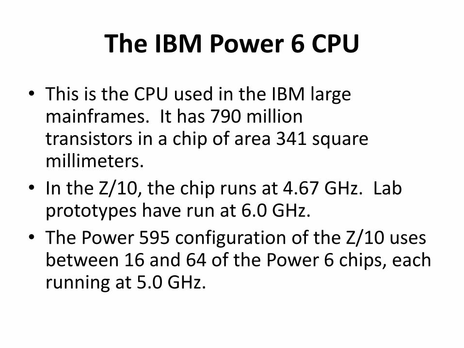
The IBM Power 6 CPU
• This is the CPU used in the IBM large mainframes. It has 790 million transistors in a chip of area 341 square millimeters.
• In the Z/10, the chip runs at 4.67 GHz. Lab prototypes have run at 6.0 GHz.
• The Power 595 configuration of the Z/10 uses between 16 and 64 of the Power 6 chips, each running at 5.0 GHz.
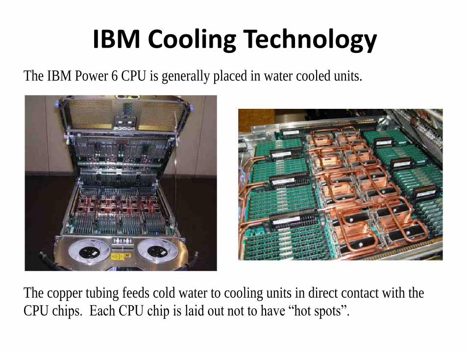
IBM Cooling Technology The IBM Power 6 CPU is generally placed in water cooled units.
The copper tubing feeds cold water to cooling units in direct contact with the
CPU chips. Each CPU chip is laid out not to have “hot spots”.
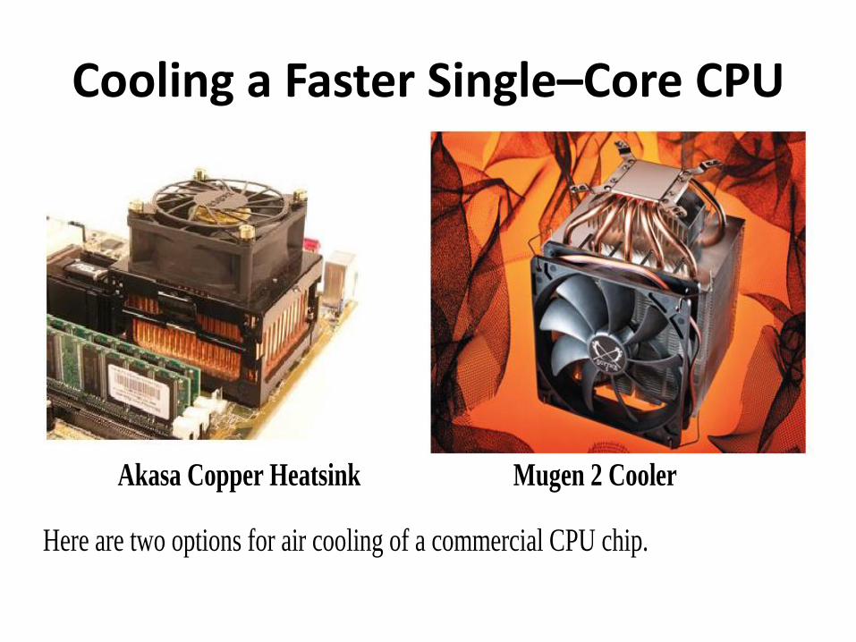
Cooling a Faster Single–Core CPU
Akasa Copper Heatsink Mugen 2 Cooler
Here are two options for air cooling of a commercial CPU chip.
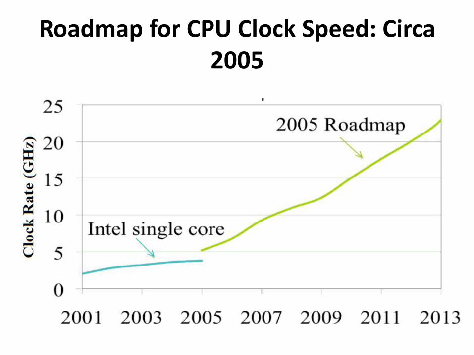
Roadmap for CPU Clock Speed: Circa 2005

Revised Clock Rate Projections
The Intel Prescott: The End of the Line • The CPU chip (code named “Prescott” by Intel) appears to be the high–
point in the actual clock rate. The fastest mass–produced chip ran at 3.8 GHz, though some enthusiasts (called “overclockers”) actually ran the chip at 8.0 GHz.
• Upon release, this chip was thought to generate about 40% more heat per clock cycle that earlier variants; thus the name “PresHot”. The heat problems could never be handled, and Intel abandoned the architecture.
• The Prescott idled at 50 degrees Celsius (122 degrees Fahrenheit) • The only way to keep it below 60 Celsius (140 F) was to operate it with
the cover off and plenty of ventilation. • Even equipped with the massive Akasa King Copper heat sink (see a
previous slide), the system reached 77 Celsius (171 F) when operating at 3.8 GHz under full load and shut itself down.

Intel’s Multicore Offerings for 2010

Intel’s Rationale
According to Intel, the multi–core technology will • permanently alter the course of computing as we know it, • provide new levels of energy efficient performance, • deliver full parallel execution of multiple software threads,
and • reduce the amount of electrical power to do the
computations.
• The current technology provides for one, two, four, or eight cores in a single processor.
• Intel expects to have available soon single processors with several tens of cores, if not one hundred.

Intel I7 Quad-Core