modeling and design of 3d imager ic - accueil - tel
TRANSCRIPT
HAL Id: tel-00795558https://tel.archives-ouvertes.fr/tel-00795558
Submitted on 28 Feb 2013
HAL is a multi-disciplinary open accessarchive for the deposit and dissemination of sci-entific research documents, whether they are pub-lished or not. The documents may come fromteaching and research institutions in France orabroad, or from public or private research centers.
L’archive ouverte pluridisciplinaire HAL, estdestinée au dépôt et à la diffusion de documentsscientifiques de niveau recherche, publiés ou non,émanant des établissements d’enseignement et derecherche français ou étrangers, des laboratoirespublics ou privés.
Modeling and design of 3D Imager ICVijayaragavan Viswanathan
To cite this version:Vijayaragavan Viswanathan. Modeling and design of 3D Imager IC. Other. Ecole Centrale de Lyon,2012. English. NNT : 2012ECDL0022. tel-00795558
ECOLE CENTRALE DE LYON
ECOLE DOCTORALE Electronique, Electrotechnique, Automatique
Institut des Nanotechnologies de Lyon
Année : 2012 Thèse Numero :
Thèse
pour obtenir le grade de
DOCTEUR DE L’ECOLE CENTRALE DE LYON
Discipline : Electronique
présentée et soutenue par
Vijayaragavan VISWANATHAN
le Jeudi 6 Septembre 2012
Modeling and design of 3D Imager IC
Thèse dirigée par Ian O’CONNOR
JURY :
Luc HEBRARD Professeur, InESS, Université de Strasbourg Président
Yusuf LEBLEBICI Professeur, Ecole Polytechnique Federale de Lausanne Rapporteur
Patrick GARDA Professeur, LIP6, Université Pierre et Marie Curie Rapporteur
Olivier LE BRIZ INGÉNIEUR, ST- Microelectronics Examinateur
Ian O’CONNOR Professeur, Ecole Centrale de Lyon Examinateur
David NAVARRO Maitre de Conference, Ecole Centrale de Lyon Examinateur
Lioua LABRAK Post-doctorant, Ecole Centrale de Lyon Examinateur


To my parents and my wifeTo my parents and my wifeTo my parents and my wifeTo my parents and my wife

i
Acknowledgement
I would like to first and foremost thank my advisor Professor Ian O’Connor for his invaluable
guidance, support, and for the encouragement he gave me during this thesis work. His valuable
support, insightful comments have made my Ph.D life very memorable and enjoyable. Not only did
he give me great advice for my research, but has been and is a great mentor for me. I truly appreciate
it. I am thankful for the precious time spent on reviewing this thesis.
I am grateful to Dr.David Navarro for being my associate advisor. I am thankful for all the
valuable time spend in discussion and to help me intellectually. I am grateful for the support he gave
in using different tools and sharing knowledge on image sensors. I also thank Dr.Lioua Labrak who
has been along with me all the time from the day I started the Ph.D. The numerous discussions and
sharing of knowledge have made me stronger in the subject. I would like to thank both of them for
reviewing this thesis.
I would like to show my gratitude for my colleagues at INL. I would especially like to thank
Felipe Frantz who is always willing to share his knowledge. I thank him for the support he rendered
all the time both at personal and professional level. I would also like to thank all the partners from
the 3D-IDEAS project for the support during this project. My time at INL has intellectually and
socially enriched by friends I have made. I thank all my former and current officemates Wan Du,
Zhenfu, Nanhao, Zhen Li, Mihai Galos, Jabeur Kotb, Nataliya and Bo Wang. I also thank Laurent
Carrel for the support. I would like to thank Patricia Dufaut, Nicole Durand, Sylvie Goncalves for
their administrative support and making my stay at INL a pleasant one.
I would like to thank my extended family which I am lucky enough to have during these
three years of stay in France. I am sure a word of thanks will not suffice for the amount of support
they have given me. Especially I am indebted to Mr &Mrs. Berlier, Agnes Prat, Jean Francois Prat
(Mamma & Pappa) and their family for making my stay a wonderful one. Ariane , Eric are one
another family which I cannot forget at all times of my life. Thanks a lot. Massimo, Andrea, Meng,
Aurelie, Remi, Jerome, Dawn, Franck, Peter, Pascale, Elisabeth, Joelle are few friends who made my
stay a wonderful one. I wish to thank all my Indian friends in Lyon for the support and fun times had
together. To name some of them Roy, Sudipta, Manjunath, Shwetha, Deepak, Preeti, Karthik. Thanks
all.

ii
Last but not the least, I owe my life to few people: Firstly, I would like to thank my better
half and my dear wife Mamatha for her understanding, belief and support all these years. I thank her
for being patient and supporting me all the time. I would like to thank my role model in life, my
father and mother. Thanks to all the sacrifice you have made all these years for me to come up in life.
I am here only because of them. I would like to thank my uncle and my all time support, Jayaraman
for his kind support and love. I owe a big thanks to my beloved sisters and my aunt for being always
with me. Also would like to thank all my in-laws who made my life a better one. To name a few
Anjanamurthy, Dhanalakshmi, Asha, Rupesh, Ajay, Deepu,Nirmala, Geetha and all their family.
I would like to say a special thank you to Ananthanarayanan, P.V.Gopi, Pallavi Reddy,
Jayakrishnan, Karthick , Anjali, Aparna ,Naga, Ganesh without whom I must have not decided to
pursue higher studies. Thanks to all!

iii
Abstract
CMOS image sensor based on Active pixel sensor has considerably contributed to the imaging
market and research interest in the past decade. Furthermore technology advancement has provided
the capability to integrate more and more functionality into a single chip in multiple layers leading to
a new paradigm, 3D integration. CMOS image sensor is one such application which could utilize the
capability of 3D stacked architecture to achieve dedicated technologies in different layers, wire
length reduction, less area, improved performances
This research work is focused mainly on the early stages of design space exploration using
hierarchical approach and aims at reducing time to market. This work investigates the imager from
the top-down design perspective. Methodical analysis of imager is performed to achieve high level of
flexibility and modularity. Re-useable models are developed to explore early design choices
throughout the hierarchy. Finally, pareto front (providing trade off solutions) methodology is applied
to explore the operating range of individual block at system level to help the designer making his
design choice. Furthermore the thermal issues which get aggravated in the 3D stacked chip on the
performance of the imager are studied.
SystemC based thermal model is built to investigate the behavior of imager pixel matrix and
to simulate the pixel matrix at high speed with acceptable accuracy compared to electrical
simulations. The modular nature of the model makes simulations with future matrix extension
straightforward. Validation of the thermal model with respect to electrical simulations is discussed.
Finally an integrated design flow is developed to perform 3D floorplanning and to perform thermal
analysis of the imager pixel matrix.
iv
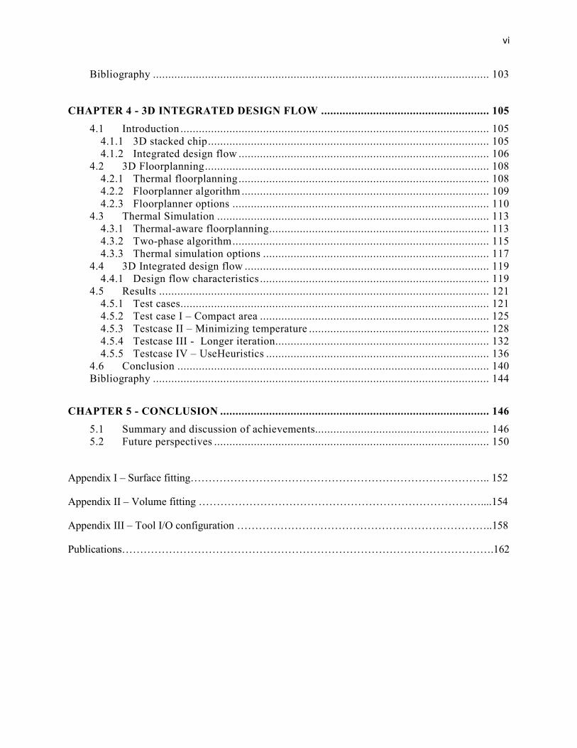
Contents
Acknowledgement…………………………………………………………………………….i
Abstract………………………………………………………………………………………iii
Contents………………………………………………………………………………………iv
List of Figures…………………………………………………….........................................vii
List of Tables…………………………………………………………………………………ix
Glossary……………………………………………………………………………………….x
CHAPTER 1 - INTRODUCTION ........................................................................................ 1
1.1 Imager ................................................................................................................. 1
1.1.1 The rise of the CMOS image sensor .................................................................. 3
1.1.2 CMOS Active Pixel Sensor ............................................................................... 4
1.1.3 CMOS image sensor performance metrics ......................................................... 5
1.1.4 CMOS image sensor noise ................................................................................ 6
1.2 3D technology ..................................................................................................... 8
1.2.1 Trend ............................................................................................................... 8
1.2.2 Opportunities ................................................................................................... 9
1.2.3 Issues ............................................................................................................. 13
1.2.4 3D Imager ...................................................................................................... 17
1.3 Research focus ................................................................................................... 17
1.3.1 Scalability - Technology ................................................................................. 17
1.3.2 Simulation scalability– Pixel matrix................................................................ 19
1.4 Key research contributions ................................................................................. 20
1.5 Thesis outline .................................................................................................... 21
Bibliography ............................................................................................................... 22
CHAPTER 2 - MODELING AND DESIGN .................................................................... 26
2.1 Introduction ....................................................................................................... 26
2.2 System description ............................................................................................. 27
2.2.1 Pixel matrix ................................................................................................... 27
2.2.2 ADC .............................................................................................................. 29
2.3 Methodology ..................................................................................................... 30
2.3.1 Modeling ....................................................................................................... 30
2.4 Parameter dependency graph .............................................................................. 34
2.4.1 Formulation ................................................................................................... 34
2.4.2 Frames per second (FPS) dependency graph .................................................... 36
2.4.3 Dynamic Range (DR) dependency graph ......................................................... 37
2.4.4 Signal to Noise Ratio (SNR) dependency graph .............................................. 38
v
2.5 Abstraction ........................................................................................................ 39
2.5.1 Segregation of abstractions ............................................................................. 39
2.5.2 Formulation ................................................................................................... 41
2.6 Results .............................................................................................................. 42
2.6.1 Pixel matrix ................................................................................................... 42
2.6.1.1 System level ............................................................................................ 42
2.6.1.2 Behavioral level ...................................................................................... 43
2.6.1.3 Accurate behavioral level ........................................................................ 45
2.6.2 ADC - Results ................................................................................................ 46
2.6.2.1 System level ............................................................................................ 47
2.6.2.2 Behavioral level – DAC .......................................................................... 50
2.6.2.3 Behavioral level - Comparator ................................................................. 51
2.7 Pareto-front methodology ................................................................................... 53
2.7.1 Methodology .................................................................................................. 54
2.7.2 Pixel pareto-front - Results ............................................................................ 55
2.8 Conclusion ........................................................................................................ 58
Bibliography ................................................................................................................ 60
CHAPTER 3 - THERMAL-AWARE IMAGE SENSOR MODEL .................................. 62
3.1 Introduction ....................................................................................................... 62
3.2 Thermal Model .................................................................................................. 63
3.2.1 Problems and requirements ............................................................................. 63
3.2.2 Compact thermal model .................................................................................. 64
3.2.3 Model development steps ............................................................................... 65
3.3 Exhaustive data generation ................................................................................. 67
3.3.1 Pixel behavior ................................................................................................ 67
3.3.2 Imager thermal model ..................................................................................... 68
3.3.3 Electrical simulations ..................................................................................... 69
3.4 Fitting ............................................................................................................... 71
3.4.1 Types of fitting .............................................................................................. 71
3.4.2 Surface fitting ................................................................................................ 72
3.4.3 Volume fitting ................................................................................................ 74
3.5 Pre-Validation ................................................................................................... 77
3.5.1 Requirement ................................................................................................... 77
3.5.2 Preliminary results ......................................................................................... 79
3.5.3 Fitting order accuracy ..................................................................................... 81
3.6 Integrated simulation environment ..................................................................... 87
3.6.1 SystemC......................................................................................................... 87
3.6.2 Image processing ............................................................................................ 88
3.6.3 SystemC-based pixel matrix model ................................................................. 89
3.6.4 Model integration ........................................................................................... 91
3.6.5 Simulation speed ............................................................................................ 91
3.7 Post-validation ................................................................................................... 94
3.7.1 Matrix simulation ........................................................................................... 94
3.7.2 Test case I (128*128 “lena”) ........................................................................... 95
3.7.3 Test case II (256*256 lena) ............................................................................. 97
3.7.4 Test case III (White picture) ........................................................................... 99
3.8 Inference ......................................................................................................... 102
vi
Bibliography .............................................................................................................. 103
CHAPTER 4 - 3D INTEGRATED DESIGN FLOW ....................................................... 105
4.1 Introduction ..................................................................................................... 105
4.1.1 3D stacked chip ............................................................................................ 105
4.1.2 Integrated design flow .................................................................................. 106
4.2 3D Floorplanning ............................................................................................. 108
4.2.1 Thermal floorplanning .................................................................................. 108
4.2.2 Floorplanner algorithm ................................................................................. 109
4.2.3 Floorplanner options .................................................................................... 110
4.3 Thermal Simulation ......................................................................................... 113
4.3.1 Thermal-aware floorplanning ........................................................................ 113
4.3.2 Two-phase algorithm .................................................................................... 115
4.3.3 Thermal simulation options .......................................................................... 117
4.4 3D Integrated design flow ................................................................................ 119
4.4.1 Design flow characteristics ........................................................................... 119
4.5 Results ............................................................................................................ 121
4.5.1 Test cases ..................................................................................................... 121
4.5.2 Test case I – Compact area ........................................................................... 125
4.5.3 Testcase II – Minimizing temperature ........................................................... 128
4.5.4 Testcase III - Longer iteration ...................................................................... 132
4.5.5 Testcase IV – UseHeuristics ......................................................................... 136
4.6 Conclusion ...................................................................................................... 140
Bibliography .............................................................................................................. 144
CHAPTER 5 - CONCLUSION ........................................................................................ 146
5.1 Summary and discussion of achievements......................................................... 146
5.2 Future perspectives .......................................................................................... 150
Appendix I – Surface fitting……………………………………………………………………….. 152
Appendix II – Volume fitting ……………………………………………………………………....154
Appendix III – Tool I/O configuration ……………………………………………………………..158
Publications………………………………………………………………………………………….162
vii
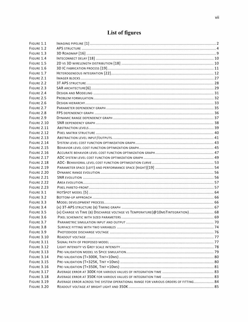
List of figures
FIGURE 1.1 IMAGING PIPELINE [1] ............................................................................................................ 2 FIGURE 1.2 APS STRUCTURE ................................................................................................................... 4
FIGURE 1.3 3D ROADMAP [16] ............................................................................................................... 9
FIGURE 1.4 INTECONNECT DELAY [18] ..................................................................................................... 10
FIGURE 1.5 2D VS 3D WIRELENGTH DISTRIBUTION [18] ............................................................................... 10 FIGURE 1.6 3D IC FABRICATION PROCESS [19] ........................................................................................... 11
FIGURE 1.7 HETEROGENEOUS INTEGRATION [22] ........................................................................................ 12
FIGURE 2.1 IMAGER BLOCKS .................................................................................................................. 27 FIGURE 2.2 3T APS STRUCTURE ............................................................................................................. 28
FIGURE 2.3 SAR ARCHITECTURE[6] ......................................................................................................... 29
FIGURE 2.4 DESIGN AND MODELING ....................................................................................................... 31
FIGURE 2.5 PROBLEM FORMULATION ....................................................................................................... 32 FIGURE 2.6 DESIGN HIERARCHY .............................................................................................................. 33
FIGURE 2.7 PARAMETER DEPENDENCY GRAPH ............................................................................................ 35
FIGURE 2.8 FPS DEPENDENCY GRAPH ...................................................................................................... 36 FIGURE 2.9 DYNAMIC RANGE DEPENDENCY GRAPH ...................................................................................... 37
FIGURE 2.10 SNR DEPENDENCY GRAPH ..................................................................................................... 38
FIGURE 2.11 ABSTRACTION LEVELS ........................................................................................................... 39
FIGURE 2.12 PIXEL MATRIX STRUCTURE ..................................................................................................... 40 FIGURE 2.13 ABSTRACTION LEVEL INPUT/OUTPUTS. ...................................................................................... 41
FIGURE 2.14 SYSTEM LEVEL COST FUNCTION OPTIMIZATION GRAPH ................................................................... 43
FIGURE 2.15 BEHAVIOR LEVEL COST FUNCTION OPTIMIZATION GRAPH ................................................................ 45
FIGURE 2.16 ACCURATE BEHAVIOR LEVEL COST FUNCTION OPTIMIZATION GRAPH .................................................. 47 FIGURE 2.17 ADC SYSTEM LEVEL COST FUNCTION OPTIMIZATION GRAPH ............................................................ 49
FIGURE 2.18 ADC- BEHAVIORAL LEVEL COST FUNCTION OPTIMIZATION CURVE ..................................................... 53
FIGURE 2.19 PARAMETER SPACE (LEFT) AND PERFORMANCE SPACE (RIGHT)[19] .................................................. 54 FIGURE 2.20 DYNAMIC RANGE EVOLUTION ................................................................................................. 56
FIGURE 2.21 SNR EVOLUTION ................................................................................................................ 56
FIGURE 2.22 AREA EVOLUTION ................................................................................................................ 57
FIGURE 2.23 PIXEL PARETO-FRONT ........................................................................................................... 57 FIGURE 3.1 HOTSPOT MODEL [5] ........................................................................................................... 64
FIGURE 3.2 BOTTOM-UP APPROACH ........................................................................................................ 66
FIGURE 3.3 MODEL DEVELOPMENT PROCESS .............................................................................................. 66
FIGURE 3.4 (A) 3T-APS STRUCTURE (B) TIMING GRAPH ............................................................................... 67 FIGURE 3.5 (A) CHARGE VS TIME (B) DISCHARGE VOLTAGE VS TEMPERATURE(@10MSTINTEGRATION) ..................... 68
FIGURE 3.6 PIXEL SCHEMATIC WITH SIZED PARAMETERS ............................................................................... 69
FIGURE 3.7 PARAMETRIC SIMULATION INPUT AND OUTPUT ........................................................................... 70 FIGURE 3.8 SURFACE FITTING WITH TWO VARIABLES ................................................................................... 74
FIGURE 3.9 PHOTODIODE DISCHARGE VOLTAGE ......................................................................................... 76
FIGURE 3.10 READOUT VOLTAGE ............................................................................................................. 77
FIGURE 3.11 SIGNAL PATH OF PROPOSED MODEL ......................................................................................... 77 FIGURE 3.12 LIGHT INTENSITY VS GREY SCALE INTENSITY ................................................................................ 78
FIGURE 3.13 PRE-VALIDATION MODEL VS SPICE SIMULATION ........................................................................... 79
FIGURE 3.14 PRE-VALIDATION (T=300K, TINT=10MS) ................................................................................. 80
FIGURE 3.15 PRE-VALIDATION (T=325K, TINT =10MS) ................................................................................ 80 FIGURE 3.16 PRE-VALIDATION (T=350K, TINT =10MS) ................................................................................ 81
FIGURE 3.17 AVERAGE ERROR AT 300K FOR VARIOUS VALUES OF INTEGRATION TIME ............................................ 83
FIGURE 3.18 AVERAGE ERROR AT 350K FOR VARIOUS VALUES OF INTEGRATION TIME ............................................ 83 FIGURE 3.19 AVERAGE ERROR ACROSS THE SYSTEM OPERATIONAL RANGE FOR VARIOUS ORDERS OF FITTING ................. 84
FIGURE 3.20 READOUT VOLTAGE AT BRIGHT LIGHT AND 350K ......................................................................... 85
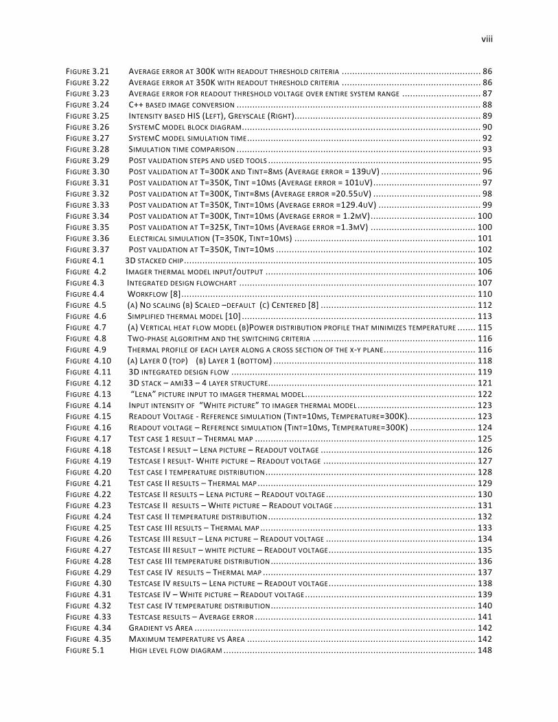
viii
FIGURE 3.21 AVERAGE ERROR AT 300K WITH READOUT THRESHOLD CRITERIA ..................................................... 86
FIGURE 3.22 AVERAGE ERROR AT 350K WITH READOUT THRESHOLD CRITERIA ..................................................... 86 FIGURE 3.23 AVERAGE ERROR FOR READOUT THRESHOLD VOLTAGE OVER ENTIRE SYSTEM RANGE .............................. 87
FIGURE 3.24 C++ BASED IMAGE CONVERSION ............................................................................................. 88
FIGURE 3.25 INTENSITY BASED HIS (LEFT), GREYSCALE (RIGHT)....................................................................... 89
FIGURE 3.26 SYSTEMC MODEL BLOCK DIAGRAM........................................................................................... 90 FIGURE 3.27 SYSTEMC MODEL SIMULATION TIME ......................................................................................... 92
FIGURE 3.28 SIMULATION TIME COMPARISON ............................................................................................. 93
FIGURE 3.29 POST VALIDATION STEPS AND USED TOOLS ................................................................................. 95
FIGURE 3.30 POST VALIDATION AT T=300K AND TINT=8MS (AVERAGE ERROR = 139UV) ...................................... 96 FIGURE 3.31 POST VALIDATION AT T=350K, TINT =10MS (AVERAGE ERROR = 101UV) ......................................... 97
FIGURE 3.32 POST VALIDATION AT T=300K, TINT=8MS (AVERAGE ERROR =20.55UV) ......................................... 98
FIGURE 3.33 POST VALIDATION AT T=350K, TINT=10MS (AVERAGE ERROR =129.4UV) ....................................... 99 FIGURE 3.34 POST VALIDATION AT T=300K, TINT=10MS (AVERAGE ERROR = 1.2MV) ........................................ 100
FIGURE 3.35 POST VALIDATION AT T=325K, TINT=10MS (AVERAGE ERROR =1.3MV) ........................................ 100
FIGURE 3.36 ELECTRICAL SIMULATION (T=350K, TINT=10MS) ..................................................................... 101
FIGURE 3.37 POST VALIDATION AT T=350K, TINT=10MS ............................................................................ 102
FIGURE 4.1 3D STACKED CHIP ............................................................................................................... 105
FIGURE 4.2 IMAGER THERMAL MODEL INPUT/OUTPUT ................................................................................ 106
FIGURE 4.3 INTEGRATED DESIGN FLOWCHART .......................................................................................... 107
FIGURE 4.4 WORKFLOW [8] ................................................................................................................ 110 FIGURE 4.5 (A) NO SCALING (B) SCALED –DEFAULT (C) CENTERED [8] ........................................................... 112
FIGURE 4.6 SIMPLIFIED THERMAL MODEL [10] ......................................................................................... 113
FIGURE 4.7 (A) VERTICAL HEAT FLOW MODEL (B)POWER DISTRIBUTION PROFILE THAT MINIMIZES TEMPERATURE ....... 115 FIGURE 4.8 TWO-PHASE ALGORITHM AND THE SWITCHING CRITERIA .............................................................. 116
FIGURE 4.9 THERMAL PROFILE OF EACH LAYER ALONG A CROSS SECTION OF THE X-Y PLANE. .................................. 116
FIGURE 4.10 (A) LAYER 0 (TOP) (B) LAYER 1 (BOTTOM) ............................................................................. 118
FIGURE 4.11 3D INTEGRATED DESIGN FLOW ............................................................................................. 119 FIGURE 4.12 3D STACK – AMI33 – 4 LAYER STRUCTURE............................................................................... 121
FIGURE 4.13 “LENA” PICTURE INPUT TO IMAGER THERMAL MODEL ................................................................. 122
FIGURE 4.14 INPUT INTENSITY OF “WHITE PICTURE” TO IMAGER THERMAL MODEL ............................................. 123 FIGURE 4.15 READOUT VOLTAGE - REFERENCE SIMULATION (TINT=10MS, TEMPERATURE=300K).......................... 123
FIGURE 4.16 READOUT VOLTAGE – REFERENCE SIMULATION (TINT=10MS, TEMPERATURE=300K) ......................... 124
FIGURE 4.17 TEST CASE 1 RESULT – THERMAL MAP .................................................................................... 125
FIGURE 4.18 TESTCASE I RESULT – LENA PICTURE – READOUT VOLTAGE ........................................................... 126 FIGURE 4.19 TESTCASE I RESULT- WHITE PICTURE – READOUT VOLTAGE .......................................................... 127
FIGURE 4.20 TEST CASE I TEMPERATURE DISTRIBUTION ................................................................................ 128
FIGURE 4.21 TEST CASE II RESULTS – THERMAL MAP ................................................................................... 129
FIGURE 4.22 TESTCASE II RESULTS – LENA PICTURE – READOUT VOLTAGE ......................................................... 130 FIGURE 4.23 TESTCASE II RESULTS – WHITE PICTURE – READOUT VOLTAGE ...................................................... 131
FIGURE 4.24 TEST CASE II TEMPERATURE DISTRIBUTION ............................................................................... 132
FIGURE 4.25 TEST CASE III RESULTS – THERMAL MAP .................................................................................. 133 FIGURE 4.26 TESTCASE III RESULT – LENA PICTURE – READOUT VOLTAGE ......................................................... 134
FIGURE 4.27 TESTCASE III RESULT – WHITE PICTURE – READOUT VOLTAGE ........................................................ 135
FIGURE 4.28 TEST CASE III TEMPERATURE DISTRIBUTION .............................................................................. 136
FIGURE 4.29 TEST CASE IV RESULTS – THERMAL MAP ................................................................................. 137 FIGURE 4.30 TESTCASE IV RESULTS – LENA PICTURE – READOUT VOLTAGE ........................................................ 138
FIGURE 4.31 TESTCASE IV – WHITE PICTURE – READOUT VOLTAGE ................................................................. 139
FIGURE 4.32 TEST CASE IV TEMPERATURE DISTRIBUTION .............................................................................. 140
FIGURE 4.33 TESTCASE RESULTS – AVERAGE ERROR .................................................................................... 141 FIGURE 4.34 GRADIENT VS AREA ........................................................................................................... 142
FIGURE 4.35 MAXIMUM TEMPERATURE VS AREA ....................................................................................... 142
FIGURE 5.1 HIGH LEVEL FLOW DIAGRAM ................................................................................................ 148
ix
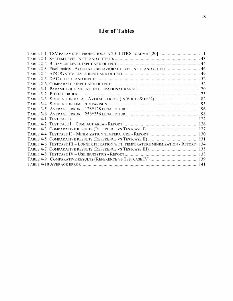
List of Tables
TABLE 1-1 TSV PARAMETER PROJECTIONS IN 2011 ITRS ROADMAP[20] ................................. 11
TABLE 2-1 SYSTEM LEVEL INPUT AND OUTPUTS ..................................................................... 43
TABLE 2-2 BEHAVIOR LEVEL INPUT AND OUTPUT ................................................................... 44
TABLE 2-3 Pixel matrix - ACCURATE BEHAVIORAL LEVEL INPUT AND OUTPUT .......................... 46
TABLE 2-4 ADC SYSTEM LEVEL INPUT AND OUTPUT .............................................................. 49
TABLE 2-5 DAC OUTPUT AND INPUTS ................................................................................... 52
TABLE 2-6 COMPARATOR INPUT AND OUTPUTS ...................................................................... 52
TABLE 3-1 PARAMETRIC SIMULATION OPERATIONAL RANGE ................................................... 70
TABLE 3-2 FITTING ORDER ................................................................................................... 75
TABLE 3-3 SIMULATION DATA – AVERAGE ERROR (IN VOLTS & IN %) ..................................... 82
TABLE 3-4 SIMULATION TIME COMPARISON ........................................................................... 93
TABLE 3-5 AVERAGE ERROR – 128*128 LENA PICTURE .......................................................... 96
TABLE 3-6 AVERAGE ERROR – 256*256 LENA PICTURE .......................................................... 98
TABLE 4-1 TEST CASES ...................................................................................................... 122
TABLE 4-2 TEST CASE I – COMPACT AREA - REPORT ............................................................ 126
TABLE 4-3 COMPARATIVE RESULTS (REFERENCE VS TESTCASE I) .......................................... 127
TABLE 4-4 TESTCASE II – MINIMIZATION TEMPERATURE - REPORT ....................................... 130
TABLE 4-5 COMPARATIVE RESULTS (REFERENCE VS TESTCASE II) ........................................ 131
TABLE 4-6 TESTCASE III – LONGER ITERATION WITH TEMPERATURE MINIMIZATION - REPORT . 134
TABLE 4-7 COMPARATIVE RESULTS (REFERENCE VS TESTCASE III) ....................................... 135
TABLE 4-8 TESTCASE IV – USEHEURISTICS - REPORT ........................................................... 138
TABLE 4-9 COMPARATIVE RESULTS (REFERENCE VS TESTCASE IV) ...................................... 139
TABLE 4-10 AVERAGE ERROR .............................................................................................. 141

x
Glossary
CMOS Complimentary Metal Oxide Semiconductor
CISs CMOS Image Sensors
APS Active Pixel Sensor
ADC Analog-to-Digital Conversion
CCDs- Charged Coupled Devices
CDS - Correlated Double Sampling
ISP Image Signal Processor
ENOB Effective Number Of Bits
FPN Fixed Pattern Noise
MOS Metal-Oxide-Semiconductor
MSB Most Significant Bit
PPS Passive Pixel Sensor
PRNU Photo Response Non-Uniformity
QE Quantum Effciency
SNR Signal-to-Noise Ratio
RAM Random Access Memory
SF Source Follower
AMS Austria Micro Systems
MP MegaPixel
DR Dynamic Range
SNR Signal to Noise ration
FPS Frames Per Second
FF Fill factor
3D-IC Three-Dimensional Integrated Circuit

xi
Chapter 1 Introduction
In the past decade, semiconductor companies around the world started investing in the area of
image sensors. On the technology point of view, CMOS Image Sensors (CIS) have become
mature and attractive to produce in mass quantities. On the application point of view, CIS and
its capability is utilized in various sectors pertaining to various application areas such as:
commercial applications (toys, digital cameras, web cameras etc.), industrial sector (machine
vision, automotive, quality control etc.), security sector (security cameras, motion detection,
finger print ID, target tracking, spy cameras etc.) and it is also used in space applications. On
the business point of view, the know-how in the IC design and fabrication process has increase
the chance to be successful and meet the market demand on large array formats, high image
quality, low cost, low power. Current technology advancement i.e 3D technology has
advantage of small foot print imagers, dedicated technology (analog, digital etc.) for different
layers is becoming more and more attractive because of cost and optimized performance. In
this research work we will focus on the 3D imager IC.
In the section 1.1 we will see how an imager functions, the rise of CIS technology,
CMOS APS structure, CIS performance metrics, CIS noise sources. Section 1.2 describes in
detail the 3D technology trend, opportunities and issues. Section 1.3 describes in detail the
research focus and followed by research contribution in section 1.4 and finally thesis outline is
described in section 1.5.
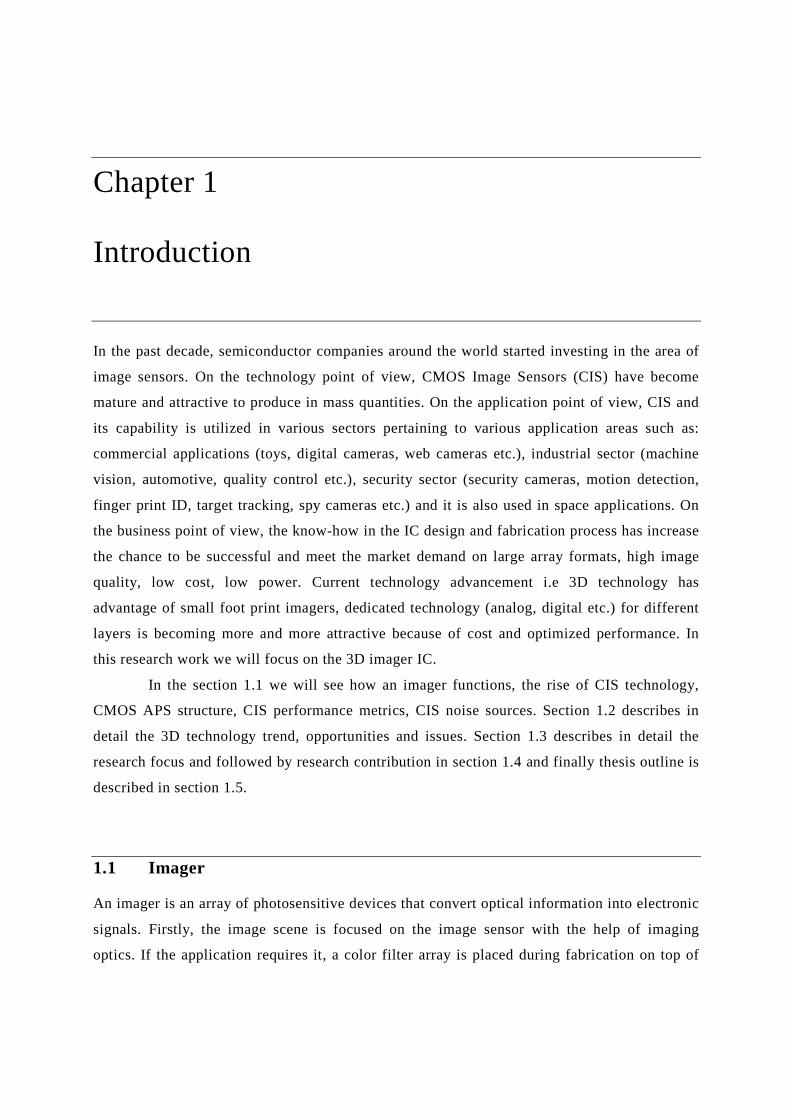
1.1 Imager An imager is an array of photosensitive devices that convert optical information into electronic
signals. Firstly, the image scene is focused on the image sensor with the help of imaging
optics. If the application requires it, a color filter array is placed during fabrication on top of
2
Chapter 1 – Introduction the image sensor arrays for color sensing. Because of the color filter, each pixel behind the
filter array produces an electrical signal corresponding to one single color (red, green or blue).
An analog-to-digital converter (ADC) is used to convert the generated signal into the digital
domain for digital post processing such as color processing, image enhancement, data
compression for storage, etc. The digital image data after the ADC block can also be fed back
for auto exposure and auto focus followed by (Image Signal Processor) ISP for processing ,
color enhancement etc. as shown in Figure 1.1.
Visible spectrum imaging is the main target for consumer applications such as mobile
phone cameras. Silicon, the cheap and widely-available material at the basis of the
semiconductor industry, also happens to be highly suitable for visible spectrum imaging due to
its high absorption in the visible range of light (i.e. the range of wavelengths over which the
human eye is sensitive, around 390nm-750nm).
In the following sections, we focus on the drive behind the main (CMOS)
technological implementation of consumer image sensors, and on the main performance
metrics and limitations.
Figure 1.1 Imaging pipeline [1]

3
Chapter 1 – Introduction 1.1.1 The rise of the CMOS image sensor
Over the past decade, developments in image sensor technology have brought a shift from
Charge Coupled Devices (CCD) to Complementary Metal Oxide Semiconductor (CMOS)
based image sensor technology, due to the potential of CMOS imager sensors (CIS) compared
to CCD. In this research work, we focus exclusively on CIS. Some key advantages of the CIS
technology are listed below:
Low power dissipation
CIS has lower voltage swing, switching frequency and capacitance which allows
them to be more suitable for portable applications [2].
Integration and miniaturization
CMOS components such as memory, signal processing circuits, microprocessors
can be integrated into the same chip. This reduces complexity in board or System in
Package (SiP) design and reduces the cost of the system [3].
Cheaper fabrication
CIS are produced for several years by tweaking the standard digital CMOS
processes[4][5]. This supports mass production using existing CMOS fabrication
lines, reducing the cost of production. Lately, as the scaling continues these tweakss
have become more pronounced and lead today to dedicated production lines to
tackle technology scaling and market demand.
Reliability
Due to on-chip integration, the component count for assembly of the overall system
is reduced, which improves robustness and reliability. Of course, scaling can tend to
offset this advantage since the reliability of the individual circuit elements is
reduced.
Speed
On-chip integration of all components lowers interconnect RC time constants
between them, and therefore favors increases to the rate of data transfer between the
sensor and the processing units. This translates into faster frame rates: CIS with
rates of 10,000 frames per second has been reported [6]. Normal commercial
sensors work at few hundreds of frames per second.
4
Chapter 1 – Introduction
Random access
With the CIS, because of its two-dimensional structure of the data readout circuit
within the imaging sensor, which allows for data readout by selectively addressing
X and Y coordinates, it is relatively easy to realize a random-access [7]
performance.
Although CIS provides the above advantages it suffers from noise and lower
sensitivity compared to CCD technology. Higher fixed pattern noise [8] is observed due to the
readout through a chain of buffers and amplifiers. These drawbacks are reduced with
technology improvements and the emergence of dedicated CMOS production lines for image
sensor fabrication.
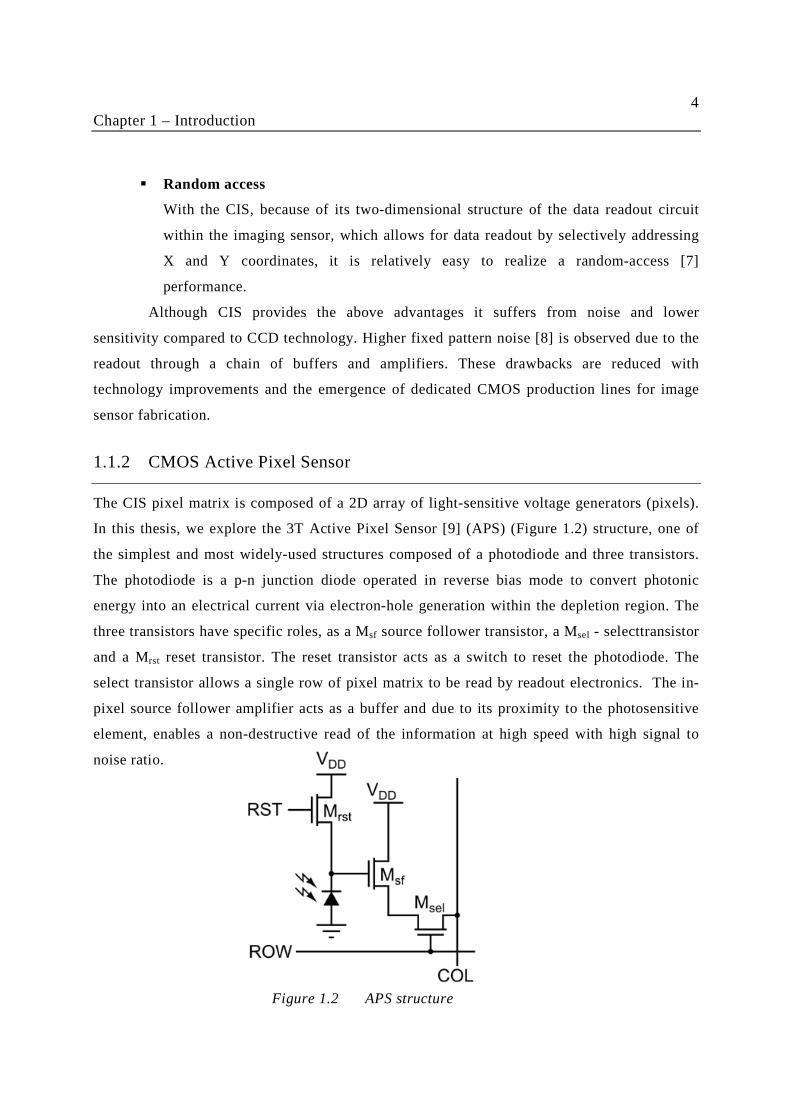
1.1.2 CMOS Active Pixel Sensor
The CIS pixel matrix is composed of a 2D array of light-sensitive voltage generators (pixels).
In this thesis, we explore the 3T Active Pixel Sensor [9] (APS) (Figure 1.2) structure, one of
the simplest and most widely-used structures composed of a photodiode and three transistors.
The photodiode is a p-n junction diode operated in reverse bias mode to convert photonic
energy into an electrical current via electron-hole generation within the depletion region. The
three transistors have specific roles, as a Msf source follower transistor, a Msel - selecttransistor
and a Mrst reset transistor. The reset transistor acts as a switch to reset the photodiode. The
select transistor allows a single row of pixel matrix to be read by readout electronics. The in-
pixel source follower amplifier acts as a buffer and due to its proximity to the photosensitive
element, enables a non-destructive read of the information at high speed with high signal to
noise ratio.
Figure 1.2 APS structure
5
Chapter 1 – Introduction
However, the presence of three transistors in each pixel leads to a low overall pixel
fill factor, which persists even though technology scaling reduces transistor sizes. Detailed
operation of APS architecture is described in the following chapters.
1.1.3 CMOS image sensor performance metrics
The performance of an APS structure is measured with a number of criteria: Few of them are
described in the following paragraphs:
Dynamic range: the range between the minimum and maximum detectable illumination
levels, measured in dB. The dynamic range can also be represented as the number of
illumination levels that can be encoded. When the incident illumination is high, the
photocurrent is large, causing the photodiode to discharge quickly. Therefore, it is
necessary to reduce the integration time in order to prevent the pixel from discharging
completely. However, in low illumination, the photocurrent is small, causing the
photodiode to discharge slowly. In this case, it would be necessary to increase the
integration time in order to allow the photodiode to discharge enough to provide a
detectable signal at the output.
dB
σonTintegrati*Idark*q
1
onTintegrati
q
IdarkonTintegrati
qQmax
20logIminImax
20logD.R2
r
1010
+
−==
--(1.1)
where Qmax is full well capacity, Idark is the dark current, Tintegration is integration time
and σr is read out noise.
The dynamic range of a 3T-APS is determined by the voltage swing between
the power supply voltage (VDD) and the ground voltage. However, the threshold voltage
drop across the source follower diminishes the voltage detection range at the output.
Also, technology scaling reduces the supply voltage (and to a lesser extent the threshold
voltage), which affects the dynamic range.
Frame rate: is used to describe the imaging speed of the sensor. Normally it refers to
the number of images that can be taken within a second.
6
Chapter 1 – Introduction
Sensitivity describes the output response of the photo sensor as a function of light
intensity at specific wavelength. Sensitivity is the ratio of collected charges to the
number of incident photons.
Conversion gain: After the photons are converted and collected at pixel floating
diffusion (FD) nodes, collected electrons cause a proportional change in voltage
depending on the FD node capacitance. This is called charge to voltage conversion
gain.
Signal to noise ratio: the ratio of signal power to noise power, measured in dB. SNR
can be improved by improving the signal, which provides a better signal dynamic.
dB)σegrationIdark)Tint(I
q1
(onTintegrati
q
I10log)SNR(I
2rph2
2
2ph
10ph
++=
--(1.2)
where Iph is photocurrent signal, Idark is the dark current, Tintegration is integration time
and σr is read out noise. The following section describes in detail the sources of noise in
CMOS APS structure.
1.1.4 CMOS image sensor noise
Like any other electronic circuit, CMOS image sensor also suffers from noise. There are two
primary sources of noise [10][11][48] in CMOS APS. They are
• Temporal noise
• Fixed pattern noise (FPN)
Temporal noise
Temporal noise is temporally random and not constant from frame to frame. It is described by
statistical distributions and can be reduced by averaging successive frames or by using
correlated double sampling techniques. In general temporal noise can be divided into three
categories: shot noise, 1/f noise and reset noise
7
Chapter 1 – Introduction
Photon shot noise: Photon shot noise describes the fundamental statistical uncertainty
on the amount of photoelectrons that are generated by light falling on the photodiode.
It depends on fundamental physical laws, little impact from the design decisions.
1/f noise: originates from fluctuation in the conductivity. In CMOS APS different
components contribute to total 1/f noise at different operation phases. For example
during integration time, this noise is produced by photodiode dark current fluctuation.
During readout phase, the column source follower and access transistor generate 1/f
noise. In system level, reducing the system temperature helps in improving 1/f noise.
Reset noise: The photo-generated electrons start to accumulate on the junction
capacitor after the reset operation. Reset noise is a function of sensor temperature and
capacitance. It causes variance in the voltage to which the photodiode is charged.
= --(1.3)
where K is the Boltzmann constant, T is the temperature (Kelvins).
Fixed pattern noise
Fixed pattern noise (FPN)[8] is a spatial noise. It is the variation of output from different
pixels under the same illumination conditions. It produces variations from pixel to pixel or
column to column in the sensor array. The FPN could be due to non-uniformity of the micro-
lens, non-uniformity in effective pixel fill factor (variability in pixel circuit dimensions) or
non-uniformity in conversion gain (variability in transistor characteristics). FPN can be
categorized principally by the signal dependence. Signal independent one is the Dark Signal
Non-Uniformity (DSNU) and signal dependent one is Photo Response Non-Uniformity
(PRNU).
Dark Signal Non-Uniformity (DSNU): Pixel to pixel dark current variation is one of
the sources of FPN. This variation is not signal dependent. It is due to non-uniform
spatial patterns of impurity concentrations in the wafer. Additionally, this non-
uniformity depends on temperature distribution on the pixel array.
8
Chapter 1 – Introduction
Photo Response Non Uniformity (PRNU): This is signal dependent component of
FPN. Local variation in different layer thickness and doping impurities cause
variations in photo generated carrier lifetime. These are caused by mask
misalignment. They result in modifications of quantum efficiency, source follower
gain or pixel capacitance across the pixel array. PRNU depends on process
technology, light spectrum, pixel design and timing.
Existing conventional 2D image sensor suffers from many limitations. The main
drawback is the limited area available to accommodate the pixel array and other blocks (ADC,
ISP etc.) together. Due to this reason fill factor of pixel is reduced. 2D image sensor blocks are
connected by long wires increasing the RC delay and reducing the bandwidth. The entire chip
is fabricated using single technology. These drawbacks are overcome by the 3D imagers. The
main drivers for 3D technology are imagers and memories [13][14]. 3D imager has shorter
wirelength and so increased bandwidth. Long term goal of 3D imager is the possibility of
increasing the fill factor and increasing the local image processing by stacking pixels above
transistors (APS transistors underneath photodiode). But the intermediate term and high
granularity approach is to have an image processing block below pixel matrix. This is very
attractive due to the technology heterogeneity (using different technology node for each layer
and dedicated CMOS imager process lines). 3D stacking would free CMOS imager processes
completely from standard digital.
During this research work we will focus on how we can model and design an imager
using the 3D technology. Due importance is given to analyzing the problems when moving to
3D and proposed solutions to overcome the associated (mainly thermal) issues.
1.2 3D technology
1.2.1 Trend
In 1965, Gordon Moore postulated his famous and eponymous law, which formalized for the
first time scaling trends in the semiconductor industry, trends which continue to this day.
However, at the end of the 20th century, the semiconductor industry started slowing from the
9
Chapter 1 – Introduction trend proposed by the law, and costly technological solutions (e.g. copper interconnect, high-k
dielectrics) became increasingly necessary to continue to achieve the levels of performance
predicted by Moore's Law. Recently, the concept of 3D integration and use of the vertical
dimension as a vector to pursue performance began to gather support in both academic and
industrial communities [15][16]. The idea was in fact originated in 1985 by the Nobel laureate
Richard Feynman, who expressed the idea of stacking in his address on “Computing machines
in the future”. Today, it is widely accepted that 3D integration is well on its way to becoming a
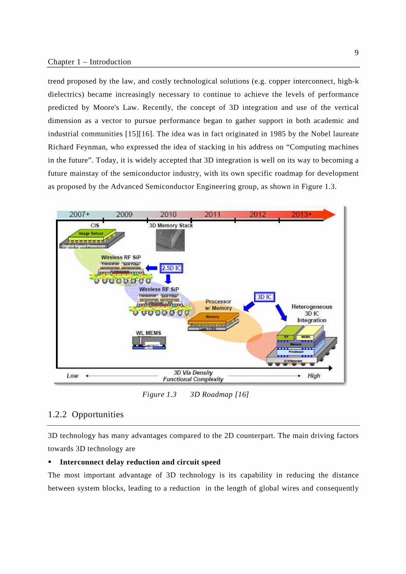
future mainstay of the semiconductor industry, with its own specific roadmap for development
as proposed by the Advanced Semiconductor Engineering group, as shown in Figure 1.3.
1.2.2 Opportunities
3D technology has many advantages compared to the 2D counterpart. The main driving factors
towards 3D technology are
Interconnect delay reduction and circuit speed
The most important advantage of 3D technology is its capability in reducing the distance
between system blocks, leading to a reduction in the length of global wires and consequently
Figure 1.3 3D Roadmap [16]
10
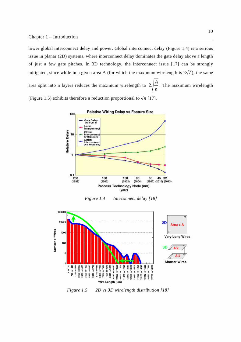
Chapter 1 – Introduction lower global interconnect delay and power. Global interconnect delay (Figure 1.4) is a serious
issue in planar (2D) systems, where interconnect delay dominates the gate delay above a length
of just a few gate pitches. In 3D technology, the interconnect issue [17] can be strongly
mitigated, since while in a given area A (for which the maximum wirelength is 2√), the same
area split into n layers reduces the maximum wirelength to n
A2 . The maximum wirelength
(Figure 1.5) exhibits therefore a reduction proportional to √ [17].
Figure 1.4 Inteconnect delay [18]
Figure 1.5 2D vs 3D wirelength distribution [18]
11
Chapter 1 – Introduction
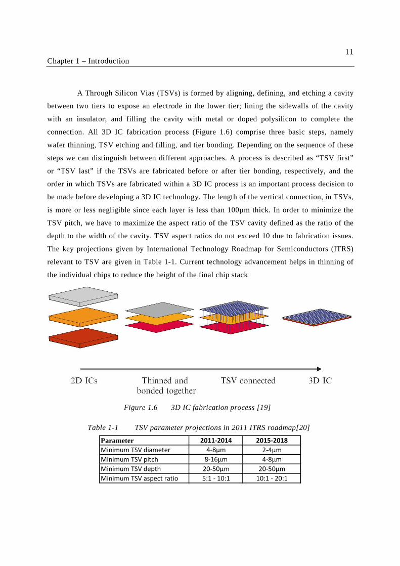
A Through Silicon Vias (TSVs) is formed by aligning, defining, and etching a cavity
between two tiers to expose an electrode in the lower tier; lining the sidewalls of the cavity
with an insulator; and filling the cavity with metal or doped polysilicon to complete the
connection. All 3D IC fabrication process (Figure 1.6) comprise three basic steps, namely
wafer thinning, TSV etching and filling, and tier bonding. Depending on the sequence of these
steps we can distinguish between different approaches. A process is described as “TSV first”
or “TSV last” if the TSVs are fabricated before or after tier bonding, respectively, and the
order in which TSVs are fabricated within a 3D IC process is an important process decision to
be made before developing a 3D IC technology. The length of the vertical connection, in TSVs,
is more or less negligible since each layer is less than 100µm thick. In order to minimize the
TSV pitch, we have to maximize the aspect ratio of the TSV cavity defined as the ratio of the
depth to the width of the cavity. TSV aspect ratios do not exceed 10 due to fabrication issues.
The key projections given by International Technology Roadmap for Semiconductors (ITRS)
relevant to TSV are given in Table 1-1. Current technology advancement helps in thinning of
the individual chips to reduce the height of the final chip stack
Parameter 2011-2014 2015-2018
Minimum TSV diameter 4-8μm 2-4μm
Minimum TSV pitch 8-16μm 4-8μm
Minimum TSV depth 20-50μm 20-50μm
Minimum TSV aspect ratio 5:1 - 10:1 10:1 - 20:1
Table 1-1 TSV parameter projections in 2011 ITRS roadmap[20]
Figure 1.6 3D IC fabrication process [19]
12
Chapter 1 – Introduction Since the time constant of an interconnect line increases with the square of its length, it is clear
that long interconnects cannot exist without some form of signal regeneration to guarantee a
level of circuit speed. The use of repeaters enable the signal delay to depend linearly (rather
than quadratically) on interconnect length [21]. By reducing the maximum wirelength in 3D
systems, the number of repeaters required will be reduced, which will be beneficial both for
circuit speed and for power consumption. Further, transistor resources used for repeaters in the
2D case (upwards of 25% in high performance processors) will be freed up for other functions,
such that transistors are used more efficiently.
Heterogeneous Integration and System Miniaturization
A compelling and fundamental driver for 3D technology is the possibility of mixed-technology
(e.g. digital, analog, RF, optical etc.) systems, or heterogeneous integration (Figure 1.3). This
heterogeneity implies that the constraint of everything in the same process is removed, such
that each function can in principle be implemented in the most suitable technology. This is a
profound change to the semiconductor industry. This selection of different technology will lead
to cost optimization (e.g. aggressive and costly digital stacked with mature and cheap analog),
then performance optimization as processes become more specialized and the organization
more stratified, and finally full system miniaturization with the emergence of many specialized
suppliers both at the process and at the IP / system integration level.
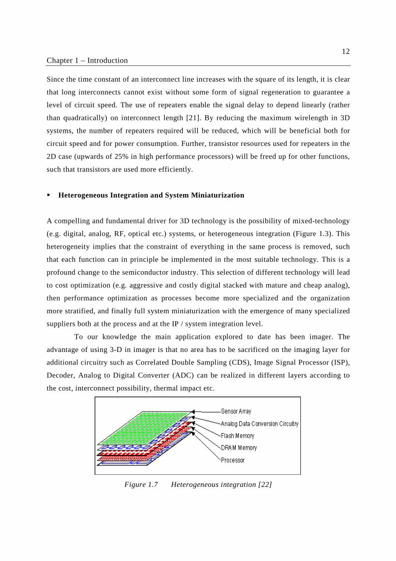
To our knowledge the main application explored to date has been imager. The
advantage of using 3-D in imager is that no area has to be sacrificed on the imaging layer for
additional circuitry such as Correlated Double Sampling (CDS), Image Signal Processor (ISP),
Decoder, Analog to Digital Converter (ADC) can be realized in different layers according to
the cost, interconnect possibility, thermal impact etc.
Figure 1.7 Heterogeneous integration [22]

13
Chapter 1 – Introduction
3D integration is not limited to the above but they also have other advantages such as
parallel processors, new functionalities, new applications etc.
Although 3D technology possesses many potential advantages, it also imposes many
challenges compared to the mature 2D technology. To realize a 3D system, some important
issues must be addressed in the design stage, as explained in the following section.
1.2.3 Issues
As described above, 3D technology has the great potential to overcome issues in planar 2D
technology to pursue the performance levels predicted by Moore's Law and required by
application. . However, the technology also has many obstacles to achieve mainstream
production capability, impacting the feasibility and reliability of systems implemented with
this approach. The main obstacles are described in detail below:
Thinning and mechanical stability
Power consumption[23] creates heat and if it is not dissipated fast enough the temperature of
die increases leading to problems such as increased leakage currents in transistor and reliability
degradation. Moreover the die is thinned before bonding. This adds complication to the heat
dissipation problem: thicker die can spread heat much better than thinner ones along the
horizontal plane.
Apart from heat dissipation problem in the thin die, the 3D stacks will comprise a
number of die of different sizes thinned to a few micrometers, made of materials stacked and
bonded on top of each other so as to retain electrical connections. This system creates lot of
problem in terms of mechanical stability when temperature changes. Different materials have
different thermal expansion coefficients and are affected in different manner by thermal
gradients. This might lead to stack de-bonding leading to electrical failure. Mechanical stress
[24] due to thermal expansion can interfere with the stress carefully engineered in transistor
channel to destroy the on-currents of transistors. Another major source of problem is handling
of the thinned wafers. The thinned wafers are flexible and so extreme care is taken when they
are transferred from one process step to other. So carrier wafers to solve this problem, but still
bonding and de-bonding to carrier wafer may create mechanical issues.
14
Chapter 1 – Introduction • Electromagnetic interference
The increased power consumption per unit area must be considered in a 3D stacked
chip Power Distribution Network (PDN) because total power consumption is proportional to
increased current magnitudes through TSVs and EMI (electromagnetic interference) is
increased by high current switching and high PDN impedances. Although, TSV shows very
small inductance, which is very helpful to 3D IC by giving lower PDN impedance[25].
However, when it combined with the large capacitance of a chip PDN, it can induce high PDN
impedances, which are called as TSV effects or TSV inductance effects and can be an EMI
source in the GHz range as shown in [26]
Thermal issues
One of the main challenges facing 3D integration is heat dissipation. In a conventional 2D
planar approach, a heat sink is attached to the surface of the chip package such that heat flows
straight from the chip to the heat sink. Usually, the heat sink uses the whole area of the 2D
chip, which results in the lowest (best) achievable power density at the heat sink interface. In
this case, there are only two possible approaches: (i) front-cooled, where the heat sink is placed
above the chip and heat flows from the transistor level through the interconnect levels to the
heat sink, and (ii) back-cooled, where the heat sink is placed below the chip and heat flows
from the transistors through the bulk (substrate) to the heat sink. Moving to 3D integration
decreases the chip footprint and both increases power density at the heat sink interface, as well
as multiplying the number of layers that heat has to pass through to reach the heat sink.
Another problem is that upper layers insulate lower layers from the heat sink. Silicon
has a high thermal resistance, so we expect a sharp vertical temperature gradient to develop in
the chip. The temperature rise is discussed in [27]
∆ = 2 + −
2
--(1.4)
where P is the identical chip power dissipation in each layer, n is the total number of active
layers, A is the total 2D chip surface area, R is the identical thermal resistance between layers,
and R1 is the thermal resistance between the top layer and the heat sink. From (1.4)
temperature rise can be expected to rise linearly with power density and the square of number
of active layers. If we assume that R1>>R, then there is an approximately linear relationship

15
Chapter 1 – Introduction between n and ∆. This also suggests that for most 3D-ICs with n≤ 5, R1 will dominate the
rise of temperature in any layer. For example, when moving to a two layered chip, this
relationship indicates that the package thermal resistance has to be halved in order to maintain
the same temperature.
Thermal hotspots [27] are created due to non uniformity in power distribution of
blocks. The local power distribution varies over time and is not uniform due to many factors
such as current flow, transistor size, frequency of operation etc. This condition is exacerbated
by: thermal barrier created by the low thermal conductive interface material used to attach two
layers (e.g. epoxy), longer heat dissipation path from the die to the heat sink is another factor
worsening the local temperature. Thermal hot spots not only increase cooling costs, but also
negatively impact reliability and degrade performance. Hot spots accelerate failure
mechanisms [28] such as electro-migration, stress migration, dielectric breakdown, device
failure and leakage. Leakage is exponentially related to temperature, while the effective carrier
mobility (and consequently operating speed) of devices decreases as temperature increases.
• Design challenges
The addition of a third dimension would require support from more advanced CAD tools due to
the increased complexity [29] of the problem. The 3D system is much larger with many more
dimensions in the design space, tradeoffs and design decisions. Moreover it can be
heterogeneous. The design decisions of such a complex system has to be at the early
architectural exploration.
3D physical design is complex compared to 2D design, each individual design step in
3D has to take the special constraints (e.g Size of the problem, multiple technology database
etc.) of 3D integration into account. Hence, physical design of 3D circuits cannot be simply
viewed as a stack of multiple 2D physical designs. Normally, during physical design, all circuit
components are instantiation with their geometric representations, resulting in a layout
representation of the circuit. In other words, geometric images (shape, size, and metal layer)
of all macros, cells, gates, transistors, etc., are assigned a location using floorplanning. So this
step has to include new, 3D specific characteristics that must be represented in the underlying
data structures. For example, high output power modules need comprehensive consideration of
16
Chapter 1 – Introduction thermal-driven floorplanning [29-31] with vertical dependencies arise in addition to horizontal
ones.
3D placement[32] requires optimizing the placement between multiple active layers.
Since thermal constraints are crucial for 3D designs. Hence, 3D placement must ensure that
thermal considerations are fulfilled. For example, the placement must spread cells such that a
reasonable temperature distribution can be expected. Due to increased package density
additional techniques are required to tackle the heat dissipation issue in 3D designs. Therefore,
vertical metal structures called as thermal vias, play an important role in achieving a thermal
solution. 3D placement problem size is increased (placement of blocks in different tiers along
with optimized placement of thermal vias [30]).
Next major step is 3D interconnect routing[33][34], caused by the multi-tier position
of net terminals that lead to net topologies which span more than one tier. This requires
expensive inter-tier vias to be used in addition to regular signal vias which connect metal
layers within one tier. Furthermore, 3D routing must take additional constraints into account,
such as blockages introduced by thermal and inter-tier vias[30] leading to a more complex heat
management is necessary. Finally, the result of physical design is a set of manufacturing
specifications that must be subsequently verified.
From the above description, it clear that performing a thermal analysis is essential
during the floorplanning at the early stages of design, and this is necessary to avoid very costly
redesign later as the cost of redesign increase with each step of design process. Thermal-aware
floorplanning is performed to determine if modules need to be rearranged in order to control
temperature. The peak temperature and/or the temperature gradient can be reduced by
performing a thermal-aware floorplanning of the chip, consisting of finding an optimum
floorplan that minimizes area, wire length, and maximum temperature. If a hot (power-hungry)
block is placed beside (or, in 3D, above or below) cooler blocks, lateral (and, in 3D, limited
vertical through the insulating layers) spreading of heat takes place. As a result, the
temperature of the hot block is reduced. Floorplanning process can be also used for adding
additional area for thermal vias to reduce temperature. Floorplanning improves the
performance, reliability of the chip. Thermal analysis is also necessary at the end of
verification. This step will not lead to any major redesign if the first floorplanning step is
performed correctly.
17
Chapter 1 – Introduction 1.2.4 3D Imager
Several research groups such as IMEC, CEA-LETI, ST microelectronics, Sony are
working on 3D integration for imagers [35-40]. Massachussets Institute of Technology (MIT)
has reported, 1MP 3D imager [37] with first 2 tiers are a 3D imager, and the supporting 5 tiers
are a multichip silicon stack. The 3D imager is a 2-tier 1024×1024 pixel image sensor array
fabricated with 8µm-pitch, per-pixel 3D vias. The imager is vertically connected to the silicon
stack through agold stud bump array at 500µm pitch. Tier-1 consists of 100% fill factor, deep-
depletion photodiodes, thinned to 50µm. In the year 2010, IMEC has reported its work on area
3D integrated imager with detector layer, analog and digital image processor layer using high
density bumping and area redistributed TSVs. Recently, IMEC has also announced a project on
advanced 3D-Stacked Imager Sensor(3SIS) [41]. CEA-LETI and ST microelectronics has
reported their work on 3D integrated imager in [42].
The next section will discuss about the focus of the research work combining the need
of the imager technology integrated on 3D technology. The focus of the work has been
restricted to few topics which are important from our point of view.
1.3 Research focus
1.3.1 Scalability - Technology
3D integration techniques are proposed as a potential solution to overcome the scaling limit
[43]. The challenge lies in developing a design technique to realize a 3D system. The design
technique has to take care of scaling, simulation capability needed to handle the complex 3D
system and hierarchy to meet all the tradeoffs at early stages of design. When the chip is
represented hierarchically, the design process will find solutions for each block in hierarchical
description. To realize an efficient and reliable hierarchical methodology, it is necessary to
make critical design decisions early on in the design flow, to give a fairly high probability of
achieving first-time design (no reliability or functionality issues) and minimize design cost.
Therefore some information (e.g system netlist) or estimations (e.g. floorplanning) are required
early on in the design process. In the traditional design flow, front-end designers create a
Register Transfer Level (RTL) netlist that is transferred to back-end designers. This netlist
18
Chapter 1 – Introduction mainly covers functionality and interconnectivity, and has low physical information content,
which often results in much iteration between the front-end and the back-end designers. These
iterations have significantly increased for designers with technology scaling. The lack of early
design data during the front end implementation results in initial failure and lead to redesign
which is costly. Technology scaling allows the designer to put an increasing amount of
functionality on a die, but also with greater uncertainty since device variability and overall
system complexity issues are exacerbated.
To overcome the existing problems, models need to be developed at different levels of
abstraction in order to analyze the system and for synthesizing the system. The challenge lies
in formulating a methodology to analyze a system at very early stages that could be optimized
with respect to the intended functionality. Formal abstractions are important to represent an
individual model to fit in the hierarchical design flow. Formulating the problem with proper
specifications (i.e. design constraints and optimization budget) taking into account technology-
related issues confines the problem into acceptable bounds. Constraint propagation between
these models at various abstraction levels is carried out to meet all the requirements can lead to
a successful synthesis. Also the design flow needs to be generic, not only in analyzing the
system but also in integration and testing. The main benefits with this kind of modeling
technique are shorter design time (and consequently time to market), adaptability to new
technology constraints, reusable models.
As explained earlier, 3D design has to undergo rigorous thermal analysis at
floorplanning, placement, routing to have a reliable system. The tool has to be sophisticated to
manage the three dimensional problem. During the modeling and design work the lack of
thermal information at early stages of design was identified. This information is necessary to
analyze the 3D imager system performance. From this understanding deeper focus is given to
understand the impact of thermal aspects on imager performance. The next section will focus
on imager sensor thermal model and 3D integrated thermal model which could create a detailed
analysis into 3D technology.
1.3.2 Simulation scalability– Pixel matrix
In the past few years, the imager industry has evolved to propose imager resolution of 8-12MP
(with an extreme case at 41MP [44]) in mobile phone cameras. This trend seems to be growing
since the consumer is inclined towards higher resolution for improving image
19
Chapter 1 – Introduction quality(averaging) and zooms. From a designer's point of view, the simulation of an entire
pixel matrix at the system level is important in order to analyze the behavior of the pixel
matrix when it interacts with other blocks. Simulating the entire pixel matrix can be useful for
• Early stage exploration of imager
• Analysis of the overall performance
o Identify critical regions based on
Thermal impact
Noise
• Improve the algorithms in ISP based on critical regions
Typical analog and multi-domain simulation environments [45] (Spectre or Pspice or
modeling languages such as VHDL-AMS [46][47], Verilog-A etc.,) are not suitable for the
simulation of high resolution imager matrix structures. It is difficult to make system-level
analysis because of the number of inputs and outputs. For example, since a conventional 3T-
APS has three inputs ("reset" for initialization, "select" for reading and the light intensity
signal itself) as well as two internal nodes (photodiode voltage and amplifier output), and these
are replicated for each pixel in a matrix, a 12MP pixel matrix would require the representation
of 24M input terminals (reset, select), 12M output terminals (readout) and 24M internal nodes
signals. These signals are common for each line, and have to respect precise timings.
In conventional simulation, the light input is often set to be a constant value over the
entire pixel matrix (potentially incremental in a parametric simulation). This kind of simulation
looses the realism in emulating the imager hardware behavior. One challenge is to fix different
values of light for different pixels, where the problem is how to calculate thousands or millions
of design variables. The important point to notice with pixel matrix is that there are millions of
nominally identical modules (pixel), and that brute force simulation does not exploit the
similarity or regularity of the pixel matrix. It is therefore a hugely inefficient approach if we
want to simulate the whole pixel array. Moreover it is anyway impossible to simulate with
current simulator due to machine limitations. It takes several hours to several days to simulate
large matrix. This is the reason typically designers only simulate small matrices to validate the
pixel design, and then just check interconnectivity to validate the matrix. Using the existing
approach it is not possible to 1.look at the actual functionality of the matrix on a whole image,
i.e. carry out a proper validation with realistic application scenarios, and more importantly

20
Chapter 1 – Introduction 2.examine characteristic variations over the pixel matrix and analyse their impact on image
quality. There is therefore a need for
Imager models capable of:
• Simulating large pixel matrix size (scalability) in a reasonable time
• Taking into account heterogeneous input variables (light, temperature,
integration time) for each pixel
Integrated design flow capable of:
• Integrating a complete 3D imager floorplanner with thermal model
• Simulating the integrated model with realistic temperature and light conditions
1.4 Key research contributions
Several research problems related to CMOS image sensors are addressed in this thesis work.
The following are the key contributions:
Demonstration of a methodical analysis of imager design to achieve a high level of
flexibility and modularity. We developed a modeling approach to enable early design
space exploration using a hierarchical approach, and in particular focused on the
development of generic models for imager IC in order to explore early design choices.
Demonstration of a “Thermal-aware imager model” focusing mainly on the thermal
impact on imager performance. Existing electrical simulation tools (Spectre or Pspice)
help in the design of a single pixel, but scale badly to relevant sizes of pixel matrices
since they do not exploit the massive regularity of large pixel matrices and thus lack in
speed and face memory issues. The high-level image sensor models developed in this
work can simulate any size of imager matrix with a specific focus on thermal impact
while overcoming speed and memory issues. Simulation speed-up factors of about
500000x have been achieved using a SystemC model with a relative error of below 4%
(average error of about 500µV for a quanta of 12.9mV) for a 256*256 pixel matrix.
Demonstration of a “3D integrated thermal design flow” integrating floorplanner,
thermal simulation tool and imager thermal model to visualize the impact of various
blocks on the performance of the imager. This flow uses the realistic temperature
distribution of each pixel to produce the output.

21
Chapter 1 – Introduction 1.5 Thesis outline This thesis is organized as follows:
Chapter 2 focuses mainly on the modeling and top-down design approach. The approach is
explained with a supporting methodology, consisting of parameter dependency graphs followed
by segregation into abstraction levels. Some imager blocks such as the pixel matrix and ADC
are chosen to illustrate the methodology. Another methodology based on Pareto fronts is also
explained to illustrate the importance of performance tradeoffs.
Chapter 3 focuses mainly on the thermal aspects when moving into 3D technology. Initially,
image sensor thermal modeling and requirements are discussed in detail, followed by the
description of a methodology to realize the thermal model. The validation of the model is
explained by supporting results, and is followed by the implementation of the imager thermal
model in SystemC to simulate any pixel matrix size. Finally, the SystemC model is concluded
by a validation phase.
Chapter 4 focuses on further development of the imager thermal model discussed in earlier
chapters through the establishment of a 3D integrated thermal design flow. This chapter
explains in details the need for an integrated thermal design flow including floorplanning,
thermal simulations of the imager thermal model with a realistic thermal map and input light
generated from an image. Finally the chapter is concluded with results with several test cases.
Chapter 5 This chapter concludes the thesis with final outcome and future perspectives.
Supporting code, and model and tool parameters are attached in the appendices of the thesis.
22
Chapter 1 – Introduction Bibliography
[1] El Gamal, H.Eltoukh,. “CMOS Image sensors”. IEEE Circuits and Devices magazine. 21(3), 2005, 6-20.
[2] S.H.Lim, “Video processing applications of high speed CMOS image sensors”, Stanford university, 2003, Thesis.
[3] Micron corporation,. CMOS's advantages (technical notes): http://www.micron.com/imaging/Technology/CMOS_Advantages/index.html.
[4] E.R Fossum, “CMOS image sensors:electronic camera on a chip”, Washington DC, USA : Proceedings of international electron devices, Dec 1995. p.no:17-25.
[5] H.S.Wong, “Technology and device scaling considerations for CMOS Imagers”, IEEE Transactions on Electron devices, Dec 1996, Vol. 43. 2131-2141.
[6] Kleinfelder, “A 10,000 frames per second CMOS digital pixel sensor”, IEEE solid state circuits, 2001, Vol. 36. 2049-2059.
[7] K.Tajima et al, “Development of a high-resolution, high-speed vision system using CMOS image sensor technology enhanced by intelligent pixel selection technique”, Whitepaper, Photron Inc.
[8] P.Fry, P.Noble, R.Rycroft, “ Fixed pattern noise in photomatrices”, IEEE J. Solid state circuits, 1970, Vol. SC-5. 250-254.
[9] E.R.Fossum, “CMOS image sensors”, IEEE transactions on electron devices, 1997, Vol. 44. 1689-1698.
[10] X.Wang, “Noise in submicron CMOS image sensors”, Delft university of technology, 2008, Thesis.
[11] J.S.Lee, “Photoresponse of CMOS image sensors”, University of waterloo, 2003.
[12] Suat Utku Ay, “Large format CMOS image sensors performance and design”,VDM Verlag Dr.Muller & co, Published 2008, ISBN: 978-3-8364-7052-0
23
Chapter 1 – Introduction [13] U. Kang et al., “8Gb 3D DDR3 DRAM using through-silicon-via
technology,” in ISSCC Dig. Tech. Papers, 2009, pp. 130–131
[14] K. Osada et al., “3D system integration of processor and multi- stacked SRAMs by using inductive coupling links,” in Symp. VLSI Circuits, Dig. Tech. Papers, 2009, pp.256–257.
[15] J.D.Meindl, “Beyond Moore's law: the interconnect era”, Computing in science and engineering, Jan 2003, Vol. 5. p20-24.
[16] ASE. http://www.asejp.aseglobal.com/.
[17] Vasilis.F.Pavlidis, Eby G.Friedman, “Three dimensional integrated circuit design”, Elsevier, 2009.
[18] Craig Keast et al, “ 3D integration for integrated circuits and advanced focal planes”, Fermilab colloquim, Feb 2007.
[19] A. Papanikolaou et al. (eds.), Three Dimensional System Integration: IC Stacking 13 Process and Design, DOI 10.1007/978-1-4419-0962-6_2, Springer Science+Business Media, LLC 2011
[20] International Technology Roadmap for Semiconductors (ITRS), 2011 http://www.itrs.net/Links/2011ITRS/2011Chapters/2011Interconnect.pdf
[21] T. Sakurai, “Closed-form expressions for interconnect delay, coupling,and crosstalk in VLSIs,” IEEE Trans. Electron Devices, vol. 40, pp.118–124, Jan. 1993
[22] http://www.tezzaron.com/technology/FaStack.htm.
[23] Yuan Xie et al, “Three dimensional integrated circuit design, EDA, design and microarchitecture”, Springer, Dec 2009
[24] Antonis Papanikolaou et al, “Three dimensional system integration : IC stacking process and design”, Book, Springer, Dec 2010
[25] J. S. Pak, C. Ryu, and J. Kim, "Electrical characterization of through silicon via (TSV) depending on structural and material parameters based on 3D full wave simulation," in Proceedings of the 9th International Symposium on Electronic Materials and Packaging, Daejeon, Korea, Nov. 2007.
24
Chapter 1 – Introduction [26] J. S. Pak, et al, "Slow wave and dielectric quasi-TEM modes of metal-
insulator-semiconductor structure through silicon via in signal propagation and power delivery in 3D chip package," Proc. of the 60th Electronic Components and Technology Conference 2010 (ECTC 2010), Las Vegas, USA, Jun. 2010.
[27] K.Banerjee, S.J.Souri et al ,“3D ICS: A novel chip design for improving deep-submicrometer interconnect performance and systems-on-chip integration”, Proceedings of the IEEE, May 2001. 89(5): 602-633.
[28] JEDEC, JEP122C, “Failure mechanisms and models for semiconductor devices”, http://www.jedec.org.
[29] Yuan Xie, Gabriel Loh, Bryan Black, and Kerry Bernstein, "Design Space Exploration for 3D Architecture." ACM Journal of Emerging Technologies for Computer Systems, Vol. 2. No. 2, pp.65-103, April 2006
[30] B.Goplen, S.S.Saptnekar, “Thermal via placement in 3D ICs”, ISPD, 2005. 167-174.
[31] P. Zhou et al. 3D-STAF: scalable temperature and leakage aware floorplanning for three-dimensional integrated circuits. In ICCAD, pages 590–597, 2007
[32] N. Viswanathan and C. C.-N. Chu. FastPlace:Efficient analytical placement using cell shifting, iterative local refinement,and a hybrid net model. IEEE T. Comput. Aid. D., 24(5):722–733, 2005.
[33] T. Zhang, Y. Zhan, and S. S. Sapatnekar, “Temperature-aware routing in 3D ICs”. In ASPDAC, pages 309–314, 2006.
[34] J. Cong and Y. Zhang. Thermal-driven multilevel routing for 3D ICs. In ASPDAC, pages 121–126,2005.
[35] B. Aull, et. al., “Laser Radar Imager Based on 3D Integration of Geiger-Mode Avalanche Photodiodes with Two SOI Timing Circuit layers”, ISSCC 2006, pp 26-27.
[36] D. Temple, et. al.,“3-D Integration Technology Platform for High Performance Detector Arrays”, public release from RTI International and DRS Technologies.
25
Chapter 1 – Introduction [37] V. Suntharalingam, et al., “A 4-side Tileable Back Illuminated 3D-integrated
Mpixel CMOS Image Sensor.” Solid-State Circuits Conference -Digest of Technical Papers, 2009. ISSCC 2009.
[38] V. Suntharalingam et al., “Megapixel cmos image sensor fabricated in three-dimensional integrated circuit technology,” Digest of Technical Papers, IEEE International Solid-State Circuits Conference, pp. 356–357 Vol. 1, Feb. 2005
[39] Orit Soraka, Dileepan Joseph, “Design and Fabrication of Vertically-Integrated CMOS Image Sensors”, Sensors 2011, vol. 11, pp. 4512-4538;
[40] M. Motoyoshi, H. Nakamura, M. Bonkohara, and M. Koyanagi, “Current and future 3D-LSI technology for image sensor devices,” Mater. Res. Soc. Symp., Proc., vol. 1112, E01-03.
[41] Advanced 3D-Stacked Image Sensor (3SIS). https://projects.imec.be/3sis/
[42] Jaffard and Yvon Cazaux, “Image sensors with 3D heterogeneous integration"http://www.cnfm.fr/VersionFrancaise/actualites/GIP_CO09_presentations%20pour%20WEB-CNFM/Atelier3_conception_3D/Jaffard.pdf
[43] W.R.Davis, J.Wilson et al,“Demistifiying 3D ICs: The Pros and Cons of Going Vertical”, IEEE design test of computer, Dec 2005, Vol. 22. pp 498-510.
[44] http://www.nokia.com/us-en/products/phone/808/specifications/
[45] D.Navarro, Z.Feng, V.Viswanathan, I.O'Connor, “Image toolbox for CMOS Image sensors simulation in Cadence ADE”,: Demset, Dec 2011, Florida, USA.
[46] D.Navarro, D.Ramat, F.Mieyeville, I.O'Connor, F.Gaffiot, L.Carrel , “VHDL & VHDL-AMS modeling and simulation of a CMOS imager IP”, Forum on specification & design languages, Sep 2005, Lausanne, Switzerland.
[47] F.Dadouche et al,“Modelling of pixel sensors for image systems with VHDL-AMS”, in: International journal of electronics, 95:3(211-225),2008
[48] S.Feruglio et al.,“Exact noise analysis of a CMOS BDJ APS”, ISCAS (3) 2005: 2337-2340
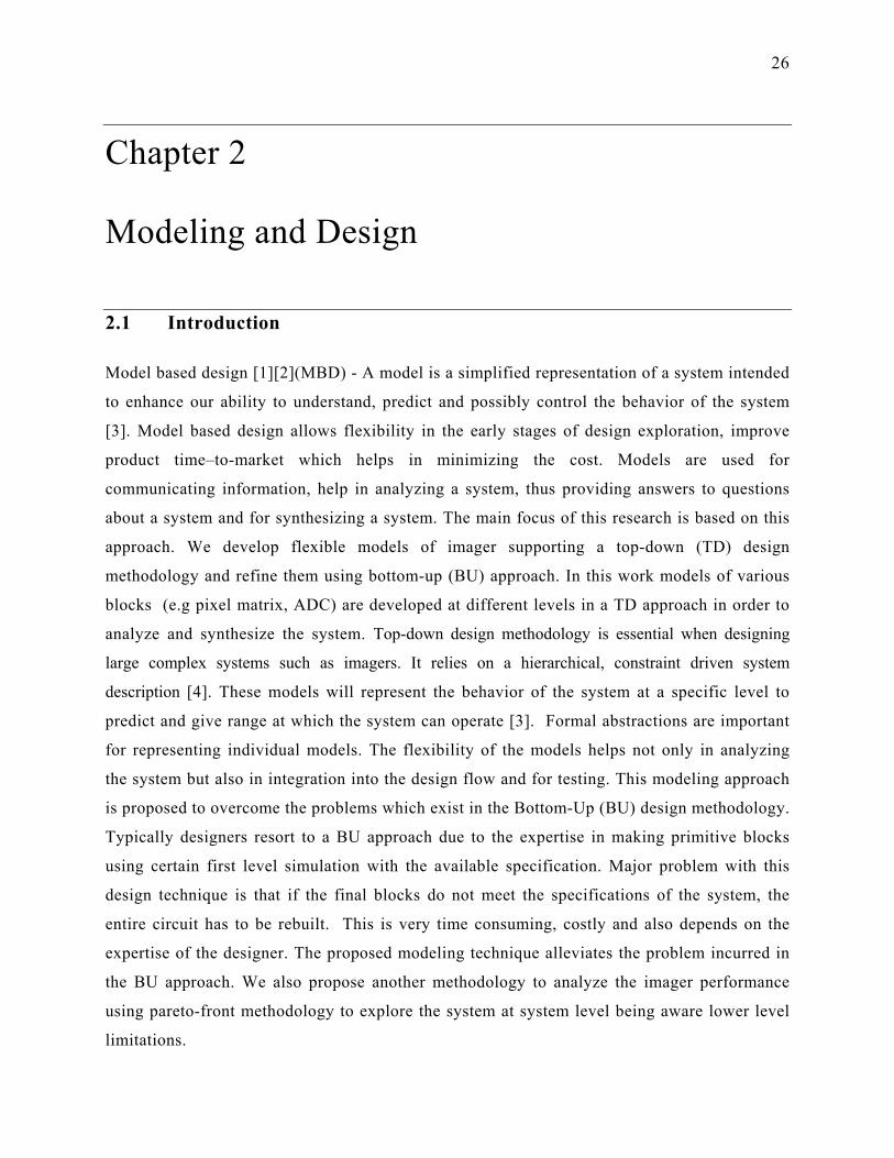
26
Chapter 2 Modeling and Design
2.1 Introduction
Model based design [1][2](MBD) - A model is a simplified representation of a system intended
to enhance our ability to understand, predict and possibly control the behavior of the system
[3]. Model based design allows flexibility in the early stages of design exploration, improve
product time–to-market which helps in minimizing the cost. Models are used for
communicating information, help in analyzing a system, thus providing answers to questions
about a system and for synthesizing a system. The main focus of this research is based on this
approach. We develop flexible models of imager supporting a top-down (TD) design
methodology and refine them using bottom-up (BU) approach. In this work models of various
blocks (e.g pixel matrix, ADC) are developed at different levels in a TD approach in order to
analyze and synthesize the system. Top-down design methodology is essential when designing
large complex systems such as imagers. It relies on a hierarchical, constraint driven system
description [4]. These models will represent the behavior of the system at a specific level to
predict and give range at which the system can operate [3]. Formal abstractions are important
for representing individual models. The flexibility of the models helps not only in analyzing
the system but also in integration into the design flow and for testing. This modeling approach
is proposed to overcome the problems which exist in the Bottom-Up (BU) design methodology.
Typically designers resort to a BU approach due to the expertise in making primitive blocks
using certain first level simulation with the available specification. Major problem with this
design technique is that if the final blocks do not meet the specifications of the system, the
entire circuit has to be rebuilt. This is very time consuming, costly and also depends on the
expertise of the designer. The proposed modeling technique alleviates the problem incurred in
the BU approach. We also propose another methodology to analyze the imager performance
using pareto-front methodology to explore the system at system level being aware lower level
limitations.
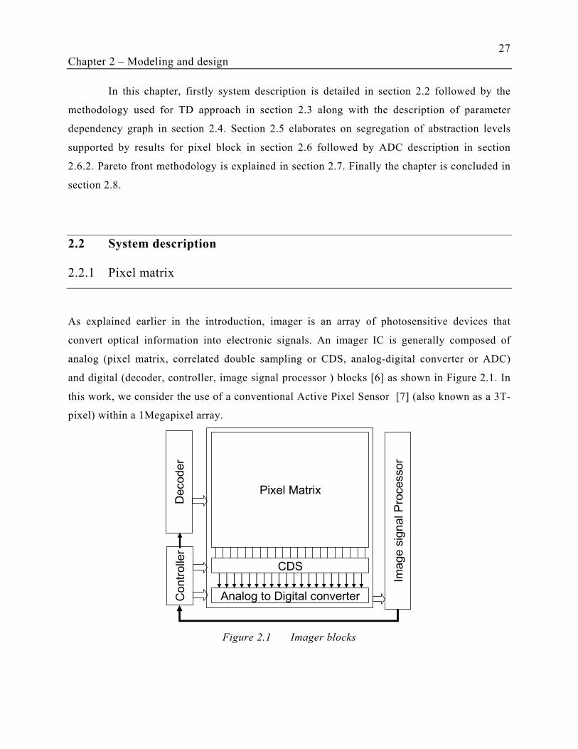
27
Chapter 2 – Modeling and design
In this chapter, firstly system description is detailed in section 2.2 followed by the
methodology used for TD approach in section 2.3 along with the description of parameter
dependency graph in section 2.4. Section 2.5 elaborates on segregation of abstraction levels
supported by results for pixel block in section 2.6 followed by ADC description in section
2.6.2. Pareto front methodology is explained in section 2.7. Finally the chapter is concluded in
section 2.8.
2.2 System description
2.2.1 Pixel matrix
As explained earlier in the introduction, imager is an array of photosensitive devices that
convert optical information into electronic signals. An imager IC is generally composed of
analog (pixel matrix, correlated double sampling or CDS, analog-digital converter or ADC)
and digital (decoder, controller, image signal processor ) blocks [6] as shown in Figure 2.1. In
this work, we consider the use of a conventional Active Pixel Sensor [7] (also known as a 3T-
pixel) within a 1Megapixel array.
Pixel Matrix
CDS
Analog to Digital converterContr
olle
r
Image s
ign
al P
rocessor
Decoder
Figure 2.1 Imager blocks
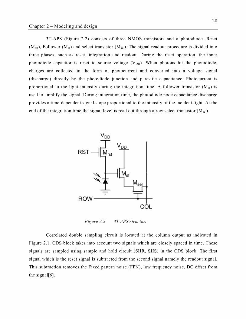
28
Chapter 2 – Modeling and design
3T-APS (Figure 2.2) consists of three NMOS transistors and a photodiode. Reset
(Mrst), Follower (Msf) and select transistor (Msel). The signal readout procedure is divided into
three phases, such as reset, integration and readout. During the reset operation, the inner
photodiode capacitor is reset to source voltage (VDD). When photons hit the photodiode,
charges are collected in the form of photocurrent and converted into a voltage signal
(discharge) directly by the photodiode junction and parasitic capacitance. Photocurrent is
proportional to the light intensity during the integration time. A follower transistor (Msf) is
used to amplify the signal. During integration time, the photodiode node capacitance discharge
provides a time-dependent signal slope proportional to the intensity of the incident light. At the
end of the integration time the signal level is read out through a row select transistor (Msel).
Correlated double sampling circuit is located at the column output as indicated in
Figure 2.1. CDS block takes into account two signals which are closely spaced in time. These
signals are sampled using sample and hold circuit (SHR, SHS) in the CDS block. The first
signal which is the reset signal is subtracted from the second signal namely the readout signal.
This subtraction removes the Fixed pattern noise (FPN), low frequency noise, DC offset from
the signal[6].
Figure 2.2 3T APS structure
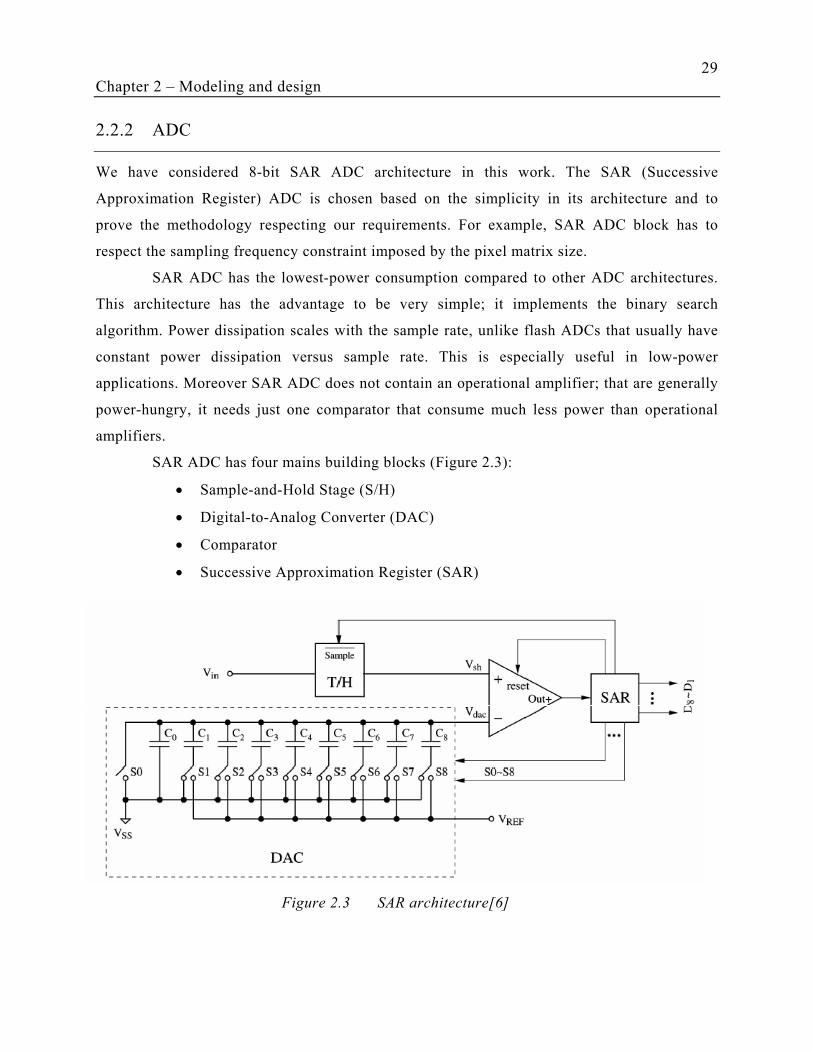
29
Chapter 2 – Modeling and design
2.2.2 ADC
We have considered 8-bit SAR ADC architecture in this work. The SAR (Successive
Approximation Register) ADC is chosen based on the simplicity in its architecture and to
prove the methodology respecting our requirements. For example, SAR ADC block has to
respect the sampling frequency constraint imposed by the pixel matrix size.
SAR ADC has the lowest-power consumption compared to other ADC architectures.
This architecture has the advantage to be very simple; it implements the binary search
algorithm. Power dissipation scales with the sample rate, unlike flash ADCs that usually have
constant power dissipation versus sample rate. This is especially useful in low-power
applications. Moreover SAR ADC does not contain an operational amplifier; that are generally
power-hungry, it needs just one comparator that consume much less power than operational
amplifiers.
SAR ADC has four mains building blocks (Figure 2.3):
• Sample-and-Hold Stage (S/H)
• Digital-to-Analog Converter (DAC)
• Comparator
• Successive Approximation Register (SAR)
Figure 2.3 SAR architecture[6]
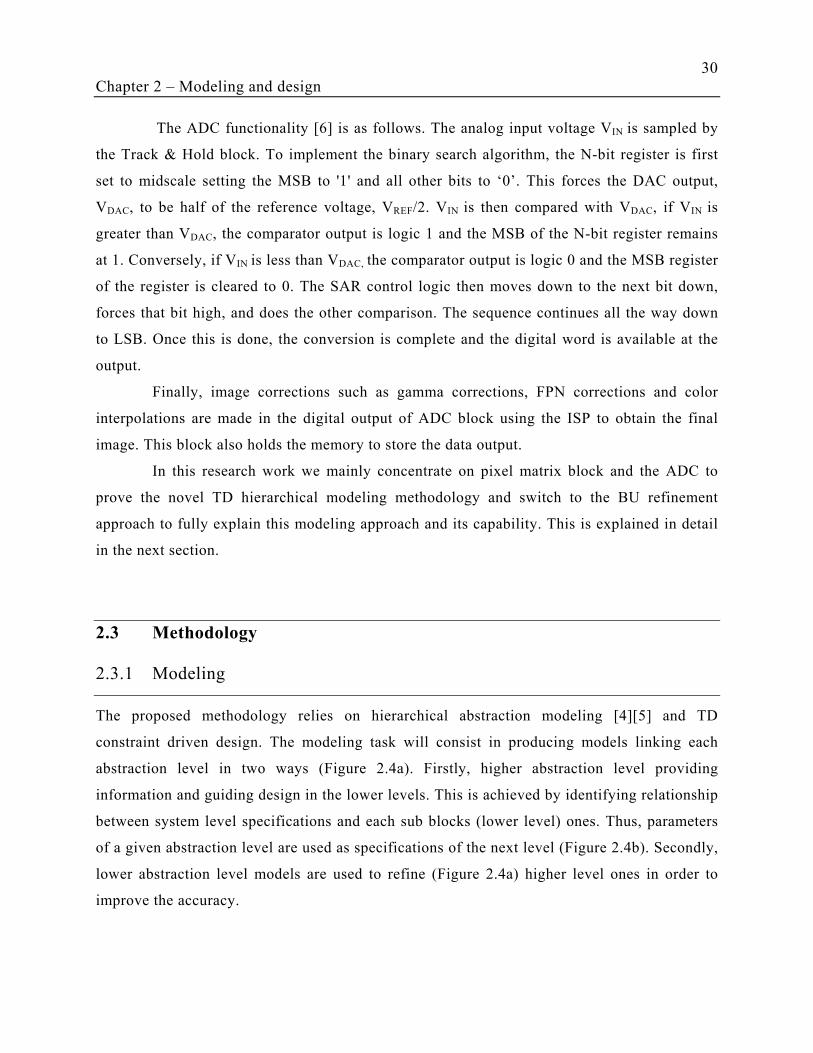
30
Chapter 2 – Modeling and design
The ADC functionality [6] is as follows. The analog input voltage VIN is sampled by
the Track & Hold block. To implement the binary search algorithm, the N-bit register is first
set to midscale setting the MSB to '1' and all other bits to ‘0’. This forces the DAC output,
VDAC, to be half of the reference voltage, VREF/2. VIN is then compared with VDAC, if VIN is
greater than VDAC, the comparator output is logic 1 and the MSB of the N-bit register remains
at 1. Conversely, if VIN is less than VDAC, the comparator output is logic 0 and the MSB register
of the register is cleared to 0. The SAR control logic then moves down to the next bit down,
forces that bit high, and does the other comparison. The sequence continues all the way down
to LSB. Once this is done, the conversion is complete and the digital word is available at the
output.
Finally, image corrections such as gamma corrections, FPN corrections and color
interpolations are made in the digital output of ADC block using the ISP to obtain the final
image. This block also holds the memory to store the data output.
In this research work we mainly concentrate on pixel matrix block and the ADC to
prove the novel TD hierarchical modeling methodology and switch to the BU refinement
approach to fully explain this modeling approach and its capability. This is explained in detail
in the next section.
2.3 Methodology
2.3.1 Modeling
The proposed methodology relies on hierarchical abstraction modeling [4][5] and TD
constraint driven design. The modeling task will consist in producing models linking each
abstraction level in two ways (Figure 2.4a). Firstly, higher abstraction level providing
information and guiding design in the lower levels. This is achieved by identifying relationship
between system level specifications and each sub blocks (lower level) ones. Thus, parameters
of a given abstraction level are used as specifications of the next level (Figure 2.4b). Secondly,
lower abstraction level models are used to refine (Figure 2.4a) higher level ones in order to
improve the accuracy.
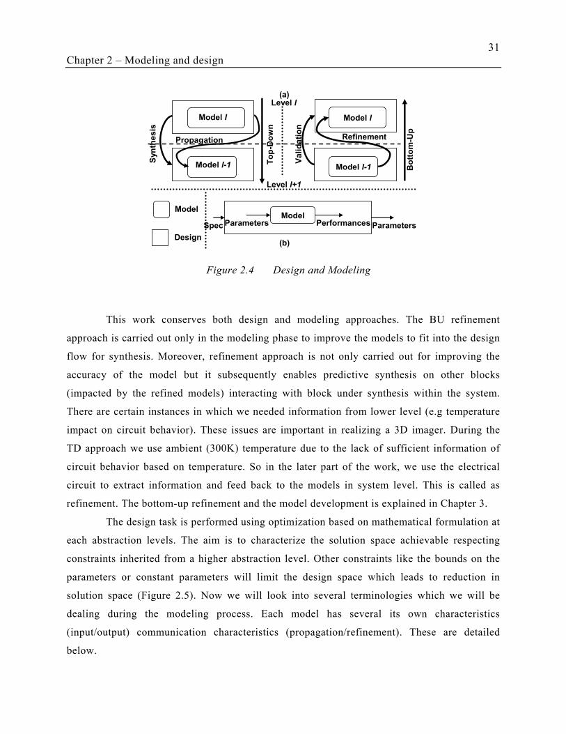
31
Chapter 2 – Modeling and design
Model l-1
Model l
Model l-1
Refinement
Bo
tto
m-U
p
Model
Design
To
p-D
ow
n
Propagation
Syn
the
sis
PerformancesModel
ParametersSpec Parameters
Model l
Level l
Level l+1
Va
lid
ati
on
(a)
(b)
This work conserves both design and modeling approaches. The BU refinement
approach is carried out only in the modeling phase to improve the models to fit into the design
flow for synthesis. Moreover, refinement approach is not only carried out for improving the
accuracy of the model but it subsequently enables predictive synthesis on other blocks
(impacted by the refined models) interacting with block under synthesis within the system.
There are certain instances in which we needed information from lower level (e.g temperature
impact on circuit behavior). These issues are important in realizing a 3D imager. During the
TD approach we use ambient (300K) temperature due to the lack of sufficient information of
circuit behavior based on temperature. So in the later part of the work, we use the electrical
circuit to extract information and feed back to the models in system level. This is called as
refinement. The bottom-up refinement and the model development is explained in Chapter 3.
The design task is performed using optimization based on mathematical formulation at
each abstraction levels. The aim is to characterize the solution space achievable respecting
constraints inherited from a higher abstraction level. Other constraints like the bounds on the
parameters or constant parameters will limit the design space which leads to reduction in
solution space (Figure 2.5). Now we will look into several terminologies which we will be
dealing during the modeling process. Each model has several its own characteristics
(input/output) communication characteristics (propagation/refinement). These are detailed
below.
Figure 2.4 Design and Modeling
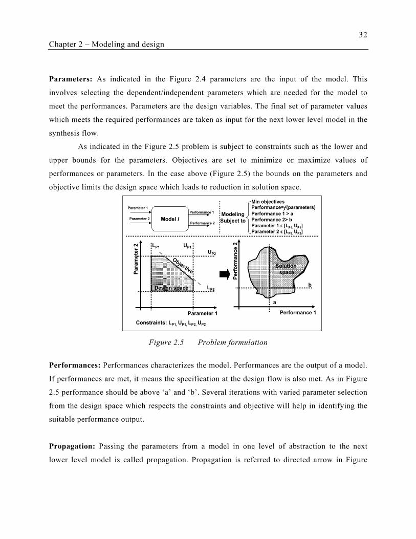
32
Chapter 2 – Modeling and design
Parameters: As indicated in the Figure 2.4 parameters are the input of the model. This
involves selecting the dependent/independent parameters which are needed for the model to
meet the performances. Parameters are the design variables. The final set of parameter values
which meets the required performances are taken as input for the next lower level model in the
synthesis flow.
As indicated in the Figure 2.5 problem is subject to constraints such as the lower and
upper bounds for the parameters. Objectives are set to minimize or maximize values of
performances or parameters. In the case above (Figure 2.5) the bounds on the parameters and
objective limits the design space which leads to reduction in solution space.
Model l
Parameter 1
Parameter 2
Performance 1
Performance 2
Design space
Parameter 1
Pa
ram
ete
r 2
UP2
LP2
UP1LP1
Performance 1
Pe
rfo
rma
nc
e 2
Solution
space
Objective
Constraints: LP1, UP1, LP2, UP2
Modeling
Subject to
Min objectivesPerformance=f f f f (parameters)
Performance 1 > a
Performance 2> b
Parameter 1 ϵ [LP1, UP1]
Parameter 2 ϵ [LP2, UP2]
a
b
Figure 2.5 Problem formulation
Performances: Performances characterizes the model. Performances are the output of a model.
If performances are met, it means the specification at the design flow is also met. As in Figure
2.5 performance should be above ‘a’ and ‘b’. Several iterations with varied parameter selection
from the design space which respects the constraints and objective will help in identifying the
suitable performance output.
Propagation: Passing the parameters from a model in one level of abstraction to the next
lower level model is called propagation. Propagation is referred to directed arrow in Figure
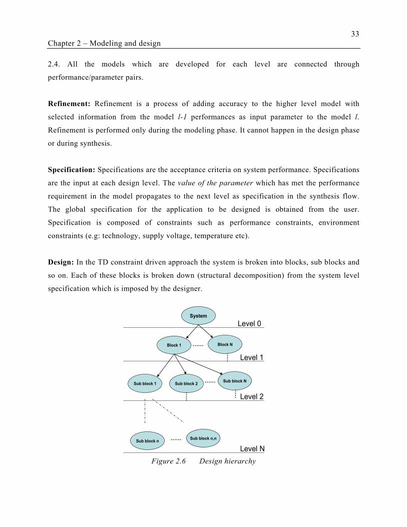
33
Chapter 2 – Modeling and design
2.4. All the models which are developed for each level are connected through
performance/parameter pairs.
Refinement: Refinement is a process of adding accuracy to the higher level model with
selected information from the model l-1 performances as input parameter to the model l.
Refinement is performed only during the modeling phase. It cannot happen in the design phase
or during synthesis.
Specification: Specifications are the acceptance criteria on system performance. Specifications
are the input at each design level. The value of the parameter which has met the performance
requirement in the model propagates to the next level as specification in the synthesis flow.
The global specification for the application to be designed is obtained from the user.
Specification is composed of constraints such as performance constraints, environment
constraints (e.g: technology, supply voltage, temperature etc).
Design: In the TD constraint driven approach the system is broken into blocks, sub blocks and
so on. Each of these blocks is broken down (structural decomposition) from the system level
specification which is imposed by the designer.
Figure 2.6 Design hierarchy
System
Block 1 Block N
Sub block 1 Sub block 2Sub block N
Sub block nSub block n,n
Level 0
Level 1
Level 2
Level N

34
Chapter 2 – Modeling and design
In the BU approach designers perform certain first level simulation with specification
relevant to individual blocks and synthesize the blocks. Each of these blocks are connected
together to make the system. Major problem with this design technique is that, if the final
blocks do not meet the system specifications, the entire circuit has to be rebuilt. To overcome
the long design time in BU approach and to avoid the rebuilding of the entire system if the
system specification is not met, we choose the TD constraint driven approach evaluate at
system level and build our system.
A Design can be broken into different abstraction levels. Here Level 0 represents the
system level and Level N represents the layout level. These levels increases in computational
complexity when we go down (level 0level N) and decomposes each component into sub
components (Figure 2.6). Lowest level component will be the primitive components (transistor,
diode etc.). In the BU, we design from primitive components to high level block (level
Nlevel 0). The flow (directed arrows) is followed until all the sub blocks in the design space
are synthesized.Now that we know what is a model, their input/outputs. To communicate
between each model we need a methodology. This is explained in the next section.
2.4 Parameter dependency graph
2.4.1 Formulation
We know the design variables, input and output of a model. But there is a lack of methodology
to identify interdependencies between design variable and communicating between different
variables. So we propose the parameter dependency graph to overcome this problem.
Dependency graph is a directed graph representing inter-dependencies of several parameters.
Order of dependency identified in such graphs support in characterizing each of the models at
different level. This characterization also supports the propagation from one level to the other.
Nevertheless, dependencies are also possible between parameters in the same level which leads
to encapsulation of dependent parameters in an abstraction level.
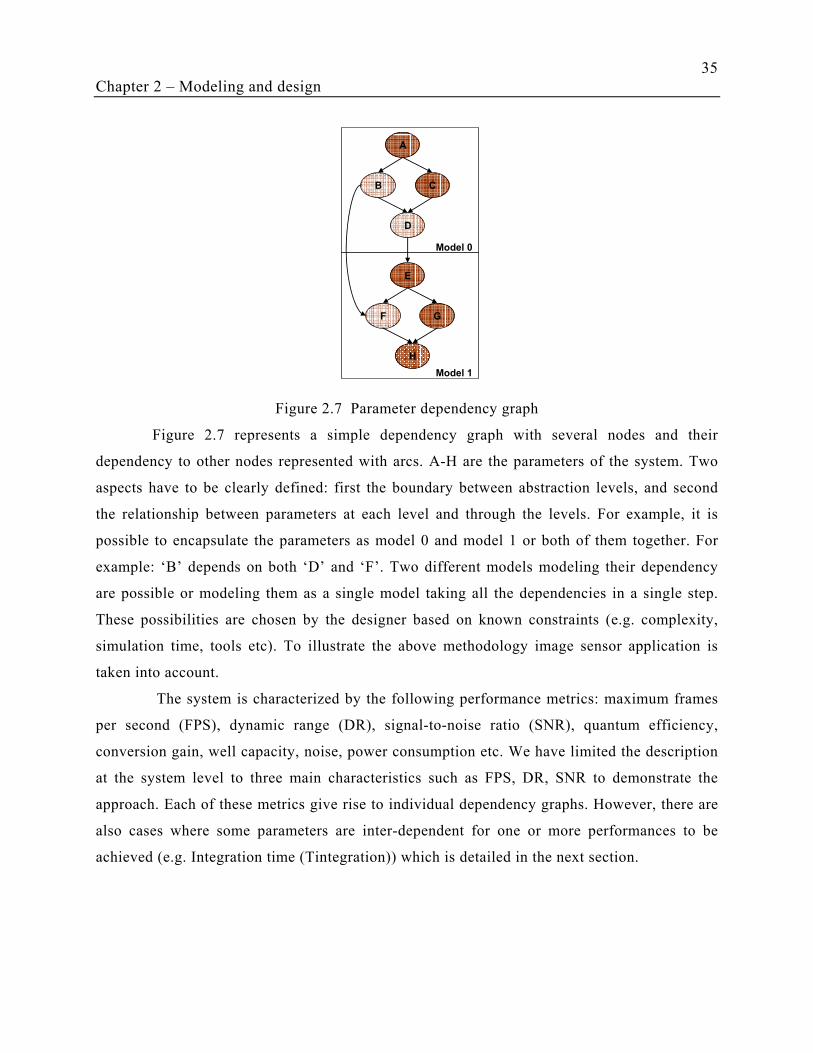
35
Chapter 2 – Modeling and design
A
B C
D
E
F G
H
Model 0
Model 1
Figure 2.7 Parameter dependency graph
Figure 2.7 represents a simple dependency graph with several nodes and their
dependency to other nodes represented with arcs. A-H are the parameters of the system. Two
aspects have to be clearly defined: first the boundary between abstraction levels, and second
the relationship between parameters at each level and through the levels. For example, it is
possible to encapsulate the parameters as model 0 and model 1 or both of them together. For
example: ‘B’ depends on both ‘D’ and ‘F’. Two different models modeling their dependency
are possible or modeling them as a single model taking all the dependencies in a single step.
These possibilities are chosen by the designer based on known constraints (e.g. complexity,
simulation time, tools etc). To illustrate the above methodology image sensor application is
taken into account.
The system is characterized by the following performance metrics: maximum frames
per second (FPS), dynamic range (DR), signal-to-noise ratio (SNR), quantum efficiency,
conversion gain, well capacity, noise, power consumption etc. We have limited the description
at the system level to three main characteristics such as FPS, DR, SNR to demonstrate the
approach. Each of these metrics give rise to individual dependency graphs. However, there are
also cases where some parameters are inter-dependent for one or more performances to be
achieved (e.g. Integration time (Tintegration)) which is detailed in the next section.
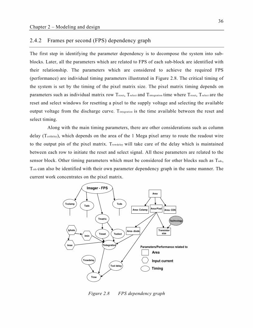
36
Chapter 2 – Modeling and design
2.4.2 Frames per second (FPS) dependency graph
The first step in identifying the parameter dependency is to decompose the system into sub-
blocks. Later, all the parameters which are related to FPS of each sub-block are identified with
their relationship. The parameters which are considered to achieve the required FPS
(performance) are individual timing parameters illustrated in Figure 2.8. The critical timing of
the system is set by the timing of the pixel matrix size. The pixel matrix timing depends on
parameters such as individual matrix row Treset, Tselect and Tintegration time where Treset, Tselect are the
reset and select windows for resetting a pixel to the supply voltage and selecting the available
output voltage from the discharge curve. Tintegration is the time available between the reset and
select timing.
Along with the main timing parameters, there are other considerations such as column
delay (Tcoldelay), which depends on the area of the 1 Mega pixel array to route the readout wire
to the output pin of the pixel matrix. Trowdelay will take care of the delay which is maintained
between each row to initiate the reset and select signal. All these parameters are related to the
sensor block. Other timing parameters which must be considered for other blocks such as Tadc,
Tcds can also be identified with their own parameter dependency graph in the same manner. The
current work concentrates on the pixel matrix.
Treset Tselect
Trow
Tcol delay
Trowdelay
Tmatrix
TadcTcdsTcolamp
Imager - FPS
Tintegration
Technology
Area
Input current
Timing
Parameters/Performance related toImax
Imin
Iphoto
Area
Area- CDSArea-PixelArea- Colamp
Area- diode Transistor
size
Figure 2.8 FPS dependency graph
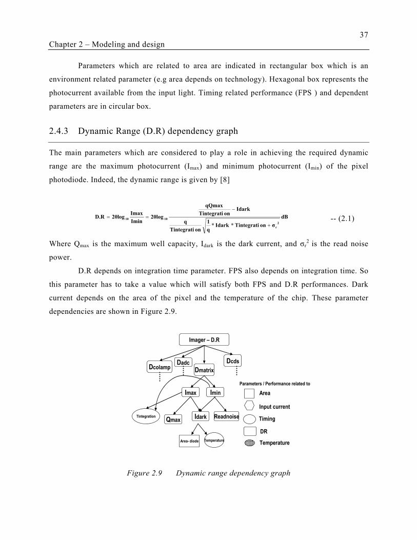
37
Chapter 2 – Modeling and design
Parameters which are related to area are indicated in rectangular box which is an
environment related parameter (e.g area depends on technology). Hexagonal box represents the
photocurrent available from the input light. Timing related performance (FPS ) and dependent
parameters are in circular box.
2.4.3 Dynamic Range (D.R) dependency graph
The main parameters which are considered to play a role in achieving the required dynamic
range are the maximum photocurrent (Imax) and minimum photocurrent (Imin) of the pixel
photodiode. Indeed, the dynamic range is given by [8]
dB
σonTintegrati*Idark*q
1
onTintegrati
q
IdarkonTintegrati
qQmax
20logImin
Imax20logD.R
2
r
1010
+
−
==
-- (2.1)
Where Qmax is the maximum well capacity, Idark is the dark current, and σr2 is the read noise
power.
D.R depends on integration time parameter. FPS also depends on integration time. So
this parameter has to take a value which will satisfy both FPS and D.R performances. Dark
current depends on the area of the pixel and the temperature of the chip. These parameter
dependencies are shown in Figure 2.9.
Tintegration
Temperature
Parameters / Performance related to
DR
Area
Input current
Timing
TemperatureArea- diode
Imager – D.R
DcolampDadc
Dmatrix
Dcds
Imax Imin
IdarkQmaxReadnoise
Figure 2.9 Dynamic range dependency graph
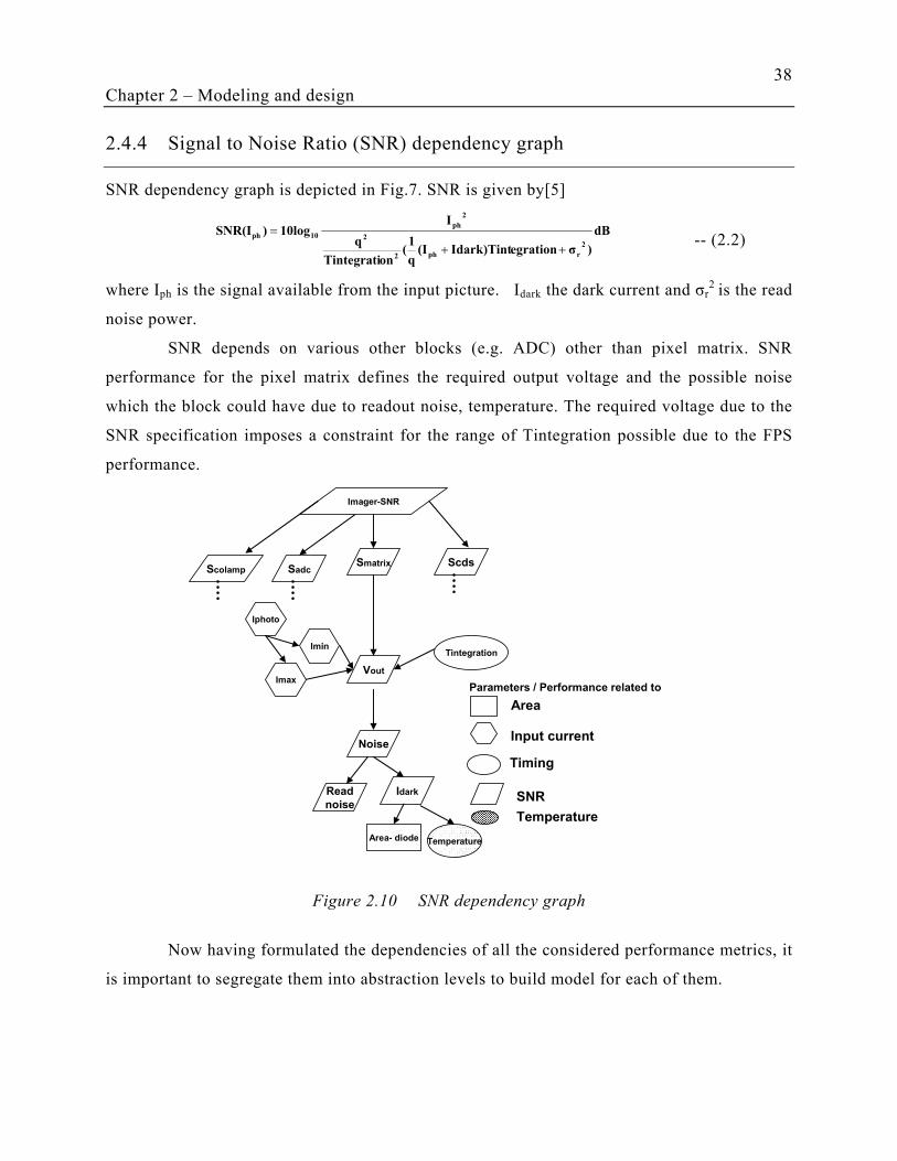
38
Chapter 2 – Modeling and design
2.4.4 Signal to Noise Ratio (SNR) dependency graph
SNR dependency graph is depicted in Fig.7. SNR is given by[5]
dB
)σegrationIdark)Tint(Iq
1(
onTintegrati
q
I10log)SNR(I
2
rph2
2
2
ph
10ph
++
=
-- (2.2)
where Iph is the signal available from the input picture. Idark the dark current and σr2 is the read
noise power.
SNR depends on various other blocks (e.g. ADC) other than pixel matrix. SNR
performance for the pixel matrix defines the required output voltage and the possible noise
which the block could have due to readout noise, temperature. The required voltage due to the
SNR specification imposes a constraint for the range of Tintegration possible due to the FPS
performance.
Figure 2.10 SNR dependency graph
Now having formulated the dependencies of all the considered performance metrics, it
is important to segregate them into abstraction levels to build model for each of them.
Tintegration
Temperature
Parameters / Performance related to
SNR
Imager-SNR
Scolamp SadcSmatrix Scds
Vout
Noise
Read
noise
Idark
Imax
Imin
Iphoto
Area- diode
Area
Input current
Timing
Temperature
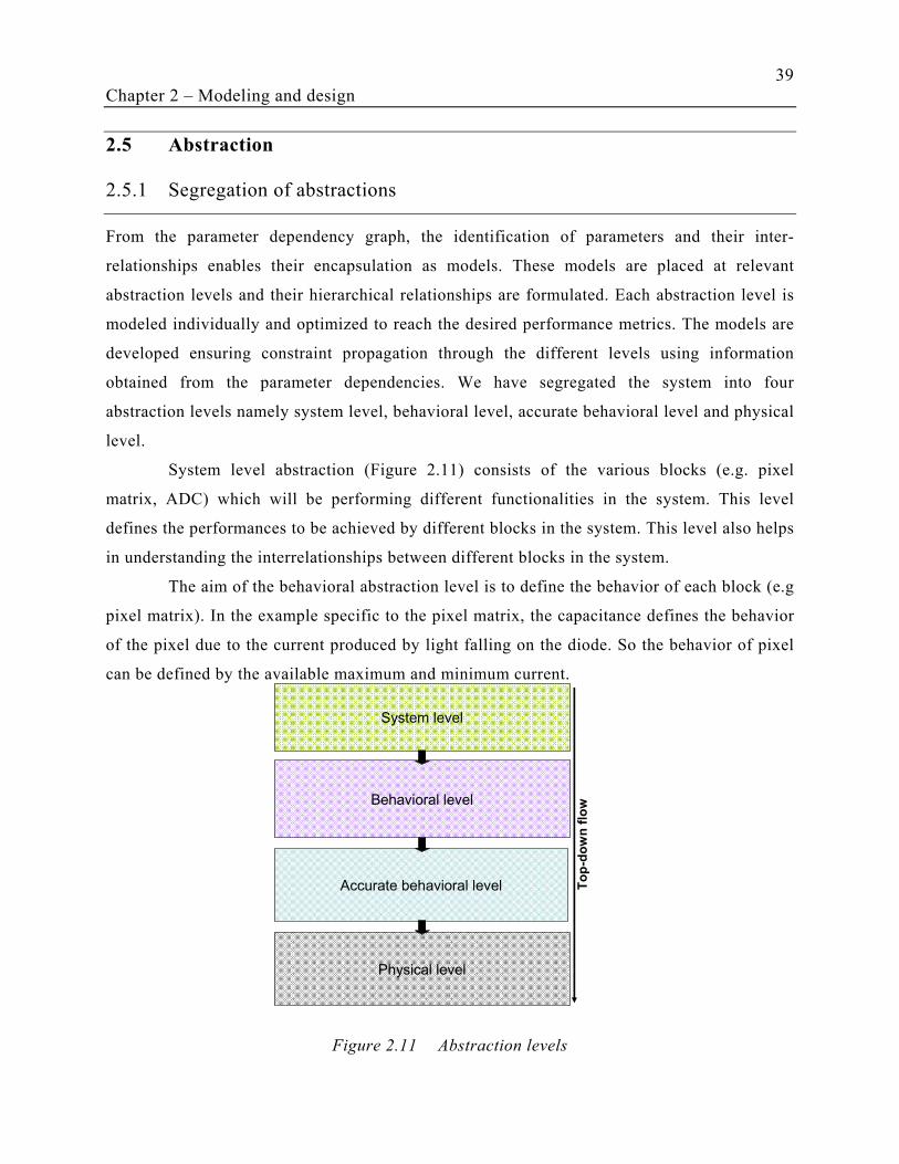
39
Chapter 2 – Modeling and design
2.5 Abstraction
2.5.1 Segregation of abstractions
From the parameter dependency graph, the identification of parameters and their inter-
relationships enables their encapsulation as models. These models are placed at relevant
abstraction levels and their hierarchical relationships are formulated. Each abstraction level is
modeled individually and optimized to reach the desired performance metrics. The models are
developed ensuring constraint propagation through the different levels using information
obtained from the parameter dependencies. We have segregated the system into four
abstraction levels namely system level, behavioral level, accurate behavioral level and physical
level.
System level abstraction (Figure 2.11) consists of the various blocks (e.g. pixel
matrix, ADC) which will be performing different functionalities in the system. This level
defines the performances to be achieved by different blocks in the system. This level also helps
in understanding the interrelationships between different blocks in the system.
The aim of the behavioral abstraction level is to define the behavior of each block (e.g
pixel matrix). In the example specific to the pixel matrix, the capacitance defines the behavior
of the pixel due to the current produced by light falling on the diode. So the behavior of pixel
can be defined by the available maximum and minimum current.
Figure 2.11 Abstraction levels
Behavioral level
Accurate behavioral level
Physical level
System level
To
p-d
ow
n f
low
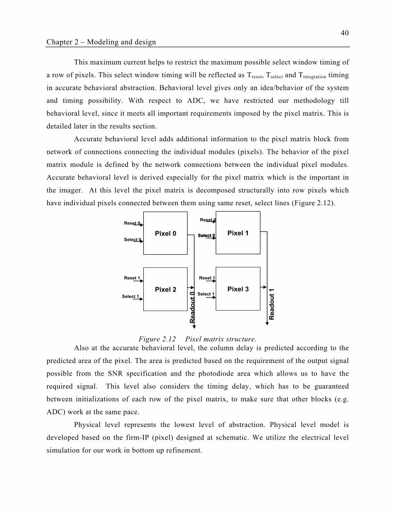
40
Chapter 2 – Modeling and design
This maximum current helps to restrict the maximum possible select window timing of
a row of pixels. This select window timing will be reflected as Treset, Tselect and Tintegration timing
in accurate behavioral abstraction. Behavioral level gives only an idea/behavior of the system
and timing possibility. With respect to ADC, we have restricted our methodology till
behavioral level, since it meets all important requirements imposed by the pixel matrix. This is
detailed later in the results section.
Accurate behavioral level adds additional information to the pixel matrix block from
network of connections connecting the individual modules (pixels). The behavior of the pixel
matrix module is defined by the network connections between the individual pixel modules.
Accurate behavioral level is derived especially for the pixel matrix which is the important in
the imager. At this level the pixel matrix is decomposed structurally into row pixels which
have individual pixels connected between them using same reset, select lines (Figure 2.12).
Figure 2.12 Pixel matrix structure.
Also at the accurate behavioral level, the column delay is predicted according to the
predicted area of the pixel. The area is predicted based on the requirement of the output signal
possible from the SNR specification and the photodiode area which allows us to have the
required signal. This level also considers the timing delay, which has to be guaranteed
between initializations of each row of the pixel matrix, to make sure that other blocks (e.g.
ADC) work at the same pace.
Physical level represents the lowest level of abstraction. Physical level model is
developed based on the firm-IP (pixel) designed at schematic. We utilize the electrical level
simulation for our work in bottom up refinement.
Pixel 0
Pixel 2
Pixel 1
Pixel 3
Reset 0
Reset 1 Reset 1
Reset 0
Select 0Select 0
Select 1
Select 0
Select 1
Read
ou
t 0
Read
ou
t 1
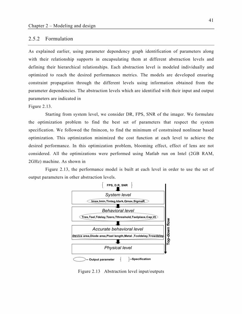
41
Chapter 2 – Modeling and design
2.5.2 Formulation
As explained earlier, using parameter dependency graph identification of parameters along
with their relationship supports in encapsulating them at different abstraction levels and
defining their hierarchical relationships. Each abstraction level is modeled individually and
optimized to reach the desired performances metrics. The models are developed ensuring
constraint propagation through the different levels using information obtained from the
parameter dependencies. The abstraction levels which are identified with their input and output
parameters are indicated in
Figure 2.13.
Starting from system level, we consider DR, FPS, SNR of the imager. We formulate
the optimization problem to find the best set of parameters that respect the system
specification. We followed the fmincon, to find the minimum of constrained nonlinear based
optimization. This optimization minimized the cost function at each level to achieve the
desired performance. In this optimization problem, blooming effect, effect of lens are not
considered. All the optimizations were performed using Matlab run on Intel (2GB RAM,
2GHz) machine. As shown in
Figure 2.13, the performance model is built at each level in order to use the set of
output parameters in other abstraction levels.
Behavioral level
Accurate behavioral level
Physical level
System level
To
p-d
ow
n f
low
FPS, D.R, SNR
Imax,Imin,Tinteg,Idark,Qmax,SigmaR
Tres,Tsel,Tdelay,Tzero,Tthreshold,Tselplace,Cap,Vt
Device area,Diode area,Pixel length,Metal ,Tcoldelay,Trowdelay
-- Output parameter --Specification
Figure 2.13 Abstraction level input/outputs

42
Chapter 2 – Modeling and design
2.6 Results
2.6.1 Pixel matrix
Pixel matrix block is segregated into three abstraction levels namely 1. System level 2.
Behavioral level 3. Accurate behavioral level. Their results are discussed in different sections.
2.6.1.1 System level
At the system level (2.1) and (2.2) are considered. The parameters such as Qmax,
Tintegration, Idark and readout noise values are optimized to achieve the D.R, FPS and SNR
performances. Table 2-1 represents the parameters which were obtained at the end of 36
iterations achieving the required performances. The cost function (2.3) takes into account all
performance tradeoffs using the weighted sum method. The cost function optimization graph is
indicated in Figure 2.14. Values obtained for parameters (ex.Qmax) will then be used as
specification to charascterize the pixel matrix in lower levels. The cost function for system
level is = . + . + . --(2.3)
Where α,β and γ are weighting parameters.
The problem formulation is as follows: For e.g dynamic range (performance) (2.1) is a
function of maximum (Imax), minimum current (Imin), readnoise , integration time(Tinteg) and
full well capacity (Qmax). We optimize these design variables to achieve the desired
performance metrics. These design variables are constrained by bounds as indicated in Table
2-1(A).
Table 2-1 System level input and outputs
(A) OPTIMISED PARAMETER INPUT (B) PERFORMANCE RESULT
Parameters Constraint Values
Tinteg <29us 28.2899us
Idark <10fA 1.03628E-16A
Read noise <10e- 10e-
Qmax <50000 17659.1e-
Imax 0.999998nA
Imin 56.6332fA
Performance Spec Result
Dynamic range >60dB 64.9386dB
Signal to noise ratio40-50dB42.4452dB
FPS 25 25
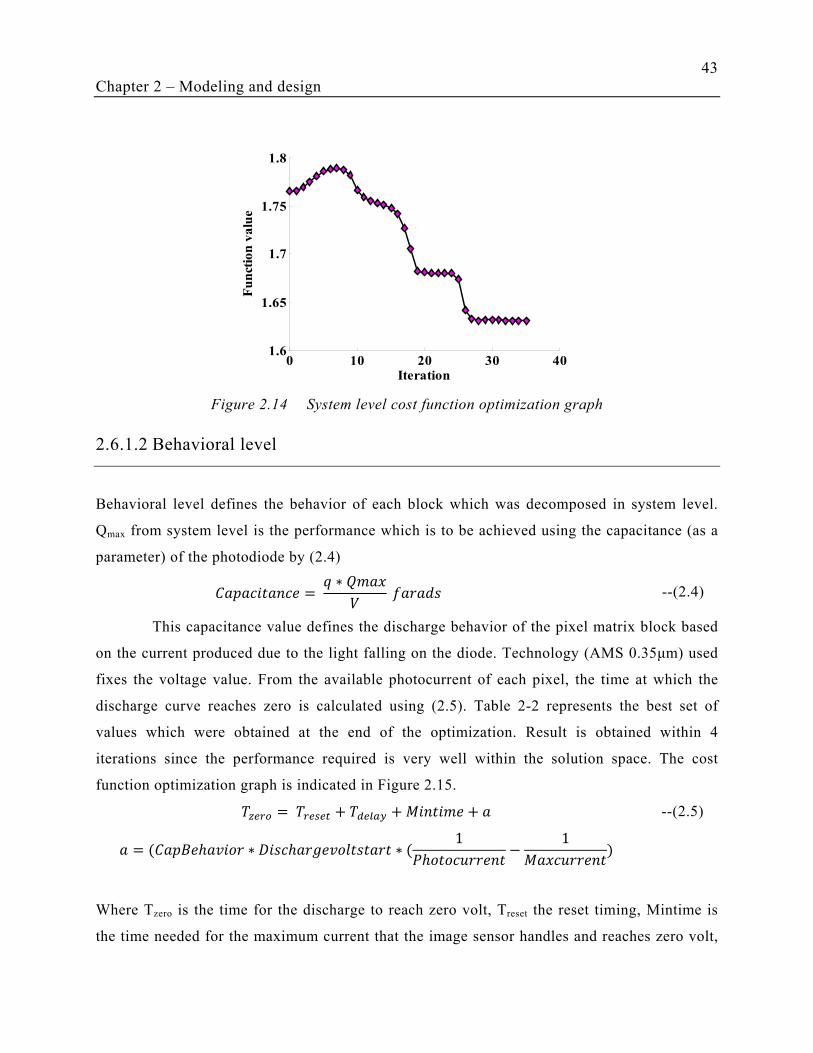
43
Chapter 2 – Modeling and design
0 10 20 30 401.6
1.65
1.7
1.75
1.8
Iteration
Fu
nct
ion
va
lue
Figure 2.14 System level cost function optimization graph
2.6.1.2 Behavioral level
Behavioral level defines the behavior of each block which was decomposed in system level.
Qmax from system level is the performance which is to be achieved using the capacitance (as a
parameter) of the photodiode by (2.4)
= ∗ --(2.4)
This capacitance value defines the discharge behavior of the pixel matrix block based
on the current produced due to the light falling on the diode. Technology (AMS 0.35µm) used
fixes the voltage value. From the available photocurrent of each pixel, the time at which the
discharge curve reaches zero is calculated using (2.5). Table 2-2 represents the best set of
values which were obtained at the end of the optimization. Result is obtained within 4
iterations since the performance required is very well within the solution space. The cost
function optimization graph is indicated in Figure 2.15. !"#$% = !$#&#' + !(#)*+ + , +
= (.ℎ0 ∗ ℎ102 ∗ ( 1ℎ4 − 1,4)
--(2.5)
Where Tzero is the time for the discharge to reach zero volt, Treset the reset timing, Mintime is
the time needed for the maximum current that the image sensor handles and reaches zero volt,
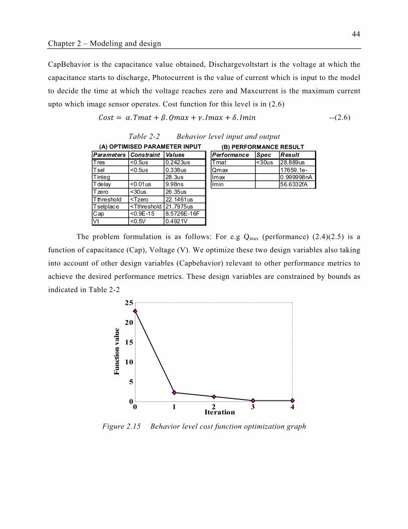
44
Chapter 2 – Modeling and design
CapBehavior is the capacitance value obtained, Dischargevoltstart is the voltage at which the
capacitance starts to discharge, Photocurrent is the value of current which is input to the model
to decide the time at which the voltage reaches zero and Maxcurrent is the maximum current
upto which image sensor operates. Cost function for this level is in (2.6) = . ! + . + . 7 + 8. 7 --(2.6)
Table 2-2 Behavior level input and output
(A) OPTIMISED PARAMETER INPUT (B) PERFORMANCE RESULT
Performance Spec Result
Tmat <30us 28.889us
Qmax 17659.1e-
Imax 0.999998nA
Imin 56.6332fA
Parameters Constraint Values
Tres <0.5us 0.2423us
Tsel <0.5us 0.338us
Tinteg 28.3us
Tdelay <0.01us 9.98ns
Tzero <30us 26.35us
Tthreshold <Tzero 22.1461us
Tselplace <Tthreshold 21.7975us
Cap <0.9E-15 8.5726E-16F
Vt <0.5V 0.4921V
The problem formulation is as follows: For e.g Qmax (performance) (2.4)(2.5) is a
function of capacitance (Cap), Voltage (V). We optimize these two design variables also taking
into account of other design variables (Capbehavior) relevant to other performance metrics to
achieve the desired performance metrics. These design variables are constrained by bounds as
indicated in Table 2-2
0 1 2 3 40
5
10
15
20
25
Iteration
Fu
nct
ion
valu
e
Figure 2.15 Behavior level cost function optimization graph
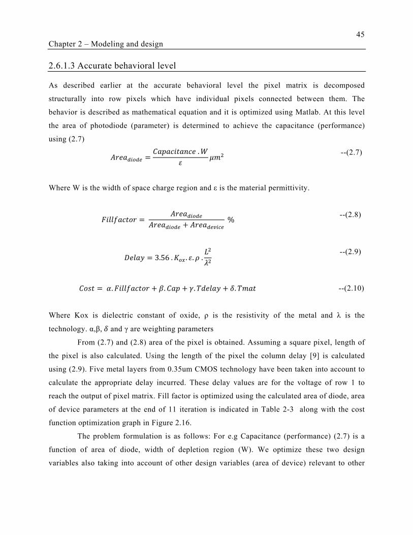
45
Chapter 2 – Modeling and design
2.6.1.3 Accurate behavioral level
As described earlier at the accurate behavioral level the pixel matrix is decomposed
structurally into row pixels which have individual pixels connected between them. The
behavior is described as mathematical equation and it is optimized using Matlab. At this level
the area of photodiode (parameter) is determined to achieve the capacitance (performance)
using (2.7)
9(:%(# = . ;< => --(2.7)
Where W is the width of space charge region and ε is the material permittivity.
22 = 9(:%(#9(:%(# + 9(#?:@# %
--(2.8)
2B = 3.56 . F%G . <. H . I>J>
--(2.9)
= . 22 + . + . ! 2B + 8. !
--(2.10)
Where Kox is dielectric constant of oxide, ρ is the resistivity of the metal and λ is the
technology. α,β, 8 and γ are weighting parameters
From (2.7) and (2.8) area of the pixel is obtained. Assuming a square pixel, length of
the pixel is also calculated. Using the length of the pixel the column delay [9] is calculated
using (2.9). Five metal layers from 0.35um CMOS technology have been taken into account to
calculate the appropriate delay incurred. These delay values are for the voltage of row 1 to
reach the output of pixel matrix. Fill factor is optimized using the calculated area of diode, area
of device parameters at the end of 11 iteration is indicated in Table 2-3 along with the cost
function optimization graph in Figure 2.16.
The problem formulation is as follows: For e.g Capacitance (performance) (2.7) is a
function of area of diode, width of depletion region (W). We optimize these two design
variables also taking into account of other design variables (area of device) relevant to other
46
Chapter 2 – Modeling and design
performance (Fillfactor) to achieve the desired capacitance performance. These design
variables are constrained by bounds as indicated in Table 2-3
Table 2-3 Accurate behavioral level input and output
(A) OPTIMISED PARAMETER INPUT (B) PERFORMANCE RESULTParameters Constraint Values
Area_device 19um2
Area_diode 28.4837um2
Pixelarea 47.4729um2
Length_pixel 6.8901um
Tcoldelay1 2.2703E-21s
Tcoldelay2 2.185E-21s
Tcoldelay3 1.8045E-21s
Performance Spec Result
Cap 8.57E-16F
Tmat 27.9us
fillfactor <0.6 0.5999.
Tdelay 9.98ns
0 2 4 6 8 10 120
0.1
0.2
0.3
0.4
0.5
Iteration
Fu
nct
ion
va
lue
Figure 2.16 Accurate behavior level cost function optimization graph
2.6.2 ADC - Results
In this part we will discuss the ADC modeling results. ADC is segregated into system level and
behavioral abstraction levels. At the behavioral level we divide the ADC into two sub-blocks
namely DAC and comparator. These abstraction levels and their relevant results are explained
below.

47
Chapter 2 – Modeling and design
2.6.2.1 System level -----------------------------------------------------------------------------------------------------------------
Overall ADC system performance is based on few performances such as the signal to noise
performance, sampling rate etc., But ADC is not limited only by these performances. Sampling
rate of the ADC is imposed by the pixel matrix frames per second requirement. This is taken at
this level of ADC.
The Signal to Noise Ratio is the ratio between the power of the signal and the total
noise produced by quantization and the noise of the circuit. The SNR accounts for the noise in
the entire Nyquist interval. It may depend on the frequency of the input signal but normally it
is constant in the Nyquist zone and it decreases proportional to the input amplitude, resolution
and sampling frequency. At the system level the SNR can be calculated by (2.11) [12]:
= 20 log P 2Q ∗ 2√2S . --(2.11)
Where = T21 > + > + 4U > --(2.12)
Following are the different noise sources possible in ADC [12][13]: Sampling noise is
dependent on temperature and the capacitance C0. It is given by (2.13) 21 = √2. F. !/W --(2.13)
Followed by (2.14) = √2. B. 3 . --(2.14)
Where
3 . = 0.69. (24 + 1)(2. Y. 0.5. 2Z) --(2.15)
Amplitude quantization is the change of a sampled data signal from continuous level
to discrete level. The dynamic range of the ideal quantizer is divided into a number of equal
quantization intervals, each of which is represented by a given analog amplitude. An input
amplitude that resides within a certain quantization interval is converted to the analog
amplitude representing this interval. Often the value representing a quantization interval is the
mid-point of the interval.
48
Chapter 2 – Modeling and design
4U = 2[√12 --(2.16)
The following relation is the maximum achievable (2.17) SNR in relation to the
number of bits of the quantizer for a sinusoidal input.
!ℎ2 = 6.02 . 24 + 1.78 --(2.17)
Normally the practically available SNR in the system is lower than the theoretical SNR
obtained. This can be used to ensure that the practical SNR obtained during optimization is
correct.
The maximum achievable SNR is also called signal-to-quantization noise ratio. The
equation below reveals that every added bit of resolution increases the SNR by 6 dB.
Accordingly, the power of quantization error decreases by a factor of 4. But since this equation
accounts only for quantization noise, a more general form is used to consider all possible noise
sources defining the equivalent or the effective number of bits (ENOB) of the ADC and is
given by (2.18)
^_. = − 1.786.02 --(2.18)
Another performance which is important for ADC is the bandwidth. Bandwidth
depends mainly on the resolutions and sampling rate. It is given by (2.19)
. ` ℎ = 12Z aU --(2.19)
Where
2Z = 121 . (24 + 1) --(2.20)
These above equations give the basic performance metrics of the ADC operation at
system level. Overall ADC system performance and its results are presented here. The
optimizations is performed in Matlab. The system level cost function is formulated as the
weighted sum of the performance requirement as in (2.21)
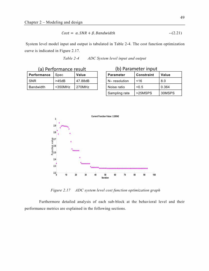
49
Chapter 2 – Modeling and design
= . + . . ` ℎ --(2.21)
System level model input and output is tabulated in Table 2-4. The cost function optimization
curve is indicated in Figure 2.17.
Furthermore detailed analysis of each sub-block at the behavioral level and their
performance metrics are explained in the following sections.
Performance Spec Value
SNR >45dB 47.88dB
Bandwidth <350MHz 270MHz
Parameter Constraint Value
N– resolution <16 8.0
Noise ratio <0.5 0.364
Sampling rate >25MSPS 30MSPS
(a) Performance result (b) Parameter input
Table 2-4 ADC System level input and output
0 10 20 30 40 50 60 70 80 90 1002.2
2.3
2.4
2.5
2.6
2.7
2.8
2.9
3
Iteration
Fu
nc
tio
n v
alu
e
Current Function Value: 2.26542
Figure 2.17 ADC system level cost function optimization graph

50
Chapter 2 – Modeling and design
2.6.2.2 Behavioral level – DAC
This DAC [10] is an array of binary weighted capacitors plus one additional capacitor of
weight corresponding to the last significant bit (LSB), and switches that connect the capacitor
bottom plates to three different voltages: VDD, Vref and ground. For a n-bit DAC, the value of
the capacitors are as per (2.22) : = 2:bc . W , ∈ f1 … . . i --(2.22)
The capacitor banks will be used as track and hold block as well. The capacitor array
is used to acquire the analog signal during the sampling phase. Such a usage reduces power
consumption due to a switch and a capacitor [11]. In order to use directly the DAC capacitors,
the sampling frequency is set as a performance to be achieved to have a relative high
impedance. The time constant required for charging the capacitor array is given by (2.23) j = . '%'*) --(2.23)
Where '%'*) = W. 2Q --(2.24)
Where, N is resolution of ADC. From the above expression we could calculate the minimum
period is expressed as (2.25)
!k:l = j. 2 1< --(2.25)
Where < is the error. The maximum error that we can tolerate is half of the LSB.
mno = 2Q --(2.26)
From the above calculations it is possible to obtain the sampling rate which is the
required performance given in (2.27)
21 = 19. !k:l --(2.27)
The energy consumed by the DAC is calculated (2.28) based on the sampling rate followed by
power calculation (2.29)
^1Bpqr = 12 . '%'*) . > --(2.28)
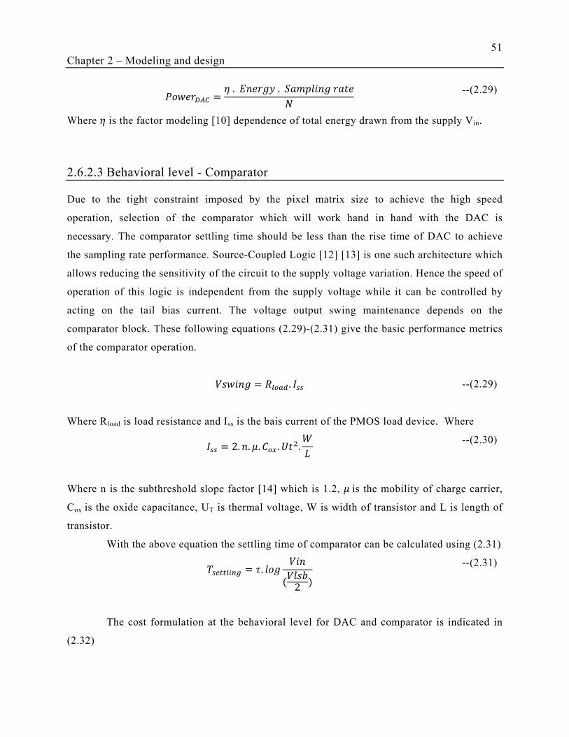
51
Chapter 2 – Modeling and design
`pqr = s . ^1B . 21 --(2.29)
Where s is the factor modeling [10] dependence of total energy drawn from the supply Vin.
2.6.2.3 Behavioral level - Comparator
Due to the tight constraint imposed by the pixel matrix size to achieve the high speed
operation, selection of the comparator which will work hand in hand with the DAC is
necessary. The comparator settling time should be less than the rise time of DAC to achieve
the sampling rate performance. Source-Coupled Logic [12] [13] is one such architecture which
allows reducing the sensitivity of the circuit to the supply voltage variation. Hence the speed of
operation of this logic is independent from the supply voltage while it can be controlled by
acting on the tail bias current. The voltage output swing maintenance depends on the
comparator block. These following equations (2.29)-(2.31) give the basic performance metrics
of the comparator operation.
`1 = )%*( . 7&& --(2.29)
Where Rload is load resistance and Iss is the bais current of the PMOS load device. Where
7&& = 2. . =. %G . t>. ;I --(2.30)
Where n is the subthreshold slope factor [14] which is 1.2, = is the mobility of charge carrier,
Cox is the oxide capacitance, UT is thermal voltage, W is width of transistor and L is length of
transistor.
With the above equation the settling time of comparator can be calculated using (2.31)
!&#''):lu = j. 21 (2[2 ) --(2.31)
The cost formulation at the behavioral level for DAC and comparator is indicated in
(2.32)
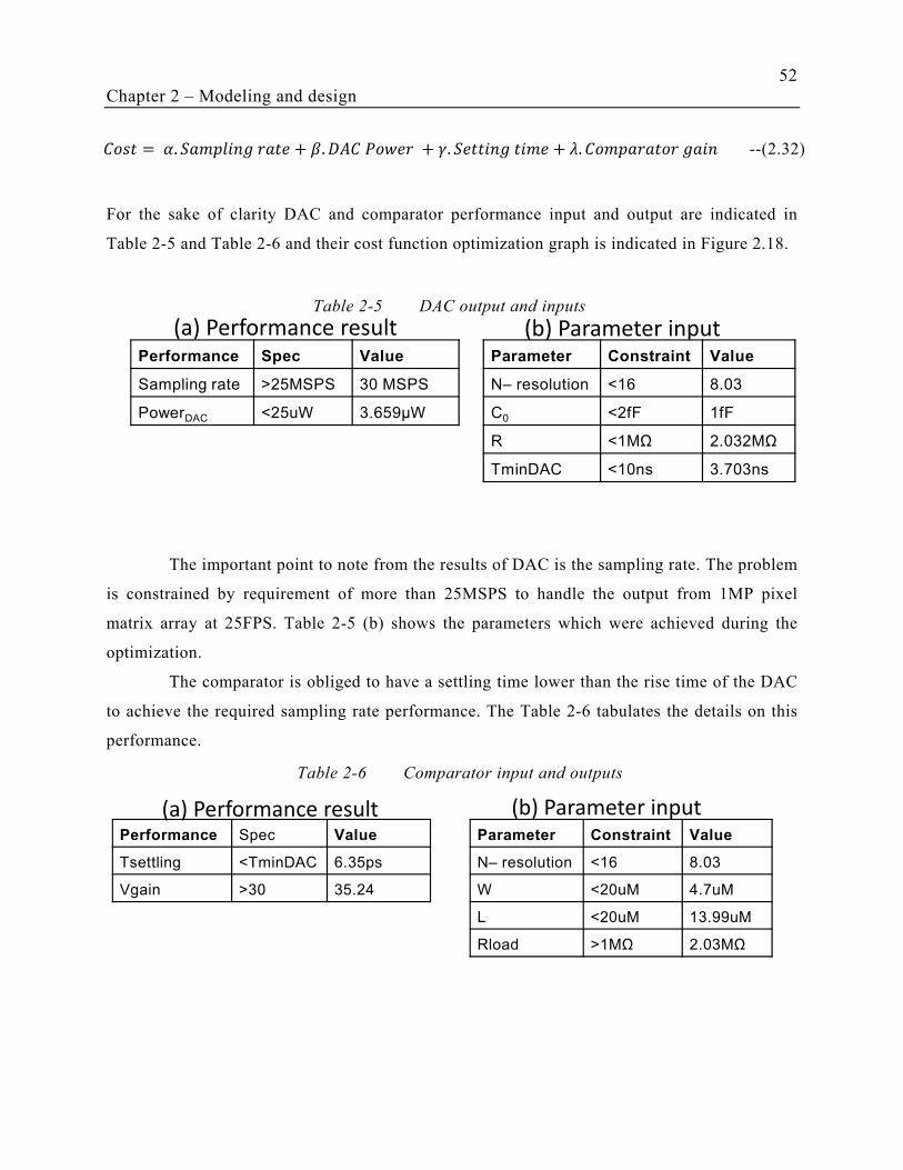
52
Chapter 2 – Modeling and design
= . 21 + . 9 ` + . 1 + J. 1 --(2.32)
For the sake of clarity DAC and comparator performance input and output are indicated in
Table 2-5 and Table 2-6 and their cost function optimization graph is indicated in Figure 2.18.
The important point to note from the results of DAC is the sampling rate. The problem
is constrained by requirement of more than 25MSPS to handle the output from 1MP pixel
matrix array at 25FPS. Table 2-5 (b) shows the parameters which were achieved during the
optimization.
The comparator is obliged to have a settling time lower than the rise time of the DAC
to achieve the required sampling rate performance. The Table 2-6 tabulates the details on this
performance.
Performance Spec Value
Tsettling <TminDAC 6.35ps
Vgain >30 35.24
Parameter Constraint Value
N– resolution <16 8.03
W <20uM 4.7uM
L <20uM 13.99uM
Rload >1MΩ 2.03MΩ
(a) Performance result (b) Parameter input
Table 2-5 DAC output and inputs
Table 2-6 Comparator input and outputs
Performance Spec Value
Sampling rate >25MSPS 30 MSPS
PowerDAC <25uW 3.659µW
Parameter Constraint Value
N– resolution <16 8.03
C0 <2fF 1fF
R <1MΩ 2.032MΩ
TminDAC <10ns 3.703ns
(a) Performance result (b) Parameter input
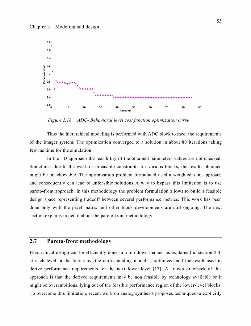
53
Chapter 2 – Modeling and design
Thus the hierarchical modeling is performed with ADC block to meet the requirements
of the Imager system. The optimization converged to a solution in about 80 iterations taking
few ms time for the simulation.
In the TD approach the feasibility of the obtained parameters values are not checked.
Sometimes due to the weak or infeasible constraints for various blocks, the results obtained
might be unachievable. The optimization problem formulated used a weighted sum approach
and consequently can lead to unfeasible solutions A way to bypass this limitation is to use
pareto-front approach. In this methodology the problem formulation allows to build a feasible
design space representing tradeoff between several performance metrics. This work has been
done only with the pixel matrix and other block developments are still ongoing. The next
section explains in detail about the pareto-front methodology.
2.7 Pareto-front methodology
Hierarchical design can be efficiently done in a top-down manner as explained in section 2.4:
at each level in the hierarchy, the corresponding model is optimized and the result used to
derive performance requirements for the next lower-level [17]. A known drawback of this
approach is that the derived requirements may be non feasible by technology available or it
might be overambitious, lying out of the feasible performance region of the lower-level blocks.
To overcome this limitation, recent work on analog synthesis proposes techniques to explicitly
0 10 20 30 40 50 60 70 80 902.2
2.4
2.6
2.8
3
3.2
3.4
3.6
3.8
Iteration
Fu
nc
tio
n v
alu
e
Figure 2.18 ADC- Behavioral level cost function optimization curve
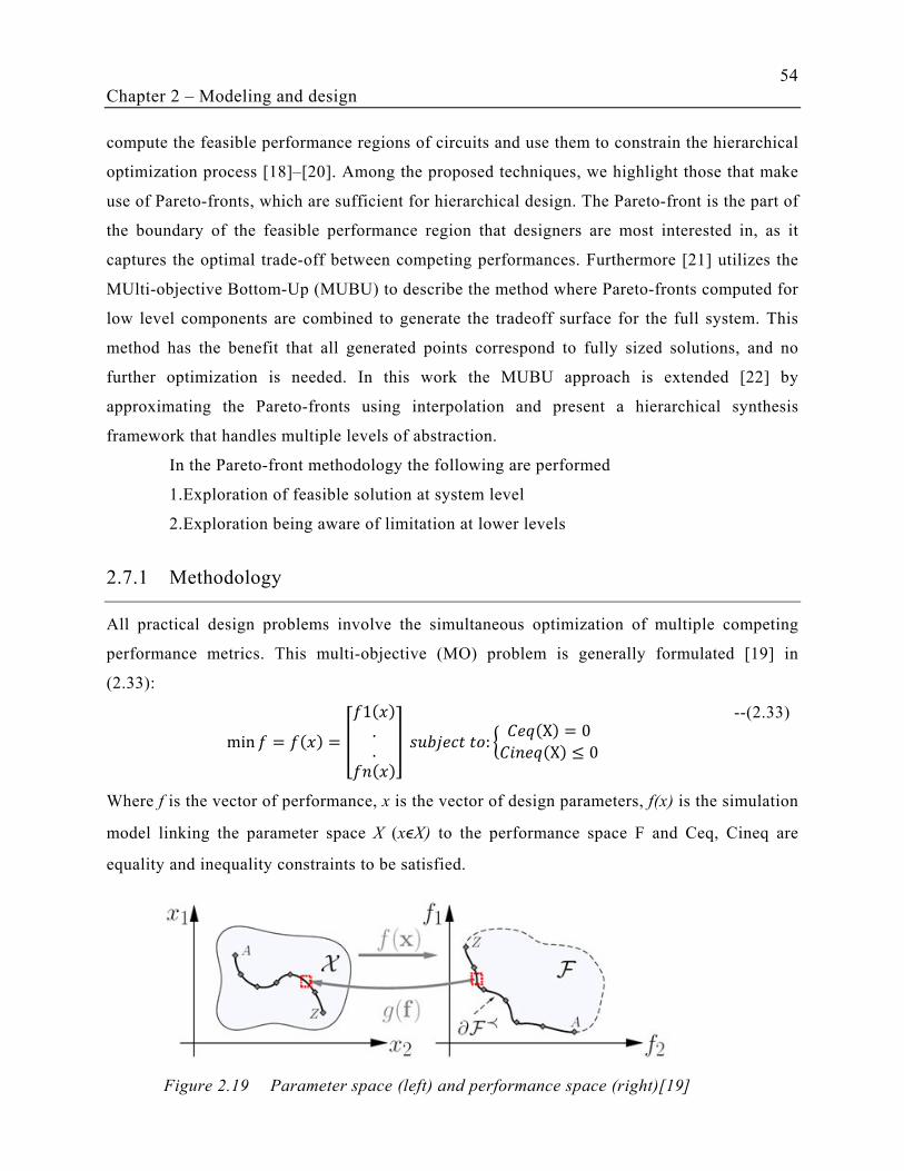
54
Chapter 2 – Modeling and design
compute the feasible performance regions of circuits and use them to constrain the hierarchical
optimization process [18]–[20]. Among the proposed techniques, we highlight those that make
use of Pareto-fronts, which are sufficient for hierarchical design. The Pareto-front is the part of
the boundary of the feasible performance region that designers are most interested in, as it
captures the optimal trade-off between competing performances. Furthermore [21] utilizes the
MUlti-objective Bottom-Up (MUBU) to describe the method where Pareto-fronts computed for
low level components are combined to generate the tradeoff surface for the full system. This
method has the benefit that all generated points correspond to fully sized solutions, and no
further optimization is needed. In this work the MUBU approach is extended [22] by
approximating the Pareto-fronts using interpolation and present a hierarchical synthesis
framework that handles multiple levels of abstraction.
In the Pareto-front methodology the following are performed
1.Exploration of feasible solution at system level
2.Exploration being aware of limitation at lower levels
2.7.1 Methodology
All practical design problems involve the simultaneous optimization of multiple competing
performance metrics. This multi-objective (MO) problem is generally formulated [19] in
(2.33):
min = () = y1()..()z 4[ : (X) = 0(X) ≤ 0i --(2.33)
Where f is the vector of performance, x is the vector of design parameters, f(x) is the simulation
model linking the parameter space X (xϵX) to the performance space F and Ceq, Cineq are
equality and inequality constraints to be satisfied.
Figure 2.19 Parameter space (left) and performance space (right)[19]

55
Chapter 2 – Modeling and design
Solving the above equation leads to Pareto-optimal designs. Always improving one
performance comes at the cost of other. The outcome of all these optimal designs is the so
called Pareto-frontier. The approach presented next consists of characterizing the Pareto-front
of a block by computing a few optimal designs and then generating interpolation functions g(f)
to predict the optimal design for different performance requirements (Figure 2.19).
The simulation of a model can give access to multiple performance metrics (e.g: FPS,
DR, SNR, Area etc). Sometimes not all the performances are competing or of main interest for
the design process. Using this knowledge on the architecture at hand, the designer decides
which metrics can be excluded from the analysis, ending up with a subset that we will call the
trade-off performances.
To visualize the performance evolution several constraints were applied in the
optimization. Constraints are used with two goals: ensure the proper operation of the
component and confine the trade-off analysis to a region of interest.After identifying the
performances to be solved and applying the appropriate constraints we were able to compute
the pareto optimal design. This is explained in the next section along with supporting results.
2.7.2 Pixel pareto-front - Results
To produce the pixel pareto-front, Dynamic range (DR), Signal to noise ratio (SNR) and Area
performances are taken into account to prove the pareto-front methodology in the design flow.
Additional performances could be added easily following the same procedure.
DR is expressed using (2.34)
dB
σonTintegrati*Idark*q
1
onTintegrati
q
IdarkonTintegrati
qQmax
20logImin
Imax20logD.R
2
r
1010
+
−
==
--(2.34)
where q is the charge of electrons, Qmax is the full well capacity expressed in electrons,
Tintegration is the integration time in seconds, Idark is the dark current in Amperes, is the
read noise in electrons. Assuming Idark equal to 1fA and read noise as 10e- the following
output curves is obtained as in Figure 2.20. This curve is an illustration of DR (performance)
evolution as a function of Tintegration and Full well capacity (parameters).
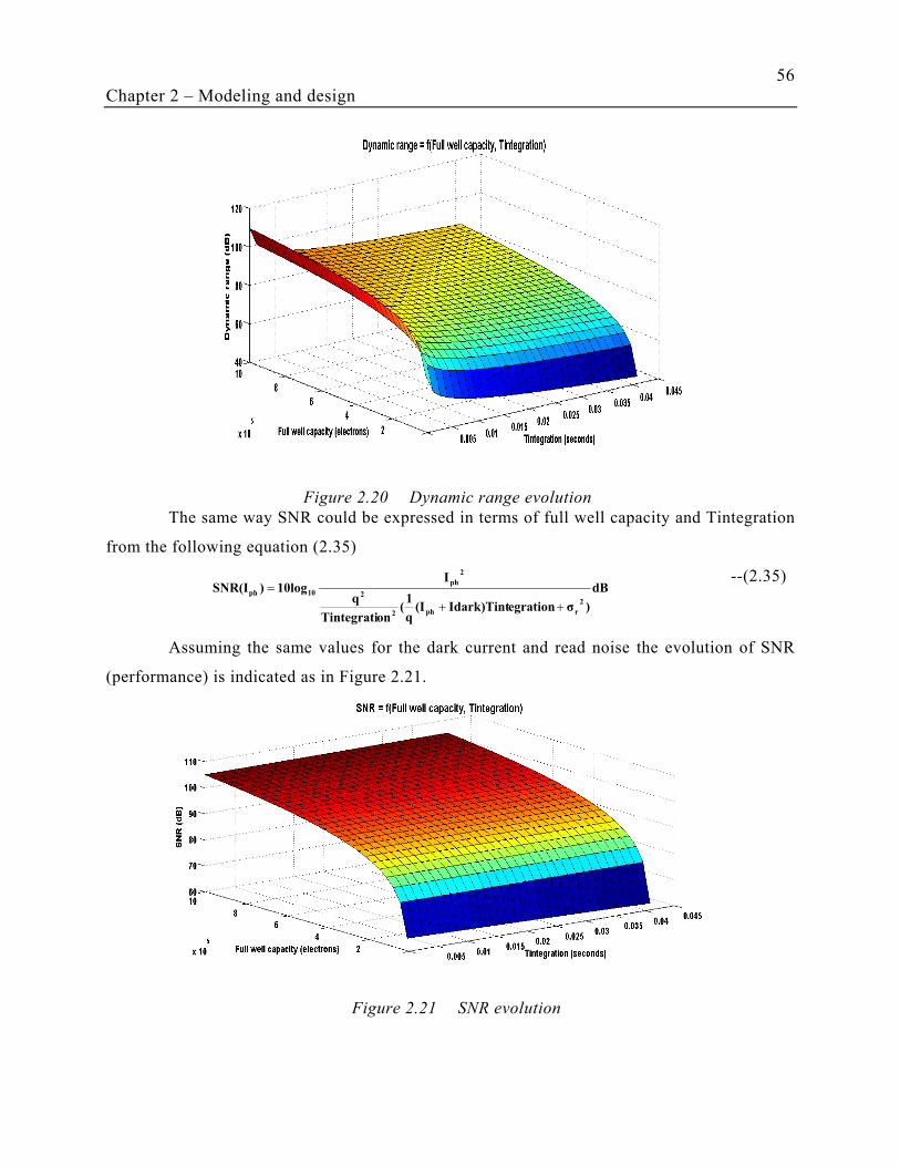
56
Chapter 2 – Modeling and design
The same way SNR could be expressed in terms of full well capacity and Tintegration
from the following equation (2.35)
dB
)σegrationIdark)Tint(Iq
1(
onTintegrati
q
I10log)SNR(I
2
rph2
2
2
ph
10ph
++
=
--(2.35)
Assuming the same values for the dark current and read noise the evolution of SNR
(performance) is indicated as in Figure 2.21.
Figure 2.20 Dynamic range evolution
Figure 2.21 SNR evolution
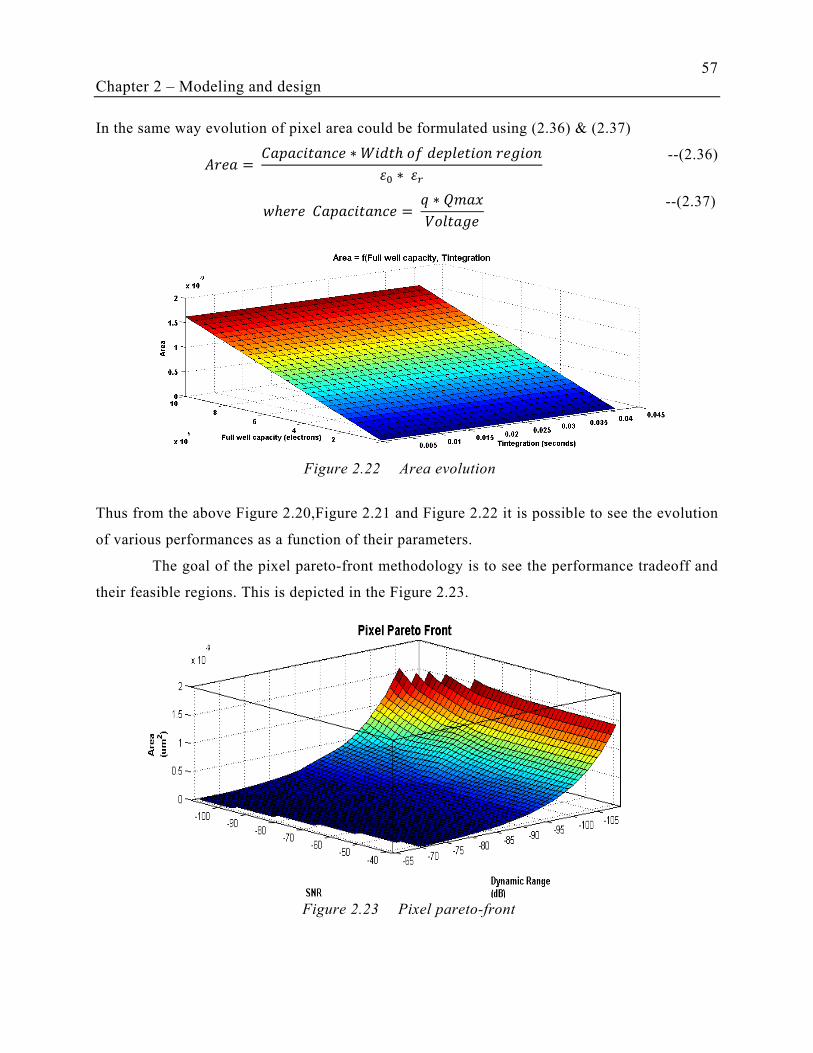
57
Chapter 2 – Modeling and design
In the same way evolution of pixel area could be formulated using (2.36) & (2.37)
9 = ∗ ; ℎ 2 1<W ∗ <$ --(2.36)
`ℎ = ∗ 21
--(2.37)
Thus from the above Figure 2.20,Figure 2.21 and Figure 2.22 it is possible to see the evolution
of various performances as a function of their parameters.
The goal of the pixel pareto-front methodology is to see the performance tradeoff and
their feasible regions. This is depicted in the Figure 2.23.
Figure 2.23 Pixel pareto-front
Figure 2.22 Area evolution
58
Chapter 2 – Modeling and design
The above figure clearly shows the entire region of operational feasibility for the pixel
respecting all the constraints imposed during the optimization. It also provides an alternate
methodology to understand the tradeoff between competing performances and selection. This
methodology gives much more realistic behavior of the system compared to the top-down
approach.
2.8 Conclusion
The modeling approach followed during this research work accomplished the following:
Top-down design methodology
Hierarchical approach realized using
Parameter dependency graphs
Pixel performances studied extensively
Segregated into various abstraction levels
Achieved the required performances along with cost function
Hierarchical top-down approach in ADC
Achieved the necessary performance imposed by pixel matrix
Pareto-front methodology
• Pixel matrix block utilized to prove the methodology
• Tradeoff between various performances has been evaluated
• Ongoing work with other blocks
The above modeling work has extensively studied the details of top-down to
synthesize various blocks. During the TD approach, the temperature used is ambient condition
(300K) due to the lack of information on discharge behavior based on temperature. Firstly, in a
realistic situation imager operates at temperature higher than ambient condition. Secondly,
moving to 3D architecture creates hotspots. So the problem of inter-pixel variability gets
aggravated. There are no scalable high level models to simulate pixel matrix giving importance
to inter-pixel variability. To have an accurate model at system level we follow the bottom-up
refinement approach to collect data from electrical level and feed back at system level. This
improves the accuracy of system level model with respect to temperature. in the research arena

59
Chapter 2 – Modeling and design
on a model looking at thermal aspects in 3D architecture specialized in imager. Next chapters
will mainly focus on
• Modeling:
• Modeling of pixel matrix to analyze thermal impact (Bottom-up)
• Novel (scalable) model capable of simulating huge matrix (For ex. 0.5 MP
or more)
• High speed simulation capability
• 3D Integrated design flow
• Floorplanning
• Thermal simulation
• High speed simulation of pixel matrix with thermal model
The next chapters will be focusing on the above aspects and will give deeper insights
into the 3D-Imager especially in thermal aspect based floorplanning and in finding solution
which might deteriorate the performance of the imager.
60
Chapter 2 – Modeling and design
Bibliography
[1] M.Torngren et al, « Component-based and Model based development: A
comparison in the context of embedded systems” Proceeding of
EUROMICRO’05 pp:432-441
[2] R Stevens, P Brook, K Jackson & S Arnold. Systems Engineering - coping
with complexity. Pearson Education 1998. ISBN 0-13-095085-8
[3] F Neelamkavil. Computer simulation and modelling. John Wiley & Sons Inc,
1987
[4] V.Viswanathan, L.Labrak,F.Frantz, D.Navarro and I.O’Connor, “Model based
design of Imager using abstraction segregated parameter dependency graphs”,
Newcas 2011, June 26-29, Bordeaux, France
[5] L.Labrak, I.O’Connor, “Heterogeneous System Design Platform and
Perspectives for 3D integration”, 21th IEEE International Conference on
Microelectronics ICM'09, Marrakech, Morocco, 2009
[6] M.Bigas et al, “Review of CMOS image Sensors” Microelectronic
Journal,2006,37,433-451
[7] E.R. Fossum, “Active Pixel Sensors(APS)- Are CCDs Dinosaurs?” Proc.SPIE
vol.1900,pp.2-14, 1992
[8] A.El Gamal “High dynamic range image sensors” lectures and classnotes,
Standford university
[9] http://www.maxim-ic.com/appnotes.cfm/an_pk/1080/, 21 juin 2009.
[10] B. P. Ginsburg and A. Chandrakasan, “An energy-effcient charge
recyclingapproach for a SAR converter with capacitive DAC," in IEEE
ISCAS Int.Symp. Circuits and Systems, 2005, pp. 184-187.
[11] G.Beanato, “Design of very low power SAR analog to digital converter”,
thesis, 14 August 2009
[12] A. Tajalli, E. J. Brauer, Y.Leblebici “Ultra-low power 32-bit pipelined adder
using subthreshold source-coupled logic with 5 fJ/stage PDP”
Microelectronics Journal 40 (2009) 973-978.
61
Chapter 2 – Modeling and design
[13] A. Tajalli, Elizabeth J. Brauer et al., “Subthreshold Source-Coupled Logic
Circuits for Ultra-Low-Power Applications”, IEEE J. Solid-State Circuits,
vol. 43, no.7, pp. 1699-1710, July 2008.
[14] http://www.iue.tuwien.ac.at/phd/stockinger/node13.html
[15] Mootaz, “Systematic design of SAR Analog to digital converter, Thesis,
Cairo university, 2008
[16] http://www.lte.e-technik.uni-rlangen.de/download/ADU/Converter_class4.pdf
[17] H. Chang, E. Charbon, U. Choudhury, A. Demir, E. Felt, E. Liu,E. Malavasi,
A. Sangiovanni-Vincentelli, and I. Vassiliou, A Top-Down, Constraint-
Driven Design Methodology for Analog Integrated Circuits.Springer, 1996.
[18] P. Nuzzo, X. Sun, C.-C. Wu, F. D. Bernardinis, and A. Sangiovanni-
Vincentelli, “A platform-based methodology for system-level mixedsignal
design,” EURASIP J. Embedded Syst., vol. 2010, pp. 6:4–6:4,January 2010.
[19] G. Stehr, H. Graeb, and K. Antreich, “Analog performance spaceexploration
by normal-boundary intersection and by fourier motzkin elimination,”
computer-Aided Design of Integrated Circuits and Systems, IEEE
Transactions on, vol. 26, no. 10, pp. 1733 –1748, oct. 2007.
[20] T. Eeckelaert, R. Schoofs, G. Gielen, M. Steyaert, and W. Sansen, “An
efficient methodology for hierarchical synthesis of mixed-signal systems with
fully integrated building block topology selection,” in Proceedings of the
conference on Design, automation and test in Europe, ser. DATE’07. San
Jose, CA, USA: EDA Consortium, 2007, pp. 81–86.
[21] G. Gielen, T. McConaghy, and T. Eeckelaert, “Performance spacemodeling
for hierarchical synthesis of analog integrated circuits,” in Proceedings of the
42nd annual Design Automation Conference, DAC ’05. New York, NY, USA:
ACM, 2005, pp. 881–886.
[22] Felipe Frantz, Lioua Labrak, Ian O'Connor, Hierarchical Design Flow for
Heterogeneous Systems using Pareto Front Interpolation, IEEE Transaction
on Computer Aided Design (TCAD), (under review)
Chapter 3
Thermal-aware image sensor model
3.1 Introduction
One of the unavoidable sources of pixel noise in 3D stacked CMOS imagers is thermal - both
in terms of absolute temperature for thermal noise, and in terms of imager-wide temperature
variation for inter-pixel variability. In the former case the thermal noise is generated by
random thermally induced motion of electrons. It exhibits [1] a zero-mean, flat and wide
bandwidth Gaussian power spectral density. Several analysis have been published [2][3][4] on
the absolute temperature impact on thermal noise. We are interested in proving and proposing
solutions for the inter-pixel variability due to the impact of temperature. This is important in
system level modeling perspective moving from 2D to 3D stacked chip. Although temperature
can be of some impact in 2D imagers, it is exacerbated in 3D imagers due to a higher overall
power density. Thermal noise also of course leads to greater performance degradation in 3D
chip. In order to minimize the thermal impact on the pixel matrix it is essential to analyze the
thermal problem in detail and provide possible solutions.
In this chapter, the thermal aware model generation for analyzing the thermal impact
is explained in detail. Firstly, the need for the model and the properties which have to be
fulfilled by the new model will be discussed in section 3.2. The model generation takes into
account exhaustive data generation from electrical simulations, as discussed in section 3.3.
With the obtained data, we describe the methodology used to create the thermal model in
section 3.4, followed by a pre-validation phase, discussed in section 3.5. The integration of the
pre-validated model into a SystemC-based modeling tool will be discussed in section 3.6. Post-
validation of the final model is discussed in section 3.7. In section 3.8, conclusions will be
drawn from the analysis made through several test cases.

63
Chapter 3 – Thermal-aware image sensor model
3.2 Thermal Model
3.2.1 Problems and requirements
Few tools exist to analyze the impact of temperature variation over different regions of the
entire pixel matrix on the output. Such analyses could give a clear picture of the impact of
temperature during the early stages of design space exploration. This is not feasible with
existing tools such as Spectre or PSpice, since these tools are very costly in terms of
computation time to simulate large (>1Mpixels) imager pixel matrices. Even more costly are
finite element method based tools (such as ANSYS), which require sophisticated meshing
methodologies and long simulation times for high-resolution simulation. It is not currently
feasible to simulate a complete matrix with this approach – instead, designers simulate
individual pixels or groups of pixels to analyze their behavior. Hence, system-level designers
face real difficulties in the development of simulation and modeling methods for fast, scalable
and accurate pixel matrix evaluation. The focus of research work for simulation and modeling
at high abstraction levels strive to overcome these problems. The main factors which are
targeted in this work are:
• Short simulation cycles (speed)
• Ability to simulate any pixel matrix size (scalability)
• Low error (a few %) when compared to electrical simulation results (accuracy)
Such a thermal model could offer the designer:
• More accurate verification of design decisions in terms of the pixel matrix
output
• Choice of technology parameters (silicon thickness, area, power etc.) based on
thermal impact
• Early and thermal aware floorplanning
• Hardware block specifications to apply correction (Correlated Double
Sampling (CDS), filters etc.)
• Introduction of thermal Fixed Pattern Noise (FPN) - Software based correction
algorithms applied only to regions which have higher thermal impact. This
could reduce the workload of ISP
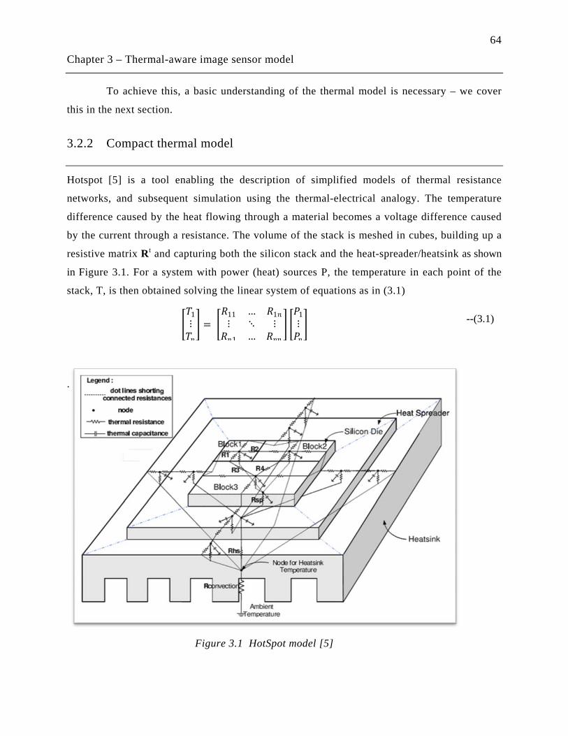
64
Chapter 3 – Thermal-aware image sensor model
To achieve this, a basic understanding of the thermal model is necessary – we cover
this in the next section.
3.2.2 Compact thermal model
Hotspot [5] is a tool enabling the description of simplified models of thermal resistance
networks, and subsequent simulation using the thermal-electrical analogy. The temperature
difference caused by the heat flowing through a material becomes a voltage difference caused
by the current through a resistance. The volume of the stack is meshed in cubes, building up a
resistive matrix Rt
Figure 3.1
and capturing both the silicon stack and the heat-spreader/heatsink as shown
in . For a system with power (heat) sources P, the temperature in each point of the
stack, T, is then obtained solving the linear system of equations as in (3.1)
𝑇𝑇1⋮𝑇𝑇𝑛𝑛 =
𝑅𝑅11 … 𝑅𝑅1𝑛𝑛⋮ ⋱ ⋮𝑅𝑅𝑛𝑛1 … 𝑅𝑅𝑛𝑛𝑛𝑛
𝑃𝑃1⋮𝑃𝑃𝑛𝑛
--(3.1)
.
Figure 3.1 HotSpot model [5]

65
Chapter 3 – Thermal-aware image sensor model
Although this model can aid in visualizing the temperature evolution across the layer,
based on the power density of each block and material properties available at each layer, an
imager thermal model requires more information to accurately evaluate discharge behavior,
which is dependent on:
• Temperature
• Light intensity
• Integration time
In our approach, we implement an imager thermal model with SystemC to include
description of discharge behavior based on light intensity and integration time, and couple this
to the HotSpot based compact modeling technique to obtain a temperature map, which is fed
into the imager thermal model. This integration of imager thermal model along with the
compact model is described in detail in Chapter 4. In the next step, we will go through the
imager thermal model development steps.
3.2.3 Model development steps
We follow a bottom-up (Figure 3.2) and empirical approach modeling to achieve an accurate
(but design-specific) high-level model. We qualify the approach as bottom-up because we
extract data from an existing circuit described at the transistor level; it is therefore intended to
be used in system validation steps or in system exploration steps (where free exploration
parameters are in blocks other than the imager). The approach is also empirical, because we
generate mathematical models from the data, without the use of any physical parameters, and
further without any preconception of the type of mathematical model to be used. Detailed
description on model and its characteristics is made in Chapter 2.
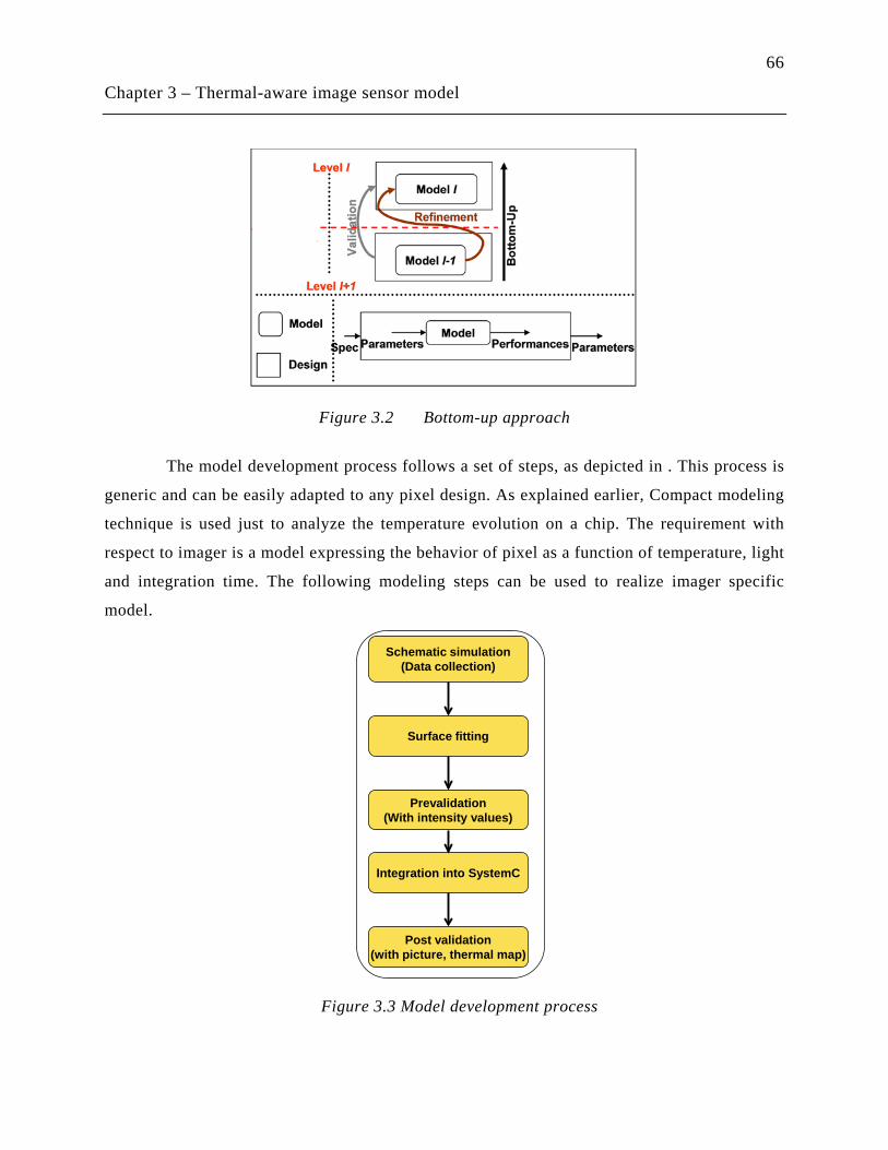
66
Chapter 3 – Thermal-aware image sensor model
Figure 3.2 Bottom-up approach
The model development process follows a set of steps, as depicted in . This process is
generic and can be easily adapted to any pixel design. As explained earlier, Compact modeling
technique is used just to analyze the temperature evolution on a chip. The requirement with
respect to imager is a model expressing the behavior of pixel as a function of temperature, light
and integration time. The following modeling steps can be used to realize imager specific
model.
Figure 3.3 Model development process
Schematic simulation(Data collection)
Surface fitting
Prevalidation(With intensity values)
Integration into SystemC
Post validation(with picture, thermal map)
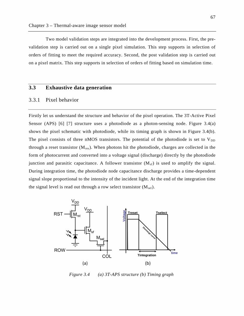
67
Chapter 3 – Thermal-aware image sensor model
Two model validation steps are integrated into the development process. First, the pre-
validation step is carried out on a single pixel simulation. This step supports in selection of
orders of fitting to meet the required accuracy. Second, the post validation step is carried out
on a pixel matrix. This step supports in selection of orders of fitting based on simulation time.
3.3 Exhaustive data generation
3.3.1 Pixel behavior
Firstly let us understand the structure and behavior of the pixel operation. The 3T-Active Pixel
Sensor (APS) [6] [7] structure uses a photodiode as a photon-sensing node. Figure 3.4(a)
shows the pixel schematic with photodiode, while its timing graph is shown in Figure 3.4(b).
The pixel consists of three nMOS transistors. The potential of the photodiode is set to VDD
through a reset transistor (Mres). When photons hit the photodiode, charges are collected in the
form of photocurrent and converted into a voltage signal (discharge) directly by the photodiode
junction and parasitic capacitance. A follower transistor (Msf) is used to amplify the signal.
During integration time, the photodiode node capacitance discharge provides a time-dependent
signal slope proportional to the intensity of the incident light. At the end of the integration time
the signal level is read out through a row select transistor (Msel
).
Treset Tselect
Tintegrationtime
Volta
ge
Discharge curve
(a) (b)
Figure 3.4 (a) 3T-APS structure (b) Timing graph
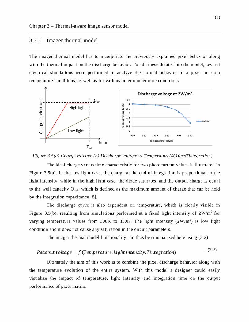
68
Chapter 3 – Thermal-aware image sensor model
3.3.2 Imager thermal model
The imager thermal model has to incorporate the previously explained pixel behavior along
with the thermal impact on the discharge behavior. To add these details into the model, several
electrical simulations were performed to analyze the normal behavior of a pixel in room
temperature conditions, as well as for various other temperature conditions.
The ideal charge versus time characteristic for two photocurrent values is illustrated in
Figure 3.5(a). In the low light case, the charge at the end of integration is proportional to the
light intensity, while in the high light case, the diode saturates, and the output charge is equal
to the well capacity Qsat
The discharge curve is also dependent on temperature, which is clearly visible in
, which is defined as the maximum amount of charge that can be held
by the integration capacitance [8].
Figure 3.5(b), resulting from simulations performed at a fixed light intensity of 2W/m2 for
varying temperature values from 300K to 350K. The light intensity (2W/m2
𝑅𝑅𝑅𝑅𝑅𝑅𝑅𝑅𝑅𝑅𝑅𝑅𝑅𝑅 𝑣𝑣𝑅𝑅𝑣𝑣𝑅𝑅𝑅𝑅𝑣𝑣𝑅𝑅 = 𝑓𝑓 (𝑇𝑇𝑅𝑅𝑇𝑇𝑇𝑇𝑅𝑅𝑇𝑇𝑅𝑅𝑅𝑅𝑅𝑅𝑇𝑇𝑅𝑅, 𝐿𝐿𝐿𝐿𝑣𝑣ℎ𝑅𝑅 𝐿𝐿𝑛𝑛𝑅𝑅𝑅𝑅𝑛𝑛𝑖𝑖𝐿𝐿𝑅𝑅𝑖𝑖,𝑇𝑇𝐿𝐿𝑛𝑛𝑅𝑅𝑅𝑅𝑣𝑣𝑇𝑇𝑅𝑅𝑅𝑅𝐿𝐿𝑅𝑅𝑛𝑛)
) is low light
condition and it does not cause any saturation in the circuit parameters.
The imager thermal model functionality can thus be summarized here using (3.2)
--(3.2)
Ultimately the aim of this work is to combine the pixel discharge behavior along with
the temperature evolution of the entire system. With this model a designer could easily
visualize the impact of temperature, light intensity and integration time on the output
performance of pixel matrix.
Tint
Time
Char
ge (i
n el
ectr
ons) Qsat
Low light
High light
Figure 3.5(a) Charge vs Time (b) Discharge voltage vs Temperature(@10msTintegration)
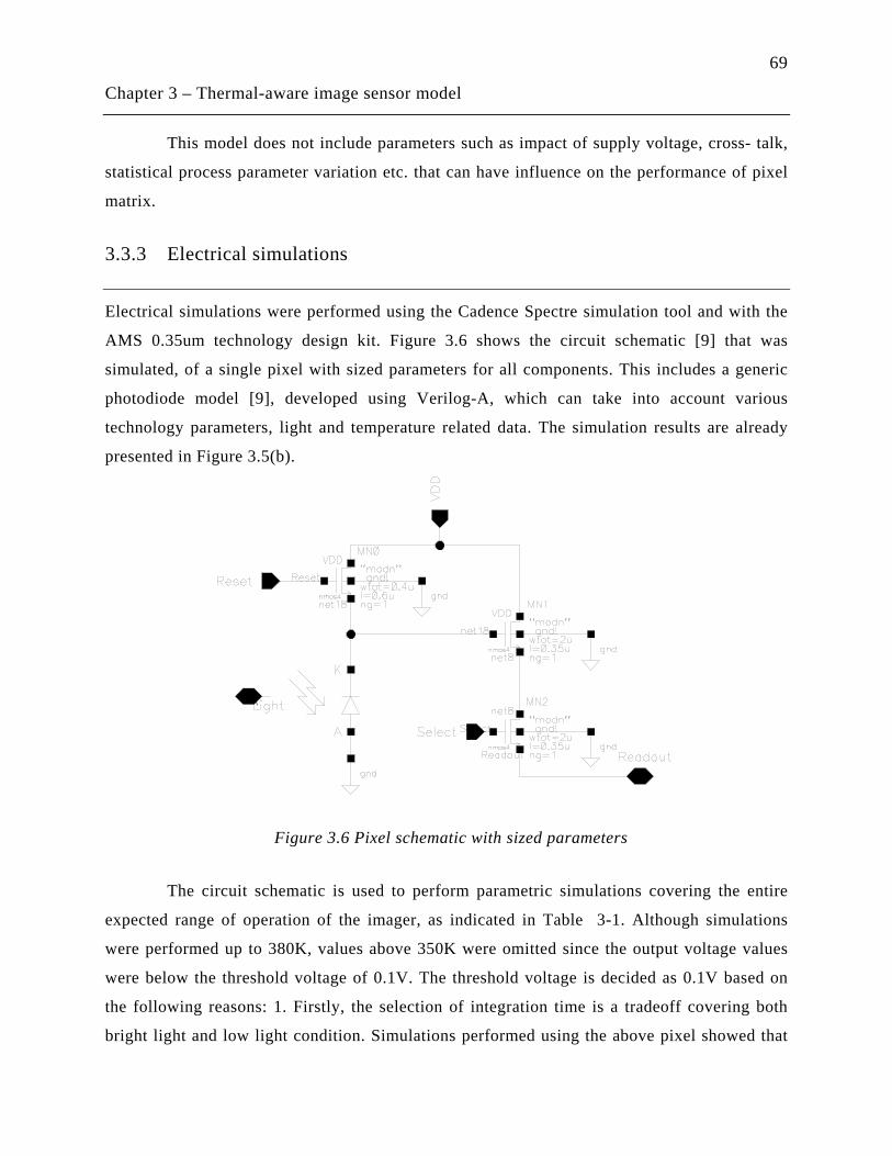
69
Chapter 3 – Thermal-aware image sensor model
This model does not include parameters such as impact of supply voltage, cross- talk,
statistical process parameter variation etc. that can have influence on the performance of pixel
matrix.
3.3.3 Electrical simulations
Electrical simulations were performed using the Cadence Spectre simulation tool and with the
AMS 0.35um technology design kit. Figure 3.6 shows the circuit schematic [9] that was
simulated, of a single pixel with sized parameters for all components. This includes a generic
photodiode model [9], developed using Verilog-A, which can take into account various
technology parameters, light and temperature related data. The simulation results are already
presented in Figure 3.5(b).
The circuit schematic is used to perform parametric simulations covering the entire
expected range of operation of the imager, as indicated in Table 3-1. Although simulations
were performed up to 380K, values above 350K were omitted since the output voltage values
were below the threshold voltage of 0.1V. The threshold voltage is decided as 0.1V based on
the following reasons: 1. Firstly, the selection of integration time is a tradeoff covering both
bright light and low light condition. Simulations performed using the above pixel showed that
Figure 3.6 Pixel schematic with sized parameters
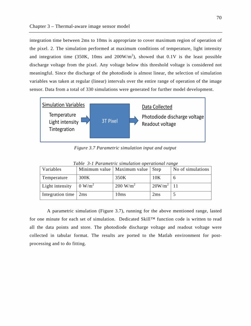
70
Chapter 3 – Thermal-aware image sensor model
integration time between 2ms to 10ms is appropriate to cover maximum region of operation of
the pixel. 2. The simulation performed at maximum conditions of temperature, light intensity
and integration time (350K, 10ms and 200W/m2
), showed that 0.1V is the least possible
discharge voltage from the pixel. Any voltage below this threshold voltage is considered not
meaningful. Since the discharge of the photodiode is almost linear, the selection of simulation
variables was taken at regular (linear) intervals over the entire range of operation of the image
sensor. Data from a total of 330 simulations were generated for further model development.
Table 3-1 Parametric simulation operational range Variables Minimum value Maximum value Step No of simulations
Temperature 300K 350K 10K 6
Light intensity 0 W/m 200 W/m2 20W/m2 11 2
Integration time 2ms 10ms 2ms 5
A parametric simulation (Figure 3.7), running for the above mentioned range, lasted
for one minute for each set of simulation. Dedicated Skill™ function code is written to read
all the data points and store. The photodiode discharge voltage and readout voltage were
collected in tabular format. The results are ported to the Matlab environment for post-
processing and to do fitting.
3T PixelTemperatureLight intensityTintegration
Simulation Variables Data Collected
Photodiode discharge voltageReadout voltage
Figure 3.7 Parametric simulation input and output
71
Chapter 3 – Thermal-aware image sensor model
3.4 Fitting
3.4.1 Types of fitting
Fitting is a process of constructing a curve or mathematical function that fits the series of data
points. We have performed various simulations and collected the series of data points which
exhibits the behavior of pixel. The aim of the fitting is to find a mathematical function that fits
well with the data points. The well known types of fitting are
• Least Squares fitting
• Non linear fitting
• Smoothing fitting
Least Squares is the most popular method of fitting. It is relatively simple in terms of
required computing power. Least Squares minimizes the square of the error between the
original data and the values predicted by the equation. Least Squares method is sensitivity to
outliers in the data. If a data point is widely different from the majority of the data, it can skew
the results of the regression. So it is important to examine the data before fitting. The most
well known types of Least squares fitting are linear, polynomial, exponential and logarithmic.
As the name suggests linear least square fitting uses a function to fit a straight line through the
data. Polynomial function fits a curve through the data. Higher order polynomial can be used
if the curve needs a complex curvature. Exponential function is used if the data increases or
decreases at high rate. Logarithmic is used if the data that spans in decades. Exponential and
Logarithmic cannot be used if the data spans through negative or zero values.
The non linear fitting is a method that provides a numerical solution for a problem of
minimizing function which are non linear. This method starts with an initial guess of an
unknown parameter that calculates a value which represents the sum of squared error between
data and the calculated fit.
Smoothing fitting, as the name suggests is used to improve the appearance of plot by
drawing a smooth curve through the data. This fitting generally does not generate any equation
for the resulting curve. This is because there is no single equation that can be used to represent
the curve. Commonly known smooth fitting methodologies are Smooth, Weighted, Cubic
Spline and Interpolate. Smooth and Interpolate uses a geometric weight to arrive to a final
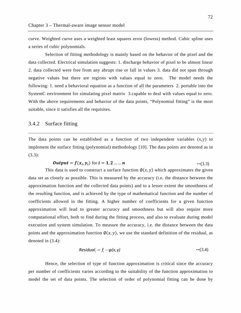
72
Chapter 3 – Thermal-aware image sensor model
curve. Weighted curve uses a weighted least squares error (lowess) method. Cubic spline uses
a series of cubic polynomials.
Selection of fitting methodology is mainly based on the behavior of the pixel and the
data collected. Electrical simulation suggests: 1. discharge behavior of pixel to be almost linear
2. data collected were free from any abrupt rise or fall in values 3. data did not span through
negative values but there are regions with values equal to zero. The model needs the
following: 1. need a behavioral equation as a function of all the parameters 2. portable into the
SystemC environment for simulating pixel matrix 3.capable to deal with values equal to zero.
With the above requirements and behavior of the data points, “Polynomial fitting” is the most
suitable, since it satisfies all the requisites.
3.4.2 Surface fitting
The data points can be established as a function of two independent variables (x,y) to
implement the surface fitting (polynomial) methodology [10]. The data points are denoted as in
(3.3):
𝑶𝑶𝑶𝑶𝑶𝑶𝑶𝑶𝑶𝑶𝑶𝑶 = 𝒇𝒇(𝒙𝒙𝒊𝒊,𝒚𝒚𝒊𝒊) for 𝒊𝒊 = 𝟏𝟏,𝟐𝟐… …𝒏𝒏
--(3.3) This data is used to construct a surface function ∅(𝑥𝑥,𝑖𝑖) which approximates the given
data set as closely as possible. This is measured by the accuracy (i.e. the distance between the
approximation function and the collected data points) and to a lesser extent the smoothness of
the resulting function, and is achieved by the type of mathematical function and the number of
coefficients allowed in the fitting. A higher number of coefficients for a given function
approximation will lead to greater accuracy and smoothness but will also require more
computational effort, both to find during the fitting process, and also to evaluate during model
execution and system simulation. To measure the accuracy, i.e. the distance between the data
points and the approximation function ∅(𝑥𝑥, 𝑖𝑖), we use the standard definition of the residual, as
denoted in (3.4):
--(3.4)
Hence, the selection of type of function approximation is critical since the accuracy
per number of coefficients varies according to the suitability of the function approximation to
model the set of data points. The selection of order of polynomial fitting can be done by
y)φ(x,fResidual ii −=

73
Chapter 3 – Thermal-aware image sensor model
comparing the number of coefficients and different surface fitted results. When the order is low
the fitting will be poor and if the order is high the fitting will be as close as possible. However,
we can already indicate that we use polynomial fitting in the current problem because the
performance space represented by z does not have any sharp peaks or sudden change in
behavior, and we should therefore use a continuous mathematical function. We also consider
that the set of data points with which we are dealing extends to the entire range of operation of
the system. In other words, the system is not expected to operate (and it is not expected to
simulate the model) outside this range, so the fitting range is bounded. The robustness of this
methodology will be proved by checking the fitting at number of intermediate points (i.e.
points which have been evaluated at electrical but which have not been used in the fitting
process).
As a starting point to prove the methodology, we formulated the problem with only
two independent variables (temperature, light intensity) as expanded in (3.5)
--(3.5)
Parametric simulations were performed to collect the photodiode discharge voltage
and readout voltage for the above function at a fixed integration time value (10ms). This value
is chosen to check the model capability at the end of system operating range (350K, 200W/m2
Figure 3.8
and 10ms). Moreover, this is just an indicative value chosen to prove the surface fitting
methodology and proceed with developing a model with all the three variables to cover the
entire system range. shows the fitting obtained for a fifth order function in terms
of temperature and light intensity as indicated in equation (3.6).
--(3.6) ( )
∧
=
55
00
sityLightinteneTemperatur*Coeff
CoefftageReadoutvol
m
1
)sityLightinten,uref(TemperattageReadoutvol iii =
74
Chapter 3 – Thermal-aware image sensor model
.
The complete equation used in solving this problem, coefficient values and goodness
of fit values along with the residual plot are given in Appendix I.
Having established the basic methodology for two independent variables, we must
now deal with three variables and extend the approach to the entire range of pixel operation.
3.4.3 Volume fitting
In this section we will discuss in detail about including another independent variable in the
surface fitting [10] methodology. Integration time is the third independent variable which is
dealt along with temperature and light intensity. The photodiode discharge voltage or readout
voltage dependence is expressed in (3.7):
--(3.7)
We have used readout voltage in most of the work, since we are more interested in the
output voltage of the pixel. Nevertheless, the model is capable of providing the photodiode
voltage as well as illustrated in Figure 3.9. The model has the capability to use of any order of
polynomial to. We have restricted the orders of fitting from third to sixth order for the
following reasons: 1. below the third order the fitting error is high in comparison to electrical
simulation results 2. At the sixth order the accuracy was as expected in terms of quanta 3.
Increasing the order than required will result in simulation time. These points are explained in
the following sections.
Figure 3.8 Surface fitting with two variables
)onTintegrati ,sityLightinten,uref(TemperattageReadoutvol iiii =
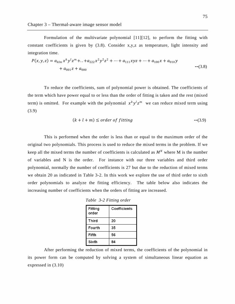
75
Chapter 3 – Thermal-aware image sensor model
Formulation of the multivariate polynomial [11][12], to perform the fitting with
constant coefficients is given by (3.8). Consider x,y,z as temperature, light intensity and
integration time.
𝑃𝑃(𝑥𝑥,𝑖𝑖, 𝑧𝑧) = 𝑅𝑅𝑘𝑘𝑣𝑣𝑇𝑇 𝑥𝑥𝑘𝑘𝑖𝑖𝑣𝑣𝑧𝑧𝑇𝑇+. . +𝑅𝑅222𝑥𝑥2𝑖𝑖2𝑧𝑧2 + ⋯+ 𝑅𝑅111𝑥𝑥𝑖𝑖𝑧𝑧 + ⋯+ 𝑅𝑅100𝑥𝑥 + 𝑅𝑅010𝑖𝑖
+ 𝑅𝑅001𝑧𝑧 + 𝑅𝑅000
--(3.8)
To reduce the coefficients, sum of polynomial power is obtained. The coefficients of
the term which have power equal to or less than the order of fitting is taken and the rest (mixed
term) is omitted. For example with the polynomial 𝑥𝑥𝑘𝑘𝑖𝑖𝑣𝑣𝑧𝑧𝑇𝑇 we can reduce mixed term using
(3.9)
(𝑘𝑘 + 𝑣𝑣 + 𝑇𝑇) ≤ 𝑅𝑅𝑇𝑇𝑅𝑅𝑅𝑅𝑇𝑇 𝑅𝑅𝑓𝑓 𝑓𝑓𝐿𝐿𝑅𝑅𝑅𝑅𝐿𝐿𝑛𝑛𝑣𝑣 --(3.9)
This is performed when the order is less than or equal to the maximum order of the
original two polynomials. This process is used to reduce the mixed terms in the problem. If we
keep all the mixed terms the number of coefficients is calculated as 𝑀𝑀𝑁𝑁 where M is the number
of variables and N is the order. For instance with our three variables and third order
polynomial, normally the number of coefficients is 27 but due to the reduction of mixed terms
we obtain 20 as indicated in Table 3-2. In this work we explore the use of third order to sixth
order polynomials to analyze the fitting efficiency. The table below also indicates the
increasing number of coefficients when the orders of fitting are increased.
After performing the reduction of mixed terms, the coefficients of the polynomial in
its power form can be computed by solving a system of simultaneous linear equation as
expressed in (3.10)
Table 3-2 Fitting order
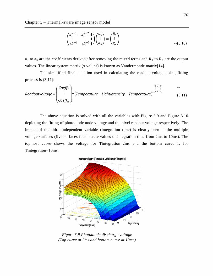
76
Chapter 3 – Thermal-aware image sensor model
𝑥𝑥1𝑛𝑛−1 𝑥𝑥1
𝑛𝑛−2
⋮ ⋮𝑥𝑥𝑛𝑛𝑛𝑛−1 𝑥𝑥𝑛𝑛𝑛𝑛−2
111
𝑅𝑅1⋮𝑅𝑅𝑛𝑛 =
𝑅𝑅1⋮𝑅𝑅𝑛𝑛
--(3.10)
a1 to an are the coefficients derived after removing the mixed terms and R1 to Rn
are the output
values. The linear system matrix (x values) is known as Vandermonde matrix[14].
The simplified final equation used in calculating the readout voltage using fitting
process is (3.11):
--(3.11)
The above equation is solved with all the variables with Figure 3.9 and Figure 3.10
depicting the fitting of photodiode node voltage and the pixel readout voltage respectively. The
impact of the third independent variable (integration time) is clearly seen in the multiple
voltage surfaces (five surfaces for discrete values of integration time from 2ms to 10ms). The
topmost curve shows the voltage for Tintegration=2ms and the bottom curve is for
Tintegration=10ms.
Figure 3.9 Photodiode discharge voltage (Top curve at 2ms and bottom curve at 10ms)
( )
∧
=
666
000
eTemperatursityLightinteneTemperatur*Coeff
CoefftageReadoutvol
m
1
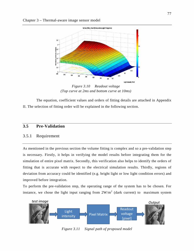
77
Chapter 3 – Thermal-aware image sensor model
The equation, coefficient values and orders of fitting details are attached in Appendix
II. The selection of fitting order will be explained in the following section.
3.5 Pre-Validation
3.5.1 Requirement
As mentioned in the previous section the volume fitting is complex and so a pre-validation step
is necessary. Firstly, it helps in verifying the model results before integrating them for the
simulation of entire pixel matrix. Secondly, this verification also helps to identify the orders of
fitting that is accurate with respect to the electrical simulation results. Thirdly, regions of
deviation from accuracy could be identified (e.g. bright light or low light condition errors) and
improved before integration.
To perform the pre-validation step, the operating range of the system has to be chosen. For
instance, we chose the light input ranging from 2W/m2 (dark current) to maximum system
test image
Light intensity Pixel Matrix
Readout voltage[pixel]
Output
Figure 3.10 Readout voltage (Top curve at 2ms and bottom curve at 10ms)
Figure 3.11 Signal path of proposed model
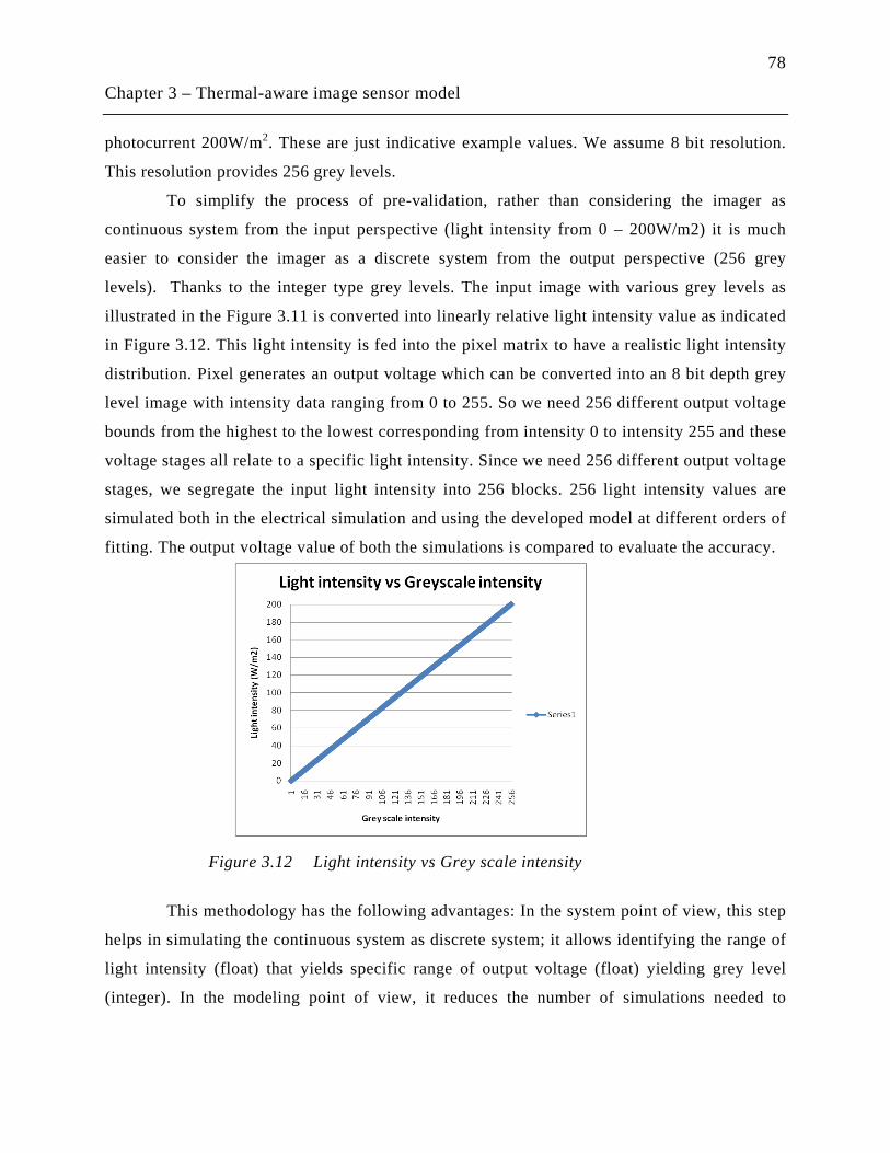
78
Chapter 3 – Thermal-aware image sensor model
photocurrent 200W/m2
To simplify the process of pre-validation, rather than considering the imager as
continuous system from the input perspective (light intensity from 0 – 200W/m2) it is much
easier to consider the imager as a discrete system from the output perspective (256 grey
levels). Thanks to the integer type grey levels. The input image with various grey levels as
illustrated in the
. These are just indicative example values. We assume 8 bit resolution.
This resolution provides 256 grey levels.
Figure 3.11 is converted into linearly relative light intensity value as indicated
in Figure 3.12. This light intensity is fed into the pixel matrix to have a realistic light intensity
distribution. Pixel generates an output voltage which can be converted into an 8 bit depth grey
level image with intensity data ranging from 0 to 255. So we need 256 different output voltage
bounds from the highest to the lowest corresponding from intensity 0 to intensity 255 and these
voltage stages all relate to a specific light intensity. Since we need 256 different output voltage
stages, we segregate the input light intensity into 256 blocks. 256 light intensity values are
simulated both in the electrical simulation and using the developed model at different orders of
fitting. The output voltage value of both the simulations is compared to evaluate the accuracy.
This methodology has the following advantages: In the system point of view, this step
helps in simulating the continuous system as discrete system; it allows identifying the range of
light intensity (float) that yields specific range of output voltage (float) yielding grey level
(integer). In the modeling point of view, it reduces the number of simulations needed to
Figure 3.12 Light intensity vs Grey scale intensity
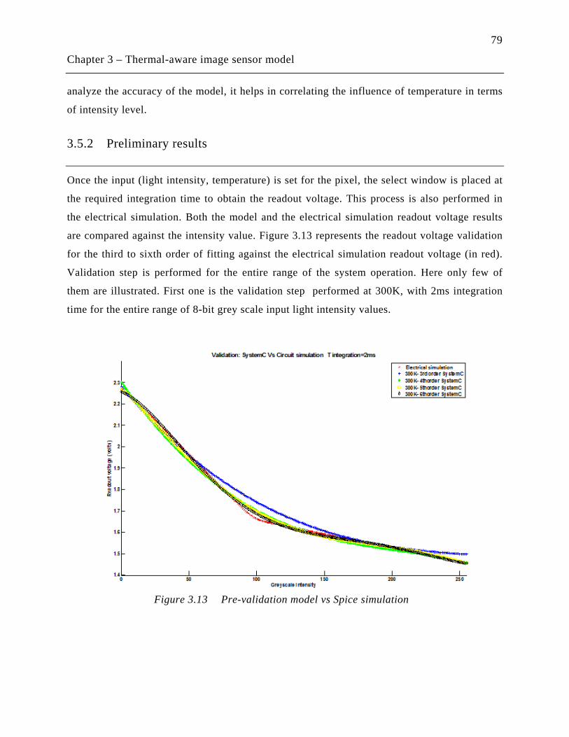
79
Chapter 3 – Thermal-aware image sensor model
analyze the accuracy of the model, it helps in correlating the influence of temperature in terms
of intensity level.
3.5.2 Preliminary results
Once the input (light intensity, temperature) is set for the pixel, the select window is placed at
the required integration time to obtain the readout voltage. This process is also performed in
the electrical simulation. Both the model and the electrical simulation readout voltage results
are compared against the intensity value. Figure 3.13 represents the readout voltage validation
for the third to sixth order of fitting against the electrical simulation readout voltage (in red).
Validation step is performed for the entire range of the system operation. Here only few of
them are illustrated. First one is the validation step performed at 300K, with 2ms integration
time for the entire range of 8-bit grey scale input light intensity values.
Figure 3.13 Pre-validation model vs Spice simulation
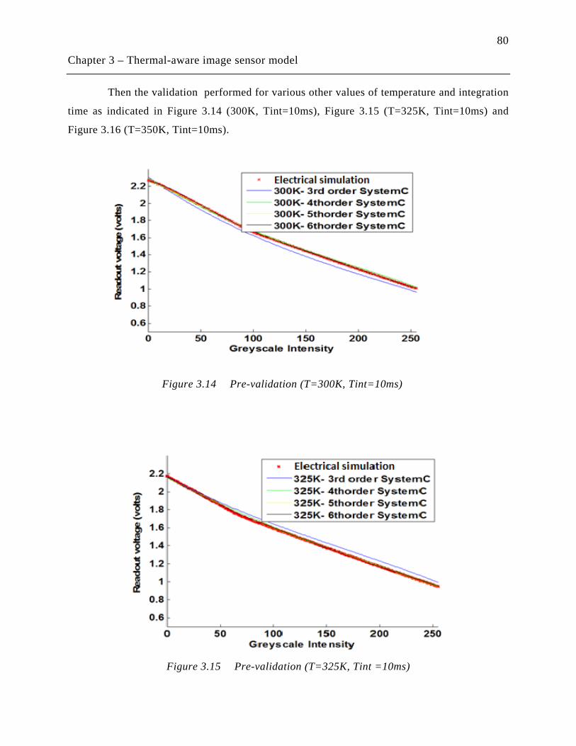
80
Chapter 3 – Thermal-aware image sensor model
Then the validation performed for various other values of temperature and integration
time as indicated in Figure 3.14 (300K, Tint=10ms), Figure 3.15 (T=325K, Tint=10ms) and
Figure 3.16 (T=350K, Tint=10ms).
Figure 3.15 Pre-validation (T=325K, Tint =10ms)
Figure 3.14 Pre-validation (T=300K, Tint=10ms)
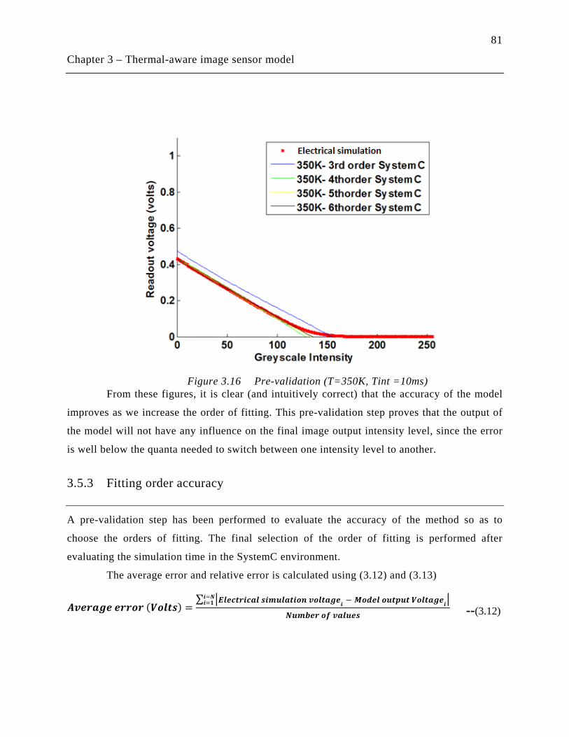
81
Chapter 3 – Thermal-aware image sensor model
From these figures, it is clear (and intuitively correct) that the accuracy of the model
improves as we increase the order of fitting. This pre-validation step proves that the output of
the model will not have any influence on the final image output intensity level, since the error
is well below the quanta needed to switch between one intensity level to another.
3.5.3 Fitting order accuracy
A pre-validation step has been performed to evaluate the accuracy of the method so as to
choose the orders of fitting. The final selection of the order of fitting is performed after
evaluating the simulation time in the SystemC environment.
The average error and relative error is calculated using (3.12) and (3.13)
𝑨𝑨𝑨𝑨𝑨𝑨𝑨𝑨𝑨𝑨𝑨𝑨𝑨𝑨 𝑨𝑨𝑨𝑨𝑨𝑨𝒆𝒆𝑨𝑨 (𝑽𝑽𝒆𝒆𝑽𝑽𝑶𝑶𝑽𝑽) =∑ 𝑬𝑬𝑽𝑽𝑨𝑨𝑬𝑬𝑶𝑶𝑨𝑨𝒊𝒊𝑬𝑬𝑨𝑨𝑽𝑽 𝑽𝑽𝒊𝒊𝒔𝒔𝑶𝑶𝑽𝑽𝑨𝑨𝑶𝑶𝒊𝒊𝒆𝒆𝒏𝒏 𝑨𝑨𝒆𝒆𝑽𝑽𝑶𝑶𝑨𝑨𝑨𝑨𝑨𝑨𝒊𝒊 − 𝑴𝑴𝒆𝒆𝑴𝑴𝑨𝑨𝑽𝑽 𝒆𝒆𝑶𝑶𝑶𝑶𝑶𝑶𝑶𝑶𝑶𝑶 𝑽𝑽𝒆𝒆𝑽𝑽𝑶𝑶𝑨𝑨𝑨𝑨𝑨𝑨𝒊𝒊
𝒊𝒊=𝑵𝑵𝒊𝒊=𝟏𝟏
𝑵𝑵𝑶𝑶𝒔𝒔𝒎𝒎𝑨𝑨𝑨𝑨 𝒆𝒆𝒇𝒇 𝑨𝑨𝑨𝑨𝑽𝑽𝑶𝑶𝑨𝑨𝑽𝑽 --(3.12)
Figure 3.16 Pre-validation (T=350K, Tint =10ms)
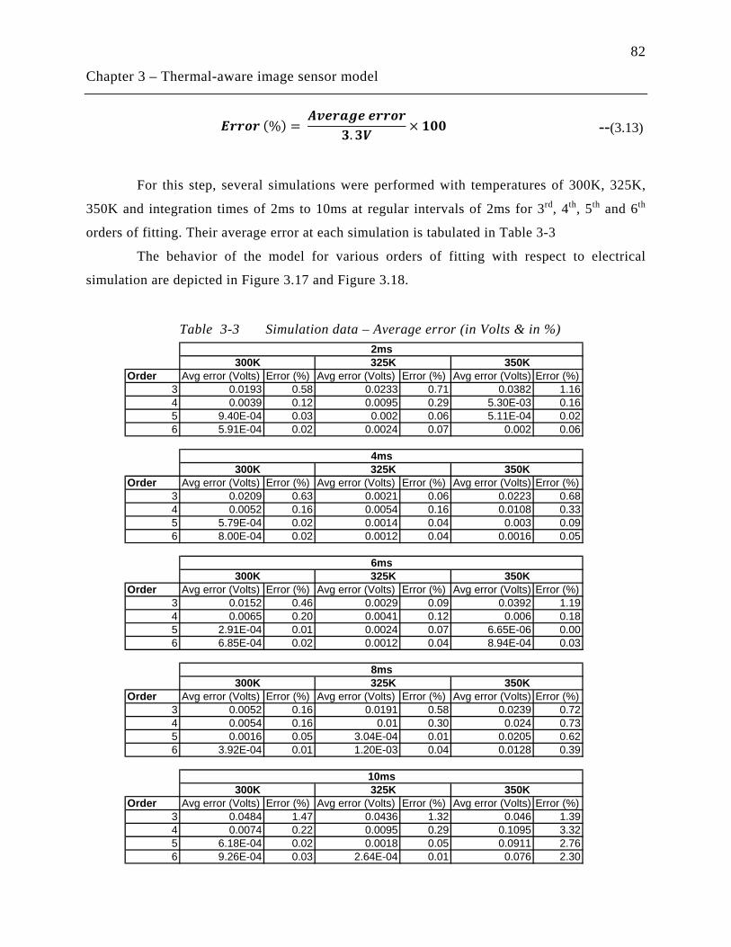
82
Chapter 3 – Thermal-aware image sensor model
𝑬𝑬𝑨𝑨𝑨𝑨𝒆𝒆𝑨𝑨 (%) = 𝑨𝑨𝑨𝑨𝑨𝑨𝑨𝑨𝑨𝑨𝑨𝑨𝑨𝑨 𝑨𝑨𝑨𝑨𝑨𝑨𝒆𝒆𝑨𝑨
𝟑𝟑.𝟑𝟑𝑽𝑽 × 𝟏𝟏𝟏𝟏𝟏𝟏 --(3.13)
For this step, several simulations were performed with temperatures of 300K, 325K,
350K and integration times of 2ms to 10ms at regular intervals of 2ms for 3rd, 4th, 5th and 6th
The behavior of the model for various orders of fitting with respect to electrical
simulation are depicted in
orders of fitting. Their average error at each simulation is tabulated in Table 3-3
Figure 3.17 and Figure 3.18.
Order Avg error (Volts) Error (%) Avg error (Volts) Error (%) Avg error (Volts) Error (%)3 0.0193 0.58 0.0233 0.71 0.0382 1.164 0.0039 0.12 0.0095 0.29 5.30E-03 0.165 9.40E-04 0.03 0.002 0.06 5.11E-04 0.026 5.91E-04 0.02 0.0024 0.07 0.002 0.06
Order Avg error (Volts) Error (%) Avg error (Volts) Error (%) Avg error (Volts) Error (%)3 0.0209 0.63 0.0021 0.06 0.0223 0.684 0.0052 0.16 0.0054 0.16 0.0108 0.335 5.79E-04 0.02 0.0014 0.04 0.003 0.096 8.00E-04 0.02 0.0012 0.04 0.0016 0.05
Order Avg error (Volts) Error (%) Avg error (Volts) Error (%) Avg error (Volts) Error (%)3 0.0152 0.46 0.0029 0.09 0.0392 1.194 0.0065 0.20 0.0041 0.12 0.006 0.185 2.91E-04 0.01 0.0024 0.07 6.65E-06 0.006 6.85E-04 0.02 0.0012 0.04 8.94E-04 0.03
Order Avg error (Volts) Error (%) Avg error (Volts) Error (%) Avg error (Volts) Error (%)3 0.0052 0.16 0.0191 0.58 0.0239 0.724 0.0054 0.16 0.01 0.30 0.024 0.735 0.0016 0.05 3.04E-04 0.01 0.0205 0.626 3.92E-04 0.01 1.20E-03 0.04 0.0128 0.39
Order Avg error (Volts) Error (%) Avg error (Volts) Error (%) Avg error (Volts) Error (%)3 0.0484 1.47 0.0436 1.32 0.046 1.394 0.0074 0.22 0.0095 0.29 0.1095 3.325 6.18E-04 0.02 0.0018 0.05 0.0911 2.766 9.26E-04 0.03 2.64E-04 0.01 0.076 2.30
300K 325K 350K10ms
300K 325K 350K
300K 325K 350K8ms
4ms300K 325K 350K
6ms
2ms300K 325K 350K
Table 3-3 Simulation data – Average error (in Volts & in %)
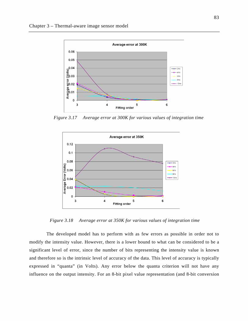
83
Chapter 3 – Thermal-aware image sensor model
The developed model has to perform with as few errors as possible in order not to
modify the intensity value. However, there is a lower bound to what can be considered to be a
significant level of error, since the number of bits representing the intensity value is known
and therefore so is the intrinsic level of accuracy of the data. This level of accuracy is typically
expressed in “quanta” (in Volts). Any error below the quanta criterion will not have any
influence on the output intensity. For an 8-bit pixel value representation (and 8-bit conversion
Figure 3.17 Average error at 300K for various values of integration time
Figure 3.18 Average error at 350K for various values of integration time
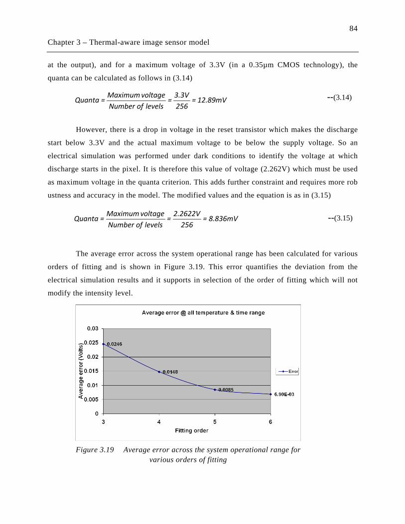
84
Chapter 3 – Thermal-aware image sensor model
at the output), and for a maximum voltage of 3.3V (in a 0.35µm CMOS technology), the
quanta can be calculated as follows in (3.14)
--(3.14)
However, there is a drop in voltage in the reset transistor which makes the discharge
start below 3.3V and the actual maximum voltage to be below the supply voltage. So an
electrical simulation was performed under dark conditions to identify the voltage at which
discharge starts in the pixel. It is therefore this value of voltage (2.262V) which must be used
as maximum voltage in the quanta criterion. This adds further constraint and requires more rob
ustness and accuracy in the model. The modified values and the equation is as in (3.15)
--(3.15)
The average error across the system operational range has been calculated for various
orders of fitting and is shown in Figure 3.19. This error quantifies the deviation from the
electrical simulation results and it supports in selection of the order of fitting which will not
modify the intensity level.
12.89mV=2563.3V=
levels of Numbervoltage Maximum=Quanta
8.836mV=256
2.2622V=levels of Number
voltage Maximum=Quanta
Figure 3.19 Average error across the system operational range for various orders of fitting
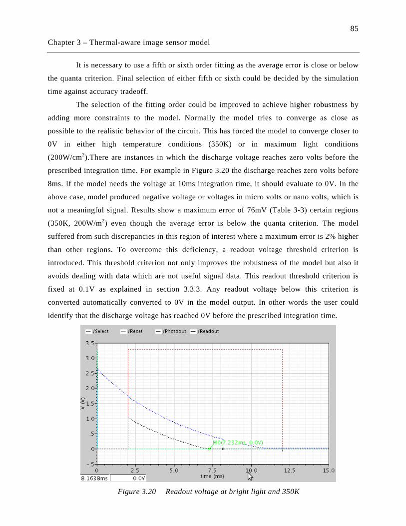
85
Chapter 3 – Thermal-aware image sensor model
It is necessary to use a fifth or sixth order fitting as the average error is close or below
the quanta criterion. Final selection of either fifth or sixth could be decided by the simulation
time against accuracy tradeoff.
The selection of the fitting order could be improved to achieve higher robustness by
adding more constraints to the model. Normally the model tries to converge as close as
possible to the realistic behavior of the circuit. This has forced the model to converge closer to
0V in either high temperature conditions (350K) or in maximum light conditions
(200W/cm2
Figure 3.20
).There are instances in which the discharge voltage reaches zero volts before the
prescribed integration time. For example in the discharge reaches zero volts before
8ms. If the model needs the voltage at 10ms integration time, it should evaluate to 0V. In the
above case, model produced negative voltage or voltages in micro volts or nano volts, which is
not a meaningful signal. Results show a maximum error of 76mV (Table 3-3) certain regions
(350K, 200W/m2) even though the average error is below the quanta criterion. The model
suffered from such discrepancies in this region of interest where a maximum error is 2% higher
than other regions. To overcome this deficiency, a readout voltage threshold criterion is
introduced. This threshold criterion not only improves the robustness of the model but also it
avoids dealing with data which are not useful signal data. This readout threshold criterion is
fixed at 0.1V as explained in section 3.3.3. Any readout voltage below this criterion is
converted automatically converted to 0V in the model output. In other words the user could
identify that the discharge voltage has reached 0V before the prescribed integration time.
Figure 3.20 Readout voltage at bright light and 350K
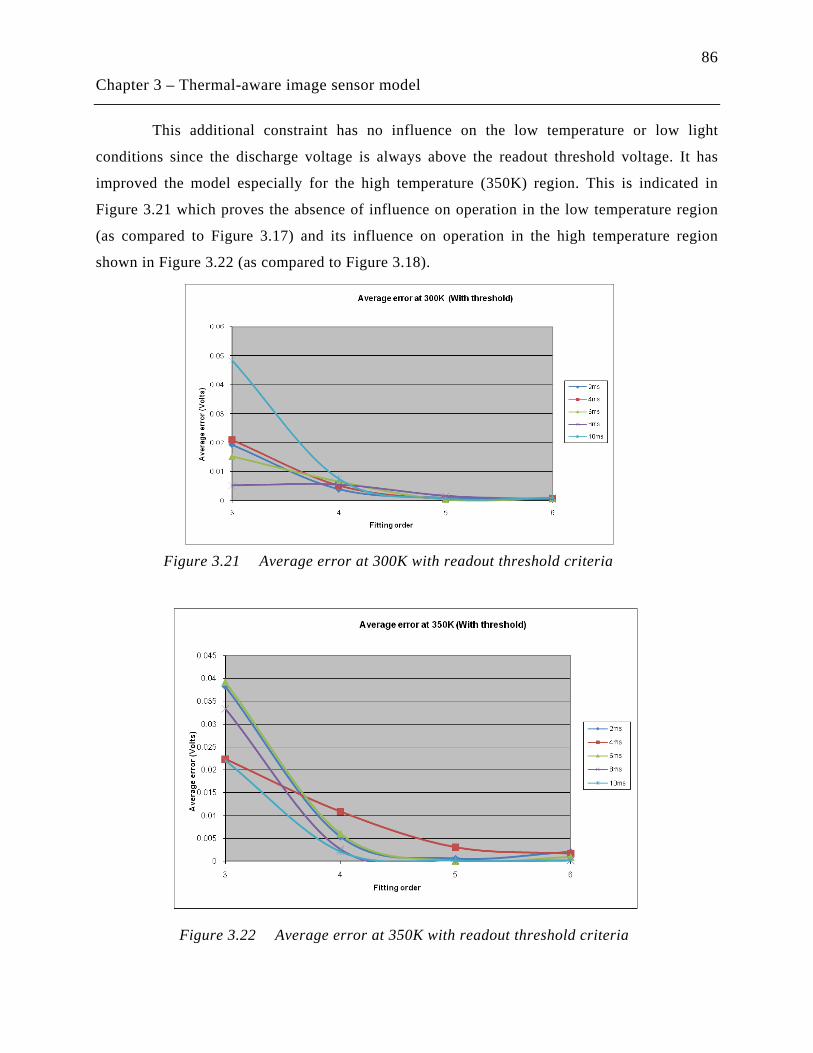
86
Chapter 3 – Thermal-aware image sensor model
This additional constraint has no influence on the low temperature or low light
conditions since the discharge voltage is always above the readout threshold voltage. It has
improved the model especially for the high temperature (350K) region. This is indicated in
Figure 3.21 which proves the absence of influence on operation in the low temperature region
(as compared to Figure 3.17) and its influence on operation in the high temperature region
shown in Figure 3.22 (as compared to Figure 3.18).
Figure 3.21 Average error at 300K with readout threshold criteria
Figure 3.22 Average error at 350K with readout threshold criteria
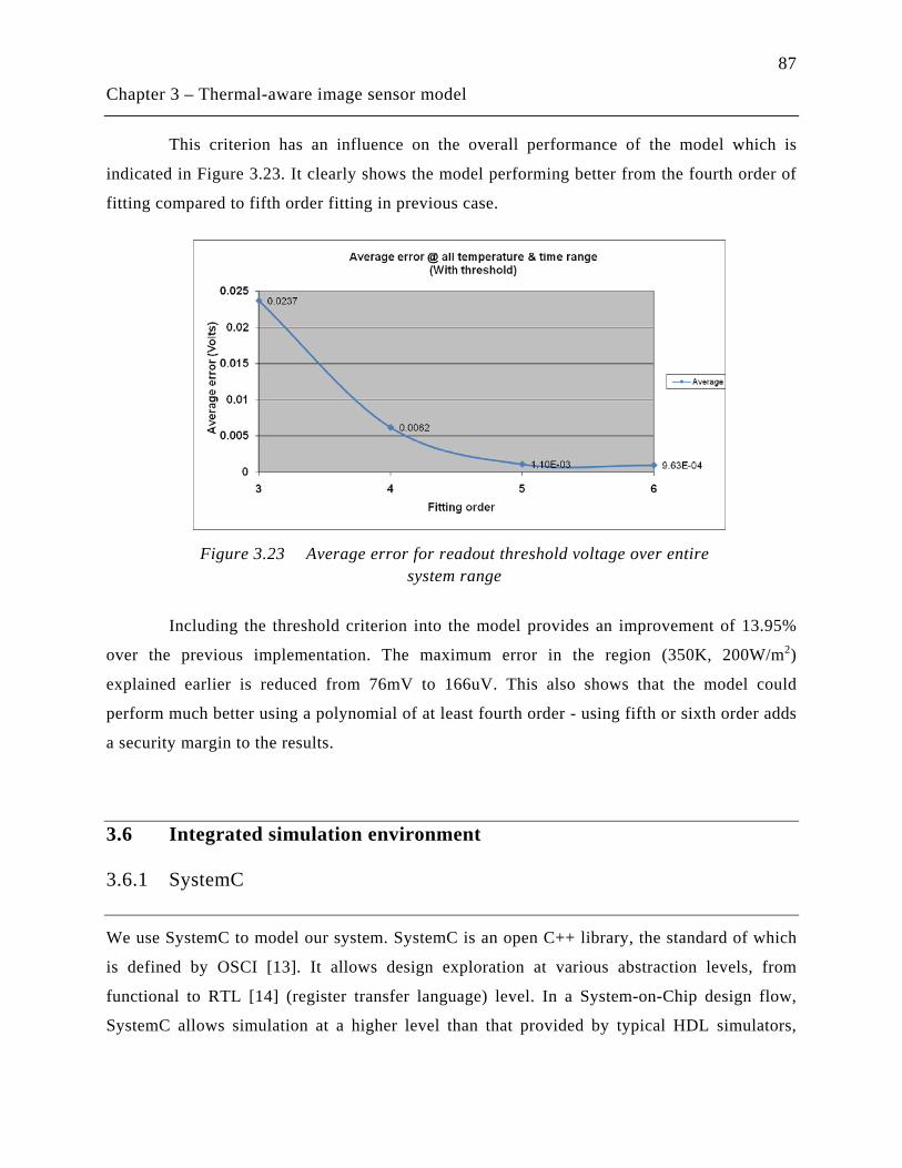
87
Chapter 3 – Thermal-aware image sensor model
This criterion has an influence on the overall performance of the model which is
indicated in Figure 3.23. It clearly shows the model performing better from the fourth order of
fitting compared to fifth order fitting in previous case.
Including the threshold criterion into the model provides an improvement of 13.95%
over the previous implementation. The maximum error in the region (350K, 200W/m2
3.6 Integrated simulation environment
)
explained earlier is reduced from 76mV to 166uV. This also shows that the model could
perform much better using a polynomial of at least fourth order - using fifth or sixth order adds
a security margin to the results.
3.6.1 SystemC
We use SystemC to model our system. SystemC is an open C++ library, the standard of which
is defined by OSCI [13]. It allows design exploration at various abstraction levels, from
functional to RTL [14] (register transfer language) level. In a System-on-Chip design flow,
SystemC allows simulation at a higher level than that provided by typical HDL simulators,
Figure 3.23 Average error for readout threshold voltage over entire system range
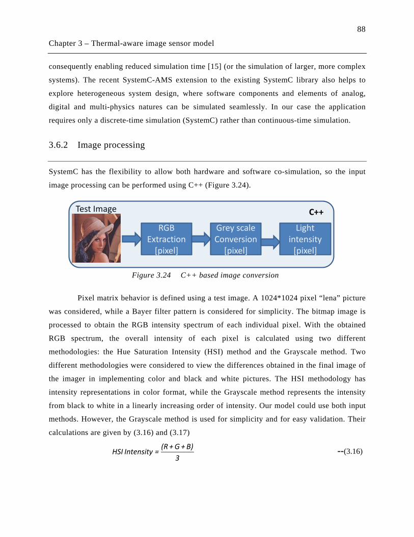
88
Chapter 3 – Thermal-aware image sensor model
consequently enabling reduced simulation time [15] (or the simulation of larger, more complex
systems). The recent SystemC-AMS extension to the existing SystemC library also helps to
explore heterogeneous system design, where software components and elements of analog,
digital and multi-physics natures can be simulated seamlessly. In our case the application
requires only a discrete-time simulation (SystemC) rather than continuous-time simulation.
3.6.2 Image processing
SystemC has the flexibility to allow both hardware and software co-simulation, so the input
image processing can be performed using C++ (Figure 3.24).
Pixel matrix behavior is defined using a test image. A 1024*1024 pixel “lena” picture
was considered, while a Bayer filter pattern is considered for simplicity. The bitmap image is
processed to obtain the RGB intensity spectrum of each individual pixel. With the obtained
RGB spectrum, the overall intensity of each pixel is calculated using two different
methodologies: the Hue Saturation Intensity (HSI) method and the Grayscale method. Two
different methodologies were considered to view the differences obtained in the final image of
the imager in implementing color and black and white pictures. The HSI methodology has
intensity representations in color format, while the Grayscale method represents the intensity
from black to white in a linearly increasing order of intensity. Our model could use both input
methods. However, the Grayscale method is used for simplicity and for easy validation. Their
calculations are given by (3.16) and (3.17)
--(3.16)
RGB Extraction
[pixel]
Grey scaleConversion
[pixel]
Light intensity
[pixel]
Test Image C++
Figure 3.24 C++ based image conversion
3B)+G+(R=IntensityHSI
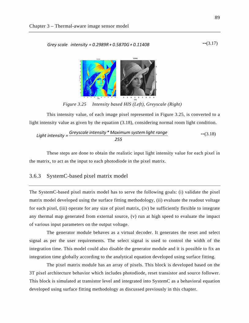
89
Chapter 3 – Thermal-aware image sensor model
--(3.17)
This intensity value, of each image pixel represented in Figure 3.25, is converted to a
light intensity value as given by the equation (3.18), considering normal room light condition.
--(3.18)
These steps are done to obtain the realistic input light intensity value for each pixel in
the matrix, to act as the input to each photodiode in the pixel matrix.
3.6.3 SystemC-based pixel matrix model
The SystemC-based pixel matrix model has to serve the following goals: (i) validate the pixel
matrix model developed using the surface fitting methodology, (ii) evaluate the readout voltage
for each pixel, (iii) operate for any size of pixel matrix, (iv) be sufficiently flexible to integrate
any thermal map generated from external source, (v) run at high speed to evaluate the impact
of various input parameters on the output voltage.
The generator module behaves as a virtual decoder. It generates the reset and select
signal as per the user requirements. The select signal is used to control the width of the
integration time. This model could also disable the generator module and it is possible to fix an
integration time globally according to the analytical equation developed using surface fitting.
The pixel matrix module has an array of pixels. This block is developed based on the
3T pixel architecture behavior which includes photodiode, reset transistor and source follower.
This block is simulated at transistor level and integrated into SystemC as a behavioral equation
developed using surface fitting methodology as discussed previously in this chapter.
Figure 3.25 Intensity based HIS (Left), Greyscale (Right)
0.1140B+0.5870G+0.2989R=intensity Grey scale
255range light systemMaximum*intensity Greyscale =intensity Light
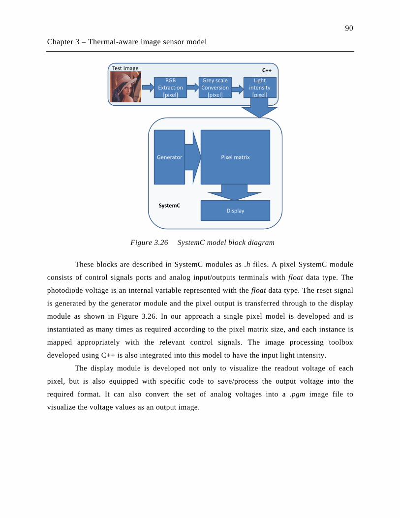
90
Chapter 3 – Thermal-aware image sensor model
These blocks are described in SystemC modules as .h files. A pixel SystemC module
consists of control signals ports and analog input/outputs terminals with float data type. The
photodiode voltage is an internal variable represented with the float data type. The reset signal
is generated by the generator module and the pixel output is transferred through to the display
module as shown in Figure 3.26. In our approach a single pixel model is developed and is
instantiated as many times as required according to the pixel matrix size, and each instance is
mapped appropriately with the relevant control signals. The image processing toolbox
developed using C++ is also integrated into this model to have the input light intensity.
The display module is developed not only to visualize the readout voltage of each
pixel, but is also equipped with specific code to save/process the output voltage into the
required format. It can also convert the set of analog voltages into a .pgm image file to
visualize the voltage values as an output image.
Generator Pixel matrix
DisplaySystemC
RGB Extraction
[pixel]
Grey scaleConversion
[pixel]
Light intensity
[pixel]
Test Image C++
Figure 3.26 SystemC model block diagram
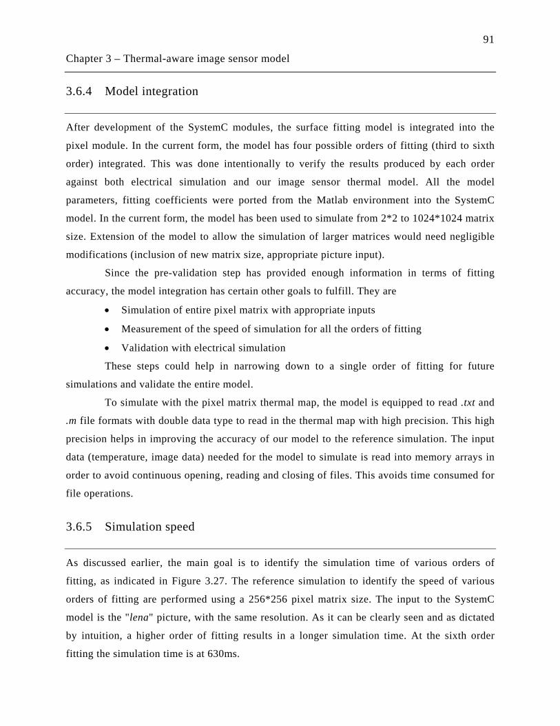
91
Chapter 3 – Thermal-aware image sensor model
3.6.4 Model integration
After development of the SystemC modules, the surface fitting model is integrated into the
pixel module. In the current form, the model has four possible orders of fitting (third to sixth
order) integrated. This was done intentionally to verify the results produced by each order
against both electrical simulation and our image sensor thermal model. All the model
parameters, fitting coefficients were ported from the Matlab environment into the SystemC
model. In the current form, the model has been used to simulate from 2*2 to 1024*1024 matrix
size. Extension of the model to allow the simulation of larger matrices would need negligible
modifications (inclusion of new matrix size, appropriate picture input).
Since the pre-validation step has provided enough information in terms of fitting
accuracy, the model integration has certain other goals to fulfill. They are
• Simulation of entire pixel matrix with appropriate inputs
• Measurement of the speed of simulation for all the orders of fitting
• Validation with electrical simulation
These steps could help in narrowing down to a single order of fitting for future
simulations and validate the entire model.
To simulate with the pixel matrix thermal map, the model is equipped to read .txt and
.m file formats with double data type to read in the thermal map with high precision. This high
precision helps in improving the accuracy of our model to the reference simulation. The input
data (temperature, image data) needed for the model to simulate is read into memory arrays in
order to avoid continuous opening, reading and closing of files. This avoids time consumed for
file operations.
3.6.5 Simulation speed
As discussed earlier, the main goal is to identify the simulation time of various orders of
fitting, as indicated in Figure 3.27. The reference simulation to identify the speed of various
orders of fitting are performed using a 256*256 pixel matrix size. The input to the SystemC
model is the "lena" picture, with the same resolution. As it can be clearly seen and as dictated
by intuition, a higher order of fitting results in a longer simulation time. At the sixth order
fitting the simulation time is at 630ms.
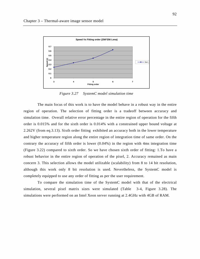
92
Chapter 3 – Thermal-aware image sensor model
The main focus of this work is to have the model behave in a robust way in the entire
region of operation. The selection of fitting order is a tradeoff between accuracy and
simulation time. Overall relative error percentage in the entire region of operation for the fifth
order is 0.015% and for the sixth order is 0.014% with a constrained upper bound voltage at
2.262V (from eq.3.13). Sixth order fitting exhibited an accuracy both in the lower temperature
and higher temperature region along the entire region of integration time of same order. On the
contrary the accuracy of fifth order is lower (0.04%) in the region with 4ms integration time
(Figure 3.22) compared to sixth order. So we have chosen sixth order of fitting: 1.To have a
robust behavior in the entire region of operation of the pixel, 2. Accuracy remained as main
concern 3. This selection allows the model utilizable (scalability) from 8 to 14 bit resolution,
although this work only 8 bit resolution is used. Nevertheless, the SystemC model is
completely equipped to use any order of fitting as per the user requirement.
To compare the simulation time of the SystemC model with that of the electrical
simulation, several pixel matrix sizes were simulated (Table 3-4, Figure 3.28). The
simulations were performed on an Intel Xeon server running at 2.4GHz with 4GB of RAM.
Figure 3.27 SystemC model simulation time
0
0.1
0.2
0.3
0.4
0.5
0.6
0.7
3 4 5 6 7
Spee
d (s
)
Fitting order
Speed Vs Fitting order (256*256 Lena)
Seri…
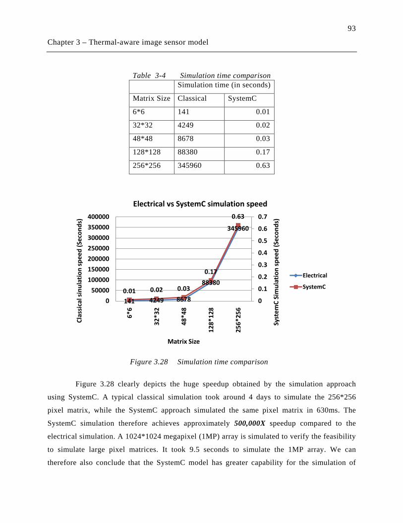
93
Chapter 3 – Thermal-aware image sensor model
Table 3-4 Simulation time comparison
Simulation time (in seconds)
Matrix Size Classical SystemC
6*6 141 0.01
32*32 4249 0.02
48*48 8678 0.03
128*128 88380 0.17
256*256 345960 0.63
Figure 3.28 clearly depicts the huge speedup obtained by the simulation approach
using SystemC. A typical classical simulation took around 4 days to simulate the 256*256
pixel matrix, while the SystemC approach simulated the same pixel matrix in 630ms. The
SystemC simulation therefore achieves approximately 500,000X speedup compared to the
electrical simulation. A 1024*1024 megapixel (1MP) array is simulated to verify the feasibility
to simulate large pixel matrices. It took 9.5 seconds to simulate the 1MP array. We can
therefore also conclude that the SystemC model has greater capability for the simulation of
141 4249 8678
88380
345960
0.01 0.02 0.03
0.17
0.63
0
0.1
0.2
0.3
0.4
0.5
0.6
0.7
050000
100000150000200000250000300000350000400000
6*6
32*3
2
48*4
8
128*
128
256*
256
Syst
emC
Sim
ulat
ion
spee
d (S
econ
ds)
Clas
sica
l sin
ulat
ion
spee
d (S
econ
ds)
Matrix Size
Electrical vs SystemC simulation speed
Electrical
SystemC
Figure 3.28 Simulation time comparison
94
Chapter 3 – Thermal-aware image sensor model
large pixel matrices. This size cannot be simulated using Cadence Spectre (or any Spice-based
simulator).
SystemC simulation time for the 6*6 or 32*32 is much faster but they are having an
influence from the image, thermal map read/write/open/close operations involved which takes
significant amount of time. This simulation model not only alleviates the problem of
simulating large pixel matrices, but also helps the designer to analyze the impact of pixel
behavior at early stages of system design, due to the high speed simulation and the tunable
accuracy available from the model.
3.7 Post-validation
3.7.1 Matrix simulation
The pre-validation step provided the necessary behavior of the pixel for grey scale intensity
(image) and the temperature impact (thermal map). The integration step provided the
simulation behavior and its speed for different pixel matrix sizes. The next step is to simulate
an entire pixel matrix with a test image input and several thermal maps. This will enable the
evaluation of the robustness of the model integrated into the SystemC environment. To start
the preliminary post validation, a homogenous distribution of temperature is taken across the
pixel matrix. This is performed to validate the model and to see if all the pixels behave the
same way with homogenous temperature distribution.
To perform this validation, several electrical simulations were performed for the same
input image at different homogeneous temperatures, as depicted in Figure 3.29.
For the Cadence Spectre reference simulation, a Skill™ function based interface [16]
was developed to decode the image into light intensity values to be fed into the pixel matrix.
This toolbox was developed to help designers handle millions of pixels easily. The toolbox
uses the same resolution as the image sensor. Sampling times can be fixed to fetch the readout
voltage of each pixel. This toolbox helps in feeding the image input and obtains the readout
voltage of each pixel. Generally, designers tend to simulate only small groups of pixels to
validate the global simulation, using approaches based on TCAD at the physical level [16].
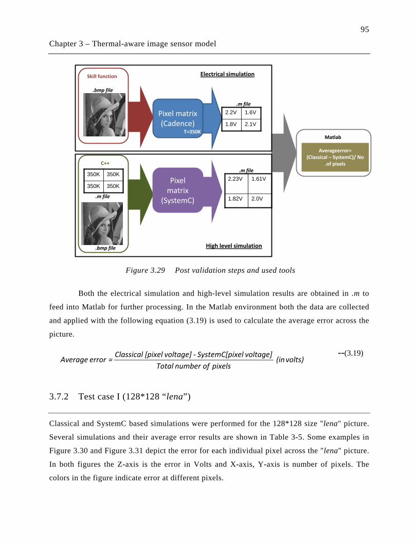
95
Chapter 3 – Thermal-aware image sensor model
Both the electrical simulation and high-level simulation results are obtained in .m to
feed into Matlab for further processing. In the Matlab environment both the data are collected
and applied with the following equation (3.19) is used to calculate the average error across the
picture.
--(3.19)
3.7.2 Test case I (128*128 “lena”)
Classical and SystemC based simulations were performed for the 128*128 size "lena" picture.
Several simulations and their average error results are shown in Table 3-5. Some examples in
Figure 3.30 and Figure 3.31 depict the error for each individual pixel across the "lena" picture.
In both figures the Z-axis is the error in Volts and X-axis, Y-axis is number of pixels. The
colors in the figure indicate error at different pixels.
Pixel matrix(Cadence)
350K 350K
350K 350K
2.2V 1.6V
1.8V 2.1VT=350K
.m file
.m file
.bmp file
.bmp file
2.23V 1.61V
1.82V 2.0V
.m file
Skill function
C++
Averageerror= (Classical – SystemC)/ No
.of pixels
Matlab
Pixel matrix
(SystemC)
Electrical simulation
High level simulation
Figure 3.29 Post validation steps and used tools
volts) (in pixelsof numberTotal
voltage]xel SystemC[pi-voltage][pixel Classical =error Average
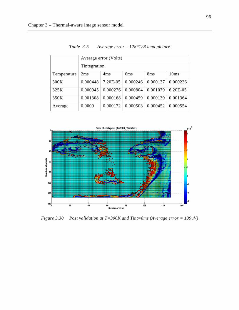
96
Chapter 3 – Thermal-aware image sensor model
Table 3-5 Average error – 128*128 lena picture
Average error (Volts)
Tintegration
Temperature 2ms 4ms 6ms 8ms 10ms
300K 0.000448 7.20E-05 0.000246 0.000137 0.000236
325K 0.000945 0.000276 0.000804 0.001079 6.20E-05
350K 0.001308 0.000168 0.000459 0.000139 0.001364
Average 0.0009 0.000172 0.000503 0.000452 0.000554
Figure 3.30 Post validation at T=300K and Tint=8ms (Average error = 139uV)
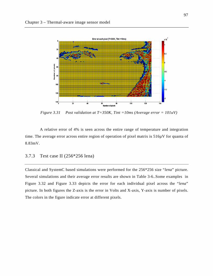
97
Chapter 3 – Thermal-aware image sensor model
A relative error of 4% is seen across the entire range of temperature and integration
time. The average error across entire region of operation of pixel matrix is 516µV for quanta of
8.83mV.
3.7.3 Test case II (256*256 lena)
Classical and SystemC based simulations were performed for the 256*256 size “lena” picture.
Several simulations and their average error results are shown in Table 3-6..Some examples in
Figure 3.32 and Figure 3.33 depicts the error for each individual pixel across the “lena”
picture. In both figures the Z-axis is the error in Volts and X-axis, Y-axis is number of pixels.
The colors in the figure indicate error at different pixels.
Figure 3.31 Post validation at T=350K, Tint =10ms (Average error = 101uV)
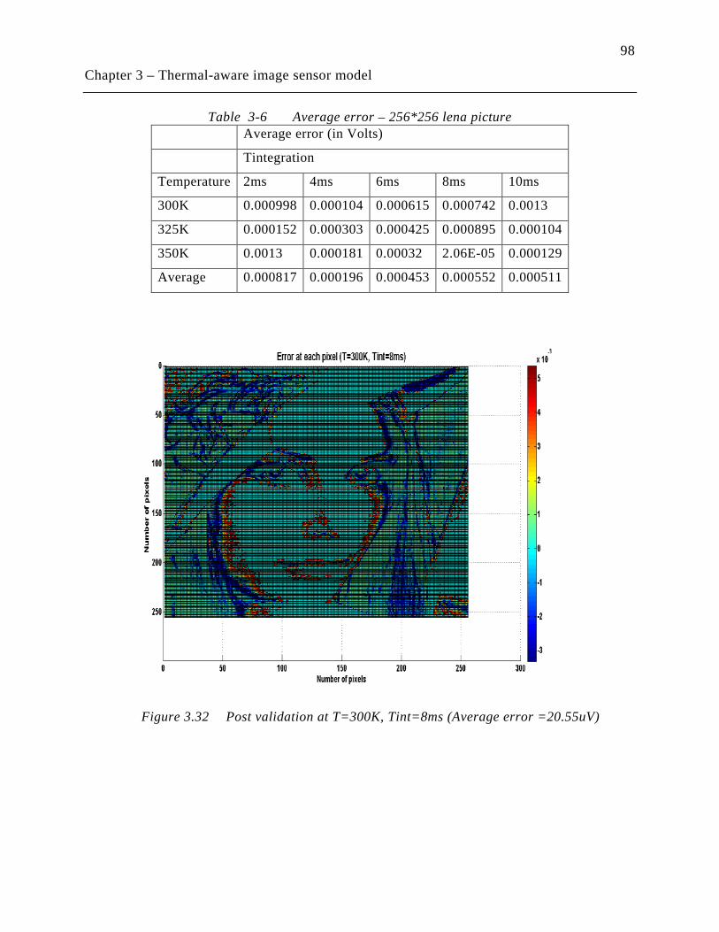
98
Chapter 3 – Thermal-aware image sensor model
Table 3-6 Average error – 256*256 lena picture Average error (in Volts)
Tintegration
Temperature 2ms 4ms 6ms 8ms 10ms
300K 0.000998 0.000104 0.000615 0.000742 0.0013
325K 0.000152 0.000303 0.000425 0.000895 0.000104
350K 0.0013 0.000181 0.00032 2.06E-05 0.000129
Average 0.000817 0.000196 0.000453 0.000552 0.000511
Figure 3.32 Post validation at T=300K, Tint=8ms (Average error =20.55uV)
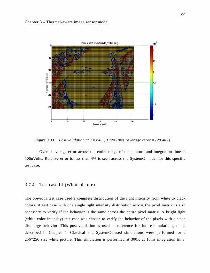
99
Chapter 3 – Thermal-aware image sensor model
Overall average error across the entire range of temperature and integration time is
506uVolts. Relative error is less than 4% is seen across the SystemC model for this specific
test case.
3.7.4 Test case III (White picture)
The previous test case used a complete distribution of the light intensity from white to black
colors. A test case with one single light intensity distribution across the pixel matrix is also
necessary to verify if the behavior is the same across the entire pixel matrix. A bright light
(white color intensity) test case was chosen to verify the behavior of the pixels with a steep
discharge behavior. This post-validation is used as reference for future simulations, to be
described in Chapter 4. Classical and SystemC-based simulations were performed for a
256*256 size white picture. This simulation is performed at 300K at 10ms integration time.
Figure 3.33 Post validation at T=350K, Tint=10ms (Average error =129.4uV)
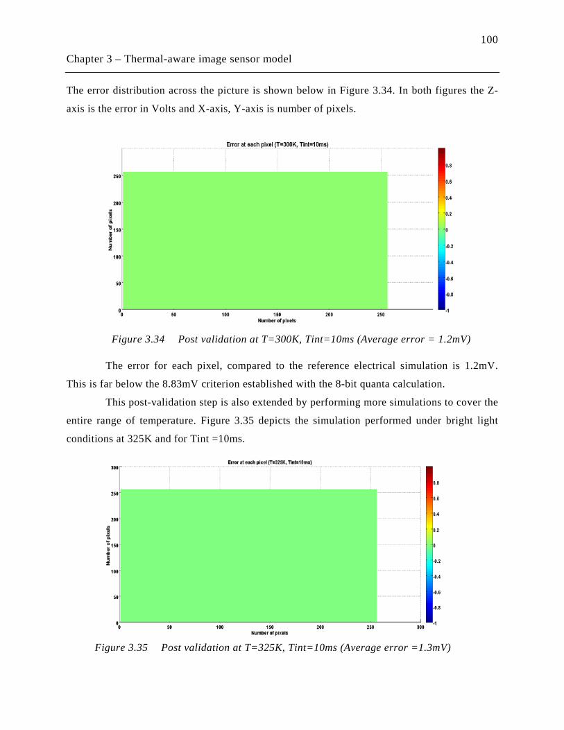
100
Chapter 3 – Thermal-aware image sensor model
The error distribution across the picture is shown below in Figure 3.34. In both figures the Z-
axis is the error in Volts and X-axis, Y-axis is number of pixels.
The error for each pixel, compared to the reference electrical simulation is 1.2mV.
This is far below the 8.83mV criterion established with the 8-bit quanta calculation.
This post-validation step is also extended by performing more simulations to cover the
entire range of temperature. Figure 3.35 depicts the simulation performed under bright light
conditions at 325K and for Tint =10ms.
Figure 3.34 Post validation at T=300K, Tint=10ms (Average error = 1.2mV)
Figure 3.35 Post validation at T=325K, Tint=10ms (Average error =1.3mV)
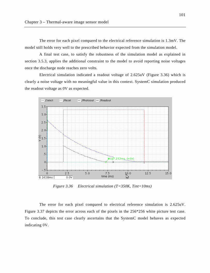
101
Chapter 3 – Thermal-aware image sensor model
The error for each pixel compared to the electrical reference simulation is 1.3mV. The
model still holds very well to the prescribed behavior expected from the simulation model.
A final test case, to satisfy the robustness of the simulation model as explained in
section 3.5.3, applies the additional constraint to the model to avoid reporting noise voltages
once the discharge node reaches zero volts.
Electrical simulation indicated a readout voltage of 2.625uV (Figure 3.36) which is
clearly a noise voltage with no meaningful value in this context. SystemC simulation produced
the readout voltage as 0V as expected.
The error for each pixel compared to electrical reference simulation is 2.625uV.
Figure 3.37 depicts the error across each of the pixels in the 256*256 white picture test case.
To conclude, this test case clearly ascertains that the SystemC model behaves as expected
indicating 0V.
Figure 3.36 Electrical simulation (T=350K, Tint=10ms)
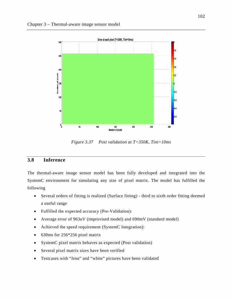
102
Chapter 3 – Thermal-aware image sensor model
3.8 Inference
The thermal-aware image sensor model has been fully developed and integrated into the
SystemC environment for simulating any size of pixel matrix. The model has fulfilled the
following
• Several orders of fitting is realized (Surface fitting) - third to sixth order fitting deemed
a useful range
• Fulfilled the expected accuracy (Pre-Validation):
• Average error of 963uV (improvised model) and 690mV (standard model)
• Achieved the speed requirement (SystemC Integration):
• 630ms for 256*256 pixel matrix
• SystemC pixel matrix behaves as expected (Post validation)
• Several pixel matrix sizes have been verified
• Testcases with “lena” and “white” pictures have been validated
Figure 3.37 Post validation at T=350K, Tint=10ms
103
Chapter 3 – Thermal-aware image sensor model
The above results and validation have provided a model which is flexible to be
integrated with other tools such as Hotspot [5] (thermal simulator) or a floorplanner to perform
various experiments. This will be dealt in the next chapter.
Bibliography
[1] H.Tian, “Noise analysis in CMOS Image sensor” August 2000, Thesis, Stanford university
[2] S. Decker, D. McGrath, K. Brehmer, and C. G. Sodini “A 256x256 MOS Imaging Array with Wide Dynamic Range Pixels and ColumnParallel Digital Output. IEEE J. Solid-State Circuits, 33(12):20812091, 1998.
[3] O. Yadid-Pecht, B. Mansoorian, E. R. Fossum, and B. Pain. “Optimization of Noise and Responsivity in CMOS Active Pixel Sensors for Detection of Ultra Low Light Levels”, In Proc. SPIE, volume 3019, pages 125136, San Jose, CA, Feb. 1997
[4] S. K. Mendis, S. E. Kemeny, R. C. Gee, B. Pain, C. O. Staller, Q. Kim, and E. R. Fossum. “CMOS Active Pixel Image Sensors for Highly Integrated Imaging Systems”, IEEE J. Solid-State Circuits, 32(2):187197, 1997.
[5] K. Skadron, K. Sankaranarayanan, S. Velusamy, D. Tarjan, M.R. Stan, and W. Huang. “Temperature-Aware Microarchitecture: Modeling and Implementation.” ACM Transactions on Architecture and Code Optimization, 1(1):94-125, Mar. 2004
[6] S.Mendis, S.E.Kemeny, E.Fossum, “CMOS Active pixel image sensor » IEEE transactions on electron devices, vol 41, No.3, March 1994
[7] M.Bigas, E.Cabruja, J.Forest and J.Salvi, “Review of CMOS image Sensors” Microelectronic Journal,2006,37,433-451
[8] S.Kavusi, A.El Gamal, “Quantitative study of high dynamic range image sensor architecture”, Proc. of SPIE-IS&T Electronic Imaging, SPIE Vol. 5301 ,2004
104
Chapter 3 – Thermal-aware image sensor model
[9] J.Krammer, Luc Hebrard, “Pixel schematic accessed through 3D IDEAS collaboration”
[10] M.G. Cox and J.G.Hayes, “Curve fitting: A guide and suite of algorithms for the non-specialist user NPL report NAC 26 National physical laboratory, 1973
[11] Wolfram Mathworld: “Polynomial”
[12] http://www.mathworks.com/moler/interp.pdf
[13] Open SystemC Initiative: http://www.systemc.org
[14] Yarom.I., Glasser G., ,Proceedings of ICECS 2004, 13-15 Dec. 2004 p.:507 - 510.
[15] Habibi A., Moinudeen H et al., “ Towards faster simulation of SystemC designs “, Emerging VLSI Technologies and Architectures, IEEE, 2-3 March 2006, Vol.00 p:2 pp
[16] Navarro.D, Feng.Z,Viswanathan.V et al., “Imager toolbox for CMOS image sensors in Cadence ADE “, Demset 2011, Orlando, Florida, USA, Nov 29th – Dec2nd, 2011
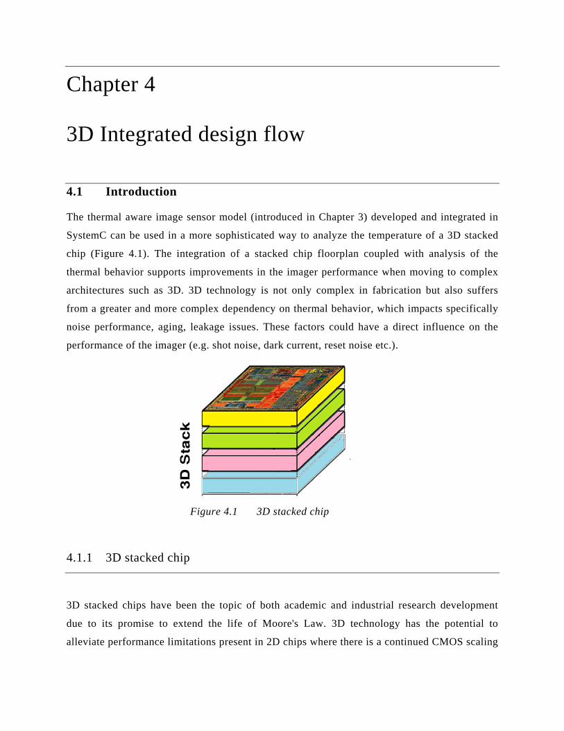
Chapter 4
4.1 Introduction
3D Integrated design flow
The thermal aware image sensor model (introduced in Chapter 3) developed and integrated in
SystemC can be used in a more sophisticated way to analyze the temperature of a 3D stacked
chip (Figure 4.1). The integration of a stacked chip floorplan coupled with analysis of the
thermal behavior supports improvements in the imager performance when moving to complex
architectures such as 3D. 3D technology is not only complex in fabrication but also suffers
from a greater and more complex dependency on thermal behavior, which impacts specifically
noise performance, aging, leakage issues. These factors could have a direct influence on the
performance of the imager (e.g. shot noise, dark current, reset noise etc.).
4.1.1 3D stacked chip
3D stacked chips have been the topic of both academic and industrial research development
due to its promise to extend the life of Moore's Law. 3D technology has the potential to
alleviate performance limitations present in 2D chips where there is a continued CMOS scaling
Figure 4.1 3D stacked chip

106
Chapter 4 – 3D integrated design flow
trend [1][2][3], and in particular to overcome the interconnect bottleneck which exist in 2D
chips. By using the vertical dimension, chip size is automatically reduced by a factor
equivalent to the number of stacked levels, such that the maximum length of wires is reduced,
leading to a lower number of repeaters or buffer and consequently better circuit speed
performance. The 3D integration approach further has the potential to combine different
technology layers [4] such as digital, analog, optical in a single chip.
Although there are many advantages in using 3D, it does suffer from issues such as
power density, integration yield and test coverage. In particular, power density increases with
the number of layers integrated on top of each other, the natural consequence being that the
temperature dissipation also increases many-fold [5]. In a conventional 2D chip the heat sink
area evacuates heat over the entire surface of active elements, but 3D integration decreases the
chip footprint (and stacks layers of active elements above each other) and therefore increases
the power density while at the same time reducing the area of the heat sink interface, so the
heat sink cannot evacuate the high temperature. The analysis and reduction of the thermal
impact is therefore mandatory in any consideration of 3D technology.
In this chapter we will discuss in more detail the thermal model integration into the
3D platform. In section 4.2 we will detail the floorplanner, followed by the thermal evaluation
tool in section 4.3. The integration of the thermal-aware imager model in the integrated
environment will be discussed in section 4.4 followed by results of the tool in section with
various test cases in section 4.5. The thermal impact and its effects will be correlated with the
imager performance as and when required. Finally, inferences will be drawn from the test cases
in section 4.6.
4.1.2 Integrated design flow
The thermal aware image sensor model demonstrated in Chapter 3 is accurate, and simulates at
a speed compatible with system-level simulation. In order to simulate the performance of the
imager level in the 3D stack, we require a tool which will extract a thermal map from the 3D
stack thermal model, and inject this thermal map into the thermal-aware image sensor model.
In addition to the thermal map and as we have seen in the previous chapter, the imager thermal
model needs light intensity and integration time inputs as shown in Figure 4.2.
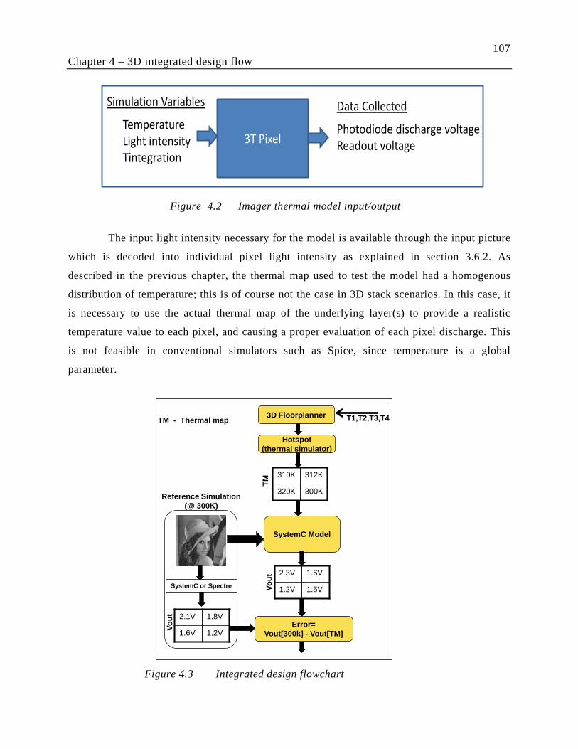
107
Chapter 4 – 3D integrated design flow
The input light intensity necessary for the model is available through the input picture
which is decoded into individual pixel light intensity as explained in section 3.6.2. As
described in the previous chapter, the thermal map used to test the model had a homogenous
distribution of temperature; this is of course not the case in 3D stack scenarios. In this case, it
is necessary to use the actual thermal map of the underlying layer(s) to provide a realistic
temperature value to each pixel, and causing a proper evaluation of each pixel discharge. This
is not feasible in conventional simulators such as Spice, since temperature is a global
parameter.
3T PixelTemperatureLight intensityTintegration
Simulation Variables Data Collected
Photodiode discharge voltageReadout voltage
Figure 4.3 Integrated design flowchart
Figure 4.2 Imager thermal model input/output
3D Floorplanner
Hotspot(thermal simulator)
SystemC Model
310K 312K
320K 300KReference Simulation(@ 300K)
2.3V 1.6V
1.2V 1.5V
2.1V 1.8V
1.6V 1.2VError=
Vout[300k] - Vout[TM]
T1,T2,T3,T4
Vout
Vout
TM
TM - Thermal map
SystemC or Spectre
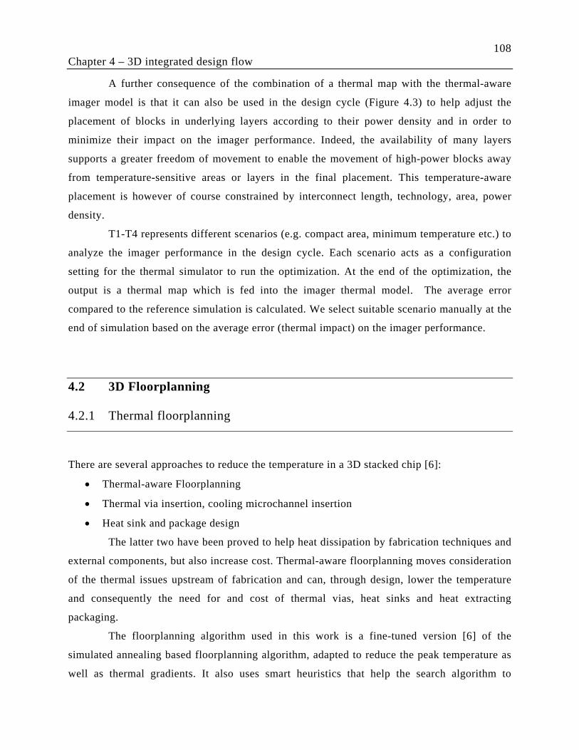
108
Chapter 4 – 3D integrated design flow
A further consequence of the combination of a thermal map with the thermal-aware
imager model is that it can also be used in the design cycle (Figure 4.3) to help adjust the
placement of blocks in underlying layers according to their power density and in order to
minimize their impact on the imager performance. Indeed, the availability of many layers
supports a greater freedom of movement to enable the movement of high-power blocks away
from temperature-sensitive areas or layers in the final placement. This temperature-aware
placement is however of course constrained by interconnect length, technology, area, power
density.
T1-T4 represents different scenarios (e.g. compact area, minimum temperature etc.) to
analyze the imager performance in the design cycle. Each scenario acts as a configuration
setting for the thermal simulator to run the optimization. At the end of the optimization, the
output is a thermal map which is fed into the imager thermal model. The average error
compared to the reference simulation is calculated. We select suitable scenario manually at the
end of simulation based on the average error (thermal impact) on the imager performance.
4.2 3D Floorplanning
4.2.1 Thermal floorplanning
There are several approaches to reduce the temperature in a 3D stacked chip [6]:
• Thermal-aware Floorplanning
• Thermal via insertion, cooling microchannel insertion
• Heat sink and package design
The latter two have been proved to help heat dissipation by fabrication techniques and
external components, but also increase cost. Thermal-aware floorplanning moves consideration
of the thermal issues upstream of fabrication and can, through design, lower the temperature
and consequently the need for and cost of thermal vias, heat sinks and heat extracting
packaging.
The floorplanning algorithm used in this work is a fine-tuned version [6] of the
simulated annealing based floorplanning algorithm, adapted to reduce the peak temperature as
well as thermal gradients. It also uses smart heuristics that help the search algorithm to
109
Chapter 4 – 3D integrated design flow
converge to thermally efficient solutions. Since our objective is to achieve a better imager
performance through reduction of the influence of temperature, we explore the use of this
floorplanning algorithm in conjunction with the 3D integrated design flow. In the following
paragraphs we give a brief description of the algorithm and its use.
4.2.2 Floorplanner algorithm
Primarily this work is a parallel research work going on in our group which focuses on
architectural exploration using Parquet 2D floorplanner and HotSpot tool. Part of this work and
its improvements are utilized to realize the 3D integrated design flow.
The floorplanner tool is adapted from the Parquet 2D floorplanner [7], where the
floorplanning algorithm is based on simulated annealing. The problem is formulated for the 3D
case [6] as follows: B=b1, b2, …, bm are the set of rectangular blocks with height hi and
width wi having terminals T=t1, t2,…, tp. Pi are the pins that connect the various blocks
and terminals, while L=li|1≤ i ≤ n are the set of n layers.
Let (xj,yj ,l j) denote the coordinates of terminal t j and (xi,yi ,l i) denote the coordinates
of block bi . The 3D floorplanning problem is to find a solution S for the assignment of blocks
coordinates (xi,yi ,l i
For a 3D stacked IC problem, the circuit and the stack descriptions are necessary. The
circuit description indicates the size, power and connectivity of the blocks, while the stack
description indicates over how many and of what types of layers the blocks can be arranged. It
is important to be able to realise various kinds of optimization (area, wirelength, temperature)
for the technology nodes used in each layer. Apart from area minimization, the connectivity
between blocks as well as the I/O pad positions are required in order to be able to optimize the
wirelength. Material conductivities, and stack geometries are necessary for temperature
minimization. The workflow is illustrated in
) so that no two blocks overlap and a cost function C(S) is minimized. In
the implemented optimization, the solution is initialized to a random floorplan. The solution is
incrementally improved until the optimization times out. The solution quality depends on the
starting point and how much time the algorithm is allowed to spent refining it. Increasing the
optimization time reduces the dependency of the solution quality on the starting point.
Figure 4.4.
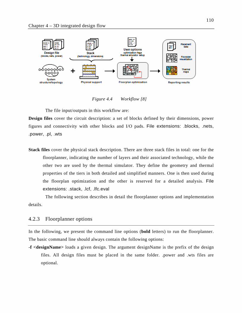
110
Chapter 4 – 3D integrated design flow
The file input/outputs in this workflow are:
Design files cover the circuit description: a set of blocks defined by their dimensions, power
figures and connectivity with other blocks and I/O pads. File extensions: .blocks, .nets,
.power, .pl, .wts
Stack files cover the physical stack description. There are three stack files in total: one for the
floorplanner, indicating the number of layers and their associated technology, while the
other two are used by the thermal simulator. They define the geometry and thermal
properties of the tiers in both detailed and simplified manners. One is then used during
the floorplan optimization and the other is reserved for a detailed analysis. File
extensions: .stack, .lcf, .lfc.eval
The following section describes in detail the floorplanner options and implementation
details.
4.2.3 Floorplanner options
In the following, we present the command line options (bold letters) to run the floorplanner.
The basic command line should always contain the following options:
-f <designName> loads a given design. The argument designName is the prefix of the design
files. All design files must be placed in the same folder. .power and .wts files are
optional.
Figure 4.4 Workflow [8]

111
Chapter 4 – 3D integrated design flow
-stack <stackName> specifies the use of a given stack. The only stack file mandatory is the
.stack. The other two files are necessary if thermal simulation is activated. Again, all
files describing a stack must be in the same folder.
Apart from the basic command line arguments there are other user options which give
means to control the optimization process. The user can control the random seend generator
and runtime (number of iterations), change the optimization objectives or modify the thermal
simulator setup. With these options the user has the possibility to achieve better solutions
and/or repeat experiments.
-n <p>produce p independent runs (different seeds). The console output reports the minimum,
average and maximum values attained for the various quality measures (wirelength,
temperature, etc). Default 1.
-s <q> set the random generator to use the seed q (integer). To reproduce a given result, we
initialize the random generator with same starting point and store all the seeds
generated. The stored file is used in the optimization to guarantee the result
reproduction. Default random.
-seedlist <seedsFile> is a combination of the first two options. The tool runs for each seed
value declared in seedsFile. This mechanism allows the impact of different options to
be compared in a statistical manner. Default not used.
-maxIter <k> sets the maximum number of iterations (solutions visited) before the algorithm
stops. To scale with the size of the problem, the actual maximum number of iterations
is obtained multiplying k by the number of blocks (maxIter = k * nblocks
-noScaleTerms The positions declared in the placement file are used and kept unchanged
(
). Default 2000.
The position [8] of the I/O terminals (pads) is an important factor for floorplanning.
Different assignments will lead to different floorplan solutions, with the placement of the
blocks close to the terminals to which they are connected.
In a first approach, the actual pad position may not be known, as well as the
dimensions of the floorplan outline (core outline). Therefore, three ways to process the
terminal positions are available.
Figure 4.5(a)). The actual floorplan outline can either be contained in or exceed the outline
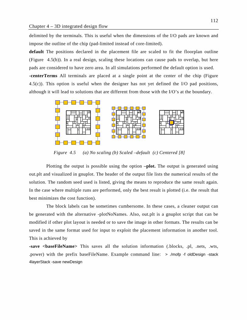
112
Chapter 4 – 3D integrated design flow
delimited by the terminals. This is useful when the dimensions of the I/O pads are known and
impose the outline of the chip (pad-limited instead of core-limited).
default The positions declared in the placement file are scaled to fit the floorplan outline
(Figure 4.5(b)). In a real design, scaling these locations can cause pads to overlap, but here
pads are considered to have zero area. In all simulations performed the default option is used.
-centerTerms All terminals are placed at a single point at the center of the chip (Figure
4.5(c)). This option is useful when the designer has not yet defined the I/O pad positions,
although it will lead to solutions that are different from those with the I/O’s at the boundary.
Plotting the output is possible using the option –plot. The output is generated using
out.plt and visualized in gnuplot. The header of the output file lists the numerical results of the
solution. The random seed used is listed, giving the means to reproduce the same result again.
In the case where multiple runs are performed, only the best result is plotted (i.e. the result that
best minimizes the cost function).
The block labels can be sometimes cumbersome. In these cases, a cleaner output can
be generated with the alternative -plotNoNames. Also, out.plt is a gnuplot script that can be
modified if other plot layout is needed or to save the image in other formats. The results can be
saved in the same format used for input to exploit the placement information in another tool.
This is achieved by
-save <baseFileName> This saves all the solution information (.blocks, .pl, .nets, .wts,
.power) with the prefix baseFileName. Example command line: > ./mofp -f oldDesign -stack
4layerStack -save newDesign
Figure 4.5 (a) No scaling (b) Scaled –default (c) Centered [8]
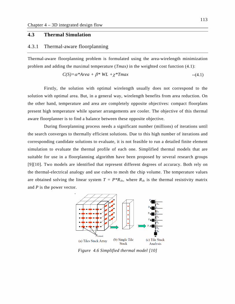
113
Chapter 4 – 3D integrated design flow
4.3 Thermal Simulation
4.3.1 Thermal-aware floorplanning
Thermal-aware floorplanning problem is formulated using the area-wirelength minimization
problem and adding the maximal temperature (Tmax) in the weighted cost function (4.1):
C(S)=α*Area + β* WL +χ*Tmax
--(4.1)
Firstly, the solution with optimal wirelength usually does not correspond to the
solution with optimal area. But, in a general way, wirelength benefits from area reduction. On
the other hand, temperature and area are completely opposite objectives: compact floorplans
present high temperature while sparser arrangements are cooler. The objective of this thermal
aware floorplanner is to find a balance between these opposite objective.
During floorplanning process needs a significant number (millions) of iterations until
the search converges to thermally efficient solutions. Due to this high number of iterations and
corresponding candidate solutions to evaluate, it is not feasible to run a detailed finite element
simulation to evaluate the thermal profile of each one. Simplified thermal models that are
suitable for use in a floorplanning algorithm have been proposed by several research groups
[9][10]. Two models are identified that represent different degrees of accuracy. Both rely on
the thermal-electrical analogy and use cubes to mesh the chip volume. The temperature values
are obtained solving the linear system T = P*Rth , where Rth
is the thermal resistivity matrix
and P is the power vector.
Figure 4.6 Simplified thermal model [10]
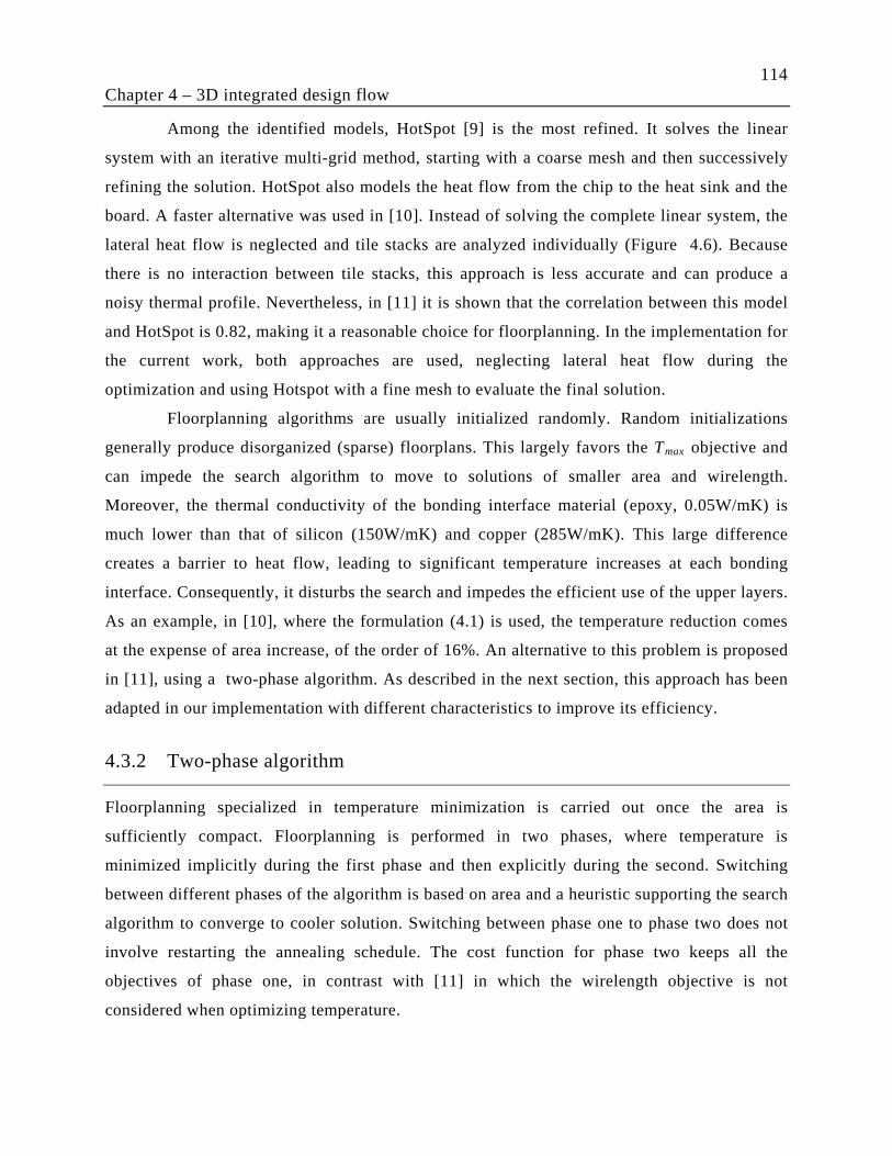
114
Chapter 4 – 3D integrated design flow
Among the identified models, HotSpot [9] is the most refined. It solves the linear
system with an iterative multi-grid method, starting with a coarse mesh and then successively
refining the solution. HotSpot also models the heat flow from the chip to the heat sink and the
board. A faster alternative was used in [10]. Instead of solving the complete linear system, the
lateral heat flow is neglected and tile stacks are analyzed individually (Figure 4.6). Because
there is no interaction between tile stacks, this approach is less accurate and can produce a
noisy thermal profile. Nevertheless, in [11] it is shown that the correlation between this model
and HotSpot is 0.82, making it a reasonable choice for floorplanning. In the implementation for
the current work, both approaches are used, neglecting lateral heat flow during the
optimization and using Hotspot with a fine mesh to evaluate the final solution.
Floorplanning algorithms are usually initialized randomly. Random initializations
generally produce disorganized (sparse) floorplans. This largely favors the Tmax
4.3.2 Two-phase algorithm
objective and
can impede the search algorithm to move to solutions of smaller area and wirelength.
Moreover, the thermal conductivity of the bonding interface material (epoxy, 0.05W/mK) is
much lower than that of silicon (150W/mK) and copper (285W/mK). This large difference
creates a barrier to heat flow, leading to significant temperature increases at each bonding
interface. Consequently, it disturbs the search and impedes the efficient use of the upper layers.
As an example, in [10], where the formulation (4.1) is used, the temperature reduction comes
at the expense of area increase, of the order of 16%. An alternative to this problem is proposed
in [11], using a two-phase algorithm. As described in the next section, this approach has been
adapted in our implementation with different characteristics to improve its efficiency.
Floorplanning specialized in temperature minimization is carried out once the area is
sufficiently compact. Floorplanning is performed in two phases, where temperature is
minimized implicitly during the first phase and then explicitly during the second. Switching
between different phases of the algorithm is based on area and a heuristic supporting the search
algorithm to converge to cooler solution. Switching between phase one to phase two does not
involve restarting the annealing schedule. The cost function for phase two keeps all the
objectives of phase one, in contrast with [11] in which the wirelength objective is not
considered when optimizing temperature.

115
Chapter 4 – 3D integrated design flow
Phase I – Power density distribution
In the first phase a thermally efficient power density distribution is performed as
explained below. From a 1D approximation, the vertical heat flow on the chip as indicated in
Figure 4.7(a) it can be ascertained that a power distribution with a pyramidal shape (Figure
4.7(b)) will implicitly reduce peak temperature.
Therefore, during the first phase, we arrange the blocks in n layers so that the power
density is maximized and the more power-hungry blocks are placed closer to the heat sink. For
this purpose the cost function is written as:
C(S)=α*Area + β* WL +δ∗(1/PDensity --(4.2) )
where PDensity
The q
is a weighted sum of the power density[6] of each layer:
i weighting factor decreases for layers further away from the heat sink. In this
formulation, the term PDensity
Phase 2 – Minimize thermal gradients
is maximized both when the area is reduced and when the power-
hungry blocks are moved to the lower layers. This formulation provides a means to combine
the opposing objectives of area and temperature reduction in the same direction.
Once the area value threshold is achieved and all layers are appropriately occupied,
the second phase commences involving thermal simulations. This threshold must be at least
∑=
⋅=n
ii
iDensity q
AreaPP
1 , with ∑
=
=i
jji RRq
11 --(4.3)
Figure 4.7(a) Vertical heat flow model (b)Power distribution profile that minimizes temperature
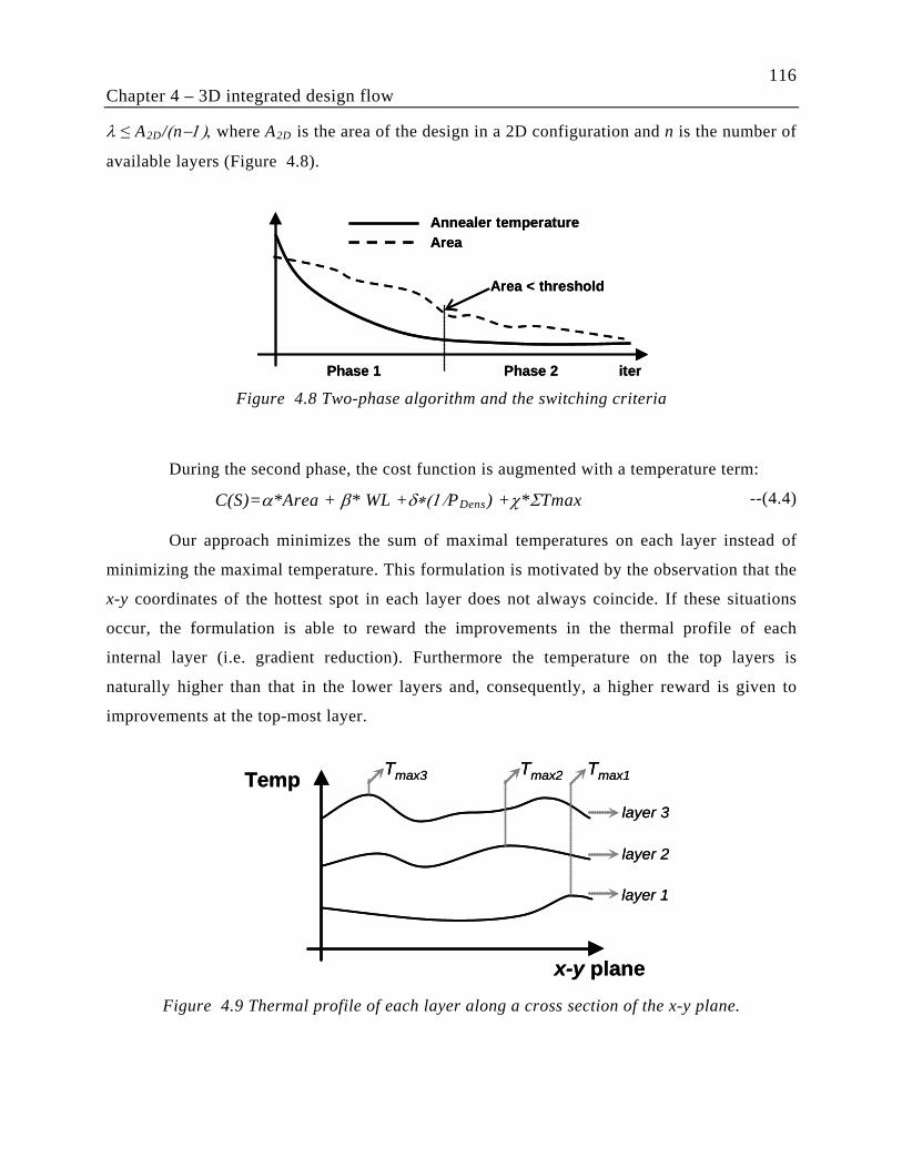
116
Chapter 4 – 3D integrated design flow
λ ≤ A2D/(n−1), where A2D
Figure 4.8
is the area of the design in a 2D configuration and n is the number of
available layers ( ).
iter
Annealer temperature
Phase 1 Phase 2
Area < threshold
Area
iter
Annealer temperature
Phase 1 Phase 2
Area < threshold
Area
Figure 4.8 Two-phase algorithm and the switching criteria
During the second phase, the cost function is augmented with a temperature term:
C(S)=α*Area + β* WL +δ∗(1/PDens) --(4.4) +χ*ΣTmax
Our approach minimizes the sum of maximal temperatures on each layer instead of
minimizing the maximal temperature. This formulation is motivated by the observation that the
x-y coordinates of the hottest spot in each layer does not always coincide. If these situations
occur, the formulation is able to reward the improvements in the thermal profile of each
internal layer (i.e. gradient reduction). Furthermore the temperature on the top layers is
naturally higher than that in the lower layers and, consequently, a higher reward is given to
improvements at the top-most layer.
x-y plane
Temp
layer 1
layer 2
layer 3
Tmax3 Tmax2 Tmax1
x-y plane
Temp
layer 1
layer 2
layer 3
Tmax3 Tmax2 Tmax1
Figure 4.9 Thermal profile of each layer along a cross section of the x-y plane.

117
Chapter 4 – 3D integrated design flow
The power density heuristic consists of biasing all the inter-layer moves in the
direction of attaining a pyramidal power distribution. Therefore, a block bi in layer lk is only
allowed to move to a lower (resp. upper) layer lp if it meets the condition of having a power
density greater (resp. lesser) than the average power density of the blocks in lk . When
performing a 3D move, we randomly select a block in lk
4.3.3 Thermal simulation options
until this condition is satisfied.
The next section describes in detail the various options used in the thermal-aware
floorplanner and its implementation.
When power information is available through the .power file, the user can activate the thermal
simulation with three options:
-evalT Performs a detailed thermal simulation at the end of the optimization. No temperature
minimization is performed. Default off.
-minT Minimizes the temperature using the two phase algorithm. Default off.
-useHeur Activates the use of the power density heuristic. This option enables –evalT and can
either be used alone for a fast thermal-aware floorplanning, or be combined with -minT
to further improve the solution quality. Default off.
The grid size used to discretize the volume can be adjusted to obtain better accuracy.
It can be adjusted to a finer granularity for detailed evaluation and to a coarser granularity
during the iterative optimization process:
-gridEval <size> The grid size used for the detailed evaluation. The value must be a power of
2. Default 32 (32x32 grid).
-gridOpt <size> The grid size used for the simplified vertical model. The value must be a
power of 2. Default 8 (8x8 grid).
-hsConfigFile <filename> is used to replace the default simulator configuration file by a
user defined file.
Using a very fine grid does not imply better results because the simplified thermal
model neglects the lateral heat flow and only takes into account the vertical alignment of heat
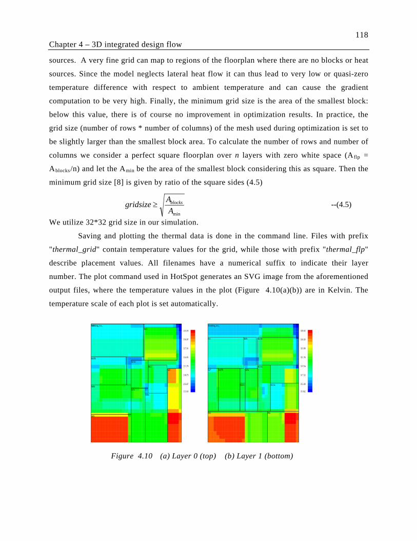
118
Chapter 4 – 3D integrated design flow
sources. A very fine grid can map to regions of the floorplan where there are no blocks or heat
sources. Since the model neglects lateral heat flow it can thus lead to very low or quasi-zero
temperature difference with respect to ambient temperature and can cause the gradient
computation to be very high. Finally, the minimum grid size is the area of the smallest block:
below this value, there is of course no improvement in optimization results. In practice, the
grid size (number of rows * number of columns) of the mesh used during optimization is set to
be slightly larger than the smallest block area. To calculate the number of rows and number of
columns we consider a perfect square floorplan over n layers with zero white space (Aflp =
Ablocks/n) and let the Amin
be the area of the smallest block considering this as square. Then the
minimum grid size [8] is given by ratio of the square sides (4.5)
--(4.5)
We utilize 32*32 grid size in our simulation.
Saving and plotting the thermal data is done in the command line. Files with prefix
"thermal_grid" contain temperature values for the grid, while those with prefix "thermal_flp"
describe placement values. All filenames have a numerical suffix to indicate their layer
number. The plot command used in HotSpot generates an SVG image from the aforementioned
output files, where the temperature values in the plot (Figure 4.10(a)(b)) are in Kelvin. The
temperature scale of each plot is set automatically.
Figure 4.10 (a) Layer 0 (top) (b) Layer 1 (bottom)
minAAgridsize blocks≥
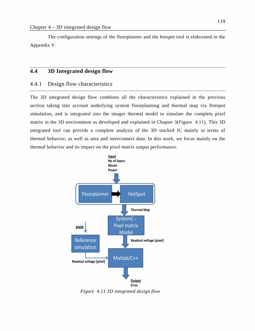
119
Chapter 4 – 3D integrated design flow
The configuration settings of the floorplanner and the hotspot tool is elaborated in the
Appendix V.
4.4 3D Integrated design flow
4.4.1 Design flow characteristics
The 3D integrated design flow combines all the characteristics explained in the previous
section taking into account underlying system floorplanning and thermal map via Hotspot
simulation, and is integrated into the imager thermal model to simulate the complete pixel
matrix in the 3D environment as developed and explained in Chapter 3(Figure 4.11). This 3D
integrated tool can provide a complete analysis of the 3D stacked IC mainly in terms of
thermal behavior, as well as area and interconnect data. In this work, we focus mainly on the
thermal behavior and its impact on the pixel matrix output performance.
Floorplanner HotSpot
Thermal Map
SystemC -Pixel matrix
ModelReadout voltage [pixel]
InputNo of layersBlocksPower
Matlab/C++
OutputError
Reference simulation
Readout voltage [pixel]
300K
Figure 4.11 3D integrated design flow

120
Chapter 4 – 3D integrated design flow
Figure 4.11 depicts the flow of information throughout the complete evaluation
process. Initially, the number of layers, the blocks available in the entire system and their
power values are set. As explained in the previous section, the floorplanning algorithm is run
to obtain a suitable set of layer floorplans with block positions, along with the approximate
thermal profile of each layer. Then the HotSpot tool is run to obtain a more accurate thermal
profile of each layer of the 3D chip.
Both the floorplanning and HotSpot tools were run using a 32*32 grid size. The
thermal map thus obtained is adapted according to the imager pixel matrix size. This process
helps to determine the operating temperature of each pixel.
Simulation of the 3D integrated design flow is necessary to choose the floorplan
which has the lowest thermal influence on the output performance of the imager pixel matrix.
The thermal map obtained from HotSpot is used to provide realistic thermal data per pixel as
input to the SystemC-based imager pixel matrix thermal model. Only the thermal map from the
layer 0 (top most layer) is taken into account for the thermal simulation of the pixel matrix.
The model calculates the readout voltage of each pixel based on the input from the thermal
map and set of input image intensity values.
To verify and select the floorplan which has the lowest influence on the output
performance, a validation step is performed. The validation step involves calculating the error
taking the average of absolute differences of each pixel readout voltage Vout
where T
from the reference
simulation. This is given by
M
𝐴𝐴𝐴𝐴𝐴𝐴𝐴𝐴𝐴𝐴𝐴𝐴𝐴𝐴 𝐴𝐴𝐴𝐴𝐴𝐴𝑒𝑒𝐴𝐴 (𝑉𝑉) =∑ 𝑉𝑉𝑒𝑒𝑜𝑜𝑜𝑜 𝑖𝑖 [300𝐾𝐾] − 𝑉𝑉𝑒𝑒𝑜𝑜𝑜𝑜 𝑖𝑖 [𝑇𝑇𝑀𝑀]𝑖𝑖=𝑁𝑁𝑖𝑖=1
𝑁𝑁
represents the temperature value for the given pixel at the relevant point in the
thermal map of the pixel matrix.
In this case, we have taken the readout voltage error as sole criterion for selection of
the best floorplan. Of course, the overall process can also introduce other metrics for selection,
combining for example temperature impact minimization with area minimization, resulting in a
more complex and longer design cycle. This topic will be covered in detail in the following
sections.
--(4.6)
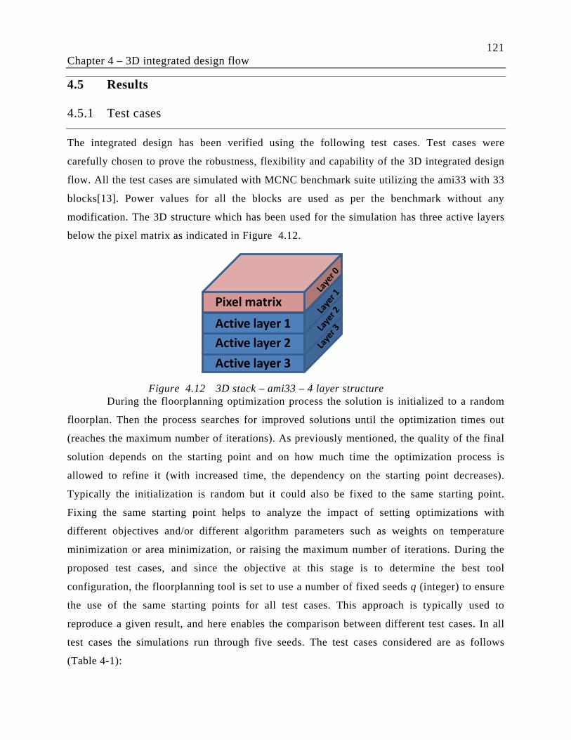
121
Chapter 4 – 3D integrated design flow
4.5 Results
4.5.1 Test cases
The integrated design has been verified using the following test cases. Test cases were
carefully chosen to prove the robustness, flexibility and capability of the 3D integrated design
flow. All the test cases are simulated with MCNC benchmark suite utilizing the ami33 with 33
blocks[13]. Power values for all the blocks are used as per the benchmark without any
modification. The 3D structure which has been used for the simulation has three active layers
below the pixel matrix as indicated in Figure 4.12.
During the floorplanning optimization process the solution is initialized to a random
floorplan. Then the process searches for improved solutions until the optimization times out
(reaches the maximum number of iterations). As previously mentioned, the quality of the final
solution depends on the starting point and on how much time the optimization process is
allowed to refine it (with increased time, the dependency on the starting point decreases).
Typically the initialization is random but it could also be fixed to the same starting point.
Fixing the same starting point helps to analyze the impact of setting optimizations with
different objectives and/or different algorithm parameters such as weights on temperature
minimization or area minimization, or raising the maximum number of iterations. During the
proposed test cases, and since the objective at this stage is to determine the best tool
configuration, the floorplanning tool is set to use a number of fixed seeds q (integer) to ensure
the use of the same starting points for all test cases. This approach is typically used to
reproduce a given result, and here enables the comparison between different test cases. In all
test cases the simulations run through five seeds. The test cases considered are as follows
(Table 4-1):
Active layer 2
Pixel matrix
Active layer 3
Active layer 1
Figure 4.12 3D stack – ami33 – 4 layer structure
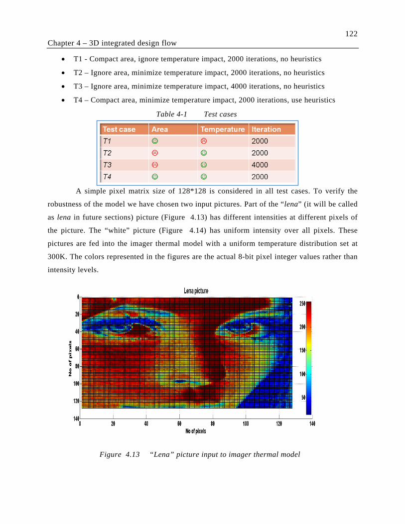
122
Chapter 4 – 3D integrated design flow
• T1 - Compact area, ignore temperature impact, 2000 iterations, no heuristics
• T2 – Ignore area, minimize temperature impact, 2000 iterations, no heuristics
• T3 – Ignore area, minimize temperature impact, 4000 iterations, no heuristics
• T4 – Compact area, minimize temperature impact, 2000 iterations, use heuristics
A simple pixel matrix size of 128*128 is considered in all test cases. To verify the
robustness of the model we have chosen two input pictures. Part of the “lena” (it will be called
as lena in future sections) picture (Figure 4.13) has different intensities at different pixels of
the picture. The “white” picture (Figure 4.14) has uniform intensity over all pixels. These
pictures are fed into the imager thermal model with a uniform temperature distribution set at
300K. The colors represented in the figures are the actual 8-bit pixel integer values rather than
intensity levels.
Table 4-1 Test cases
Figure 4.13 “Lena” picture input to imager thermal model
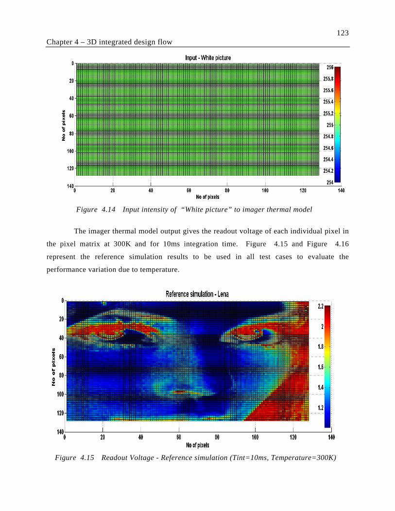
123
Chapter 4 – 3D integrated design flow
The imager thermal model output gives the readout voltage of each individual pixel in
the pixel matrix at 300K and for 10ms integration time. Figure 4.15 and Figure 4.16
represent the reference simulation results to be used in all test cases to evaluate the
performance variation due to temperature.
Figure 4.14 Input intensity of “White picture” to imager thermal model
Figure 4.15 Readout Voltage - Reference simulation (Tint=10ms, Temperature=300K)
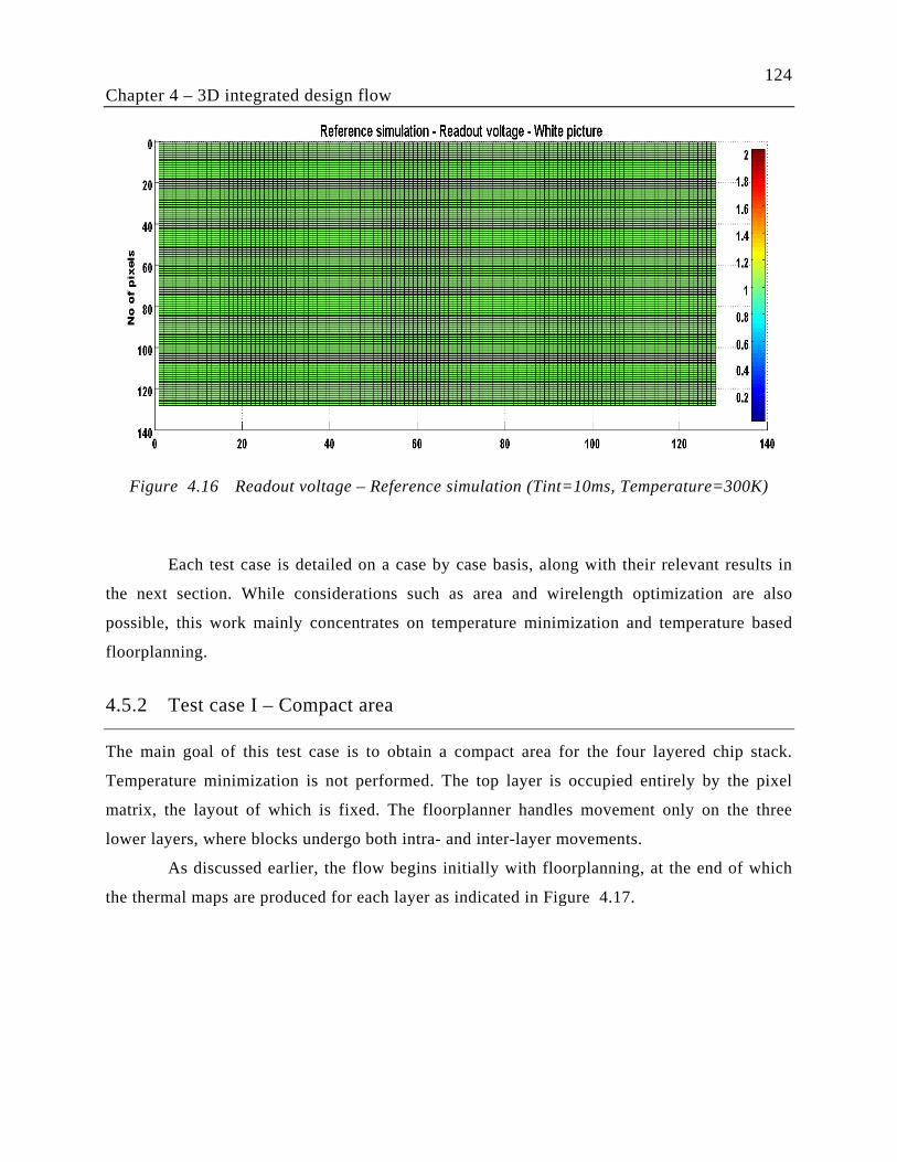
124
Chapter 4 – 3D integrated design flow
Each test case is detailed on a case by case basis, along with their relevant results in
the next section. While considerations such as area and wirelength optimization are also
possible, this work mainly concentrates on temperature minimization and temperature based
floorplanning.
4.5.2 Test case I – Compact area
The main goal of this test case is to obtain a compact area for the four layered chip stack.
Temperature minimization is not performed. The top layer is occupied entirely by the pixel
matrix, the layout of which is fixed. The floorplanner handles movement only on the three
lower layers, where blocks undergo both intra- and inter-layer movements.
As discussed earlier, the flow begins initially with floorplanning, at the end of which
the thermal maps are produced for each layer as indicated in Figure 4.17.
Figure 4.16 Readout voltage – Reference simulation (Tint=10ms, Temperature=300K)
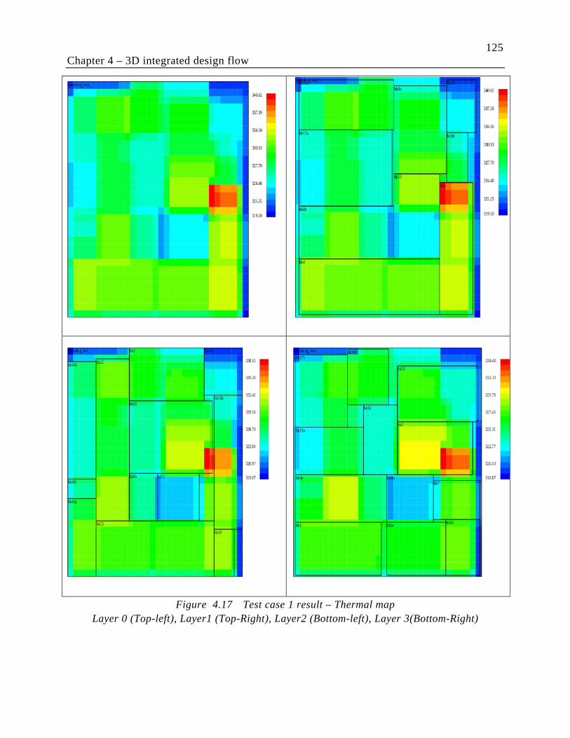
125
Chapter 4 – 3D integrated design flow
Figure 4.17 Test case 1 result – Thermal map Layer 0 (Top-left), Layer1 (Top-Right), Layer2 (Bottom-left), Layer 3(Bottom-Right)
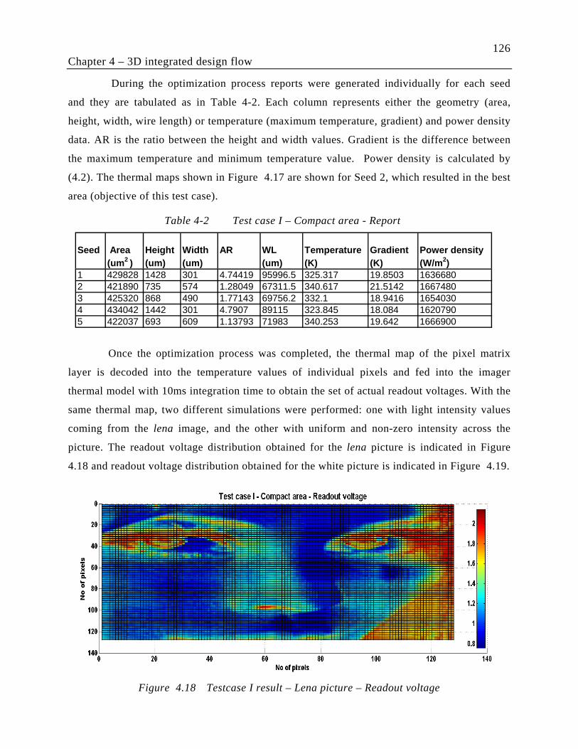
126
Chapter 4 – 3D integrated design flow
During the optimization process reports were generated individually for each seed
and they are tabulated as in Table 4-2. Each column represents either the geometry (area,
height, width, wire length) or temperature (maximum temperature, gradient) and power density
data. AR is the ratio between the height and width values. Gradient is the difference between
the maximum temperature and minimum temperature value. Power density is calculated by
(4.2). The thermal maps shown in Figure 4.17 are shown for Seed 2, which resulted in the best
area (objective of this test case).
Once the optimization process was completed, the thermal map of the pixel matrix
layer is decoded into the temperature values of individual pixels and fed into the imager
thermal model with 10ms integration time to obtain the set of actual readout voltages. With the
same thermal map, two different simulations were performed: one with light intensity values
coming from the lena image, and the other with uniform and non-zero intensity across the
picture. The readout voltage distribution obtained for the lena picture is indicated in Figure
4.18 and readout voltage distribution obtained for the white picture is indicated in Figure 4.19.
Table 4-2 Test case I – Compact area - Report
Figure 4.18 Testcase I result – Lena picture – Readout voltage
Seed Area Height Width AR WL Temperature Gradient Power density(um2 ) (um) (um) (um) (K) (K) (W/m2)
1 429828 1428 301 4.74419 95996.5 325.317 19.8503 16366802 421890 735 574 1.28049 67311.5 340.617 21.5142 16674803 425320 868 490 1.77143 69756.2 332.1 18.9416 16540304 434042 1442 301 4.7907 89115 323.845 18.084 16207905 422037 693 609 1.13793 71983 340.253 19.642 1666900
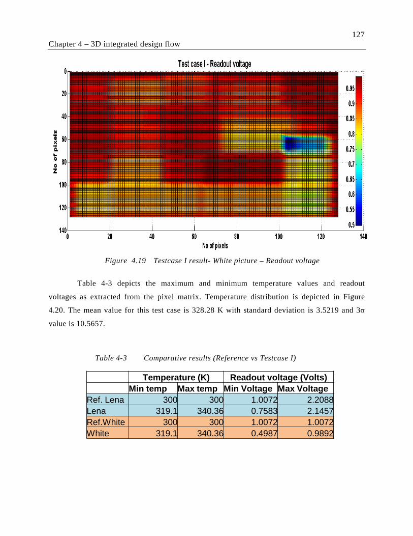
127
Chapter 4 – 3D integrated design flow
Table 4-3 depicts the maximum and minimum temperature values and readout
voltages as extracted from the pixel matrix. Temperature distribution is depicted in Figure
4.20. The mean value for this test case is 328.28 K with standard deviation is 3.5219 and 3σ
value is 10.5657.
Figure 4.19 Testcase I result- White picture – Readout voltage
Temperature (K) Readout voltage (Volts)Min temp Max temp Min Voltage Max Voltage
Ref. Lena 300 300 1.0072 2.2088Lena 319.1 340.36 0.7583 2.1457Ref.White 300 300 1.0072 1.0072White 319.1 340.36 0.4987 0.9892
Table 4-3 Comparative results (Reference vs Testcase I)
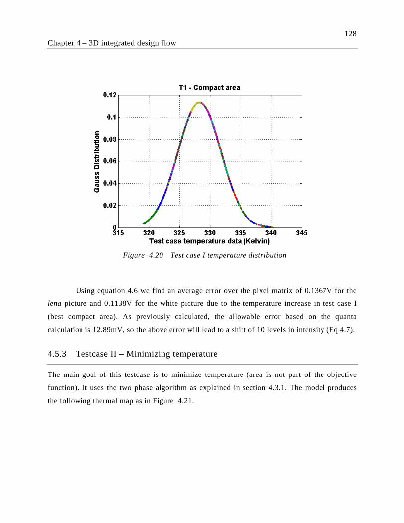
128
Chapter 4 – 3D integrated design flow
Using equation 4.6 we find an average error over the pixel matrix of 0.1367V for the
lena picture and 0.1138V for the white picture due to the temperature increase in test case I
(best compact area). As previously calculated, the allowable error based on the quanta
calculation is 12.89mV, so the above error will lead to a shift of 10 levels in intensity (Eq 4.7).
4.5.3 Testcase II – Minimizing temperature
The main goal of this testcase is to minimize temperature (area is not part of the objective
function). It uses the two phase algorithm as explained in section 4.3.1. The model produces
the following thermal map as in Figure 4.21.
Figure 4.20 Test case I temperature distribution
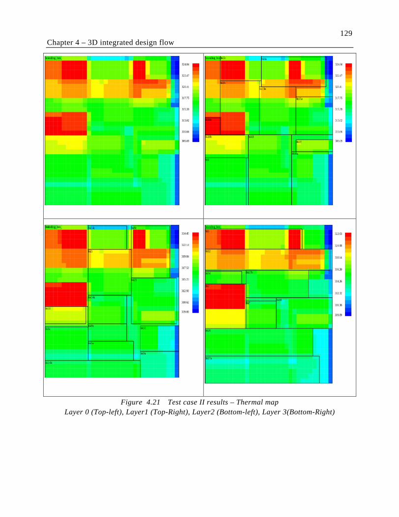
129
Chapter 4 – 3D integrated design flow
Figure 4.21 Test case II results – Thermal map Layer 0 (Top-left), Layer1 (Top-Right), Layer2 (Bottom-left), Layer 3(Bottom-Right)
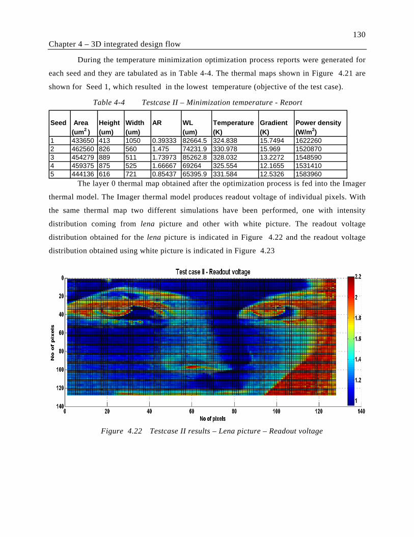
130
Chapter 4 – 3D integrated design flow
During the temperature minimization optimization process reports were generated for
each seed and they are tabulated as in Table 4-4. The thermal maps shown in Figure 4.21 are
shown for Seed 1, which resulted in the lowest temperature (objective of the test case).
The layer 0 thermal map obtained after the optimization process is fed into the Imager
thermal model. The Imager thermal model produces readout voltage of individual pixels. With
the same thermal map two different simulations have been performed, one with intensity
distribution coming from lena picture and other with white picture. The readout voltage
distribution obtained for the lena picture is indicated in Figure 4.22 and the readout voltage
distribution obtained using white picture is indicated in Figure 4.23
Table 4-4 Testcase II – Minimization temperature - Report
Figure 4.22 Testcase II results – Lena picture – Readout voltage
Seed Area Height Width AR WL Temperature Gradient Power density(um2 ) (um) (um) (um) (K) (K) (W/m2)
1 433650 413 1050 0.39333 82664.5 324.838 15.7494 16222602 462560 826 560 1.475 74231.9 330.978 15.969 15208703 454279 889 511 1.73973 85262.8 328.032 13.2272 15485904 459375 875 525 1.66667 69264 325.554 12.1655 15314105 444136 616 721 0.85437 65395.9 331.584 12.5326 1583960
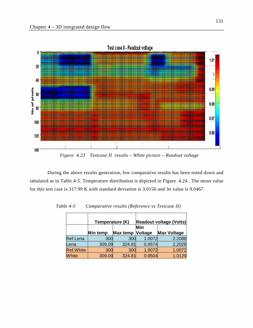
131
Chapter 4 – 3D integrated design flow
During the above results generation, few comparative results has been noted down and
tabulated as in Table 4-5. Temperature distribution is depicted in Figure 4.24 . The mean value
for this test case is 317.99 K with standard deviation is 3.0156 and 3σ value is 9.0467.
Figure 4.23 Testcase II results – White picture – Readout voltage
Temperature (K) Readout voltage (Volts)
Min temp Max tempMin Voltage Max Voltage
Ref.Lena 300 300 1.0072 2.2088Lena 309.09 324.81 0.9574 2.2028Ref.White 300 300 1.0072 1.0072White 309.09 324.81 0.9504 1.0129
Table 4-5 Comparative results (Reference vs Testcase II)
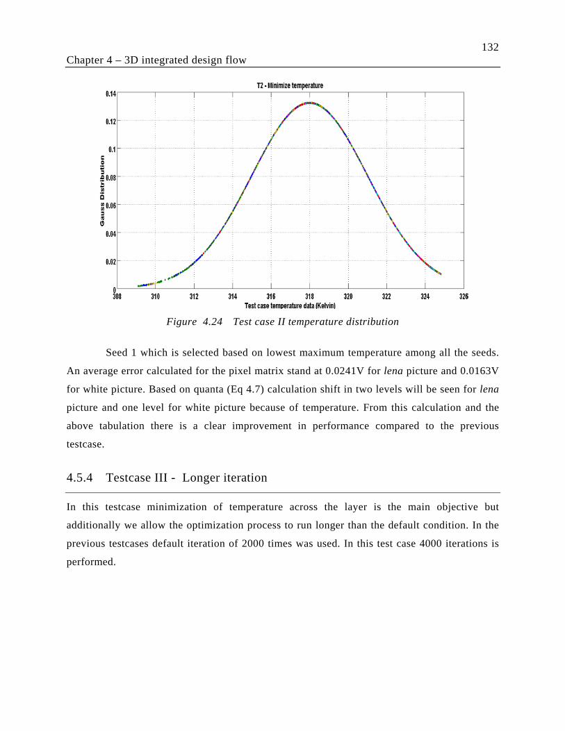
132
Chapter 4 – 3D integrated design flow
Seed 1 which is selected based on lowest maximum temperature among all the seeds.
An average error calculated for the pixel matrix stand at 0.0241V for lena picture and 0.0163V
for white picture. Based on quanta (Eq 4.7) calculation shift in two levels will be seen for lena
picture and one level for white picture because of temperature. From this calculation and the
above tabulation there is a clear improvement in performance compared to the previous
testcase.
4.5.4 Testcase III - Longer iteration
In this testcase minimization of temperature across the layer is the main objective but
additionally we allow the optimization process to run longer than the default condition. In the
previous testcases default iteration of 2000 times was used. In this test case 4000 iterations is
performed.
Figure 4.24 Test case II temperature distribution
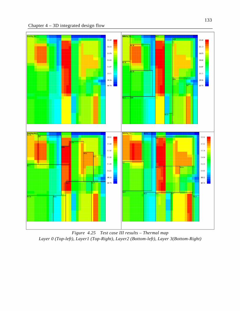
133
Chapter 4 – 3D integrated design flow
Figure 4.25 Test case III results – Thermal map Layer 0 (Top-left), Layer1 (Top-Right), Layer2 (Bottom-left), Layer 3(Bottom-Right)
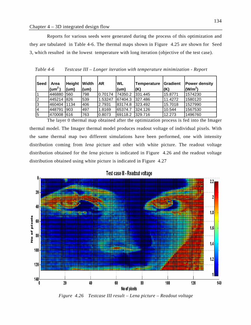
134
Chapter 4 – 3D integrated design flow
Reports for various seeds were generated during the process of this optimization and
they are tabulated in Table 4-6. The thermal maps shown in Figure 4.25 are shown for Seed
3, which resulted in the lowest temperature with long iteration (objective of the test case).
The layer 0 thermal map obtained after the optimization process is fed into the Imager
thermal model. The Imager thermal model produces readout voltage of individual pixels. With
the same thermal map two different simulations have been performed, one with intensity
distribution coming from lena picture and other with white picture. The readout voltage
distribution obtained for the lena picture is indicated in Figure 4.26 and the readout voltage
distribution obtained using white picture is indicated in Figure 4.27
Table 4-6 Testcase III – Longer iteration with temperature minimization - Report
Figure 4.26 Testcase III result – Lena picture – Readout voltage
Seed Area Height Width AR WL Temperature Gradient Power density(um2 ) (um) (um) (um) (K) (K) (W/m2)
1 446880 560 798 0.70174 74350.2 331.445 15.8771 15742302 445214 826 539 1.53247 67404.3 327.486 11.4272 15801203 460404 1134 406 2.7931 83174.8 323.492 15.7018 15279904 448791 903 497 1.8169 65374.7 324.126 10.544 15675305 470008 616 763 0.8073 69118.2 329.716 12.273 1496760
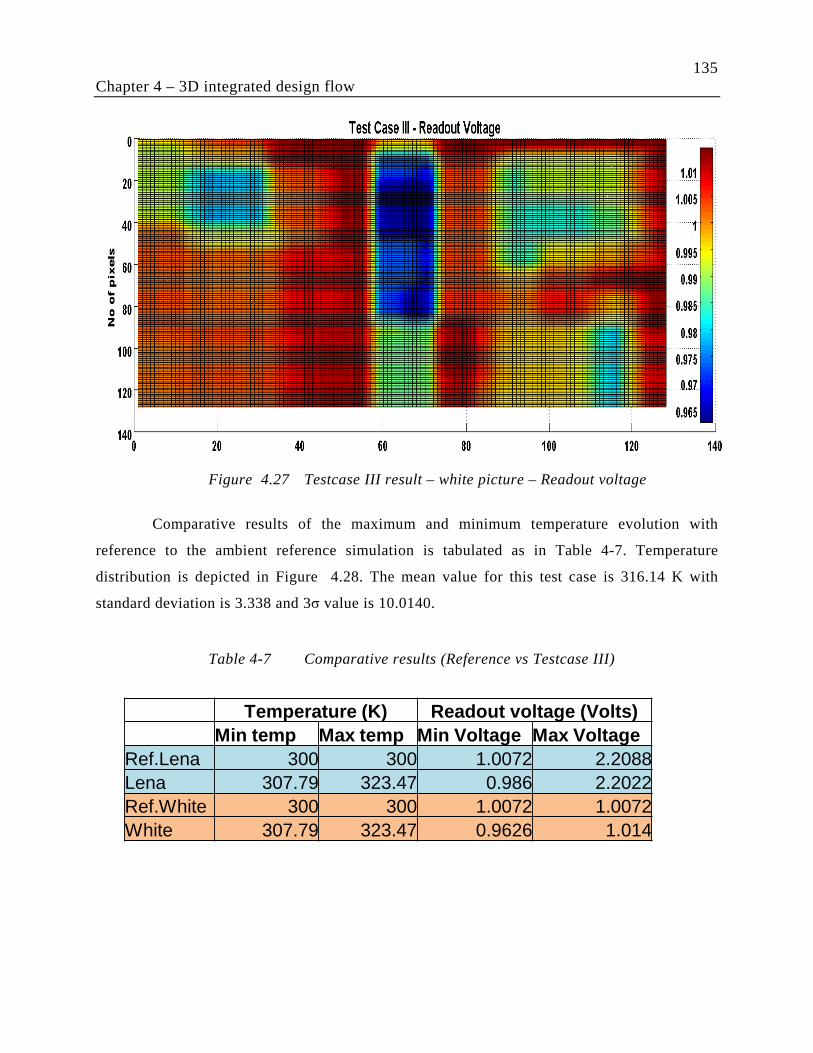
135
Chapter 4 – 3D integrated design flow
Comparative results of the maximum and minimum temperature evolution with
reference to the ambient reference simulation is tabulated as in Table 4-7. Temperature
distribution is depicted in Figure 4.28. The mean value for this test case is 316.14 K with
standard deviation is 3.338 and 3σ value is 10.0140.
Figure 4.27 Testcase III result – white picture – Readout voltage
Temperature (K) Readout voltage (Volts)Min temp Max temp Min Voltage Max Voltage
Ref.Lena 300 300 1.0072 2.2088Lena 307.79 323.47 0.986 2.2022Ref.White 300 300 1.0072 1.0072White 307.79 323.47 0.9626 1.014
Table 4-7 Comparative results (Reference vs Testcase III)
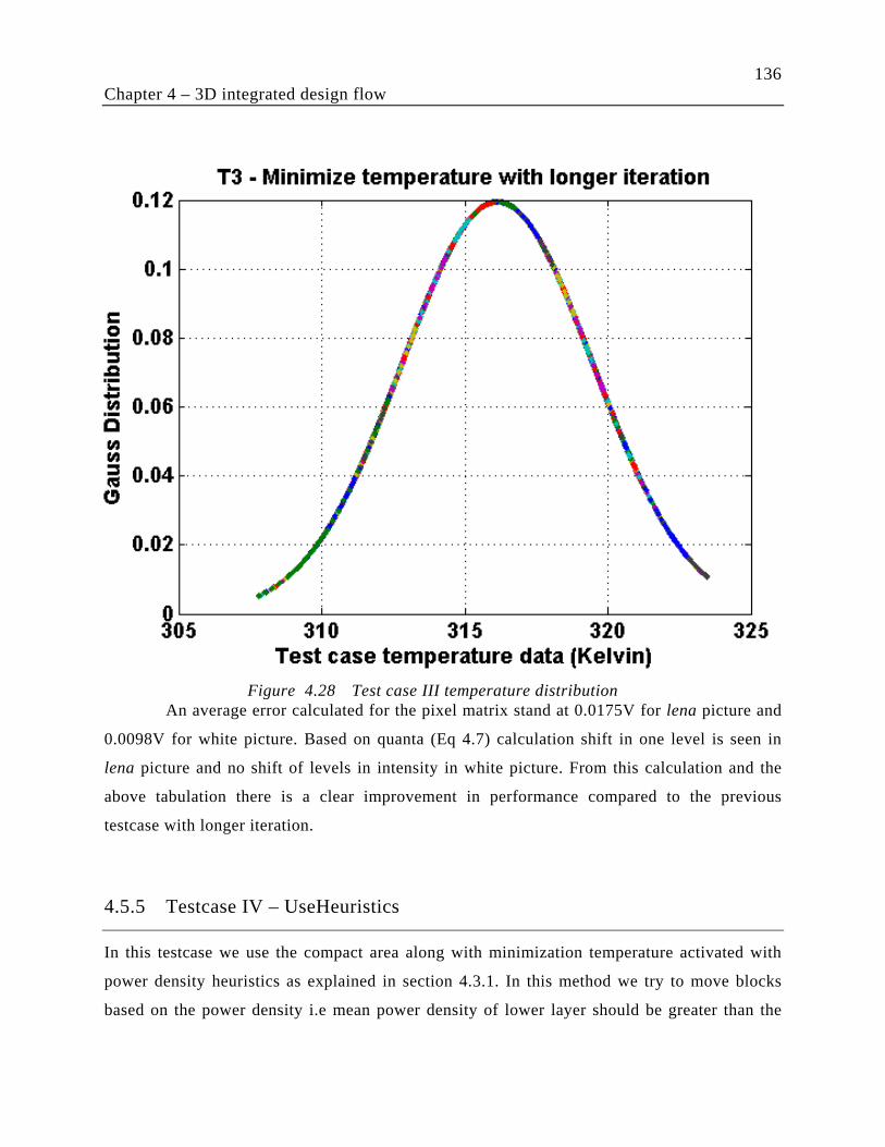
136
Chapter 4 – 3D integrated design flow
An average error calculated for the pixel matrix stand at 0.0175V for lena picture and
0.0098V for white picture. Based on quanta (Eq 4.7) calculation shift in one level is seen in
lena picture and no shift of levels in intensity in white picture. From this calculation and the
above tabulation there is a clear improvement in performance compared to the previous
testcase with longer iteration.
4.5.5 Testcase IV – UseHeuristics
In this testcase we use the compact area along with minimization temperature activated with
power density heuristics as explained in section 4.3.1. In this method we try to move blocks
based on the power density i.e mean power density of lower layer should be greater than the
Figure 4.28 Test case III temperature distribution
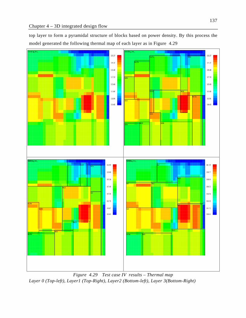
137
Chapter 4 – 3D integrated design flow
top layer to form a pyramidal structure of blocks based on power density. By this process the
model generated the following thermal map of each layer as in Figure 4.29
Figure 4.29 Test case IV results – Thermal map Layer 0 (Top-left), Layer1 (Top-Right), Layer2 (Bottom-left), Layer 3(Bottom-Right)
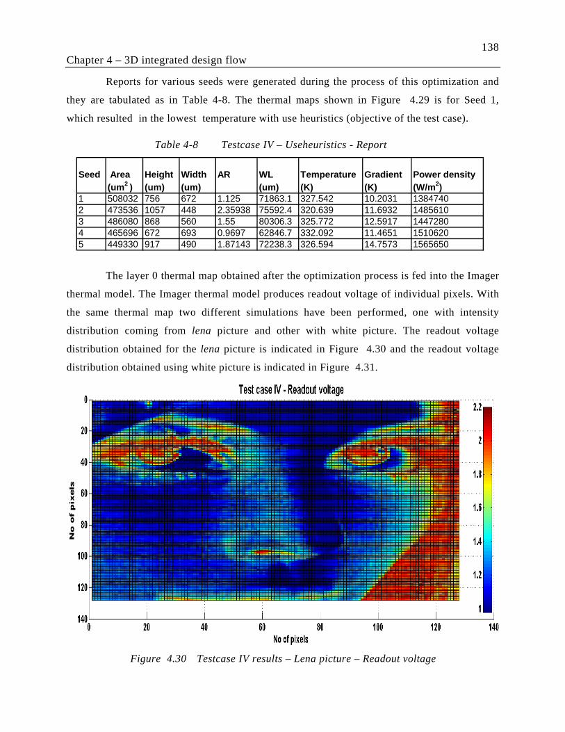
138
Chapter 4 – 3D integrated design flow
Reports for various seeds were generated during the process of this optimization and
they are tabulated as in Table 4-8. The thermal maps shown in Figure 4.29 is for Seed 1,
which resulted in the lowest temperature with use heuristics (objective of the test case).
The layer 0 thermal map obtained after the optimization process is fed into the Imager
thermal model. The Imager thermal model produces readout voltage of individual pixels. With
the same thermal map two different simulations have been performed, one with intensity
distribution coming from lena picture and other with white picture. The readout voltage
distribution obtained for the lena picture is indicated in Figure 4.30 and the readout voltage
distribution obtained using white picture is indicated in Figure 4.31.
Table 4-8 Testcase IV – Useheuristics - Report
Figure 4.30 Testcase IV results – Lena picture – Readout voltage
Seed Area Height Width AR WL Temperature Gradient Power density(um2 ) (um) (um) (um) (K) (K) (W/m2)
1 508032 756 672 1.125 71863.1 327.542 10.2031 13847402 473536 1057 448 2.35938 75592.4 320.639 11.6932 14856103 486080 868 560 1.55 80306.3 325.772 12.5917 14472804 465696 672 693 0.9697 62846.7 332.092 11.4651 15106205 449330 917 490 1.87143 72238.3 326.594 14.7573 1565650
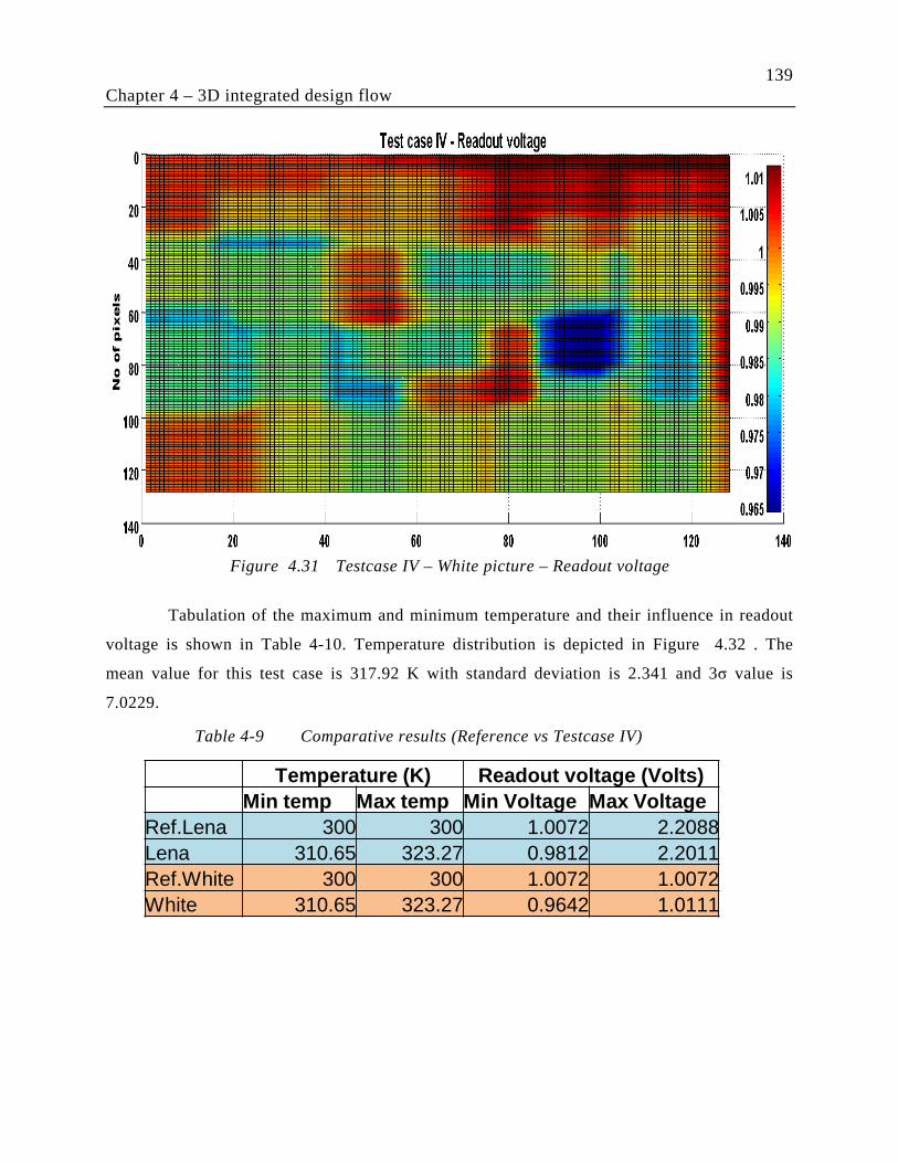
139
Chapter 4 – 3D integrated design flow
Tabulation of the maximum and minimum temperature and their influence in readout
voltage is shown in Table 4-10. Temperature distribution is depicted in Figure 4.32 . The
mean value for this test case is 317.92 K with standard deviation is 2.341 and 3σ value is
7.0229.
Figure 4.31 Testcase IV – White picture – Readout voltage
Temperature (K) Readout voltage (Volts)Min temp Max temp Min Voltage Max Voltage
Ref.Lena 300 300 1.0072 2.2088Lena 310.65 323.27 0.9812 2.2011Ref.White 300 300 1.0072 1.0072White 310.65 323.27 0.9642 1.0111
Table 4-9 Comparative results (Reference vs Testcase IV)
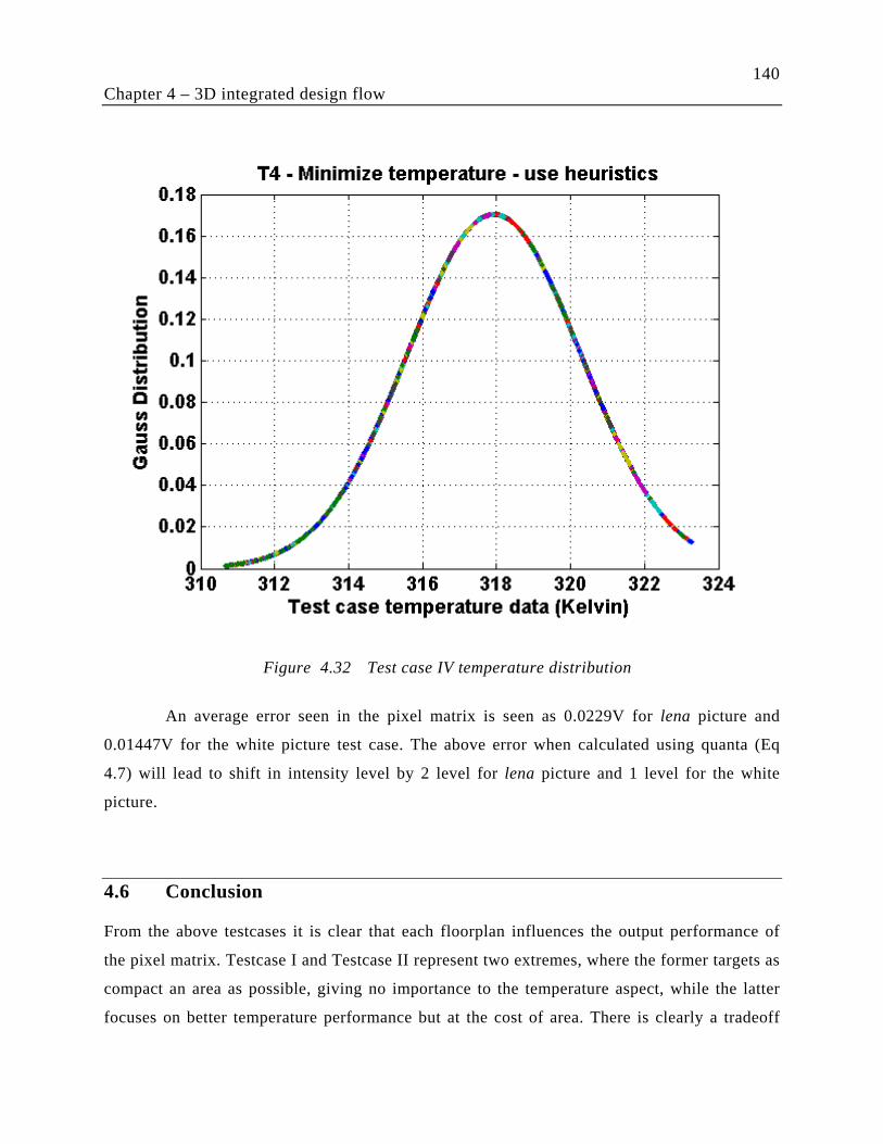
140
Chapter 4 – 3D integrated design flow
An average error seen in the pixel matrix is seen as 0.0229V for lena picture and
0.01447V for the white picture test case. The above error when calculated using quanta (Eq
4.7) will lead to shift in intensity level by 2 level for lena picture and 1 level for the white
picture.
4.6 Conclusion From the above testcases it is clear that each floorplan influences the output performance of
the pixel matrix. Testcase I and Testcase II represent two extremes, where the former targets as
compact an area as possible, giving no importance to the temperature aspect, while the latter
focuses on better temperature performance but at the cost of area. There is clearly a tradeoff
Figure 4.32 Test case IV temperature distribution
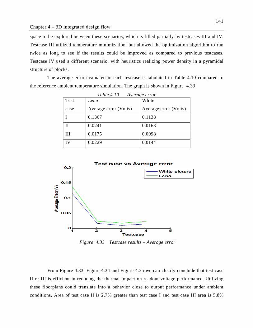
141
Chapter 4 – 3D integrated design flow
space to be explored between these scenarios, which is filled partially by testcases III and IV.
Testcase III utilized temperature minimization, but allowed the optimization algorithm to run
twice as long to see if the results could be improved as compared to previous testcases.
Testcase IV used a different scenario, with heuristics realizing power density in a pyramidal
structure of blocks.
The average error evaluated in each testcase is tabulated in Table 4.10 compared to
the reference ambient temperature simulation. The graph is shown in Figure 4.33
Table 4.10 Average error Test
case
Lena
Average error (Volts)
White
Average error (Volts)
I 0.1367 0.1138
II 0.0241 0.0163
III 0.0175 0.0098
IV 0.0229 0.0144
From Figure 4.33, Figure 4.34 and Figure 4.35 we can clearly conclude that test case
II or III is efficient in reducing the thermal impact on readout voltage performance. Utilizing
these floorplans could translate into a behavior close to output performance under ambient
conditions. Area of test case II is 2.7% greater than test case I and test case III area is 5.8%
Figure 4.33 Testcase results – Average error
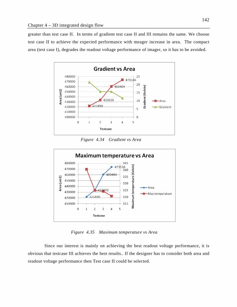
142
Chapter 4 – 3D integrated design flow
greater than test case II. In terms of gradient test case II and III remains the same. We choose
test case II to achieve the expected performance with meager increase in area. The compact
area (test case I), degrades the readout voltage performance of imager, so it has to be avoided.
Since our interest is mainly on achieving the best readout voltage performance, it is
obvious that testcase III achieves the best results.. If the designer has to consider both area and
readout voltage performance then Test case II could be selected.
Figure 4.34 Gradient vs Area
Figure 4.35 Maximum temperature vs Area

143
Chapter 4 – 3D integrated design flow
Thus the complete 3D integrated design flow is realized with the following
• 3D Integrated design flow integrating
• Floorplanner
o 3D stacked layers
o Flexible integration of block information
• Thermal simulation
o Flexibility in adding material properties
o Accurate and fast thermal simulation
• Imager simulation
o Readout voltage = f (Temperature, Light , Integration time)
o Accurate results
o High speed simulation
This design environment could handle any size of pixel matrix, and groups together
floorplanning and thermal simulation, which is missing from existing industrial design flows.
The procedure followed in this work could be easily followed to utilize the capability of the
model to realize an imager which will meet the performance requirement at early stages of
design space exploration. Moving to 3D stacked Imager IC could also be met with this work.
144
Chapter 4 – 3D integrated design flow
Bibliography
[1] Meindl, J.D. et al,” Beyond Moore's law: the interconnect era.” Computing in science and engineering, Feb 2003. Vol.5,no.1,p20-24.
[2] R.S.Patti. et al,” Three dimensional integrated circuites and the future of System on chip designs”. : Proceedings of the IEEE, June 2006. 94, p1214-24.
[3] S.Tiwar, H.S.Kim et al,”Three dimensional integration in silicon electronics”. :Proceedings IEEE Lester Eastman Conference on High performance Devices, 2002. p24-33.
[4] W.Davis, E.Oh et al,” Application exploration for 3-d integrated circuits: Tcam, fifo, and fft case studies”. VLSI systems, IEEE Transctions, April 2009. Vol 17, no.4, pp496-506.
[5] W.Huang, M.Stan et al, ”Interaction of scaling trends in processor architecture and cooling.” Semi-therm, Feb 2010. pp.198-204.
[6] F.Frantz, L.Labrak, I.O'Connor,”3D IC Floorplanning: Automating optimization setting and exploring new thermal-aware management techniques”.: Microelectronics journal, June 2012, Vol. 43. Page 423-432, ISSN 0026-2692.
[7] S.Adya, I.Markov et al,” Fixed-outline floorplanning: enabling hierarchical design”. VLSI systems, IEEE Transaction, Dec 2003, Vol. 11. pp.1120-1135.
[8] F.Frantz,” Multi objective 3D floorplanner.” INL internal report, October 2010.
[9] K.Skadron, K.Sankaranarayanana, S.Velusamy, D.Tarjan, M.R.Stan and W.Huang,“Temperature-Aware Microarchitecture: Modeling and Implementation.” March 2004, ACM Transactions on Architecture and Code Optimization, pp. 1(1):94-125.
[10] J.Cong, J.Wei,Y.Zhang et al, ” A thermal- driven floorplanning for 3D ICs”: ICCAD. IEEE Computer Society / ACM, 2004. pp. 306–313.

145
Chapter 4 – 3D integrated design flow
[11] L. Xiao, S. Sinha, J. Xu, and E. Young et al, “Fixed-outline thermal-aware 3d floorplanning.” ASP-DAC, Jan 2010. pp 561-567.
[12] S.Mendis, S.E.Kemeny, E.Fossum et al, [Online], Bookshelf format. http://vlsicad.eecs.umich.edu/BK/.
[13] The MCNC Benchmark Problems for VLSI Floorplanning [online]. Available http://www.mcnc.org
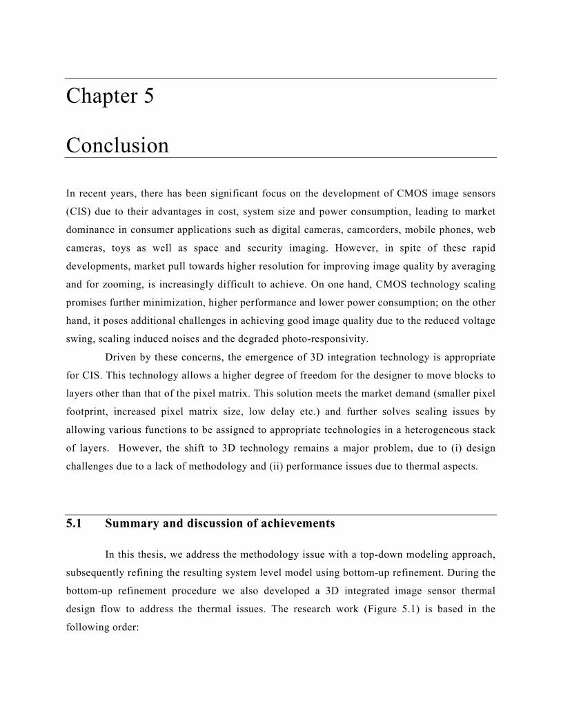
Chapter 5 Conclusion
In recent years, there has been significant focus on the development of CMOS image sensors
(CIS) due to their advantages in cost, system size and power consumption, leading to market
dominance in consumer applications such as digital cameras, camcorders, mobile phones, web
cameras, toys as well as space and security imaging. However, in spite of these rapid
developments, market pull towards higher resolution for improving image quality by averaging
and for zooming, is increasingly difficult to achieve. On one hand, CMOS technology scaling
promises further minimization, higher performance and lower power consumption; on the other
hand, it poses additional challenges in achieving good image quality due to the reduced voltage
swing, scaling induced noises and the degraded photo-responsivity.
Driven by these concerns, the emergence of 3D integration technology is appropriate
for CIS. This technology allows a higher degree of freedom for the designer to move blocks to
layers other than that of the pixel matrix. This solution meets the market demand (smaller pixel
footprint, increased pixel matrix size, low delay etc.) and further solves scaling issues by
allowing various functions to be assigned to appropriate technologies in a heterogeneous stack
of layers. However, the shift to 3D technology remains a major problem, due to (i) design
challenges due to a lack of methodology and (ii) performance issues due to thermal aspects.
5.1 Summary and discussion of achievements
In this thesis, we address the methodology issue with a top-down modeling approach,
subsequently refining the resulting system level model using bottom-up refinement. During the
bottom-up refinement procedure we also developed a 3D integrated image sensor thermal
design flow to address the thermal issues. The research work (Figure 5.1) is based in the
following order:
147
Chapter 5 – Conclusion
• Top-down design methodology
• Bottom-Up refinement
o Image sensor thermal model
• 3D integrated thermal design flow
Top-down design methodology
In this part of the work, we developed flexible models supporting a top-down (TD) design
methodology. Models are developed at different abstraction levels in a TD approach in order to
analyze the system and for synthesizing the system. These models are optimized with respect
to the intended functionality and help in the early stages of design space exploration.
We focused our research work specifically on the pixel matrix and ADC block to
prove the hierarchical modeling approach. During this work we formulated the TD approach
based on parameter dependency graphs and segregated all the performance/parameter pairs into
abstraction levels. The models developed are optimized and can be tuned according to the
changes in the system performance requirements. All the models developed from system level
down to the lower levels respected the system specifications.
System
System level
Behavioral
level
Accurate
behavioral
level
Top
-d
ow
n
Electrical
schematic
simulation
Bo
tto
m-u
p r
efi
ne
me
nt
3D Integrated design flow
Imager thermal
model
HotSpot
3D
Floorplanner
Tools
Figure 5.1 High level flow diagram

148
Chapter 5 – Conclusion
In the top-down design methodology the propagation to each lower level respected a
system level performance value. To explore the overall system performance we extended our
work with a Pareto-front methodology.
Pareto-front methodology
The drawback of the top-down approach is that the derived requirements may not be feasible
(for the available technology). To overcome this limitation, we used the Pareto-front
methodology to perform
• Exploration of the entire design space at system level
• Inclusion of limitations at lower levels into system-level design space
• Easy visualization of the tradeoff between various performances
This methodology was successfully proved using the pixel matrix block and we
computed the Pareto-front of the pixel matrix design.
Bottom-up refinement
In the top-down approach, the models utilized the ambient (300K) temperature condition.
Moving to a 3D stacked IC required a detailed study on the thermal issues and refinement of
the system level model using the data extracted from the transistor level to evaluate the system
performance degradation due to temperature. This refinement step is used in system validation
or system exploration.
Image sensor thermal model
The image sensor thermal model was developed using the following steps:
• Electrical simulation
Exhaustive data generation using electrical simulation is performed covering the full range
of operation of the imager.
• Modeling based on surface fitting methodology
Firstly, realized simple model fitting was carried out with the data obtained from the
electrical simulation using two independent variables (temperature and light intensity) to
prove the methodology. The work was subsequently extended to volume fitting with three
independent variables (temperature, light intensity and integration time) to cover the entire
range of operation of image sensor. A pre-validation step was performed to validate the
model at random values of temperature and integration time to select the lowest order of
fitting capable of achieveing the desired accuracy.
149
Chapter 5 – Conclusion
• SystemC Model
A scalable SystemC based pixel matrix module was developed with an image processing
toolbox to decode a picture and convert it into light intensity values. It is also equipped
with thermal map reading/writing features. After these initial tool development steps, the
pre-validated model was integrated into the SystemC environment to output the readout
voltage as a function of temperature, light intensity and integration time. In the current
form, the model can simulate from third to sixth order of fitting.
• Tradeoff analysis
After integration of the fitted model into SystemC, we performed a post-validation
step to analyze the simulation time with respect to various orders of fitting. This part of the
work clearly pointed out the tradeoff between simulation time and accuracy. For example:
simulation time of 256*256 pixel matrix is 240ms (third order fitting) with relative error of
under 1.047% compared to 630ms simulation time (sixth order fitting) with relative error of
0.042%.
• Validation
An extensive validation step was performed to prove the robustness of the model with
128*128 and 256*256 pixel lena pictures. Furthermore, it was also validated with a
uniform (white) picture at 350K temperature to prove the reliability of this model even in
extreme (bright light) system operating condition.
• Simulation time
Finally, the model was used to simulate at the system level. A first conclusion is that the
model has a good simulation speed-up (500,000X) compared to conventional simulation
performed using Spice-based simulators at the electrical level. It also adheres to the
accuracy criterion (relative error of 4% in 256*256 pixel matrix size) to ensure no change
in the intensity level at the output. This model can simulate accurately at system level and
take into account inter-pixel variability.
The image sensor thermal model has the capacity to simulate accurately with low
simulation time, but used in the initial development a homogeneous temperature
distribution. To solve this issue, a 3D integrated thermal design flow was realized with the
following features.

150
Chapter 5 – Conclusion
3D-Integrated thermal design flow
A 3D integrated thermal design flow was realized in order to couple the thermal map generated
from this model as an input to the thermal-aware imager model. The 3D integrated thermal
design flow was also used in the design cycle to help adjust the placement of blocks in
underlying layers according to their power density and in order to minimize their impact on the
imager performance.
This design flow integrated a 3D floorplanner (Parquet) and a thermal simulator
(HotSpot) to explore the use of many layers in a 3D stacked imager to support greater freedom
of movement. This movement is to enable the movement of high-power blocks away from
temperature-sensitive areas or layers in the final placement. At the end of this placement, we
generate the thermal map of each layer of the chip.
This generated thermal map is utilized in the image sensor thermal model to simulate
the realistic behavior of the imager. This work has been validated with several test cases
showing the importance of different scenarios and their impact on imager performance. At the
end of this work a tradeoff between area and temperature impact was studied.
Thus this research work has accomplished a hierarchical design approach with an
imager as application. As part of the bottom-up refinement, a detailed study of the thermal
impact on the imager performance was made along with the development of a fast image
sensor thermal simulator.
5.2 Future perspectives
In general, the presented work and results show the feasibility of the top-down approach and
further improvements using bottom-up refinement. This does not mean the work is complete.
There remains much to be resolved and included in the modeling and design aspects. First and
foremost is running the synthesis cycle for different technologies and for different blocks in
order to apply the approach more globally. All through this work, AMS 0.35µm is used.
Further extension in the models is necessary in case different technologies are utilized. Pareto-
front methodology is realized only for the pixel matrix. This work can be extended to the
complete system.

151
Chapter 5 – Conclusion
In this work, only a 3T-APS architecture is used to prove our methodology. Future
work is necessary to realize different architectures such as 4T, 2.5T, 1.75T and 1.5T APS.
Detailed study on readout circuitry, blooming, cross-talk, variability of process parameters
specific to imagers is necessary. This work mainly concentrated on the pixel matrix and ADC -
other blocks such as CDS, column amplifier and ISP can be modeled.
The image sensor thermal model was developed with a fixed sizing of all three
transistors and the photodiode. The model can be extended in terms of variable transistor sizing
as function of temperature. Developing such a system-level model will be very useful to
analyze performance improvements along with thermal aspects. The existing model can be
improved to study High Dynamic Range (HDR) imaging at the system level. Since the model
has low simulation time, it can act as a good starting point to analyze the behavior of output
image when we combine several images taken at both low light and bright light condition. This
model can also be used to realize software-based localized corrections near the region of high
temperature. Furthermore this model can be scaled to higher than 8 bits resolution of ADC.
According to the thermal model accuracy we have the model could be scaled upto 12 bits
(quanta of 552µV). Moving to higher order of fitting can be investigated to realize 14 bits
resolution.
With respect to the 3D integrated thermal design flow, the work has been validated
only with ami33 benchmark. It can be validated with other benchmarks, and can further be
realized with temperature values measured from a real prototype or with a realistic imager
floorplan. Automating the floorplanner flow, HotSpot simulation integrated with the imager
sensor thermal model is necessary. In the current state, the best floorplan is chosen manually.
This can be extended by automating the design flow to run all the design scenarios to choose
the best scenario.
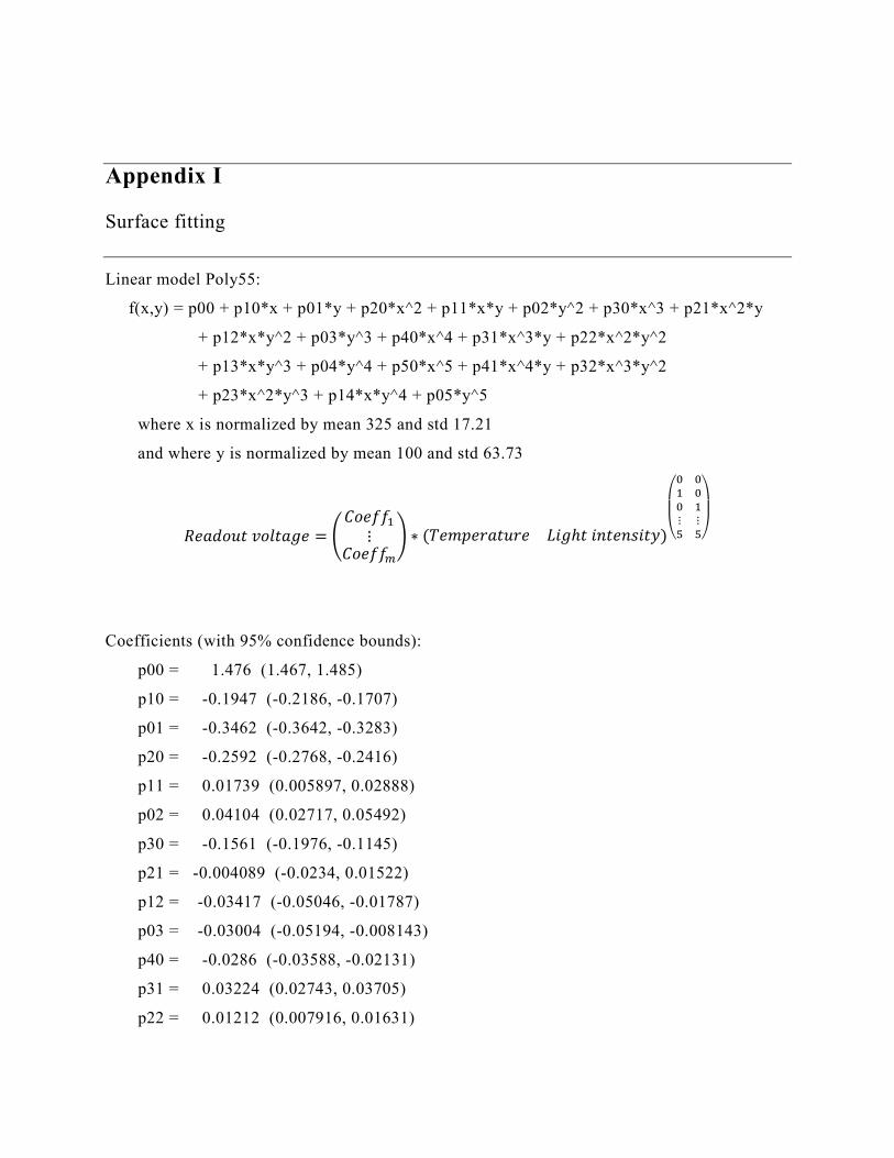
Appendix I
Surface fitting
Linear model Poly55:
f(x,y) = p00 + p10*x + p01*y + p20*x^2 + p11*x*y + p02*y^2 + p30*x^3 + p21*x^2*y
+ p12*x*y^2 + p03*y^3 + p40*x^4 + p31*x^3*y + p22*x^2*y^2
+ p13*x*y^3 + p04*y^4 + p50*x^5 + p41*x^4*y + p32*x^3*y^2
+ p23*x^2*y^3 + p14*x*y^4 + p05*y^5
where x is normalized by mean 325 and std 17.21
and where y is normalized by mean 100 and std 63.73
= ⋮ ∗ ℎ !
"#$ $ $$ ⋮ ⋮% %&
'(
Coefficients (with 95% confidence bounds):
p00 = 1.476 (1.467, 1.485)
p10 = -0.1947 (-0.2186, -0.1707)
p01 = -0.3462 (-0.3642, -0.3283)
p20 = -0.2592 (-0.2768, -0.2416)
p11 = 0.01739 (0.005897, 0.02888)
p02 = 0.04104 (0.02717, 0.05492)
p30 = -0.1561 (-0.1976, -0.1145)
p21 = -0.004089 (-0.0234, 0.01522)
p12 = -0.03417 (-0.05046, -0.01787)
p03 = -0.03004 (-0.05194, -0.008143)
p40 = -0.0286 (-0.03588, -0.02131)
p31 = 0.03224 (0.02743, 0.03705)
p22 = 0.01212 (0.007916, 0.01631)
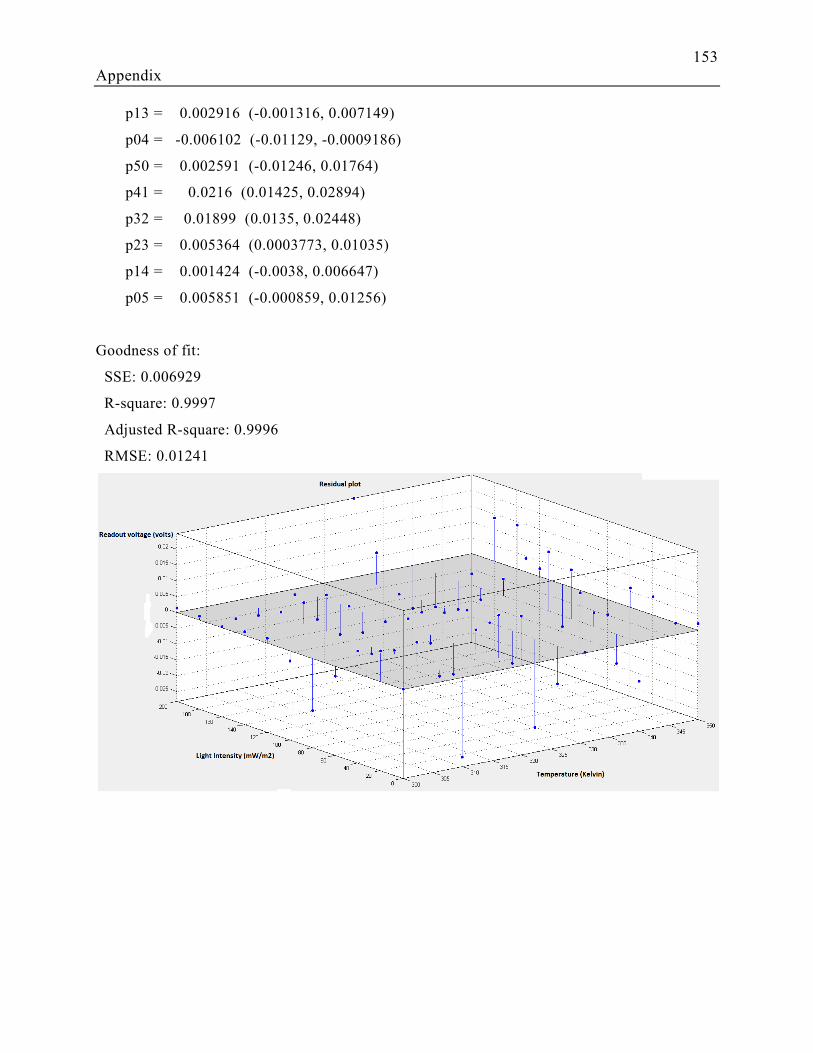
153
Appendix
p13 = 0.002916 (-0.001316, 0.007149)
p04 = -0.006102 (-0.01129, -0.0009186)
p50 = 0.002591 (-0.01246, 0.01764)
p41 = 0.0216 (0.01425, 0.02894)
p32 = 0.01899 (0.0135, 0.02448)
p23 = 0.005364 (0.0003773, 0.01035)
p14 = 0.001424 (-0.0038, 0.006647)
p05 = 0.005851 (-0.000859, 0.01256)
Goodness of fit:
SSE: 0.006929
R-square: 0.9997
Adjusted R-square: 0.9996
RMSE: 0.01241

154
Appendix
Appendix II
Volume fitting
%% Reshape data for fitting.
% Y vector is the voltage as column.
%To model photo diode discharge voltage output
%Y = [ photoout10ms(:); photoout8ms(:); photoout6ms(:); photoout4ms(:); photoout2ms(:) ];
%To model pixel readout voltage
Y = [ readout10ms(:); readout8ms(:); readout6ms(:); readout4ms(:); readout2ms(:)];
% X vector is [ Tint, Light, Temp ].
NSamples = numel( photoout10ms );
X(:,1) = [ 10*ones( NSamples, 1 ); 8*ones( NSamples, 1 ); 6*ones( NSamples, 1 ); 4*ones(
NSamples, 1 ); 2*ones( NSamples, 1 ) ];
l = 1;
for k=1:5
for i=1:length(Light)
for j=1:(length(Temperature))
X(l,2) = Light(i);
X(l,3) = Temperature(j);
l=l+1;
end
end
end
%% Filter out the points that are too low.
THRESHOLD = 0.1;
X( Y < THRESHOLD, : ) = [];
Y( Y < THRESHOLD ) = [];
%% Try a polynomial fit.
path( path, 'runePoly' );
% Dimensions of the problem.
NVAR = size( X, 2 );
NORDER = 6; %order of the fitting
% Call the function to fit a polynomial.
[ polyCoeff, output, XPS, YPS ] = doFittingIteration( NORDER, X, Y );
% Get the function to evaluate the polynomial.
[ hPolyEval, ~, ~, ~, orderMatrix ] = getEvaluationFunction( NORDER, NVAR );
%% Do some plots.
Tint = linspace( 2, 10, 5 );
NGRID = 30;
for i=1:length( Tint )
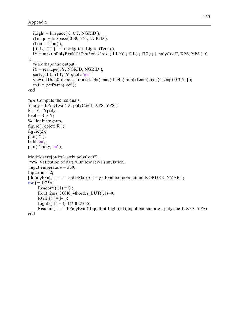
155
Appendix
iLight = linspace( 0, 0.2, NGRID );
iTemp = linspace( 300, 370, NGRID );
iTint = Tint(i);
[ iLL, iTT ] = meshgrid( iLight, iTemp );
iY = max( hPolyEval( [ iTint*ones( size(iLL(:)) ) iLL(:) iTT(:) ], polyCoeff, XPS, YPS ), 0
);
% Reshape the output.
iY = reshape( iY, NGRID, NGRID );
surfc( iLL, iTT, iY );hold 'on'
view( 116, 20 ); axis( [ min(iLight) max(iLight) min(iTemp) max(iTemp) 0 3.5 ] );
fr(i) = getframe( gcf );
end
%% Compute the residuals.
Ypoly = hPolyEval( X, polyCoeff, XPS, YPS );
R = Y - Ypoly;
Rrel = R ./ Y;
% Plot histogram.
figure(1);plot( R );
figure(2);
plot( Y );
hold 'on';
plot( Ypoly, 'm' );
Modeldata=[orderMatrix polyCoeff];
%% Validation of data with low level simulation.
Inputtemperature = 300;
Inputtint = 2;
[ hPolyEval, ~, ~, ~, orderMatrix ] = getEvaluationFunction( NORDER, NVAR );
for j = 1:256
Readout (j,1) = 0 ;
Rout_2ms_300K_4thorder_LUT(j,1)=0;
RGB(j,1)=(j-1);
Light (j,1) = (j-1)* 0.2/255;
Readout(j,1) = hPolyEval([Inputtint,Light(j,1),Inputtemperature], polyCoeff, XPS, YPS)
end
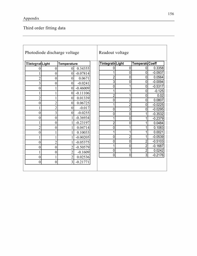
156
Appendix
Third order fitting data
Photodiode discharge voltage Readout voltage
TintegrationLight Temperature
0 0 0 0.34355
1 0 0 -0.07814
2 0 0 0.0671
3 0 0 -0.0241
0 1 0 -0.46009
1 1 0 -0.11106
2 1 0 0.01339
0 2 0 0.06725
1 2 0 -0.017
0 3 0 -0.0255
0 0 1 -0.36934
1 0 1 -0.23197
2 0 1 0.04714
0 1 1 0.10033
1 1 1 -0.00205
0 2 1 -0.05375
0 0 2 -0.50579
1 0 2 -0.1609
0 1 2 0.02536
0 0 3 -0.21771
TintegrationLight TemperatureCoeff
0 0 0 0.3358
1 0 0 -0.0937
2 0 0 0.0564
3 0 0 -0.0094
0 1 0 -0.5317
1 1 0 -0.125
2 1 0 0.02
0 2 0 0.0807
1 2 0 -0.0225
0 3 0 -0.0295
0 0 1 -0.3532
1 0 1 -0.2379
2 0 1 0.0484
0 1 1 0.1083
1 1 1 0.0021
0 2 1 -0.0539
0 0 2 -0.5103
1 0 2 -0.1687
0 1 2 0.0242
0 0 3 -0.2176
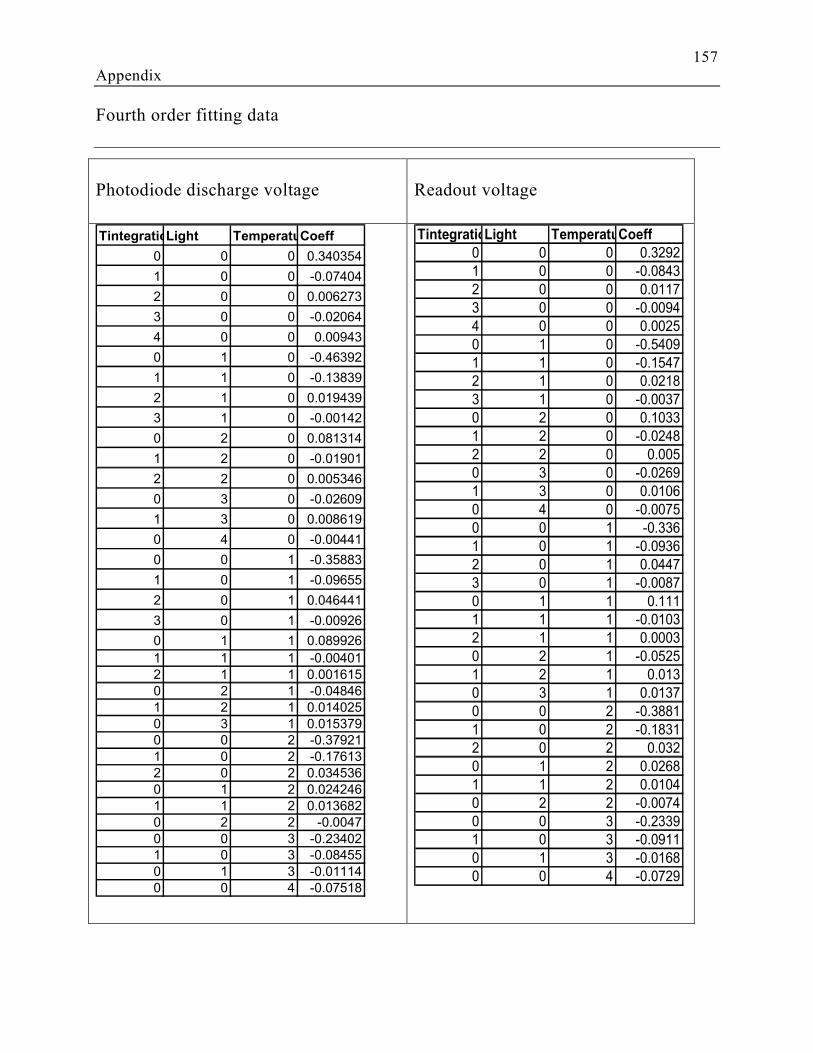
157
Appendix
Fourth order fitting data
Photodiode discharge voltage Readout voltage
TintegrationLight TemperatureCoeff
0 0 0 0.3292
1 0 0 -0.0843
2 0 0 0.0117
3 0 0 -0.0094
4 0 0 0.0025
0 1 0 -0.5409
1 1 0 -0.1547
2 1 0 0.0218
3 1 0 -0.0037
0 2 0 0.1033
1 2 0 -0.0248
2 2 0 0.005
0 3 0 -0.0269
1 3 0 0.0106
0 4 0 -0.0075
0 0 1 -0.336
1 0 1 -0.0936
2 0 1 0.0447
3 0 1 -0.0087
0 1 1 0.111
1 1 1 -0.0103
2 1 1 0.0003
0 2 1 -0.0525
1 2 1 0.013
0 3 1 0.0137
0 0 2 -0.3881
1 0 2 -0.1831
2 0 2 0.032
0 1 2 0.0268
1 1 2 0.0104
0 2 2 -0.0074
0 0 3 -0.2339
1 0 3 -0.0911
0 1 3 -0.0168
0 0 4 -0.0729
TintegrationLight TemperatureCoeff
0 0 0 0.340354
1 0 0 -0.07404
2 0 0 0.006273
3 0 0 -0.02064
4 0 0 0.00943
0 1 0 -0.46392
1 1 0 -0.13839
2 1 0 0.019439
3 1 0 -0.00142
0 2 0 0.081314
1 2 0 -0.01901
2 2 0 0.005346
0 3 0 -0.02609
1 3 0 0.008619
0 4 0 -0.00441
0 0 1 -0.35883
1 0 1 -0.09655
2 0 1 0.046441
3 0 1 -0.00926
0 1 1 0.089926
1 1 1 -0.00401
2 1 1 0.001615
0 2 1 -0.04846
1 2 1 0.014025
0 3 1 0.015379
0 0 2 -0.37921
1 0 2 -0.17613
2 0 2 0.034536
0 1 2 0.024246
1 1 2 0.013682
0 2 2 -0.0047
0 0 3 -0.23402
1 0 3 -0.08455
0 1 3 -0.01114
0 0 4 -0.07518

158
Appendix
Appendix III
3D integrated design flow - Tool I/O Configuration
Floorplanner I/O
The GSRC Bookshelf format [12] as used in the Parquet floorplanner is readable and can be
used to easily extract information from the text file. This helps to facilitate integration of this
tool into another design flow. The following description relates to the writing/reading rules of
the each text file. The first line of each file is reserved for version information.
Block declaration (.blocks)
This is defined by the first three lines with the number of hard blocks, soft blocks and
terminals.
NumSoftRectangularBlocks : Integer Value
NumHardRectilinearBlocks : Integer value
NumTerminals : Integer value
Each block and its terminals are declared as one per line. For example a hard block is
defined by the number of vertices (always 4, since we consider rectangular polygons as is usual
in most floorplanners) and the coordinates of these vertices. Each vertex is written in the form
(float, float)
<blockName> hardrectilinear 4 <vertex1> …. <vertex 4>
Terminals have no dimension since their role at this level is merely to indicate connectivity:
<terminalName> terminal
Placement information (.pl)
The placement file contains the coordinates of the blocks and terminals. For optimization, the
correct position of terminals is needed, since the blocks will be set to random positions. The
description resembles as follows
<blockName> <x> <y> [DIMS=(<w>,<l>) : <orient> : <layer>]
where: x x coordinate (lower left corner)
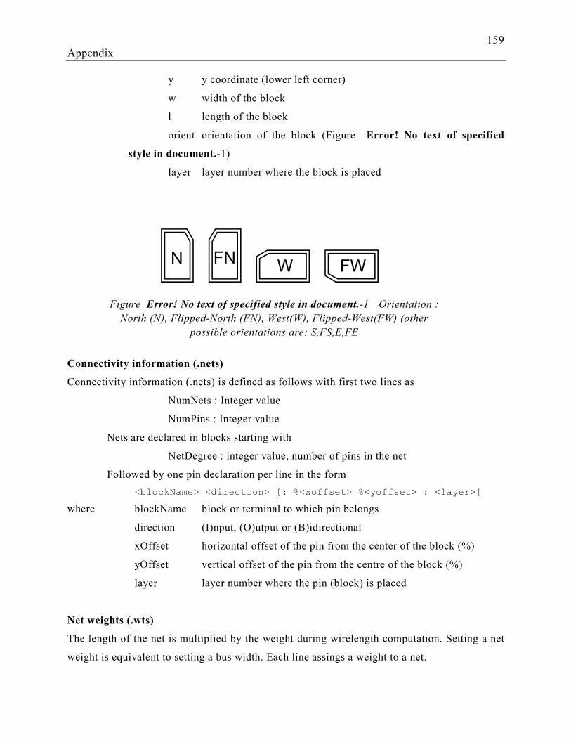
159
Appendix
y y coordinate (lower left corner)
w width of the block
l length of the block
orient orientation of the block (Figure Error! No text of specified
style in document.-1)
layer layer number where the block is placed
Connectivity information (.nets)
Connectivity information (.nets) is defined as follows with first two lines as
NumNets : Integer value
NumPins : Integer value
Nets are declared in blocks starting with
NetDegree : integer value, number of pins in the net
Followed by one pin declaration per line in the form
<blockName> <direction> [: %<xoffset> %<yoffset> : <layer>]
where blockName block or terminal to which pin belongs
direction (I)nput, (O)utput or (B)idirectional
xOffset horizontal offset of the pin from the center of the block (%)
yOffset vertical offset of the pin from the centre of the block (%)
layer layer number where the pin (block) is placed
Net weights (.wts)
The length of the net is multiplied by the weight during wirelength computation. Setting a net
weight is equivalent to setting a bus width. Each line assings a weight to a net.
N FNW FW
Figure Error! No text of specified style in document.-1 Orientation :
North (N), Flipped-North (FN), West(W), Flipped-West(FW) (other
possible orientations are: S,FS,E,FE
160
Appendix
<netName> <value>
Power information (.power)
This is defined in first two lines of the file with input values and a scaling factor.
PowerType : (P) for input in W, (D) for power density in W/m2
Scale : multiplication factor
Then the following line assigns a value to each block. Terminals are not considered.
<blockName> <value>
Stack technology (.stack)
Each line links a device technology to an integration technology. Technologies are referenced
by their tags.
<deviceTechnologyTag> <integrationTechnologyTag>
HotSpot I/O
Simulator configuration (.config)
For the purpose of optimization the only necessary parameters are:
Parameter Feature
-ambient ambient temperature in K
-r convec convection resistance
-t sink heatsink thickness
-k sink heatsink thermal conductivity
-t spreader spreader thickness
-k spreader spreader thermal conductivity
Layer Constraint File (.lcf)
Layers are described in block of 7 lines. The parameters are entered in the following order, one
per line.
Parameter Value
layer number layer index (sequential, starting at 0)

161
Appendix
lateral heat flow (Y)es, (N)o
power dissipation (Y)es, (N)o, yes for active layers
specific heat capacity not used (transient analysis)
thermal resistivity in m.K/W
thickness in m
162
Publications
PUBLICATIONS (JOURNAL, CONFERENCES, COLLOQUE, WORKSHOPS)
• Viswanathan.V, Frantz.F, Feng.Z, Navarro.D, O’Connor.I, 3D-IC: Fast imager thermal
modeling, Elsevier Journal of System Architecture (JSA). (Under review)
• Feng.Z, Viswanathan.V, Navarro.D, O’Connor.I, Image sensor matrix high speed
simulation, ICECS 2012 , (Accepted – To be presented on Nov 14-16,2012, Venice, Italy)
• Viswanathan.V, Frantz.F,Feng.Z,Navarro.D,O’Connor.I, Imager temperature
modeling,WASC Smart Camera, Clermont Ferrand, France, April 5-6,2012
• Viswanathan.V,Labrak.L, Frantz.F,Navarro.D,O’Connor.I, “Model based design of
Imager using abstraction segregated parameter dependency graphs”, NEWCAS 2011,
Bordeaux, France, June 26-29,2011.
• Navarro.D, Feng.Z, Viswanathan.V,Carrel.L,O’Connor.I, “Imager tool box for CMOS
image sensors in Cadence ADE”, Demset 2011, Orlando, Florida, USA, November 29th –
December 2nd, 2011
• Viswanathan.V, Labrak.L, Frantz.F, Navarro.D, O’Connor.I,” Model based design of
Imager pixel matrix” , GDR SoC SiP colloque 2011, Lyon, France.
• Viswanathan.V, Labrak.L, Frantz.F, Navarro.D, O’Connor.I, “Model based design of
Imager pixel matrix” , GDR Green SoC SiP colloque 2011, Montpellier, France. (Poster)
• Viswanathan.V, Navarro.D,Labrak.L, O’Connor.I, “High level modeling of Imager IC”,
GDR SoC SiP 2010, Paris, France.
• Viswanathan.V, Navarro.D,Labrak.L, O’Connor.I, “High level modeling of Imager IC”,
D43D workshop 2010, Lausanne, Switzerland. (Poster)
• Frantz.F,Labrak.L,Viswanathan.V, O’Connor.I, “Heterogeneous 3D design methods and
tools”, FETCH 2010, Chamonix, France. (Poster)