mips pipeline - cornell university
TRANSCRIPT
Hakim WeatherspoonCS 3410, Spring 2012Computer ScienceCornell University
MIPS Pipeline
See P&H Chapter 4.6
2
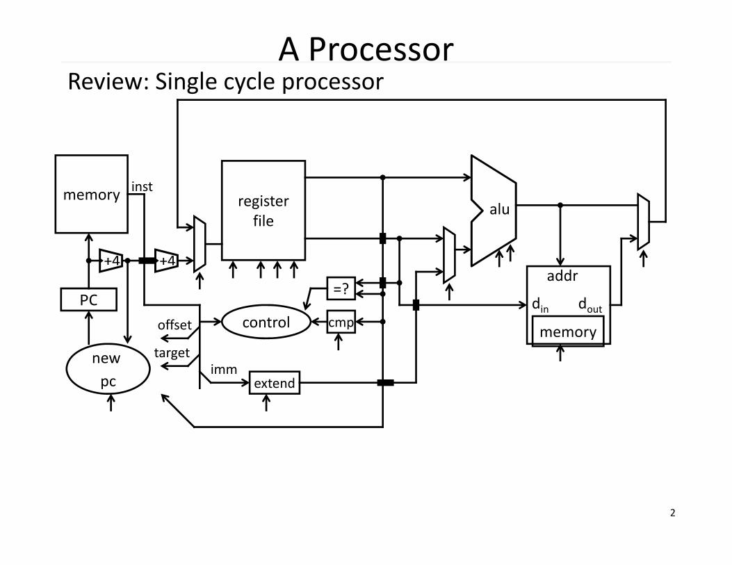
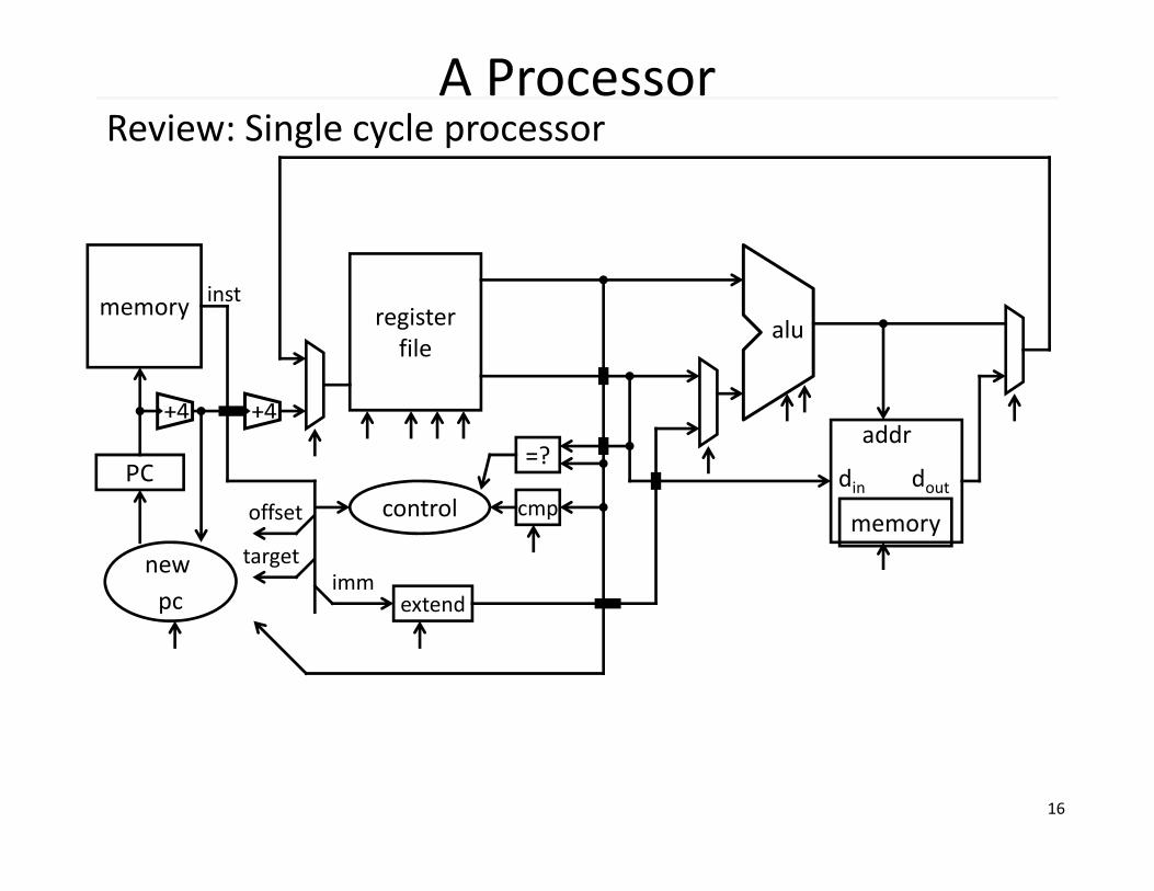
A Processor
alu
PC
imm
memory
memory
din dout
addr
target
offset cmpcontrol
=?
new pc
registerfile
inst
extend
+4 +4
Review: Single cycle processor
3
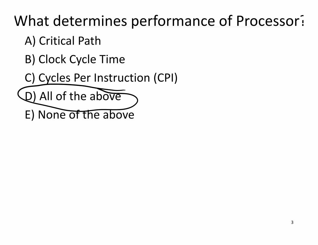
What determines performance of Processor?A) Critical PathB) Clock Cycle TimeC) Cycles Per Instruction (CPI)D) All of the aboveE) None of the above
4
Review: Single Cycle ProcessorAdvantages• Single Cycle per instruction make logic and clock simple
Disadvantages• Since instructions take different time to finish, memory and functional unit are not efficiently utilized.
• Cycle time is the longest delay.– Load instruction
• Best possible CPI is 1– However, lower MIPS and longer clock period (lower clock frequency); hence, lower performance.
5
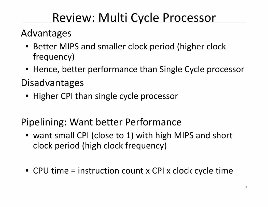
Review: Multi Cycle ProcessorAdvantages• Better MIPS and smaller clock period (higher clock frequency)
• Hence, better performance than Single Cycle processor Disadvantages• Higher CPI than single cycle processor
Pipelining: Want better Performance• want small CPI (close to 1) with high MIPS and short clock period (high clock frequency)
• CPU time = instruction count x CPI x clock cycle time
6
Single Cycle vs Pipelined Processor
See: P&H Chapter 4.5

7
The KidsAlice
Bob
They don’t always get along…

8
The Bicycle

9
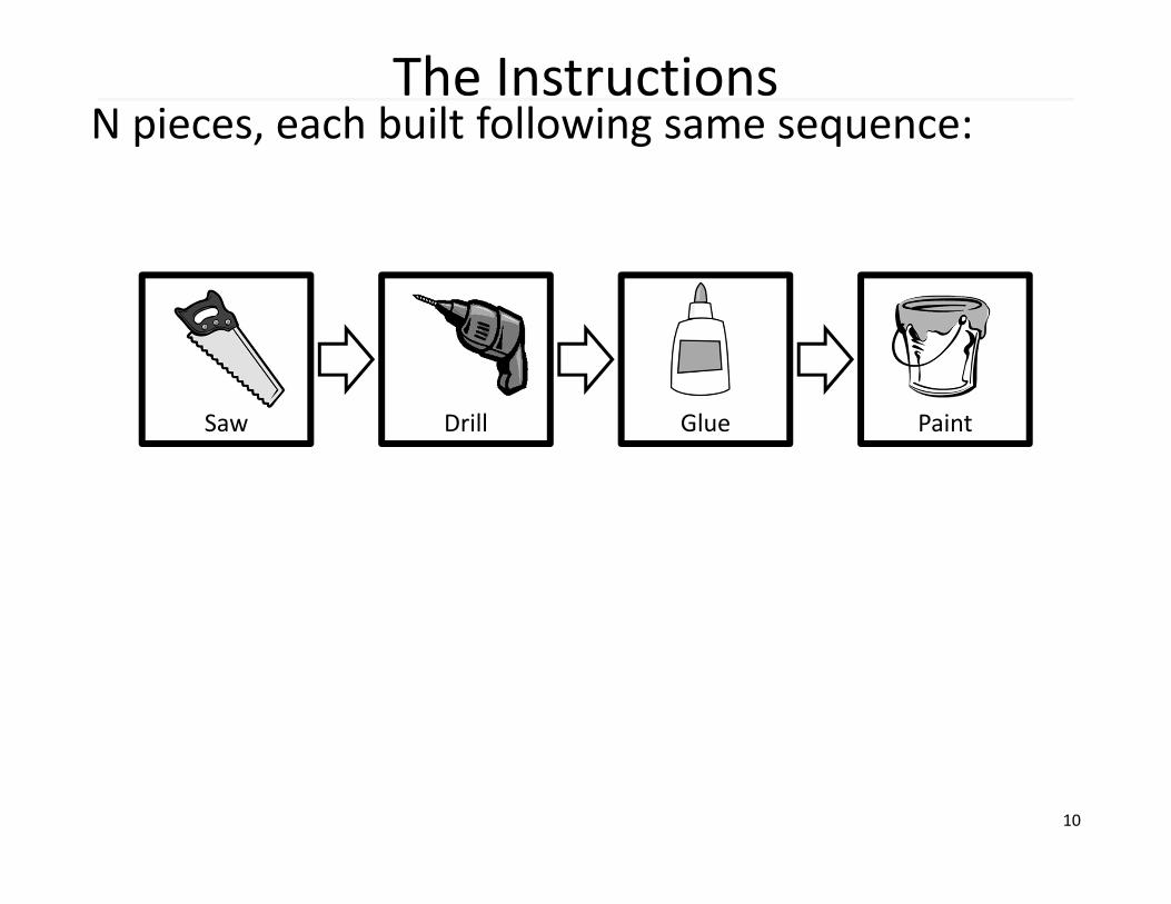
The Materials
Saw Drill
Glue Paint
10
The InstructionsN pieces, each built following same sequence:
Saw Drill Glue Paint
11
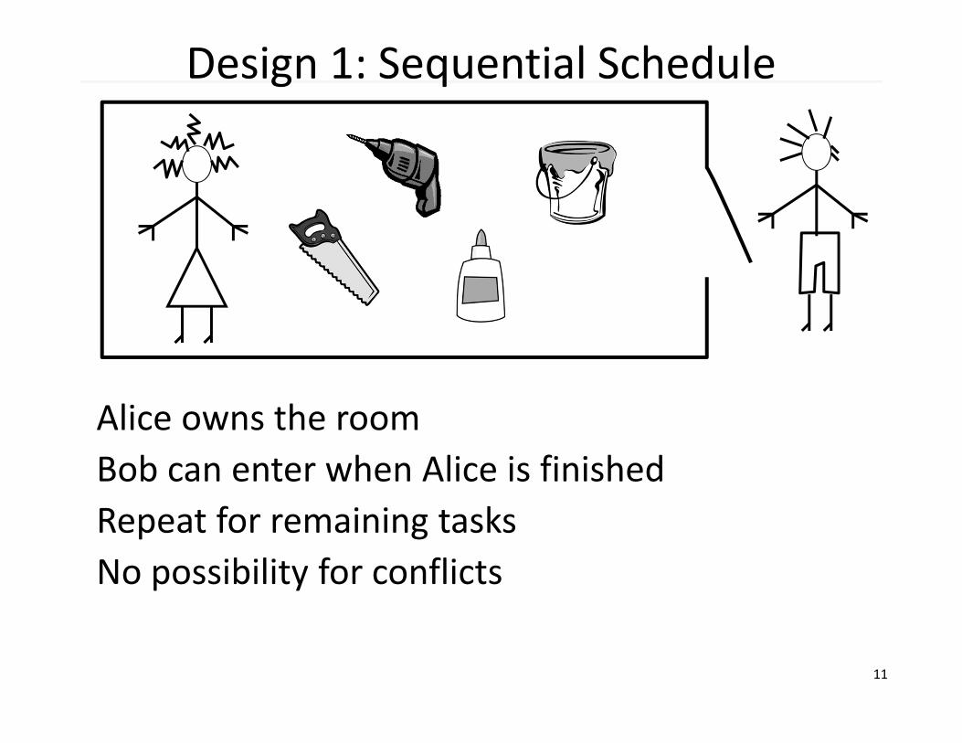
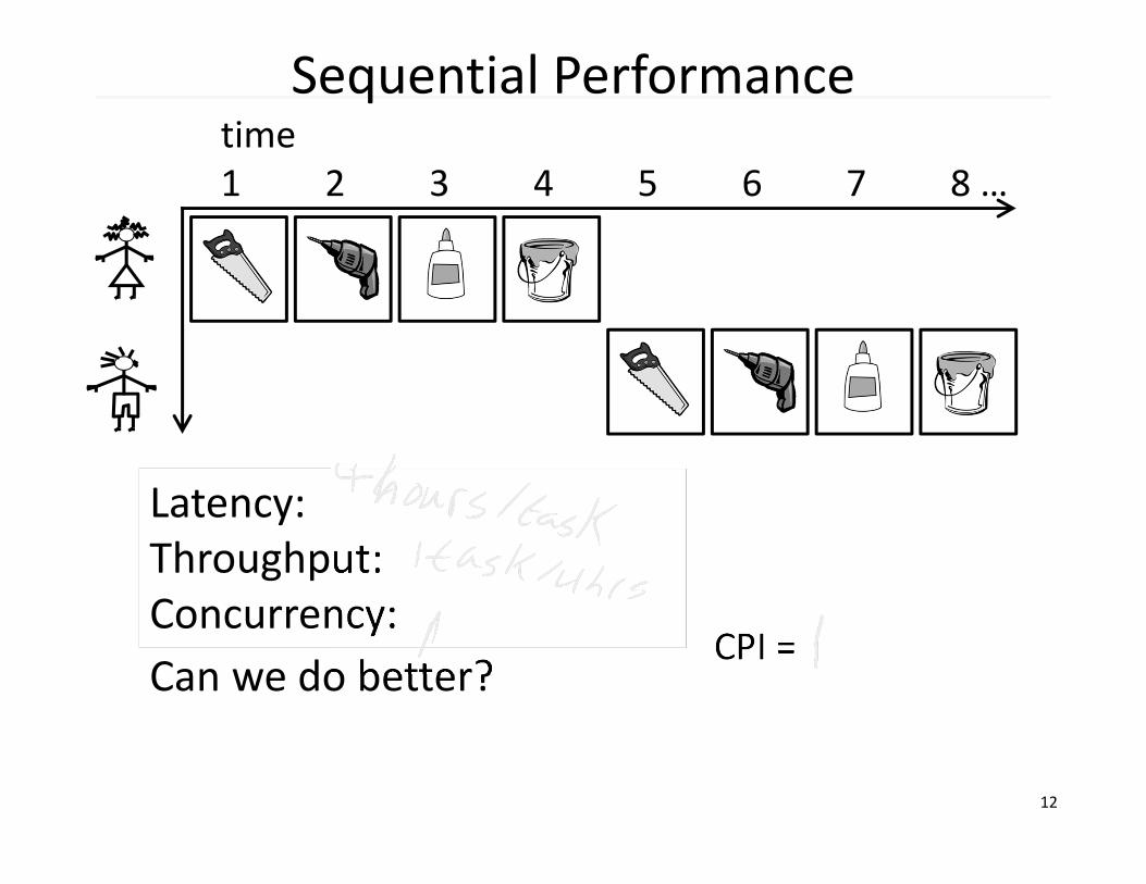
Design 1: Sequential Schedule
Alice owns the roomBob can enter when Alice is finishedRepeat for remaining tasksNo possibility for conflicts
12
Elapsed Time for Alice: 4Elapsed Time for Bob: 4Total elapsed time: 4*NCan we do better?
Sequential Performancetime1 2 3 4 5 6 7 8 …
Latency:Throughput:Concurrency:
CPI =
13
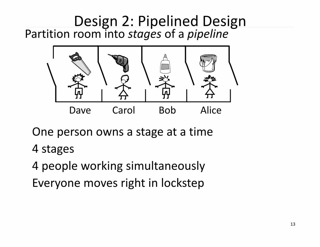
Design 2: Pipelined DesignPartition room into stages of a pipeline
One person owns a stage at a time4 stages4 people working simultaneouslyEveryone moves right in lockstep
AliceBobCarolDave
14
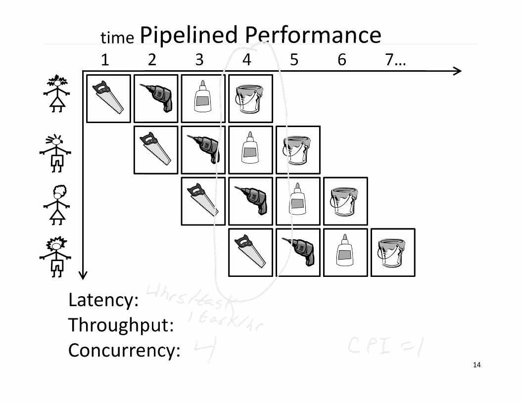
Pipelined Performancetime1 2 3 4 5 6 7…
Latency:Throughput:Concurrency:
15
LessonsPrinciple:Throughput increased by parallel execution
Pipelining:• Identify pipeline stages• Isolate stages from each other• Resolve pipeline hazards (Thursday)
16
A Processor
alu
PC
imm
memory
memory
din dout
addr
target
offset cmpcontrol
=?
new pc
registerfile
inst
extend
+4 +4
Review: Single cycle processor
17
Write‐BackMemory
InstructionFetch Execute
InstructionDecode
registerfile
control
A Processor
alu
imm
memory
din dout
addr
inst
PC
memory
computejump/branch
targets
new pc
+4
extend
18
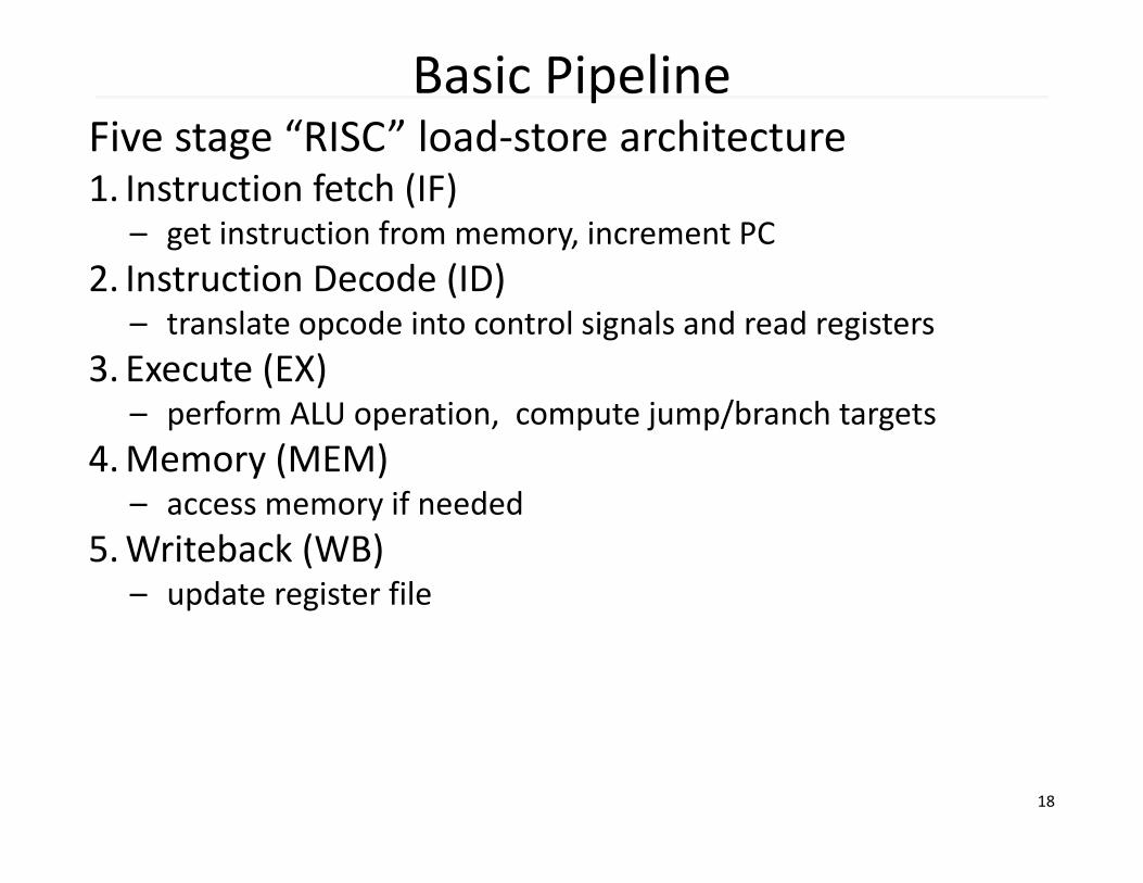
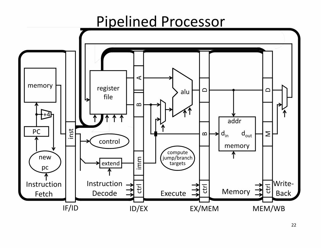
Basic PipelineFive stage “RISC” load‐store architecture1. Instruction fetch (IF)
– get instruction from memory, increment PC2. Instruction Decode (ID)
– translate opcode into control signals and read registers3. Execute (EX)
– perform ALU operation, compute jump/branch targets4.Memory (MEM)
– access memory if needed5.Writeback (WB)
– update register file
19
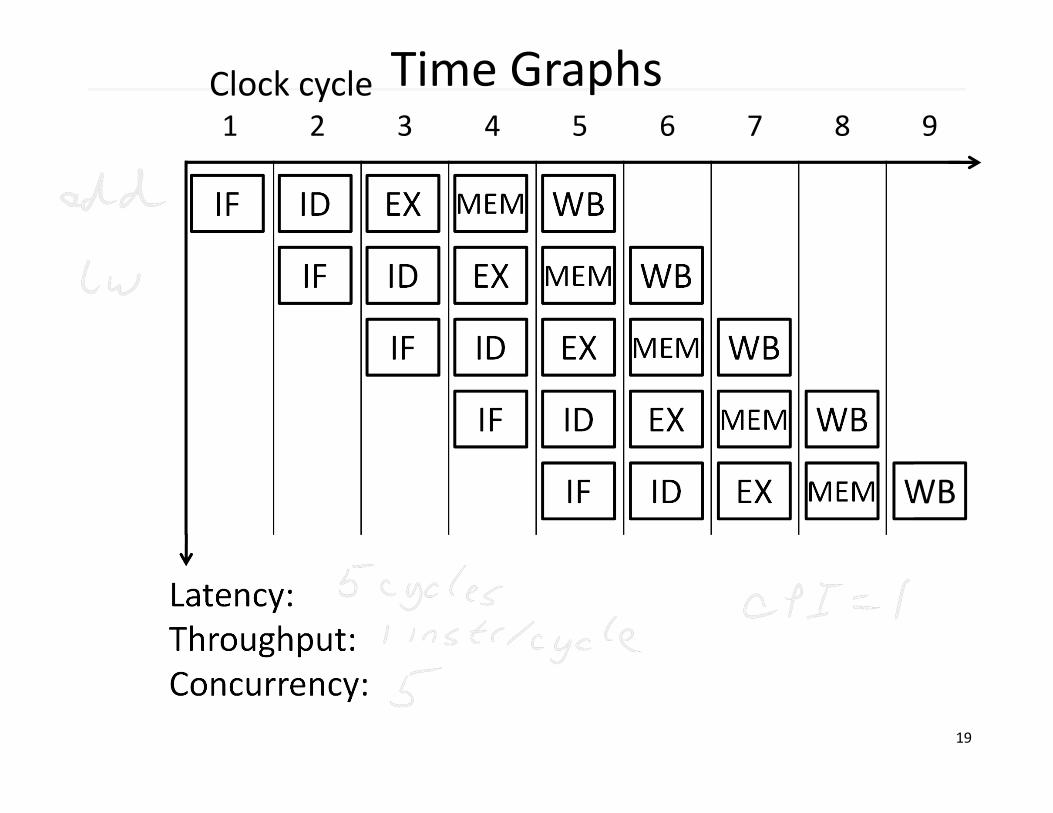
Time Graphs1 2 3 4 5 6 7 8 9Clock cycle
Latency:Throughput:Concurrency:
IF ID EX MEM WB
IF ID EX MEM WB
IF ID EX MEM WB
IF ID EX MEM WB
IF ID EX MEM WB
20
Principles of Pipelined ImplementationBreak instructions across multiple clock cycles (five, in this case)
Design a separate stage for the execution performed during each clock cycle
Add pipeline registers (flip‐flops) to isolate signals between different stages
21
Pipelined Processor
See: P&H Chapter 4.6
22
Write‐BackMemory
InstructionFetch Execute
InstructionDecode
extend
registerfile
control
Pipelined Processor
alu
memory
din dout
addrPC
memory
newpc
inst
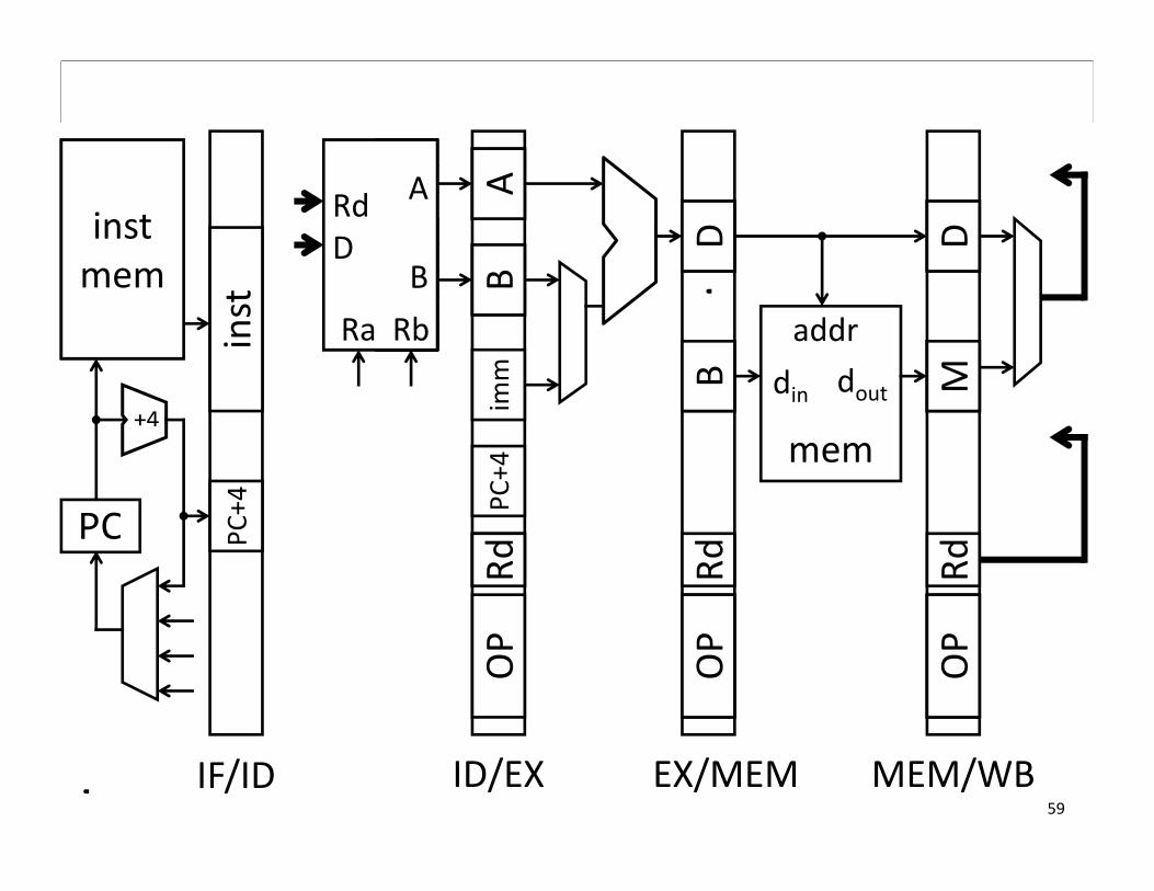
IF/ID ID/EX EX/MEM MEM/WB
imm
BA
ctrl
ctrl
ctrl
BD D
M
computejump/branch
targets
+4
23
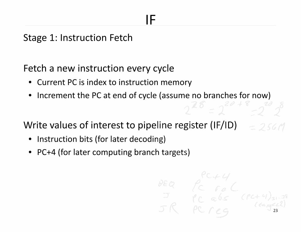
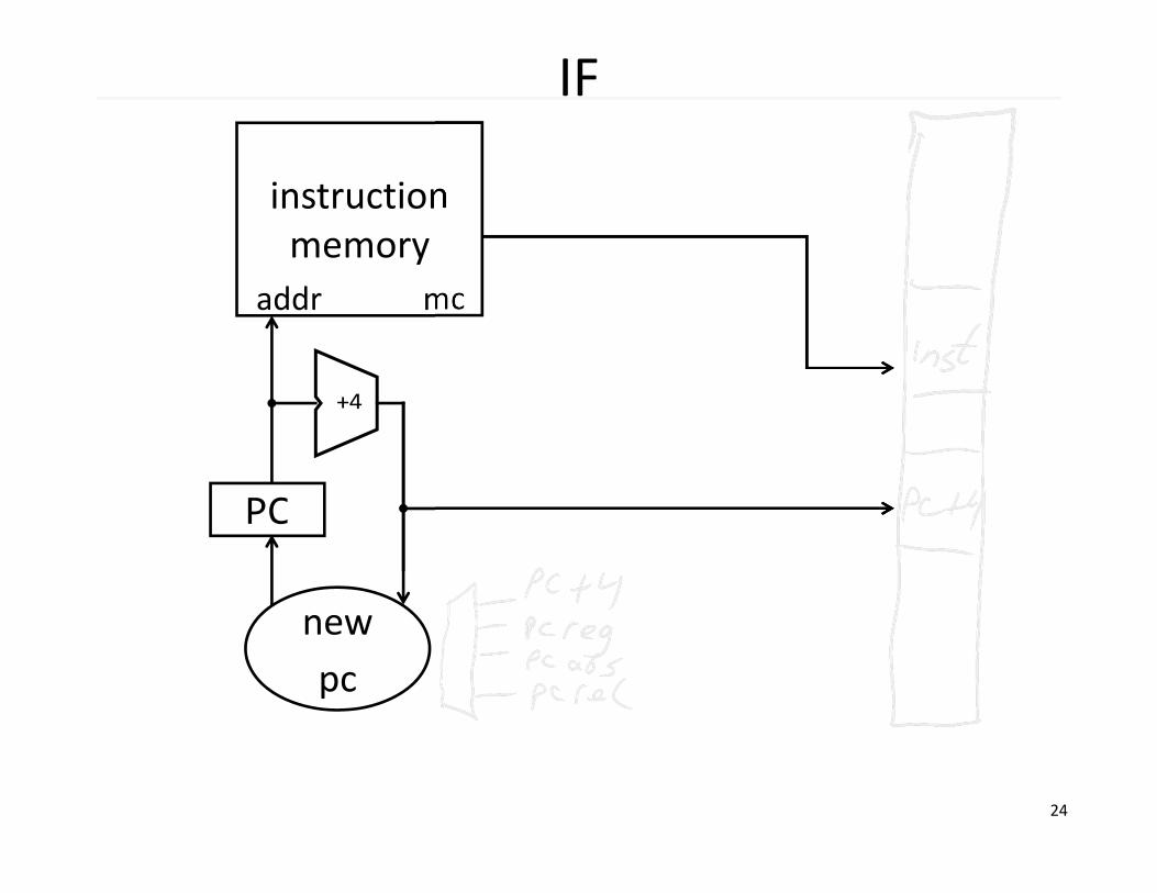
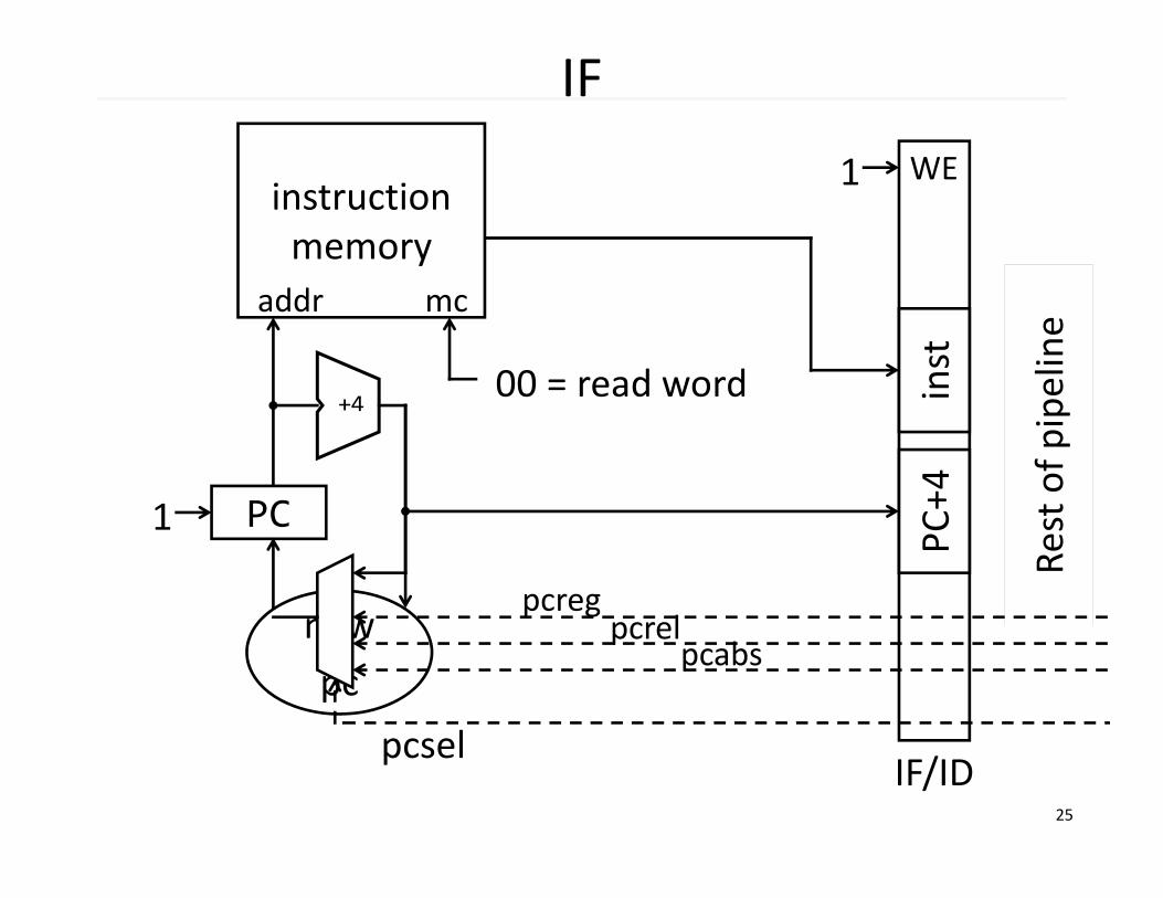
IFStage 1: Instruction Fetch
Fetch a new instruction every cycle• Current PC is index to instruction memory• Increment the PC at end of cycle (assume no branches for now)
Write values of interest to pipeline register (IF/ID)• Instruction bits (for later decoding)• PC+4 (for later computing branch targets)
24
IF
PC
instructionmemory
newpc
addr mc
+4
25
IF
PC
instructionmemory
newpc
inst
addr mc
00 = read word
1
IF/ID
WE1
Rest of p
ipeline
+4
PC+4
pcsel
pcregpcrel
pcabs
26
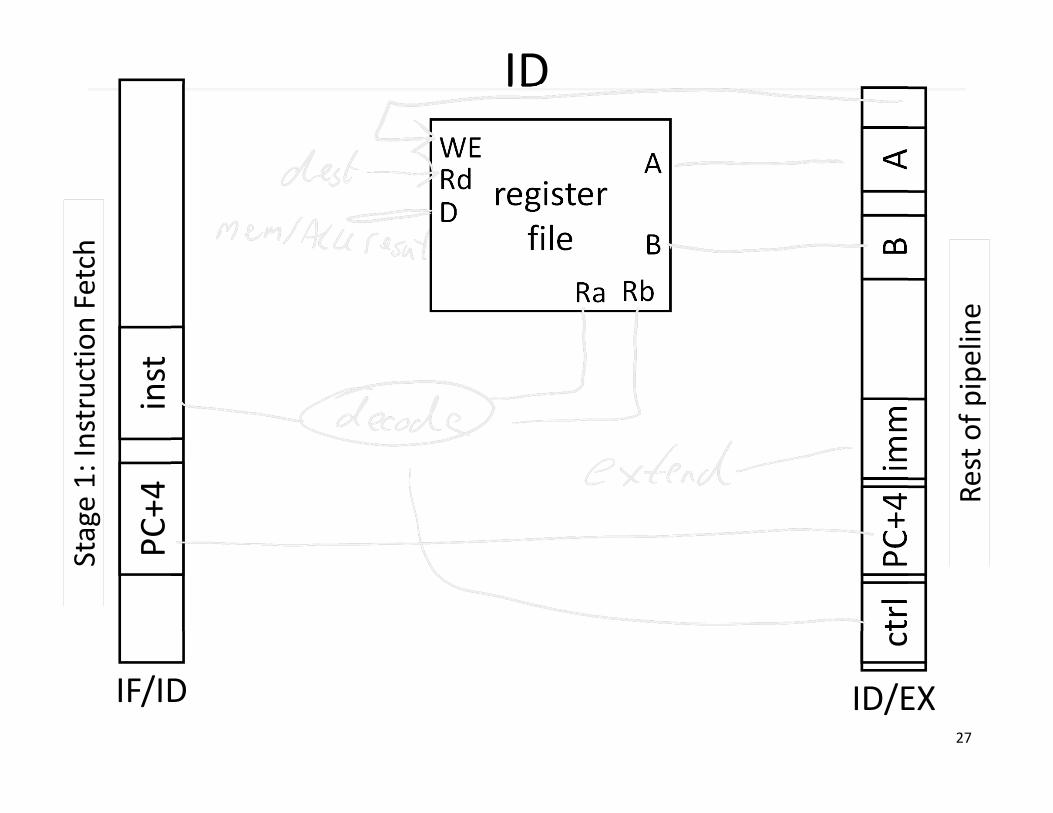
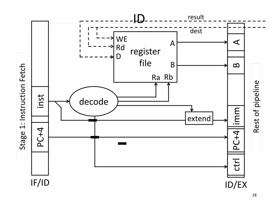
IDStage 2: Instruction Decode
On every cycle:• Read IF/ID pipeline register to get instruction bits• Decode instruction, generate control signals• Read from register file
Write values of interest to pipeline register (ID/EX)• Control information, Rd index, immediates, offsets, …• Contents of Ra, Rb• PC+4 (for computing branch targets later)
27
ID
ctrl
ID/EX
Rest of p
ipeline
PC+4
inst
IF/ID
PC+4
Stage 1: Instruction Fetch
registerfile
WERd
Ra Rb
DB
A
BA
imm
28
ID
ctrl
ID/EX
Rest of p
ipeline
PC+4
inst
IF/ID
PC+4
Stage 1: Instruction Fetch
registerfile
WERd
Ra Rb
DB
A
BA
extend imm
decode
result
dest
29
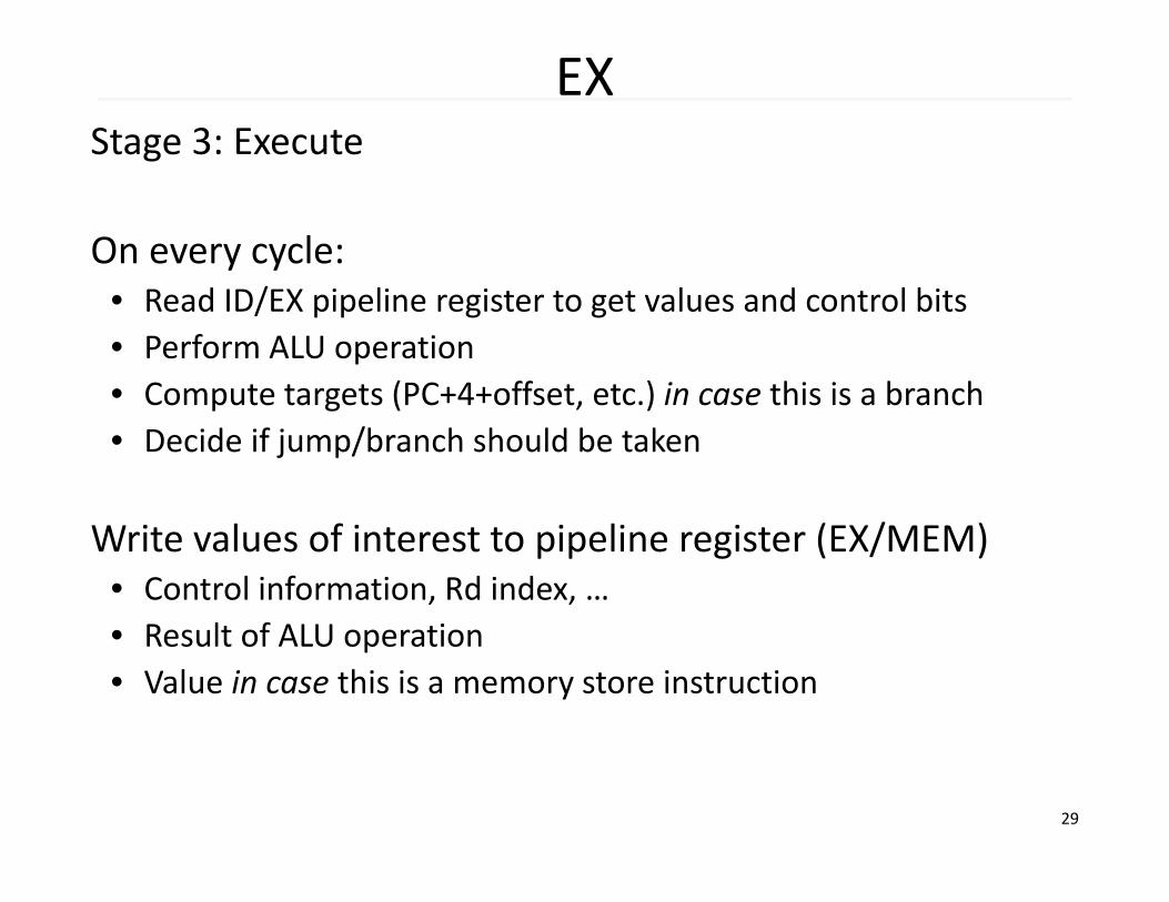
EXStage 3: Execute
On every cycle:• Read ID/EX pipeline register to get values and control bits• Perform ALU operation• Compute targets (PC+4+offset, etc.) in case this is a branch• Decide if jump/branch should be taken
Write values of interest to pipeline register (EX/MEM)• Control information, Rd index, …• Result of ALU operation• Value in case this is a memory store instruction
30
Stage 2: Instruction De
code
pcrel
pcabs
EX
ctrl
EX/MEM
Rest of p
ipeline
BD
ctrl
ID/EX
PC+4
BA
alu
j+
||
branch?
imm
pcselpcreg
target
31
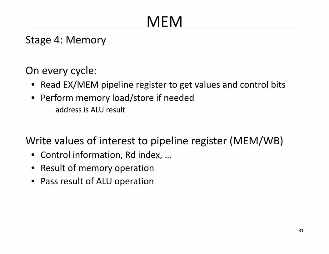
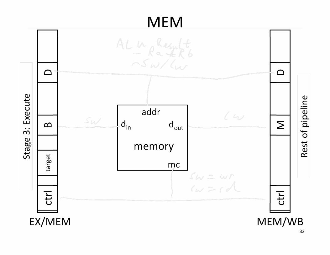
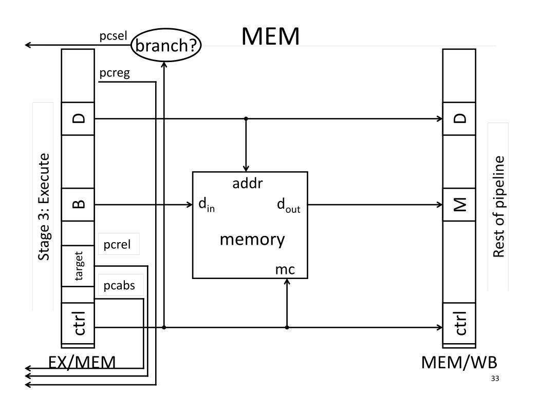
MEMStage 4: Memory
On every cycle:• Read EX/MEM pipeline register to get values and control bits• Perform memory load/store if needed
– address is ALU result
Write values of interest to pipeline register (MEM/WB)• Control information, Rd index, …• Result of memory operation• Pass result of ALU operation
32
MEM
ctrl
MEM/WB
Rest of p
ipeline
Stage 3: Execute
MD
ctrl
EX/MEM
BD
memory
din doutaddr
mctarget
33
MEM
ctrl
MEM/WB
Rest of p
ipeline
Stage 3: Execute
MD
ctrl
EX/MEM
BD
memory
din doutaddr
mctarget
branch?pcsel
pcrel
pcabs
pcreg
34
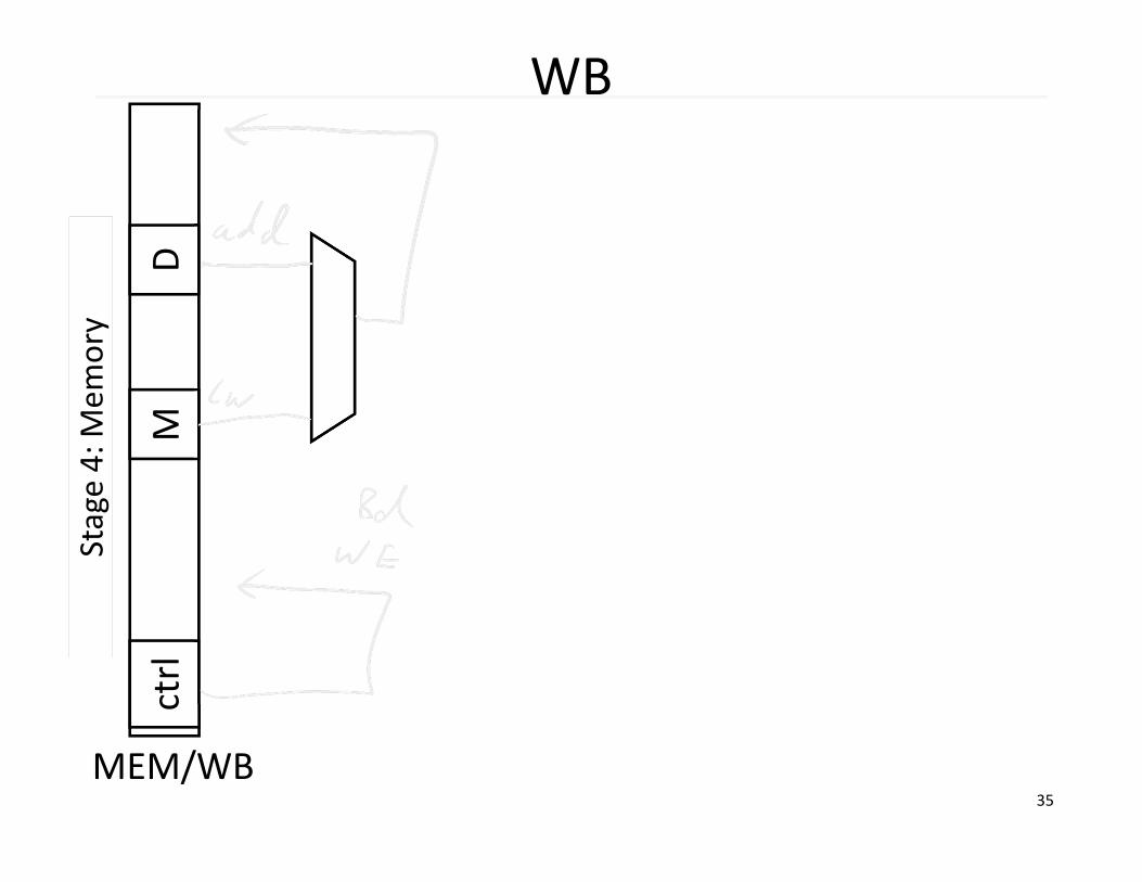
WBStage 5: Write‐back
On every cycle:• Read MEM/WB pipeline register to get values and control bits• Select value and write to register file
35
WBStage 4: M
emory
ctrl
MEM/WB
MD
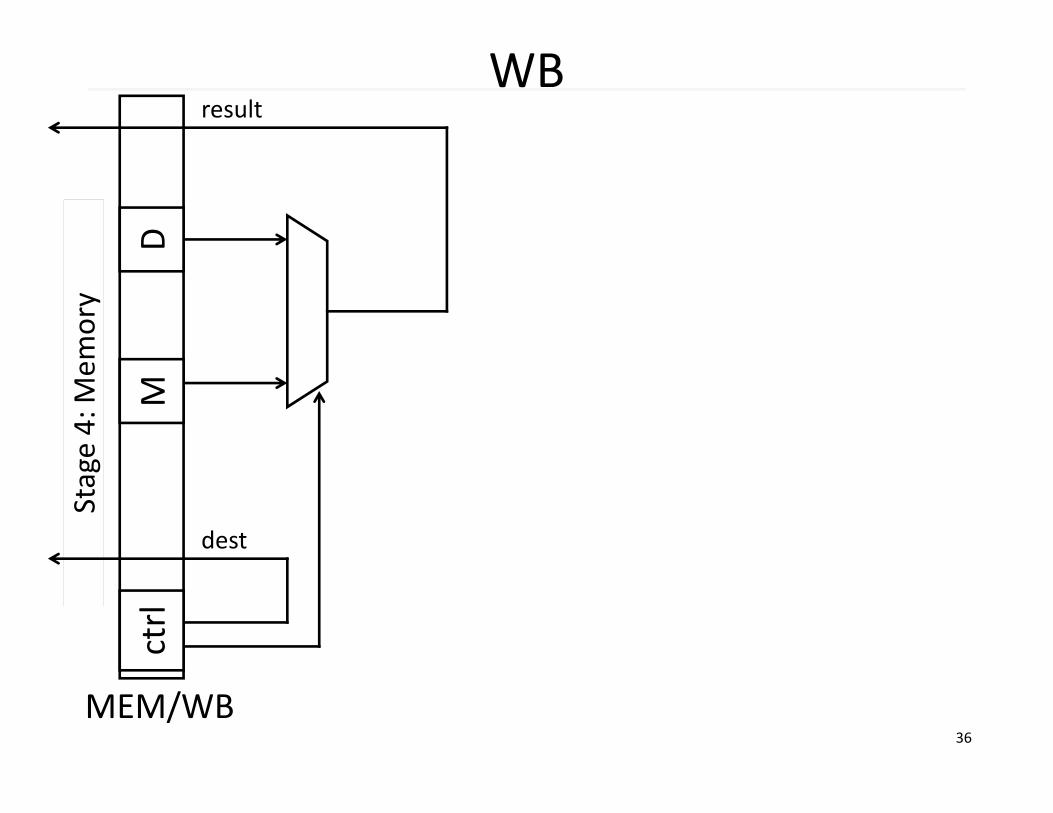
36
WBStage 4: M
emory
ctrl
MEM/WB
MD
result
dest

37IF/ID
+4
ID/EX EX/MEM MEM/WB
mem
din dout
addrinst
PC+4
OP
BA
Rt
BD
MD
PC+4
imm
OP
Rd
OP
Rd
PC
instmem
Rd
Ra Rb
DB
A
Rd

38
AdministriviaHW2 due today
• Fill out Survey online. Receive credit/points on homework for survey:• https://cornell.qualtrics.com/SE/?SID=SV_5olFfZiXoWz6pKI• Survey is anonymous
Project1 (PA1) due week after prelim• Continue working diligently. Use design doc momentum
Save your work!• Save often. Verify file is non‐zero. Periodically save to Dropbox, email.• Beware of MacOSX 10.5 (leopard) and 10.6 (snow‐leopard)
Use your resources• Lab Section, Piazza.com, Office Hours, Homework Help Session,• Class notes, book, Sections, CSUGLab
39
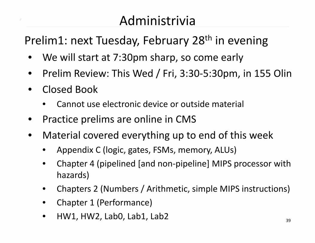
AdministriviaPrelim1: next Tuesday, February 28th in evening• We will start at 7:30pm sharp, so come early• Prelim Review: This Wed / Fri, 3:30‐5:30pm, in 155 Olin• Closed Book
• Cannot use electronic device or outside material
• Practice prelims are online in CMS• Material covered everything up to end of this week
• Appendix C (logic, gates, FSMs, memory, ALUs) • Chapter 4 (pipelined [and non‐pipeline] MIPS processor with
hazards)• Chapters 2 (Numbers / Arithmetic, simple MIPS instructions)• Chapter 1 (Performance)• HW1, HW2, Lab0, Lab1, Lab2

40
Administrivia
Check online syllabus/schedule • http://www.cs.cornell.edu/Courses/CS3410/2012sp/schedule.htmlSlides and Reading for lecturesOffice HoursHomework and Programming AssignmentsPrelims (in evenings):
• Tuesday, February 28th
• Thursday, March 29th
• Thursday, April 26th
Schedule is subject to change
41
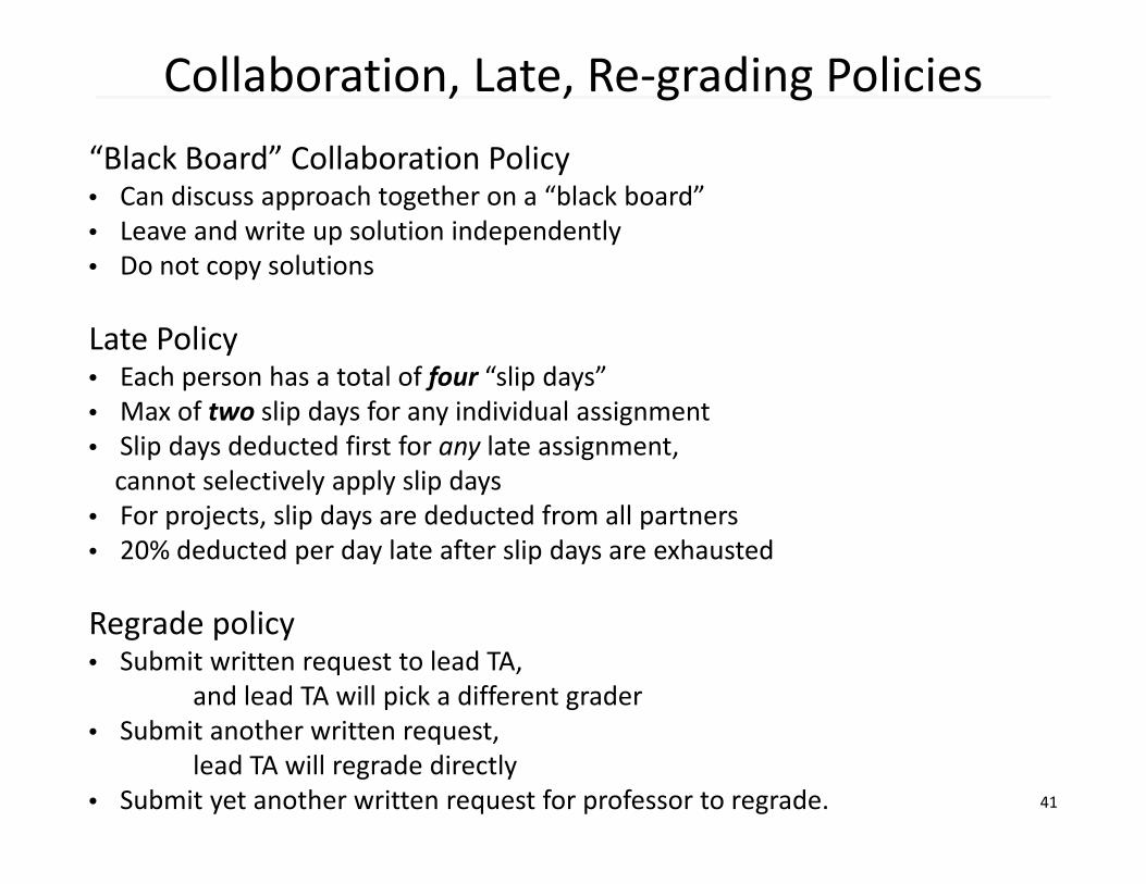
Collaboration, Late, Re‐grading Policies“Black Board” Collaboration Policy• Can discuss approach together on a “black board”• Leave and write up solution independently• Do not copy solutions
Late Policy• Each person has a total of four “slip days”• Max of two slip days for any individual assignment• Slip days deducted first for any late assignment, cannot selectively apply slip days
• For projects, slip days are deducted from all partners • 20% deducted per day late after slip days are exhausted
Regrade policy• Submit written request to lead TA,
and lead TA will pick a different grader • Submit another written request,
lead TA will regrade directly • Submit yet another written request for professor to regrade.
42
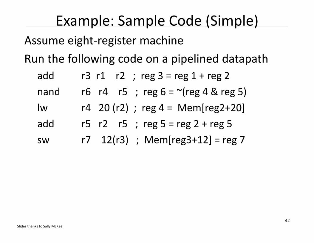
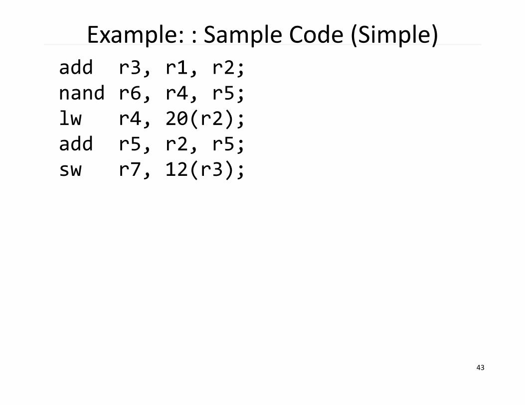
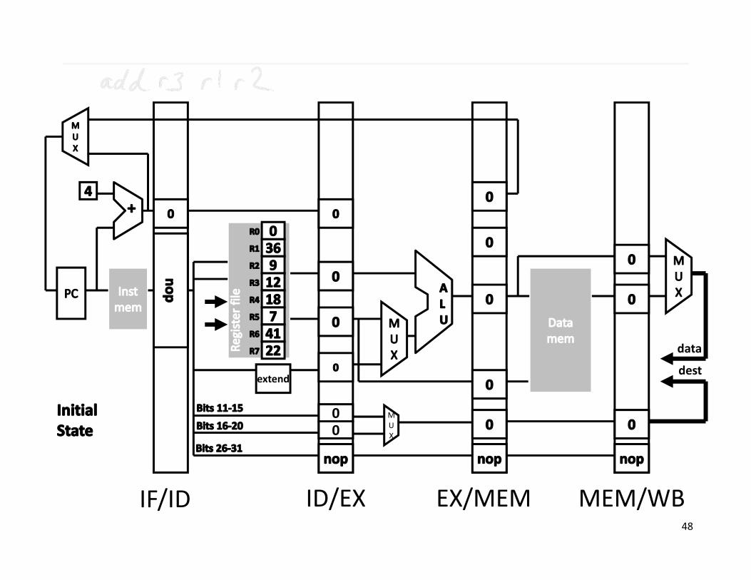
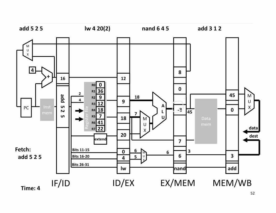
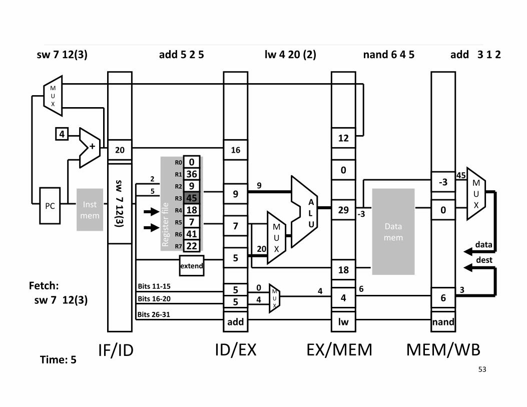
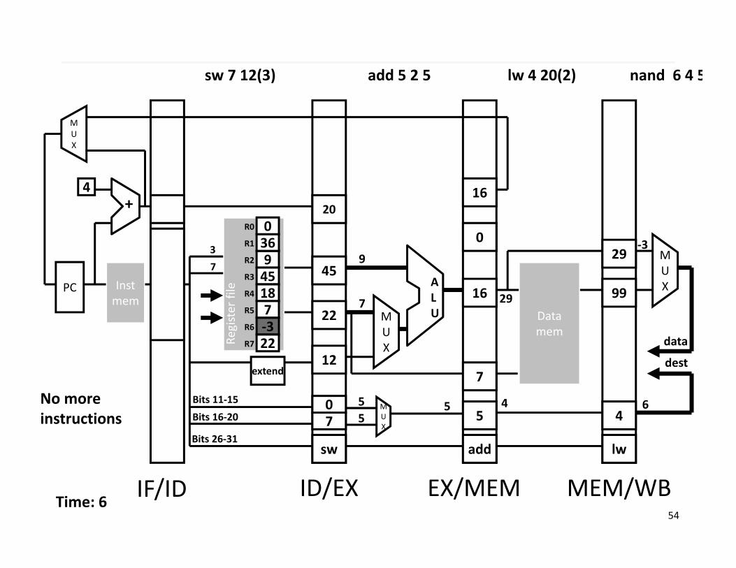
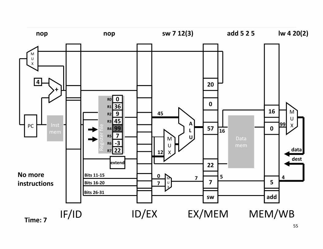
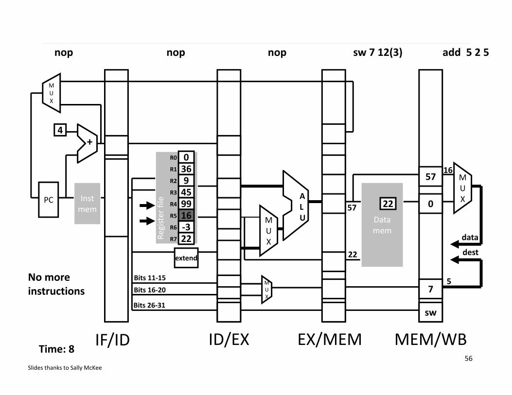
Example: Sample Code (Simple)Assume eight‐register machineRun the following code on a pipelined datapath
add r3 r1 r2 ; reg 3 = reg 1 + reg 2nand r6 r4 r5 ; reg 6 = ~(reg 4 & reg 5)lw r4 20 (r2) ; reg 4 = Mem[reg2+20]add r5 r2 r5 ; reg 5 = reg 2 + reg 5sw r7 12(r3) ; Mem[reg3+12] = reg 7
Slides thanks to Sally McKee
43
Example: : Sample Code (Simple)add r3, r1, r2; nand r6, r4, r5; lw r4, 20(r2); add r5, r2, r5; sw r7, 12(r3);
44
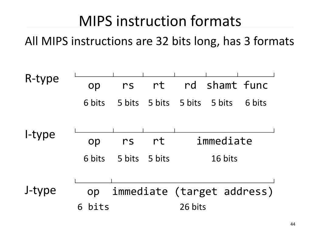
MIPS instruction formatsAll MIPS instructions are 32 bits long, has 3 formats
R‐type
I‐type
J‐type
op rs rt rd shamt func6 bits 5 bits 5 bits 5 bits 5 bits 6 bits
op rs rt immediate6 bits 5 bits 5 bits 16 bits
op immediate (target address)6 bits 26 bits
45
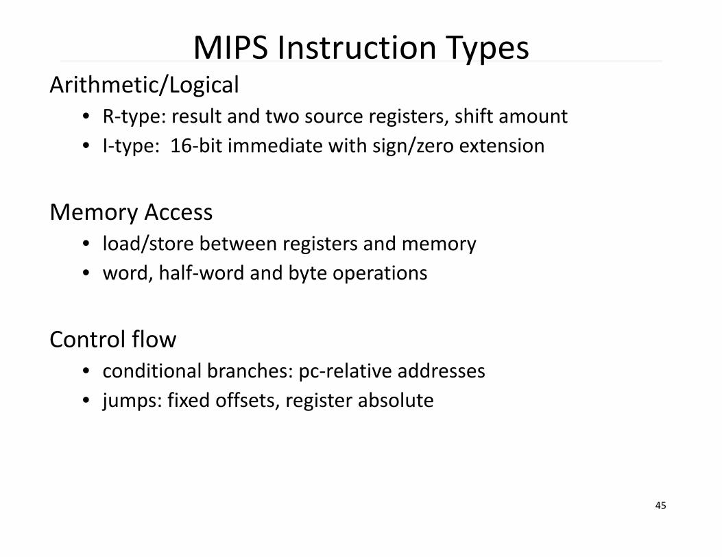
MIPS Instruction TypesArithmetic/Logical
• R‐type: result and two source registers, shift amount• I‐type: 16‐bit immediate with sign/zero extension
Memory Access• load/store between registers and memory• word, half‐word and byte operations
Control flow• conditional branches: pc‐relative addresses• jumps: fixed offsets, register absolute
46
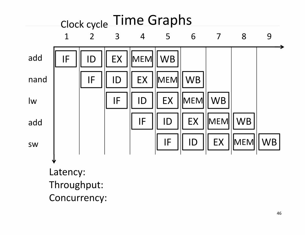
Time Graphs1 2 3 4 5 6 7 8 9
add
nand
lw
add
sw
Clock cycle
Latency:Throughput:Concurrency:
IF ID EX MEM WB
IF ID EX MEM WB
IF ID EX MEM WB
IF ID EX MEM WB
IF ID EX MEM WB
47
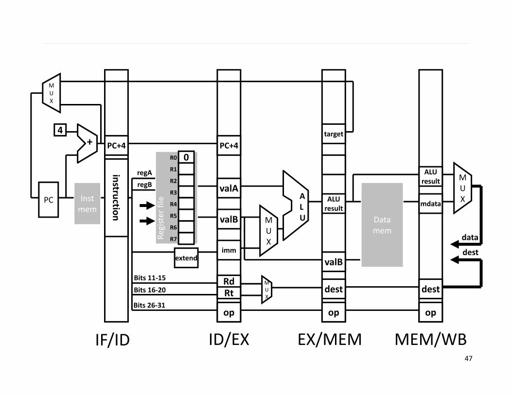
PC Instmem
Register file
MUXA
LU
MUX
4
Datamem
+
MUX
Bits 11‐15
Bits 16‐20
op
Rt
imm
valB
valA
PC+4PC+4target
ALUresult
op
dest
valB
op
dest
ALUresult
mdata
instruction
0
R2
R3
R4
R5
R1
R6
R0
R7
regAregB
Bits 26‐31
data
dest
IF/ID ID/EX EX/MEM MEM/WB
extend
MUX
Rd
48
data
dest
IF/ID ID/EX EX/MEM MEM/WB
extend
0MUX
0

49
PC Instmem
Register file
MUXA
LU
MUX
4
Datamem
+
MUX
Bits 11‐15
Bits 16‐20
nop
0
0
0
040
0
nop
0
0
nop
0
0
0
0
add 3 1 2
912187
36
41
0
22
R2
R3
R4
R5
R1
R6
R0
R7
Bits 26‐31
data
dest
Fetch:add 3 1 2
add 3 1 2
Time: 1 IF/ID ID/EX EX/MEM MEM/WB
extend
0MUX
0
50
PC Instmem
Register file
MUXA
LU
MUX
4
Datamem
+
MUX
Bits 11‐15
Bits 16‐20
add
3
9
36
480
0
nop
0
0
nop
0
0
0
0nand 6 4 5
912187
36
41
0
22
R2
R3
R4
R5
R1
R6
R0
R7
12
Bits 26‐31
data
dest
Fetch:nand 6 4 5
nand 6 4 5 add 3 1 2
Time: 2 IF/ID ID/EX EX/MEM MEM/WB
extend
2MUX
3

51
PC Instmem
Register file
MUXA
LU
MUX
4
Datamem
+
MUX
Bits 11‐15
Bits 16‐20
nand
6
7
18
8124
45
add
3
9
nop
0
0
0
0lw 4 20(2)
912187
36
41
0
22
R2
R3
R4
R5
R1
R6
R0
R7
45
Bits 26‐31
data
dest
Fetch:lw 4 20(2)
lw 4 20(2) nand 6 4 5 add 3 1 2
Time: 3
36
9
3
IF/ID ID/EX EX/MEM MEM/WB
extend
5MUX
6 32
52
PC Instmem
Register file
MUXA
LU
MUX
4
Datamem
+
MUX
Bits 11‐15
Bits 16‐20
lw
20
18
9
12168
‐3
nand
6
7
add
3
45
0
0add 5 2 5
912187
36
41
0
22
R2
R3
R4
R5
R1
R6
R0
R7
24
Bits 26‐31
data
dest
Fetch:add 5 2 5
add 5 2 5 lw 4 20(2) nand 6 4 5 add 3 1 2
Time: 4
18
7
6
45
3
IF/ID ID/EX EX/MEM MEM/WB
extend
4MUX
0 65
53
PC Instmem
Register file
MUXA
LU
MUX
4
Datamem
+
MUX
Bits 11‐15
Bits 16‐20
add
5
7
9
162012
29
lw
4
18
nand
6
‐3
0
0sw 7 12(3)
945187
36
41
0
22
R2
R3
R4
R5
R1
R6
R0
R7
25
Bits 26‐31
data
dest
Fetch:sw 7 12(3)
sw 7 12(3) add 5 2 5 lw 4 20 (2) nand 6 4 5 add 3 1 2
Time: 5
9
20
4
‐3
6
45
3
IF/ID ID/EX EX/MEM MEM/WB
extend
5MUX
5 04
54
PC Instmem
Register file
MUXA
LU
MUX
4
Datamem
+
MUX
Bits 11‐15
Bits 16‐20
sw
12
22
45
2016
16
add
5
7
lw
4
29
99
0945187
36
‐3
0
22
R2
R3
R4
R5
R1
R6
R0
R7
37
Bits 26‐31
data
dest
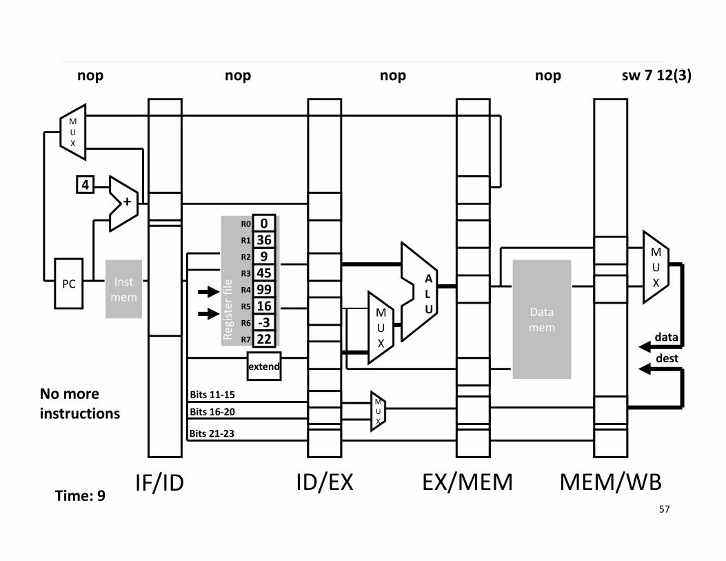
No moreinstructions
sw 7 12(3) add 5 2 5 lw 4 20(2) nand 6 4 5
Time: 6
9
7
5
29
4
‐3
6
IF/ID ID/EX EX/MEM MEM/WB
extend
7MUX
0 55
55
PC Instmem
Register file
MUXA
LU
MUX
4
Datamem
+
MUX
Bits 11‐15
Bits 16‐20
20
57
sw
7
22
add
5
16
0
0945997
36
‐3
0
22
R2
R3
R4
R5
R1
R6
R0
R7
Bits 26‐31
data
dest
No moreinstructions
nop nop sw 7 12(3) add 5 2 5 lw 4 20(2)
Time: 7
45
7
12
16
5
99
4
IF/ID ID/EX EX/MEM MEM/WB
extend
MUX
07
56
PC Instmem
Register file
MUXA
LU
MUX
4
Datamem
+
MUX
Bits 11‐15
Bits 16‐20
sw
7
57
0
9459916
36
‐3
0
22
R2
R3
R4
R5
R1
R6
R0
R7
Bits 26‐31
data
dest
No moreinstructions
nop nop nop sw 7 12(3) add 5 2 5
Time: 8
2257
22
16
5
Slides thanks to Sally McKee
IF/ID ID/EX EX/MEM MEM/WB
extend
MUX
57
PC Instmem
Register file
MUXA
LU
MUX
4
Datamem
+
MUX
Bits 11‐15
Bits 16‐20
9459916
36
‐3
0
22
R2
R3
R4
R5
R1
R6
R0
R7
Bits 21‐23
data
dest
No moreinstructions
nop nop nop nop sw 7 12(3)
Time: 9 IF/ID ID/EX EX/MEM MEM/WB
extend
MUX
58
Pipelining RecapPowerful technique for masking latencies• Logically, instructions execute one at a time• Physically, instructions execute in parallel
– Instruction level parallelism
Abstraction promotes decoupling• Interface (ISA) vs. implementation (Pipeline)
59
0:add1:nand2:lw3:add4:sw
r0r1r2r3r4r5r6r7
0369121874122
IF/ID
+4
ID/EX EX/MEM MEM/WB
mem
din dout
addrinst
PC+4
OP
BA
Rd
BD
MD
PC+4
imm
OP
Rd
OP
Rd
PC
instmem
77
add r3, r1, r2nand r6, r4, r5 add r3, r1, r2lw r4, 20(r2) nand r6, r4, r5 add r3, r1, r2add r5, r2, r5 lw r4, 20(r2) nand r6, r4, r5 add r3, r1, r2sw r7, 12(r3) add r5, r2, r5 lw r4, 20(r2) nand r6, r4, r5 add r3, r1, r2sw r7, 12(r3) add r5, r2, r5 lw r4, 20(r2) nand r6, r4, r5sw r7, 12(r3) add r5, r2, r5 lw r4, 20(r2)sw r7, 12(r3) add r5, r2, r5 sw r7, 12(r3)
Rd
Ra Rb
DB
A