mil-hdbk-978b - nasa parts application handbook volume 3 … · nasa parts application handbook...
TRANSCRIPT

MIL-HDBK-978-B (NASA) 1 MARCH 1988
SUPERSEDING MIL-HDBK-978-A (NASA)
15 MARCH 1984
MILITARY HANDBOOK
NASA PARTS APPLICATION HANDBOOK
(VOLUME 3 OF 5) MICROCIRCUITS
AMSC N/A FSC59GP DISTRIBUTION STATEMENT A. Approved for public release; distribution is unlimited


MIL-HDBK-978 B (NASA)
MIL-HDBK-978B (NASA)
NATIONAL AERONAUTICS AND SPACE ADMINISTRATION
WASHINGTON, D.C. 20546
NASA Parts Application Handbook
1. This handbook is approved for use by all elements of the National Aeronautics and Space Administration and is available for use by all departments and agencies of the Department of Defense.
2. Beneficial comments (recommendations, additions, deletions) and any pertinent data which may be of use in improving this document should be addressed to: Manager, NASA Parts Project Office, Goddard Space Flight Center, Greenbelt, Maryland 20771,
i

MIL-HDBK-978 B (NASA)
ii

MIL-HDBK-978-B (NASA)
FOREWORD
This handbook provides a technological baseline for parts used throughout NASA programs. The information included will improve the utilization of the NASA Standard Electrical, Electronic, and Electromechanical (EEE) Parts List (MIL-STD-975) and provide technical information to improve the selection of parts and their application, and failure analysis on all NASA projects. This handbook consists of five volumes and includes information on all parts presently included in MIL-STD-975.
This handbook (Revision B) succeeds the initial release. Revision A was not released. The con-tent in Revision B has been extensively changed from that in the initial release.
iii

MIL-HDBK-978-B (NASA)

MIL-HDBK-978-B (NASA)
CONTENTS
GENERAL CONTENTS
VOLUMES 1 through 5
VOLUME 1
Section 1. Introduction 2. Capacitors 3. Resistors and Thermistors
VOLUME 2
4. Diodes 5. Transistors 6. Microwave Devices
VOLUME 3
7. Microcircuits
VOLUME 4
8. Crystals 9. Filters
10/ Transformers and Inductors 11. Delay Lines 12. Motors
VOLUME 5
13. Connectors, Power 14. Connectors, Radio Frequency 15. Protective Devices 16. Switches 17. Relays 18. Wire and Cable
v

C O N T E N T S
MIL-HDBK-978-B (NASA)
THIS PAGE INTENTIONALLY LEFT BLANK
vi

MIL-HDBK-978-B (NASA)
CONTENTS
VOLUME CONTENTS
VOLUME 3 Paqe
Paragraph 7. MICROCIRCUITS - - - - 7-1 7.1 General - - - - - - - 7-1 7.1.1 Introduction- - - - - - - - - - - - - - - - - - - - 7-1 7.1.2 Definitions, abbreviations, conversion factors- - - 7-2 7.1.3 NASA standard parts - 7-26 7.1.4 General device character! sties- - - - - - - - - - - 7-27 7.1.5 General parameter information - - - - - - - - - - - 7-31 7.1.6 General guides and charts - - - - - - - - - - - - - 7-33 7.1.7 General reliability considerations- - - - - - - - - 7-37
7.2 Low-power Schottky transistor-t ransi stor logic- - - 7-51 7.2.1 Introduction- - - - - - - - - - - - - - - 7-51 7.2.2 Usual applications- - - - - - - - 7-51
7.2.3 Physical construction - - - - - - - - - - - - - - - 7-56 7.2.4 Military designation- - - - - - - - - - - - - - - - 7-58 7.2.5 Electrical characteristics- - - - - - - - - - - - - 7-58 7.2.6 Environmental considerations- - - - - - - - - - - - 7-60 7.2.7 Reliability considerations- - - - - - - - - - - - - 7-60
7.3 Advanced low-power Schottky transistor-transistor l o g i c - - - - - - - - - - - - - - - - - - - - - - - 7-61
7.3.1 Introduction- - - - - - - - - - - - - - - - — - - 7-61 7.3.2 Usual applications- - - - - - - - - - - - - - - - - 7-61 7.3.3 Physical construction - - - - - - - - - - - - - - - 7-63 7.3.4 Military designation- - - - - - - - - - - - - - - - 7-65 7.3.5 Electrical characteristies- - - - - - - - - - - - - 7-66 7.3.6 Environmental considerations- - - - - - - - - - - - 7-67 7.3.7 Reliability considerations- - - - - - - - - - - - - 7-67
7.4 Advanced Schottky transistor-transistor logic - - - 7-68 7.4.1 Introduction- - - - - - - - - - - - - - - - - - — 7-68 7.4.2 Usual applications- - - - - - - - - - - - - - - - - 7-68 7.4.3 Physical construction - - - - - - - - - - - - - - - 7-70 7.4.4 Military d e s i g n a t i o n— - - - - - - - - - 7-70 7.4.5 Electrical characteristics- - - - - 7-70 7.4.6 Environmental considerations- - - - - - - - - - - - 7-72 7.4.7 Reliability considerations- - - - - - - - - - - - - 7-72
7.5 CMOS 4000B series - 7-73 7.5.1 Introduction- - - - - - - - - - - - - - - - - - - - 7-73 7.5.2 Usual a p p l i c a t i o n s— - - - - - - - - - - - - - - - 7-73 7.5.3 Physical construction - - - - - - - - - - - - - - - 7-75
vi i

MIL-HDBK-978-B (NASA)
CONTENTS
VOLUME CONTENTS
VOLUME 3
Pa^e
Paragraph 7.5.4 Military designation- - - — - - - - - - - - - - - 7-76 7.5.5 Electrical characteristics- - - - - - - - - - - - - 7-76 7.5.6 Environmental considerations- - - - - - - - - - — 7-77 7.5.7 Reliability considerations- - - - - - - - - - - - - 7-77
7.6 High-speed CMOS series - - - - - 7-78 7.6.1 Introduction- - - - - - - - - - - - - - - - - - - - 7-78 7.6.2 Usual applications- - - - - - - - - - - - - - - - - 7-78 7.6.3 Physical construction - - - - - - - - - - - - - - - 7-80 7.6.4 Military designation- - - - - - - - - - - - - - - - 7-81 7.6.5 Electrical characteristics - - - - - - - - - - - - 7-81 7.6.6 Environmental considerations- - - - - - - - - - - - 7-82 7.6.7 Reliability considerations - - - - - - - - - - - - 7-82
7.7 I n t e r f a c e - - - - - . . . . . 7-83
7.7.1 Introduction - - - - - - - - - - - - - - - - - - - 7-83 7.7.2 Usual applications- - - - - - - . . . . - 7-84 7.7.3 Physical construction - - - - - - - - - - - - - - - 7-96 7.7.4 Military designation- - - - - - - - - - - - - - - - 7-97 7.7.5 Electrical characteristics- - - - - - - - - - - - - 7-97 7.7.6 Environmental considerations- - - - - - - - - - - - 7-106 7.7.7 Reliability considerations- - - - - - - - - - - - - 7-106
7.8 Memories- 7-107 7.8.1 Introduction- - - 7-107 7.8.2 Usual applications- - - - - - - - - - — 7-107 7.8.3 Physical construction — - - - - - - - - - - - - - 7-117 7.8.4 Military designation- - - - - - 7-126 7.8.5 Electrical characteristics- - - - - - - - - - - - - 7-126 7.8.6 Environmental considerations- - - - - - - - - - - - 7-127 7.8.7 Reliability considerations- - - - - - - - - - - - - 7-127
7.9 Microprocessors - - - - - - - - — - - - - - - - - 7-130 7.9.1 Introduction - 7-130 7.9.2 Usual applications and characteristics- - - - - - - 7-132 7.9.3 Physical construction 7-138 7.9.4 Military designation - 7-138 7.9.5 Electrical characteristics— - - - - - - 7-138 7.9.6 Environment considerations- - - - - - - - - - - - - 7-139 7.9.7 Reliability considerations— - - - - - - - - - - - 7-139
vi i i

MIL-HDBK-978-B (NASA)
CONTENTS
VOLUME CONTENTS
VOLUME 3
Page
Paragraph 7.10 Linear - - - - - 7-140 7.10.1 Introduction 7-140 7.10.2 Usual applications - - - 7-140 7.10.3 Analog switches- - - 7-140 7.10.4 Multiplexers 7-143 7.10.5 Operational amplifiers (op amp)- - - - - - - - - - - 7-144 7.10.6 Voltage regulators - - - - - - 7-151 7.10.7 Voltage comparators- - - - - - - - - - - - 7-155 7.10.8 Line drivers and receivers - - - - - - - - - - - - - 7-158 7.10.9 Timers 7-159 7.10.10 Multipliers - 7-161 7.10.11 Phase locked loops (PLL) - 7-163 7.10.12 Physical construction and mechanical considerations- 7-165 7.10*13 Military designation - - - - - - - - - - - 7-165 7.10.14 Environmental considerations - - - - - - - - - - - - 7-165 7.10.15 Reliability considerations - - - - - - - - - - - - - 7-165
7.11 Hybrid 7-166 7.11.1 Introduction - - - - - - - - - - - - - - - - - - - - 7-166 7.11.2 Usual applications - - - - - - - - - - - - - - - - - 7-166 7.11.3 Physical construction - - - - - - - - - - - - - - - 7-172 7.11.4 Military designation - - - - - - - - - - 7-176 7.11.5 Electrical characteristics - - - - - - - - - - - - - 7-176 7.11.6 Environmental considerations - - - - - - - - - - - - 7-177 7.11.7 Reliability considerations - - - - - - - - - - - - - 7-177
ix

CONTENTS
MIL-HDBK-978-B (NASA)
THIS PAGE INTENTIONALLY LEFT BLANK
x

Mil -HDBK-978-B (NASA)
7.1 MICROCIRCUITS, GENERAL
7. MICROCIRCUITS
7.1 General.
7.1.1 Introduction. The field of microelectronic devices is a rapidly ad-vancing technology in which new devices become outdated in a relatively short span of time. In this application handbook, the following grouping is used:
Low-power Schottky transistor-transistor logic microcircuits -subsection 7.2
Advanced low-power Schottky transistor-transistor logic microcircuits -subsection 7.3
Advanced Schottky transistor-transistor logic microcircuits -subsection 7.4
4000 series CMOS microcircuits - subsection 7.5
High-speed CMOS microcircuits - subsection 7.6
Interface microcircuits - subsection 7.7
Memories - subsection 7.8
Microprocessors - subsection 7.9
Linear microcircuits - subsection 7.10
Hybrid microcircuits - subsection 7.11
When used within their • limitations,, microcircuit devices offer several ad-vantages over circuits made from discrete devices. Their high packaging densities permit reduced end product sizes and minimum propagation delay times. When produced in volume they are generally far less expensive. Com-plex circuits can be created with a minimum of connections within a single hermetically sealed package.
There are some disadvantages which should be examined when microcircuits are evaluated for an application. Because of their small size, microcircuits are power limited. The close proximity of active elements, unless carefully shielded, can sometimes result in crosstalk problems. The nonrecurring cost for development of monolithic circuits is very high. Therefore, when not made in volume production, the overall cost per device is also high. However, when considering all major factors such as reduced size, power consumption, powerful circuit implementation, and reliability, microcircuits are clearly the choice of circuit designers and application engineers.
7-1

MIL-HDBK-978-B (NASA)
7.1 MICROCIRCUITS, GENERAL
Mi-croci rcuits may be regarded as capable of providing high reliability as a result of such factors as reduced component count, elimination of interconnec-tions and high mechanical integrity.
7.1.1.1 Applicable military specifications. The following documents of the latest issue in effect are applicable:
Mil Spec Title
MIL-M-38510 Microcircuits, General Specifications for A p t - W -MIL-M-55565
MIL-STD-105
MIL-STD-883
MIL-STD-975
MIL-STD-1331
MIL-STD-1772
MIL-HDBK-108
MIL-HDBK-217
MIL-HDBK-251
• DoD-HDBK-263
7.1.2 Definitions, abbreviations, conversion factors.
7.1.2.1 Term definitions.
Absolute accuracy. Allowable error of the full scale value in relation to the absolute voltage standard (also, see relative accuracy).
Microcircuits, Packaging of
Sampling Procedures and Tables for Inspection by Attributes
Test Methods and Procedures for Micro-electronics
NASA Standard Electrical, Electronic, and Electromechanical (EEE) Parts List
Parameters to be Controlled for the Specification of Microcircuits
Certification Requirements for Hybrid Microcircuit Facilities and Lines
Sampling Procedures and Tables for Life and Reliabilty Testing
Reliability Stress and Failure Rate Data for Electronic Equipment
Reliability/Design Thermal Applications
Electrostatic Discharge Control Handbook
7-2

Mil -HDBK-978-B (NASA)
7.1 MICROCIRCUITS, GENERAL
Absorbed dose. See Dose,
Access time.
a. The time required for a computer to move data between its memory (storage) section and its computation section.
b. Time between application of address (input signal) and availability of data at the output (also called read time).
Accumulator. One or more registers associated with the arithmetic logic unit (ALU) which temporarily store sums and other arithmetical and logical results of the ALU.
Active elements. Those components in a circuit which have gain or which direct flow of current (diodes, transistors, SCRS, etc).
A/D. Analog-to-digital.
Adder. Switching circuits which combine binary bits to generate the sum and carry of these bits. Takes the bits from the two binary numbers to be added (addend and augend) plus the Carry from the preceding less significant bit and generates the sum and carry.
Address.
(noun) A code label that identifies a specific location in a micropro-cessor's memory where certain information is stored.
(verb) Selection of stored information for retrieval from a micropro-cessor's memory.
Amplifier, Darlington. A connection of two transistors that results in a cur-rent gain (hfe) which is the product of the individual transistor gains.
Amplifier, differential. A circuit which amplifies the difference of potential between two input signals.
Amplifier, operational (op amp). A linear amplifier circuit having high gain and input impedance and low output impedance.
Analog-to-digital converter (ADC). A device or a circuit which changes a con-tinuous function (e.g., voltage, current, etc.) into digital outputs. The inputs may be dc or ac and the outputs may be parallel or serial and coded in various codes.
AND. A Boolean logic expression used to identify the logic operation wherein given two or more variables, all must be logic 1 for the result to be logic 1. The AND function is graphically represented by the dot (•) symbol.
7-3

Mil -HDBK-978-B (NASA)
7.1 MICROCIRCUITS, GENERAL
Arithmetic logic unit (ALU). The ALU is one of the three essential components of a microprocessor, the other two being the registers and the control block. The ALU performs various forms of addition and subtraction; the logic mode per-forms such logic operations as ANDing the contents of two registers, or masking the contents of a register.
Astable device. A device which has two temporary states and oscillates between these states.
Asynchronous, Nonclocked operation of a switching network in which the comple-tion of one operation triggers the next.
Asynchronous, microprocessor. Operation of a switching network by a free-running signal which signals successive instructions, the completion of one instruction triggering the next. There is no fixed time per cycle.
Baud rate. A measure of data flow. The number of signal elements per second based on the duration of the shortest element. When each element carries one bit, the baud rate is numerically equal to bits per second (bps). The baud rates on UART data sheets are interchangeable with bps.
Beta, inverse. Resulting gain of a transistor when the emitter and collector bias connections are physically reversed in a circuit operation.
Beta particle. A negatively or positively charged electron.
Bidirectional. A term applied to a port or bus line that can be used to transfer data in either direction.
Binary code. A code which is based on a binary (two valued: "0" and "l") system of numbers; i.e., two distinct kinds of values, as for example, the presence and absence of a pulse. In the binary code 0000....0 corresponds to zero analog val ue, whereas 1111....1 corresponds to the most positive analog value (+ full scale).
Binary coded decimal (BCD). A binary numbering system for coding decimal num-bers in groups of 4 bits. The binary value of these 4-bit groups ranges from 0000 to 1001 and codes the decimal digits 0 through 9. To count to 9 takes 4 bits, to count to 99 takes two groups of 4 bits, to count to 999 takes three groups of 4 bits, etc.
Bipolar converter. An A/D converter whose input range varies from a negative value to a positive value (i.e., -5 to +5 V) is referred to as a bipolar type. Similarly, a D/A converter whose output range varies from a negative value to a positive value is referred to as a bipolar type.
Bistable element. Another name for flip-flop. A circuit in which the output has two stable states (output levels 0 and 1) and can be caused to go to either of these states by input signals, but remains in that state permanently after
7-4

Mil -HDBK-978-B (NASA)
7.1 MICROCIRCUITS, GENERAL
the input signals are removed. This differentiates the bistable element from a gate also having two output states but which requires the retention of the input signals to stay in a given state.
The characteristic of two stable states also differentiates it from a monostable element which keeps returning to a specific state, and an astable element which keeps changing from one state to another.
Boolean algebra. The mathematics of logic which uses alphabetic symbols to represent logic variables and 1 and 0 to represent states. There are three basic logic operations in this algebra: AND, OR, and NOT.
Bremsstrahlung. German for "radiation resulting from a stopping process" or, literally, "from braking." This term designates electromagnetic radiation generated when high-energy charged particles are decelerated by electric and/or magneti c f ields.
Bucket brigade. A circuit with capacitors for charge storage and means for transferring charge serially from capacitor to capacitor. Usually implemented on a silicon substrate using MOS processing.
Buffer/ A circuit inserted between other circuit elements to prevent inter-actions, to match impedances, to supply additional drive capability, to delay rate of information flow, or to convert input and output circuits for signal level compatibility. Buffers may be inverting or noninverting.
Bulk damage. Radiation-induced defects in the crystal lattice of material which, in a semiconductor, act as additional recombination centers for minority carriers and thus decrease the lifetime of the minority carriers.
Byte write cycle. A timing diagram for writing a byte.
Capacity (memory). Total number of bits that can be stored within a memory. Usually a power of 2 (e.g., 2 1 0 = 1024, called IK).
Cell.
a. A set of interconnected elements (e.g., transistors, resistors, and capacitors) with a specific circuit function (e.g., 2-input NAND gate, inverter, flip-flop, etc.).
b. Basic storage element to memorize one bit of information.
Charge coupled device (CCD). A transfer device that stores a charge in discrete regions in a semiconductor, utilizes charge transfer for readout, and charge injection into the semiconductor for charge removal.
7-5

Mil -HDBK-978-B (NASA)
7.1 MICROCIRCUITS, GENERAL
Charge_pump. Device based on a MOS transistor, where a small charge (current) f 1 ows from source to substrate when a pump frequency is applied to the gate. A charge pump is used as a constant current source to replace load devices in some memory cells.
Charge transfer device. A device the operation of which depends on the move-ment of discrete packets of charge along or beneath the semiconductor surface.
Charged particle. Any nuclear particle (electron, proton, etc.) having an electrical charge associated with it.
Clear. An asynchronous input; also called reset. It is used to restore a memory element or flip-flop to a standard state, forcing the Q terminal to logic 0.
Clock. A pulse generator or signal waveform which controls and synchronizes the timing of information flow and processes in a digital network or system.
Common mode rejection ratio (CMRR). The ratio of the input common-mode voltage range to the peak-to-peak change i n input offset voltage over this range.
Comparator, differential. Same as differential- amplifi'er but having only two possible stable output states. The output is dependent upon the relative level of the two input signals.
Comparator, voltage. A circuit which generates a logic output that is depend-ent upon two signals at its input.
Complementary binary code. Complementary binary code is similar to the binary code, however in the complementary binary code 0000....0 corresponds to the positive analog value, whereas 1111....1 corresponds to the most negative analog value.
Complementary metal-oxide semiconductor (CMOS). A circuit design having both P and N channel field effect transistors and processed on the same wafer.
Compton effect. The interaction of a photon with an electron where some of the energy of the photon goes to the recoil electron, and the rest remains with the photon (degraded in energy) which may make still more collisions.
Conductive current (radiation controlled). An abnormally high leakage current--flowing in insulators or semiconductors because of a radiation-induced increase in their conductivity.
Conductor-insulator semiconductor (CIS). A general description used in MOS and other structures.
Conversion rate. The number of conversions an A/D converter is capable of making per second, usually expressed in MHz or KHz.
7-6

Mil -HDBK-978-B (NASA)
7.1 MICROCIRCUITS, GENERAL
Conversion time. The time a converter uses for one complete conversion.
Converter, A/D. Analog-to-digital converter (encoder) for changing an analog quantity to an equivalent digital word.
Converter, D/A (decoder). Device used for changing a digital word to an equiv-alent analog quantity.
Counter. A device capable of changing states in a specified • sequence upon receiving appropriate input signals. The output of the counter indicates the number of pulses which have been applied. (See also Divider). A counter is made from flip-flops and some gates. The outputs of all flip-flops are acces-sible to indicate the exact count at all times.
Counter, binary. An interconnection of flip-flops having a single input so arranged to enable binary counting. Each time a pulse appears at the input, the counter changes state and tabulates the number of input pulses for readout in binary form. It has 2n possible counts where n is the number of flip-flops.
Counter, ring. A special form of counter sometimes called a Johnson or shift counter which has very simple wiring and is fast. It forms a loop of circuits of interconnected flip-flops so arranged that only one is 0, and that, as input signals are received, the position of the 0 state moves in sequence from one flip-flop to another around the loop until they are all 0, then the first one goes to 1 and thus moves in sequence from one flip-flop to another until all are 1. It has 2n possible counts where n is the number of flip-flops.
Counter, ripple. A binary counting system in which flip-flops are connected in series. When the first flip-flop changes it affects the second which affects the third and so on. If there are ten in a row, the signal must go sequen-tially from the first flip-flop to the tenth.
Cosmic ray. High-energy particles or electromagnetic . radiation originating in interstellar space.
Cumulative dose (radiation). The total dose resulting from repeated exposures to radiation of the same region or the whole body.
Current mode logic (CML). Type of logic in which bipolar transistors operate in the unsaturated mode. It has very high switching speeds and low logic swings. Emitter coupled logic--ECL is the most common representative of CML.
Cycle time. Also called read-write cycle time. It is a measure of how long it takes to obtain information from a memory and then to write back information into the memory.
D/A. Digital-to-analog.
7-7

Mil -HDBK-978-B (NASA)
7.1 MICROCIRCUITS, GENERAL
Damage threshold. The fluence or dose at which detectable degradation of a component parameter or parameters occurs.
Decoder. A device that translates a combination of signals into a single • signal'.
Del ay. The slowing up of the propagation of a pulse either intentionally, such as to prevent inputs from changing while clock pulses are present, or uninten-tionally as caused by transistor rise and fall time pulse response effects.
Depletion mode. Describes a type of field effect transistor in which a con-ducting channel exists between source and drain in the absence of a gate bias voltage. To change the channel to the nonconducting state, the field estab-lished by the gate bias must deplete the channel of carriers.
Destructive read-out (PRO). A memory in which reading the contents of a storage cell destroys the contents of that location.
Detector, phase. A circuit that produces an output signal that is proportional to the phase difference between two input signals.
Diagram, logic. A picture representation for the logic functions such as AND OR, NAND, NOR, and NOT.
Digital-to-analog converter (DAC). A device or a circuit which changes digital inputs into a continuous analog signal (e.g., voltage, current, etc.).
Diode, Schottky. A metal semiconductor contact having diode characteristies.
Displacement damage. Degradation induced in a material by the displacement of atoms from their initial locations by collisions with bombarding nuclear radiation.
Displacement effects. The effects of displacement in the lattice structure of a material that results from particulate irradiation. See bulk damage.
Divider, frequency. A counter which has a grating structure added which pro-vides an output pulse after receiving a specified number of input pulses. The outputs of all flip-flops are not accessible.
Dose. The energy deposited per mass of absorbing material. Used to describe ionization effects where the number of electron/hole pairs generated is proportional to the energy lost by the incident radiation. The unit, a Rad (material), corresponds to 100 ergs of energy absorbed per gram of material.
Dot AND. Externally connecting separate circuits or functions so that the com-bination of their outputs results in an AND function. The point at which the separate circuits are wired together will be a 1 if all circuits feeding into this point are 1 (also called WIRED OR).
7-8

Mil -HDBK-978-B (NASA)
7.1 MICROCIRCUITS, GENERAL
Dot OR. Externally connecting separate circuits or functions so that the com-bination of their outputs results in an OR function. The point at which the separate circuits are wired together will be a 1 if any of the circuits feeding into this point are 1.
Drain. The terminal in a field effect transistor which receives carriers from the conducting channel.
Driver. An element which is coupled to the output stage of a circuit to increase its power or current handling capabi1ity or fanout; for example, a clock driver is used to supply the current necessary for a clock line.
Driver, bus. An integrated circuit which is added to the data bus system to faci1itate proper drive to the CPU when several memories are tied to the data bus line. These are necessary because of capacitive loading which slows down the data rate and prevents proper time sequencing of microprocessor operations.
Dual-in-line package (PIP). A microcircuit package having two rows of pins (usually spaced on 0.1-inch centers.)
Electromagnetic radiation. Radiation• associated with a periodically varying electric and magnetic field that is traveling at the speed of light, including radio waves, X-rays, and gamma ray radiation.
Electron. An elementary particle with a mass of 9.1 X 10~31kg and a negative charge of magnitude 1.6 x coulombs. Electrons are stable, point like, and possess an intrinsic angular momentum (spin) of magnitude (h/2 .).
Electron charge. The magnitude of the charge of an electron. The fundamental unit of charge.
Emitter coupled logic (ECL). A variety of current mode logic.
Emitter follower. A transistor circuit in which the input signal is applied to the base and the output is taken at the emitter.
Enable. To permit an action or the acceptance or recognition of data by apply-ing appropriate signals (generally a logic 1 in a positive logic) to the appro-priate input.
Encoder. A unit which changes inputs into coded combinations of outputs.
Energy spectrum. The distribution of radiation, such as X-rays, neutrons, electrons, and protons, as a function of energy.
Enhancement type. Describes a type of field effect transistor in which no conducting channel exists between source and drain in the absence of a gate bias voltage. To change the channel to the conducting state, the field established by the gate bias must enhance or create carriers in the channel.
7-9

Mil -HDBK-978-B (NASA)
7.1 MICROCIRCUITS, GENERAL
Envi ronmental component. Any specific type of radiation contributing to a
radiation environment consisting of mixed radiation types.
Etching. A process by which a material is selectively removed, usually by chemical means.
Exclusive OR. A Boolean logic operation which produces a logic level 1 output if at least one, but not all, of the inputs is at a logic level 1.
Fal1 time. A measure of the time required for the output voltage of a circuit to change from a high voltage level to a low voltage level after a level change has started. Current could also be used as the reference, that is, from a high current to a low current level.
Family, logic. A group of integrated circuits based on the same basic circuit design and with compatible input-output characteristics.
Fan-in. The number of inputs available to a specific logic stage or function.
Fan-out. The number of input stages that can be driven by a circuit output.
Field effect transistor (FET). A circuit and process technology in which con-ductivity of a defined channel is changed by means of an electric field.
Film, thick. A method of manufacturing integrated circuits by depositing thin layers of materials on an insulated substrate (often ceramic) to perform elec-trical functions; usually only passive elements are made this way.
Filter, active. A device using electronic gain elements for selective treatment of frequencies in a signal.
Flip chip. A semiconductor die suitable for mounting on a substrate with the circuit-side down.
Flip-flops (storage elements). A circuit having two stable states and the capability of changing from one state to another with the application of a control signal and remaining in that state after removal of signals.
Flip-flop, D. D stands for delay. A flip-flop the output of which is a func-tion of the input that appeared one pulse earlier; for example, if a 1 appeared at the input, the output after the next clock pulse will be a 1.
Flip-flop, J-K. A flip-flop having two inputs designated J and K. At the application-of a clock pulse, a 1 on the J input and 0 on the K input will set the flip-flop to the 1 state, a 1 on the K input and a 0 on the J input will reset it to the 0 state; and Is simultaneously on both inputs will cause it to change state regardless of the previous state. J=0 and K=0 wi 11 prevent change.
7-10
Mil -HDBK-978-B (NASA)
7.1 MICROCIRCUITS, GENERAL
Flip-flop, R-S. A flip-flop consisting of two cross-coupled NAND gates having two inputs designated R and S. A 1 on the S input and 0 on the R input will reset (clear) the flip-flop to the 0 state, and 1 on the R input and 0 on the S input will set it to the 1. It is assumed that Os will never appear simul-taneously at both inputs. If both inputs have Is it will stay as it was. The 1 is considered nonactivating. A similar circuit can be formed with NOR gates.
Flip-flop, R-S-T. A flip-flop having three inputs, R, S, and T. This unit works as the R-S flip-flop except that the T input is used to cause the flip-flop to change states.
Flip-flop, T. A flip-flop having only one input. A pulse appearing on the input will cause the flip-flop to change states. It is used in ripple counters.
F1uence. The number of particles or photons or the amount of energy that enters an imaginary sphere of unit cross-sectional area. The time integrated flux. The units are particles/cm^.
Flux. At a given point, the number of photons or particles or energy incident per unit time on a small sphere centered at that point, divided by the cross-sectional area of that sphere. The units are particles/cm^--sec.
Gain (scale factor) error. The difference between a measured output and the
ideal output in a D/A converter.
Gamma ray. A quantum of short wavelength electromagnetic radiation emitted by a nucleus in its transistion to a lower energy state. The range of wavelengths is from about 10"^ to cm. Gamma rays have zero rest mass and zero charge but have energies in the range of approximately 1 MeV.
Gate. A control element for field effect transistors and for silicon controlled rectifiers.
Gate, AND. All inputs must have level 1 signals at the input to produce a level 1 output.
Gate, exclusive OR. A logic level 1 at one single input will produce a logic level 1 output. If more than one input is logic level 1 or if all inputs are logic level 0, the output logic level is 0.
Gate, NAND. All inputs must have level 1 signals at the input to produce a level 0 output.
Gate, NOR. Any one input or more than one input having a level 1 signal will produce a level 0 output.
Gate, OR. Any one input or more than one input having a level 1 signal will produce a level 1 output.
7-11

Mil -HDBK-978-B (NASA)
7.1 MICROCIRCUITS, GENERAL
Gate, oxide. Used in metal-oxide semiconductors. The oxide gas is the very thin silicon oxide which isolates the gate from the semiconductor channel between the source and the drain.
Gates (decision elements). A circuit having two or more inputs and one output. Ihe output depends upon the combination of logic signals at the input.
Glassivation. The protective coating, usually silicon dioxide or silicon nitride, deposited on the entire die surface exclusive of bonding pads.
G1itch. When turn-off and turn-on times of bit switches are not precisely equal, a spike (or glitch) is induced in the output. The magnitude of this spike is dependent upon the amount of mismatch in the switching times.
Gray. A unit of total dose. One gray is equal to 1 joule per kilogram of absorbed energy. One gray is thus equal to 100 rads.
Hardened. A system or part that has been specially designed and built to sur-vive a specified radiation environment.
Hardness. Radiation resistance.
Hexadecimal. Whole numbers in positional notation using 16 as a base. (See octal and compare.) Because there are 16 hexadecimal digits (0 through 15) and there are only 10 numerical digits (0 through 9), an additional six digits representing 10 through 15 must be introduced. The extra digits will be pro-vided from the alphabet. Hence, the least significant hexadecimal digits read: 0, 1, 2, 3, 4, 5, 6, 7, 8 , 9, A, B, C, D, E, F. The decimal number 16 becomes the hexadecimal number 10. The decimal number 26 becomes the hexadecimal number 1A.
High threshold logic (HTL). Logic circuits designed to operate in electrical noisy environments.
Hybrid integrated circuit. A mating of two or more elements; e.g., a class of integrated circuits where two or more silicon chips are interconnected within the package, or a combination of the monolithic and thick- or thin-film methods of manufacture.
IGFET. Insulated gate field effect transistor.
Inhibit. To prevent an action or acceptance of data by applying an appropriate signal to the appropriate input (generally a logic 0 in positive logic).
Input, clock. That terminal on a flip-flop whose condition or change of con-dition controls the admission of data into a flip-flop through the synchronous inputs and, thereby, controls the output state of the flip-flop. The clock signal performs two functions: it permits data signals to enter the flip-flop and after entry, it directs the flip-flop to change state accordingly.
7-12

Mil -HDBK-978-B (NASA)
7.1 MICROCIRCUITS, GENERAL
Input/output (-1/0). Package pins which are tied directly to the internal bus network to enable I/O to interface the microprocessor with the outside world.
Inputs, asynchronous. Those terminals in a flip-flop which can affect the out-put state of the flip-flop independent of the clock. Called set, preset, reset or dc set and reset, or clear.
Inputs, synchronous. Those terminals on a flip-flop through which data can be entered but only upon command of the clock. These inputs do not have direct control of the output, such as those of a gate, but only when the clock permits and commands. Called JK inputs or ac set and reset inputs.
Instruction set. Constitutes the total list of instructions which can be executed by a given• microprocessor and is supplied to the user to provide the basic information necessary to assemble a program.
Integrated circuit (EIA definition). The physical realization of a number of electrical elements inseparably associated on or within a continuous body of semiconductor material to perform the functions of a circuit.
Integrated flux. Cumulative number of particles per square centimeter over an interval of time.
Interstitial atoms. Atoms which are displaced from their equilibrium positions into a nearby vacancy.
Ionization. The separation of a normally electrically neutral atom or molecule into electrically charged components.
Ionization d a m a g e / D a m a g e caused by interaction of incident radiation with orbital electrons.
Ionization effect. An effect resulting from material being ionized by incident
radiation, ionization damage.
Ionizing radiation. Electromagnetic radiation (gamma rays or X-rays) or parti-cle radiation (neutrons, electrons, etc.) capable of producing ions, i.e., electrically charged atoms or molecules, in its passage through matter.
Interrupt. The suspension of the normal programming routine of a microprocessor in order to handle a sudden request for service.
Interrupt mask bit. The interrupt mask bit prevents the CPU from responding to further interrupt requests until cleared by execution of programmed instruc-tions. It may also be manipulated by specific mask bit instructions.
Interrupt, vectored. A microprocessor system in which each interrupt, both internal and external, has its own uniquely recognizable address. This enables
7-13

Mil -HDBK-978-B (NASA)
7.1 MICROCIRCUITS, GENERAL
the microprocessor to perform a set of specified operations which are pre-programmed by the user to handle each interrupt in a distinctively different manner.
Inverter. A circuit whose output is always in the opposite state from the input. This is also called a NOT circuit.
Isolation, dielectric. A process in which the individual components are separated through dielectric isolating layers (usually silicon dioxide).
JFET. Junction field effect transistor.
Junction leakage current. See reverse leakage current.
Large scale integration (LSI). A large number of interconnected integrated circuits manufactured simultaneously on a single slice of semiconductor material (usually over 100 gates or basic circuits with 1000 circuit elements or more).
Latchup. A situation where a device goes into a low impedance state, drawing high current unti1 the device is powered off. The latch current may for some devices be high enough to damage the part. High dose-rate environments can cause latchup in nondielectrically isolated devices that have internal pnpn structures.
Lateral pnp (transistor). A pnp transistor used in linear monolithic inte-grated circuits in which current flow occurs parallel to die surface, rather than vertical.
Layer, buried. A layer of heavily doped material (high conductivity) under the collector region, generally applied to reduce the collector saturation resistance of a transistor and to reduce parasitic pnp transistor action to substrate. The buried layer is diffused on the wafer before epitaxial growth.
Lead, beam. A type of connection lead which is cantilevered beyond the edge of a completed silicon die. These leads may be used to bond the die directly into the circuit without need for fine wire bonding.
Leakage currents. See reverse leakage current.
Least significant bit (LSB). In converters, the bit which corresponds to the smallest analog increment is called the least significant bit. In an 8-bit converter, for example, it represents (1/2) 8, or 1/256 of the total analog range. The lowest weighted digit of a binary number.
LET (Linear energy transfer). The stopping power of a particle, dE/dx, often expressed in units of Mev/gm - c m " 2 .
Linearity. Linearity of a converter is defined as the maximum deviation from the ideal straight line drawn between the end points as derived from the trans-
7-14

Mil -HDBK-978-B (NASA)
7.1 MICROCIRCUITS, GENERAL
fer function. Alternately, the linearity can be described as the deviation from the "best straight line" value for any given bit.
Logic. A mathematical treatment of formal logic in which a system of symbols is used to represent quantities and relationships. The symbols or logical functions are called AND, OR, NOT, etc. Each function can be translated into a switching circuit, more commonly referred to as a gate. Because a switch (or gate) has only two states—open or closed—it makes possible the application of binary numbers for the solution of problems. The basic logic functions obtained from gate circuits are the foundation of complex computing machines.
Logic, binary. Digital logic elements which operate with two distinct states. The two states are called true and false, high and low, on and off, or 1 and 0. In computers they are usually represented by two different voltage levels. The level which is more positive (or less negative) than the other is called the high level, the other the low level.
Logic, combinational. A circuit arrangement in which the output state is determined by the present state of the input. Also called combinatorial logic.
Logic, negative. Logic in which the more negative (less positive) voltage represents the 1 state and the less negative (more positive) voltage repre-sents the 0 state.
Logic, positive. Logic in which the more positive voltage. represents the 1 state; for example, 1 = +3V, logic 0 = +0.45V.
Logic, saturated. Logic in which the transistors operate in the saturated region of their characteristic. TTL is an example of this logic.
Logic, sequential. A circuit arrangement in which the output state is deter-mined by the previous state of the input.
Logic upset. Change of state of a digital device caused by either a high dose rate environment or the passage of a single highly ionizing particle through the device (see also SEU).
Look ahead. (1) A feature of the CPU which allows the machine to mask an interrupt request until the following instruction has been completed. (2) A feature of adder circuits and ALUs which allow these devices to look ahead to see that all carrys generated are available for addition.
Loop, phase locked. A circuit used for synchronizing a variable local oscil-lator with the phase of a transmitted signal.
Medium scale integration (MSI). A circuit smaller than LSI but having at least 10 gates or basic circuits with at least 100 circuit elements.
Memory, dynamic. Memory where the parasitic capacitance of MOS-FET gates within a storage eel 1 is used for temporary storage of information. Due to junction
7-15

Mil -HDBK-978-B (NASA)
7.1 MICROCIRCUITS, GENERAL
leakage currents this is possible for only a finite time. Prior to the loss of data the information must be refreshed by some electrical method.
Memory, serial. Memory in which information is stored in series and is written or read in time sequence, as with a shift register. Compared with a RAM, the advantages of a serial memory are slow to medium speed with lower cost.
Memory, static. A memory which needs no refresh cycle to keep the data stored. With simple operation and less control circuitry, but usually is slower than dynamic memories.
Metal-oxide-semiconductor FET (MPS, MOSFET). A circuit in which the active re-gion is a metal-oxide-semiconductor multilayer. The oxide acts as the dielec-tric insulator between the metal and the semiconductor. The current flow in the semiconductor is controlled by an application of a potential to the metal (called gate) thus forming a FET.
Metal 1ization. A metal film deposited on a substrate and selectively etched to serve as conductive interconnects between elements of the integrated circuit and as bonding pads for external connections.
Microprocessor. The microprocessor is a central processing unit fabricated on one or more chips. When joined to a memory storage system, it can be programmed with stored instructions to process a wide variety of functions consisting of arithmetic and logic units, control blocks, and register arrays. Each rnicro-processor'is supplied with an instruction set which may be just as important to the user as the hardware.
Microprocessor, clock. A generator of pulses which controls the timing of switching circuits in a microprocessor. Clocks are a requisite for most micro-processors and multiple phased clocks are common in MOS processors.
Monolithic. Refers to the single silicon substrate in which an integrated circuit is constructed.
Monotonicity. The output of a converter is monotonic when it moves always in an increasing direction in response to an increasing input stimulus (or an always decreasing direction in response to a decreasing input stimulus).
Most significant bit (MSB). In converters, it is the bit which carries the most weight and corresponds to one-half of the analog range. The highest weighted digit of a binary number.
Multiplexing. Multiplexing describes a process of transmitting more than one signal at a time over a single link, route, or channel.
Multiplier. A linear circuit which accepts two input signals and produces their algebraic product.
7-16

Mil -HDBK-978-B (NASA)
7.1 MICROCIRCUITS, GENERAL
N-channel . The conducting channel region induced in p-type material of a field effect transistor by a positive gate voltage.
N-channel metal-oxide semiconductor (N-MOS). The use of negative charge ear-n e r s (electrons) tor operation.
N-type material. Semiconductor material that has been doped with impurity atoms (arsenic, phosphorus) so as to have an excess of free electrons.
NAND. A Boolean logic operation which yields a logic 0 output when input sig-nals are logic 1.
Neutron. An elementary particle with no net charge and a mass of 1.675 x 10^7 kg"! Tfiough not having a net charge, neutrons do possess a magnetic moment. Neutrons are highly penetrating particles. They are unstable in free space, decaying into a proton, an electron, and an antineutrino. Neutrons have a spin of magnitude (h/2ir).
Neutron fluence. Time integrated neutron flux (Unit: n/cm2).
Neutron flux. The product of the neutron density (number per cubic centimeter and the neutron velocity; the flux is expressed as neutrons per square centi-meter per second. It is numerically equal to the total number of neutrons passing, in all directions, through a sphere of 1 cm2 cross-sectional area per second.
Noise immunity. A measure of the insensitivity of a logic circuit to trigger-ing or reaction to spurious or undesirable electrical signals or noise, largely determined by the signal swing of the logic. Noise can be either of two direc-tions, positive or negative.
Nondestructive read-out memory (NDRO). A memory where the read operation does not cause the storage cell to lose the stored information. Almost all semi-conductor memories are of this type.
NOR. A Boolean logic operation which yields a logic 0 output with one or more
true 1 input signals.
NOT. A Boolean logic operation indicating negation, NOT 1. Actually an inver-ter. If input is 1 output is NOT 1 but 0. If the input is 0 output is N0T_0 but 1. Graphically represented by a bar over a Boolean symbol such as A .
Nuclear radiation. Neutrons, alpha, beta, and gamma rays from primary or secondary power plants and natural space radiation. Only neutrons and gamma rays penetrate shielding.
Octal. Whole numbers in positional notation using 8 as a base. The decimal (base 10) number 125 becomes 175 in octal or base 8.
7-17

Mil -HDBK-978-B (NASA)
7.1 MICROCIRCUITS, GENERAL
Offset binary code. The offset binary code is similar to binary code; however, in the offset binary code, 000....0 corresponds to the most negative analog value (-full scale), 111....1 corresponds to the most positive analog value + full scale), and 100....0 corresponds to zero analog value.
Offset error. Offset error is the deviation of the "all bits off" condition from the ideal. It must normally be compensated (by an actual adjustment) in application.
One shot. A monostable device which, when triggered by an external pulse (or 1 evel), wi 11 switch into a temporary state (period of time is determined by time constant circuitry) then revert to its stable state.
OR. A Boolean logic operation wherein two or more true 1 inputs only add to one true 1 output. Only one input needs to be true to produce a true output. The graphical symbol for OR is a plus sign (+).
Organization. Indicates how the storage cells are organized within the memory, txpressed in "words by (bits per word)" (e.g., 4096 x 1 = 4096 words of one bit per word; 64 x 4 = 64 words of four bits per word, etc.).
P-channel. The conducting channel region induced in the n-type material of a FET by a negative gate voltage.
P-channel metal oxide semiconductor (P-MOS). The use of positive charge car-riers (holes) for operations. ~~
P-type material. Semiconductor material that has been doped with impurity atoms so as to have an excess of free holes.
Parallel. This refers to the technique for handling a binary data word which has more than one bit. All bits are acted upon simultaneously.
Parameter. A definable and measurable electrical characteristic of a circuit or a device.
Parasitic elements (or parasitics). Unavoidable stray electrical effects (e.g., capacitive, resistive) which I imi-t the performance of theoretically ideal circuit elements.
Passivation. The surface coating of the die (usually thermally grown silicon
dioxide) through which contact and diffusion windows are opened.
Passive elements. Elements without gain; i.e., resistors, inductors, or capaci-tors.
Particle radiation. Radiation consisting of energetic particles such as elec-trons, protons, neutrons, and alpha particles.
7-18

Mil -HDBK-978-B (NASA)
7.1 MICROCIRCUITS, GENERAL
Permanent damage. Occurs when displacement and/or rearrangement of atoms or groups of atoms takes place in a material. Degree of permanent damage depends on total or integrated dose received, type of radiation, and temperature.
Photon. The quantum of electromagnetic radiation. It has an energy of E = hv where v is the frequency of the radiation. For some purposes, photons can be viewed as massless particles traveling at the speed of light with momen-tum hvc = h/X.
Power supply rejection ratio. The ratio of the change in input offset voltage to the change in power supply voltages producing it.
Preset. An input like the set input and which works in parallel with the set.
Probing. Electrical testing of integrated circuit elements using probes (pres-sure contacts). Most commonly, it is done before devices are broken from the wafer.
Programmed logic arrays (PLA). The PLA is an orderly arrangement of logical AND logical OR functions. Its application is similar to a ROM. It is primarily a combinational logic device.
Propagation delay. A measure of the time required for a change in logic level to be transmitted through an element or a chain of elements.
Propagation time. The time necessary for a unit of binary information (high voltage or low) to be transmitted or passed from one physical point in a system or subsystem to another. For example, from input of a device to output.
Proton. An elementary particle of mass 1.67 x 10~2 7kg and positive charge equal to an electron charge. The proton is stable and has a spin of 1 / 2 ( H / 2 - F T ) . Low energy protons are highly ionizing but are easily stopped. Ultra high energy cosmic ray protons are far more penetrating.
Q output. The reference output of a flip-flop. When this output is 1 the flip-flop is said to be in the 1 state; when it is 0 the output is said to be in the 0 state. (See also state and set.)
TJ output. The second output of a flip-flop. It is always opposite logic level to the Q output.
Quantization uncertainty. For a given digital code there is a range of analog values associated with it. The midpoint of this range is usually specified as being the value associated with the digital code. However, because the range is 1 LSB wide, the uncertainty is ±1/2 LSB.
RAD (Roentgen absorbed dose). A unit of absorbed dose. One rad is equal to 100 ergs of absorbed energy per gram of absorbing material (e.g., H2O, C, Si). This unit cannot be used to describe a radiation field.
7-19

Mil -HDBK-978-B (NASA)
7.1 MICROCIRCUITS, GENERAL
Radiation hardening. The application of certain semiconductor design and fabri-cation techniques which produce devices capable of operating during exposure to radiat ion.
Radioactivity. Spontaneous nuclear disintegration occurring in elements such as radium, uranium, and thorium and in some isotopes of other elements (e.g., Co-60).- The process is usually accompanied by the emission of alpha and beta particles and/or gamma rays.
Random access. The memory words can be selected in any order; access time is independent of storage cell location.
Random access memory (RAM). A memory that has the stored information immedi-ately available when addressed, regardless of the previous memory address location. As the memory words can be selected in any order, there is equal access time to all. (See also read/write memory.)
Random logic design. A system design using discrete logic circuits. Numerous gates are required to implement the logic equations until the problem is solved. Even then, the design is not completed unti 1 a l 1 redundant gates are weeded out.
Read-only memory (ROM). A memory in which the information is stored at the time of manufacture. The information is available at any time, but it cannot be modified during normal system operation.
Read time. Time between application of read control (and address) and avail-ability of data at the output, commonly called access time.
Read/write memory. A memory in which the stored data is available at any time and can be changed in normal system operation (versus a read-only memory, in which stored information cannot be changed during normal system operation).
Ready/busy (R/B). A pin indicating the completion of a write operation.
Refresh cycle. The time required for the process used to keep data stored in dynamic memory. Restores a charge in a dynamic storage unit to desired voltage level.
Register. An interconnection of computer circuitry, made up of a number of storage devices (usually flip-flops), to store a certain number of digits. For example, a 4-bit register requires 4 flip-flops.
Register, shift. An arrangement of circuits (e.g., flip-flops) that are used to shift serially or in parallel. Binary words are generally loaded in parallel and then held temporarily or serially shifted.
Regulator, voltage (VR). A circuit which maintains an output voltage at a pre-determined level independent of input voltage and load impedance.
7-20

Mil -HDBK-978-B (NASA)
7.1 MICROCIRCUITS, GENERAL
Relative accuracy. This is the deviation of actual analog values from nominal analog values for a given digital input.
Reset. Also called clear. Similar to set except it is the input through which the Q output can be made to go to 0.
Resolution. The resolution of a converter is the ratio of the value of the LSB to the full analog range, or (l/2) n where n is the number of bits.
Reverse leakage current. The current that flows when the diode is biased in the direction of greatest resistance. The reverse current, as normally measured, is a combination of reverse saturation current, carrier generation current, and surface leakage current.
Ripple. The transmission of data serially. It is a serial reaction analogous to a bucket brigade or a row of falling dominoes.
Rise time. A measure of the time required for the output voltage of a state to change from a low voltage level (0) to a high voltage level (1) after a level change has been started.
Roentgen (R). Quantity of X or gamma rays which will produce, as a result of ionization, one electrostatic unit of electricity (either sign) in 1 cc of dry air at 0 °C and standard atmospheric pressure. One roentgen = absorption of 83.8 ergs of energy per gram of air. It is the quantity of radiation that produces 2.083 x 10^ ion pairs per cubic centimeter of air at standard pressure, 760 mi 11imeters, and standard temperature, 25 °C or 77 °F at sea level. The rate of energy release is expressed in roentgens per second.
Schmitt trigger. A circuit having two output states, where the output state is determined By the level of the input, with a hysteresis loop intentionally included.
Serial. This refers to the technique for handling a binary data word which has more than one bit. The bits are acted upon one at a time.
Set. An input on a flip-flop not controlled by the clock (see asynchronous inputs) and used to affect the Q output. It is this input through which sig-nals can be entered to get the Q output to go to 1. Note it cannot get Q to go to 0.
Settling time. The amount of time required by the output of a D/A converter to settle to within a certain percentage (usually 1 or 0.1 percent) of final value.
Single event upset (SEU). A change in logic state of a digital device due to the passage of a single ionizing particle through the device. This is referred to as a soft error as it does not in itself damage the part.
7-21

Mil -HDBK-978-B (NASA)
7.1 MICROCIRCUITS, GENERAL
Shift. The process of moving data from one place to another. Generally many bits are moved at once. Shifting is done synchronously and by command of the clock. An 8-bit word can be shifted sequentially (serial ly)—that is, the 1st bit goes out, the 2nd bit takes the 1st bit's place, the 3rd bit takes the 2nd bit's place, and so on. Generally referred to as shifting left or right. It takes 8 clock pulses to shift an 8-bit word or all bits of a word can be shifted simultaneously. This is called parallel load or parallel shift.
Shift register, half. Another name for certain types of flip-flops when used in a shift register. It takes two of these to make one stage in a shift register.
Si 11icon-on-sapphire (SOS). An integrated circuit structure which utilizes epitaxially grown single-crystal silicon on an insulating (sapphire) substrate.
Skewing. Refers to time delay or offset between any two signals in relation to each other.
Slew rate. Maximum rate at which the output can be driven from limit to limit over the dynamic range. A measure of how fast the output can respond to a required change in voltage.
Small scale integration (SSI). Used to describe the relative complexity of an integrated circuit with less than 10 gates and less than 100 circuit elements.
Solar flares. Chromospheric eruptions occurring in the vicinity of sun-spot groups. These eruptions are observable in certain lines in the visible and far ultraviolet ranges. They consist of intense streams of X-rays, ultravoilet rays, protons, and electrons ejected from the sun at irregular intervals by electromagnetic storms associated with sun-spots. Most of these streams are absorbed by the earth's atmosphere.
Solar winds. Streams of protons that have been ejected by the sun and are traveling through space.
Source. The terminal in a field effect transistor which provides (sources) current to the conducting channel.
State. This refers to the condition of an input or output of a circuit as to whether it is a logic 1 or a logic 0. The state of a circuit (e.g., gate or flip-flop) refers to its output. The flip-flop is said to be in the 1 state when its Q output is 1. A gate is in the 1 state when its output is 1.
Stopping power. Rate of energy lost by incident particle per unit distance. It has units of energy per length, dE/dx.
Successive approximation. This is a method frequently used in high speed analog to digital converters. The analog input is presented to an array of compara-tors, in succession. Each comparator is set at a precise reference level. The digital output code is generated from the comparator outputs.
7-22

Mil -HDBK-978-B (NASA)
7.1 MICROCIRCUITS, GENERAL
Swing, logic. The voltage difference between the two logic levels 1 and 0.
Synchronous. Operation of a switching network by a clock pulse generator. All circuits in the network switch simultaneously. All actions take place synchro-nously with the clock.
Temperature coefficient. Certain converter characteristics vary over the oper-ating temperature range. Temperature coefficients are usually expressed as ppm/°C (parts per million per °C).
Temporary degradation. Radiation induced damage or degradation which recovers at room temperatures upon termination of the radiation, usually in times of a few hours or less.
Threshold dose. The minimum dose fluence that will produce a- detectable degree of any gi ven effect.
Transient effects. A phenomena which occurs when radiation causes electronic excitation without atomic displacement in a material. It usually results from ionizing radiation and is a function of the dose rate.
Throughput. The speed with which problems or segments of problems are per-formed.
Toggle. To switch between two states as in a flip-flop.
Transfer characteristic. The relationship of the output and input of- a device or a circuit.
Transi stor-transi stor-1oqi c (TTL, T?L ). A logic system which evolved from DTL, wherein tfie multiple di ode cluster is replaced by a multiple-emitter transistor but is commonly applied to a circuit which has a multiple emitter input and an active pullup network.
Trigger. A timing pulse used to initiate the transmission of logic signals through the appropriate circuit signal paths.
Truth table. A chart which tabulates and summarizes all the combinations of possible states of the inputs and outputs of a circuit. It tabulates what will happen at the output for a given input combination.
Two's complement numbers. The ALU performs standard binary addition using the 2s complement numbering system to represent both positive and negative numbers. The positive numbers in 2s complement representation are identical to the positive numbers in standard binary.
Unipolar converter. A converter is unipolar if its analog range is entirely one side of zero.
7-23

Mil -HDBK-978-B (NASA)
7.1 MICROCIRCUITS, GENERAL
Universal asynchronous receiver transmitter (UART). This device will interface a word parallel controller or data terminal to a bit serial communication net-work .
Van Allen radiation belts. Belts of energetic charged particles, mainly elec-trons and protons, orbiting in an equitorial plane around the earth and confined there by its magnetic field. The spectrum of particles varies with distance from the earth. Due to solar activity, the flux and energy spectrum at fixed distance from earth, varies with time.
Volatility of data. Stored information is lost in case of power shutdown.
Voltage control 1ed osci11ator (VCO). An oscillator, the frequency of which is a function of the input voltage.
Voltage, offset. The change in input voltage required to produce a zero output voltage (or other specified output condition) in a linear amplifier circuit. In digital circuits it is the dc voltage in which a signal is impressed.
Voltage, threshold. In logic circuitry, the input voltage level required to cause the output of a device to switch from one logic level to another.
Wired OR. Externally connected separate circuits or functions arranged so that the combination of their outputs results in an AND function. However, common usage is, that the point at which the separate circuits are wired together will be a 0 if any one of the separate outputs is a 0; it is the same as a dot AND.
Word. Set of bits, usually 8, 12, 16, 24, 32, etc., treated as a unit. A word may contain one or more bytes.
Word length. The number of bits in a sequence that is treated as a unit and that can normally be stored in one memory location. Longer words imply higher precision and more intricate instructions.
Write/erase endurance cycle. Number of times device data can be written and erased.
Write time. Time needed to store information safely into the memory, after presence of data input, write control, and address.
X-ray. A form of penetrating electromagnetic radiation (zero charge, zero mass) having wave lengths shorter than those of visible light (approximately 10"8 cm). Usually produced by bombarding a metallic target with a particle in a high vacuum. In nuclear reactions, it is customary to refer to photons originating in the nucleus as gamma rays and those originating in the extra-nuclear part of the atom as X-rays. Often called roentgen rays.
Yield. The ratio of usable components at the end of a test or process to the number of components which were submitted to the test or process.
7-24

Mil -HDBK-978-B (NASA)
7.1 MICROCIRCUITS, GENERAL
7.1.2.2 Symbol definitions.
The following symbols are intended to supplement those found in subsection 5.1 Transi stor general.
*CCL» ^DDL* e t c
* Low-level supply current drain ICCH> ^DDH-» High-level supply current drain IXH High-level input current IXL Low-level input current 11 nh High-level node current IxNL Low-level node current IQH High-level output current lOL Low-level output current IOS Output short circuit current tPHL Propagation delay high to low level output tPLH Propagation delay low to high level output tTHL Transition time high to low level output tTLH Transition time low to high level output Vfj Noi se margi n Vqh High-level output voltage Vol Low-level output voltage Vy Threshold voltage Vqo Power supply voltage
Li near Electri cal
AGC Automatic gain control range
Aye Common-mode voltage amplification'-
^VD> AV(j Differential voltage amplification A
V S > A v s Single-ended voltage amplification Bom Maximum output swing bandwidth CMRR Common-mode rejection ratio G p , Gp Power gain or insertion power gain I ib Input bias current Aljg/AT Input bias current temperature sensitivity 110 Input offset current Aliq/AT Input offset current temperature sensitivity PQ DC power consumption P§rr Power supply rejection rate SR Slew Rate THD Total harmonic distortion t o r Overload recovery time TR Transient response Vi Quiescent input voltage Vicr Common-mode input voltage range Vxo Input offset voltage
7-25

Mil -HDBK-978-B (NASA)
7.1 MICROCIRCUITS, GENERAL
vis* %
voc
voo VOPP Vou Zid Zis
A V I 0 / A T Input offset voltage temperature sensitivity Single-ended input voltage range Quiescent output voltage Common-mode output voltage Output offset voltage Maximum output voltage swing AC unbalance voltage Differential input impedance Single-ended input impedance Di fferenti al output impedance Single-ended output impedance Phase margin
7.1.3 NASA standard parts.
7.1.3.1 NASA Standard Parts Program. The purpose of the NASA Part Standardiza-tion Program is to provide the designer with a list of acceptable parts and specifications for space flight missions and to reduce the quantity of part numbers used in order to derive standardization benefits. See the General Section 1.1 for additional information regarding the NASA Standard Parts Pro-gram. In addition to this manual the principal element of this program is MIL-STD-975, which is a standard parts list for NASA equipment, with Section 7 containing a summary of standard microcircuits.
7.1.3.2 Military designation. The military microcircuits designation uses the military Genera I Microcircuit Specification number (MIL-M-38510) in conjunc-tion with individual device specification "slash sheet" numbers. The complete part number must also include the reliability screening class, the package con-figuration and the lead material and finish. The designation for lead material and finish is selected from QPL-38510. An example of the complete military part number is as follows:
M38510 H or / 001 01 S A A
Military RHA Detail Device Device Case Lead Material Designator Designator Specification Type Class Outline and Finish
Whenever any one of the three lead finishes can be used in the application the
lead material and finish designator should be "X."
It should be noted that fully qualified devices require JAN or J marking in front of the military designator (e.g., JM38510..•); however, the military logistics system is limited to 15 characters and therefore this requirement is usually not reflected in most of the documentation. A more elaborate descrip-tion of the complete military part number is given in Section 7 of MIL-STD-975.
7-26

Mil -HDBK-978-B (NASA)
7.1 MICROCIRCUITS, GENERAL
All microcircuits included in MIL-STD-975(NASA) are specified by existing MIL-M-38510 device detail specifications "slash sheets." The two levels of military product assurance for microcircuits are class S and class B. The product assur-ance class S has been established for devices that are intended for Grade 1 NASA applications and class B for Grade 2.
Generally, the use of integrated circuits specified by MIL-M-38510 reduces the overall cost of systems in which they are being used. They eliminate the cost of parts documentation and impose standardization in the form of part types available to the MIL specification. They further reduce cost over the period of system use because of the higher availability and lower maintenance costs associated with higher-rel iability components.
7.1.4 General device characteristics. This section will give a broad outline of microci rcuit device characteristics which the NASA applications engineer must be aware of in microcircuit applications. More detailed references will be given for actual applications use.
7.1.4.1 Available technologies. The microcircuit technologies available to the NASA applications engineer are Schottky bipolar, linear bipolar, NMOS aluminum and silicon gate, and CMOS aluminum and silicon gate. Specific circuit examples of each of these technologies are given in MIL-STD-975.
7.1.4.2 Levels of integration. The integration levels available in the micro-circuits listed in MlL-5TU-9/b are SSI, MSI, and a relatively few LSI devices. With technological trends and further technology maturity, more LSI and even-tually VLSI will be available. To answer the question of what constitutes SSI, MSI, etc., Table I presents a classification of integration levels with respect to device count per chip, and alternatively, chip functions associated with each level.
TABLE I. Classification of integrated circuits by complexity and functionality
Name Device Count Chip Functions
SSI 1 - 100 Gates
MSI 100 - 1000 Register parts
LSI 1000 - 100,000 - 100,000
Bit slices processors
VLSI 100,000 Computers systems
7-27

Mil -HDBK-978-B (NASA)
7.1 MICROCIRCUITS, GENERAL
7.1.4.3 Available packages. The majority of packages (with the exception of special packages which are designed for a specific application such as voltage regulators) can be classified into four basic styles with variations in dimen-sions and number of leads:
a. Transistor style metal packages
b. Flat packages
c. Dual in-line packages
d. Chip carriers.
Devices of each of these styles have certain common characteristies which allow them to be treated as a group. Refer to Appendix C of MIL-M-38510 for case outlines of specific devices.
7.1.4.3.1 Transistor style metal packages. These packages generally utilize a kovar header with kovar external leads to which the circuit is attached and over which a metal cap is welded. These packages are generally 6-, 8-, or 10-leaded variations of the popular TO-5 case (such as TO-99 and TO-lOO) or 12- and 16-leaded packages on the same diameter base as the TO-8. These packages offer the advantages of relatively good heat conduction, radiation hardness, ease of obtaining a good hermetic seal, ruggedness, and long manufacturing experience. The principal disadvantages of these packages are their relatively inefficient use of space and the limited number of external leads. For these reasons the transistor style metal packages are generally used only for devices which re-quire a limited number of external leads (such as linear circuits) and are not limited by space or weight limitations.
7.1.4.3.2 Flat packages. Flat packages come in a variety of body sizes, with the most common types providing 10, 14, 16 or 24 external leads. The body can be metal (except for seals), ceramic and metal, or all ceramic. Precautions should be taken as some ceramic packages may contain beryllium oxide (BeO). In a finely powdered form (from grinding or cutting) or at high temperatures (above 900 °C) where fumes are given off, beryllium oxide is extremely toxic. Inhalation of small amounts can be fatal.
Flat packages offer the advantage of very high packaging density, but have relatively poor heat dissipation (except where the case is in contact with a good heat sink) and require more care in handling because of their thin ribbon leads. Metal flat packages can develop short circuits between leads and case because of the small clearances. Also die bond separation can occur as a result of the flexibility of the package. Flat packages are used almost ex-clusively in military applications.
7.1.4.3.3 Dual-in-line packages. Dual-in-line packages are made in both plastic and hermetically sealed versions (normally with leads spaced on 100 mil centers). The most common type provides 14 leads, but devices with 8, 10,
7-28

Mil -HDBK-978-B (NASA)
7.1 MICROCIRCUITS, GENERAL \
16 and 24 leads are also common, and some dual-in-line packages are being made with much larger numbers of leads. Body materials are generally the same as for flat packages, but the dimensions are larger and the external leads heavier. Advantages include ease of handling and a greater number of external leads than modified TO-5 packages. The larger seal perimeter of these packages makes them more vulnerable to hermetic seal problems and even lid separation.
7.1.4.3.4 Chip carriers. The basic design of the chip carriers is similar to the design of flatpacks. The main differences are that the external connec-tions in chip carriers are made on four sides (instead of only two sides made on flatpacks) and there are no leads. There are a number of variations of chip carriers of different package construction, sizes, and types and arrangements of external connections and their spacing. An example of a chip carrier is shown in Figure 1. A majority of devices have 0.050-inch center-to-center con-nection spacing, with a small number of devices using 0.040-inch spacing.
H E R M E T I C C E R A M I C C H I P C A R R I E R
( D E V I C E C O U E R HOT SHOWN F O R C L A R I T Y )
S C f i I C O N D U C T O R D E U I C E
I N T E R N A L
M l R E
C O N N E C T O R 8 C H I P C A R R I E R
B O A R D C O N N E C T I O N A R E A
FIGURE 1. Example of a chip carrier package.
) 7-29

Mil -HDBK-978-B (NASA)
7.1 MICROCIRCUITS, GENERAL
7.1.4.4 Thermal considerations. Thermal considerations are an important part of microcircuit application engineering. Thermal resistances of the microcir-cuit chip and package should be considered in estimating the maximum device junction temperature under worst case conditions. The maximum junction temper-ature should not exceed the specified values. Good thermal design must be followed as outlined in such documents as MIL-HDBK-251 Reliability/Design Thermal Applications.
7.1.4.5 Reliability, major factors, derating. Derating is the reduction of electrical , thermal, and mechanical stresses applied to a device in order to decrease the degradation rate and prolong the expected life of the device. Derating increases the margin of safety between the operating stress level and the actual failure level for the part, providing added protection from system anomalies unforeseen by the application engineer. When derating, the applica-tion engineer must first take into account the specification environmental and operating condition rating factors, consider the actual environmental and operating conditions of the application, then apply some recommended derating factors. For microcircuits, the major derating factors are supply voltage, power dissipation, signal input voltages, and output voltages and output cur-rents. Refer to MIL-STD-975 for recommended numerical derating factors for mi croci rcuits.
7.1.4.6 Radiation hardness assurance. Microcircuits certified as radiation hardness assurance (RHA) microcircuits must pass group E test of test Method 5005 of MIL-STD-883. This group of tests consists of testing the microcir-cuit devices 1 susceptibility to neutron radiation and to gamma or electron radiation.
7.1.4.7 Electrostatic discharge (ESP) sensitivity and handling. All microcir-cuits must be considered to some extent sensitive to electrostatic discharge damage. Test Method 3015 of MIL-STD-883 establishes a method for determin-ing the electrostatic discharge sensitivity classification of microcircuit devices. DOD-HDBK-263, Electrostatic Discharge Control Handbook, is a very complete guide for all aspects of electrostatic discharge control for microcir-cuits and should be used with the results of Method 3015.
7.1.4.8 TestabiTity. In general, testability of microcircuits is best when it is designed in at the start of the chip design process. If done after the chip design, the test engineer often has inaccessible areas of functions of the chip and the test process can become very involved and convoluted. The basic principles of design for testability are:
a. Controllability and observability. A fundamental rule is to pro-vide a general reset to all internal states for initialization.
b. Partitioning of complex circuits. The scan-path technique pro-vides a structure oriented partitioning on the circuit level.
7-30

Mil -HDBK-978-B (NASA)
7.1 MICROCIRCUITS, GENERAL
c. Easily testable circuits. Certain types of faults can be avoided by a design which eliminates them. Use regular structures such as PLA's and PROM's instead of random logic.
d. Implementation of self-test and self-checking capability. Re-dundant hardware and on-line tests are implemented in critical functions.
7.1.4.9 Comparative attributes. Comparative attributes of the semiconductor techno!ogies involved in NASA standard parts are discussed in the following subsections of this General Section and in the subsections on digital and linear microcircuits.
7.1.5 General parameter information. Because of the great diversity of cir-cuit functions of microelectronic devices no meaningful treatment of parame-ter relationships can be presented at the general level. The digital micro-circuit subsection makes a comparison of several logic types on.speed, power, fan-out and other characteristies. Even these comparisons must be regarded as a broad generalization since the range of values which can be obtained from a logic type usually allows considerable overlap with other types. Lack of commonality of linear and hybrid devices makes even this type of treatment impractical.
7.1.5.1 Device specifications. The details of device specifications required for Grade 1 or Grade 2 parts are listed in Appendix F of MIL-M-38510. The requirements include content, format, interchangeability, and any special requirements. Individual item requirements are enumerated.
7.1.5.2 Decoding a manufacturer's data sheet. The most important information of a data sheet is the specification which tells the guaranteed characteristics that will result when the given test conditions are applied to the device. Adjacent to the guaranteed specifications is usually a column labeled "typical" which usually relies on the manufacturer 1s interpretation. Absolute maximum ratings are given which indicate limits beyond which damage to the device may occur. Neither dc nor ac electrical specifications apply when operating the device beyond its rated operating conditions. Absolute maximum ratings gener-ally include operating conditions such as maximum operating and storage temperatures and maximum supply voltages and over-voltages or currents on various input pins. Characteristic curves and applications sections are usually given but must be used by the application engineer only as a general guide since these are not guaranteed or well documented by the manufacturer.
7.1.5.3 Design precautions. The absolute maximum ratings of the device must be strictly adhered to. The application engineer shall make a thorough worst-case analysis of the device application in terms of thermal management, latch-up possibility with CMOS devices, and ESD exposure. Avoid running logic signal lines near clock lines because of possible crosstalk. Systems that operate at speeds above 30 MHz should have ground planes on the boards. The application section of the device data sheet often gives useful design precautions and should be consulted.
7-31

MIL HDBK-978-B (NASA)
7.1 MICROCIRCUITS, GENERAL
7.1.5.4 Technology interfaces. Interfacing between different technologies is covered by the manufacturer's general information sections in their data books. The application engineer should carefully follow the manufacturer 1s specifications but electrical tests should also be done to verify the inter-facing design.
7.1.5.5 Noise. The problem of noise can be minimized if ground planes are used on circuit boards containing the subject microcircuits. Ground planes are solid metal sides on the circuit board which have the effect of surround-ing the active elements on the board with a noise shield. Extra by-pass capaci-tors should be used on power lines and in noise sensitive circuit elements. Specific noise types encountered in microcircuits, their sources, and methods of control are as follows:
a. External noise. These are noises radiated into the system. Sources include circuit breakers, motor brushes, arcing relay contacts, and magnetic-field generators. Methods of control are shielding, grounding, or decoupling.
b. Power-line noise. These are coupled through the ac or dc power distribution system. The sources and control methods are the same as for external noise.
c. Cross talk. This is noise induced into signal lines from adjacent signal lines. Control methods are shielding, grounding, decoupling, and if possible, increasing the distance between signal lines.
d. Signal-current noise. Noise generated in stray impedances throughout the circuit. Control methods are shielding, grounding, decoupling, and reduction of stray capacitance in the circuit.
e. Transmission-line reflections. Noise from unterminated trans-mission lines that cause ringing and overshoot. Method of control is to terminate transmission lines.
f. Supply-current spikes. Noise caused by switching several digital loads simultaneously. Control method is to design systems so that digital loads are not switched simultaneously.
7.1.5.6 Grounding. The applications engineer will not be called upon to design individual microcircuits but rather systems using one or more microcir-cuits. Generally, a common-ground-plane structure should be used to minimize noise problems. The more closely the chassis and ground can approach to being an integral unit, the better the noise suppression characteristies of the sys-tem. For grounds and decoupling on circuit boards, the most desirable arrange-ment is a double-clad or multilayer board with a solid ground plane or mesh.
7-32

Mil -HDBK-978-B (NASA)
7.1 MICROCIRCUITS, GENERAL
7.1.5.7 Clock signals. Do not run logic signal lines near clock lines because of the possibility of cross talk in either line. This mutual coupling can be reduced by using coaxial cable or shielded twisted pairs. Coaxial cable elimi-nates all cross talk but because of high drive requirements, it should be used only in the noisiest environments. Twisted pairs are adequate for most appli-cations and are easier to use.
7.1.6 General guides and charts. Generally, less complex devices with a proven performance record in a variety of circuits should be used in preference to more complex parts lacking a reliability history, except where the part without the proven performance record offers substantial improvement in other areas. These rules must be used with caution, however, since parts about to become obsolete usually fit them quite well.
7.1.6.1 Speed versus power by technology. Figure 2 shows the approximate speed versus power dissipation of the logic families listed in MIL-STD-975.
i 15
P R O P A G A T I O N
DELAY T I M E
( n a )
O S4ALS
S4F
0 I I » « « « » I I | I I I 1 1 1 1 1 1 1 1 1 1 1—
lO 20
POWER DISSIPATION PER GATE CmW)
FIGURE 2. Speed versus power dissipation of MIL-STD-975 logic families. Conditions: Cj = 15 pF, 25 °C, Vcc = 5 V, and frequency = 100 KHz.
7.1.6.2 Package versus reliability by technology. Because all microcircuits identified in MIL-STD-975 as Grade 1 have a class S quality military rating, they are of the highest reliability that is currently possible. The class S qualification process ensures that only mature technologies are approved with the highest quality level achievable by the industry. Only the strongest and highest quality manufacturing lines are approved for class S (or Grade 1) production.
S 4 L S
7-33

Mil -HDBK-978-B (NASA)
7.1 MICROCIRCUITS, GENERAL
7.1.6.3 Programmable versus non-programmable parts. At this time, the only programmable parts qualified as NASA standard are some programmable memories (PROMs). It is anticipated that in the near future some form of programmable array logic devices- wi 11 ' be qualified to Grade 1 requi rements. Memory micro-circuits are discussed in detail in subsection 7.5.
7.1.6.4 Technological maturity versus availability. The technological maturi-ty and availability of NASA standard microcircuits must meet the requirements of MIL-M-38510 for microcircuits with no exception.
7.1.6.5 Level of integration versus reliability versus cost. Generally higher levels of integration produce an increase in reliabi1ity and a concomitant decrease in system cost. A major factor of microcircuit device failures are interconnections and solder joints. Higher integration such as LSI and VLSI decrease the number of interconnection failure possibilities. Because packaging and interconnection hardware account for the major cost factor in microcircuits, higher integration levels also decrease the overall system cost.
7.1.6.6 LSI or VLSI versus hybrid. Table I demonstrates that LSI and VLSI microcircuits have individual device counts in excess of 1000 and 100,00 respec-tively. In some applications, LSI and VLSI devices may replace hybrid circuits in terms of functionality and reliability. Only other special considerations such as high power requirements, low quantities, or other unusual circuit re-quirements would make hybrids the choice over LSI and VLSI devices. A major question here could be the availability of manufacturers willing to go through the class S qualification procedure for their LSI and VLSI production lines.
7.1.6.7 Comparison of fan-out for MIL-STD-975 technologies. Schottky transis-tor-transistor logic devices are functionally compatible with each other, that is, a device from one series may drive or be driven by a device from another series. The input and output voltage levels illustrating this are shown in Table II. Selection of one series over another would be based primarily on the propagation delay, power consumption, and the system requirements. Advanced Schottky and advanced low-power Schottky offer the designer gains in reduction of power consumption and lower propagation delays while maintaining functional capability of the TTL family.
CMOS devices offer moderate propagation delays per gate and very low static power consumption. However, the power consumption increases rapidly with in-crease in frequency. The devices will tolerate a very wide VDD range, and their interfamily dc driver capabilities are very large.
The interfacing between TTL and M0S devices is voltage compatible. The Vqd range of CMOS devices includes the operating V^c range for TTL devices, and interfacing between them can in many cases be accomplished with no buffering.
7-34

Mil -HDBK-978-B (NASA)
7.1 MICROCIRCUITS, GENERAL
CMOS devices have adequate output capabilities to drive approximately 10 LS TTL loads. For devices not capable of driving TTL directly, CMOS buffers are avail-able to perform the CMOS to TTL interface.
The Schottky TTL output high level (VOH) of 2.7 V is not sufficiently high to guarantee recognition as a logic i at a CMOS input. A pullup resistor from the TTL output to Vjjd provides an adequate interface for many applications by pulling the driven CMOS input nearly to Vqq and restoring an adequate noise margin.
TABLE II. Comparison of MIL-STD-975 technologies
Characters sti c LS ALS AS (or F)
CMOS 4000
CMOS HC
Power supply require-ments, Vdc
5 5 5 3 to 18 2 to 6
Input voltage, V high low
2.0 0.8
2.0 0.8
2.0 0.8
3.5 1.5
3.5 1.0
Output voltage, V high low
2.7 0.4
2.7 0.4
2.7 0.4
2, 0, .5 to 15 .1 to 0.5
4.9 0.1
Fan-out (LS loads ) Standard output
20 20 50 4 10
Minimum output drive, mA (V 0 = 0.4 V) Standard output
8 8 20 1.6 4
Propagation delay, ns C|_ = 15 pF
10 4 1.5 •
105 8
Power dissipation mW, at f = 100 kHz
2 1 8.5 0.1 0.17
Worst-case noise margin 0.4
1
0.4 0.4
1
1 to 2.5 0.9
7.1.6.8 Circuit design cycle. Because of the uniqueness of the LSI and VLSI design and development cycles vs off-the-shelf SSI/.MSI microci rcui ts there are several alternate approaches. For low-volume orders (500 to 5000 per year) it is more advantageous to buy standard off-the-shelf items (ROMs, RAMs) and to utilize programmed arrays. Computer aided design arrays can be "programmed 1 1
either by mask adaptation techniques (ROM) or by electrically opening certain gates (PROM).
7-35

Mil -HDBK-978-B (NASA)
7.1 MICROCIRCUITS, GENERAL
While many working relationships between the manufacturer and the user are possible, there are four primary types:
a. Performance specification:
The user provides a system design and generates specifications. The LSI manufacturer then performs the logic design for minimum cost implementation. This may involve the use of one or more arrays, MOS standard products, interface circuits, multichip packages, etc.
b. Logic diagram only:
The user provides a logic diagram to the manufacturer, who analyzes the design, generates test criteria, and performs computer simula-tion. The user then analyzes computer simulation data and verifies the design.
c. Logic diagram and functional test criteria:
The user provides logic diagrams and functional test data. The logic is simulated and verified with test criteria. This approach requires less manufacturer involvement than does (b) above.
d. CAD interface:
If available, the manufacturer's computer simulation program pro-vides a compact language for specification of arrays and associated test criteria. The user may elect to supply design data to the manufacturer via their means of computer communication. The logic simulation generated with this program eliminates the need for breadboarding. Breadboarding with discrete MOS is often impracti-cal because the parasitic capacitance between logic functions is almost eliminated when functions are subsequently integrated.
The foundation of the CAD is a computerized library of standardized logic cir-cuits, usually called standard cells. This library comprises from 30-200 cells and includes all of the standard logic functions that are normally re-quired to produce complex digital hardware, such as binaries, shift registers, gates, inverters, buffers, etc. New cells are added to the library as the need for them arises. The dimensions of the cells vary according to their capacity.
The standard cells are designed in accord with the manufacturer 1s own rules and may not be compatible with the production techniques of other LSI semiconductor manufacturers. With respect to such factors as the spacing of p-material to p-material, the diffusion depth of the dopant, the metal-to-metal spacing, etc., glass master plates are suitable for use by only those manufacturers with com-patible design rules.
7-36

Mil -HDBK-978-B (NASA)
7.1 MICROCIRCUITS, GENERAL
The benefits of fast turnaround time and systematic design procedures would be negated if the standardization required to realize them resulted in such in-efficient area usage that subsystems of true LSI complexity could not be econo-mically integrated. Several factors ensure that area efficiency will be main-tained in the development of custom arrays. First, there is a wide variety of standard functional blocks so that the various internal functions of a custom array are concisely implemented. Moreover, each of these cells has been topo-l o g i c a l ^ optimized. The extent of the library ensures sufficient flexibility to let the array family be useful in widely differing types of applications. Second, the cell patterns are not prediffused, and the location of each func-tional block is selected during the design phase to minimize the total length and physical complexity of the interconnection system. Finally, both the cell patterns and the interconnection system take full advantage of current tech-nology to conserve surface area.
7.1.7 General reliability considerations. High potential reliability is one of the chief inducements to the use of microcircuits. Precise statements of reliability in terms of failure rates are more difficult to obtain for these devices than most other components. The complexity of individual devices, the wide variety of device types and the rapid change of the state of the art tend to make testing complicated and expensive. Differences from manufacturer to manufacturer and from lot to lot for a given manufacturer for devices of a given type may be more significant than the variables controlled. On -long life tests with numerous measurements, handling problems, such as physical damage or inferior contact to one or more external leads, can greatly complicate inter-pretation of test results. For reliability estimates in numerical form, publi-cations of Rome Air Development Center (such as Microelectronic Failure Rates) are probably the best source.
7.1.7.1 Microcircuit reliability. Microcircuits with NASA Grade 1 quality level must meet class S quality and reliability requirements specified in para-graph 3.4 and 4.0 of MIL-M-38510 and as additionally referenced in MIL-STD-883. Microcircuits with NASA Grade 2 quality level must meet class B requirements of the same documents.
7.1.7.1.1 Screening. Screening procedures are a group of tests imposed on a microcircuit production lot to assist in achieving the desired levels of quality and reliability for the device commensurate with the intended application. Method 5004 of MIL-STD-883 and the general requirements of MIL-M-38510 establish the screening procedures for class S and for class B microcircuits. Microcir-cuit devices satisfying Grade 1 NASA requirements must meet class S screening requirements of these documents. Grade 2 NASA requirements are satisfied by class B screening requirements of the same documents.
Screening begins with the wafer lot acceptance tests of Method 5007 of MIL-STD-883. Although it is not possible to test several key parameters (mostly ac), development and selection of good correlation testing is essential to maintain high yields later on when the device is assembled. On larger arrays (especially LSI circuits) special wafer or die test transistors or patterns are prerequisites.
7-37

Mil -HDBK-978-B (NASA)
7.1 MICROCIRCUITS, GENERAL
As with wafer electrical testing, wafer visual inspection is a cost efficient screen. This is primarily because little time has been invested so far on a per die basis, and add-on assembly parts (e.g., package, wire, etc.) are not yet involved. Thus tightening visual criteria at this point is an effective way to reduce failure rates experienced later on. Included in the wafer level test is a scanning electron microscope (SEM) inspection of quality and accept-ability of the wafer metallization.
Precap visual inspection is usually the next screening performed on monolithic microcircuits. This consists of a visual examination of the component after it has been attached to the package and wired up. Depending on the magnification power used, this inspection examines the assembled parts, checks for gross die defects caused during assembly (e.g., metal scratched open), or takes a final look at the die for fabrication defects that might have been overlooked pre-viously. The precap visual inspection is normally the last screening step before the sealing of the device.
Hybrid microcircuits also have a precap inspection but usually go through additional other intermediate visual and electrical screens where portions of the hybrid microcircuit are tested. This is primarily because of the number and variety of components assembled in the package. For example, a hybrid microcircuit of average complexity might have ten transistors, ten diodes, and ten integrated circuits along with thick- or thin-film circuitry. Thus waiting until precap visual inspection to make repairs or sort out rejects becomes ex-tremely expensive.
Temperature storage is designed to accelerate any surface chemical or inter-metallic reaction in the device which might ultimately cause failure. General-ly this reaction is a result of contaminants remaining on the die surface which have escaped previous visual inspections. Although metallization patterns are usually the target of such reactions, contamination of insulator materials used in some processes can result in device failure by parametric drift or by catastrophic failure.
Temperature cycling is intended to alternately stress the part under test to its rated temperature extremes. This is a particularly effective screen for LSI and discrete resistors and capacitors in hybrid circuits. Due to the relatively large sizes of the packages and die or chip, the temperature excur-sions point up any mismatch in thermal coefficients of the materials used to produce the device. Marginal defects such as hairline cracks in the metallized leads, metal-to-silicon contacts, peeling metal, pin holes, etc., will usually be detected by this screen also.
Hermetic seal tests for semiconductor devices are well known and commonly used in the semiconductor industry. They are primarily designed to assure package integrity. The only special consideration for LSI and hybrid microcircuits relates to leak criteria for fine-leak tests as a function of the generally larger cavities of these packages; the hermetic-leak-rate criteria is usually set higher for the larger packages.
7-38

Mil -HDBK-978-B (NASA)
7.1 MICROCIRCUITS, GENERAL
Centrifuge (constant acceleration) is designed to test the mechanical asoscts of devices and packages, including the bond strengths of the attachment and the wire bonds. These have special significance in hybrid packages where there are large numbers of die and wire bonds.
Usually, intermediate electrical tests are conducted at this point. The main intentions are to detect parameter degradations caused by the previous environ-mental stresses and to act as reference to burn-in. Devices usually have ex-ternal leads shorted during assembly, to provide rigidity to the leads. Thus, the devices cannot be electrically tested until the shorting connections are removed.
High-temperature burn-in (electrical functioning or biased devices at tempera-ture—usually 125 °C--for an extended period of time-usually 160 to 240 hours) has long been recognized as an effective screen for microcircuits. Its primary purpose is to detect infant failures, and in this role it will significantly increase the reliability of any product for which it is specified. High-temper-ature reverse bias burn-in (HTRB) is a version of burn-in that is gaining more widespread acceptance especially in MOS circuits. This is due to the fact that HTRB is especially effective in screening out ion (surface) related defects.
The purpose of X-ray is to detect foreign objects or materials that haye inad-vertently been sealed within the package. X-rays also show the integrity of the glass seal.
External visual inspection is the last screen of the sequence. This is a final inspection for external package or lead defects.
A failure analysis program, with provision to feed back information to the responsible sources for corrective action, is an important part of a good reliability program. Failures from production (in the case of a manufacturer), testing and field usage are examined intensively to determine the failure modes and, if possible, their causes.
Failure modes of microcircuits are generally the same as those of other semi-conductors except that their greater complexity causes some modes to be more of a problem than for discrete devices. Bulk defects and masking faults are more likely to cause failures because of the small sizes and greater numbers of semiconductor junctions. Aluminum migration is more likely because of the necessarily narrow interconnection runs. The smaller bonding areas generally available make lead bonding more critical. The greater number of external leads and the use of package types which may sacrifice mechanical strength for com-pactness make these devices more prone to hermetic seal failures. Lead bond failures and masking defects are the leading failure modes for microcircuits.
7.1.7.1.2 Handling of electrostatic discharge sensitive (ESDS) devices. All microcircuits can be damaged or destroyed by high-voltage pulses. MOS devices are especially susceptible to overstress because the thin gate oxide can be rup-tured easily. To minimize the electrical overstress of MOS, as well as other ESDS devices, special precautions should be employed when handling these micro-
7-39

Mil -HDBK-978-B (NASA)
7.1 MICROCIRCUITS, GENERAL
circuits (e.g., at inspection, test, or assembly). DOD-HDBK-263, Electrostatic Discharge Control Handbook, provides useful information for developing, imple-menting, and monitoring an ESD control program for all aspects of ESQ phenomena and should be consulted and adhered to.
The following is a list of recommendations for handling these components on an individual basis.
a. Require all devices to be shipped from the sources in containers that clearly identify them as ESDS (ESD Sensitive) devices.
b. Do not separate the devices from the containers before their use.
c. Incoming inspection and electrical testing should be conducted only in a special ESD control led facility.
d. Follow precisely the recommendations of the device manufacturer.
e. Minimize the number of people handling these devices in all phases of manufacturing.
f. Train people by explaining the phenomena of static electricity and how it can damage or destroy these devices.
g. Minimize the use of nonconductive plastics for shipping containers.
h. If the use of nonconductive plastic containers cannot be eliminat-ed, then line the inside of the containers*with a conductive foil such as aluminum foi1.
i. When handling the devices, use cotton gloves (not nylon or rubber).
j. Use a manufacturer-supplied shorting mechanism wherever possible.
k. Do not pile or stack the devices.
1. If the devices are to be removed from carriers, wrap them in alumi-num foi 1.
m. Label containers and transportation boxes "FOR ESDS DEVICES ONLY. H
n. If it is necessary to handle the devices, avoid touching the leads. That is, handle by the case only.
The following is a list of recommendations for handling ESDS device assemblies:
a. Before touching the devices with hands, tools or probes, momentari-ly touch a grounding plate.
7-40

Mil -HDBK-978-B (NASA)
7.1 MICROCIRCUITS, GENERAL
b. Devices must never be plugged into test equipment or next higher assemblies with power applied.
The following is a list of recommendations for a facility to assemble and test
ESDS devices and their assemblies:
a. Nonconductive plastics should not be used in the area with the ex-ception of aluminum-foi1-covered tote trays.
b. All cabinets, benches and equipment must be properly grounded.
c. All soldering irons must be permanently grounded prior to soldering any part of the assembly.
d. The soldering iron tips must be checked on the first day of each work week for resistance. When the resistance exceeds 5 then, it should be replaced.
e. Planar joining equipment should be checked for its potential to ground. If the potential exceeds 10 V then isolate the equipment from the line and install a ground strap to the head.
f. The area should be designated as "RESTRICTED TO AUTHORIZED PERSON-NEL ONLY" and enforced accordingly.
g. The number of people authorized to handle ESDS devices and assem-blies will be an absolute minimum.
h. Avoid the use of smocks made of material that is susceptible to static electricity. Smock material such as nylon and dacron should not be used.
i. Maintain the relative humidity at around 50% percent.
7.1.7.1.3 Microcircuit failure rate model.
Failure rates. Monolithic microcircuits delineated within MIL-HDBK-217 are described by the failure rate model:
Ap = ttq [ C j t t j t t v t t p j + (C£ + C3)tt e]tt l failures/10 6 hours
where X p is the overall microcircuit failure rate. Of the factors in the model, ttq, tte, and -^normally are fixed, reflecting the reliability and application requirements of the individual program. Programming technique factor ( t t p t ) is applicable only for PROMs and ROMs. The remaining factors offer measurable degrees of freedom for reducing the estimated failure rates for a given application. Some in the model will be addressed as to how and to what extent each contributes to a device's estimated failure rate. For a complete discussion, reference should be made to MIL-HDBK-217.
7-41

Mil -HDBK-978-B (NASA)
7.1 MICROCIRCUITS, GENERAL
Learning factor (ttl) is 1 for NASA programs where device selections are made per MIL-STD-975 or are otherwise controlled. Quality factor (ttq) deals with the level of screening and procurement. Prime equipment contracts for NASA require use of microcircuits procured in full accordance with MIL-M-38510, class S or class B, and have quality factors respectively of 0.5 and 1. A class B device would have a failure rate twice that of a class S device. But if relaxed screening levels were allowed the quality factors become progressively larger. For commercial plastic encapsulated devices it is 35 and the resultant failure rate would be 70 times larger than for class S devices.
Temperature acceleration factor (Vr) is dependent on the device technology, actual operating junction temperature, and package type and has a value of .1 for junction temperatures of 25 °C for all monolithic microcircuits for all package types. The following TTJ factors are for junction temperatures of 125 °C listed by technology represented by MIL-STD-975:
TTJ for Package Type
Technology Hermetic Nonhermetic
TTL* DTL, ECL 5.0 8.1
LTTL & STTL 8.1 13.0
LSTTL, PMOS 13.0 22.0
MNOS, III 35.0 248.0
NM05* CCD 22.0 248.0
CMOS 4 LINEAR 57.0 659.0
Note: The nonhermetic listing is included for reference only.
Temperature acceleration factor is based on junction temperature which is deter-mined by the following:
T J = T C + 9JC pMAX where
Tc is the case temperature 6jC is the package thermal impedance PMAX i s t h e device's maximum power dissipation
Devices of technologies dissipating low power will have lower junction tempera-tures and TTJ factors. Additionally, by controlling the junction temperature through the use of heat sinks, air flow, board layout, etc., and by prudent selection of devices, a moderate factor can be achieved.
7-42

Mil -HDBK-978-B (NASA)
7.1 MICROCIRCUITS, GENERAL
Voltage derating stress factor (*fy) is 1.0 for all technologies ether than CMOS and for CMOS with maximum recommenced oDerating VPiq of 12 V. CMOS cevices with worst-case junction temperature of 175^0 anc operating at 90 percent of the maximum rated supply voltage ( V Q D ) of 15* 16, anc 20 V wc-ulc have a voltage derating stress factor respectively of 3.3, 1.8, ana 2.5. However, If the operating Vqq was reduced to the 5- to 6-V range, the stress factor, each case, would be less than 1. (Reference Table 5.1.2.7-14, MIL-HDEK-217)
7.1.7.2 Hybrid reliability. MIL-STD-975 does not specifically give detailed requirements for hybrid microcircuits. However, hybrid microcircuits should conform to NASA quality requirements of Grade 1 and Grade 2 microcircuits by satisfying class S and class B quality and reliability requirements of para-graphs 3.4 and 4.0 of MIL-M-38510. General quality and reliability requirements for custom hybrids are detailed in Appendix G of MIL-M-38510.
7.1.7.2.1 Screening. Method 5008 of MIL-STD-883 and the general requirements of MIL-M-38510 establish the screening procedures for class S and class B hybrids and should be satisfied for hybrids used in NASA programs.
7.1.7.2.2 ESDS devices-hybrids. All hybrids should be considered as electro-static d i s c F S T g i T ^ same handling procedures apply as for mono-lithic microcircuits discussed in paragraph 7.1.7.1.2.
7.1.7.2.3 Hybrid failure rate model. According to MIL-HDBK-217, the hybrid failure rate model is:
Xp = {^NQXQTTQ + [NrXr •+ ZNJXJ + X s ] T TF TT^} IRGITP fai lures/10 6 hours
where Xp is the hybrid microcircuit failure rate and the symbols are defined in the reference handbook.
Design and layout of the hybrid microcircuit, including part selection, derating criteria, and package selection are important areas in tcontrolling the hybrid failure rate.
If the hybrid package encloses more than one substrate, each substrate should be treated as a separate hybrid. Each substrate shall include its own density and function factor and only the largest area substrate or the substrate mounted on or serving as the package header shall include a package factor. The net hybrid failure rate will be the sum of the failure rates for the individual substrates.
7.1.7.3 System design choices. After the basic architecture of a system design is set, the next basic steps are logic design, circuit design, memory design, software, and peripheral equipment. In all of these areas, the application engineer should use only mature proven designs, processes, and devices. For example, circuit implementation should only use Grade 1 or Grade 2 type micro-circuit devices.
7-43

Mil -HDBK-978-B (NASA)
7.1 MICROCIRCUITS, GENERAL
7.1.7.4 Device choices affecting part and system reliability. The NASA appli-cation engineer should only choose microcircuits listed in MIL-STD-975 as these will be of mature designs and proven reliability.
7.1.7.5 Redundancy and simplicity. Two proven design techniques to ensure reli-ability are redundancy and simplicity of design. Redundancy should be incorpor-ated both at the system level and at appropriate circuit design levels. Design simplicity, if possible, is a much practiced reliability enhancing technique.
7.1.7.6 Worst-case analysis. A worst-case analysis of a microcircuit applica-tion shouTd~biTlJone^ under all operating conditions. Worst-case constraints that should be considered are power supply extremes, worst-case temperature depending on circuit use, noise, and any other applicable circuit conditions. A careful study and judgement should be performed to determine which parameter extreme is actually the worst-case mode. It is possible that a minimum value is worst-case for certain conditions and a maximum value is worst-case for other conditions. In. such cases, both parameter extremes should be analyzed.
7.1.7.7 Radiation considerations. When microcircuits are exposed to sufficient space radi at ion, changes can be observed in some electrical parameters and/or functional operation. These are due to two types of radiation damage effects induced by charged particles in passing through the device, namely total dose effect and single event phenomena. The total dose effect is due to the cumula-tive effect of all the ionizing particles present in the space environment and is uniform over the device. The basic damage mechanism is the result of the generation of e-h pairs by ionizing particles. Both electrons and holes, so created, drift under the influence of local electric fields. However, the elec-trons are more mobile than holes, so that a net build up of holes occurs in the silicon dioxide at the silicon-silicon dioxide interface. This causes a change in the threshold voltaqe of MOS transistors makinq it difficult for N channels to "turn off" and p-channels to "turn on". In the bioolar devices, the charge deposited near the emitter-base junctions results in an enhanced recombination of minority carriers in the base with a resultant decrease in current nain. In addition, in some technologies, interface states are introduced in the silicon at the silicon-silicon dioxide interface. These too can modify the overall charge dependent properties of ^OS devices causinq an increase in propanation delay times, and changes in threshold voltanes. The interface state generation acts in opposition to the effects of hole trapping, tendinn to compensate for threshold shift, and can even overcompensate in some (newer) device types.
Single event upset is a localized effect which occurs when a single heavy ion of high energy causes a false signal in semiconductor memory devices, micropro-cessors, etc. This effect occurs when a single charged particle can cause suf-ficient ionization to supply the "critical charqe" needed for the flipping of the memory state from '11 to '0' or vice-versa. This tyoe of error is called a "soft error" as it causes no permanent damaae in the cell and the cell can be reprogrammed for correct functioning. However, in addition to the soft errors, the single heavy ions can cause "latch-up" in some technologies, such as bulk CMOS. Latch-up results in a massive number of bit errors on the device and in
7-44

Mil -HDBK-978-B (NASA)
7.1 MICROCIRCUITS, GENERAL
the device drawinn excessive sunnly current. If not limited, this excessive current can result in device destruction. Functionality of the device can be restored by power cycling.
In any given microcircuit, the maqnitude and characteristics of radiation dam-age is highly dependent on the spacecraft's orbital parameters which dictate the type of the radiation environment, its intensity and energy spectrum as well as its time history. Other factors that must be considered are the elec-tronic system's materials, circuit application, device biasing conditions, and spacecraft shielding.
Radiation units. Radiation is usually measured and expressed in terms of ab-sorbed energy per second (dose rate), absorbed energy (dose), particles per square centimeter per second (flux), or particles per square centimeter (flu-ence). Fluence may be considered as the time integrated flux. For ionization effects the most commonly used unit is absorbed dose expressed as rad, (Roent-gen absorbed dose) which is defined as 100 ergs absorbed from the radiation field per gram of irradiated material. In defining an absorbed dose, the ma-terial being irradiated must be defined. For example, 234 rads deposited in silicon would be expressed as 234 rads (silicon). For displacement effects the radiation by particles such as neutrons, protons, and electrons is qenerally measured in fluence.
7.1.7.7.1 Radiation environment. A satellite or deep space probe must contend with a range of radiation environments that contain potentially high levels of radiation and the attendant damage from natural and possibly manmade sources In this latter category is any radiation stemming from radioactive sources on the spacecraft such as radioisotope heater units and radioisotope thermoelec-tric generators. In addition, there may be radiation environments resulting from a nuclear weapon, but these environments and their effects are not a con-straint on operation of NASA spacecraft and will not be considered here. The natural environment must be considered for all spacecraft.
7.1.7.7.2 Natu ral environment. There are three sources of natural radiation an earth orbiting satellite will encounter: the Van Allen trapped radiation belts, solar radiation, and galactic cosmic radiation. Deep space probes must also face these or similar sources associated with other planets.
a . Van Allen radiation belts. The earth's magnetic field traps incoming charged particles giving rise to radiation belts surrounding the planet. An incoming charged particle with insufficient energy to escape this field will go into a helical type path around the earth's magnetic field lines. The exact motion will depend on the initial conditions of entry, the energy, and the angle with respect to the magnetic field of the incident particle. Subsequent collisions will also affect this motion. The makeup of the Van Allen belts exhibit spatial and temporal variations. Their composition is in a large part
7-45

Mil -HDBK-978-B (NASA)
7.1 MICROCIRCUITS, GENERAL
due to solar activity and consists of electrons, protons, alpha par-ticles and some cosmic rays. Thus, the radiation levels a spacecraft will be subjected to from the Van Allen belts must be calculated for each specific spacecraft mission based on the exact orbit, mission life, and assumptions regarding expected solar activity.
Figure 3 provides a graphic representation of the Van Allen belts for protons and electrons. These curves are given only for illustrative purposes. Because the composition of the belts varies, the flux density numbers on the graphs should only be used for comparison of the zone or proton to electron fluxes. Where more quantitative work is required the latest model of this environment must be used.
b. Solar radiation. Solar radiation is usually broken down into two cate-gories, solar wind and solar flare activity. The solar wind is a plasma of protons, electrons, and alpha particles that is continuously emitted from the sun. The particles travel radially outward. Near earth measurements indicate particle velocities ranging between 350 to 700 km/s. At the high end this corresponds to an energy of less than 3 keV for protons. Althouqh solar wind particle fluxes can be quite large, of the order 10^/cm^-s, their low energies mean little penetra-tion, hence the only damage is to directly exposed surface material.
During solar flare activity large numbers of protons, electrons, and alpha particles are emitted with some more massive particles. The protons emitted during solar flare activity can have energies of many million electron volts. Thus, solar flare activity can contribute significantly to the radiation levels a spacecraft can encounter. Solar flare activity is not a consistent phenomenon. Some assumptions as to the expected level of solar flare occurrences must be made when pre-dicting the radiation levels to which a spacecraft will be subjected.
c. Galactic cosmic rays. Galactic cosmic rays consist mainly of protons with an energy range of many orders of magnitude up to billions of electron volts. Cosmic ray fluxes of carbon, oxygen, or iron nuclei groups are several orders of magnitude less than proton fluxes. Cosmic ray interception by microcircuits is a source of single event upsets (SEU) in the affected microcircuit.
The total dose contribution a satellite will encounter from cosmic ray radiation is typically small due to the small fluxes. Cosmic ray fluxes are isotropic in galactic space.
d. Packaging and circuit material. The circuit function of microci rcui ts can be affected by alpha particles emitted by the decay of trace radio-active elements such as uranium and thorium that may be present in the ceramic packaging materials. The effect is mainly a localized charge
7-46

Mil -HDBK-978-B (NASA)
7.1 MICROCIRCUITS, GENERAL
packet generation which can charge or discharge a circuit node causing a circuit malfunction/These elements may also be present in materials actually used in circuit construction such as the metallization. Coat-ings on the surface of the microcircuit die can provide effective shielding against alpha particles because of the limited range of the particles.
7.1.7.7.3 Manmade envi ronment. The manmade or nuclear radiation environment can differ substantially from the natural environment. The radiation from onboard radioactive sources depends on the nature of the source. Radioisotopes used for calibration could be alpha, beta, and gamma emitters. Typically, they would be very low level sources and of little consequence. In the case of radioisotope heater units or radioisotope thermoelectric generators, the radiation consists mainly of yamma rays and neutrons. They would be found only on deep space probes where distances from the sun would make solar cells ineffective thus requiriny auxiliary power sources. Although the radiation levels are typically low, especially for radioisotope heater units, over a long duration mission into deep space they could become significant.
7.1.7.7.4 General usage considerations. Radiation test experience shows that radiation damage effects can vary widely and unpredictably among semiconductor part types, manufacturers of the same part type, and different lots of the same part type produced by the same manufacturer. Nevertheless, general trends have been observed for microcircuit parts which should be considered during the design of electronic units that must take radiation damage into account. Also, it should be noted that the effect of on-qoinq annealinq in devices may lead to some recovery of the radiation damaqe. The extent of recoverv can vary from little or no recovery to substantial recovery of induced radiation damaqe. Some of the newer technologies have also exhibited "rebound" effect, where the re-covery on long term annealing exceeds the induced radiation damage.
The following items should be considered by the application engineer when using microcircuits in radiation environments.
MOS microcircuits.
a. Threshold voltages of n-channel devices may increase or decrease de-pending on dose level and dose rate.
b. Threshold voltaqes of p-channel devices increase with absorbed radia-tion dose.
c. Quiescent device current increases with absorbed radiation dose.
d. Propagation delay and transition times increase with absorbed radia-tion dose.
e. Annealing effects may be significant.
7-47

Mil -HDBK-978-B (NASA)
7.1 MICROCIRCUITS, GENERAL
EARTH RADII
A. PROTON I SO FLUX CONTOURS ( E > 3 4 flaU)
C O N T O U R S ARE LABELED IN UNITS OF P R O T O N S / c m 2 > S E C
A. Proton isoflux contours (E > 34 MeV). Contours are labeled in
units of protons/cm^-s
EARTH RADII
B. T R A P P E D ELECTRON ISOFLUX C O N T O U R S < E > O . S ft«U)
C O N T O U R S ARE LABELED IN UNITS OF P R O T O H S / c » 2 - S E C
B. Trapped electron isoflux cont jrs (E > 0.5 MeV). Contours are labeled in units of electrons/cm2-s
FIGURE 3. Van Allen radiation belts for protons and electrons.
7-48

Mil -HDBK-978-B (NASA)
7.1 MICROCIRCUITS, GENERAL
Operational amplifier microcricuits.
a. Input offset voltage increases with absorbed radiation dose.
b. Input offset current increases with absorbed radiation dose.
c. Input bias current increases with absorbed radiation dose.
d. The dc open loop gain decreases with absorbed radiation dose.
Bipolar TTL digital microcircuits.
a. Propagation delay times increase with absorbed radiation dose.
b. Leakage currents increase with absorbed radiation dose.
In circuit designs the above radiation effects on microcircuits should be con-sidered and design guidelines established to assure device functionality and operation within parametric limit values after exposure to radiation environ-ments. These design guidelines should include, but not necessarily be limited to, the following design implementation:
Resistive current limiting to preclude device destruction under latchup; power cycling to allow restoration of functionality
Derating of electrical parameters
Shielding
In all applications where radiation is expected, a radiation specialist should be consulted for current radiation hardness data, latest data on expected rad-iation, and methods of minimizing radiation effects on microcircuits. Also, the indirect effects of radiation damage on other system components, such as capability of power supplies to provide increased current drive to compensate for radiation induced degradation in electronic parts, should be considered.
7.i.7.7.5 Radiation summary. Although there can be considerable variation in the radiation tolerance of different parts of the same type, some device types and technologies are more resistant to radiation damage than others. Diqital bipolar microcircuits are generally more radiation tolerant to total dose than linear bipolar microcircuits which, in turn, are generally harder than NMOS microcircuits.
Table III gives an approximate comparison of the susceptibilities of different technologies to total dose effect and single event phenomena.
The application engineer concerned with radiation should consult with a radi-ation specialist concerninq current radiation hardness data for the device or technology family being considered and the planned radiation environment.
7-49

Mil -HDBK-978-B (NASA)
7.1 MICROCIRCUITS, GENERAL TABLE III. Comparison of Radiation Susceptibility for
Microcircuits of Different Technologies
Technology Total
Hardness Dose , Level
Relative Susceptibility To: (Note 2)
Rads (Si) (Note 1)
Soft Error Latch-Up
DIGITAL
NMOS 5 x 10² - 10*. Hi gh Immune
CMUS/Bulk (unhardened)
10 3 - 10 5 Moderate to high
Moderate
CMOS/Bulk (nardened)
2 x 1U3 - 10$ Low Low
CMOS/SOS lu3 - 1U5 Very Low Immune
TTL, Low Power TTL 105 - 107 Low to High Low
Schottky TTL, Low Power Schottky TTL
1U5 - 107 Low to Hi gh None to Low
Advanced Low Power Schottky TTL
2 x 10⁴ - 10& Moderate Low
I2L 2 x 10⁴ - 106 Moderate None to Low
ECL _> 5 x 1U6 Low None to Low
LINEAR
CMOS (unhardened) 10 3 - 10 5 - No Data Available -
CMOS (hardened) 3 x 10 3 - 10 6 - No Data Available -
Bipolar, BI-FET 6 x 10 3 - 10 7 - No Data Available -
Motes:
1. These figures define process averaqes. However, some devices may not meet these levels while others may exceed them. For example, some Schottkv TTL RAM's fail much below the lower limit listed in the Table while most other devices with this technoloq.v fall within the range shown.
2. The sinqle event susceptibility "ratinqs" listed here are relative to each other. However, a "moderate" error rate in a specific application may be unacceptably high if the application is critical. Also, circuit organiza-tion and/or use of error detection and correction can considerably "hard-en" soft parts in some applications.
7-50

MIL-HDBK-978-B (NASA)
7.2 MICROCIRCUITS, LOW-POWER SCHOTTKY TRANSISTOR-TRANSISTOR LOGIC
7.2 Low-power Schottky transistor-transistor logic.
7.2.1 Introduction. For applications where the .high speed of standard tran-sistor-transistor logic (TTL) or Schottky transistor-transistor logic (STTL) is not needed, the low-power Schottky transistor-transistor logic (LSTTL) family is more applicable. With regard to nomenclature, the abbreviations LS and LSTTL both represent low-power Schottky transistor-transistor logic.
The LS series has a power dissipation of approximately 2 to 20 mW per gate and an approximate gate delay of 10 to 20 ns. Compared with Schottky TTL, LSTTL processing produces more shallow diffusions and smaller transistors with greater bandwidth. The LSTTL circuits operate at about one-half the speed of STTL while using only about 20 percent as much power. The lower power dissipation of the LSTTL is achieved by using larger resistor values than the STTL series, which also causes longer delay times due to larger RC time constants.
The lower power needs of the LS series require smaller size and weight of power supplies, which in turn, results ( in lower heat dissipation. Lower heat dissipation means greater device density on one printed-circuit board and reduction in size, or elimination of cooling fans. Lower power dissi-pation also allows a greater density of components within an integrated circuit of a given size without exceeding the power dissipation capabilities of the integrated circuit package. It also results in lower junction tempera-tures for the transistors and diodes, which increase the reliability of the device. The LS series switches in approximately 25 percent less current than the standard TTL series, resulting in lower amplitude current spikes; i.e., less internal noise generation. Consequently, fewer and lower-valued de-coupling capacitors are required.
The low input current requirements of the LS series make it an ideal inter-face between TTL-compatible MOS devices and TTL. The high output drive current allows the LS series to drive capacitive loads, other TTL series, and CMOS logic devices.
7.2.2 Usual applications. LSTTL microcircuits are used where moderate speeds and low-power dissipation are required in logic functions. Some general guide-lines will be presented here; however, the application engineer should refer to device data sheets for specific guidance.
7,2.2.1 Available functional types. MIL-STD-975 (NASA), NASA Standard Elec-trical, Electronic, and Electromechanical Parts List, presents the available LSTTL part types that must be used for NASA microci rcuit applications. This standard should be consulted for part selection. See subsection 7.1 General for discussion of Grades 1 and 2.
7-51

MIL-HDBK-978-B (NASA)
7.2 MICROCIRCUITS, LOW-POWER SCHOTTKY TRANSISTOR-TRANSISTOR LOGIC
At the present time, STTL is available to the NASA microcircuit applications engineer in three families; low-power Schottky (LS), advanced low-power Schottky (ALS), and advanced Schottky (AS).
Table IV presents the available functions for the LS family that shall be used for NASA programs. This table summarizes information found in MIL-STD-975.
TABLE IV. LS functions available in MIL-STD-975
Gates AND, NAND, OR, NOR, INV
Buffers NAND, NOR, INV
Drivers Bus
Counters Binary, decade, dividers
Flip-flops D, J-K, Monostable multivibrators
Latches Bistable, addressable, S-R
Shift registers Parallel, bidirectional, asynchronous
Adders/comparators Binary, magnitude
Decoders BCD-to-decimal; BCD-to-seven segment, line
Encoders 8-to-3 priority
Multiplexers 2-, 4-, 8-input selector/multiplexers
Transceivers Bus
7.2.2.2 Comparative attributes specific to LSTTL microcircuits. Four general attributes will be described that the microcircuit applications engineer must be aware of when designing with LS or any type of digital microci rcui ts for NASA applications. The designer should refer to the specific microcircuit data sheets for exact information.
Attributes specific to all digital microcircuits including LSTTL are:
a. Interfacing of one family type to another
b. Noise immunity
c. Power dissipation
d. Switching and propagation times.
7-52

MIL-HDBK-978-B (NASA)
7.2 MICROCIRCUITS, LOW-POWER SCHOTTKY TRANSISTOR-TRANSISTOR LOGIC
A general discussion of these attributes will be presented in this section. A more detailed discussion will be presented in paragraph 7.2.5 Electrical characteristics.
For proper interfacing, the following four parameters must be considered when the output terminal of one device is connected to the input terminal of another:
VJH = minimum HIGH input voltage V i l = maximum LOW input voltage VQH = minimum HIGH output voltage Vol = maximum LOW output voltage
The devices will interface properly if the inequalities
VlH VOH and VOL < V r
are satisfied. The inequalities must remain satisfied for all expected tem-peratures and worst-case combinations of input and output currents. Table V presents worst-case values of these interface parameters for the LSTTL family. Specific data should be obtained from device data sheets. Additional ly, dri ve capability or fan-out must be satisfied. This is discussed in paragraph 7.2.5 Electrical characteristics.
TABLE V. Worst-case values of primary interfacing
parameters for LS logic devices
Parameter L S
value
V i h min 2 V
Vj|_ max 0.8
Voh mi n 2.7
V o l m a x 0.4
High-level noise margin | V o h - V i h I
0.7
Low level noise margin | V i - V q l I
0.4
7-53
MIL-HDBK-978-B (NASA) 7.2 MICROCIRCUITS, LOW-POWER SCHOTTKY TRANSISTOR-TRANSISTOR LOGIC
Noise immunity or noise margin is a parameter describing the allowable noise voltage on the input terminals of the digital device. Noise immunity is speci-fied using two parameters. The low dc noise immunity V m i is the difference in magnitude between the maximum low output voltage of the driving device and the maximum input low voltge recognized by the receiving device:
VNIL = I v i L » m a x "V 0 L,max|
The high dc noise immunity or noise margin V^ih is the difference in magnitude between the minimum high output voltage of the driving device and the minimum high input voltage recognized by the receiving device:
VNIH = l v 0 H » m i n " v I H » m i n l
The above parameters V ^ j l and V n j h are dc noise margins. In addition, ac noise and transients are always present on signal lines between microcircuits. Noise margins for ac conditions are not provided on data sheets because they depend on the speed of the device and capacitance to ground for the input considered. Careful board layout and good bypassing will minimize this noise. Table V also presents a comparison of high level and low level noise margins for the LS microcircuit family.
Power dissipation is usually given in LS data sheets as power dissipated per gate as a function of frequency. In general, all logic devices show an in-crease in power consumption as operating frequency increases. Individual device data sheets should be consulted for specifications because the power dissipation varies widely with frequency and load.
The most cornnon switching parameter usually given in LS and other logic data sheets is the propagation delay which is defined as the time required for an output to change state after an input has changed state. The measurement is usually taken at 50 percent amplitude (see Figure 4). Usually the delay of changing states in both directions is given. The two propagation delay para-meters are:
tpLH = delay for output changing from low to high, tpHL = delay for output changing from high to low.
The propagation delay times vary with device temperature as well as resistance and capacitance values of the driven load, but generally, LS devices have an approximate range of delay times from 10 to 20 ns. Individual data sheets should be consulted for exact specifications.
7-54

MIL-HDBK-978-B (NASA)
7.2 MICROCIRCUITS, LOW-POWER SCHOTTKY TRANSISTOR-TRANSISTOR LOGIC
I N P U T / B O % \ P H L P L H
O U T P U T \ 50 % / FIGURE 4. Definition of propagation delay as applied
to an inverting buffer waveform.
A second common switching parameter for digital microcircuits is the maximum toggle frequency or maximum clock frequency (f^ax)- This parameter applies only to devices with storage elements such as flip-flops, registers, counters, and latches. The value of the maximum toggle frequency for LS devices varies from device type to device type, but representative worst-case values are 30 MHz for a flip-flop and 25 MHz for a counter. Another switching parameter related to f m a x is the minimum clock-pulse width (t w) for device operation. Rise time (t r) and fall time (tf) for device output waveforms are sometimes specified. These parameters indicate the time required for the output to switch between 10 and 90 percent of full amplitude. Specific device data sheets should be consulted for exact t w , t r , and tf values.
7.2.2.3 Critical parameters. The attributes discussed in paragraph 7.2.2.2 of proper interfacing, noise margins, power dissipation, and timing are critical in microcircuit applications. If these are not adhered to in the application, the microcircuit will malfunction, or at the minimum, operate unreliably. In addition, absolute maximum ratings for a number of parameters are always given in device data sheets and should be followed. Some of the parameters are supply current, input voltage and current, lead temperature, ambient temperature under bias, and storage temperature. Any exposure of the device to more stressful conditions than the absolute maximum rating may permanently damage the device. Exposure to absolute maximum rated conditions for extended periods may affect device reliability.
7-55

MIL-HDBK-978-B (NASA)
7.2 MICROCIRCUITS, LOW-POWER SCHOTTKY TRANSISTOR-TRANSISTOR LOGIC
7.2.2.4 Specific design precautions. All unused input pins of LS devices should be tied to the power supply or to an output of an unused gate that is forced HIGH rather than be left floating. Resistors are recommended for certain connections. The application engineer should refer to the manufacturer's recom-mendations for each device type. Ground planes are sometimes preferred instead of ground wires.
Interfacing LS to other logic families should be accomplished in accordance with the data sheet parameters of both systems. The output and input require-ments of both systems should be understood. Sometimes interface circuitry is required such as pull-up resistors or drivers. Drive capability of the LS family is discussed in paragraph 7.2.5.
All digital microcircuit families, including LSTTL, are electrostatic-discharge sensitive. Proper handling and manufacturing design precautions should be followed. Electrostatic-discharge sensitivity of microelectronic devices is discussed in subsection'7.1 General.
7.2.3 Physical construction. Digital microcircuits of the LSTTL family are constructed with the planar diffusion process. Basic descriptions of fabrica-tion, assembly, thermal characteristies, reliability, and other details are given in the general sections for transistors and microcircuits.
7.2.3.1 Scottky diodes and Schottky diode clamped transistors. The low power Schottky TTL digital microcircuit uses the Schottky diode clamped transistor. This is an npn transistor produced by conventional photolithography diffusion, an epitaxial growth techniques with a metal-si 1 icon barrier Schottky diode in parallel with the collector-base junction. The base contact of the transistor serves as the metal contact of the diode and the collector region of the tran-sistor serves as the n-region of the diode. It is convenient to regard the npn transistor Schottky diode combination as a single device and to represent it by a single symbol:.
To form the Schottky diode clamped transistor, the base-contact opening is extended beyond the base diffusion and over the collector region. When the aluminum metallization is deposited, it simultaneously functions as the contact to the base region of the transistor and the anode of the Schottky diode. To prevent high field concentration, the aluminum can either be extended over the passivating oxide or terminated over a p+ guard ring, which can be diffused into the die at the same time as the base, as shown in Figure 5.
7-56

MIL-HDBK-978-B (NASA)
7.2 MICROCIRCUITS, LOW-POWER SCHOTTKY TRANSISTOR-TRANSISTOR LOGIC
G U A R D
FIGURE 5. Cross section of Schottky transistor.
In the forward-biased pn junction, a current is carried by holes flowing from the p-type material into the n-type material, and electrons flowing from the n to p material. Either case results in an excess of minority carriers near the junction. If the voltage is reversed these carriers will flow back across the junction, creating a high current until the supply of carriers is exhausted. In other words, the pn junction cannot be turned off immediately.
In a Schottky diode made of aluminum on n-type silicon, essentially all of the forward current is carried by electrons flowing from the semiconductor into the metal. They quickly come into equilibrium with the other electrons in the metal, so there is effectively no stored charge to prevent rapid switching. Another major point of difference between the Schottky and the pn junction diode is that the former has lower forward voltage for a given current. In a practical circuit the Schottky diode is placed in parallel with the base-collector junction of an npn transistor as shown in Figure 5; the metal elec-trode is connected to the base and to the n-region of the collector, where it forms a rectifying contact. Because the Schottky diode has a lower forward voltage compared with the collector-base junction, the diode clamps the tran-sistor and diverts most of the excess base current through the Schottky diode, preventing the transistor from deep saturation. There is no charge storage in either the transistor or the diode.
The advanced Schottky (AS or F) and the advanced low-power Schottky (ALS), both discussed later, use ion implantation of impurities instead of diffusion, oxide isolation of transistors, and full Schottky clamping to achieve improved switch-ing times at reduced speed-power products.
7.2.3.2 Packaging. Digital microcircuits differ from other microcircuits mainly in method of operation, which is controlled by design and production by steps prior to breaking the wafer into dice. Physical construction of the die package in which it is encased is usually fundamentally similar for all mi croci rcuits.
7-57

MIL-HDBK-978-B (NASA) 7.2 MICROCIRCUITS, LOW-POWER SCHOTTKY TRANSISTOR-TRANSISTOR LOGIC
Although microcircuits are encased in a wide variety of hermetically sealed and plastic packages, they are generally limited to three basic styles with varia-tions in dimensions and number of leads:
a. Flat packages (flatpacks)
b. Dual in-line packages (DIPs)
c. Leadless chip carriers (LCC).
The description of these packages is given in subsection 7.1 General.
7.2.4 Military designation. Specifications and requirements for standard microcircuits used on military programs are called out in the General Speci-fication for Microcircuits (MIL-M-38510) and associated detail specifications (MIL-M-38510 slash sheets). Descriptions of the designation for military microcircuits are given in subsection 7.1 General.
Military microcircuit parts which have the potential for being used in NASA programs shall have the MIL-M-38510 Class S or Class B qualification. NASA Grade 1 and Grade 2 parts are listed in MIL-STD-975 (NASA).
7.2.5 Electrical characteristics. Logic circuits, including LSTTL, are generally characterized by their high and low output voltage states, speed, and power con-sumption. In the latter two factors, an improvement in one may be often gained at the expense of the other for a given type of logic. The difference between the high and low output voltage is a factor in determining the fanout and the noise immunity of a device. Speed is generally measured in terms of the propa-gation delay time. For flip-flops, the maximum toggle frequency is an important characteristic. Other parameters which are needed to fully characterize a cir-cuit vary from one logic type to another. However, for high reliability appli-cations, all critical parameters should be specified to include all worst-case conditions using threshold voltages at the inputs, maximum and minimum tempera-tures, maximum and minimum supply voltages, maximum and minimum load currents, etc. For best results, the circuit speed should be appropriately matched to the needs of the application. The fastest circuit is not always the best cir-cuit, since it may waste power or be susceptible to oscillations.
Table VI gives typical values of power dissipation, propagation delay, maximum toggle frequency, and speed/power product for the LS family.
Table VII gives the fan-out capability for the LSTTL family. The fan-out numbers given in Table VII are the number of loads of the various Schottky families which the LSTTL driver family can drive. For example, the LS output high state can drive 20 AS devices in the high state, and the output low state can drive 8 AS devices in the low state. The lowest figure is taken so that the interconnection is reliable for both logic states. Therefore, one LS gate can reliably drive 8 AS gates. Output and input current per gate at high and low logic levels are also given in Table VIII.
7-58

MIL-HDBK-978-B (NASA)
7.2 MICROCIRCUITS, LOW-POWER SCHOTTKY TRANSISTOR-TRANSISTOR LOGIC
TABLE VI. Typical values of performance characteristics of low-power Schottky TTL at 25 °C ~
Parameter LS
Power dissipation per gate (mW)
Static 2
At 100 kHz 2
Propagation delay ti me (ns ), C|_ = 15 pF
10
Maximum toggle frequency (MHz) C L = 15 pF 40
Speed/power product (pj) at 100 kHz
20
1
TABLE VII. LSTTL fan-out capability to selected Schottky families
Ori ven Family LSTTL 1/0 Output LS ALS AS (F) Driver Current H 0.02 0.02 0.02
(mA) L 0.4 1/ 0;1 1/ 0.5 1/
LS H 0.4 20 20 20 L 4 10 40 8
1/ Maximum input currents for high and low logic states.
The characteristics discussed here are meant to show only typical values of LSTTL. In applications, the specific device data sheets should be reviewed and interpreted for the worst-case conditions under which the circuit will be used.
7-59

MIL-HDBK-978-B (NASA)
7.2 MICROCIRCUITS, LOW-POWER SCHOTTKY TRANSISTOR-TRANSISTOR LOGIC
7.2.6 Environmental considerations. Environmental considerations of micro-circuit devices are primarily related to package style rather than device type. They are treated in the subsection 7.1 General, paragraph 7.1.7 Reliability con-siderations.
7.2.7 Reli ab i1i ty con si derat i on s. Reliability considerations of bipolar digi-tal microelectronic devices are basically the same as those of other microelec-tronic devices. They are treated in the subsection 7.1-General 9 paragraph 7.1.7 Reliability considerations.
7-60

MIL-HDBK-978-B (NASA)
7.3 MICROCIRCUITS, ADVANCED LOW-POWER SCHOTTKY TRANSISTOR-TRANSISTOR LOGIC
7.3 Advanced low-power Schottky transistor-transistor logic.
7.3.1 Introduction. The advanced low-power Schottky transistor-transistor logic (ALSTTL or ALS) family is designed as an enhancement to the low-power Schottky logic family (LSTTL). In general, ALS devices are ideal for improving power efficiency at lower speeds. ALS devices provide reasonable propagation delay times, approximately 4 ns, which is approximately 60-percent improvement over LSTTL values. ALS devices provide a lower power dissipation, approximately 1 mW per gate which is approximately one-half the power dissipation of LSTTL. The general comments of subsection 7.2 Low-power Schottky TTL should be re-viewed because they also apply to ALS microcircuit usage.
7.3.2 Usual applications. The ALS series is suitable for replacing all TTL families except in the very highest frequency applications. Replacement with ALS will result in lower power consumption, smaller power supply current spikes, and, in some cases, better noise immunity than other families. Some general guidelines will be presented here. The applications engineer should refer to device data sheets for specific guidance.
7.3.2.1 Available functional types. MIL-STD-975 (NASA), NASA Standard Electri-cal, Electronic, and Electromechanical Parts List, presents the available ALS part types that must be used for NASA microcircuit applications. This standard should be consulted for part selection. See subsection 7.1 General for discus-sion of Grades 1 and 2.
Table VIII presents the available functions for the ALS family that shall be used for NASA programs. This table summarizes information found in MIL-STD-975.
TABLE VIII. ALS functions available in MIL-STD-975
Gates AND, NAND, OR, N0R,«INV
Drivers Buffer/line drivers
Counters Binary
Flip-flop D, J-K
Latches D
Decoder 2-4 line
Multiplexers 2 to 1 universal
7-61

MIL-HDBK-978-B (NASA)
7.3 MICROCIRCUITS, ADVANCED LOW-POWER SCHOTTKY TRANSISTOR-TRANSISTOR LOGIC
7.3.2.2 Comparative attributes specific to ALS microcircuits. Attributes specific to ALS microcircuits are specific values of:
a. Interface parameters
b. Noise margins
c. Power dissipation
d. Switching and propagation times.
A general'discussion of these parameters was presented in subsection 7.2 Low-power Schottky TTL and the main points applicable to ALS microcircuits will be reviewed here. The application engineer should refer to the latest specific microcircuit data sheet for exact information.
ALS devices will interface properly with other technology families if the in-equalities
V I H < VQH and VQL < VIL
are satisfied (see paragraph 7.2.2.2 Comparative attributes specific to LSTTL microcircuits). The low-level noise margin (V^ i l) and the high-level noise margin (V^n-i) must al so be satisfied by the ALS devices at worst-case operating conditions. Table IX gives the worst-case values of interface parameters and noise margins which must be satisfied under all conditions by ALS microcircuits.
TABLE IX. Worst-case values of primary inter-facing parameters for ALS devices""
Parameter ALS Value
VI h mi n 2 V
V i l max 0.8
VOH mi n " 2.7
VOL m a x 0.4
High-level noise margin
|V 0H - Vih I
0.7
Low-level noise margin
|VQH - VIH 1
0.4
7-62

MIL-HDBK-978-B (NASA)
7.3 MICROCIRCUITS, ADVANCED LOW-POWER SCHOTTKY TRANSISTOR-TRANSISTOR LOGIC
Power dissipation is a function of device operating frequency; therefore, current data sheets should be checked for exact design values. Likewise, propagation delays (tpLH)
a n d (tpHL)
a r e a function of load capacitance
and data sheets should be referenced. Similarly, other switching parameters such as f m a x > tr»
a n d tf (
S E E
Paragraph 7.2.2.2 Comparative attributes
specific to LSTTL mi crocircuits) should be extracted from the specific device data sheets. Approximate values for these parameters, for ALS microcircuits, are given in paragraph 7.3.5 Electrical character!*stics.
7.3.2.3 Critical parameters. As discussed in paragraph 7.2.2.3 Critical parameters, proper interfacing, noise margins, power dissipation, and timing are critical in microcircuit applications. Absolute maximum ratings for supply voltage, input voltage, ambient operating temperature, and storage temperature should be adhered to. Data sheets must be consulted for acceptable design data.
7.3.2.4 Specific design precautions. All unused input pins of ALS devices should not be left floating, but rather should be tied to ground, power supply, or each other, depending on usage conditions. Resistors are recom-mended for certain applications. The application engineer should refer to the manufacturer's recommendations for each device connection. Ground planes are sometimes preferred over ground wires.
Interfacing ALS to another logic family should be in accordance with the data sheet parameters of both systems. The output and input requirements of both systems should be followed. Sometimes interface circuitry is required such as pull-up resistors or drivers. Drive capability of the ALS family is discussed in paragraph 7.3.5 Electrical characteristies.
The ALS family has internally designed electrostatic discharge protection to approximately 4000 V by incorporating npn Schottky transistors on input stages.
However, all microelectroni c devices, including ALS, are electrostatic-discharge sensitive to some degree. Therefore, proper handling and manufacturing design precautions should be followed. Electrostatic-discharge sensitivity of micro-electronic devices is discussed in subsection 7.1 General.
7.3.3 Physical construction. The ALS family is constructed with the planar process. Basic descriptions of fabrication, assembly, thermal characteristics, reliability, and other details are given in the General subsections for tran-sistors (5.1) and microcircuits (7.1). The advanced low-power Schottky (ALS) process also uses transistors, and full Schottky clamping to achieve improved switching times at reduced speed-power products.
7.3.3.1 Oxide isolation process. This is a method to increase device densities through oxide isolation. This process is based on an approach to circuit isola-tion in which the active p-type diffusions that isolate conventional devices are replaced by passive insulator-oxide regions. With the isolation also serving as an insulator, there is no need to separate the isolation region from diffused areas. Hence, the oxide-isolated device achieves a considerable size reduction over its diode-isolated counterpart.
7-63

MIL-HDBK-978-B (NASA)
7.3 MICROCIRCUITS, ADVANCED LOW-POWER SCHOTTKY TRANSISTOR-TRANSISTOR LOGIC
Implementation of the oxide isolation technique required development of a method to mask the active region of the transistor (where the buried collector and the base and emitter are located) during the oxide isolation step. The approach selected uses silicon nitride (Si3N4) layers to mask against thermal oxidation of the silicon in this region during the isolation step. Silicon nitride is ideal for this purpose because it remains practically inert during the oxidation step.
To understand the operation of these devices, consider the conventional diffused isolation npn transistor shown in cross-section in Figure 6. In this structure, the collector is buried beneath an epitaxial layer through which contact is made. A diffused p-type region isolates the collector region of one transistor from the collector region of an adjacent device. With oxide isolation, the p-regions are replaced by selectively grown thermal oxide regions formed to the depth of the buried collector, resulting in the cross-section shown in Figure 6. The electrical contact to the buried collector is surrounded by an additional oxide region located between the collector sink area and the base region. Analysis of the structure makes it apparent that good isolation is obtained with the oxide regions without having to separate the isolation from the tran-sistor base. The region between the p + isolation and the base in Figure 6 can be eliminated entirely, bringing with it about a 40-percent savings in valuable die area.
I S O L A T I O N
[ r j j ' ^ 'M'JjTTT y w E P I T A X I A L V J
r "" ~ 1
P S U B S T R A T E
Conventionally fabricated npn transistors use p-region for isolation, requiring space between isolation and base.
FIGURE 6. Standard and
By using thermal oxide in place of the p-region, the base can abut the isolation region, saving 40% of die real estate.
ide isolation structures.
The oxide isolation process provides the advantage of self-alignment. Because the nitride layers can be etched away selectively without harming oxide layers, the base and collector sinks can be fabricated out to the oxide, so that the oxide itself, as an insulator, limits the extent of these diffusions. Thus, mask alignment is far less critical. Resistors can be aligned in the same manner, indicating the possibility of preregistration of both passive and active components with respect to the isolation regions.
7-64

MIL-HDBK-978-B (NASA)
7.3 MICROCIRCUITS, ADVANCED LOW-POWER SCHOTTKY TRANSISTOR-TRANSISTOR LOGIC
Figure 7 shows a cross-section of a transistor fabricated with the ALS process with ion implantation, oxide isolation, and standard metal system. SBD refers to the Schottky barrier diode.
E M I T T E R B A S E A N D S C H O T T K V
A t
C O L L E C T O R
± ,. L Z F T r I
r» E P I
S B D
~7
O X I D E
P - S U B S T R A T E
FIGURE 7. Cross section of a transistor fabricated with the ALS process. SBD is the Schottky barrier diode region"!
7.3.3.2 Packaging. ALS devices are generally available in the four basic styles discussed in paragraph 7.2.3.2 Packaging, with variations in dimensions and number of leads. An additional description of these packages is given in subsection 7.1 General.
7.3.4 Military designation. Specifications and requirements for standard microcircuits used on military programs are called out in the General Specifi-cation for Microcircuits, MIL-M-38510, and associated detail specifications, MIL-M-38510 slash sheets. Descriptions of the designation for military micro-circuits are given in subsection 7.1 General.
Military microcircuit parts which have the potential for being used in NASA programs shall have the MIL-M-38510 Class S or Class B qualification. NASA Grade 1 and Grade 2 parts are listed in MIL-STD-975 (NASA).
7-65

MIL-HDBK-978-B (NASA)
7.3 MICROCIRCUITS, ADVANCED LOW-POWER SCHOTTKY TRANSISTOR-TRANSISTOR LOGIC
7.3.5 Electrical characteristies. The general comments discussed in para-graph 7.2.5 Electrical characteristics also apply to ALS device electrical characteristics and should be referenced. Table X gives typical values of power dissipation, propagation delay, maximum toggle frequency, and speed/power product for the ALS family.
TABLE X . Typical values of performance characteristies of ALS devices at 25 °C
Parameter ALS
Power dissipation per gate (mW)
Static 1
At 100 KHz 1
Propagation delay time (ns), C[_ = 15 pF
4
Maximum toggle frequency (MHz), Cl = 15 pF
70
Speed/power product (pJ) at 100 KHz
4
Table XI gives the fan-out capability for the ALS family. The fan-out numbers given in Table XI are the number of loads of the various Schottky families which the ALS driver family can drive. For example, the ALS output high state can drive 20 LS devices in the high state, and the output low state can drive 10 LS devices in the low state. The lowest figure is taken so that the inter-connection is reliable for both logic states. Therefore, -one ALS gate can reliably drive 10 gates. Output and input current per gate at high and low logic levels are also given in Table XI.
The characteristics discussed here are meant to show only typical values of ALSTTL. In applications, the specific device data sheets should be reviewed and interpreted for the worst-case conditions under which the circuit will be used.
7-66

MIL-HDBK-978-B (NASA)
7.3 MICROCIRCUITS, ADVANCED LOW-POWER SCHOTTKY TRANSISTOR-TRANSISTOR LOGIC
TABLE XI. ALSTTL fan-out capability to selected Schottky families.
Dri ven Family Dri ver I/O Output LS ALS AS (F) Family Current
M )
H 0.02 1/ L 0.4
0.02 1/ 0.1
0.02 1/ 0.5
ALS H 0.4 20 20 20
L 4 10 40 8
U Maximum Input currents (ma) for high and low logic states.
7.3.6 Envi ronmental considerations. Envi ronmental considerations of microci r-cuit devices are primarily related to package style rather than device type. They are treated in subsection 7.1 General, paragraph 7.1.7 General reliability considerations.
7.3.7 Reli abi1ity consi derati ons. Reliability considerations of bipolar digital microelectronic devices are basically the same as those of other micro-electronic devices. They are treated in paragraph 7.1.7 General reliability considerations.
7-67

MIL-HDBK-978-B (NASA)
7.4 MICROCIRCUITS, ADVANCED SCHOTTKY TRANSISTOR-TRANSISTOR LOGIC
7.4 Advanced Schottky transistor-transistor logic.
7.4.1 Introduction. The advanced Schottky transistor-transistor logic (ASTTL or AS) TamTTy is designed as an enhancement to the standard Schottky logic family (STTL). In general, the AS devices give an improved power efficiency at higher speeds. AS devices require approximately one-half of the supply current of the STTL family and have approximately twice the clocking frequency. AS devices provide minimal delay times, approximately 1.7 ns, at a power cost of approximately 8 mW per gate. AS circuits contain additional circuitry to pro-vide a flatter power-frequency characteristic and their input configuration needs lower input current which translates into higher fanout. The general comments of subsection 7.2 also apply to AS microcircuit usage, the AS device family is also known as the "FAST" or "F" TTL device family, and these terms may be used interchangeably.
7.4.2 Usual applications. Advanced Schottky devices are electrically and pinout compatible with all existing TTL families. The AS devices are ideal for replacement of high-speed logic families to give lower power consumption. At frequencies higher than approximately 5 MHz, the power dissipation of AS devices is lower than that of the CMOS family.
7.4.2.1 Available functional types. MIL-STD-975 (NASA), NASA Standard Elec-trical, Electronic, and Electromechanical Parts List, presents the available AS part types that must be used for NASA microcircuit applications. This standard should be consulted for part selection. See subsection 7.1 General for discussion of Grades 1 and 2.
Table XII presents the available functions for the AS family that shall be used for NASA programs. This table summarizes information available in MIL-STD-975.
7.4.2.2 Comparative attributes specific to AS microcircuits. The AS family is electrically and pinout compatible with all existing TTL families. AS devices are ideal replacements in high frequency usage. These devices use approximately 40 percent of the power that STTL devices require and have one-fourth the speed-power product of STTL. All the specific attributes discussed in subsections 7.2 and 7.3, interface parameters, noise margins, power dissipation as well as switching and propagation times apply also to the AS family of devices. Table XIII gives the approximate worst case values of interface parameters and noise margins which must be satisfied under all conditions by AS microcircuits. Specific data sheets should be checked for more exact information. Data sheets should also be checked for exact design values for power dissipation, and switching and propagation times. Approximate values for these parameters for AS microcircuits are given in paragraph 7.4.5, Electrical characteristics.
7.4.2.3 Critical parameters. As discussed in subsection 7.2.2.3, proper inter-facing, noise margins, power dissipation, and timing are critical in microcir-cuit applications. Absolute maximum ratings for supply voltage, input voltage, ambient operating temperature, and storage temperature should be followed. Specific data sheets must be followed for these design parameters.
7-68

MIL-HDBK-978-B (NASA)
7.2 MICROCIRCUITS, LOW-POWER SCHOTTKY TRANSISTOR-TRANSISTOR LOGIC
TABLE XII. AS or F functions available in MIL-STD-975
Gates AND, NAND, OR, NOR, INV
Dri vers buffer/line
Counters synchronous binary, BCD decade, up/down binary
Flip-flops D, J-K
Latches D
Registers (2-port)
Adders 4-bit binary
Decoders 1 of 4, 1 of 8
Multiplexers 2-, 4-, 8-input
Transceivers 4-input, bus
Combinationals 9-bit parity generator/checker
TABLE XIII. Worst-case values of primary inter-facing parameters for AS devices
Parameter A S ( F )
value
Vih roin 2V
V j l max 0 . 8
Voh min 2 . 7
VQL 0 . 4
High level noise
margin |Vqh - V I H |
0 . 7
Low level noise margin | V j - l - V q l I
0 . 4
7-69

MIL-HDBK-978-B (NASA)
7.2 MICROCIRCUITS, LOW-POWER SCHOTTKY TRANSISTOR-TRANSISTOR LOGIC
7.4.2.4 Specific design precautions. All unused input pins of AS devices should not be left floating but rather should be tied to ground, to power supply, or to each other, depending on usage conditions. Resistors are recommended for certain connections. The application engineer should refer to the manufacturer's recommendations for each device connection. Ground planes are sometimes pre-ferred instead of ground wires.
Interfacing AS to another logic family should be in accordance with the data sheet parameters of both systems. The output and input requirements of both systems should be followed. Sometimes interface circuitry is required such as pull-up resistors or drivers. Drive capability of the AS family is discussed in subsection 7.4.5.
The AS family, like the ALS devices, has internally designed electrostatic-discharge protection to approximately 4000 volts. However, all microelectronic devices, including AS, are electrostatic-discharge sensitive in a somewhat impredictable manner. Therefore proper handling and manufacturing process precautions should be followed. Electrostatic-discharge sensitivity of micro-electronic devices is discussed in subsection 7.1 General.
7.4.3. Physical construction. The AS family is constructed with the planar process. Basic descriptions of fabrication, assembly, thermal characteristics, reliability, and other details are given in the General sections for transistors and microcircuits. The advanced Schottky (AS or F) and the advanced low-power Schottky (ALS) both use ion implantation of impurities instead of diffusion, oxide isolation of transistors, and full Schottky clamping to achieve improved switching times at reduced speed-power products.
7.4.3.1 Oxide isolation process. Details of the oxide isolation process, which is used to fabricate both AS and ALS families, are given in paragraph 7.3.3.1.
7.4.3.2 Packaging. AS devices are generally available in the four basic styles discussed in paragraph 7.2.3.2, with variations in dimensions and number of leads. An additional description of these packages is given in subsection 7.1 General.
7.4.4 Military designation. Specifications and requirements for standard microcircuits used on military programs are called out in the General Speci-fication for Microcircuits (MIL-M-38510) and associated detail specifications (MIL-M-38510 slash sheets). Descriptions of the designation for military microcircuits are given in subsection 7.1 General.
Military microcircuit parts which have the potential for being used in NASA programs shall have the MIL-M-38510 Class S or Class B qualification. NASA Grade 1 and Grade 2 parts are listed in MIL-STD-975 (NASA).
7.4.5 Electrical characteristics. The general comments discussed in para-graph 7.2.5 also apply to AS device electrical characteristics and should be referenced. Table XIV gives typical values of power dissipation, propagation delay, maximum toggle frequency, and speed/power product for the AS family.
7-70

MIL-HDBK-978-B (NASA)
7.2 MICROCIRCUITS, LOW-POWER SCHOTTKY TRANSISTOR-TRANSISTOR LOGIC
TABLE XIV. Typical values of performance characteristies of AS devices at 25 °C
Parameter AS (F)
Power dissipation per gate (mW)
Static
At 100 kHz
8.5
8.5
Propagation delay time (ns), C l = 15 pF
1.5
Maximum toggle frequency (MHz) C l = 15 pF 200
Speed/power product (pj) at 100 kHz
13
Table XV gives the fan-out capability for the AS family. The fan-out numbers given in Table XV are the number of loads of the various Schottky families •vhioh the driver family can drive. For example* the AS output high state can drive 100 ALS devices in the high state, and the output low state can drive 200 Al 3 devices in the low s t a t e . T h e lowest figure 1s taken so that the interconnection 1s reliable for both logic states. Therefore one AS gate can reliably drive 100 ALS gates. Output and input current per gate at high and low logic levels are also given 1n Table XV.
TABLE XV. ASTTL fanout capability to selected Schottky families
Driver Family
I/O Output Current (mA)
Dri ven Fami ly Driver Family
I/O Output Current (mA)
LS ALS AS (F) Driver Family
I/O Output Current (mA)
H 0.02 i/ L 0.4 -
0.02 1/ o.i -
0.02 i/ 0.5 ~
AS(F) H L
2 20
100 50
100 200
100 40
1/ Maximum Input currents (ma) for high and low logic states.
The characteristics discussed here are meant to show only typical values of ASTTL. In applications, the specific device data sheets should be reviewed and interpreted for the worst-case conditions under which the circuit will be used.
7-71

MIL-HDBK-978-B (NASA)
7.2 MICROCIRCUITS, LOW-POWER SCHOTTKY TRANSISTOR-TRANSISTOR LOGIC
7.4.6 Environmental considerations. Environmental considerations of micro-circuit devices are primarily related to package style rather than device type. They are treated in subsection 7.1.7 Reliability considerations.
7.4.7 Reliability considerations. Reliability considerations of bipolar digital microelectronic devices are basically the same as those of other microelectronic devices. They are treated in subsection 7.1.7 Reliability considerations.
7-72

MIL-HDBK-978-B (NASA)
7.5 MICROCIRCUITS, CMOS 4000B SERIES
7.5 CMOS 4000B series.
7.5.1 Introduction. The 4000B CMOS series is a family of high-voltage small-scale integration and medium scale integration microcircuits consisting of functions from simple gates to complex counters, registers, and arithmetic circuits. This family gives the design features of CMOS technology of low-power consumption, hi gh noise immunity, high speed, high fan-out, TTL logic com-patibility, excellent temperature stability, and fully protected inputs and outputs. In addition, the 4000B series gives high-voltage operation, higher noise immunity, and standardized, symmetrical output characteristics.
7.5.2 Usual applications. The 4000B series CMOS microcircuits are very useful if very low quiescent power, low operating power, moderate frequency range, high operating voltage, and high noise immunity are required. In addition, some manufacturers offer a larger selection of this series in radiation hardened versions. Specific performance characteristics will be given in paragraph 7.5.5 Electrical characteri sties.
7.5.2.1 Available functional types. MIL-STD-975 (NASA), NASA Standard Elec-trical, Electronic, and Electromechanical Parts List, presents the available 4000B part types that must be used for NASA microcircuit applications. This standard should be consulted for part selection. See subsection 7.1 General for discussion of Grades 1 and 2.
Table XVI presents the available functions for the 4000B family that shall be used for NASA programs. This table summarizes information available in MIL-STD-975.
TABLE XVI. 4000B series CMOS functions available in MIL-STD-975
AND, NAND, OR, NOR, INV Gates
INV Buffers
D, J-K, latch, multivibrator Flip-flops
Binary, decade, d.ivide-by-N Counter
Synchronous, asynchronous, Shift registers static
7.5.2.2 Comparative attributes specific to 4000B microcircuits. The CMOS 4000B series is compatible with existing W E circuit families and existing TTL families either directly or with some interface circuitry. For example, inter-facing TTL to 4000B CMOS will require pull-up resistors whereas this CMOS group may drive some TTL inputs directly. The applications engineer should consult the manufacturer's recommendations for specific family-family interfacing re-quirements.
7-73

MIL-HDBK-978-B (NASA)
7.5 MICROCIRCUITS, CMOS 4000B SERIES
All the general attributes discussed in subsection 7.2 Low-power Schottky transistor-transistor logic regarding interface parameters, noise margins, power dissipation, and switching and propagation times also apply to the 4000B family of devices. Table XVII gives the approximate worst-case values of interface parameters and noise margins which must be satisfied under all conditions by 4000B microcircuits. Specific data sheets should be checked for more exact information and exact design values for power dissipation, as well as switching and propagation times. Approximate values for these parameters for 4000B microcircuits are given in paragraph 7.5.5 Electrical characteristies.
TABLE XVII. Worst-case values of P r i n ? a r y interfacing parameters for 4000B CMOS devices
Parameter U 40008
VIH min 3.5 V
V 1 m a x 1.5
VOH MI n 4.95
VOL M A X 0.05
High-level noise
margin |VQH - VIH 1 1 V
Low-level noise margin |VXL - VOL 1 1
1/ Values at power supply of 5 V.
7.5.2.3 Critical parameters. As discussed in paragraph 7.2.2.3, proper inter-facing, noise margins, power dissipation, and timing are critical in inicrocir-cuit applications. In addition, absolute maximum ratings should be observed. For the 4000B series, these absolute maximum ratings cover supply voltage, input voltage, power dissipation, operating temperature, storage temperature, and lead temperature during soldering processes. Specific data sheets must be followed for these design precautions.
7-74

MIL-HDBK-978-B (NASA)
7.5 MICROCIRCUITS, CMOS 4000B SERIES
7.5.2.4 Specific design precautions. All unused input pins of 4000B devices should be terminated to a power supply or to other used inputs depending on device type and usage conditions. Resistors .are recommended for certain con-nections. The application engineer should refer to the manufacturer's recom-mendations for each device connection. The outputs of CMOS devices should not be subjected to voltages higher than power supply or lower than ground to prevent 1atch-up.
Interfacing 4000B devices to another logic family should be in accordance with the data sheet parameters of both systems. The output and input requirements of botn systems should be followed. Sometimes interface circuitry is required such as pull-up resistors or drivers. Drive capability of CMOS families is discussed in paragraph 7.5.5 Electrical characteristies.
The 4000B family has internal electrostatic-discharge protection to approxi-mately 40U0 V, except for transmission gates, which are protected to approxi-mately 800 V. However, all microelectronic devices, including the 4000B types, are electrostatic-discharge sensitive in a somewhat unpredictable manner. Therefore, proper handling and manufacturing process precautions should be followed. Electrostatic-discharge sensitivity of microelectronic devices is discussed in subsection 7.1 General.
7.5.3 Physical construction. The 4000B CMOS series is constructed with the planar process. Basic descriptions of fabrication, assembly, thermal char-acteristics, reliability, and other details are given in the General subsec-tions for transistors (5.1) and microcircuits (7.1).
7.5.3.1 Complementary MOS process. Figure 8 shows the cross section of a 4000B CMOS inverter with an aluminum gate, bulk silicon technology. The 4000B family of CMOS digital devices from some manufacturers is representative of this technology.
7.5.3.2 Packaging. The 4000B CMOS family is generally available in the four basic package styles, discussed in subsection 7.2 Low-power Schottky transistor-transistor logic, paragraph 7.2.3.2 Packaging, with variations in dimensions and number of leads. An additional description of these packages is given in subsection 7.1 General.
7-75

MIL-HDBK-978-B (NASA)
7.5 MICROCIRCUITS, CMOS 4000B SERIES
FIGURE 8. Cross section of a 4000B CMOS inverter with aluminum gate, bulk silicon technology.
7.5.4 Military designation. Specifications and requirements for standard microcircuits are called out in the General Specification for Microcircuits (MIL-M-38510) and associated detail specifications'(MIL-M-38.510 slash sheets). Descriptions of the designation for military microcircuits are given in sub-section 7.1 General.
Military microcircuit parts which have the potential for being used in NASA programs shall have the MIL-M-38510 class S or class B qualification. NASA Grade 1 and Grade 2 parts are listed in MIL-STD-975 (NASA).
7.5.5 Electrical characteristics. The general comments discussed in subsection 7.2 Low-power Schottky transistor to transistor logic, paragraph 7.2.5 Electri-cal characteristics also apply to 4000B CMOS electrical characteristics and should be referenced. Table XVIII gives typical power dissipation, propagation delay, maximum toggle frequency, and speed/power product for the 4000B family. Although CMOS has low-power dissipation, this parameter increases with fre-quency and is comparable to Schottky dissipation values at higher frequencies. The recommended power supply voltage range is 3 to 18 V over the full ambient temperature range.
TableXIX shows fan-out capability for the 4000B CMOS family. The required input current of 0.001 mA illustrates the general rule that MOS devices need very little input current to be driven active. They are voltage-driven devices. The characteristics discussed here are meant to show only typical values of 4000B devices. In applications, the specific device data sheets should be reviewed and interpreted for the worst-case conditions under which the circuit will be used.
7-76

MIL-HDBK-978-B (NASA)
7.5 MICROCIRCUITS, CMOS 4000B SERIES
TABLE XVIII. Typical values of performance characteristics of 4000B devices at 25 °C
Parameter 4000B
Power dissipation per gate (mW)
Static
At 1000 KHz
0.001
0.1
Propagation delay time (ns),
Cl = 15 pF
105
Maximum toggle frequency (MHz)
C L = 15 pF 12
Speed/power product (pJ) at 100 KHz
11
TABLE XIX. Fan-out capability of 4000B series metal gate CMOS
Parameter •4000B
Maximum output drive (mA) 1.6
Maximum input current (mA) 0.001
7.5.6 Environmental considerations. Environmental considerations of micro-circuit devices are primarily related to package style rather than device type. They are treated in subsection 7.1 General, paragraph 7.1.7 Reliability consi-derations.
7.5.7 Reliability considerations. Reliability considerations of CMOS digital microelectronic devices are basically the same as those of other microelectronic devices. They are treated in subsection 7.1 General, paragraph 7.1.7 Reliability considerations.
7-77

MIL-HDBK-978-B (NASA)
7.6 MICROCIRCUITS, HIGH-SPEED CMOS SERIES
7.6 High-speed CMOS series
7.6.1 Introduction. The high-speed CMOS or HC series of microcircuits includes an extensive line of devices that are pin compatible with many existing LSTTL and 40008 CMOS series digital logic circuits. Two versions of high-speed CMOS are available, HC and HCT. The HC series contains approximately 80 percent of the defined CMOS functions and is primarily intended for new designs. The HCT series consists of TTL-threshold compatible devices and was designed as a pin-for-pin replacement for LSTTL. The HCT series is primarily used for retro-fitting.
The key features of the HC and HCT series devices are:
a. Speeds equivalent to LSTTL types with typical gate delays of 10 ns
b. Fan-out to 10 LSTTL loads
c. Operating frequencies equivalent to LSTTL types, typically approxi-mately 30 MHz
d. High-voltage noise-immunity of CMOS, typically 45 percent of power supply, which is a two to three times improvement over LSTTL
e. Wide range of power supply operating voltages, 2 to 6 V
f. Low static power consumption, typically less than 1 mW.
7.6.2 Us u a 1 a p pi i cat ions. The HC CMOS family gives all the advantages of standard 40UUB CMOS devices, except HC may operate up to approximately 30 to 50 MHz. Many HC devices are pin-out compatible with 4000B CMOS devices. Because of the high density of HC designs, more complex functions may be implemented on a single chip with the HC technology than with the 4000B technology.
As discussed in paragraph 7.6.1 Introduction, the HCT series is designed pri-marily to replace LSTTL devices. In this application, the low power dissipation of HCT and subsequent decreased heat generation enhance system reliability by reducing or eliminating the need for heat sinks, fans, tightly regulated high current power supplies, and copper busses. For example, in a typical system in which LSTTL types have been replaced by equivalent HCT types, the system can be expected to operate with only one percent of the power, assuming an operating frequency of 10 KHz. Because of their high noise immunity, the HC and HCT series are ideal for use in noisy environments.
7.6.2.1 Available functional types. MIL-STD-975 (NASA), NASA Standard Elec-trical, Electronic, and Electromechanical Parts List, presents the available HC CMOS part types that must be used for NASA microcircuit applications. This standard should be consulted for part selection. See subsection 7.1 General for discussion of Grades 1 and 2.
7-78

MIL-HDBK-978-B (NASA)
7.6 MICROCIRCUITS, HIGH-SPEED CMOS SERIES
Table XX presents the available functions of the HC CMOS family that shall be used for NASA programs. This table summarizes information available in MIL-STD-975.
TABLE XX. HC series CMOS functions available in MIL-STD-975
Gates (AND, NAND, OR, NOR)
Flip-flop (D-type)
7.6.2.2 Comparative attributes specific to HC microcircuits. The HC series is compatible with existing CMOS families and the HCT series is compatible with, and is a replacement for, LSTTL devices. The application engineer should con-sult the manufacturer's recommendations for specific interfacing requirements.
All the general attributes discussed in subsection 7.2 Low-power Schottky transistor-transistor logic regarding interface parameters, noise margins, power dissipation, and switching and propagation times also apply to the HC family of devices. Table XXI gives the approximate worst-case values of interface param-eters and noise margins that must be satisfied under all conditions by HC series CMOS microcircuits. Specific data sheets should be consulted for more exact in-formation. Data sheets should also be checked for exact design values for power dissipation, as well as switching and propagation times. Approximate values for these parameters and for fan-out of HC series CMOS mi crocircuits are given in subsection 7.6.5 Electrical characteristics.
TABLE XXI. Worst-case values of primary interfacing parameters
1/ Parameter HC
V i h M I N 3 . 5 V
V 1 m a x 1 . 0
V o h roin 4 . 9
V o l m a x 0 . 1
High-level noise margin | Vqh - VIH1
1 . 4
Low-level noise margin jVj|_ - Vql 1 0 . 9
1/ Values at power supply of 5 V.
7-79

MIL-HDBK-978-B (NASA)
7.6 MICROCIRCUITS, HIGH-SPEED CMOS SERIES
7.6.2.3 Critical parameters. As discussed in paragraph 7.2.2.3, proper inter-facing, noise margins, power dissipation, and timing are critical in HC series CMOS microcircuit applications. In addition, absolute maximum ratings should be observed. For the HC series, these absolute maximum ratings cover supply voltages, input and output voltages, clamp diode currents per pin, output and power supply currents, power dissipations, operating and storage temperatures, and lead temperatures during soldering processes. Specific data sheets must be followed for these maximum ratings.
7.6.2.4 "Specific design precautions. All the design precautions discussed in subsection 7.5 CMOb 4000B series microcircuits, paragraph 7.5.2.4 Specific design precautions regarding 4000B series CMOS devices also apply to the HC series. Interfacing HC devices to another logic family should be done accord-ing to the input and output requirements of both families.
The HC series of CMOS microci rcui ts is guaranteed to be protected to 2000 V of electrostatic discharge. However, all microelectronic devices may be electrostatic-discharge sensitive in a somewhat unpredictable manner. Therefore, proper handling and manufacturing process precautions should be followed. Electrostatic-discharge sensitivity is discussed in the subsection 7.1 General.
7.6.3 Physical construction. The HC series CMOS microcircuits are constructed with the planar diffusion process. Basic descriptions of fabrication, assembly, thermal characteristies, reliability, and other details are given in the General subsections for transistors (5.1) and microcircuits (7.1).
7.6.3.1 HC process. Figure 9 shows a cross section of a CMOS inverter used to fabricate HC family devices. This technology uses a full ion implantation, oxide isolation, silicon gate process with projection photolithography, plasma etching, thin film chemical vapor deposition, and sputter metallization. Much higher densities and complexities in circuit design may be achieved compared with previous CMOS designs. The small geometries enable HC devices to operate easily at speeds in excess of 30 MHz.
FIGURE 9. Cross section of HC series CMOS inverter with silicon gate, bulk silicon technology.
7-80

MIL-HDBK-978-B (NASA)
7.6 MICROCIRCUITS, HIGH-SPEED CMOS SERIES
7.6.3.2 Packaging. The HC series is available in dual in-line and leadless chip carrier packages discussed in subsection 7.2 Low-power Schottky TTL, para-graph 7.2.3.2 Packaging, with variations in dimensions and number of leads. Additional description of these packages is given in the subsection 7.1 General.
7.6.4 Military designation. Specifications and requirements for standard microcircuits used on military programs are called out in the General Speci-fication for Microcircuits, MIL-M-38510, and associated detai1 specifications, MIL-M-38510 slash sheets. Descriptions of the designation for military micro-circuits are given in subsection 7.1 General.
Military microcircuit parts which have the potential for being used in NASA programs shall have the MIL-M-38510 class S or class 8 qualification. NASA Grade 1 and Grade 2 parts are listed in MIL-STD-975 (NASA).
7.6.5 Electrical characteristies. The general comments discussed in paragraph 7.2.5 Electrical characteri sti cs also apply to the HC series CMOS electrical characteristies and should be referenced. Table XXII gives typical power dissipation, propagation delay, maximum toggle frequency, and speed/power pro-duct for the HC family. Although the HC series has extremely low static power dissipation, this parameter increases with frequrency and is comparable to the Schottky dissipation values at high frequencies. Recommended power supply voltage range is 2 to 6 V over the full ambient temperature range.
TABLE XXII. Typical values of performance characteristics of HC CMOS devices at 25 °C
Parameter HC
Power dissipation per gate (mW)
Static
At 100 kHz
2.5 x 10" 6
0.17
Propagation delay time (ns), C L * 15 pF
8
Maximum toggle frequency (MHz)
C l = 15 pF 40
Speed/power product (pj) at 100 kHz
1.4
7-81

MIL-HDBK-978-B (NASA)
7.6 MICROCIRCUITS, HIGH-SPEED CMOS SERIES
Table XXIII shows fan-out capability for the HC CMOS family. The required input current of 0.001 mA illustrates the general rule that MOS devices need very little input current to be driven active. They are voltage-driven devices. The characteristics discussed here are meant to show only typical values of HC devices. In applications, the specific device data sheets should be re-viewed and interpreted for the worst-case conditions under which the circuit will be used.
TABLE XXIII. Fan-out capability of HC series silicon gate CMOS
Parameter HC Series
Minimum output drive (mA) 4
Maximum input current (mA) 0.001
7.6.6 Environmental considerations. Environmental considerations of microcir-cuit devices are primarily related to package style rather than device type. They are treated in paragraph 7.1.7 Reliability considerations.
7.6.7 Reliability considerations. Reliability considerations of bipolar digi-tal microelectronic devices are basically the same as those of other microelec-tronic devices. They are treated in paragraph 7.1.7 Reliability considerations.
7-82

MIL-HDBK-978-B (NASA)
7.7 MICROCIRCUITS, INTERFACE
7.7 Interface.
7.7.1. Introduction. Use of interface microcircuits such as analog-to-digital (A/D) and digital-to-analog (D/A) converters makes it possible to use digital techniques in transmitting and processing analog data.
Analog data is converted by means of an A/D converter into a digital form, which can then be used in a computer, digital controller, data logger, or reconverted for analog controls through a D/A converter. The analog control function can be understood when placed in a data acquisition processing system such as shown in Figure 10. In this system, the physical variable measured in analog form by the sensor is amplified, filtered, then periodically sampled by the sample and hold circuit which holds the data voltage level at its output until the A/D converter performs its conversion operation.
The digital data derived from the A/D converter is applied to a line driver which drives an input-output buffer. The buffer, in turn, supplies a digital processor or computer providing digital commands to a D/A converter for eventual analog control or display. Similarly, encoding analog values into digital words (A/D conversion) can be achieved in many ways. These techniques will be covered later.
FIGURE 10. Typical data acquisition system.
7-83

MIL-HDBK-978-B (NASA)
7.7 MICROCIRCUITS, INTERFACE
7.7.2 Usual applications. Some examples of common applications are given below.
Analog control and monitoring. Analog outputs of strain gauges, thermocouple tachometers and other transducers are digitized by the A/D converter for analysis by a digital system that provides digital commands for conversion to analog control functions through a D/A converter. Monitoring of the analog signal also can be provided by the A/D converter digital system combination.
Data analysis. Single or multiple analog outputs of various transducers are digitized by the A/D converter and processed by a digital system to provide statistical or signal analysis.
Instruments. Measurement instrument outputs are digitized by an A/D converter and then subsequently processed in computation and control circuits. Examples of functions provided are: automatic zeroing, full scale calibration, linear-ization, computation, signal switching, and display control.
Loop controller. Analog data from 4 to 16 inputs are digitized by the A/D converter and processed by a digital system, which controls the loop through D/A converter analog outputs.
Status monitoring. Up to several hundred analog inputs are sampled by a sample and hold device and then digitized by the A/D converter. From this information, control and monitoring can be initiated by a digital system.
7.7.2.1 Available functional types and technology. Interface microcircuits are available in package types such as discrete component modules, hybrids (thick-or thin-film), and several monolithic package types. By function, they can be divided into a D/A class and an A/D class.
The D/A converters include the following types:
a . Weighted current source
b. R-2R
c . Multiplying
d. Corrected.
D/A converters presently available in the NASA Standard Parts Program are 8-bit multipliers.
The A/D converters are available in the following types:
a. Counter
b . Successive approximation
7-84

MIL-HDBK-978-B (NASA)
7.7 MICROCIRCUITS, INTERFACE
c. Parallei (or flash)
d. Integrating.
7.7.2.2 Comparative attributes specific to data converters. A/D and D/A con-verters interface with digital systems by means of a digital code. Although there are many possible codes to select, the most popular is natural binary (straight binary), which is used in its fractional form to represent a number.
N = a ^ " 1 + a 2 2 "2 + a 3 2 "
3 +...+a n2'n
Each coefficient "a" assumes a value of zero or one and "n" is the number of bits. The N has a value between zero and one. The leftmost bit has the most weight, 0.5 of full scale, and is called the most significant bit, or MSB. The rightmost bit has the least weight, 2" n of full scale and is called the least significant bit (LSB). The analog value of the LSB is given by the expression
FSR LSB = n
2
where FSR = the full scale range.
An important point is that the maximum value of the digital code, namely all l's, does not correspond with analog full scale, but rather with on.e LSB less than full scale, or FS(1 - 2~ n).
Several other binary codes are used with A/D and D/A converters in addition to straight binary. These codes are offset binary, two's complement, binary coded decimal (BCD), and their complemented versions. Each code has a specific ad-vantage in certain applications.
Not only are the digital codes standardized with data converters but so are the analog voltage ranges. Most converters use unipolar voltage ranges of 0 to +5 V and 0 to +10 V although some devices use the negative ranges 0 to -5 V and 0 to -10 V. The standard bipolar voltage ranges are ±2.5 V, ±5 V and ±10 V. Many converters today are pin-programmable between these various ranges.
Table XXIV shows straight binary and complementary binary codes for a unipolar 8-bit converter with a 0- to +10-.V analog full scale range. The maximum analog value of the converter is +9.961 V, or one LSB less than +10 V. The complemen-tary binary coding used in some converters is simply the logic complement of the straight binary code.
When A/D and D/A converters are used in bipolar operation, the analog range is offset by half scale or by the MSB value. The result is an analog shift of the converter transfer function as shown in Figure 11. For this 3-bit A/D conver-ter transfer function, the code 000 corresponds with -5 V, 100 with 0 V, and 111 with +3.75 V. Because the output coding is the same as before the analog shift, it is now appropriately called offset binary coding.
7-85

MIL-HDBK-978-B (NASA)
7.7 MICROCIRCUITS, INTERFACE
TABLE XXIV. Binary coding for 8 bit unipolar converters
Fraction \/ of FS ~
1/ +10 V FS ~
Straight binary
Complementary binary
+FS - 1 LSB +9.961 1111 1111 0000 0000 +0.750 FS +7.500 1100 0000 0011 1111 +0.500 FS +5.000 1000 0000 0111 1111 +0.250 FS +2.500 0100 0000 1011 1111 +0.125 FS +1.250 0010 0000 1101 1111 +1 LSB +0.039 0000 0001 1111 1110 0 +0.000 0000 0000 1111 1111
\J FS (full scale) .
/
/
in - -u a o 0
11
& a. H 3 101-4-
/
100
/
1 LSB
--Oil
- - 010
--Oil | /
±1 I « I > 1
000 I
J I L > t l
-5.00 - 3 . 7 5 - 2 . 5 0 - 1 . 2 5 0 +1.25 +2.SO +3.75 •S.OO
I N P U T U O L T A G E , U O L T S
FIGURE 11. Transfer function for bipolar 3-bit A/D converters,
7-86

MIL-HDBK-978-B (NASA)
7.7 MICROCIRCUITS, INTERFACE
Table XXV shows the offset binary code with complementary offset binary, two's complement and sign-magnitude binary codes. These are the most popular codes employed in bipolar data converters.
TABLE XXV. Popular bipolar codes used with data converters
Fraction \/ of FS ~ ±5
1/ V FS ~
Offset Binary
Comp. Off. Binary
Two 's Complement
Si gn-mag Binary
+FS -1 LSB +4. 9961 1111 1111 0000 0000 0111 1111 1111 1111
+0.750 FS +3. 7500 1110 0000 0001 11 1 0110 0000 1110 0000 +0.500 FS +2. 5000 1100 0000 0011 11 1 0100 0000 1100 0000 +0.250 FS + 1. 2500 1010 0000 0101 11 1 0010 0000 1010 0000 0 +0. 0000 1000 0000 0111 11 1 0000 0000 1000 0000 U
-0.250 FS -1. 2500 0110 0000 1001 11 1110 0000 0010 0000 -0.500 FS -2. 5000 0100 0000 1011 11 1 1100 0000 0100 0000 -0.750 FS -3. 7500 0010 0000 1101 11 1 1010 0000 0110 0000 -FS +1 LSB -4. 9961 0000 0001 1111 11 0 1000 0001 0111 1111 -FS -5. 0000 0000 0000 1111 11 1 1000 0000 - -
1/ FS = full scale.
2/ Sign magnitude binary has two code words for zero as shown below.
Sign-mag binary
0+ 1000 0000 0000 0- 0000 0000 0000
The two's complement code has the characteristic that the sum of the positive and negative codes for the same analog magnitude always produces all zeros and a carry. This characteristic makes the two's complement code useful in arithmetic computations. The only difference between the two's complement and the offset binary codes is the complementing of the MSB. In bipolar coding, the MSB be-comes the sign bit.
The sign-magnitude binary code, infrequently used, has identical code words for equal magnitude analog values except that the sign bit is different. As shown in Table II this code has two possible code words for zero: 1000 0000 or 0000 0000. The two are usually distinguished as 0 + and 0", respectively. Because of this characteristic, the code has maximum analog values of full scale minus one LSB and reaches neither analog + FS nor - FS.
7-87

MIL-HDBK-978-B (NASA)
7.7 MICROCIRCUITS, INTERFACE
7.7.2.2.1 D/A converters. Very-high speed internal references and amplifiers are key features of the bipolar technology D/A converters. The CMOS technology D/A converters offer a much higher degree of logic interface function, while maintaining absolute minimums in power dissipation. A wide offering of micro-processor-interfaceable D/A converters simplify connection to 4-, 8-, and 16-bit microprocessor systems.
The reference may be specified as external or internal, fixed or variable, single-polarity or bipolar. If internal, it may be permanently connected or optionally connectible. If the D/A converter is a 4-quadrant multiplying type, the reference is external, variable, and bipolar. The user should check a con-verter's specifications to determine whether the full-scale accuracy specifi-cations are overall or subdivided into a converter-gain specification and a reference specification.
There are a number of .ways in which D/A converters differ in processing input data. The coding may be in any of the following forms: binary, offset-binary, two's complement, BCD, etc. The resolution ranges from 4-bits to 18-bits. The data levels accepted by the converter can be TTL, ECL, or CMOS. If buffer registers are desired, converters with an appropriate buffer configuration should be used.
7.7.2.2.2 A/D converters. A/D converters translate analog input voltages into an equivalent digital value. Manufacturers use both bipolar and CMOS technologies to optimize A/D converter designs. The bipolar technology lends itself to high speed A/D conversion and provides the complete A/D converter function including an internal reference. The CMOS technology offers A/D con-verter designs with very low power consumption and good interface versatility. At the digital output many interface data formats are available to match the wide variety of application needs. Although no A/D converters are listed in MIL-STD-975, NASA Standard (EEE) Parts List, a brief review will be given for completeness. A/D converters use one of the following conversion techniques.
a . The counter A/D converter uses a digital counter to control the input of the converter. Clock pulses are applied to the counter and the output of the D/A converter is stepped up one LSB at a time. A com-parator compares the D/A output with the analog input and stops the clock pulses when they are equal. The counter output is then the converted digital word.
b. The successive-approximation converter compares the unknown input with sums of accurately-known binary fractions of full scale, starting with the largest (2"*) and rejecting any that change the comparator's state. At the end of conversion (EOC), the output of the converter is a digital word, representing the ratio of.the input to full scale by a fractional-binary code.
7-88

MIL -HDBK-978-B (NASA)
7.7 MICROCIRCUITS, INTERFACE
c. Parallel (also flash, or simultaneous) A/D converters compare the analog signal against 2 n-l graded voltage levels, using as many comparators, and the comparator output logic levels are processed by a priority encoder, which converts the output to a binary code. Because the whole conversion occurs essentially simultaneously, it is the fastest means of conversion, but it requires many accurate comparators and large numbers of gates.
d. Integrating types count pulses for a period proportional to the input. Most frequently used are dual slope types, which count off the period required for the integral of the reference to become equal to the average value of the input over a fixed period. Integrating types can be made insensitive to drift by storing errors during an error-correcting cycle and subtracting them during the input-measuring cycle. This correction can be performed in analog fashion, using capacitance for storage, or digitally-using the information stored in a counter for correction.
Whatever the technique, A/D converters' comprise several essential functions: an analog section, a digital data-generating section, data outputs, and digital controls.
The analog section requires a reference, one or more high-gain comparators, and either a D/A converter (successive approximations type) or a controllable inte-grator. The reference may be internal or external , fixed or variable, and' of a specified polarity in relation to the analog input.
Successive-approximation A/D converters use the comparator in the current-summing mode; that is, the current output of the D/A converter is summed with the current developed in the D/A converter's feedback resistor by the input voltage of opposite polarity. The balancing action of the converter brings the summing junction towards a voltage null (much like that of an operational amplifier) at the end of conversion.
The typical D/A converter feedback options, when applied in an A/D converter, provide input-scaling choices. When the bipolar-offset connection is jumpered to the summing point, input signals of both polarities can be handled. The current-switching action of the D/A converter, at the typically fast clock rates used in successive-approximation converters, can disturb the output of the analog signal source, especially if it is a slow high-precision operational amplifier. In such cases, buffering may be necessary.
In successive-approximation converters, the digital data-generating section consists of a discrete or integrated successive-approximation register, its controls, and inputs from the comparator and clock. In integrating converters, this section consists of the clock-pulse generator, the counter, the input from the comparator, and the associated controls. Provisions are often made for the pulse train to be jumpered to the counter externally, so that the pulse train can be operated on externally, or can transmit its train of pulses to a remote counter. In a few types of converters, there are no on-board counters or
7-89

MIL-HDBK-978-B (NASA)
7.7 MICROCIRCUITS, INTERFACE
registers; the pulse train, magnitude, overrange, and control terminals are intended to communicate with external counters and registers.
Data output factors include coding, resolution, overrange information, levels, format, validity, and timing. Coding is usually binary, including jumper-connected offset-binary or two's complement for bipolar input signals. For some types of A/D converters, binary coded decimal (BCD) is available, with sign-magnitude for bipolar inputs. The resolution (number of output bits) ranges from 4 bits to 16 bits. The integrating types of A/D converters generally have no problems with missing codes (except sometimes at zero, with sign-magnitude coding); nevertheless, nonlinear integration can cause the conversion relationship to become nonlinear. Successive-approximation A/D converters have no way of determining overrange; they simply fill up. Some other types roll over and put out a carry flag to signal overrange. The data levels available at the converter output include TTL, ECL, or CMOS. Output formats are available in the following choices:, parallel, serial, byte-serial, or pulse-train. A status (or busy) output changes state to indicate when the data becomes valid. The timing diagrams on specification sheets are usually accompanied by adequate descriptions of the conversion process and specifica-tions of the critical interface parameters.
7.7.2.3 Critical parameters. Real A/D and D/A converters do not have the ideal transfer functions. There are three basic departures from the ideal: offset, gain, and linearity errors. These errors are all present at the same time in a converter; in addition, they change with both time and temperature.
Figures 12, 13, and 14 show A/D converter transfer functions which illustrate the three error types. Figure 12 shows offset error, the analog error by which the transfer function fails to pass through zero. Figure 13 shows gain error, also called scale factor error; it is the difference in slope between the actual transfer function and the ideal, expressed as a percentage of analog magnitude.
FS = full scale
FIGURE 12. Offset error for an A/D converter.
7-90

MIL-HDBK-978-B (NASA)
7.7 MICROCIRCUITS, INTERFACE
FS = ful1 scale
FIGURE 13. Gain error for an A/D converter.
N O T E : 1 . F S = F U L L S C A L E
FS = full scale
FIGURE 14. Linearity error for an A/D converter.
In Figure 14 linearity error, or nonlinearity, is shown. This is defined as the maximum deviation of the actual transfer function from the ideal straight line at any point along the function. It is expressed as a percentage of full scale or in least significant bit (LSB) size, such as ±0.5 LSB, and assumes that offset and gain errors have been adjusted to zero.
7-91

MIL-HDBK-978-B (NASA)
7.7 MICROCIRCUITS, INTERFACE
Most A/D and D/A converters available today have provision for external trimming of offset and gain errors. By careful adjustment, these two errors can be re-duced to zero, at least at ambient temperature. Linearity error, on the other hand, is the remaining error that cannot be adjusted out and is an inherent characteristic of the converter.
Basically there are only two ways to reduce linearity error in a given applica-tion. First, a better quality converter with smaller linearity error can be procured. Second, a computer or microprocessor can be programmed to perform error correction on the converter.
The linearity error discussed above is actually more precisely termed integral linearity error. Another important type of linearity error is known as differ-ential linearity error. This is defined as the maximum amount of deviation of any LSB change in the entire transfer function from its ideal size FSR, where
2n FSR is the full scale range and n the number of bits. Figure 15 shows that the actual analog step size may be larger or .smaller-than-the. ideal. For example, a converter with a maximum differential linearity error of ±0.5 LSB can have an analog step size between 0.5 LSB and 1.5 LSB anywhere in its transfer function. Integral and differential linearities can be thought of as macro- and micro-linearities, respectively.
UJ O O U
ion
1001 D £ 1000 D o
0111
1 LSB
hFSR
1LSB « — (IDEAU
ALSB
ALSB = DIFFERENTIAL LINEARITY ERROR
FIGURE 15. Defining differential linearity error.
Two important data converter characteristics closely related to the differen-tial linearity specification are monotonicity and missing code. Monotonicity, which applies to D/A converters, is the characteristic whereby the output of a circuit is a continuously increasing function of the input. Figure 16 shows a nonmonotonic D/A converter output where, at one point, the output decreases as the input increases. A D/A converter may go nonmonotonic if its differential linearity error exceeds 1 LSB. If it is always less than 1 LSB, it assures that the device will be monotonic.
7-92

MIL-HDBK-978-B (NASA)
7.7 MICROCIRCUITS, INTERFACE
I N P U T
FS = full scale
FIGURE 16. Nonmonotonic D/A converter.
The term missing code applies to A/D converters. If the differential linearity error of an A/D converter exceeds 1 LSB, its output can miss a code as shown in Figure 17. If the differential linearity error is always less than 1 LSB, the converter will not miss any codes. Missing codes are the result of the A/D converter's internal D/A converter becoming nonmonotonic.
I N P U T
FS = full scale
FIGURE 17. A/D converter with a missing code.
7-03

MIL-HDBK-978-B (NASA)
7.7 MICROCIRCUITS, INTERFACE
Ambient temperature change influences the offset gain and linearity errors of a data converter. These changes over temperature are normally specified in ppm of full scale range (FSR) per degree Celsius. When a converter is operated over a significant temperature change, the effect on accuracy must be carefully determined. Of key importance is whether the device remains monotonic, or has no missing codes, over the temperatures of concern. In many cases the total error change must be computed; i.e., the sum of offset, gain, and linearity errors due to temperature.
A number of considerations are important in selecting A/D or D/A converters. An organized approach to selection suggests drawing up a checklist of required characteristics. The checklist should include the following key items:
a. converter type
b. resolution
c. speed
d. temperature coefficient.
After the choice has been narrowed by these considerations, a number of other parameters should be c o n s i d e r e d / A m o n g these are analog signal range, type of coding, input impedance, power supply requirements, digital interface required, linearity error, output current drive, type of start and status signals for an A/D converter, power supply rejection, size, and weight. These parameters should be listed in order of importance to efficiently organize the selection process.
7.7.2.4 Specific design precautions. The data converter can be considered as a component and, therefore, proper design procedures are necessary to obtain the optimum accuracy. For optimum performance from converters, care should be taken in the hook-up and external components being used. Test equipment used in system evaluation should be substantially more accurate and stable than the system needs to be. Following the precautions listed below will simplify the application of data converters.
a. Do not introduce ground loop errors. Improper ground is a common source of error in analog or digital systems. Figure 18 shows that the digital and analog grounds are connected by a line carrying only the interface currents between sections, and the input section is also tied back by a low-current line. The display-current loop will not affect the analog section and the clock section is isolated by a decoupling capacitor. External reference return currents must also be returned carefully to analog ground.
b. Do not couple digital signals into analog lines. For best results, keep analog and digital sections separated on PC boards.
7-94

MIL-HDBK-978-B (NASA)
7.7 MICROCIRCUITS, INTERFACE
I N P U T
HI GH
I N P U T
LOW
A N A L O G D I G I T A L
S E C T I O N S E C T I O N
C L O C K AN AN D I G D I G O S C . P . S . GND GND P . S .
A N A L O G
POWER
S U P P L Y
HI
O U T P U T
D I S P L A V
E T C .
I
D I G I T A L
POWER
S U P P L V
FIGURE 18. Proper hook-up of an analog-digital system.
Use high quality components. For successive approximation converters, the resistors used should have excellent time and temperature stability to maintain accuracy. Adjustable potentiometers, etc., should be of compatible quality. For dual slope converters, th:e component selection is less critical. Long term drifts in the integrating resistor and the capacitor are not important. Resistive dividers used on the reference, especially if adjustable, should be of sufficient stability not to degrade system accuracy. Noisy components will lead to noisy perform-ance.
Use a good reference. No converter can be better than its voltage reference.
Watch out for thermal effects. All integrated circuits have thermal time constants of a few milliseconds to dissipate temperature changes in the die. These can cause changes in such parameters as offset voltage and Vgg matching even with a carefully designed die. Thermal gradients between microcircuit packages and PC boards can lead to thermoelectric voltage errors in very sensitive systems.
7-95

MIL-HDBK-978-B (NASA)
7.7 MICROCIRCUITS, INTERFACE
f. Use the maximum input scale. To minimize all other sources of error, use the highest possible full scale input voltage. This is particular-ly important with successive approximation converters, where offset voltage errors can quickly get above 1 LSB, but even for integrating-type converters, noise and the various other sources discussed above will increase for lower than maximum full scale ranges. Preconverter gain is usually preferrable for small original signals.
g . Check these areas. Tie digital inputs low or high if they are not being used. This wi 11 avoid stray input spikes from affecting opera-tion. Bypass all supplies with a large and a small capacitor close to the package. Limit input currents into any microcircuit pin to values within the maximum rating of the device (or a few mA if not specified) to avoid damaging the device. Ensure that power supplies do not reverse polarity or spike to high values when turned on or off. Many digital gates take higher-than-normal supply currents for inputs between defined logic levels.
7.7.3 Physical construction. Converters are available in three package types: discrete component modules, hybrids (thick- or thin-film), and monolithic. Each type has its advantages, as well as disadvantages.
The discrete component modules are mounted on printed wiring boards. These are usually encapsulated in an epoxy resin. Relatively low cost units are usually hard potted and are nonrepairable. However, many of the more expensive, high performance modules have a hard epoxy shell and a soft inner potting material. These can be repaired by the manufacturer. Because many of these modules can cost in excess of $500 per device, being repairable is a definite asset.
The majority of modular devices incorporate epoxy encapsulated active elements (microcircuits, transistors). Hence, their operating temperature range is limited, usually 0 to +70 °C. For high reliability applications such as space flight the active elements are replaced with the hermetically sealed variety.
On an individual basis, the hermetically sealed active elements have an opera-ting temperature of -55 to +125 °C whereas converter modules using them are usually only rated over -25 to +85 °C, or -55 to +100 °C. The primary reason for this difference is usually inability of the converter to meet tight elec-trical specifications at high and low ambient temperatures.
Due to the great demand for "built-in" high reliability devices as well as smaller physical configurations, many manufacturers have developed hybrid and monolithic versions of their discrete products. Modular devices, which are in the process of being phased out, are today being made for users who need parts to cover their needs for ongoing production and spares.
Power requirements are highest for modular converters and lowest for monolithic converters.
7-96

MIL-HDBK-978-B (NASA)
7.7 MICROCIRCUITS, INTERFACE
Monolithic converters are a more recent development and many types are avail-able today. Although they do not yet meet the performance characteri sties of hybrids, monolithic data converters are highest in production volume because of their small size, standard packages, low cost, and potential for high reliability. An increasingly greater variety of these devices are being offered by manufacturers to give the designer a wide selection.
7.7.4 Military designation. Description of the NASA Standard Parts Program and the designations for military microcircuits are given in the subsections 1.1 Introduction and 7.1 General.
7.7.5 Electrical characteri sties.
7.7.5.1 D e c o n v e r s i o n techniques. Because D/A converters are often used to manufacture A/D converters, the D/A conversion techniques will be discussed first.
D/A converts accept coded digital information at the input and generate an equivalent analog output signal.
The most popular D/A converter design in use today is the weighted current source circuit illustrated in Figure 19. An array of switched transistor current sources is used with binary weighted current. The binary weighting is achieved by using emitter resistors with binary related values of R, 2R, 4R, 8R, ...2 nR. The resulting collector currents are then added together at the current summing line.
The current sources are switched on or off from standard TTL inputs by means of the control diodes connected to each emitter. When the TTL input is high the current source is on; when the input is low, it is off with the current flowing through the control diode. Fast switching speed is achieved because there is direct control of the transistor current and the current sources never go into saturation.
To interface with standard TTL levels, the current sources are biased to a base voltage of +1.2 V. The emitter currents are regulated to constant values by the control amplifier and a precision voltage reference circuit together with a bipolar transistor.
The summed output currents from all current sources that are on go to an opera-tional amplifier summing junction; the amplifier • converts this output current into an output voltage. In some D/A converters the output current is used to directly drive a resistor load for maximum speed, but the positive output volt-tage in this case is limited to about +1 V.
The weighted current source design has the advantage of simplicity and high speed. Both pnp and npn transistor current sources can be used with this tech-nique although the TTL interfacing is more difficult with npn sources. This technique is used in most monolithic, hybrid, and modular D/A converters in use today.
7-97

MIL-HDBK-978-B (NASA)
7.7 MICROCIRCUITS, INTERFACE
TTL INPUT DATA
+ V S 1 2 3 n
FIGURE 19. Weighted current source D/A converter.
A second popular technique for D/A conversion is the R-2R ladder method. As shown in Figure 20, the network consists of series resistors of value R and shunt resistors of value 2R. The bottom of each shunt resistor has a single-pole double-throw electronic switch which connects the resistor to either ground or to the output current summing line.
The operation of the R-2R ladder network is based on the binary division of current as it flows down the ladder. Examination of the ladder configuration reveals that at point A looking to the right, one measures a resistance of 2R; therefore, the reference input to the ladder has a resistance of R. At the reference input, the current splits into two equal parts because it sees equal resistances in either direction. Likewise, the current flowing down the ladder to the right continues to divide into two equal parts at each resistor junction.
7-98

MIL-HDBK-978-B (NASA)
7.7 MICROCIRCUITS, INTERFACE
' R E F
FIGURE 20. R-2R ladder D/A converter.
The result is binary weighted currents flowing down each shunt resistor in the ladder. The digitally controlled switches direct the currents to either the summing line or ground. Assuming all bits are on as shown in Figure 20, the output current is
l0UT REF J_
2 _1_ 4
x 8
+ . . . +
2 n
which is a binary series. The sum of all currents is then
I = VREF / 1 . 2 - n \ OUT — \ )
where the 2" n term physically represents the portion of the input current flow-ing through the 2R terminating resistor to ground at the far right.
The advantage of the R-2R ladder technique is that only two values of resistors are required, with the resultant ease of matching or trimming and excellent temperature tracking. In addition, for high speed applications relatively low resistor values can be used. Excellent results can be obtained for high resolution D/A converters by using laser-trimmed thin film resistor networks.
7-99

MIL-HDBK-978-B (NASA)
7.7 MICROCIRCUITS, INTERFACE
The R-2R ladder method is specifically used for multiplying type D/A converters such as the DAC-08 listed in MIL-STD-975. With these converters, the reference voltage can be varied over the full range of ±V max with the output the product of the reference voltage and the digital input word. Multiplication can be performed in one, two, or four algebraic quadrants.
If the reference voltage is unipolar, the circuit is a one-quadrant multiplying D/A converter; if it is bipolar, the circuit is a two-quadrant multiplying D/A converter. For four-quadrant operation the two current summing lines shown in Figure 20 must be subtracted from each other by operational amplifiers.
In multiplying D/A converters, the electronic switches are usually implemented with CMOS devices. Multiplying D/A converters are commonly used in automatic gain controls, cathode ray tube character generation, complex function genera-tors, digital attenuators, and divider circuits.
One other specialized type of D/A converter used primarily in cathode ray tube display systems is the corrected or deglitched D/A converter. All D/A conver-ters produce output spikes, or glitches, which are most serious at the major output transitions of 0.25 full scale (FS), 0.50*FS, and 0.75 FS as illustrated in Figure 21.
H 3 ft.
0 O . 5 0 F S
O . 7 5 F S
0 J € Z €
O . Z 5 F S
T I M E
Note: 1. FS = full scale
FIGURE 21. Output glitches.
7-100

MIL-HDBK-978-B (NASA)
7.7 MICROCIRCUITS, INTERFACE
Glitches are caused by small time differences between some current sources turning off and others turning on. The circuit shown in Figure 22 can virtually eliminate glitches. The digital input to a D/A converter is controlled by an input register while the converter output goes to a specially designed sample-and-hold amplifier. When the digital input is updated by the register, the sample-and-hold amplifier is switched into the hold mode. After the D/A conver-ter has changed to its new output value and all glitches have settled out, the sample-and-hold amp!ifier is switched back into the sample mode. When this happens, the output changes smoothly from its previous value to the new value with no glitches present.
FIGURE 22. Corrected D/A converter.
7.7.5.2 A/D conversion techniques. Analog-to-digital conversion is somewhat more involved than is digital-to-analog conversion. Analog-to-digital conver-ters employ a variety of different circuit techniques to implement the conver-sion function. Of the various techniques available, the choice depends on the resolution and speed required.
One of the simplest A/D converters is the counter, or servo, type. This circuit employs a digital counter to control the input of a D/A converter. Clock pulses are applied to the counter and the output of the D/A converter is stepped up one least significant bit (LSB) at a time. A comparator compares the D/A converter output with the analog input and stops the clock pulses when they are equal. The counter output is then the converter digital word.
7-101

MIL-HDBK-978-B (NASA)
7.7 MICROCIRCUITS, INTERFACE
Although this converter is simple, it is also relatively slow. An improvement on this technique is shown in Figure 23 and is known as a tracking A/D conver-ter, a device commonly used in control systems. Here an up-down counter con-trols the D/A converter and the clock pulses are directed to the pertinent counter input, depending on whether the D/A converter output must increase or decrease to reach the analog input voltage.
FIGURE 23. Tracking type A/D converter.
The obvious advantage of the tracking A/D converter is that is can continuously follow the input signal and give updated digital output data if the signal does not change too rapidly. Also, for small input changes, the conversion can be quite fast. The converter can be operated in either the track or hold modes by a digital input control.
A popular A/D conversion technique used for moderate to high speed applica-tions is the successive-approximation type A/D converter. This method falls into a class of techniques known as feedback type A/D converters, to which the counter type also belongs. In both cases, a D/A converter is in the feed-back loop of a digital control circuit which changes its output until it equals the analog input. In the case of the successive-approximation converter, the D/A converter is controlled in an optimum manner to complete a conversion in just n steps, where n is the resolution of the converter in bits.
In the successive-approximation A/D converter illustrated in Figure 24, a successive-approximation register (SAR) controls the D/A converter by implement-ing the weighing logic just described. The SAR first turns on the most signi-ficant bit of the D/A converter and the comparator tests this output against the analog input. A decision is made by the comparator to leave the bit on or
7-102

MIL-HDBK-978-B (NASA)
7.7 MICROCIRCUITS, INTERFACE
turn it off, after which bit 2 is turned on and a second comparison is made. After n comparisons, the digital output of the SAR indicates all those bits which remain on and produces the desired digital code. The clock circuit con-trols the timing of the SAR. Figure 25 shows the D/A converter output during a typical conversion.
FIGURE 24. Successive approximation A/D converter,
0 . 7 S F S
ANALOG I I M P U T - /
0 . 5 0 F S
0 . 2 5 F S u
O U T P U T C O D E : l O l l O l 1 1
t i I I • » »
Note: 1. FS = full scale
C L O C K P E R I O D : 1 2 3 4 5 6 7 8
FIGURE 25. D/A output for 8-bit successive approximation conversion,
7-103

MIL-HDBK-978-B (NASA)
7.7 MICROCIRCUITS, INTERFACE
The conversion efficiency of this technique means that high resolution conver-sions can be made in very short times. For example, it is possible to perform a 10-bit conversion in 1 us or less and a 12-bit conversion in 2 us or less. The speed of the internal circuitry, in particular the D/A and comparator, is critical for high-speed performance.
For ultra-fast conversions required in video signal processing and radar appli-cations where up to eight bits of resolution is required, a technique known as the parallel (also flash, or simultaneous) method is used (see Figure 26).
R E F E R E N C E
3R/2
2 — 1 C O M P A R A T O R S
R^2
FIGURE 26. 4-bit parallel A/D converter,
This circuit uses 2 n-l analog comparators to directly implement the transfer function of an A/D converter. The comparator trip-points are spaced 1 LSB apart by the series resistor chain and voltage reference. For a given analog input voltage all comparators biased below the voltage turn-on and all those biased above it remain off. Since all comparators change state simultaneously, the quantization process is a one-step operation.
A second step is required, however, since the logic output of the comparators is not in binary form. Therefore an ultra-fast encoder circuit is used to make the logic conversion to binary. The parallel technique reaches the ultimate in high speed because only two sequential operations are required to make the con-version.
7-104

MIL-HDBK-978-B (NASA)
7.7 MICROCIRCUITS, INTERFACE
The limitation of the method, however, is in the large number of comparators re-quired for even moderate resolutions. A 4-bit converter, for example, requires only 15 comparators, but an 8-bit converter needs 255. For this reason it is common practice to implement an 8-bit A/D converter with two 4-bit stages as shown in Figure 27.
BIT 1 2 3 4 5 6 7 8
OUTPUT OATA
FIGURE 27. Two-stage parallel 8-bit A/D converter.
The result of the first 4-bit conversion is converted back to analog by means of an ultra-fast 4-bit D/A converter and then subtracted from the analog input. The resulting residue is then converted by the second 4-bit A/D converter, and the two sets of data are accumulated in the 8-bit output register. Converters of this type achieve 8-bit conversions at rates of 20 MHz and higher, whereas single stage 4-bit conversions can reach 50 to 100 MHz rates.
Another class of A/D converters known as the integrating type operates by an indirect conversion method. The unknown input voltage is converted into a time period which is then measured by a clock and counter. A number of variations exist on the basic principle, such as the single-slope, dual-slope, and triple-slope methods. In addition, there is another technique, completely different, which is known as the charge-balancing or quantized feedback method.
The most popular of these methods are dual-slope and charge balancing. Although both are slow, they have excellent linearity characteristics with the capability of rejecting input noise. Because of these characteristics, integrating type A/D converters are almost exclusively used in digital panel meters, digital multimeters, and other slow measurement applications.
7-105

MIL-HDBK-978-B (NASA)
7.7 MICROCIRCUITS, INTERFACE
7.7.6 Environmental considerations. Environmental considerations are covered in subsection 7.1 General.
7.7.7 Reliability considerations. Reliability considerations for monolithic and hyDrid converters are similar to those of other microcircuit types. They are covered in subsection 7.1 General, paragraph 7.1.7. Therefore this section shall be primarily devoted to reliability considerations for modular devices.
A factor to consider is that many converters are optimized at the listed power supply voltages. In many instances, deviations of more than a few percent will cause errors in the output of the converter.
The reliability of modular converters is, of course, dependent upon the relia-bility of the individual components within it. Therefore, upgrading the indi-vidual components enhances reliability considerably.
for NASA applications, the following deyree of reliability is recommended.
At the component level:
a. All transistors and diodes should be screened to JANS or JANTXV level per MIL-S-19500, depending upon the grade of the application.
b. All microcircuits-should be screened to class S or class 3 of MIL-STD-883, Method 5004, depending upon the grade of the application.
c . All passive components should be established reliability (ER). types with a minimum failure rate level of "p."
At the module level, the following screens are effective in removing potential
electrical/mechanical failure:
a. High temperature storage for 48 hours at J/\ = 125 °C
b. Temperature cycling for 10 cycles from -55 to +125 °C
c. Burn-in for 160 hours at elevated ambient temperature, with pre- and post burn-in electrical testing.
For hybrid converters, and depending upon the grade of the application, screen-ing to class S or class B per Test Method 5008 of MIL-STD-883 is considered effective in removing potential electrical and mechanical failures. It should be used in NASA applications.
For monolithic converters screening per Test Method 5004 of MIL-STD-883 for class S or class B devices should be used.
7-106

MIL-HDBK-978-B (NASA)
7.8 MICROCIRCUITS, MEMORIES
7.8 Memories.
7.8.1 Introduction. This section describes semiconductor memory devices. It will cover several types of memory devices available, semiconductor technologies used in their fabrication, and various applications.
Early investigation of field effect transistors (FETs) was delayed for many years because of difficulties in controlling the surface states of the metal oxide semiconductor (MOS) devices. The discovery and understanding of minority carrier injection across pn junctions led to the development of bipolar transis-tor technology. As fabrication technologies improved, it became possible to integrate complete circuit functions within a single silicon chip. This resulted in the development of integrated circuit technology which has completely domina-ted the semiconductor industry which later expanded to large scale integration (LSI) and very large scale integration technologies for the complex digital ci rcui ts.
Implementing memory functions using this LSI technology is a logical progres-sion. Because earlier MOS technologies were not refined enough, most semicon-ductor manufacturers concentrated on the bipolar process as the technology by which they would enter the memory marketplace.
As the demands for greater circuit complexity increased, the use of bipolar devices for complex circuit functions became less attractive. Power consump-tion became the limiting factor when the microcircuit manufacturers attempted to increase circuit complexity.
7.8.2 Usual applications .
7.8.2.1 Available functional types and technologies. The application of MOS technology to memory fabrication has triggered an electronic revolution. Although the MOS devices are inherently slower than bipolar devices, their advantages are smaller size, low power consumption, and a relatively simple fabrication process. These advantages have caused rapicj prol i feration of MOS memories in recent years.
The present semiconductor memories are all integrated circuits. Most are manu-factured either in n-channel MOS (NMOS) and complementary MOS (CMOS) processes, or in transistor-transistor logic (TTL), integrated injection logic (I^L), emitter coupled logic (ECL) or advanced low power Schottky (ALS) processes of bipolar technologies.
Memory devices fall into three broad categories as shown in Figure 28. Except for charge coupled devices (CCD), electrically alterable programmable read only memory (EAROM) and erasable programmable read-only memories (EPROMs), which are developments within the MOS technology, all other types can be fabricated by either bipolar or MOS technologies.
7-107

MIL-HDBK-978-B (NASA)
7.8 MICROCIRCUITS, MEMORIES
FIGURE 28. Semiconductor memory family.
The most common type of memory is the random access memory (RAM). It is also known as read-write memory where any address location can be chosen at random and the bits stored at that location arrive at the output in approximately the same time for any address used. In other words, this is a coordinate address-able type in which a word can be stored or read from any location independent of the location previously addressed. This is in contrast to the drum, shift register, or delay-line type of memories where the storage locations appear in fixed sequence and reading or writing must take into account the order of appearance of the addresses or storage locations. Although sequential memories are inexpensive, RAMs are much faster and more reliable. They are faster be-cause their search mechanism is electronic instead of mechanical, and more reliable because there are no moving parts. Random access memories are used widely as general purpose data storage in all types of digital equipment. Their shortcoming is that their volatility allows data stored to disappear if power fails or is removed.
The two most popular types of semiconductor memory today are static and dynamic random access memories. As random access memory densities continue to increase, a growing number of memory applications will incorporate static devices. Static RAMs (SRAMs) are becoming more popular because memory systems built around these RAMs are fast, easy to design, and dense. Static memories are also suitable for applications that require high speeds.
7-108

MIL-HDBK-978-B (NASA)
7.8 MICROCIRCUITS, MEMORIES
In a static cell, which is usually some form of a bistable latch, the data bit is retained indefinitely as long as power is applied. Dynamic cells, on the other hand, temporarily store charge on a capacitor; i.e., the gate capacitance of a MOSFET. Because there are leakage paths by which the charge representing the data can escape, the dynamic cell must be periodically clocked or refreshed to restore the charge. Because leakage current is a function of temperature, more frequent refreshes are required. In fact, refresh frequency doubles for every 8 to 10 °C rise in temperature.
Examples of typical static cells are shown in Figure 29. The most common bipolar cell is a multiple emitter, cross-coupled, bistable flip-flop with resistive loads. The voltage level of the work line determines the mode of operation. At the 3.0-V level, the standby current, which normally flows from V^c to the word line, is diverted to the bit line of the transistor which is in the on state.
The bit line current is detected by a current sense amplifier during a read cy-cle. At a word line voltage of approximately 0.3 V and a bit line differential ( VBE - V$at)> data can be written into the cell. There are many variations of this basic structure, such as the Schottky diode coupled cell which offers lower power consumption and a lower speed-power product.
Figure 29B depicts a six-transistor static MOS cell. Qi - Q4 are enhancement mode n-channel devices, whereas Q5 - Qg are depletion mode devices. Qi and Q2 form the bistable latch, Q5 and Qg form the depletion type load, and Q3 and Q4 connect the cell to the bit and word lines. A logic "O" level on the word line biases 03 and Q4 "off", isolating the cell completely from all other circuitry. To gain access to the cell, the word line must be raised to logic "l" level.
Either Qi or Q2 will be biased "on" which determines the state of the cell. During a read operation, the FET which is "on" will lower the voltage on its bit line. This will be detected by a sense amplifier. During a write opera-tion, the bit lines are driven by a differential amplifier which would bias either Q\ or Q2 "on." The state of the bistable latch is maintained by the constant application of VQC-
Dynamic memory cells, in general, require less die area because they can be made with fewer transistors. The three-transistor design shown in Figure 30 has evolved as the standard dynamic cell. Charge is stored by the gate capacitance of Q2. The capacitor is shown in phantom in the schematic. This cell structure is currently being used on many 1 K and 4 K RAMs. A 'single transistor cell has also been developed and offers higher bit per die ratio and is common in 16 K and 64 K random access memory devices.
Another popular coordinate addressable variety, the read-only memory (ROM) is a memory that the computer is unable to write data into. In other words, it is a RAM without a write capability. This means that data must be stored into a read-only memory at the time the memory is manufactured or at least at the time it is installed in an application. Its reduced capability makes it cheaper than
7-109

MIL-HDBK-978-B (NASA)
7.8 MICROCIRCUITS, MEMORIES
its RAM counterpart. It is still considered a random access device because the access time is independent of data location. ROMs are nonvolatile and stored data is not lost when power is removed.
^ c c
A. Bipolar
B. MOS
FIGURE 29. Static RAM cells.
Programmable ROM (PROM) devices are programmed by blowing minute fuses associ-ated with the memory cells. The programming can be done by users. However, the memory content cannot be changed once programmed. This device is sometimes called a fuse-programmable ROM. Such PROMs are available in both bipolar and CMOS versions.
7-110

MIL-HDBK-978-B (NASA)
7.8 MICROCIRCUITS, MEMORIES
WRITE DATA
READ DATA
READ SELECT"
WRITE SELECT"
Q1 02 Q3
'T*
FIGURE 30. Dynamic RAM cell.
The programming mechanism of the fuse-programmable ROM is as follows. A fuse of nichrome with a resistance on the order of a few hundred ohms, is deposited in series with each diode in the matrix. Thus, a conductive path between rows and columns exists for an unprogrammed fusible link PROM. Each bit, therefore, is at a logic "0." level. To program the bit to a logic 111" level, the nichrome fuse is blown to an open condition by a series of programming pulses. In general, the circuitry required between the data bit location and the output causes an inversion of that bit, thus:
State
Unprogrammed
Programmed
Bit logic status
Low
High
Output logic status
High
Low
Manufacturers recommend one to four short duration (100 to 500 ms) programming pulses at current densities much greater than 2 x 10 7 A/cm 2. Under these con-ditions, the fuse melts rapidly and pulls back from the center, producing a cleaner gap. Problems of regrowth and programming failures can be avoided by using other suitable fuse materials, such as n-doped polycrystalline silicon (approximately 3500 A thick). Because polysilicon is not a metal, electro-magration is not observed.
During device fabrication, the surface passivation layer is removed from the active region of the fuse, permitting contact with the oxygen in the package cavity. This promotes oxidation of the silicon on the opened area, providing an additional dielectic barrier to inhibit regrowth. In addition, these fuses exhibit very well defined breaks. When programming current levels (20-80 mA) flow through the fuse, the polysilicon becomes molten and rolls back, exposing the oxide underneath.
7-111

MIL-HDBK-978-B (NASA)
7.8 MICROCIRCUITS, MEMORIES
One problem with polysilicon fuses concerns the inadvertent programming of elements which are supposed to remain unprogrammed. During the programming operation the fuse being programmed sees 20 to 80 mA and up to 12 mA may flow through a nonselected fuse. On rare, occasions, 12 mA can cause an element to be programmed.
The EPROM is basically a MOS structure using two polysilicon electrodes: the floating gate and the control electrode. The presence or absence of charge on the floating gate represents the data bits one or zero. It requires 12.5 to 20 V to program, which is higher than the standard 5-V operating voltage.
The stored data of EPROM can be erased by the applicaton of UV light which has a wavelength of 2537 A. This type of EPROM is called the UV erasable PROM (UVEPROM). It is equipped with a transparent quartz window placed over the packaged silicon chip to allow the user to erase after the chip has been pack-aged and to reprogram the device. With the UVEPROM, the data can be rewritten after erasure but the*process is clumsy and slow. To erase, the chip has to be removed from the system and the entire memory is erased during the erase operation. Furthermore, an expensive package with a quartz window is required. However, this process gives users an opportunity to alter the program, and it is useful during the program development stage.
The structure and operating principles of the EEPROM are similar to those of the EPROM. The floating gate is used in both devices to store charge representing data bits. One important di fference is that the EEPROM's charge is moved through the silicon dioxide insulator to the gate by tunneling. The gate of the EPROM is charged by charge injection from the si 1 icon substrate. EEPROM's can be programmed, erased by an electrical pulse, then reprogrammed on a byte-by-byte basis.
The storage element used in UVEPROMs is shown in Figure 31. The silicon gate is floating in the thermal oxide. Operation of this structure as a memory cell is dependent on charge transport to the gate. This is accomplished by injection of electrons from either the source or the drain. Tunneling is not possible because the oxide under the gate is approximately 1000 A thick. A negative source or drain potential with respect to the substrate is required to effect the charge transport.
Removal of the potential leaves the gate negatively charged. Because the thermal oxide is a very good insulator, the charge is held on the gate. The negatively charged gate induces the formation of a p-channel, turning the field-effect-transistor on.
In order to remove the charge from the gate, the electrons must be excited to a high enough energy level. Manufacturers 1 data sheets indicate exposure to UV light at an intensity of approximately 10W-s/cm2 for about 20 minutes will erase the data bits. However, there is concern that these devices are susceptible to erasure by other sources of energy on other wavelengths. The electron activation
7-112

MIL-HDBK-978-B (NASA)
7.8 MICROCIRCUITS, MEMORIES
is accelerated further by both operating and storage temperatures. Evaluation of potential problem areas must be accomplished before EPROMs can be considered for applications where they may be exposed to high intensity electromagnetic energy sources.
FLOATING SILICON
p+ SOURCE p+ DRAIN
FIGURE 31. Floating gate avalanche MOS structure
Another type of programmable ROM is the electrically alterable ROM (EAROM).. It uses the split gate metal-nitride-oxide semiconductor (MNOS) transistor shown in Figure 32. The only physical peculiarity is that the gate oxide (Si02) is very thin (about 30 A) on one portion of the device. By applying a negative potential to the gate electrode, positive charge can tunnel through the thin oxide to the oxide/nitride interface. When the voltage is removed, the charges are trapped at the interface, effectively altering the threshold level of the device.
ALTERABLE
n - SUBSTRATE
T —
ALUMINUM
S13N4 (S IL ICON-NITRIDE)
(SIL ICON-OIOXIDE)
-Si (SILICON)
FIGURE 3£ Typical cross section of EAROM device.
7-113

MIL-HDBK-978-B (NASA)
7.8 MICROCIRCUITS, MEMORIES
Positive charge storage shifts the threshold in the negative direction. This is the mechanism by which data is written into the cell. Conversely, a positive voltage on the gate electrode causes negative charge tunneling, reversing or erasing the data bit.
EAROMs are useful in reduced power applications where data loss is intolerable (e.g., in severe noise environments or during recurring power interruptions). Such devices permit complete or selective writing of bits into "1" or "0" states. The memory can be electrically programmed while it is still in the circuit and alterations can be made without destroying the remaining stored information.
EAROMs are slow (us read times) and, for most program storage applications, are expensive. However, because they provide almost infinite storage time, they are being used as auxiliary memory in applications where remote systems are inaccessible for routine field changes and in satellite systems.
Despite greater complexity, CMOS devices are becoming easier to produce, and heat-dissipation considerations are driving the memory industry to use CMOS technology instead of the simpler NMOS structure.
7.8.2.2 Comparative attributes specific to memories. Each type of memory is based on a different operating principle and has its own merits. From a system viewpoint, static RAMs are easier to design in and are faster. They do not need the more complex read/write and refresh circuits required for dynamic RAMs. However, because each cell in a SRAM requires six components, compared with the two required in dynamic RAM (DRAM), the resultant die size and cost are typi-cally three to four times greater. The DRAM is volatile, and all of the stored information is lost when the power is removed. Unlike the dynamic devices, static RAMs do not need to be refreshed, but they also lose memory content when power is removed. SRAMs are less likely to be used in large main memories; the preferred application is in a small portable system and in larger systems with CPU control store and cache memory.
Since its introduction, the EPROM family has rapidly outdistanced its ROM predecessors. EPROMs are a mainstay among nonvolatile memories. They were at one time ultraviolet-erasable programmable ROMs exclusively. However, because of the cost of the expensive package, the UVEPROM was not as popular as the EEPROM.
EPROMs are keeping pace with DRAMs in the trend toward higher densities. While EEPROMs are competing with EPROMs and ROMs for program storage, lower density EEPROMs are finding applications in numerous devices, from satellite and cable TV decoders to automotive odometers. Unlike the UVEPROMs that must be removed from a system for erasure and reprogramming in an EPROM programmer, the EEPROM can be erased and reprogrammed without being removed.
EAROMS utilizing MNOS technology are useful in applications where data loss is intolerable (for example, under severe noise environments or with recurring power interruptions), but such devices are expensive and too slow for most program storage applications and are not widely second-sourced.
7-114

MIL-HDBK-978-B (NASA)
7.8 MICROCIRCUITS, MEMORIES
The speed-power relationship between bipolar and MOS integrated gates is shown in Figure 33.
5 o
3 < a. O 2
. \ \ y \ p m o s ^ ^
X* y^NMOS \ A \
\ Nfc —
CMOS\ SOS \
\ ipst2l
s A V
eci \ f i —
0.01 0.02 0.05 O.i 0.2 0.5 i 2 5
POWER DISSIPATION P£R CATI - mW
20 50 100
FIGURE 33. Speed-power product of various technologies.
In serial -or sequential memories, data bits are not retained in one specific location to be retrieved later. Rather, bits of data are moved, in order, through each cell to the output. Most available shift registers feature bit serial inputs and outputs.
Most shift registers are fabricated using MOS technologies because of the many inherent advantages of MOSFETs such as:
a. Extremely low cost per bit
b. High input impedance of MOS devices
c. Bilateral current flow.
The CCD memory is basically a shift register. It requires periodic refreshing and is used in image sensing and analog signal processing applications.
7.8.2.3 Critical parameters. The following is a list of critical parameters essential to selection of memories. Items marked with an asterisk apply to either RAM-type devices or to programmable ROM-type, but not to both.
7-115

MIL-HDBK-978-B (NASA)
7.8 MICROCIRCUITS, MEMORIES
Critical parameters
Access time (ns)
Storage capacity (bits)
Operating-temperature range (°C)
Power consumption (mW/bit)
*Data retention (life)
*Write/erase cycles for data endurance
ESD sensitivity (V)
•Volatility
Read cycle
*Write/erase time (ms)
Radiation tolerance
Technology
Typical values
50 to 200
64 K to 1 M
-55 to +125
0.01
10 years at room temperature
1 x 10 4 (min) 1 x 10 6 (max)
I K to 3 K
Power supply on or off
1 x 1 0 1 2 (min)
10 (min)
10 3 to 10-7 RADS (Si )
MOS/bipolar
7.8.2.4 Specific design considerations. Memory selection depends mainly on the application and is a process of matching and compromising characteristics. A wide range of factors should be considered, such as the critical parameters listed in subsection 7.5, paragraph 7.5.2.3, when selecting memories. A single memory that is cost effective and suitable for all applications is unlikely. The choice of memory type is a tradeoff among system needs such as volatility, power consumption, reliability, capability to support upgrades, ease of manu-facture, price, availability, speed, density, architecture, and board space. A.major development in the ROM market and a reflection of what is happening throughout the semiconductor industry is a persistent trend toward CMOS design.
Aside from the one-time engineering cost involved in preparing the mask, ROMs are only cost effective when produced in quantity. When an error is found or a change in the code is required, costs are incurred for a new mask and for discarding all of the original parts. On the other hand, the latest generation of EPROMs incorporate features that make them easy to use and quickly program-mable using today's programming hardware.
One feature that has contributed significantly to program efficiency is the electronic identifier silicon signature. The electronic identifier allows manu-facturers to code their EPROMs so a programmer automatically can identify the device by manufacturer, density and programming voltage, and timing require-ments.
7-116

MIL-HDBK-978-B (NASA)
7.8 MICROCIRCUITS, MEMORIES
Appropriate cell dimensions and storage chip capacity of memories are shown in Table XXVIA and-XXVIB as an example of technology trends.
TABLE XXVI. Memory cell dimensions and memory capacity
(A) Memory Cell Dimension Memory Approximate Cel1 Dimension
(Microns)
Mask programmable ROM 5
UVEPROM 7
DRAM 8
Pseudo SRAM 8
EEPROM 13
Fuse-programmable ROM (PROM) 14
SRAM 18
(B) Memory Capacity
Memory Year
Memory 1979 1983 1987
ROM, EPROM, DRAM
Fuse PROM, SRAM, pseudo SRAM
EEPROM
64 K
16 K
256 K
64 K
16 K to 64 K
1 M
256 K
256 K
7.8.3 Physical construction. The two basic types of transistors, bipolar and MOSFET, divide microelectronic circuits into two large families. The bipolar devices were the first to be developed. Although MOSFET was fabricated many years before the bipolar devices, because of the difficulty in controlling the surface state changes of the MOS device, MOSFET did not become practical until the early 1960s.
7.8.3.1 MOS technologies.
7.8.3.1.1 General. The MOS field effect transistor differs from bipolar tran-sistor in that only one kind of carrier is active in a single device. A MOS transistor is also known as a majority carrier device. Devices that use elec-trons as carriers are called NMOS transistors and those that use holes are PMOS transistors.
7-117

MIL-HDBK-978-B (NASA)
7.8 MICROCIRCUITS, MEMORIES
Figure 34 is a cross-section of PMOS and NMOS transistors in enhancement and depletion modes. In the case of the NMOS transistor, two islands of n-type material (one called the source and .the other' the drain) are diffused into the p-type silicon. A silicon dioxide (SiO2) layer is present on the surface of the channel lying between the source and the drain, and a metallic layer called the gate lies above the SiO2.
H H I
SOURCE I GATE DRAIN I SOURCE GATE ORAIN
Y / / / / / / / / / / / / / / A V//~..'//A V//////A :
• T T - . . " 1 n
• T T - .
P SILICON SUBSTRATE P
ENHANCEMENT-MOOE n-MOS TRANSISTOR DEPLETION-MOOE n-MOS TRANSISTOR
IW///A sio2
H H H METAL
GATE ORAIN JSOURCE GATE DRAIN
v//—y/A Y / / / / / / / / / / / / / / A v//—.y/A ' / / / / / / A • • • f<Tf K- • • • • K R**"" ^ t • 1 I 1 • • ; .
P 1 ' 1 I 0 . 1 P 1 1 I P
SILICON SUBSTRATE
ENHANCEMENT-MOOE p-MOS TRANSISTOR OEPLETION-MODE p-MOS TRANSISTOR
FIGURE34 . Conventional metal-oxide-semiconductor field effect transistors (MOSFET).
7.8.3.1.2 perties in to the P function
Metal gate vs silicon gate. Aluminum has most of the desired pro-that it is a good electrical conductor and gives good ohmic contact
diffused areas. Aluminum adheres well to Si02 9 has a small work difference with doped silicon (around 0.3 V) and is obtainable in
very pure form. Its bad features are that it scratches easily and cannot with-stand the high temperatures required for boron diffusion. One way to obtain a low threshold voltage is to fabricate the gate structure from heavily doped silicon instead of metal.
Silicon gates are made of p-type polycrystalline silicon, whose work function is less than that of the aluminum used in ordinary MOS circuits. The difference between work functions of the gate and the semiconductor, therefore, is less and this influences the threshold voltage both directly and through a reduced surface state charge. In addition, silicon gates offer two advantages in fabri-cation: automatic gate alignment, and the possibility of mixing both bipolar and MOS circuits on the same substrate.
7-118

MIL-HDBK-978-B (NASA)
7.8 MICROCIRCUITS, MEMORIES
The silicon-gate (Si-gate) process also has drawbacks. For example, the silicon deposition is an extra step as metal deposition is still required. External connections can't be made directly to the silicon. An additional metal layer must be deposited so that one can make external connections to the silicon. However, with the silicon layer isolated from the metal, the silicon achieves an extra level of intra-connection directly on the chip, thereby reducing the number of outside connections and the area of circuits.
7.8.3.1.3 Silicon nitrides vs silicon dioxide gate structure. The addition of silicon nitride to the silicon dioxide layer increases the dielectric constant by a factor of two, which in turn increases the gate capacitance, resulting in a lower threshold level. Silicon nitride is not deposited directly because it gives too high a Qss value (surface state charge), and large hysteresis effects are observed in the gate-voltage vs drain current characteristics. To avoid this, a thin layer of S i 0 2 is grown before the Si 3N4 is deposited so that we have a Si3N4/SiO2 sandwich as a gate structure.
Another factor to consider is that at the same drive current (ID), the silicon nitride device occupies only half the area. Sometimes Si 3/N4 passivation eliminates the instability caused by sodium ion contamination applied over a sodium-free oxide. The impervious nitride keeps the harmful sodium away from the chip. It is possible that a Si 3N4/SiO2 sandwiched gate structure is more likely to fail under voltage stress, because of partial pinholes. In addition, the silicon nitride process complicates fabrication; extra steps are required and the two dielectric materials may etch at different rates.
7.8.3.1.4 N-channel MPS transistor silicon gate. In an n-channel device, the conduction carriers are electrons, which have a mobility approximately three times that of holes. This results in faster devices. The higher mobility also means that channel current densities are higher. Therefore, n-channel devices can be made smaller and still carry the same current as p-channel devices.
In the n-channel device as shown in Figure 3 5 A , the drain and source are n-type islands in a p-type substrate. The enhancement mode MOSFET is off when a zero gate bias is applied. In Figure 35B when a positive gate bias is applied, electrostatic attraction brings electrons from the bulk of the silicon to the Si/Si02 interface. If enough of these electrons congregate along the interface, they invert the polarity of a layer of p-type silicon. This layer or channel provides a low-resistance path from drain to source, turning the FET on.
Ion implantation allows the construction of true enhancement mode NMOS transis-tors. This process permits more precise control of device geometry and doping levels than diffusion type processes. The result is that NMOS devices now compete successfully against bipolar in the race to decrease access times.
7-119

MIL-HDBK-978-B (NASA)
7.8 MICROCIRCUITS, MEMORIES
SiO
METALLIZATION
A. The enhancement-mode MOSFET is off when a zero gate bias is applied. In the n-channel device shown, the drain and source are n-type islands in a p-type substrate.
• 4
B.
FIGURE 35. Cross section of n-channel MOS transistor.
7.8.3.1.5 Complementary MOS (CMOS). The CMOS is a version of the MOS technol-ogy that includes both n-type and p-type transistors. Figure 36 is a cross section of a CMOS device. When the device is fabricated in an n-type substrate as illustrated, a p-type channel transistor is made in the same manner as described for the MOSFET device, but note that an NMOS transistor requires an island of p-type material. This island requires an additional processing step during fabrication.
7-120

MIL-HDBK-978-B (NASA)
7.8 MICROCIRCUITS, MEMORIES
FIGURE 36. Cross section of CMOS device.
Further illustrated in Figure 37 is a CMOS inverter device arranged to achieve low power consumption. This configuration has the gates of both transistors connected to a single input, since the two different type (n vs p) transistors require opposite polarity for conduction. They are never turned on at the same time and, therefore, little current flows from the power supply to ground and results in low power consumption. Both transistors are enhancement mode MOSFETs (normally off). CMOS is a mixture of n- and p-channel transistors on the same device. In conventional . bipolar and p-channel MOS ICs, most of the power dissipation is quiescent power contributed by the load resistor. In the complementary-symmetry circuit, the transistor's load resistor is replaced by a transistor of opposite polarity. This results in considerably lower quiescent power dissipation.
The complementary inverter, shown in Figure 38 , will be used to illustrate the basic operation of CMOS circuits. In this circuit, when. V jn is equal to Vqd, the n-channel device is turned on, the p-channel device is off and the output is near ground potential. Conversely, when the input voltage is at ground, the n-channel is off, the p-channel device is on and the output is near Vqq potential. Note that only during the actual switching period is there a direct connection between Vpo and ground. Thus, under static conditions, essentially no power is dissipated in the circuit.
The standby power dissipation of CMOS circuits is on the order of nanowatts. However, when a CMOS circuit switches, a considerable amount of current flows during the switching interval. Consequently, power consumption of CMOS circuits increases with increasing frequency and is, for example, comparable to Schottky device power dissipation at approximately 10 MHz or higher. Good operating speeds are expected from devices built with the complementary symmetry process because the output mode capacitance is always charged and discharged through the "on" transistor.
7-121

MIL-HDBK-978-B (NASA)
7.8 MICROCIRCUITS, MEMORIES
OUTPUT INPUT
SOURCE
E Z 5 2 3 s i o 2
M E T A L
1
^ GATE ^ I D R A I N H ^ ^ A T E ^ ^
vsmst Y / / r / / / ? / / / / / / j w VA
SOURCE n
LJ LJ SILICON SUBSTRATE
p—MOS TRANSISTOR n-MOS TRANSISTOR
FIGURE 37. CMOS inverter.
H
J H
VDD
• P-CHANNEL
—0 VquT
n-CHANNEL
T .
FIGURE 38. Complementary MOS inverter circuit.
7.8.3.1.6 Silicon-on-sapphire (SOS). The SOS technology is a drastic reduction in parasitic capacitance between elements of the field effect transistors, which translates to higher speed. The reduction in parasitic capacitance is a direct result of fabricating MOS structures on an insulating layer of sapphire. The elimination of an active reverse-biased junction to the substrate reduces the inter-element capacitance by a factor of 2 to 3.
7-122

MIL-HDBK-978-B (NASA)
7.8 MICROCIRCUITS, MEMORIES
7.8.3.1.7 Charge coupled devices (CCD). CCDs are one of the latest develop-ments within the MOS industry. The operational mechanism involves the transfer of discrete quantities of charge from one location to another. A basic charge storage element is a MOS capacitor. In a CCD, a large number of these capaci-tors are fabricated in close proximity. Charge packets are moved, in serial fashion, by applying multi-phase clock pulses to the storage elements in a prescribed order.
A typical cross section of a CCD showing the transfer of a charge packet is shown in Figure 39. Charge is stored in a potential well created by applying a negative voltage, -Vi, to the two outer elements and a more negative voltage, -V2, to the center element.
-OXIDE
A STORAGE MODE
A. Storage mode
B TRANSFER MODE
B. Transfer mode
FIGURE 39. Charge coupled device.
-OXIDE
7-123

MIL-HDBK-978-B (NASA)
7.8 MICROCIRCUITS, MEMORIES
To transfer the charge to the element on the right, -Vi is reduced to a level -V3 (more negative than -V2). This creates a deeper potential well which causes the holes in the depletion region to drift so that they gather under the plate at -V3. To complete the transfer cycle -V2 is raised to -Vi and -V3 is raised to -V2. The transfer of data has been explained in static terms. However, in reality, a three-phase clock would be used to transfer the data.
One parameter of greatest importance is transfer efficiency. That is, what percentage of the charge is successfully transferred. Because there is no amplification in a CCD, the transfer efficiency can never equal 100 percent. Devices currently being fabricated exhibit a transfer efficiency greater than 99.9 percent.
CCDs can be fabricated using two techniques, surface channel or buried'channel• The primary difference between the two is that the buried channel device stores and transfers charge deeper than the substrates bulk due to additional doping. Generally speaking, surface channel devices are easier to fabricate and have a greater charge carrying capability while buried channel devices offer a better transfer efficiency, especially at higher transfer frequencies.
Although CCDs offer extremely good density and a low speed power product, their primary drawback is that they are a dynamic device, and thus, need periodic refreshing. The high refresh rate requirement increases the overall power dissipation of the device. Table XXVII compares some memory parameters between n-channel silicon gate and CCD devices.
TABLE XXVII. N-channel silicon gate and CCD memory parameters
Parameter N-Channel Silicon Gate CCD
Area/bit (square mils)
Power/bit (uW)
Processing
5 to 8
70 to 100
Moderately difficult
1.5 to 3
5
Easy
7.8.3.2 New bipolar technologies.
7.8.3.2.1 General. Bipolar has been the leader in small-scale-integration (SSI) and medium-scale-integration (MSI). Improvements in the processing and design produced low power TTL, high speed TTL, Schottky TTL, low power Schottky TTL, advanced Schottky TTL, and advanced low power Schottky TTL. These variations give the application engineer great flexibility in selecting the most suited device for end requirements.
7-124

MIL-HDBK-978-B (NASA)
7.8 MICROCIRCUITS, MEMORIES
7.8.3.2.2 Integrated injection logic (I 2L). I 2 L , also known as merged-tran-sistor logic ( M T L ) , represents the most promising development in bipolar tech-nology. I
2L s major strengths are density (more dense than M O S ) and a speed
power product on the order of 0.2 to 2 pico joules per gate.
An example of an I 2L gate structure is shown in Figure 40. It consists of a lateral pnp transistor and a vertical npn transistor. In I 2 L , the vertical npn transistor is operated in an inverse mode. That is, what would normally be a multiple emitter structure is now a multiple collector structure. The pnp transistor acts as a constant current source, driving the npn device.
FIGURE 40. Integrated injection logic configuration.
The number of processing steps required to fabricate an I 2L gate is less than that required for TTL, CMOS, or n-channel silicon gate. Only four mask steps and two diffusions are required, and the resulting gate is the smallest struc-ture currently being produced. The entire gate area is less than 5 sq mils. However, as far as the speed is concerned, it still lags behind MOS and conven-tional bipolar devices.
7.8.3.3 CMOS vs bipolar technology. Presently, CMOS circuit densities are approximately the same as bipolar technologies. CMOS circuits draw consider-ably less power, approximately one-thousandth, than the bipolar equivalents at nominal operating frequencies. However at higher frequencies, of the order of 10 MHz and higher, CMOS power consumption is approximately the same as bipolar. CMOS has much lower driving capability compared to bipolar. For a comparison of CMOS and bipolar radiation hardness, see radiation considerations in subsection 7.1 General. Table XXVIII gives a broad comparison of the CMOS technology to NMOS, CCD, and I 2L technologies.
7-125

MIL-HDBK-978-B (NASA)
7.8 MICROCIRCUITS, MEMORIES
7.8.3.4 Summary. Table XXVIII compares the processes which have been discussed on several items of general interest. All ratings are relative within the category of comparison.
TABLE XXVIII. Comparison of MOS and I?L technologies
Parameter N-Channel Si 1 icon Gate
Comple-mentary (CMOS)
1 CMOS/SOS CCD l2 L
Processing Very difficult
Difficult Difficult Easy Easy
Size Very small Large Large Small Very small
Speed Very fast Fast Fast Fast Fast
Threshold Low Low Low High - -
Field in-version
Low Low Low . Low - -
Power con-sumption
Low Very low Very low Very low Very low
Temperature stability
Good Good Good Not estab-lished
Good
Recurring cost High Average Very high Low Average
Available LSI military tem-perature parts
Yes Yes Yes (few) No Yes
Comments Flexible Flexible; high noise immunity
7.8.4 Military designation. Military designation of memory devices follows the same designation under MIL-M-38510 as other microcircuits and is described in the general section. Qualification to a specific slash sheet has been established for class 8 (NASA Grade 2).
7.8.5 Electrical characteristics. Device characteristics of MOS and bipolar memories are treated Tin subsection 7.5, paragraphs 7.5.2.1 Available func-tional types and 7.5.2.2 Comparative attributes specific to memories.
7-126

MIL-HDBK-978-B (NASA)
7.8 MICROCIRCUITS, MEMORIES
7.8.6 Envi ronmental considerations. A phenomenon that has recently surfaced regarding memory devices is their susceptibility to alpha particle radiation due to the low operating signal levels. Current 16 K dynamic MOS RAMs and CCDs have been found to exhibit a nonrecurring single bit failure mode that has been labeled.a soft-error. These soft-errors are the result of an alpha particle passing through a memory data cell or any associated control circuitry (sense amplifiers, data lines, decoders, etc.). The prime source of the alpha-particle has been traced to the ceramic package. Further, the angle of incidence at which particles enter the die surface indicates that the package lid is the major offender. Improvements by the package manufacturers have provided mate-rials with alpha particle flux densities of 0.04 to 0.37. The range indicates that various densities may be acceptable relative to the soft-error rate generated. Manufacturers have further dealt with the problems by increasing the storage cell capacitance, thus increasing the actual signal levels. Also overcoats on the die and the use of metal package lids have reduced the occur-rence of soft errors. Finally, the user may increase the device supply vol-tages, thus increasing internal signal level and may further decrease the operating cycle time, thus reducing the time that data travels from storage cells to associated control circuitry. When these options are not tolerable, error-correction coding may be necessary in order to eliminate or reduce the soft error rate. Unfortunately the error-correcting code will use a portion of the actual memory array. Additional discussion of radiation is in subsection 7.1 General.
7.8.7 Reliability considerations. Reliability considerations for memory devices depend upon the technology used to fabricate the device and the package, and materials used for assembly. In addition to Reliability considerations of subsection 7.1 General, further cautions must be exercised.
In the case of using UVEPROMs, accidental erasure is a serious concern. After programming, avoid any exposure to light in general ; an opaque cover over the package window is suggested. Further, storage temperatures greater than 125 °C will accelerate electron activation and must be avoided to preclude undesired data erasure. Memory cell data retention may be tested by burning in devices with a known data pattern. Duration may be acceptable from 24 to 160 hours at T A = 125 °C.
Dynamic RAMs, as discussed earlier, if operated beyond 70 °C will require the refresh frequency to be doubled.' Further, both memory devices fabricated with MOS technologies are sensitive to device surface and interface contaminants often found in ionic form. Static burn-in at T/\ = 125 °C for 24 to 160 hours are effective in detecting the ionic contaminated devices. A caution must be raised in that the static burn-in alone is not effective in detecting other possible defects such as oxide pinholes, which may be recognized with a dynamic burn-in.
7-127

MIL-HDBK-978-B (NASA)
7.8 MICROCIRCUITS, MEMORIES
Descriptions of some typical functional memory device failures are listed below (mostly related to RAMs):
a. Cel1 opens and shorts. Opens and shorts are easily detected by simple tests. A cell may be stuck at a "0" or a "1." This may be due to faulty mask alignment, imperfect metal 1ization, bad chip to pin connections, or possibly, if displayed by most or all cells, a faulty interface, power supply, or timing.
b. Address non-uniqueness. This type of malfunction is usually due to either an address decoder failure or a multiple cell write. An address decoder failure will cause a part of the memory array to be unaddressable. Multiple cell write weaknesses are found in memory devices because of excessive capacitive coupling between cells.
c . Cell/column/row disturb sensitivity. This type of problem can be caused by capacitive coupling between adjacent cells, cells in the same column, or cells in the same row. The coupled cells may not be affected unti1 multiple disturbs occur.
d. Sense amplifier interaction. Sense amplifier interaction is found when the level in one sense amp affects the resulting level in another. Sense amplifiers sometimes require an excessive recovery time to detect one logic state after detecting the opposite logic state for a long period of time. Sense amplifier inputs can also be overloaded by skewed cell decoders which temporarily select opposite data at the beginning of a cycle.
e . Slow access time. This type of malfunction is typically caused by slow decoders, overloaded sense amplifiers, or too much capacitive charge on the output circuits, causing excessive time to discharge. These faults can cause the access time to be increased.
f. Slow write recovery. Write recovery problems are caused by a sat-urated sense amp, during the write cycle, which is unable to recover in time to detect the correct level during the next read operation.
g. Data sensitivity. This type of malfunction is shown by the varied response of the device as different data or address sequences are presented to the memory. This type of fault is not easily detected because of the number of possible input combinations. If some specific device weakness is suspected, the testing task is greatly reduced.
h. Refresh sensitivity. Refresh sensitivity problems, aggravated by elevated temperatures, low supply voltage and disturb functions, may be found in DRAMs. After a specified time between refreshes, data is lost in cells because of excessive current leakage. The leakage of current reduces charge in the capacitive storage cell, causing the cell's logic level to change.
7-128

MIL-HDBK-978-B (NASA)
7.8 MICROCIRCUITS, MEMORIES
i. Static data losses. This type of malfunction may be found in SRAMs. After a long inactive period, some SRAMs lose data which should be retained as long as power is provided. The cause of this problem may be leakage current, open resistors, or open feedback loops within the chip.
Military internal visual requirements can not be economically or effectively implemented due to the LSI/VLSI die complexity and density. This has resulted in stress testing which supplements ineffective ; pre-seal inspection. The stress may be added burn-in, overvoltage, overcurrent, or combination of the same.
Due to the susceptibility of MOS devices to gate oxide rupture from static charges, special electrostatic protection precautions should be taken when handling these integrated circuits. See suggestions in handling electrostatic sensitive devices in subsection 7.1 General.
7-129

MIL HDBK-978-B (NASA)
7.9 MICROCIRCUITS, MICROPROCESSORS
7.9 Microprocessors.
7.9.1 Introduction. A microprocessor performs the storage of computation upon, and the processing of data sets. It can also monitor and control manufacturing processes, machine operations, and various other functions.
The microprocessor performs two major functions: logic execution and bus inter-face. All computational and logical decisions are made in the logic execution unit. Instructions and data are fed into the logic execution unit by the bus interface unit. All interaction with the system takes place through the bus interface unit. This unit fetches instructions and data as required from memory and passes and receives instructions and data to and from the logic execution unit when required. It is also capable of transferring data from a memory device or logic execution unit to another device, memory, display, or interfacing unit without use of the logic execution unit.
A variety of software aids are available for system support as shown in Table XXIX, Software support is a very important consideration when implementing a microprocessor-based system. The availability, cost, and level of software sophistication supporting a microprocessor are key factors in the selection process.
TABLE XXIX. Software and hardware aids for microprocessor implementati on
Ai d Function
SOFTWARE
Editor Facilitates in developing source programs; allows adding, deleting, or replacing portions of a source program
Compiler Translates a programming lanuage into an "object" program for a particular microprocessor
Cross compiler Translates one language "source" file into another language "source" file
Assembler Translates the assembly level language "source" file for a given micropro-cessor into the "object" program for that microprocessor
7-130

MIL HDBK-978-B (NASA)
7.9 MICROCIRCUITS, MICROPROCESSORS
TABLE XXIX. Software and hardware aids for microprocessor implementation (continued)
Aid Function
SOFTWARE (continued)
Cross assembler Translates the assembly level language "source" program of a given micro-processor
Simulator Used to test an "object" program when the microprocessor or hardware is not available
Loader Transfer the "object" program to the microprocessor memory; directs and controls which memory locations the programs is loaded into
HARDWARE
Emulator Supports the development implementa-tion of a microprocessor program; it includes the CPU and support devices
Input device Allows loading of a program into memory
Video display and keyboard Displays program text (source) as entered by the keyboard; allows visual display of text during "editing"
Disc operating system (DOS)
Controls and drives disc memories
7-131

MIL HDBK-978-B (NASA)
7.9 MICROCIRCUITS, MICROPROCESSORS
7.9.2 Usual applications and characteristies.
7.9.2.1 Available technologies. Making the choice between 4- to 64-bit micro-processors depends upon system requirements. If high accuracy is needed and input data is at a relatively slow rate, an 8-bit microprocessor will probably meet the requirements. If high accuracy is not needed and input data rates are slow, 4-bit microprocessors may be adequate. Of course, high accuracy along with high data rates will require a 16-bit or 32-bit microprocessor. In some cases, the speeds associated with 16-bit, fixed instruction devices designed with the NMOS technology may not be fast enough. The faster bipolar technology utilizing bit slices may be necessary.
7.9.2.2 Applicat ions. Table XXX lists a number of areas of application that benefit from 16-bit processing in terms of lower program requirements and improved system operating speed. Foremost are the application areas that require high computational accuracy or complex computations. Obviously, when the system is to be used as a computer such as minicomputers, personal computers, or "smart" terminals, this requirement may well be overriding.
TABLE XXX. Applications for 16-bit processors
Minicomputers
Personal computers
"Smart" terminals
Complex controllers
High-speed communications networks
Work processing systems
Diagnostic systems
Robotics
Arti fi ci al i ntel1egence
7.9.2.3 Comparative attributes specific to microprocessors. The factors that influence microprocessor selection are word length, the speed at which the system performs the steps in the task solution, the instruction set, the timing and control signals available from the microprocessor for controlling other functional units, and the interrupt procedure.
7-132

MIL HDBK-978-B (NASA)
7.9 MICROCIRCUITS, MICROPROCESSORS
Word length. The word length of the microprocessor refers to the number of data bits the ini croprocessor handles at one time. Typically, microprocessors are designed to handle data signals of 4 bits, 8 bits, 16 bits, or 32 bits at a time. For simple problems which require limited accuracy of the numbers it uses and a small number of different input codes, a 4-bit machine is more than adequate. For problems requiring higher number accuracy or where long strings of number or character codes are involved, a 16-bit or 32-bit microprocessor would be needed. For requi reinents in between, with a relatively 1 imi ted number of different input and output codes, an 8-bit mi croprocessor can do the job. All microprocessors can be used to any accuracy desired by simply processing more bits but this can be achieved only by using more hardware and usually at the sacrifice of system speed. In addition, the greater the number of bits, the larger the memory directly accessible by the ini croprocessor.
T h e word length directly affects two Important aspects of a digital logic systems information throughput and size. In generalf the larger the word size the faster the throughput. For example, a 16-bit machine can add two 8-b1t numbers simultaneously, as both numbers are processed 1n parallel. To do the same addition with an 8-b1t machine requires processing each 8-b1t number 1n sequencer a serial operation. Since more information can be contained 1n a 16-bit word as opposed to an 8-bit word, the 16-bit microprocessor has a higher Information transfer rate. However, along with Increased word size comes Increased cost due to package size and package Interconnections.
Speed. Speed of operation is important when sending and receiving information ac a high rate and is very important when performing complex, many stepped computations. In both cases, a microprocessor that offers long-bit-length operation with high-speed clocks and an efficient instruction set is required. This is particularly true if the ini croprocessor has to respond to external conditions iri real time.
Instruction set. A close check should be made to see that the instructions offered by a microprocessor are sufficient to handle the problem requirements. A calculator-type system needs efficient arithmetic operations including addi-tion, substraction, multiplication, division, absolute value, and so on. A communication system needs a wide choice of input and output instructions that can transfer information quickly. A logical system would need extensive logi-cal, comparison, and decision-making instructions.
Timing and control features. The timing features of a microprocessor should be studied to see if its clock and instruction execution times are fast enough to solve the problem at hand in the time available. This should be carried through to include the other functional blocks to be connected to the micro-processor. In addition, the ease with which the microprocessor timing signals can be connected to outside units is very important. If the microprocessor control signals are such that they can be connected directly to the memory and input devices, the system timing is made easier because additional time delays through additional circuits are avoided.
7-133

MIL HDBK-978-B (NASA)
7.9 MICROCIRCUITS, MICROPROCESSORS
Interrupt structure. A microprocessor operating in a system performs one instruction after another--unti1 there is a need to stop it at unexpected or random times for input or output information, or upon definite .programming commands- such as STOP or HALT. A control signal that interrupts the micro-processor in its s e q u e n c e r s called an interrupt signal.
Most microprocessors have a vectored interrupt structure that accepts both maskable and non-maskab1e interrupts . Maskable interrupts are only acted upon when software allows. Non-maskable interrupts are acted upon at the completion of the current instruction cycle. Then, depending upon the type of interrupt and its priority, the microprocessor accesses a specific memory address for instructions on how to handle the interrupt.
How fast a microprocessor can respond to an interrupt determines whether or not it is acceptable for many situations. If input information must be received over and over again into a system at unpredictable or random time, then whatever the microprocessor is doing is interrupted.quite often. The microprocessor must be able to get its other jobs done despite the many i nterrupt i ons. If the microprocessor were receiving information from satellite communications system and had to respond quickly, the interrupt structure would be critical and only a few mi croprocessors with that capabilitywould.be needed.
Table XXXI summarizes general characteristics asscociated with 8- to 16-bit mi croprocessors.
TABLE XXXI. Comparison of microprocessor power consumption and speed
Word Data move Add operation Multiply operation Power
size (MS) U s ) (8 x 8) Consumption (us)
8-bit 3 4 1000 (by addition) 1.5 W
16-bit 2 1 72 (also 16 x 16) 2.3 W
The salient differences between 8- and 16-bit microprocessors are the accuracy and speed with which information may be processed. Most of the 8-bit micro-processors on the market today are classified as control devices. When compared to data processing minicomputers which process 16- and 32-bit numbers at high rates of speed, the 8-bit microprocessors are slow. Instruction cycle times for 8-bit microprocessors are normally 3us.
7-134

MIL HDBK-978-B (NASA)
7.9 MICROCIRCUITS, MICROPROCESSORS
A 16-bit microprocessor processes two times as much data as does a 8-bit unit in a given instruction cycle. This means that the 16-bit unit will be at least two times more efficient in processing data and other information than the 8-bit unit. However, many applications do not require the efficiency and power the 16-bit unit instruction set features; they may only need the capabilities of an 8-bit unit. Thus, for certain applications, an 8-bit microprocessor may perform as well as a 16-bit unit.
A look at the instruction set of a microprocessor can give some insight into a machine's capability. Instruction sets indicate not only what basic computer operations can be performed, but at what speed (i.e., the number of clock cycles to perform). Instructions may be divided into categories such as arithmetic, (add, substract, etc.), data transfer, input/output, logic, and branch.
7.9.2.4 Critical parameters. The following is a listing of design parameters considered essential £o selection of a microprocessor. The reader should consult other material for further details and definitions.
Address bus width
ALU characteristics
Architecture
Bus structure
Data bus width
Hardware interface
Instruction set needs
Interrupt structures
Memory refresh capability
Operating temperature range
Power consumption
Price
Reliability
Second source (availability)
7-135

MIL HDBK-978-B (NASA)
7.9 MICROCIRCUITS, MICROPROCESSORS
Software support
Speed of instruction execution
Storage capacity (number of bits)
Support devices
System requirements
Timer/control features.
7.9.2.5 Support devices. The availability of support devices is a very impor-tant consideration when selecting a microprocessor. For most applications, there are few cases where the mi croprocessor will be a "stand alone" device. Clocks, system control input/output devices, and memory are usually needed. These functions could be fulfi1 led using discrete integrated circuits. However, this would not be taking full advantage of the packing density benefits avail-able from micrprocessors and the LSI/VLSI techniques. Most microprocessor manufacturers offer various support devices which will minimize the number of devices needed, although these support devices are not yet in MIL-STD-975.
Support devices may be divided into two general categories. First are those that provide timing, control, storage, and data movement and are tied directly with microprocessors such as digital processing support devices. Second are those that provide interface with the outside world.
Other support devices are the Memory Management unit (MMU), the Direct Access Memory Controller (DMA), the Counter Timer Controller (CTC), the Parallel Input/Output (PIG), and the Serial Input/Output (SIO).
7.9.2.6 Interface devices. Interface devices enable the microprocessor-based system to communicate with terminals, digital displays, and analog functions. These include the Universal Synchronous/Asynchronous Receiver/Transmitter (USART) which converts serial digital data to parallel digital data and vice versa, D/A and A/D converters, and display devices.
Figure 41 is a pictorial example of a microprocessor-based systen configuration. Each box represents a device usually developed and offered by the inicroprocessor manufacturer. Most of those indicated were brought about by the inicroprocessor evolution. Some, although developed for one microprocessor, may be used with another microprocessor or even a non-microprocessor-based system. Second sources are available for most of these devices.
7-136

MIL HDBK-978-B (NASA)
7.9 MICROCIRCUITS, MICROPROCESSORS
FIGURE 41. System block diagram.
7.9.2.7 Design considerations. The program and data to be used by the system must be stored in memory. Estimates should be made to determine how much memory will be required and what type of input and output circuits are needed. -It may be difficult to accurately estimate the memory needed for program requirements until the program steps have been decided upon in some detail. Where available devi ces do not meet the system throughout needs, parallel processing schemes should be considered.
Most processors use signal lines as shown in Figure 42. These lines are:
a. Address lines. The digital code that appears on these lines defines the location of instructions, data, or device to be used next by the microprocessor.
b. Data lines. The instruction and data codes are sent to and from the processor on the data lines.
c. Timing and control lines. All the timing and control signals sent to and from the inicroprocessor for the external functional blocks as well as the interrupt signals are included on these lines.
d. Clock lines. For many mi c o p r o c e s s o r s , the clock signals (the system's master timing signals) are formed externally and sent to the micropro-cessor. Other microprocessor and many inicrocomputers have circuits that generate these clock signals internally.
7-137

MIL-HDBK-978-B (NASA)
7.9 MICROCIRCUITS, MICROPROCESSORS
A D D R E S S
L I N E S
D A T A
L I N E S
T I M I NG A N D
C O N T R O L L I N E S
M I C R O P R O C E S S O R
POWER
L I N E S
C L O C K
L I N E S
F I G U R E M 2 . Microprocessor signals.
Processing data in longer, 16-bit words provides for faster system operation, whether the system is oriented toward control, communications, or requires a great deal of computation. For any given operation, two to four times as much information can be processed by a 16-bit device and often instructions that accomplish more complete operations are available, resulting in shorter and more efficient programs.
7.9.3 Physical construction. Microprocessor dice are constructed using the basic semiconductor structures appropriate to the technology in which they are fabricated. Refer to the Microcircuit general section for details.
7.9.4 Mi 1itary designation, the subsection 7.1 General.
The military part designation is described in
7.9.5 well as'
Electrical characteristics. electrical
From the viewpoint of input and output as and timing characteristics, a microprocessor may
assembly of electronic devices. For example, although there address pins on a microprocessor, many pins have the same
loading and timing. The same is true for the data (output pins when the device is placing data on capturing data from the bus). Both the address
in a high impedance state, in effect dis-address and data bus. This information
and ac be regarded as an may be 16 output characteristics regarding pins, which are bidirectional the data bus, input pins when pins and the data pins may be placed connecting the data from the system need be specified only once for each pin type.
Other pins on the device are strictly input control functions (including power supply inputs) and output functions which indicate the state of the micropro-cessor (data in, data out, interrupt, status). For any given instant in time, all pins (except power supply pins) are either in a logic 1 or logic 0.
7-138

MIL HDBK-978-B (NASA)
7.9 MICROCIRCUITS, MICROPROCESSORS
Exceptions sometimes occur. For example, the minimum "input high" voltage specified for one microprocessor is 3.3 V. A "high-output" for transistor-transistor logic (TTL) can be as little as 2.4 V. A TTL device providing a valid logic 1 level, say 2.9 V, would not be recognized as a valid logic 1 by that microprocessor. A close look at voltage level specification and loading currents is required before interfacing a microprocessor to other logic networks.
Device manufacturers supply timing diagrams which describe delay times and minimum setup times required for proper operation. For NMOS devices, the minimum and maximum clock period is also specified. This usually runs from about 250 ns to 2 ys. Beyond this rate, the dynamic circuits within the microprocessor are not refreshed often enough.
7.9.6 Envi ronmental considerations. Since most microprocessors are avai labl e in hermetically sealed ceramic packages, humidity and vibration are not criti-cal ly envi ronmental factors. The major limiting factor in microprocessors is temperature. Devices specified to operate over a wide temperature range such as -55 to +125 °C usually have reduced operating frequencies.
7.9.7 Reliability considerations. A major concern for device users is how long will the device operate under a given field environment. No matter how appealing a device may be in terms of function, utility, and costs, if it has a short life expectancy, it will remain undesirable. This'i.s. especial ly true with microprocessors, where a very complex semiconductor product will be used in extreme environments.
The reliability of a system is based on the sum of the individual device reliabilities. Reducing the number of devices should increase reliability, assuming that the devices implemented into the system are proportionately as reliable as previously used devices and software reliability is given adequate attention. From a system viewpoint, implementing a microprocessor should improve system reliability, assuming that a microprocessor substantially reduces the number of parts in a system. Fewer parts mean fewer wire bond connections (a susceptible failure area in any device) and fewer solder connections, cables, and connectors.
Potential failure modes are metallization and oxide defects, junction defects, and crystal 1ization imperfections. Metallization defects include contamination under metal runs, electromigration, and microcracks caused by sharp oxide steps which prevent uniform metallization thickness. Oxide defects include contamina-tion of the oxide layer with foreign material and pinholes and cracks in the oxide.
Each device manufacturer implements reliability tests to ensure that the aforementioned defects do not exist and hopefully, to catch any early failures. Microprocessor reliability data is available from both manufacturing experience and from field use. MIL-HDBK-217 contains empirical data that may be used to predict the device failure rate in a given application.
7-139

MIL-HDBK-978-B (NASA)
7.10 MICROCIRCUITS, LINEAR
7.10 Linear.
7.10.1 Introduction. Early development of integrated circuits was concerned almost entirely with logic devices for the computer market. Linear and special purpose devices are a more recent development for a considerably smaller but rapidly growing market in instrumentation, communications, signal processing, and other analog fields. These devices differ from logic devices in that their operation depends on biasing some or all of the transistors in their linear regions to reflect incremental variations as part of the circuit function rather than switching abruptly between high and low states.
In this section, the term linear device is used to designate a circuit in which function depends on operating some or all of the internal transistors in their linear region, such as amplifiers, comparators, line drivers, line receivers, timers, multiplexers, and voltage regulators. The term "special-purpose device" is used for a microcircuit which does not fit this definition of a linear device and is not a member of a logic family. The category includes interface circuits which drive or are driven by logic devices but are of linear design, such as voltage comparators and converters. Because of the different design and manufacturing techniques required, linear and special purpose devices are generally manufactured and marketed separately from logic devices.
7.10.2 Usual applications. Linear and special-purpose microelectronic devices are used fn a wide variety of applications for which manufacturers are con-stantly creating new circuits. There is a fair degree of standardization with linear devices produced by semiconductor manufacturers. On the other hand, most major manufacturers are constantly generating new special-purpose circuits. So diverse is the spectrum of products that second sourcing of these can be a problem.
7.10.2.1 Available functional types and technologies. Li near mi crocircuits can perform a great variety of runctions needed in circuit design for many applications in the instrumentation, computation, communication, and control fields. The important functional types of linear microcircuits that are most frequently used are available in a variety of processing technologies as shown in Table XXXII.
7.10.3 Analog switches.
7.10.3.1 Attributes of analog switches. Monolithic IC switches operate in video bandwidths and at high speed, minimize low-signal error and crosstalk, and can withstand high voltages. In some cases, manufacturers have added on-chip address latches to these switches and refined their overvoltage protection circuitry. To obtain the high speed necessary for video switching, manufac-turers fabricate the chips using either a CMOS or DMOS (double-diffused NMOS) process. Lateral DMOS transistors are very fast because they have low on-resistance and low output capacitance.
7-140

MIL-HDBK-978-B (NASA)
7.10 MICROCIRCUITS, LINEAR
TABLE XXXII. Processing technologies for linear microcircuits
Functional Type Processing Technology
Analog switches CMOS
Multiplexers/demultiplexers CMOS, Bipolar
Operational amplifiers Bipolar, BIFETI/, CMOS, bipolar/MOSl/
Voltage regulators Bipolar
Voltage comparators Bipolar, BIFET
Line drivers and line receivers Bipolar
Timers Bipolar
Multiplers Bipolar
Phase locked loops Bipolar
1/ Bipolar operational amplifiers with JFET inputs
Zj Operational amplifiers with a combination of bipolar and CMOS technology.
To obtain fast switching, a video switch need not be used. A JFET model can be chosen, or in order to handle a wider analog-signal range, a CMOS switch developed for high-speed data acquisition can be selected. A good example would be a product like the 201 quad spst analog switch, which features 30 ns switching and 30 ohm on-resistance.
Figure 43 shows a schematic diagram of a simple analog switch.
7.10.3.2 Critical parameters of analog switches. The parameters which are con-sidered to be important in analog switch applications are as follows:
On state resistance. On state resistance is the resistance of the channel when the analog switch is in the on state. FETs are available with on resis-tances of less than 2 ohms and some high-power bipolar transistors can have common emitter saturation resistances of less than 100 milliohms.
7-141

MIL-HDBK-978-B (NASA)
7.10 MICROCIRCUITS, LINEAR
ANALOG INPUT - O T O -
LOGIC INPUT
. rJGATET^
LOGIC
OUTPUT
ENABLE
ANALOG OUTPUT
TRUTH TABLE
LOGIC ENABLE LOGIC SWITCH INPUT INPUT OUTPUT STATE
1 1 0 OFF 0 1 1 ON
-1 0 1 ON 0 0 1 ON
FIGURE 43. Simple analog gate,
Switching speed. Switching speed is the elapsed time from the application of the control signal to the appearance (or disappearance) of the analog signal at the output. Switching speed can be greatly affected by the load on the analog switch. Switching times of nanoseconds are easily attainable and maximum switching rates are often in excess of 10® operations per second.
Switch current. Switch current is the amount of current that can be fed through the switch channel. For example, the 201A can handle up to 70 mA of pulsed current or 20 mA of continuous current.
Break-before-make versus make-before-break. For most analog switch applica-tions, break-before-make switching is desired because in most applications it is necessary to disconnect one signal source before connecting another to avoid crosstalk. However, to avoid opening the loop, make-before-break switch-ing is critical in some control circuits such as the feedback resistor gain selector for programmable gain operational amplifiers.
Power supplies and power consumption. There are many possibilities for powering a particular analog switch. Bipolar supplies are the most common, but single supply operation is possible. Manufacturers 1 data sheets give application hints on power supply range versus analog signal range.
7-142

MIL-HDBK-978-B (NASA)
7.10 MICROCIRCUITS, LINEAR
Interfacing. Interfacing can be one of the most important parameters of an analog switch application because so many possibilities exist. The most impor-tant interface criteria is logic compatibility. The two most common logic levels are TTL and CMOS. Not all analog switches are compatible with both types of logic. Standard analog switches require a constant control signal present on the input to hold the switch in the desired position; this could tie up a control system unless external latches are added to control the switch.
7.10.3.3 Design precautions for analog switches. In selecting analog switches or multiplexers, attention must be paid to several key specifications. Break-before-make switching ensures that no two-channel inputs are simultaneously con-nected. Acquiring analog input signals within a specified time and error band are primary concerns affected by on resistance and output capacitance specifi-cations. A low value of on resistance ensures minimum signal attenuation and maximum accuracy. The output capacitance forms an resistance-capacitance time constant with the on resistance placing fundamental limits on signal acquisition time. A low value of on resistance and output capacitance ensures minimum elapsed time between the channel select command and the acquisition of data to within a specified error band. High crosstalk and off isolation specifications prevent unsettled input signals from affecting the signal path.
7.10.4 Multiplexers.
7.10.4.1 Attributes of multiplexers. Multiplexers are a subset of analog switches which have many (4, 8, 16, or more) inputs with only one common output. They are used where it is necessary to transfer information from many signal channels at a transmitting point to a central or common receiving point, or vice versa. This.is most often used when only one transmission line is availa-ble for all data transfer between points. The signals to be transmitted may be either analog or digital.
For high-voltage switching, multiplexers for analog signals in the ±50 V range can be used. They offer a typical transition time of 1 us. These device? combine CMOS control circuitry with power-DMOS switch elements, providing high breakdown voltage and a low (30 to 300 milliohm) on-resistance.
Another variety of multiplexers is optimized for minimum low-signal errors. These devices can, for example, handle thermocouple signals without amplifica-tion. This error includes R 0 n
x I D ( o n ) offset, and it also includes the thermo-couple effects due to dissimilar-material junctions within the chip and package.
To further enhance their switches and multiplexers, some manufacturers add overvoltage protection circuitry. Overvoltage can appear at any terminal, and can range from transients of many hundreds of volts to a supply potential just a little higher than the manufacturer recommends.
7-143

MIL-HDBK-978-B (NASA)
7.10 MICROCIRCUITS, LINEAR
7.10.4.2 Critical parameters of multiplexers. In a multiplexing application, the following factors should be considered:
a. System attenuation. Includes loss in analog signal due to the multi-plexing and demultiplexing devices and the transmission path. This is a frequency dependent factor.
b. Channel isolation. At low frequencies, this is principally a function of channel off leakage currents and at high frequencies is a function of device and system capacitances.
c. Crosstalk. There are several sources of crosstalk, the main ones being overlap between switching channels due to imperfect break-before-make switching, switch leakages, off switch capacitances, inter-switch capacitance, and stray circuit capacitances.
d. Noise. There are several sources of noise, including thermal or Johnson noise generated in any resistive components, crosstalk, leak-ages, switching transients, and thermal EMF.
e. Switching rates. These are important in sampling systems where they determine the maximum analog signal handling frequency of the multi-plexer.
7.10.4.3 Design precautions for multiplexers. Multiplexers are available in two output configurations: single ended or differential. Figures 44 and 45 demonstrate these options. Single-ended multiplexing, as shown in Figure 44, applies to systems that have signal sources that are referenced to a common point (usually ground).
Differential multiplexing, as shown in Figure 45, is utilized when all signal sources are not referenced to the same voltage level. Major considerations are switch matching (on resistance, leakage current, and capacitance), common-mode rejection, and the system's tolerance to switching transients introduced by the break-before-make switching sequence.
7.10.5 Operational amplifiers (op amp).
7.10.5.1 Attributes of op amp. The op amp is classified as a linear device. This means that its output voltage V 0 tends to proportionately follow changes in the applied differential input V ^ . Within limits, the changes in the out-put voltage V 0 are larger than the changes i n the input V-jj by the open-loop gain AyoL of the op amp. The amount that the output voltage can change (swing), however, is limited by the dc supply voltages and the load resistance Rl. Generally, the output voltage swing is restricted to values between the +V and -V supply voltages.
7-144

MIL-HDBK-978-B (NASA)
7.10 MICROCIRCUITS, LINEAR
2
N
L. I
DECODE LOGIC
A B C
O U T P U T
FIGURE 44. Single-ended multiplexing.
N
DECODE LOGIC
O U T P U T A
O U T P U T B
FIGURE 45. Differential multiplexing.
7-145

MIL-HDBK-978-B (NASA)
7.10 MICROCIRCUITS, LINEAR
Op amps produced by bipolar processes offer advantages in low offset voltage and drift, high common-mode and power-supply rejection ratios, high open loop gain, low noise, and high speed. If a commonly used precision op amp had to be chosen against which to measure others, it would be the 0P-07 developed several years ago. The amplifier's 25-uV maximum offset voltage, 0.6-uV/°C maximum offset drift, and 300,000 V/V open-loop gain put the device in a class by itself for a while. Virtually every op amp manufacturer now lists the 0P-07A family in its catalog. Several manufacturers now offer devices that are improvements of the 0P-07A in offset, drift, open-loop gain, or all three.
In some applications, an op amp's noise performance is just as important as its dc parameters. In terms of input noise-voltage density, bipolar op amps out perform all other types. Voltage-noise figures lower than 10 nV/kHz are exceptionally good for monolithic op amps, and several high-precision units meet this criterion.
An op amp's speed can be characterized in several ways: by slew rate, settling time, or bandwidth. An op amp's slew rate is limited by the currents available for charging and discharging the unit's internal capacitances. Settling time (i.e., the time required for the amplifier's output to settle to within a cer-tain error band around the final value) is an important parameter in such precision applications as driving high-resolution data converters. Finally, most data sheets specify an op amp's bandwidth in terms of the unit's gain-bandwidth product.
Bipolar op amps offer some speed advantages over JFET-input types. For example, there are bipolar devices whose slew rates are much greater than those of JFET input amplifiers. The tradeoff that must be made is in settling-time precision. Many of the JFET units specify settling times to within ^0.01% error band, whereas almost all the fast bipolar devices use a ^0.1% error band. Many high-slew rate bipolar amplifiers do not possess high open-loop gain. They must keep the number of gain stages low in order to minimize phase shifts and the slew limiting, capacitances.
Certain needs in analog-signal processing cannot be met by bipolar op amps and are spurring the development of devices that combine JFET inputs and bipolar circuitry. Bipolar op amps cannot meet the low bias current figures that JFET-input amplifiers specify. Low input bias current, impedance of course, implies high input impedance. The high impedance results from the use of a bootstrap input stage. Ttie bootstrapping technique ensures that the input bias current is independent of the common-mode voltage. JFET-input op amps meet fast settling times which bipolar units cannot.
The ±0.1% error band of most bipolar devices is about four least significant bits (LSBs) in 12-bit systems and therefore the bipolar op amps cannot be used with any assurance of ±1/2 LSB settling. The specifications for almost all
7-146

MIL-HDBK-978-B (NASA)
7.10 MICROCIRCUITS, LINEAR
JFET-input op amps, on the other hand, guarantee settling times to ±0.01%, about 1/2 LSB at 12-bit resolution. Another significant area where JFET-input amplifiers are superior to their bipolar counterparts is power consumption. Some devices take minimal quiescent current from their power supplies, yet display remarkable dc accuracy.
CMOS-processed op amps do not compare favorably with bipolar units in terms of offset voltages and noise performance. Op amps that use CMOS or a combination of MOS and bipolar processing can provide very high input impedances and, in some cases, operate from very low supply voltages.
Some manufacturers are marketing op amps whose characteristies can be varied somewhat to suit special applications. These are called programmable op amps and they have an additional input bias terminal. By controlling the current in this terminal by external means, some of the op amp's parameters can be adjusted to values that will optimize its performance in any given application.
7.10.5.2 Critical parameters of op amps. The detailed and specific performance characteristies of a particular op amp should be obtained from the appropriate specification. Major op amp characteristics are: input offset current and drift, input bias current and drift, input off-set voltage and drift, output voltage swing, voltage gain, common-mode rejection ratio, power supply rejection ratio, power supply current, unity-gain bandwidth, slew rate, rise time, over-shoot, settling time, open-loop voltage gain, input resistance, and output resistance.
An ideal op amp has zero input offset voltage and no drift. However, because of the mismatch of input transistors and resistors on the monolithic circuit, typical op amps have a low but definite offset voltage. Many have provisions for connecting an external resistor so that the input offset can be adjusted to zero. The exact method used and total resistance of the null adjustment is dependent upon the type of op amp circuit selected. A general purpose intern-ally compensated op amp such as a 741 may require 10 kft. A JFET-input or ex-ternally compensated op amp may require 100 kft. Recommended input offset voltage null adjustment circuits are usually shown in the data sheet.
Input offset voltage temperature coefficient is specified in volts per degree Celsius. The amount of drift that occurs with temperature variations is directly related to how closely matched the input characteristics are when the device is manufactured. Bipolar and JFET-input op amps usually have 10 to 15 pV/°C. The CMOS op amp family has from 0.7 to 8 yV/°C, depending upon the bias mode selected.
The input common-mode range may be defined as the maximum range of the input
voltage that can be simultaneously applied to both inputs.
7-147

MIL-HDBK-978-B (NASA)
7.10 MICROCIRCUITS, LINEAR
Unlike the ideal op amp whose characteristics include the absence of internal noise, typical op amp performance is degraded by added noise components. Noise components determine the ultimate lower limit of signal handling capability. Noise is usually specified on the data sheet as equivalent input noise and is increased by the gain of the amplifier. There are several potential sources of noise in an op amp. The most common are thermal noise caused by resistances, noise current, and noise-voltage generators. Thermal noise increases with higher temperatures, larger resistances, and wider bandwidths. In specifica-tions, these two parameters are detailed separately. Noise voltage is specified at a low source resistance. Noise current is specified at a high source resis-tance. Both parameters are measured with a narrow bandwidth filter at a series of points across a useful spectrum of the amplifier. Data is usually given in terms of noise voltage versus frequency. Typically a frequency and source re-sistance will be given in the test conditions included in the device data sheet.
In general, JFET-input or low-input-bias-current bipolar op amp will have lower noise current and tend to be quieter at source impedances above 10 kft. Below this value, the advantage swings to bipolar op amp which have lower input volt-age noise. The noninverting op amp configuration has less noise gain than the inverting configuration for low signal gains and thus a higher signal-to-noise ratio. At high gains, however, this advantage diminishes.
Two commonly used criteria for determining the stability of an op amp are gain margin and phase margin. The gain margin is defined as the amount of loop gain in decibels at the frequency at which the phase angle of the loop gain is 180 degrees. If the gain margin is negative, this gives the decibel rise in open-loop gain, which is theoretically permissible without oscillation. If the gain margin is positive, the amplifier is potentially unstable. The phase margin is 180 °C minus the magnitude of the phase angle of the loop gain at the frequency at which the absolute value of the loop gain is unity (zero deci-bels). For a linear amplifier of good stability gain and phase margins of at least 20 dB and 45 °C, respectively, are required.
7.10.5.3 Design precautions for op amp. The choice of circuit configuration and of associated component values is related to the choice of an op amp for a given application. Op amps are specified as open-loop devices, but in a circuit application they generally have feedback applied. The designer must predict the closed-loop circuit performance as determined by his choice of an op amp and circuit configuration. Detailed literature is available on circuit con-figurations to accomplish particular analog circuit functions using op amps. The following gives recommended guidelines and a design strategy to best meet the designer's needs:
a. The first step is to completely define the design objectives, including the frequency of the input signal, the accuracy or allowable distor-tion, the output load, the operating temperature range, power supply characteristic, and noise environment.
7-148

MIL-HDBK-978-B (NASA)
7.10 MICROCIRCUITS, LINEAR
Op amps can be divided into four basic categories as shown in Table XXXIII.
TABLE XXXIII. Selection process for op amps
Category Primary Characteristics
General purpose "741A types," M38510/101 types
High accuracy Low input offsets (Vi 0 < 1 mV), high dc gain, high CMRR, and low noise. Leading part types are 0P-07A and 0P-27A. M38510/135 types
Hign speed Optimized for high slew rate, high gain-bandwidth, and fast settling time; 118 type M38510/10107 and /122 types
Low power, wide supply range
i
Low supply drain (< 1 mA), wide input and output voltage range. Includes micropower (< 100 yA) units for battery operation. 124 type M3851U/11005
There can be overlap between some categories, whereas others are mutually exclusive. For example, some devices cover both high accuracy and low power. However, high speed and low power tend to be mutually exclusive. It is difficult to simultaneously optimize both speed and power.
Economics is another important dimension of the selection process. The general purpose category is generally lowest in cost, but a high accuracy op amp with low input offset voltage may be more cost effec-tive if it eliminates the need for external trimming components. The high-accuracy 0P-07 is often used in place of general-purpose 741 types because of its low input-offset-voltage and high gain.
Consideration of ac requirements for an application is a good starting point in the op amp selection process. If high frequency (slew rate > 10 V/MS) is the primary concern, then the choice quickly narrows down to the high speed category. Two factors will generally dictate the op amp choice: (1) the loop gain (excess of open-loop gain over closed-loop gain) must be sufficient at the highest frequency of interest, and (2) the slew rate must be high enough to follow the fastest signal input without causing distortion or other anomalies.
7-149

MIL-HDBK-978-B (NASA)
7.10 MICROCIRCUITS, LINEAR
d. If the frequency requirements are relatively modest (slew rate < 10-V/us) and the circuit requires closed-1oop yain above unity, a high accuracy (see Table XI) op amp should be chosen. Selection of a specific op amp type within the high accuracy category is generally determined by impedance levels of the input signal and feedback elements. High impedances (above 10 ka) imply a need for an op amp with low input bias currents. This need for low bias current can be met through use of JFET-input op amps, or by using bipolar-input op amps specifically designed for low input-bias-current.
e. Low noise, always desirable, is sometimes the primary consideration. In many high-gain active-filter or amplifier applications, low noise can be more important than dc offset. These are the three basic rules for obtaining low noise:
Using low impedances minimizes the effect of current noise flowing
through the source impedance and reduces resistor thermal noise.
Noise outside the frequency range of interest can usually be atten-uated by filtering. Block high-frequency power-supply noise from the signal path by use of decoupling capacitors at the op-amp supply inputs.
Some op amps such as the bipolar-input 0P-27A are designed for minimum noise. The input stage current is set to a relatively high value which reduces input noise (5.5 nV/Hz max at 10 Hz). Output swing is increased to ±10 V into 600 ft to allow the use of low impedance, low noise feedback elements.
f. The op amp power supply requirements are the next factors to con-sider. If the circuit is to be operated from a battery, such as in spacecraft, selections should be made from the low-power, wide supply range category. Low-power op amps are designed for minimum quiescent supply current. Speed is traded off for lower power consumption and output drive is generally reduced. The input and output stages are designed for linear operation over a wide voltage range which is very helpful for single-power-supply operation.
The low-power family includes programmable micropower op amps that offer the designer another dimension in circuit design. The quies-cent supply current is set by an external resistor which allows the circuit designer to trade off between quiescent supply current and speed. Since the quiescent current directly controls slew rate and gain-bandwidth product, these programmable op amps are easily fre-quency compensated in such circuits as active filters, oscillators, or multistage instrumentation amplifiers.
7-150

MIL-HDBK-978-B (NASA)
7.10 MICROCIRCUITS, LINEAR
g. In an op amp, as in any other feedback amplifier, the phase of the feedback must be controlled to assure that the design is stable with frequency and that the desired gain-frequency response is ob-tained. Op amp stability can be assured by proper circuit design which takes into account the causes of instability.
7.10.6 Voltage regulators.
7.10.6.1 Attributes of voltage regulators. Various types of voltage reg-ulator mi croc i rcui ts are a vai lab 1 e. TFTe type of regulator used depends primarily upon the designer's needs and trade-offs in performance and cost.
Voltage regulators can be classified by the polarity of their regulated out-put voltage, by whether their output voltage is fixed or adjustable, and by their control element. A positive regulator is used to regulate a positive voltage and a negative regulator is used to regulate a negative voltage.
Figure 46 illustrates conventional positive and negative voltage regulator applications using a continuous and common ground. For systems operating on a single supply, the positive and negative regulators may be interchanged by floating the ground reference to the load or input. This design approach is recommended only where ground isolation serves as an advantage to overall system performance or when negative regulators with the desired characteris-tics are not avaiTable. Figures 47 and 48 illustrate a positive regulator in a negative configuration and a negative regulator in a positive configuration, respectively.
Many fixed three-terminal voltage regulators are available in various current ranges from most major microcircuit manufacturers. These regulators offer the designer a simple, inexpensive method to establish a regulated voltage source. Their particular advantages are ease of use, few external components required, reliable performance, internal thermal protection, and short-circuit protection.
There are disadvantages. The fixed three-terminal voltage regulators can-not be adjusted because their output voltage sampling elements are internal. The initial accuracy of these devices may vary as much as ±5% from the normal value. Also, the output voltages available are limited. Current limits are based on the voltage regulator's applicable current range and are not ad-justable. Extended range operation requires external circuitry.
The adjustable regulator may be well suited for those applications requir-ing voltages not available in fixed regulators. Additionally, all adjustable regulators use external feedback, which allows the designer a precise and infinite voltage selection. Note that most fixed three-terminal regulators may be used as variable regulators above the fixed output voltage.
7-151

MIL-HDBK-978-B (NASA)
7.10 MICROCIRCUITS, LINEAR
R E G
GMD
-U 4
I N P O S I T I U E O U T
R E G U L A T O R
COM
COM
N E G A T I V E W
I N R E G U L A T O R O U T
GHD
' R E G
FIGURE 46. Conventional positive/negative regulator.
The output sense may also be referred to a remote point. This allows the designer to not only extend the range of the regulator with minimal external circuitry, but also to compensate for losses in a distributed load or external pass elements. An additional feature found on many adjustable voltage regula-tors is access to the voltage reference element and shutdown circuitry.
7-152

MIL-HDBK-978-B (NASA)
7.10 MICROCIRCUITS, LINEAR
U R E G
N O T E : U ± M U S T F L O A T .
FIGURE 47. Positive regulator in negative configuration,
I N
\
COM
M E G A T I U E
R E G U L A T O R O U T
' R E G
N O T E : U j M U S T F L O A T
FIGURE 48. Negative regulator in positive configuration.
The series regulator is well suited for medium current applications with nomi-nal voltage differential requirements. Modulation of a series pass control element to maintain a well regulated, prescribed output voltage is a straight forward design technique. Safe-operating-area protection circuits such as overvoltage, fold-back current limiting, and short-circuit protection are additional functions that series regulators can supply. The primary disadvan-tage of the series regulator is its power consumption. The amount of power
7-153

MIL-HDBK-978-B (NASA)
7.10 MICROCIRCUITS, LINEAR
a series regulator will consume depends on the load current being drawn from the regulator and is proportional to the input-to-output voltage differential. The amount of power consumed becomes considerable with increasing load or differential voltage requireinents. This power loss limits the amount of power that can be delivered to the load because the amount of power that can be dissipated by the series regulator is limited.
7.10.6.2 Critical parameters of voltage regulators. The safe operating area (SOA) is a term used to define the input and output voltage range and load current range within which a device is considered to operate reliably. Ex-ceeding these limits may result in a catastrophic failure or will render the device temporarily inoperative (zero output), depending upon the device and its performance characteristics." Integrated circuit voltage regulators with internal current limiting, thermal and short circuit protection will merely shut down. On the other hand, external components, such as pass transistors, may respond by failing catastrophically.
Although particular design equations depend upon the types of voltage regulator microcircuit used and its application, there are several parameters that apply to all regulator circuits for safe, reliable performance:
The limits on the input voltage are derived from two considerations: absolute maximum rated input and input-to-output differential-.voltage.
Load current is the maximum load current deliverable from the regulator micro-circuit. The power that can be dissipated within the regulator is the pro-duct of the input-to-output differential voltage and the load current, and is normally specified at or below a given case temperature. This rating is usually based on a 150 °C junction temperature limit. The power rating is an SOA limit unless the integrated circuit regulator provides an internal thermal protection.
7.10.6.3 Design precautions for voltage regulators. Selection of the proper voltage regulator microcircuits and external components will result in a re-liable design in which all devices can operate well within their respective safe operating areas. Fault conditions such as a short circuit or excessive load may cause components in the regulator circuit to exceed their safe opera-ting area (SOA). Because of this situation, as well as protection for the load, certain protection circuits should be considered.
A potentially dangerous condition may occur when a voltage regulator becomes reverse biased. For example, if the input supply were crowbarred to protect either the supply itself or additional circuitry, the filter capacitor at the output of the regulator circuit would maintain the regulator's output voltage and the regulator circuit would be reverse biased. If the regulated voltage is large enough, the regulator circuit may be damaged. To protect against this, a diode can be connected from the input to the output such that the capacitor will be discharged by passing the regulator under low input voltage conditions.
7-154

MIL-HDBK-978-B (NASA)
7.10 MICROCIRCUITS, LINEAR
Current limiting techniques are commonly used in conjunction with protection of voltage regulators against fault conditions. The two basic current limiting .techniques constant current and fold-back current limiting.
Three-terminal voltage regulator microcircuits have been especially useful to the designer of small, regulated power supplies or on-card regulators. Three-terminal regulators are popular because they are small and require a minimum number of external components.
Mounting and using three-terminal regulators usually presents no problems. How-ever, there are several precautions that should be observed. It is good practice to use bypass capacitors at all times on the input and output of the regulator.
Like any semiconductor circuit, lower operating temperature greatly improves reliability of a voltage regulator. It is good practice to make the input-to-output drop across a three-terminal regulator as low as possible while main-taining good regulation. Larger voltage drops mean more power dissipated in the regulator. Although most regulators are rated to withstand junction tempera-tures as high as 150 °C, heat sinking should be provided to maintain the lowest possible temperature.
Circuit lead lengths should be held at a minimum. Lead lengths associated with external compensation or pass transistor elements are of primary concern. Com-ponents should be located as close as possible to the regulator control circuit.
Improper placement of the input capacitor can induce unwanted ripple on the
output voltage.
The voltage regulator should be located as close as possible to the load. This is especially true if the output voltage sense circuitry is internal to the regulator. Excessive lead length will result in an error voltage developed across the line resistance. If the voltage sense is available externally, the effect of the line resistance can be minimized. By referencing the low current external voltage sense input close to the load, losses in the output line are compensated for.
7.10.7 Voltage comparators.
7.10.7.1 Attributes of voltage comparators. The comparator function demands high gain and wide bandwidth, properties not easily combined on one microcir-cuit. The manufacturer's option to trade one for the other is restricted because the typical application requires both. Comparators fall into three categories determined by speed. At the top end are devices that are based on bipolar ECL and feature propagation delays as short as 2 ns. Next are the middle performance comparators that attempt to provide as much speed and accuracy as possible in one device. In the third category most of the compara-tors are found with response times from 200 ns to several microseconds. These devices include low supply-voltage versions, low-power versions, FET-input versions, and dual and quad versions.
7-155

MIL-HDBK-978-B (NASA)
7.10 MICROCIRCUITS, LINEAR
A basic comparator is similar to a differential amplifier operating in the open-loop mode. Because of high gain, the output is normal ly saturated in either the high state or the low state depending upon the relative amplitudes of the two input voltages. With these conditions, the comparator provides a logic-state output which is indicative of the amplitude relationship between two analog input signals. Initially, op amps were used in the open-loop mode to perform comparator functions. However, devices designed specifically for this operation resulted in improvements in recovery time, switching speed, and output levels. The output logic-state levels of a comparator amplifier stage normally match those required by the following stage (e.g., a TTL logic stage).
7.10.7.2 Critical parameters. Because comparators are normally used to drive logic circuits, the output must change states as rapidly as possible. High open-loop gain, wide bandwidth and slew rate are key factors in comparator speed. Operation in the open-loop mode (no feedback), with minimum or no frequency compensation, results in maximum gain-bandwidth product for best performance. Most comparators operate in this manner.
7.10.7.3 Design precautions for voltage comparators. When selecting a com-parator, certain device parameters must be considered for proper design and application. These parameters are: input offset voltage, response time, slew rate, power supply rejection ratio, input bias current, common-mode voltage range, output configuration, and voltage gain.
The input offset voltage for a comparator should be as small as possible be-cause in a high gain circuit it is the dominating factor that determines the exact threshold level. For this reason, comparators should be nulled or a precision comparator used so that the input differential voltage is as close to zero as practical when the output is at the logic switching threshold.
The voltage gain determines the sensitivity and threshold accuracy of a compara-tor. For the ideal comparator, the gain could be considered infinite. An ex-tremely small voltage applied between the two inputs will cause a change in the output. In practice, some minimum voltage variation will be required at the input to effect a change in the output state. This minimum sensitivity will be determined from the voltage gain of the comparator. The relationship is as follows:
Applications in which the input signal varies slowly can cause the output to change proportionally within the hysteresis bond. This becomes a problem when the comparator is used to trigger a logic stage requiring fast rise and fall inputs. This problem can be solved by the introduction of positive feedback. This causes a fast or Schmitt trigger action. This action is accomplished by
where: Ay = voltage gain aVq = difference between the high and
low state of the output
7-156

MIL-HDBK-978-B (NASA)
7.10 MICROCIRCUITS, LINEAR
feeding a portion of the output signal back to the noninverting input. Depend-ing upon the amount of positive feedback, a new trip-level will be introduced after each transition. These are called the upper threshold point (UTP) and lower threshold point (LTP). The difference between the two points is the hysteresis. A comparator with positive feedback is shown in Figure 49. In this figure, R3 equals the product of R1 and R2 divided by the sum of R1 and R2. The positive feedback reduces the width of the hysteresis band.
R3 Ej W V
R1 VREF t >
W r
v 0
FIGURE 49. Comparator with positive feedback,
Atypical hysteresis loop diagram for this type of circuit is shown in Fig-ure 50.
15 r—
10
> . I & 5
> - 0
0 1 -5 O >
- 1 0
-15
LTP j UTP
I 1 I I I I -15 -10 -5 0 5 10 15
V t 0 - Differential Input Volts«« - V
FIGURE 50. Typical comparator hysteresis loop,
7-157
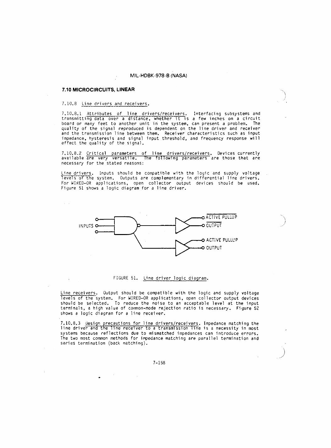
MIL-HDBK-978-B (NASA)
7.10 MICROCIRCUITS, LINEAR
7.10.8 Line drivers and receivers.
7.10.8.1 Attributes of line drivers/receivers. Interfacing subsystems and transmitting data over a distance, whether it is a few inches on a circuit board or many feet to another unit in the system, can present a problem. The quality of the signal reproduced is dependent on the line driver and receiver and the transmission line between them. Receiver characteristics such as input impedance, hysteresis and signal input threshold, and frequency response will effect the quality of the signal.
7.10.8.2 Critical parameters of line drivers/receivers. Devices currently available are very versati1e. HTe fol1 owing parameters are those that are necessary for the stated reasons:
Line drivers. Inputs should be compatible with the logic and supply voltage levels of the system. Outputs are complementary in differential line drivers. For WIRED-OR applications, open collector output devices should be used. Figure 51 shows a logic diagram for a line driver.
FIGURE 51. Line driver logic diagram.
Line receivers. Output should be compatible with the logic and supply voltage levels of the system. For WIRED-OR applications, open collector output devices should be selected. To reduce the noise to an acceptable level at the input terminals, a high value of common-mode rejection ratio is necessary. Figure 52 shows a logic diagram for a line receiver.
7.10.8.3 Design precautions for line drivers/receivers. Impedance matching the line driver and tne line receiver to a transmission line is a necessity in most systems because reflections due to mismatched impedances can introduce errors. The two most common methods for impedance matching are parallel termination and series termination (back matching).
7-158

MIL-HDBK-978-B (NASA)
7.10 MICROCIRCUITS, LINEAR
S T R O B E
FIGURE 52. Line receiver logic diagram.
Parallel termination is best suited for applications where there are many receivers for one driver, and the data is fairly symmetrical in nature. The terminating resistor, equal in value to the transmission line impedance, is placed across the transmission line at the furthest point from the driver.
Series terminaton can only be used when there is one receiver for every driver. The series resistor has such a value that its resistance plus the output resistance of the driver equal the transmission line impedance. This applies to the single-ended system. For the balanced differential system, each output of the driver has an external series resistance, which when added to its own output resistance, equals one half the impedance of the transmission line.
7.10.9 Timers.
7.10.9.1 Attributes of timers. Monolithic timing circuits are highly stable controllers capable of producing accurate time delays or oscillation. In the time delay mode of operation, the time is precisely controlled by one external resistor and capacitor. For a stable operation as an oscillator, the free running frequency and the duty cycle are both accurately controlled with two external resistors and one capacitor. The functional block diagram of a typical timer is shown in Figure 53.
Today different types of timers are available in single or dual versions, and in bipolar or CMOS technology. Applications for timers include missing pulse detectors, oscilloscope calibrators, darkroom enlarger timers, touch switches, basic square wave oscillators, alternating LED flashers, voltage-controlled oscillators, programmable voltage-controlled timers, frequency synthesizers and many others.
7-159

MIL-HDBK-978-B (NASA)
7.10 MICROCIRCUITS, LINEAR
RESET CONTROL
THRESHOL OUTPUT
TRIGGER •C
r \ DISCHARGE
GND
FIGURE 53. Timer functional block diagram.
7.10.9.2 Critical parameters of timers. General types of monolithic timers are available for use in linear and digital signal processing applications. The important parameters are as follows:
a. Timing control range nanoseconds to hours
b. Astable or monostable operating modes
c. Adjustable duty cycle
d. High output current
e. Output logic and supply voltage system compatabi1ity
f. Temperature stability over the full operating temperature range.
7.10.9.3 Design precautions for timers. Several precautions should be taken with respect to the power supply. TFe most important is good power supply filtering and bypassing. Voltage ripple on the supply line can cause loss of timing accuracy. A capacitor from the power supply to ground, ideally directly across the device, is necessary. The capacitance value will depend on the specific application. Values of from 0.01 \f to 10 mF are not uncommon. The capacitor should be as close to the device as physically possible.
If timing accuracy is to be maintained, stable external components are neces-sary. Most of the initial timing error is due to the inaccuracies of the external components. The timing resistors should be the metal film type if accuracy and repeatability are important design criteria. If the timing is critical, an adjustable timing resistor is necessary. A good quality multi-turn pot might be used in series with a metal film resistor to make up the resistive portion of the RC network.
7-160

MIL-HDBK-978-B (NASA)
7.10 MICROCIRCUITS, LINEAR
The timing capacitor should also be high quality, with very low leakage. Ceramic disc capacitors should not be used in the timing network under any circumstances. Several acceptable capacitor types are silver mica, Mylar, polystyrene, and tantalum.
If timing accuracy is critical over temperature, timing components with a small positive temperature coefficient should be chosen. The most important characteristic of the capacitor is low leakage. Obviously any leakage will subtract from the charge count causing the actual time to be longer than the calculated value.
The power dissipation of the package should never be exceeded. With extremely large timing capacitor values, a maximum duty cycle which allows some cooling time for the discharge transistor may be necessary.
7.10.10 Multipliers.
7.10.10.1 Attributes of multipliers. A four-quadrant multiplier with normal XY transfer function can also divide in two quadrants with a 10 V Z/X trans-fer function, and also perform square root and squaring functions. Selection of function in most cases may be accomplished with external passive components only.
In theory, a multiplier has an output which is ideally the product of two input variables, X and Y, divided by the 10-volt scaling voltage. However, the practical multiplier is subject to various offset errors and nonlinearities, which must be accounted for in its application.
As shown in Figure 54, the multiplier may be considered as having two parts; one contains the input circuitry and the multiplying cell and the other is the gain-conditioning operational amplifer, A.
r • X T , , M - -To" • F IX'X)
1
10 R
-VwV
X 0
J
FIGURE 54. Functional block diagram of typical multiplier.
7-161

MIL-HDBK-978-B (NASA)
7.10 MICROCIRCUITS, LINEAR
The "total error" specification includes the effects of all errors. Although a guide to performance, it may produce an excessively conservative design in some applications. For example, output offset is not important if the output is to be capacitively coupled or the initial offset is nulled. Gain error is not important if system gain is to be adjusted elsewhere in the system or if gain is not a critical factor in system performance. If frequent calibration of offset is possible and scale-factor errors are allowed, nonlinearity becomes the limiting parameter. In such cases, improvements in predicted error can be achieved by using the approximate linearity equation:
f (X, Y) = | V x| e x + I Vy | £y
where e x and £y are the specified fractional linearity errors and V x and Vy are the input signals.
Multipliers are used for modulation and demodulation, remote gain adjustment, power measurement, and mathematical operations in analog computing, curve fitting, and linearizing.
X or Y feedthrough is the output signal for any value of X or Y when no volts are applied to the other input, the value depends on test conditions, including frequency, temperature and applied signal amplitude.
7.10.10.2 Critical parameters of multipliers. The critical parameters of a multiplier are total error, feedthrough error, input common mode rejection ratio, and output offset voltage.
Total error: The sum of the effects of input and output dc offsets, nonlinear-ity and feedthrough. Feedthrough error is the sum of the effects of input offsets and nonlinearity.
Input common mode rejection ratio is the ratio of the input common mode voltage to the output error voltage. Larger values mean better rejection of common-mode signals and are therefore more desirable in applications where noise is a problem.
Output offset voltage is the offset voltage at the output amplifier stage. It is usually minimized during manufacture but varies with temperature.
7.10.10.3 Design precautions for multipliers. When selecting a multiplier, device parameters important in a given application must be considered. Atten-tion must be given to parameters which vary with temperature and power supply voltage. This information can be obtained from the data sheet.
All possible causes of output error must be taken into consideration in order to assure the required accuracy of the output.
7-162

MIL-HDBK-978-B (NASA)
7.10 MICROCIRCUITS, LINEAR
7.10.11 Phase locked loops (PLL).
7.10.11.1 Attributes of phase locked loops. Monolithic integration has changed the phase locked loop from a specialized design technique to a general-purpose building block. Today over a dozen different integrated PLL products are avail-able from a number of manufacturers. Some of these are designed as general-purpose circuits, suitable for a multitude of uses. Others are intended or optimized for special applications such as tone detection, stereo decoding, am detection, frequency synthesis, fm demodulation, frequency-shift keyed demod-ulation, signal conditioning, data synchronization, and motor speed control.
As a functional block, the primary purpose of a PLL is to compare an incoming signal with an internally generated reference signal in both the frequency and phase domain, and to compensate for any differences between the two by adjusting its internal references to match the input signal.
A simple block diagram of a PLL is shown in Figure 55. As can be seen from the figure, the basic elements of a PLL are a phase comparator, a low pass filter, and a voltage-control led- oscillator. The basic principle of operation of a PLL can briefly be explained as follows:
With no input signal applied to the system, the error voltage Vd is equal to zero. The voltage-controlled oscillator (VCO) operates at a set frequency (f 0) which is known as the free-running frequency. If an input signal is applied to the system, the phase comparator compares the phase and frequency of the infxut signal with the VCO frequency and generates an error voltage, V e(t), that is related to the phase and frequency difference between the two signals. This error voltage is then filtered and applied to the control terminal of the VCO. If the input frequency, f s , is sufficiently close to f 0 , the feedback nature of the PLL causes the VCO to synchronize, or lock, with the incoming signal. Once in lock, the VCO frequency is identical to the input signal, except for a finite phase difference.
7.10.11.2 Critical parameters of phase locked loops. Two key parameters of a PLL system are its lock and capture ranges. They are defined as follows:
Lock range: The range of frequencies around the fo over which the PLL can main-tain lock with an input signal. It is also known as the tracking or holding range. Lock range increases as the overall gain of the PLL is increased.
Capture range: The band of frequencies in the vicinity of f 0 where the PLL can establish or acquire lock with an input signal. It is also known as the acquisition range. It is always smaller than the lock range and is related to the low-pass filter bandwidth. It decreases as the bandwidth is reduced.
7.10.11.3 Design precautions for phase locked loops. The following is a dis-cussion of the key performance parameters associated with various applications.
7-163

MIL-HDBK-978-B (NASA)
7.10 MICROCIRCUITS, LINEAR
FIGURE 55. Basic diagram of a phase locked loop.
FM demodulation. There are three key parameters which should be examined:
a. Quality of demodulated output. This is normally measured in terms of the output level, distortion, and signal/noise ratio for a given fm deviation.
b. Voltage-controlled.' oscillator (VCO) frequency range and frequency stability. For reliable operation, the VCO upper frequency limit should be at least 20 percent above the fm carrier frequency. VCO frequency stability is important, especially if a narrow-band filter is used in front of the PLL, or multiple input channels are present. If the VCO exhibits excessive drift, the PLL can drift out of the input signal band as the ambient temperature range varies.
c. Detection threshold: This parameter determines the minimum signal level necessary for the PLL to lock and demodulate an fm signal of given elevation.
In most fm demodulation applications, it is also desirable to control the amplitude of the demodulated output.
Frequency-shift keyed (FSK) decoding. Frequency-shift keying used in digital communications is very similar to analog fm demodulation. Therefore, any PLL integrated circuit can be used for FSK decoding, provided that its input sensi-tivity and the tracking range are sufficient for a given FSK signal deviation. Some of the basic requirements and desirable features for a PLL used in FSK decoding are center frequency stability, logic compatible output, and control of VCO conversion gain. Center frequency stability is essential to ensure that the VCO frequency range stays within the signal band over the operating temperature range. A logic compatible output is desirable to avoid the need for an external voltage comparator to square the output pulses.
7-164

MIL-HDBK-978-B (NASA)
7.10 MICROCIRCUITS, LINEAR ) Frequency synthesis. This application requires a PLL circuit with the loop opened between the VCO output and the phase comparator input, so that an external frequency divider can be inserted into the feedback loop of the PLL.
Signal conditioning. Most signal conditioning applications require very narrow-band operation of the PLL. This in turn may require the use of active filters within the loop, i.e., between the phase detector and the VCO.
7.10.12 Physical construction and mechanical considerations. Construction and mechanical considerations of linear and special purpose circuits are generally the same as for other microcircuits. A vast majority of monolithic microcir-cuits are constructed with the planar diffusion process. Basic descriptions of fabrication, assembly, thermal characteristics, reliability and other details of semiconductor devices are given in the general subsection on transistors (5.1) and microcircuits (7.1).
7.10.13 Military designation. A description of the designation for military microcircuits are given in subsection 7.1 General, paragraph 7.1.32.
7.10.14 Environmental considerations. Environmental considerations of micro-circuits are included in subsection 7.1 General, paragraph 7.1.7 General relia-bility considerations.
V 7.10.15 Reliability considerations. Reliability considerations of linear and J special purpose microcircuits are generally similar to other microcircuits.
They are treated in subsection 7.1 General, paragraph 7.1.7 General reliability considerations. Derating is an important technique of increasing linear microcircuit reliability. MIL-STD-975 should be consulted for applicable derating factors for the various types of linear microcircuits.
/ 7-165

MIL-HDBK-978-B (NASA)
7.10 MICROCIRCUITS, LINEAR
7.11 Hybrid.
7.11.1 Introduction. A hybrid microcircuit is a microelectronic device that uses a combination of active and passive circuit elements from more than one technology. Circuit functions can be implemented in hybrid form that offers an economic and technical advantage over the same function implemented in mono-lithic form. Hybrid microcircuits are divided into three general categories.
i a. Multichip hybrid microcircuits. The multichip hybrid microcircuit
is defined as a device that contains several active elements mounted on a header with no thin- or thick-film associated circuitry.
b. Simple hybrid microcircuits. The simple hybrid microcircuit is more complex than the multichip version and consists of one or more active and passive elements mounted and interconnected by deposited metalli-zation on a single layer substrate. It may also have thin- or thick-film resistors deposited on the substrate. Military specification MIL-M-38510 defines the package inner-seal perimeter of simple hybrid microcircuits as not exceeding 2 inches.
c. Complex hybrid microci rcuits. Complex hybrid microcircuits contai n the same basic combination of active and passive elements as the simple hybrid microcircuits except that the number and complexity of the elements is greater and the substrate may consist of several conducting layers. The package inner seal perimeter of the complex hybrid is defined as greater than 2 inches.
Compared with monolithic devices, the design costs of hybrids are relatively small. Minor changes readily can be made to an existing design to optimize a hybrid device for an application. Although some standard circuits are marketed, most hybrid devices are at least partially custom designed. Custom designing provides hybrid microcircuits with a performance advantage, but at some expense of reliability assurance because high volume production of any one design is seldom achieved.
Hybrid microcircuits will continue to be a major factor in new system designs even though monolithic devices continue to expand to higher levels of complexity and encompass functions previously' avai lable only in hybrid form. Continued use of hybrid microci rcuits will be accomplished through the use of the new, more complex monolithic dice into even more complex hybrid microcircuits, thus allowing hybrid circuits to remain at the forefront of microcircuit technology.
7.11.2 Usual applications. Although nearly any integrated circuit can be made in hybrid form, those tFat provide characteristies or functions beyond the present capabilities of monolithic devices are of great interest for aerospace applications. Monolithic devices are generally preferred for applications within their capabilities because of their greater anticipated reliability and economy and, sometimes, smaller size.
7-166

MIL-HDBK-978-B (NASA)
7.10 MICROCIRCUITS, LINEAR
Some microcircuits would be impossible to implement in monolithic form, but may be easily realized with a hybrid design. For example, circuits requiring large capacitances or resistor networks are easily fabricated in hybrid form. Hybrid microcircuits are often called for when power, high frequency, or close toler-ance circuit elements are required. Some specialized hybrid circuits use the thermal coupling between semiconductors in close proximity to provide controls not found in discrete circuits, such as a corrective feedback to prevent thermal runaway.
Typical systems applications of hybrid microcircuits include control, display, power, transmitter, receiver, and signal processor circuits. Hybrid micro-wave integrated circuits are normally used as receivers, mixers, transmitters, phase comparators, and levelers. A hybrid microcircuit can be designed and prototype hardware delivered in four to six months. By comparison, development of a custom monolithic circuit may require 12 months for delivery of prototype samples. Hybrid packages are ideally suited to consolidate SSI and MSI chips into small physical volumes with high electronic capability.
7.11.2.1 Available functional types. A large variety of hybrids are available off-the-shelf. Some of the functional applications of standard hybrids are in digital signal processing, operational amplifiers, voltage references, analog multiplexers, sample-and-hold amplifiers, D/A and A/D converters, flash con-verters, and data acquisition systems. Custom hybrids may be obtained to these products and to such applications as voltage to frequency converters* instru-mentation amplifiers, modulators, filters, analog switches, bus interface, analog and digital interface, and thin-film resistor networks.
7.11.2.2 Comparative attributes of packages. A large variety of hybrid pack-ages are used in aerospace - applications. The major package types are: lead-less, plug-in bathtub or uniwall, the all-metal power-package, beryl 1ia-base power-package, platform, and flatpack. Figure 56 shows four typical package types. The standard flatpack is the most common. Figure 57 shows the general features of a flatpack package and Figure 58 displays details of the package cross-section.
All package types are available in a wide range of sizes and lead count. For example, the flatpack comes in sizes from approximately 0.6 x 0.6 inch to 2 x 2 inch length and width, and lead counts of 20 to approximately 120. Table XXXIV is a comparison of advantages and disadvantages of six major hybrid package types. The choice of package will depend on the design constraints imposed on the hybrid such as high-wattage elements, minimum board area, and high lead count, etc.
7-167

MIL-HDBK-978-B (NASA)
7.10 MICROCIRCUITS, LINEAR
FLATPACK BERYLLIA BASE PACKAGE
PLATFORM
n IT
BATHTUB
FIGURE 56. Four common hybrid package types without covers,
7-168

MIL-HDBK-978-B (NASA)
7.10 MICROCIRCUITS, LINEAR
SUBSTRATE TO POST, CAPACITOR, AND RESISTOR CHIP CONNECTIONS ARE MADE USING 2-MIL GOLD WIRE OR 1-BY-3-MIL RIBBON
1-MIL-DIAMETER WIRE BONDED TO SEMICONDUCTOR CHIP AND SUBSTRATE FILM CONDUCTOR
GOLD-PLATED KOVAR LID
SUBSTRATE, CAPACITORS AND RESISTOR CHIPS ATTACHED BY NON-CONDUCTIVE ADHESIVE
GOLD-PLATED KOVAR METAL BASE PACKAGE
HERMETIC FINAL SEAL MADE BY WELDING
GOLD-PLATED KOVAR LEADS WITH GLASS TO METAL SEAL
i SEMICONDUCTOR CHIPS ATTACHED BY CONDUCTIVE ADHESIVE
FIGURE 57. General features of a flatpack hybrid microcircuit.
CAPACITOR CHIP
THERMOCOMPRESSION BOND
KOVAR LID
ULTRASONIC TC BOND \ ALUMINUM jq WEDGE
WIRE \ BALL G 0 L D BOND G 0 L D \ O N D v W » * E
WIRE \ v
• HERMETIC SEAL (WELD)
CHIP
ALUMINA SUBSTRATE
PACKAGE BASE
PACKAGE LEAD
FIGURE 58. Cross-section of a hybrid substrate packaged in a flatpack.
7-169

MIL-HDBK-978-B (NASA)
7.9 MICROCIRCUITS, MICROPROCESSORS
TABLE XXXIV. Comparison of characteristics of common hybrid packages
Type i
Characteristics
Leadless pack-ages
Advantages
Di sadvantages
Ceramic with inetal ring frame for weldable covers and castellated leads
No glass-to-metal seal, uses less PWB area
Because of thermal expansion these packages can only be used with ceramic PWBs. Connections can only be made using solder. It is difficult to inspect the connection and to remove the case from the PWB.
Plug-in bathtub
Advantages
Di sadvantages
Uniwall metal base with sidewalls and pins on two, three, or four sides, preferred to platform packaging for new designs.
Packages can be welded using automated techniques. Parts can be opened and resealed.
Some attention must be given to device positioning, especially for active elements that are to be wedge- or aluminum-wire bonded so that bonding tool tip clearances are satisfied. Domed lids must usually be special-ordered. Packages cannot be repaired if the pins are fractured near the package walls or if the glass beads crack. When plug-in packages are removed from module boards, package herme-ticity is lost if glass beads around the package pins are damaged during removal; the hybrid then needs repackaging.
Metal power packages
Advantages
Disadvantages
Copper, Kovar, or molybdenum power packages with weldable lids.
Best for heat dissipation in power circuits. (NOTE: Kovar is not as good as beryllia, described elsewhere).
Require special process and equipment. They are heavy and usually are custom designed. Also, they are expensive and difficult to seal.
7-170

MIL-HDBK-978-B (NASA)
7.10 MICROCIRCUITS, LINEAR
TABLE XXXIV. Comparison of characteristics of common hybrid packages (continued)
Type Characteristics
Beryl 1ia-base power-package
Advantages
Disadvantages
Metal ring frame soldered to a beryllia base
Used when the heat generated by high-wattage elements in a hybrid must be more efficiently dissipated than is possible using alumina or all-metal packages. A number of different beryl 1ia-base thicknesses are available. Packages can be sealed using flat or domed lids. Sealing can be done by welding or soldering.
Though sealed packages can be opened and resealed, the oper-ation is not as repeatable, and is therefore more expensive than when using all-metal packages. This is because the glass beads in the ring frame of the beryllia package are less likely to withstand repeated thermal and mechanical stresses. Beryllia is toxic and requires special handling and processing.
Plug-in platform
Advantages
Oi sadvantages
Flat metal base with pins on two, three, or four sides. This is not recommended for new designs.
Because there are no sidewalls, wire bonding near the edge of the substrate is not a problem. Domed lids of different heights are available. Sealed packages can be opened and resealed.
The configuration is sealed by hand soldering. There is some possibility of solder-ball formation, especially with long (>1.5-inch) packages. If pins are fractured or if the glass beads around the pins crack, the package cannot be repaired. Package hermeticity is lost if glass seals around the pack-age pins are damaged when the package is removed from module boards. The hybrid then needs repackaging.
Flatpack
Advantages
Disadvantages
Metal ring frame brazed to a metal base or uniwall con-struction. Radial leads on two, three, or four sides.
Packages can be sealed by welding. Step or flat lids are normally used, but domed lids are available so that larger elements can be incorporated. These packages can be opened and resealed.
Leads fractured near package walls or cracked glass beads around these leads cannot be repaired.
7-171

MIL-HDBK-978-B (NASA)
7.10 MICROCIRCUITS, LINEAR
7.11.3 Physical construction. Construction of hybrid devices begins with a substrate on which the circuit is built. This substrate is usually an alumina-AI2O3 ceramic which provides a good combination of electrical insulation and heat conduction properties.
Selection criteria for various substrates are summarized in Table XXXV.
TABLE XXXV. Substrate selection criteria
Substrate Comment
Unglazed alumina Normally preferred for thick- and thin-film circuits.
Polished alumina, sapphire
Preferred for microwave circuits.
Ground alumina Preferred for multilayer and large-area thick-film circuits.
Beryl lia High-power dissipation; can be used as a mother board for alumina substrates.
In applications where superior heat transfer properties are required, (e.g., due to the use of power transistor dice), a suitable substrate material is beryllia [beryllium oxide (BeO)]. However, a word of caution is necessary concerning the use of beryllia. This substrate is extremely poisonous under certain conditions. It should not be ground, filed, machined, or otherwise abraded. Exposure to high temperature (above 250 °C) is also to be avoided. Airborne particles and fumes which are released under the above conditions are lethal.
Microwave hybrid microcircuit designs are optimized by the use of sapphire sub-strates. Although this may be more expensive, its use can be justified by the superior performance which is achieved. Parameters which are significantly improved through the use of sapphire are intermodulation distortion (crosstalk) and noise figure.
7-172

MIL-HDBK-978-B (NASA)
7.10 MICROCIRCUITS, LINEAR
Conductors, insulating layers, and passive elements are deposited on the sub-strate using thin-film or thick-film techniques. Semiconductor dice are gener-ally attached to gold pads by means of silicon-gold eutectic bonding, although other techniques, such as epoxy and Teflon as well as beam lead bonding are sometimes used. Interconnection of semiconductor bonding pads, passive ele-ments, and external leads is usually accomplished by gold wire using ball bonding (see Figure 59 for a typical construction).
FIGURE 59. Comparison of schematic diagram and typical construction of a hybrid microcircuit.
7-173

MIL-HDBK-978-B (NASA)
7.10 MICROCIRCUITS, LINEAR
Although hybrid microcircuits allow use of circuit elements with much closer tolerances than those provided by monolithic circuits, close tolerances of the completed circuit are not always easily achieved. As with diffused resistors, the film resistors as deposited provide a better matching of resistances and temperature coefficients than tolerances on absolute values. They may, how-ever, be trimmed to much closer tolerances by means of power pulses, abrasion, or laser trimming. More complex circuits which use many semiconductor dice may suffer degradation of parameters as a result of long exposure at the high temperatures encountered in die bonding and wire bonding.
The development of the leadless chip carrier and the increasing availability of circuit elements in this form is of significant value to the manufacturer of complex hybrid microcircuits. Utilization of circuit elements packaged in the chip carriers allows 100-percent reliability screening prior to installa-tion in a hybrid microcircuit, a distinct advantage over unpackaged dice which historically have caused electrical and/or environmental yields as low as 60 percent in the finished hybrid microcircuit. Chip carriers are hermetically sealed and also lend themselves to automated assembly techniques, thus simpli-fying hybrid microcircuit assembly and processing.
7.11.3.1 Thin-film. Thin-film circuits are made by vapor deposition of con-ductors, resistors, and dielectrics through a metal mask in a vacuum chamber (selective etching may be used as an alternative). Conductor patterns are generally gold, although aluminum may be used. Nichrome resistors with sheet resistance up to 300 a/square and cermet resistors with sheet resistance up to 5000 Q/square are the most widely used types, although other metals such as tantalum and titanium may be used. Thin-film capacitors using silicon monoxide or silicon dioxide as the dielectric may be used for smaller values, but they require too much area for values greater than about 100 pF. For larger values, discrete types such as ceramic chip capacitors are used.
See summary of thin-film element characteristics in Table XXXVI.
7.11.3.2 Thick-film. Thick-film circuits are most generally produced by apply-ing metallic and insulating pastes to the substrate through screening masks. Each application is followed by a pass through an oven to set the paste and to bond it to the substrate. Gold paste is generally used for the conductor pattern. Resistor pastes, which are generally proprietary formulations, come in a wide range of sheet resistivities. Capacitors may be made to values as high as 10,000 pF by thick-film techniques or discrete capacitors may be used. A protective glass coating is generally applied to the entire circuit as a final step. For additional circuit characteristics, see summary of thick-film element characteristics in Table XXXVI.
7-174

MIL-HDBK-978-B (NASA)
7.10 MICROCIRCUITS, LINEAR
TABLE XXXVI. Thin-film and thick-film characteristics
Material Comment
Thin-film conductors
These are used when high-density, single-layer packaging is required. They allow narrower lines and spacing than are possible with thick-film conductors.
Thin-fi lm resistors
These can be etched from thin-film conductor substrates. They are used for values up to 20 kft (and in some instances up to 100 kft) and for dynamic trimming to tight tolerances. These resistors are limited to the lower values because only relatively low sheet resistivities are available.
Thick-film conductors
They are less expensive than thin-film conductors, espe-cially when many single-layer, conductor-only substrates are involved. Conductor lines and spaces are not as narrow as those possible with thin-film, so some packaging density is lost. Packaging density can sometimes be improved by redesigning a dense, single-layer thin-film circuit to take advantage of the thick-film multilayer concept "
Thick-film resistors
A wide range of resistor values can be obtained by select-ing from a range of sheet resistivities that vary from 1 ft to more than 1 Mft per square. Often, chip resistors are used in hybrids to take advantage of their high resistivities and relatively low demands for space on the substrate. These resistors can be dynamically trimmed but it is not recommended.
7.11.3.3 Die requirements. Microcircuits and semiconductor die used for con-struction of class S or class B hybrids shall meet the screening and quality conformance provisions of Method 5008 of MIL-STD-883 for the appropriate reliability class.
7.11*3.4 Specification of passive elements and packages. Passive elements and packages used in the construction of class S and class B hybrids shall meet all quality and reliability requirements listed under class S or class B , respec-tively, as specified in Appendix G of MIL-M-38510 and further detailed in Method 5008 of MIL-STD-883.
7-175

MIL-HDBK-978-B (NASA)
7.10 MICROCIRCUITS, LINEAR
7.11.4 Military designation. Quality and reliability assurance requirements for class S and class B hybrid microcircuits are called out in Appendix G in the General Specification for Microcircuits (MIL-M-38510). NASA quality levels of Grade 1 and Grade 2 are satisfied by class S and class B , respectively. Implementation of the requirements of Appendix G is detailed in Method 5008 of MIL-STD-883, Test Methods and Procedures for Microelectronics. Method 5008 establishes the detailed screening and quality conformance procedures for achieving class S and class B levels for microcircuits, semiconductors, passive elements, and packages used for hybrid construction and should be strictly satisfied for NASA hybrid applications. A further description of NASA Standard Parts Program and the designation for military microcircuits are given in subsection 7.1 General.
7.11.5 Electrical characteristics. Most hybrid microelectronic . devices' are custom made for their particular applications. However, the part operation should be precisely defined by a table of electrical characteristies which includes all necessary parameters with test conditions, parameter minima and maxima, parameter typical values, and associated symbols with units. Electrical characteristics should also include areas such as a functional diagram, a block diagram, a table of pin assignments, a mechanical outline, and a table of absolute maxima ratings. A worst-case circuit design analysis should be per-formed following the requirements of Appendix G of MIL-M-38510.
All active and passive elements of the hybrid should have electrical charac-teristics derated according to the appropriate derating factors listed in MIL-STD-975 for NASA standard parts. Derating will increase the safety margin between the operating stress level and the actual failure level for the con-stituent hybrid parts and will provide added protection for system anomalies unforeseen by the applications engineer.
7.11.5.1 Special testability considerations. Special care should be taken in hybrid applications to ensure that the device is testable. Ideally, built-in test procedures should be incorporated to set the state of all elements of the hybrid and to observe such states. The hybrid designer should anticipate and allow for test equipment and system test limitations when designing built-in test features. Test time should be minimized, because test machine time may sometimes cost more than the part itself. Extra test pins are sometimes needed to adequately test a hybrid part.
7.11.5.2 Thermal design considerations. A thermal design analysis should be performed on the hybrid following the conditions of Appendix G of MIL-M-38510. All active and passive elements of the hybrid should be derated to worst-case conditions.
All active and passive elements in hybrids should be, as a minimum, derated to the requirements of MIL-STD-975.
Hybrid manufacturers shall comply with the facilities and manufacturing line requirements of MIL-STD-1772.
7-176

MIL-HDBK-978-B (NASA)
7.10 MICROCIRCUITS, LINEAR
7.11.6 Environmental considerations. NASA hybrids typically have demanding environmental requirements. Extremes in environmental tolerance arise from maximum operating limits of temperature-sensitive chip elements, electrical performance, power dissipation, vibration and shock, and radiation. Environ-mental test requirements are satisfied, except for radiation, by the class S requirements of Table VII of Method 5008, MIL-STD-383. Radiation testing of the constituent microcircuit and semiconductor die of class S hybrids should be done following the requirements of Table III of Method 5008.
7.11.7 Reliability consideration. Hybrid microcircuits for NASA Grade 1 or 2 applications require class S or B quality and reliability assurance levels. Appendix G of MIL-M-38510 details the procedures for documenting the requir-ements for such hybrids. Appendix G references method 5008 of MIL-STO-883 to describe the hybrid device evaluation procedures to implement these require-ments. The hybrid device evaluation has four general requirements: element evaluation, process control, device screening, and quality conformance evalua-tion. These requirements should be satisfied at the class S quality level for NASA Grade 1-type applications. For Grade 2 NASA applications, the hybrid device evaluation must satisfy the class B quality level.
7-177

MIL-HDBK-978-B (NASA)
7.10 M I C R O C I R C U I T S , LINEAR
THIS PAGE INTENTIONALLY LEFT BLANK
7-178

INSTRUCTIONS: In a continuing effort to make our standardization documents better, the DoD provides this form for use in submitting comments and suggestions for improvements. All users of military standardization documents are invited to provide suggestions This form may be detached, folded along the lines indicated, taped along the loose edge (DO NOT STAPLEh and mailed In block 5, be as specific as possible about particular problem areas such as wording which required interpretation, was too rigid restrictive, loose, ambiguous, or was incompatible, and give proposed wording changes which **»uld alleviate the problems Enter in block 6 any remarks not related to a specific paragraph of the document. If block 7 is filled out. an acknowledgement will be mailed to you within 30 days to let you know that your comments were recetved and are being considered.
NOTE: This form may not be used to request copies of documents, nor to request warv^rs, deviations, or clarification of specification requirements on current contracts. Comments submitted on this form do not constitute or imply authorization to waive any portion of the referenced document/*/ or to amend contractual requirements.
(fom atong tfm
tfoU along tfm Mrml
National Aeronautics and Space Administration Washington, QC. 20546 Official Business fenalty tor Private Use $300
BUSINESS REPLY MAIL FIRST CLASS PERMIT MO. U B S WASHINGTON. DjC.
NO POSTAGE NECESSARY W MAILED
IN THE UNITED STATES
POSTAGE WIU. BE MUD ST NASA
Goddard Space Right Canter National Aeronautics and Space Administration Attn: 311.A Graanbatt Maryland 20771
IVJASA

i £
1
K S 0
1 1
s Uj Q £
STANDARDIZATION DOCUMENT IMPROVEMENT PROPOSAL (See Instructions — Reverse Side)
1 DOCUMENT NUMBER 2. DOCUMENT TITLE
3a. NAME OF SUBMITTING ORGANIZATION 4 TYPE OF ORGANIZATION (Msr* on*/ n VENDOR
O U S E R
b. ADDRESS (Street, City, State, Zip Code) P I MANUFACTURER
5. PROBLEM AREAS a. Paragraph Number and Wording
b. Recommended Wording
c. Reason/Rationale for Recommendation
6. REMARKS
7a. NAME OF SUBMITTER (Last, First, MI) - Optional WORK TELEPHONE NUMBER (Inch** Am*
c. MAIUNG AOORESS tSemt. Ory. Son 27* Cod*/ - Opoontf & DATE OF SUBMISSION 1YYMMDD)
D D e £ ? i t 1 4 2 6 PREVIOUS EDITION IS OBSOLETE.

i

r
ii J ' f