microwave and optical engineering - rajiv gandhi … year/ec t71-moe/unit 1.pdf · rajiv gandhi...
TRANSCRIPT
RAJIV GANDHI COLLEGE OF ENGINEERING AND TECHNOLOGY
PONDY-CUDDALORE MAIN ROAD, KIRUMAMPAKKAM-PUDUCHERRY
DEPARTMENT OF ECE
EC T71 - MICROWAVE AND OPTICAL ENGINEERING
IV YEAR A – Mr.L.ARUNJEEVA., AP/ECE
IV YEAR B – Ms.R.JAYASHRI., AP/ECE
1
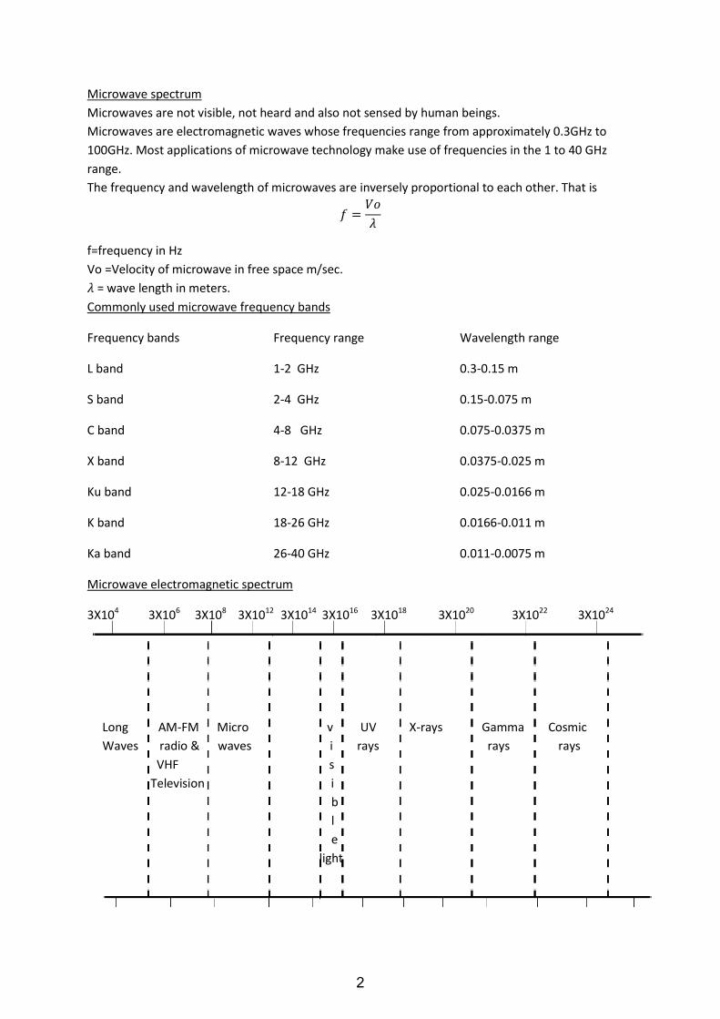
Microwave spectrum
Microwaves are not visible, not heard and also not sensed by human beings.
Microwaves are electromagnetic waves whose frequencies range from approximately 0.3GHz to
100GHz. Most applications of microwave technology make use of frequencies in the 1 to 40 GHz
range.
The frequency and wavelength of microwaves are inversely proportional to each other. That is
f=frequency in Hz
Vo =Velocity of microwave in free space m/sec.
= wave length in meters.
Commonly used microwave frequency bands
Frequency bands Frequency range Wavelength range
L band 1-2 GHz 0.3-0.15 m
S band 2-4 GHz 0.15-0.075 m
C band 4-8 GHz 0.075-0.0375 m
X band 8-12 GHz 0.0375-0.025 m
Ku band 12-18 GHz 0.025-0.0166 m
K band 18-26 GHz 0.0166-0.011 m
Ka band 26-40 GHz 0.011-0.0075 m
Microwave electromagnetic spectrum
3X10⁴ 3X10⁶ 3X10⁸ 3X10¹² 3X10¹⁴ 3X10¹⁶ 3X10¹⁸ 3X10²⁰ 3X10²² 3X1024
Long AM-FM Micro v UV X-rays Gamma Cosmic
Waves radio & waves i rays rays rays
VHF s
Television i
b
l
e
light
2
104 102 1 10-2 10-4 10-6 10-8 10-10 10-12 10-14 10-16
10-17
Characteristics of microwave
1. Frequency is high and wavelength is small.
2. They propagate in free space freely (means that attenuation in free space is small).
3. They are transmitted through good dielectrics (insulators).
4. They are reflected from good conductors (means that they do not penetrate in good conductors).
5. They consist of electric and magnetic fields which are perpendiculars to each other.
The electric and magnetic fields of microwaves in free space is related by
|
ηo =120 Ω
E=electric field
H=magnetic field
ηo=intrinsic impedance (or) characteristic impedance of free space
6. The power how by microwave is
P=ExH
P-instantaneous power flow (or) poynting vector
7. Microwaves carry power in free space like current carries power through transmission lines. But
the microwaves and current have opposite characteristics. The microwaves propagate in insulators
but current does not propagate.
8. microwaves lead to atomic and molecular resonant characteristics in several substances.
Advantages of microwaves
1. Large bandwidth
2. High directivity of microwave radiation pattern.
3. Antennae size becomes small and low fading effect.
4. Propagate through ionosphere provide effective satellite communication.
5. Effective for radar communication.
6. Effective for radiation therapy application.
7. Effective for TV transmission and reception.
Applications
1. To communicate efficiently between two points, it is important that the transmitted signal be
sharply focused and aimed at the receiving antennae. Since microwave frequencies have this ability
they are ideally suited for wireless type point to point communication.
2. The combination of satellites and point to point microwave transmission results in the ability to
communicate between continents.
3. In radar system microwaves are used to detect aircraft, guide supersonic missiles, observe and
traffic weather patterns and control flight traffic at airports.
4. The heating properties of microwave power is useful in a wide variety of commercial and
industrial application. The microwave oven is well known example.
3
“Microwave oven operates at a frequency of 2.45 GHz. Microwave oven is a domestic kitchen
electronic unit which is useful for cooking food quickly”
5. Medical applications – the possibility of exposing malignant cells to microwave heat is being
investigated as method of treating cancer.
6. Microwaves are used into radio astronomy to study radiation from and the stars.
7. Microwaves are also used in passive navigational aid to ship at sea.
8. Many substances exhibit atomic and molecular resonance in the microwave range. The analysis
and interpretation of these resonances, called microwave spectroscopy is an important vehicle in
the scientific effort to understand the fundamental nature of solids liquids and gases.
UNIT-I
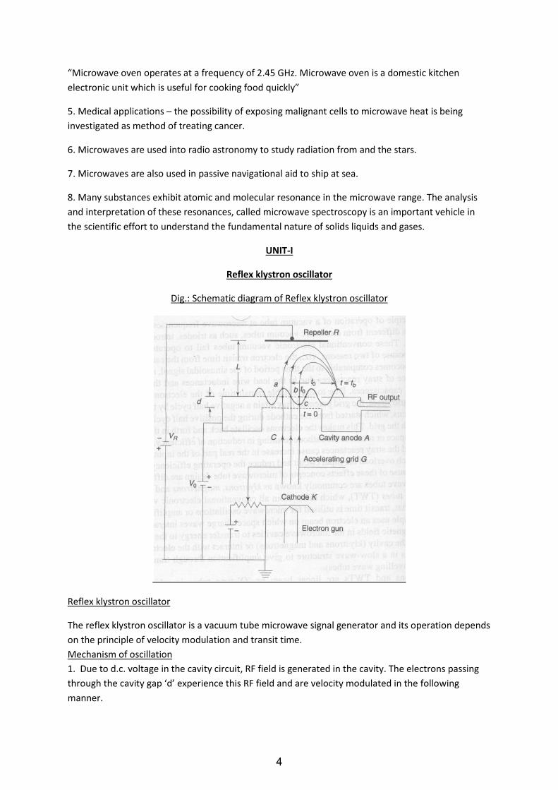
Reflex klystron oscillator
Dig.: Schematic diagram of Reflex klystron oscillator
Reflex klystron oscillator
The reflex klystron oscillator is a vacuum tube microwave signal generator and its operation depends
on the principle of velocity modulation and transit time.
Mechanism of oscillation
1. Due to d.c. voltage in the cavity circuit, RF field is generated in the cavity. The electrons passing
through the cavity gap ‘d’ experience this RF field and are velocity modulated in the following
manner.
4
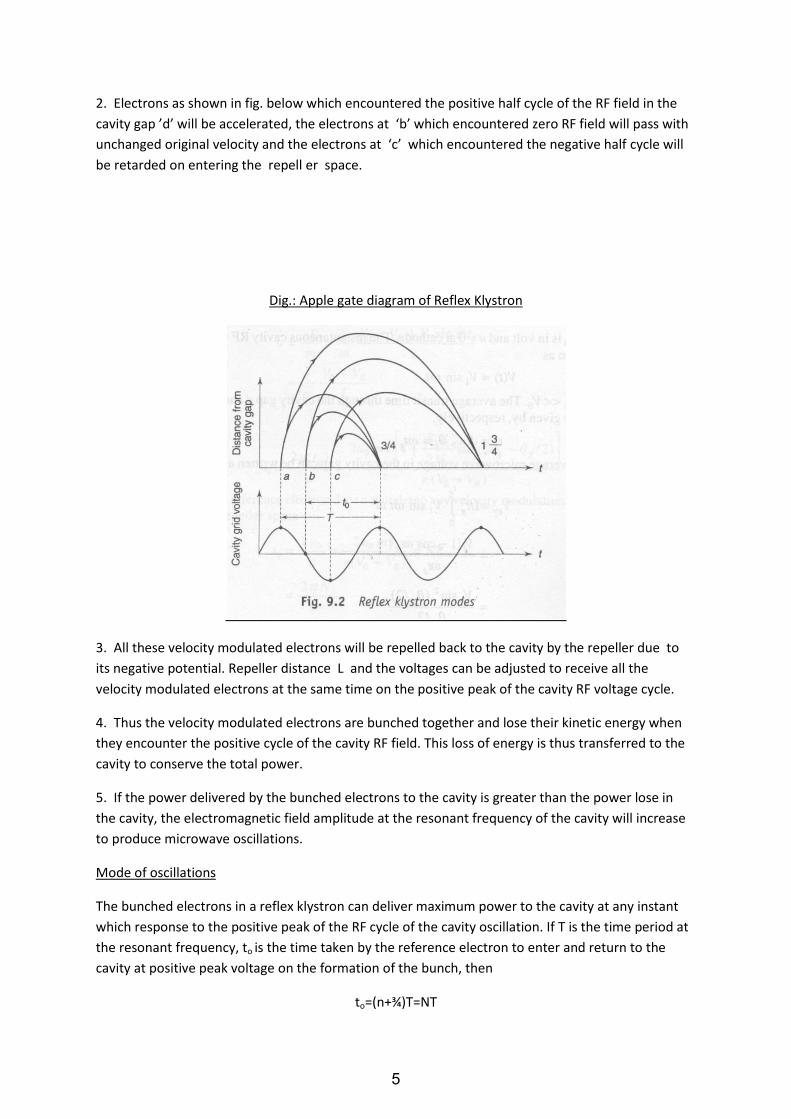
2. Electrons as shown in fig. below which encountered the positive half cycle of the RF field in the
cavity gap ’d’ will be accelerated, the electrons at ‘b’ which encountered zero RF field will pass with
unchanged original velocity and the electrons at ‘c’ which encountered the negative half cycle will
be retarded on entering the repell er space.
Dig.: Apple gate diagram of Reflex Klystron
3. All these velocity modulated electrons will be repelled back to the cavity by the repeller due to
its negative potential. Repeller distance L and the voltages can be adjusted to receive all the
velocity modulated electrons at the same time on the positive peak of the cavity RF voltage cycle.
4. Thus the velocity modulated electrons are bunched together and lose their kinetic energy when
they encounter the positive cycle of the cavity RF field. This loss of energy is thus transferred to the
cavity to conserve the total power.
5. If the power delivered by the bunched electrons to the cavity is greater than the power lose in
the cavity, the electromagnetic field amplitude at the resonant frequency of the cavity will increase
to produce microwave oscillations.
Mode of oscillations
The bunched electrons in a reflex klystron can deliver maximum power to the cavity at any instant
which response to the positive peak of the RF cycle of the cavity oscillation. If T is the time period at
the resonant frequency, to is the time taken by the reference electron to enter and return to the
cavity at positive peak voltage on the formation of the bunch, then
to=(n+¾)T=NT
5

N=n+¾, n=0, 1, 2…
The mode of oscillation is named as n=3/4 ,1 ¾ ,2 ¾ … for models n=0,1,2,3 respectively. The lowest
order mode ¾ occurs for a maximum value of repeller voltage. Higher modes occur at lower repeller
voltages. Since at the highest repeller voltage the acceleration of the bunched electrons of return is
maximum, the power output of the lowest mode is maximum.
The frequency of oscillations is controlled by the cavity dimensions and reflector voltage.
Analyses of reflex klystron
The electron velocity ‘u’ attained due to the d.c. beam voltage Vo is given by
u=µo=√ ---------(1)
u=5.93x10⁵√ m/s ---------(2)
the instantaneous RF voltage can be written as
V(f)=V1sinωt ---------(3)
V1<<V0 (beam voltage)
Average transit time (tg)=
i.e. average transit means time taken by the electron beam passes through the cavity gap ‘d’.
tg=
-----------(4)
transit angle θ=ωtg ------------(5)
The average microwave voltage in the cavity can be written as
Vav =
∫
dt ----------(6)
=
=
=
Vav=V1 β1 sin -----(7)
The factor β1 is called beam coupling co efficient of the cavity gap.
The exit velocity from the cavity gap after velocity modulation is given by
u(tg)=√
6
=√ (
)
Take Vo outside.
=√ (
)
=√ (
)
The factor
modulation if the modulated amplitude is <<1 then u(tg) is
u(tg)= (
)
u(tg)= (
) ------------(9)
Transit time
The round trip transit time tr in the repeller space is given by
tr=2
The factor 2 in the numerator arises because of the to and fro journey. The electron acceleration is
given by
a=eE/m =
is very less compared to Vo hence
a=
-----(10)
substitute u(tg)
tr=
( (
)
)
-----------------(11)
since the reference electron does not undergo any velocity modulation its transit time in repeller
space is
t0=
=
=NT
t0=
equation (11) can be written as
tr=t0( (
)
) ---------------------(12)
Density modulation and beam current
The time of arrival of electron to the cavity gap can be expressed by
7
tb=tg+tr
tb=tg+ t0( (
)
)
tb=tg+
(
)
tb=tg+
(
)
--------------------(13)
where X=
called the bunching parameter of reflex klystron
Bunched beam current ib
Bunched electron constitutes beam current ib
ib=
---------------------------(14)
to find
:
differentiate (13) w.r.t. tg
=(1+Xcos
))----------------------(15)
Equation (14) is
ib=
ib=
-1---------------(16)
we know that V1<<V0 and bunching parameter X=
since V1 is very small neglect X in the above equation
tb=tg+
------------------(17)
tg=tb -
tg=
ωtg=
hence (16) can be written as ib=
-1------------------(17)
by Fourier expansion the beam current of a reflex Klystron oscillator is
ib=I0+2I0∑ Jn(nX)
-------------(18)
β1ib=β1I0 + 2β1I0 J1(X) (
) ∑
----(19)
I term II term III-term
I term – dc component
II term – fundamental ac component
III term – harmonics
The klystron is generally tuned to fundamental ac component.
Ib=2 I0 J1(X) cos(ωtb-2𝝅N-θg/2)
This is the expression of the beam current induced in the cavity gap
The RF current induced in the cavity by the modulated electron beam (or) due to injected beam is
given by
IRF=β1ib
where β1 is the beam coupling co efficient of the cavity
8
IRF=β12 I0 J1(X) cos(ωtb-2𝝅N-θg/2) -------------------------(20)
Take ω common and neglect tg/2
IRF=β12 I0 J1(X) cos(ωtb-2𝝅N) -------------------------------(20)
This is the expression for induced RF current in the cavity.
Power output
The magnitude of the fundamental RF current in the cavity is given by
|iRF|=2Io β1 J1(X)
The rms RF power delivered to the cavity is
PRF=
PRF=
-----------------(20)
From bunching parameter X expression X=
the above equation can be written as
PRF=
-----------------------------(21)
Efficiency
The dc power supplied by the beam voltage Vo is
Pdc=VoIo
The electronic efficiency of reflex klystron oscillator is
η=
=
=
where N=n+3/4 where n=0,1,2,3…
from the Bessel function table X J1(X) attains a maximum value of 1.252 at X=2.408
thus the optimum values are
PRF=
η=1.252/𝝅N
η=0.3986/N
it has been observed that it is not possible to get ¾ mode but 1 ¾ leads the maximum RF power
output and efficiency
PRF max=
Efficiency is ηmax =22.7%
Two cavity klystrons
9

The two cavity reflex klystron is a widely used microwave amplifier operated by the principle of
velocity modulation and current modulation
Dig.: Schematic diagram of two cavity Reflex klystron oscillator
Mechanism of operation
1. All the electrons injected from the cathode arrive at the first cavity with uniform velocity. These
electrons passing at the cavity gap at zeros of the gap voltage(or) signal voltage pass through
unchanged velocity.
2. Those passing through the positive half cycles of the gap voltage undergo an increase in the
velocity.
3. Those passing through the negative swings of the gap voltage undergo a decrease in velocity. As
the result of these actions, the electrons gradually bunch together as they travel down the drift
space is known as velocity modulation.
4. The electron beam modulated to form bunches (or) undergoes density modulation in accordance
with the input RF cycle.
5. While passing through the catches cavity grid, this density modulated electron beam induces RF
current in the output cavity and thereby excite the RF field in the output cavity at input signal cycle.
6. The phase of field in the output cavity is opposite to that of the input cavity so that the bunched
electrons are retarded by the output gap voltage. The loss of kinetic energy of the electrons on
retardation process transfers RF energy to the output cavity continuously at signal.
10
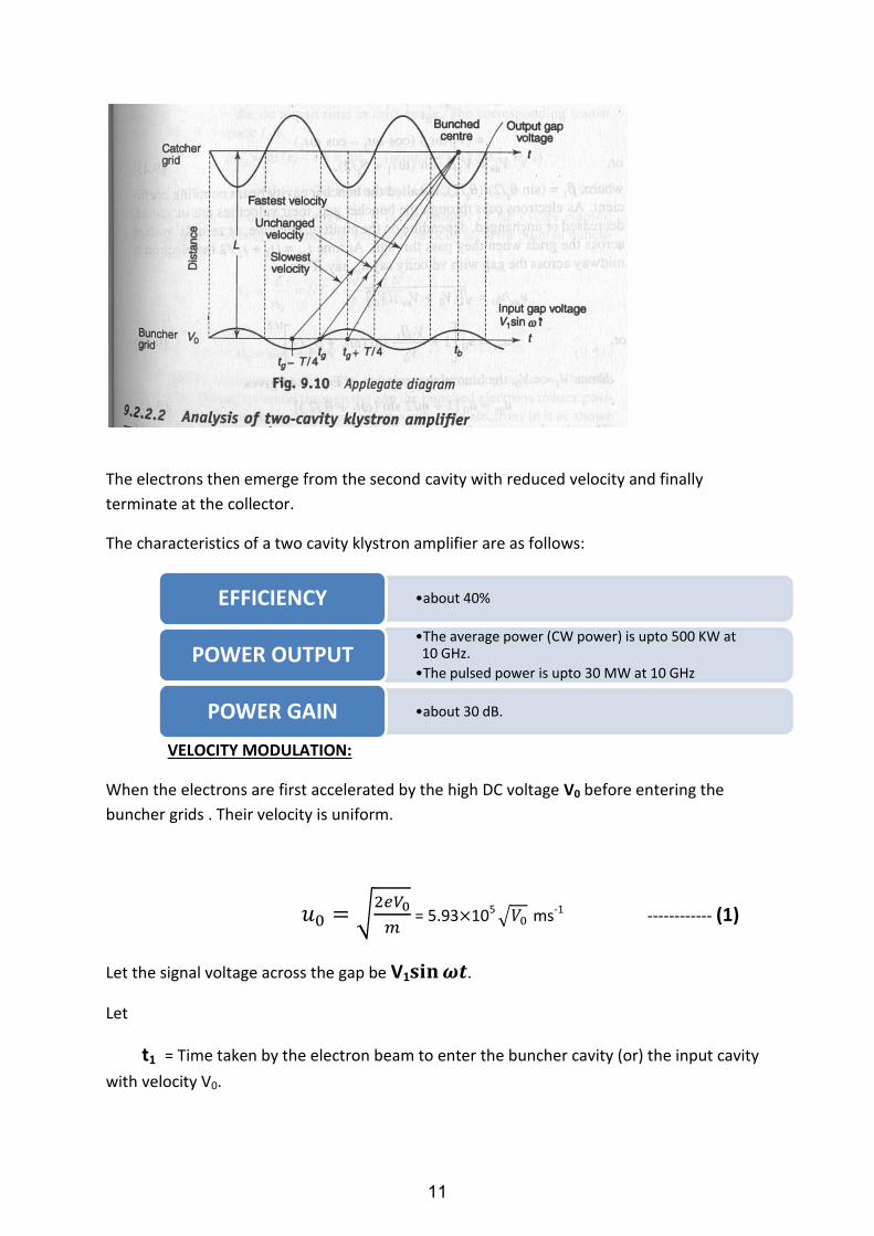
The electrons then emerge from the second cavity with reduced velocity and finally
terminate at the collector.
The characteristics of a two cavity klystron amplifier are as follows:
VELOCITY MODULATION:
When the electrons are first accelerated by the high DC voltage V0 before entering the
buncher grids . Their velocity is uniform.
√
= 5.93 105 √
ms-1 ------------ (1)
Let the signal voltage across the gap be V1 .
Let
t1 = Time taken by the electron beam to enter the buncher cavity (or) the input cavity
with velocity V0.
•about 40% EFFICIENCY
•The average power (CW power) is upto 500 KW at 10 GHz.
•The pulsed power is upto 30 MW at 10 GHz POWER OUTPUT
•about 30 dB. POWER GAIN
11
t2 = Time taken by the electron beam to pass out from the buncher cavity.
The transit time and transit angle through the transit gap is
----------- (2)
Transit angle,
----------- (3)
Due to input RF signal in the buncher cavity, the average RF voltage in the buncher gap can
be obtained as,
∫
*
+
---------- (4)
Let
A =
B =
Also, A+B =
A-B =
We know that,
=
=
[ ]
12

[ ]
Obtained by (A-B) Obtained by (A+B)
[ ]
We know that,
Equation (4) can be rewritten as,
[ (
)
]
(
)
(
) ------------------ (5)
where
= beam coupling co-efficient of buncher cavity gap
We know that, =
-
From (5), (
)
(
) ------------------ (6)
The exit velocity from buncher gap is given by,
√
-------------- (7)
=√ (
(
))
13

The factor
is known as depth of modulation.
If the modulation amplitude is very small (<<<1), then
(
(
)) -----------(8)
The factor
is represented as m.
(
(
)) -----------(9)
TRANSIT TIME IN DRIFT SPACE:
If t3 is the time when the bunched electrons are at the catcher grid after travelling through
the field free drift space.
-----------(10)
(
(
))
Let
be the transit time of the reference electron.
(
(
))
We know that,
(1+x)-1 = 1-x+x2-……………..
Neglecting the higher order terms we get,
(
(
)) ------------(11)
DENSITY MODULATION:
Because of the difference in velocities of electrons in the velocity modulated beam, the
electron will form bunches ie., becomes density modulated, in accordance with input cycle.
A maximum degree of bunching takes place when the buncher and catcher cavities are
spaced to satisfy the condition,
14

From (11),
(
(
)) -----------(12)
The corresponding transit angle in the drift space L is,
(From equation (12))
= (
(
))
=
(
) -----------(13)
where = = DC transit angle
The transit time of reference electron in terms of N is given by,
Where N = number of RF cycles that are elapsed during the transit time of reference
electron.
Now,
(
)
------------ (14)
Using equation (14), equation (11) can be rewritten as,
(
(
))
(
(
))
(
)
Let X be the bunching parameter and it is given by,
15

(
) -------------(15)
BUNCHED BEAM CURRENT: (ib)
The bunched beam current ib in the catcher cavity is given by,
(
)
( (
))
By Fourier expansion, the beam current of two cavity reflex klystron is,
∑
(
)
Expanding the summation we get,
(
)
∑
(
)
DC COMPONENT FUNDAMENTAL AC COMPONENT HARMONICS
The klystron is generally tuned to the fundamental AC component of current and it
is given by,
(
) -------------(16)
OPTIMUM DRIFT SPACE LENGTH: Lopt
-----------(17)
16
We know that,
-----------(18)
Substituting eqn.(18) in (17),we get
From the Bessel function table, is maximum ie., 0.582 at X=1.841
-----------(19)
POWER OUTPUT:
The fundamental component of RF beam current passing through the output cavity gap
induces a current in the catcher cavity.
Where → beam coupling coefficient of catcher cavity.
. [ ]
I2
I2
If the buncher and catcher cavities are identical, then
I2
The output equivalent circuit of two cavity reflex klystron is,
17
Rsho → Wall resistance of catcher cavity
Rb → Beam loading resistance
RL → External load resistance
Rsh → effective shunt resistance
The output power delivered to catcher cavity is,
[
]
EFFICIENCY:
The electronic efficiency of klystron amplifier is defined as the ratio of the output power to
the input power.
If the coupling co-efficient is perfect ie., and , then there is maximum
beam current in the catcher cavity.
The maximum electronic efficiency of two cavity reflex klystron is 58.2 %
18
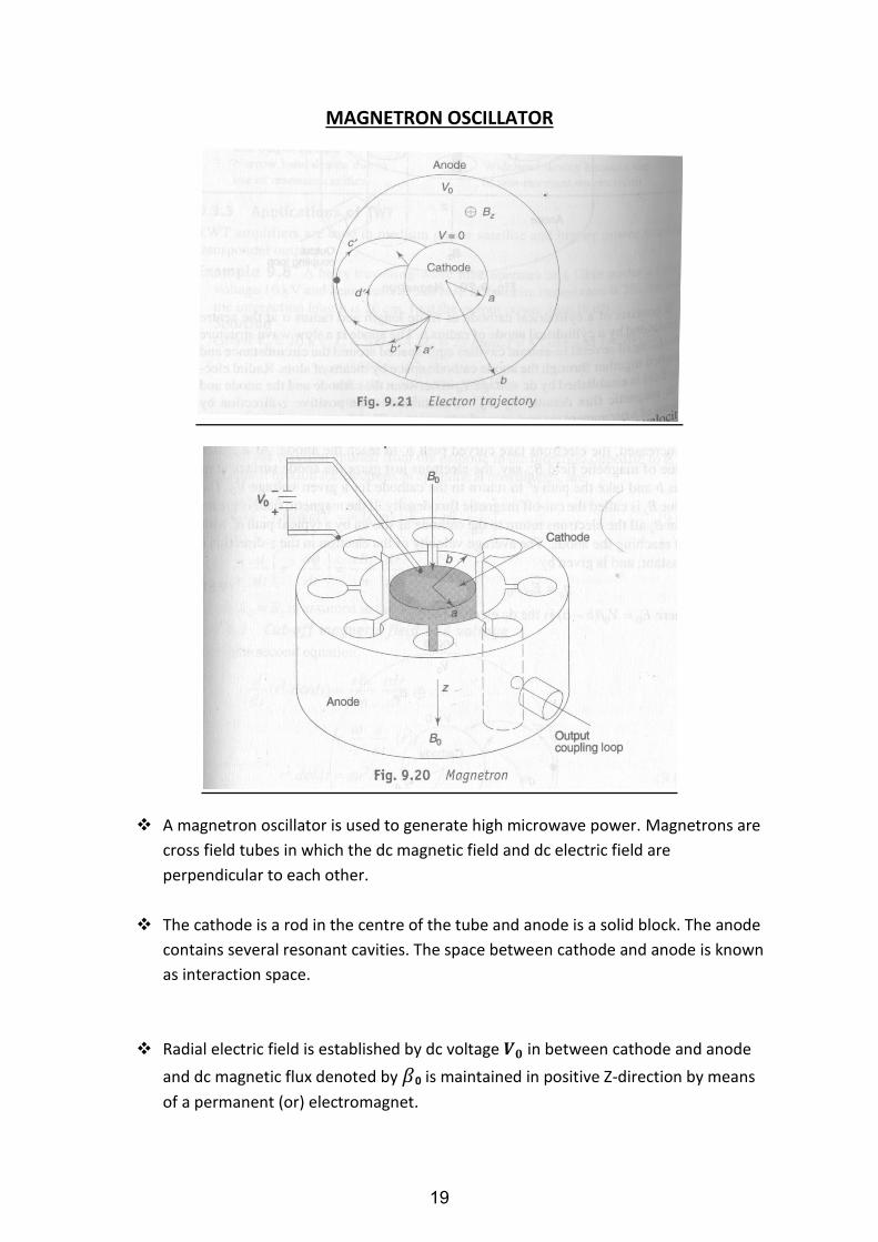
MAGNETRON OSCILLATOR
A magnetron oscillator is used to generate high microwave power. Magnetrons are
cross field tubes in which the dc magnetic field and dc electric field are
perpendicular to each other.
The cathode is a rod in the centre of the tube and anode is a solid block. The anode
contains several resonant cavities. The space between cathode and anode is known
as interaction space.
Radial electric field is established by dc voltage in between cathode and anode
and dc magnetic flux denoted by 0 is maintained in positive Z-direction by means
of a permanent (or) electromagnet.
19

There are three forces acting on an electron in the interaction region of the
magnetron,
force due to electric field (- eE)
force due to magnetic field [-e (V )]
centrifugal force (
)
The electrons emitted from the cathode try to travel towards anode.
At zero magnetic field, the electron takes the straight path a by the
influence of electric field only.
For a given , if the magnetic field is increased, the electrons take
curved path b to reach the anode.
At a critical value of magnetic field Bc , the electrons just graze the anode
surface and return to the cathode for a given voltage .The value B c is
called the cut-off magnetic flux density.
If the magnetic field is greater than Bc , all the electrons return to the
cathode by a typical path X without reaching the anode.
At the equilibrium condition,
------------- (1)
CENTRIFUGAL FORCE FORCE DUE TO FORCE DUE TO
ELECTRONS MAGNETIC FIELD
The electric field E is a function of radial direction only and is given by
(
) ------------ (2)
Where a and b are the anode and cathode radius respectively.
In the absence of electric field, the electrons move in a circular path and return to the
cathode, then
20
------------ (3)
Where is called the cyclotron angular frequency
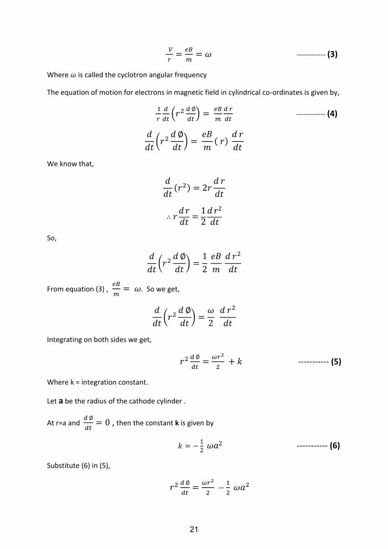
The equation of motion for electrons in magnetic field in cylindrical co-ordinates is given by,
(
)
------------ (4)
(
)
We know that,
So,
(
)
From equation (3) ,
. So we get,
(
)
Integrating on both sides we get,
----------- (5)
Where k = integration constant.
Let a be the radius of the cathode cylinder .
At r=a and
, then the constant k is given by
----------- (6)
Substitute (6) in (5),
21
(
)
(
) ------------ (7)
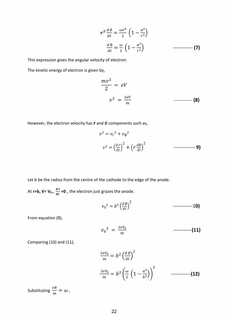
This expression gives the angular velocity of electron.
The kinetic energy of electron is given by,
------------- (8)
However, the electron velocity has r and components such as,
(
) (
) ------------- 9)
Let b be the radius from the centre of the cathode to the edge of the anode.
At r=b, V= V0 ,
=0 , the electron just grazes the anode.
(
) ------------10)
From equation (8),
-----------(11)
Comparing (10) and (11),
(
)
(
(
))
------------(12)
Substituting
,
22

*
(
)+
(
)
`
(
)
`
(
)
(
)
(
)
At the critical magnetic field, Bc = B
(
)
(
) ----------(13)
Thus if applied magnetic field B is greater than Bc for a given , the electron will not
reach the anode.
For a given B0, the cut off voltage is given by,
(
)
----------(14)
If V0< V c, for a given B, the electron will not reach the anode. Equations(3)and(14) for Bc
andVc called Hull- cut off magnetic and voltage equation, respectively.
RF STRUCTURE OF MAGNETRON:
Magnetron structure supports varieties of modes depending upon the phase
difference between fields in two adjacent cavities.
Boundary conditions are satisfied when total phase shift around the 8 cavities is a
multiple of 2π radians.
23

The phase shift between the fields of adjacent cavities is π radians. This is known as
π mode. Magnetron oscillators operated in π mode. * = π mode+
Frequency of π –mode can be easily separated from adjacent modes by
incorporating conducting straps connected to alternate segment of anode block.
If α is the mean separation between cavities , the phase constant of the fundamental
mode field is given by
Where
N=Total no of carriers
L=mean separation b/w cavities
N= integer indicating nth mode of oscillation
Oscillation mechanism
The electron beam a come across an electric field in the direction of its velocity . It is
retarded by the field, slow doen and drifts towards the anode valus of the static E and H
fields are so adjusted that the time he electron reaches near the second cavity. Last a time
period elapses ,The electron experiences a retarding field again and loses energy to the RF
field . This process continues the transfer of enegy takes place again near the third cavity.
Applications :
RADAR transmitters
Microwave owens
Industrial heating
TRAVELLING WAVE TUBE AMPLIFIER :
The travelling wave tube is broad band show wave devices . Its operation is based on he
interaction between the waves in the travelling wave structures and the electron beam.
TWT is an example of slow wave device. A slow wave device is a device in which an electron
beam is velocity modulated without a resonant cavity.
Operation of TWT :
Its operation is based on the interaction between the waves in the travelling wave structure
and the electron beam . It consists of
Two slow wave structure along the helix
The RF input near the cathode
A RF output near the collector
Focusing magnet
Electron beam
Cathode focusing plate
The structure is as shown below
24
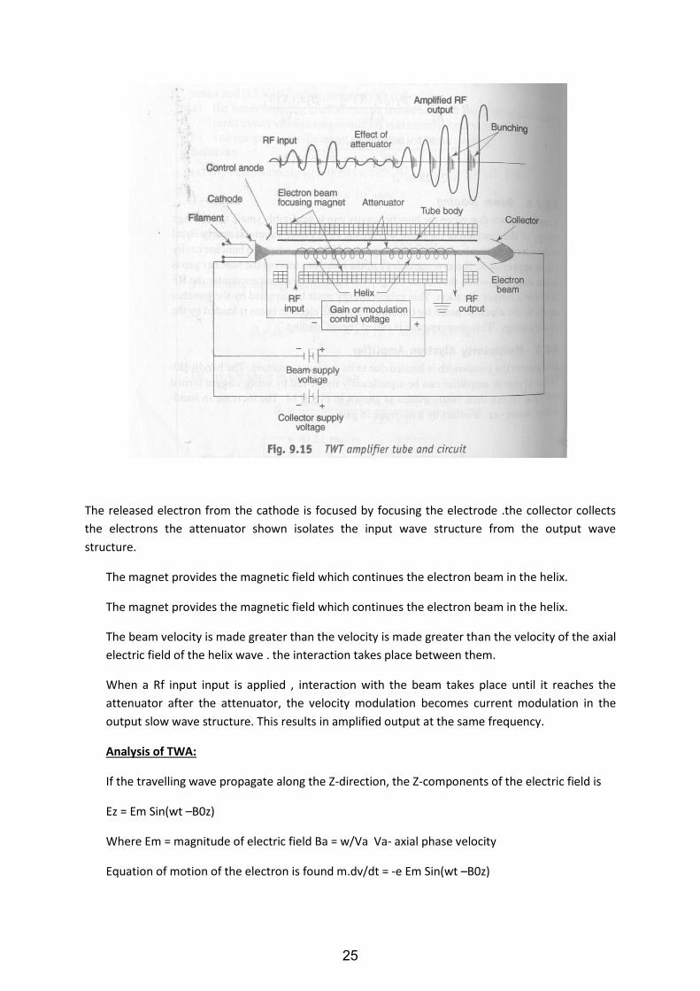
The released electron from the cathode is focused by focusing the electrode .the collector collects
the electrons the attenuator shown isolates the input wave structure from the output wave
structure.
The magnet provides the magnetic field which continues the electron beam in the helix.
The magnet provides the magnetic field which continues the electron beam in the helix.
The beam velocity is made greater than the velocity is made greater than the velocity of the axial
electric field of the helix wave . the interaction takes place between them.
When a Rf input input is applied , interaction with the beam takes place until it reaches the
attenuator after the attenuator, the velocity modulation becomes current modulation in the
output slow wave structure. This results in amplified output at the same frequency.
Analysis of TWA:
If the travelling wave propagate along the Z-direction, the Z-components of the electric field is
Ez = Em Sin(wt –B0z)
Where Em = magnitude of electric field Ba = w/Va Va- axial phase velocity
Equation of motion of the electron is found m.dv/dt = -e Em Sin(wt –B0z)
25
And the electron velocity is in the form of
V=Vdc + Ve cos(wet +oc)
V dc = dc electron velocity of the electron in the velocity modulated electron beam
Wc = angular frequency of velocity of electron
0c= phase angle
The magnitude of the velocity of the electron is found to be proportional to the magnitude of
the axial field . that is
Ve = e.Em/mWc
The conversion current in the electron beam induced by the axial electric field is given by i=
The above equation for I is called electronic equation
The equivalent circuit of slow wave is given by
The axial electrons field is given by
Em=(r2 .r0.z0.i)/( r2 -r0
2)
The above equation for Em is called circuit equation
The equation describes the effect of electron beam current on the axial electric field.
Gain parameter of TWT :
He gain parameter of TWT is defined as G=(Idc *Z0/4Vdc)^(1/3)
Output power gain Ap :
It is defined as
Ap=10log[v(l)/v(0)]^2
Here Lx is numerical number
l-circuit length
c-gain parameter
v(l)-the amplitude of output voltage
v(0)-voltage at Z=0
Microwave solid state devices
Microwave transistor
BJT
HBT hetero bipolar junction transistor
Tunnel diode
FET
JFET
26

MOSFET
HEMT
MESFET
NMOS,PMOS,CMOS
Memories
CCD
Transferred electron devices
Gunn diode
LSA diodes
INP
cdte
Avalanche transistor devices
Read diode
IMPATT diode
TRAPATT
BARITT
MESFET-metal oxide semiconductor field effect transistor
HEMT-High electron mobility transistors
CCD-charge coupled device
CdTe-candium telluride
LSH-Limited space charge accumulator diode
IMPATT- Impact conization avalanche transit time device
TRAPATT-Trapped plasma avalanche triggered transit time diode
BARITT-Barrier integrated transit time diodes
BJT MICROWAVE BIPOLAR TRANSISTOR :
The microwave transitor is a non-linardevice and its principle of operation is simmilar to that
of the low frequency device , but requirements for dimensions process control , heat sinking
and packaging are much more severe.
Feautures :
Bipolar transistor are used s amplifier and oscillators
They are used in L&S microwave band
They are operated as class C amplifiers
Their efficiency is about 50%
They are used to get a powergain of about 10db.
All silicon microwave transistors are of npn type as the mobility of the electrons is
higher than that of holes
27
In microwave transistors omitter stripwidth and base thickness are made very small.
In lithography the emitter strip width is a submission and this
Vertical cross sectional view of the microwave transistor :
Transistor fabbrication is carried out by a set of process known as planar technology.
A wafer n+ silicon is used as the substance .
A thin layer of n tye silicon is grown over this substance by epitaxial growth. This
consistutes n region for the collector.
P-base layer is formed by diffusion of p-type impurities (sio2 layer).
n-type sio-2 layer is diffused over the base layer to for n-emiter layer.
A final metalization process is used to make ohmic contacts to the emitter and the
base collector contacts is from the bottom of the n+ substance
Cut off frequency (ft) of the microwave transistor :
Ft=1/2*pi*t
Where t=transit time
.It is defined as the time taken by charge carriers to move from emitter to theto the
collector.This time of transitfrom emitter tocolllector is composed of four parts
1.Emitter charging time t0.
2.Collector space chase transit time esc
3.Collector charging time tc
Outout resistance Rout and input resistane Rin :
Rin- depends on theemmiter geometry and space between emitter and base contacts. It is inversely
proportional to the emiter periphery and it is directly proportional to emitter periphery and its
directly proportional to the distance between emitters and base contact.
Rout- depends on the output powe , class of the operation and operating voltage . To have large
outpu impedance , the base area must be minimized.
Aspect ratio = emiter area /base area
to obtain an optimum performance from a microwave transistor emitter periphery should be
minimized and the base area should be minimized.
Physical structure of microwave transistors :
28

Matrix Structure (Modified structure of overlay):
The maximum aspect ratio obtainable from these geomenmes depends upon the minimum width
that can be defined by photolithography for the purpose of diffusion .
The interdigitized type is for smalll signal and power , but the overlay type and matrix type for small
power only.
Microwave oscillator circuit design:
The following figure shows the realization of colpitts circuit at 2ghz
The base of the transistor is directly grounded to the ground to the ground plate of the stripline
board.
The capacitance c1 is provided by the phase loop with l2 and c2.
Unipolar Field-effect Transistors :
Field – effect transistors are manufactured from Ga As for higher frequency of opinion which is
achieved due to the higher electron mobility compared to Si. The most commonly used FET for
microwave frequencies is schottky barrier (MOS) gate and is called MESFET . In recent years a
hetero junction is formed at the interface of an aluminium- Ga As doped alloy and an un doped
GaAs layer which enables a channel with a very high electron mobility for higher frequency
operations and lower noise. The latter construction is called HEMT . MESFET devices can give a
single stage gain of 15db at noise figure less than 1db and HEMT devices give a gain of 15db at
8ghz with noise figure 0.4 db and 6db at 50ghz with noise figures of 1.8 db.
29
The basic construction and circuit symbol of the MESFET,HEMT are shown below.The basic
operations , equivalent circuit and biasing circuit of the MESFET are described here .the 3
terminals of the transistor are named source , gate and drain . the metal contacts of the
terminals of the schottky junction with the n-type semi conductor region called the channel for
charge carrier . The voltage on the gate controls the depletion region width and thus controls
the current from the source to the drain. The bandwidth of the device is given by
Ft = ½*pi*T
T-electron transit time through the channel. At microwave frequencies the channel length is
extremely short so that the MESFET can operate in 5-20 GHZ range .
The output drain current Id versus drain- to – source voltage Vds is shown below .for max
dynamic range the dc voltage of the gate must be negative with respect to the source. This is
schieved by grounding the gate through RF choke.
Microwave transistor amplifier design : at microwave frequencies transistor amplifier are
designed using S-parameters of the transistors and using input and output matching networks as
shown. Assuming that the transistor amplifier is unilateral and the transistor is conjugate
matched to the load and source, the maximum gain is given by
Gmax = Gi*Gt*G0.
Where Gi and G0 are determined by the input and output matching networks.
Microwave Transistor oscillator :
Microwave Transistor oscillators are designed by choosing the input and output port
terminations in the unstable regions where both the input and output impedances of the
transistor circuits will have a negative resistance.The oscillations will occur at a frequency at
which the total reactance in the input and output circuits becomes zero. Even if the transistor is
stable , it is made unstable by using feedback from the output to the input of the circuit. Any of
the standard low frequency oscillation circuits such as the Hartley , collpitts or clap circuits are
used in which the frequency stability is achieved by using a resonator in either the input or the
output circuits as part of the feedback loop.FET oscillator which is stabilized by using the
resonator in the input of the circuit.
Transversed electron devices (TED):
Gunn diod are negative resistance devices which are normally used as lowpower oscillator at
microwavve oscillation in gallium arsenide , indium phosphide and candium telluride.
Two vallley model of n-type ga As:
Transfer of electron densities :
1.when applied electric field is lower than the electric field of lower valley (E<El), no electrons will
penetrate to uppper valley
30
2.When the applied electric field is higher than that of the lower valley , than that of upper valley
(El<E<Eu), the electrons will begin to transfer upper valley.
3.when the applied electric field is higher than that of uppper valley (Eu <E) , all the electrons will
According to the energy band theory of n-type ga As , electron in the lower valley must havehigh
mobility , small effectiveness and lower valley must have high low mobility, large effectiveness and
high density state.
Since the conductivity is directly proportional to the mobility , the conductivityy and hence the
current decreases with an increase in E-field (or) voltages in an intermediate range , beyond a
threshhold value Vth . This is called transferred electron effect and the device is known as
transferred electron device over the range of applied negative resistance device device over a range
of applied negative device over a range of applied negative resistance device over the range of
applkied negative voltage and can be used in microwave oscillators voltages and can be used in
microwave oscillators voltages and can be used in microwave oscillators.
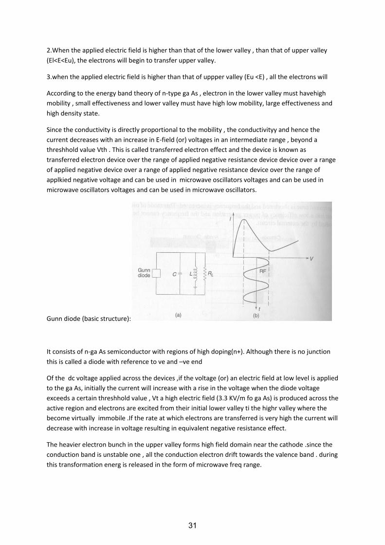
Gunn diode (basic structure):
It consists of n-ga As semiconductor with regions of high doping(n+). Although there is no junction
this is called a diode with reference to ve and –ve end
Of the dc voltage applied across the devices ,if the voltage (or) an electric field at low level is applied
to the ga As, initially the current will increase with a rise in the voltage when the diode voltage
exceeds a certain threshhold value , Vt a high electric field (3.3 KV/m fo ga As) is produced across the
active region and electrons are excited from their initial lower valley ti the highr valley where the
become virtually immobile .If the rate at which electrons are transferred is very high the current will
decrease with increase in voltage resulting in equivalent negative resistance effect.
The heavier electron bunch in the upper valley forms high field domain near the cathode .since the
conduction band is unstable one , all the conduction electron drift towards the valence band . during
this transformation energ is released in the form of microwave freq range.
31

The current in the high field domain is decrased andit is moved towards the anode again high field
domain is formed near the cathode and the process is continued to get oscilation.
Gunn diode oscillator circuit:
The diode is mounted at one end of the cavity and is in continuation with the central conductor of
the coaxial line
The frequency of oscillation is determined by the length of the cavity and location of the coupling
loop within the resonator determine s the load impedance presented in the diode
Heat sink is included to conduct away the hat generated by the power dissipated in the devices.
Avalanche transit time device :
32

IMPATT diode means impact ionization avalanche transit time diode, It’s operation depends on the
reverse breakdown voltage characteristics of p-n junction and phase dlay of the applied RF signal.
Mechanism of oscillation:
The diode resonator circuit noise voltage excites resonant component. The reverse biased dc
field and ac field makes the diode to swing in to and out of the avalanche condition .The
carrier drift to the end contacts before the diode swings out of the avalanche region. This
happens as the drift time is very short . As a result , the arc field takes energy from the
carriers dc bias source .This process builds the microwave oscillation in the circuit.
The frequency of oscillation is given by
F=Vd/2l
Vd = drift velocity of the holes
L = length of the drift region
IMPATT diode:
ANALYSIS OF IMPATT DIODE :
The transit angle is given by
Where t= transit time
The avalanche resonant frequency is given by
A=diode cross section
I= current
In terms of transit time, the frequency of the diode is given by
33

VI characteristics of IMPATT diode :
Efficiency of IMPATT diode
Salient features
It is an avalanche transit time device
It can be made with germanium , silicon and gallium arsenide
It is useful up to 100ghz
It provides higher continuous power compared to other semiconductor devices
It’s efficiency is less than 30%
It is useful at microwave, millimeter an sub millimeter wave frequencies
It is used in digital, analogue communications and radar systems.
It can be used as an amplifier or oscillator
The reactance of the circuit is made zero by controlling the conductance
Rnd = -ve resistance, Cj = junction capacitance
Lp = package lead conductance, Cp = capacitance bw package terminals
34
APPLICATION OF IMPATT diode:
As microwave oscillator
As modulated oscillator
As receiver local oscillator
As parametric amplifier pump
In radar reception
In communication transmission
As - ve resistance
ADVANTAGES:
It is wideband
Pulse power is high
Suitable for high frequency
DISADVANTAGES:
It is a noisy device
Tuning range is not high
TRAPPAT diode:
Principle of operation:
It is operated in the reverse bias. During the application of high reverse
voltage, phenomenon takes. The depletion layer is filled with a plasma of
electrons and holes. These are trapped in low field region behind propagating
high field. A voltage pulse is produced and it apposes the applied dc voltage.
The decreased voltage reduces the current pulse. The decreased current with
increased voltage creates a negative resistance region. Basically, TRAPPAT
oscillators depend on the delay in the current caused by the delay in the current
caused by the avalanche process.
the frequency of oscillation of a TRAPPAT diode is, f=1/2T
T=2[w/vf + w/2(1/vp = 1/vs)
W=Depletion layer width
Vf =front velocity
Vp=plasma velocity
35

Vs=saturated velocity
SALIENT FEATURES:
Its structure has p+ n n+ (or) n+ p p+.
It is a high efficiency diode oscillator.
Its oscillations depend on the delay in the current caused by the
avalanche process.
The diode diameter is about 50µm for cw operation and it 750µm at
lower frequency for high peak power application.
It can be operated over a range of 400MHZ to 12MHZ.
It has an efficiency of 20-40%.
ANALYSIS:
The transit time of charge carriers is given by <t=l/vs.
l-drift region length.
Vs-drift velocity.
Voltage waveform of TRAPATT diode:
The avalanche zone velocity,vaz is given by vaz=J/Ena.
j-current density,A/m2.
e-electron charge=1.6*10-19c.
Application of TRAPATT DIODE:
It is used in lower power Doppler radars.
As local oscillators in different radar phased array radars etc.
I. In ratio altimetors.
In microwave beacons and landing systems.
36

Advantages:
Its efficiency is relatively high.
It can be used over a frequency range of few hundred MHZ to several
MHZ.
Disadvantages:
It has high noise figure.
Its use at upper microwave frequencies is limited.
It generates strong harmonics due to short duration current pulse.
BARITT DIODE:
Barrier injected transit time diode.
It is low noise microwave oscillator, but it is used as amplifier rather than
oscillator.
Salient features:
low noise µw oscillator.
It can be used up to x-band µw frequencies.
Narrow band, low efficiency device.
Its output power is less than 1mw.
It is used as amplifier rather than oscillator.
Parametric amplifiers:
Parametric device: a parametric device is one that uses a non-linear
reactance(capacitance or conductance) or time varying reactance.
Parametric amplifiers:
A parametric amplifier is named because of its operation due to periodic
variation of the device parameters such as capacitance of the varactor diode
unfer the influence of a suitable pump signal.
If a small input signal as a frequency fs and the ac power source operated as
pumping signal at a frequency fp , are applied together to the varactor diode,
37

linear amplification of a small signal results in due to time varying capacitance
of the diode.
Manley-rowe relations:
This relations are useful in determining the maximum gain of the
parametric amplifier.
Fig: equivalent ckt of manley rowe relations
Manley rowe relations is given by
∑ ∑
nm/nfs+mfp =0=∑ ∑
mn/nfs+mfp.
Where pnm-avg power at the output frequencies |nfs + mfp |.
Analysis of parametric amplifier:
In superheterodyne receiver a radio frequency signal may be mixed with a
signal from the local oscillator in a non-linear circuit(the mixer) to generate
sum and difference frequencies. In a parametric amplifier the local oscillator is
replaced by a pumping generator such as a reflex klystron and non linear
element by time varying capacitor such as varactor diode.
38
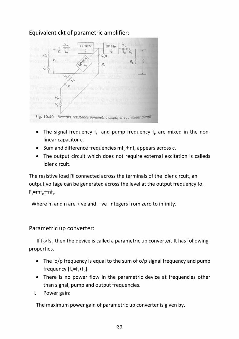
Equivalent ckt of parametric amplifier:
The signal frequency fs and pump frequency fp are mixed in the non-
linear capacitor c.
Sum and difference frequencies mfp nfs appears across c.
The output circuit which does not require external excitation is calleds
idler circuit.
The resistive load Rl connected across the terminals of the idler circuit, an
output voltage can be generated across the level at the output frequency fo.
Fs=mfp nfs.
Where m and n are + ve and –ve integers from zero to infinity.
Parametric up converter:
If fo>fs , then the device is called a parametric up converter. It has following
properties.
The o/p frequency is equal to the sum of o/p signal frequency and pump
frequency [fo=fs+fp].
There is no power flow in the parametric device at frequencies other
than signal, pump and output frequencies.
I. Power gain:
The maximum power gain of parametric up converter is given by,
39
Gain = fo/fs * x/(1+√ )2.
Where fo=fs+fp.
X=fs/fo*(∂Q)^2.
∂Q=figure of merit of non linear capacitor.
∂=factor of merit figure.
Q=1/2∏ fscrd.
Rd=series resistance of pn-junction diode.
II. Noise figure:
One advantage of parametric amplifier over the transistor amplifier is its
low noise figure, because a pure reactance does not contribute thermal
noise to the circuit. F of parametric up converter is given by,
F=1+ 2Td/To *1 /∂Q +1 /(∂Q)2].
Where Td= diode temperature in degrees Kelvin.
To= 3000k is the ambient temperature in degrees Kelvin.
∂Q=figure of merit for the non-linear capacitor.
III. Band width:
It is given by,
Bw = 2∂√ .
Parametric down converter:
If fo<<fs, then the device is called a parametric down converter. The
output frequency is equal to the difference between the signal
frequency and pump frequency [fo=fs-fp].
Here its power gain is actually a loss.
The down conversion gain is given by,
Gain = = fs/fo * x/(1+√ )2.
40
Negative resistanace parametric amplifier:
In parametric amplifier, capacitor delivers power to the signal generator at fs
instead of absorbing it. Due to that, the power gain may be infinite, which is an
unstable condition and the circuit may be oscillating both fs and fo. this is
another type of parametric device , often called as a negative resistance
parametric amplifier.
i. Power gain:
The output power is taken from the resistance Ri at a frequency
fiand the conversion gain from fs to fi.
Gain = 4fi/fs . Rg Ri/RTs.RTi . a/(1-a)2.
Fs-signal frequency ; fp-pump frequency.
Fi=fp-fs=idles frequency.
Rg- output resistance of signal generator.
Ri- output resistance of idles generator.
RTs- total resistance at fs.
RTi- total resistance at fi; a=R/RTs ; R = ∂2/ s ic2RTi.
ii. Noise figure:
F = 1 + 2Td/To *1/∂Q + 1/(∂Q)2].
iii. Band width:
Bw = ∂/2 √ i/fs ; fi=4fs.
Bw = ∂ = 0.3.
Problem:
A up-converter parametric amplifier has the following
parameters.
Ratio of o/p freq. over sign freq fo/fs = 25.
Figure of merit ∂Q = 10.
Factor of merit figure ∂ = 0.4.
Diode temperature Td = 350k.
Calculate a)power gain in decibels b) the noise figure in decibels c)
the band width.
a)Power gain = 9.55 ->9.80dB
b)f->1.26->1dB
c)4.
41