microprocessor programming and system …edutechlearners.com/download/mp/microprocessor...
TRANSCRIPT

MICROPROCESSOR PROGRAMMING
AND SYSTEM DESIGN

2
ROAD MAPSDK-86
Intel 8086 Features
8086 Block Diagram
8086 Architecture
Bus Interface Unit
Execution Unit
8086 Architecture
8086 Programmer’s Model
Flag Register
Memory Segmentation

Intel 8086 Programming and System
Design
What the course is about? Introduction to Programmers Model of Intel 8086
Instruction set and Assembly Language Programming
Pin out Diagram and Functions of Various Pins
Connecting the memory to Microprocessor: Bus Cycle
and Timing Diagrams
Data Transfer Schemes
Interrupts
Interfacing I/O Devices
3

SDK-86 The SDK-86 single board computer originally was a kit. Intel sold the
rights to it to URDA, and it is still available as an assembled board.
<-- Serial port
<-- 7 segment displays
<--- Keypad
4
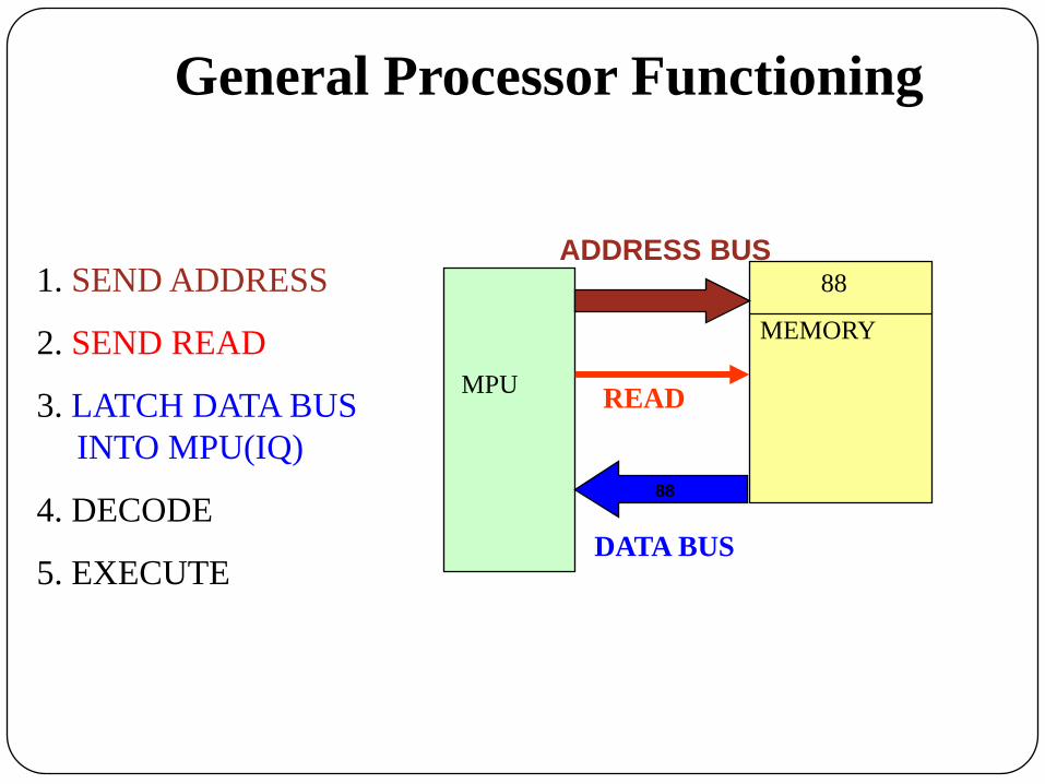
MPU
MEMORY
DATA BUS
READ
ADDRESS BUS1. SEND ADDRESS
2. SEND READ
3. LATCH DATA BUS
INTO MPU(IQ)
4. DECODE
5. EXECUTE
88
88
General Processor Functioning
Intel 8086 Features
16-bit Arithmetic Logic Unit.
16-bit data bus (8088 has 8-bit data bus)
20-bit address bus - 220 = 1,048,576 = 1 Mb
The address refers to a byte in memory. In the 8088,these bytes come in on the 8-bit data bus. In the 8086,bytes at even addresses come in on the low half of thedata bus (bits 0-7) and bytes at odd addresses come inon the upper half of the data bus (bits 8-15).
6
Intel 8086 Features ( Contd.)
The 8086 can read a 16-bit word at an evenaddress in one operation and at an odd address intwo operations. The 8088 needs two operations ineither case.
The least significant byte of a word on an 8086family microprocessor is at the lower address.
7

Intel 8086 Features ( Contd.)
It can support up to 64K I/O ports.
It provides 14, 16 -bit registers.
It has multiplexed address and data bus AD0- AD15 and
A16 – A19.
It requires single phase clock with 33% duty cycle to provide
internal timing.
8

Intel 8086 Features ( Contd.)
8086 is designed to operate in two modes, Minimum and
Maximum.
It can prefetches up to 6 instruction bytes from memory
and queues them in order to speed up instruction
execution.
It requires +5V power supply.
A 40 pin dual in line package
9

8086 Block Diagram
10

8086 Architecture
The 8086 has two parts, the Bus Interface Unit(BIU) and the Execution Unit (EU).
The BIU fetches instructions, reads and writesdata, and computes the 20-bit address.
The EU decodes and executes the instructionsusing the 16-bit ALU.
11

8086 Architecture ( Contd.)
The BIU contains the following registers:
IP - the Instruction Pointer
CS - the Code Segment Register
DS - the Data Segment Register
SS - the Stack Segment Register
ES - the Extra Segment Register
The BIU fetches instructions using the CS and IP, writtenCS:IP, to construct the 20-bit address. Data is fetched using asegment register (usually the DS) and an effective address(EA) computed by the EU depending on the addressing mode.
12

Bus Interface Unit
BUS INTERFACR UNIT:
It provides a full 16 bit bidirectional data bus and 20 bit
address bus.
The bus interface unit is responsible for performing all
external bus operations.
Specifically it has the following functions:
Instruction fetch, Instruction queuing, Operand fetch and
storage, Address relocation and Bus control.
13
Bus Interface Unit ( Contd.)
The BIU uses a mechanism known as an instruction stream
queue to implement a pipeline architecture.
This queue permits prefetch of up to six bytes of instruction
code. When ever the queue of the BIU is not full, it has room
for at least two more bytes and at the same time the EU is
not requesting it to read or write operands from memory,
the BIU is free to look ahead in the program by prefetching
the next sequential instruction.
14

Bus Interface Unit ( Contd.)
These prefetching instructions are held in its FIFO queue. With its
16 bit data bus, the BIU fetches two instruction bytes in a single
memory cycle.
After a byte is loaded at the input end of the queue, it automatically
shifts up through the FIFO to the empty location nearest the
output.
The EU accesses the queue from the output end. It reads one
instruction byte after the other from the output of the queue. If the
queue is full and the EU is not requesting access to operand in
memory.
These intervals of no bus activity, which may occur between bus
cycles are known as Idle state.15

Bus Interface Unit ( Contd.)
If the BIU is already in the process of fetching an instruction
when the EU request it to read or write operands from
memory or I/O, the BIU first completes the instruction fetch
bus cycle before initiating the operand read / write cycle.
The BIU also contains a dedicated adder which is used to
generate the 20bit physical address that is output on the
address bus. This address is formed by adding an appended 16
bit segment address and a 16 bit offset address.
16
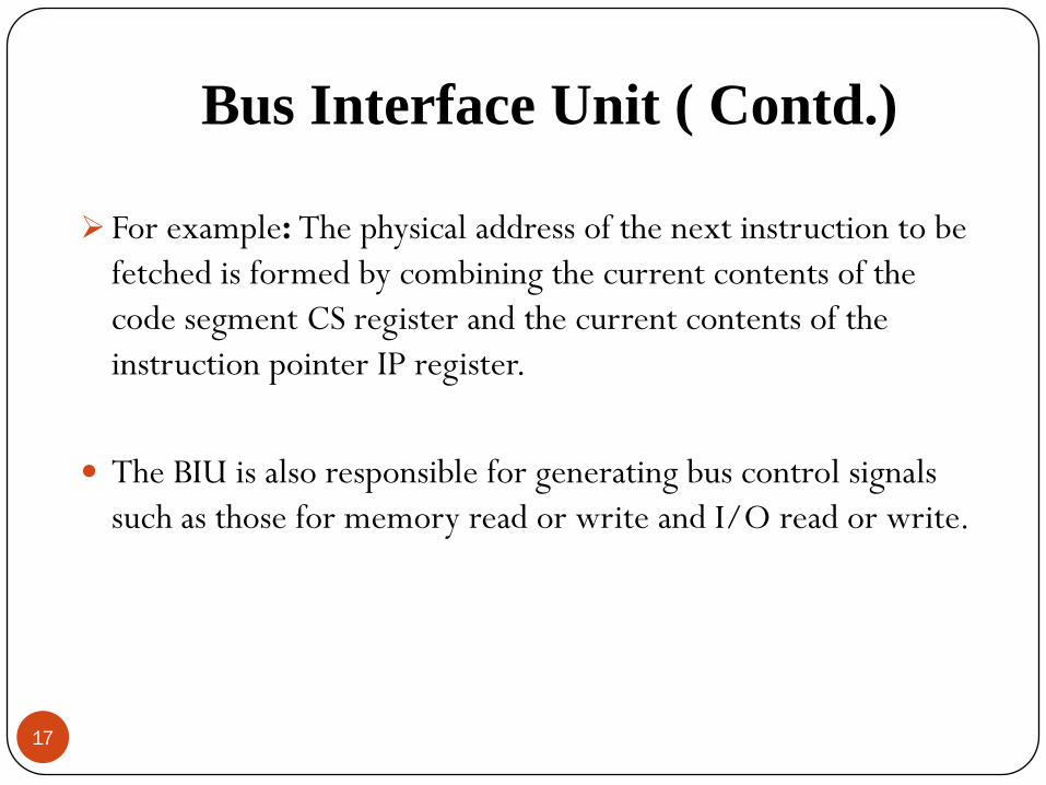
Bus Interface Unit ( Contd.)
For example: The physical address of the next instruction to be
fetched is formed by combining the current contents of the
code segment CS register and the current contents of the
instruction pointer IP register.
The BIU is also responsible for generating bus control signals
such as those for memory read or write and I/O read or write.
17
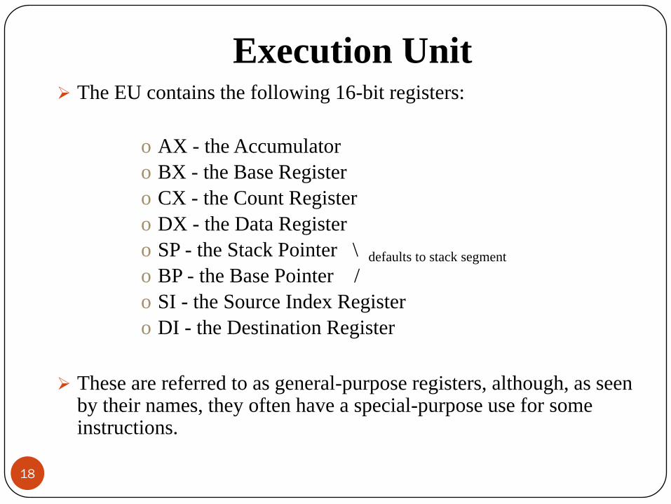
Execution Unit The EU contains the following 16-bit registers:
o AX - the Accumulator
o BX - the Base Register
o CX - the Count Register
o DX - the Data Register
o SP - the Stack Pointer \ defaults to stack segment
o BP - the Base Pointer /
o SI - the Source Index Register
o DI - the Destination Register
These are referred to as general-purpose registers, although, as seenby their names, they often have a special-purpose use for someinstructions.
18
Execution Unit
The Execution unit is responsible for decoding and executing all
instructions.
The EU extracts instructions from the top of the queue in the
BIU, decodes them, generates operands if necessary, passes them
to the BIU and requests it to perform the read or write bys
cycles to memory or I/O and perform the operation specified by
the instruction on the operands.
During the execution of the instruction, the EU tests the status
and control flags and updates them based on the results of
executing the instruction.19

Execution Unit ( Contd.)
If the queue is empty, the EU waits for the next instruction byte
to be fetched and shifted to top of the queue.
When the EU executes a branch or jump instruction, it transfers
control to a location corresponding to another set of sequential
instructions.
Whenever this happens, the BIU automatically resets the queue
and then begins to fetch instructions from this new location to
refill the queue.
20

8086 Architecture
The AX, BX, CX, and DX registers can be considers as two 8-bitregisters, a High byte and a Low byte. This allows byte operationsand compatibility with the previous generation of 8-bit processors,the 8080 and 8085. 8085 source code could be translated in 8086code and assembled.
The 8-bit registers are:
o AX --> AH,AL
o BX --> BH,BL
o CX --> CH,CL
o DX --> DH,DL
21

8086 Programmer’s Model
ES
CS
SS
DS
IP
AH
BH
CH
DH
AL
BL
CL
DL
SP
BP
SI
DI
FLAGS
AX
BX
CX
DX
Extra Segment
Code Segment
Stack Segment
Data Segment
Instruction Pointer
Accumulator
Base Register
Count Register
Data Register
Stack Pointer
Base Pointer
Source Index Register
BIU registers(20 bit adder)
EU registers16 bit arithmetic
22

General Purpose Registers
8086 CPU has 8 general purpose registers, each
register has its own name :
AX - the accumulator register (divided into AH / AL).
BX - the base address register (divided into BH / BL). CX
- the count register (divided into CH / CL).
DX - the data register (divided into DH / DL).
SI - source index register.
DI - destination index register. (vii) BP - base pointer.
SP - stack pointer.
23
Segment Register
CS - points at the segment containing the current program.
DS - generally points at segment where variables are
defined.
ES - extra segment register, it’s up to a coder to define its
usage.
SS - points at the segment containing the stack.
24

Special Purpose Registers
IP - the instruction pointer.
Flags Register - deter mines the current state of the
processor.
IP register always works together with CS segment register
and it points to currently executing instruction.
Flags Register is modified automatically by CPU after
mathematical operations, this allows to determine the type of
the result, and to determine conditions to transfer control to
other parts of the program. Generally you cannot access
these registers directly.
25

Overflow Flag
Direction Flag
Interrupt Flag
Trap Flag Sign Flag Zero Flag
Auxiliary Carry Flag
Parity Flag
Carry Flag

Flag Register ( Contd.)
Carry Flag (CF) - set if there was a carry from or borrow
to the most significant bit during last result calculation.
Parity Flag (PF) - set if parity (the number of “1” bits) in
the low-order byte of the result is even.
Auxiliary carry Flag (AF) - set if there was a carry from
or borrow to bits 0-3 in the AL register.
Zero Flag (ZF) - set if the result is zero.
Sign Flag (SF) - set if the most significant bit of the result is
set.
27
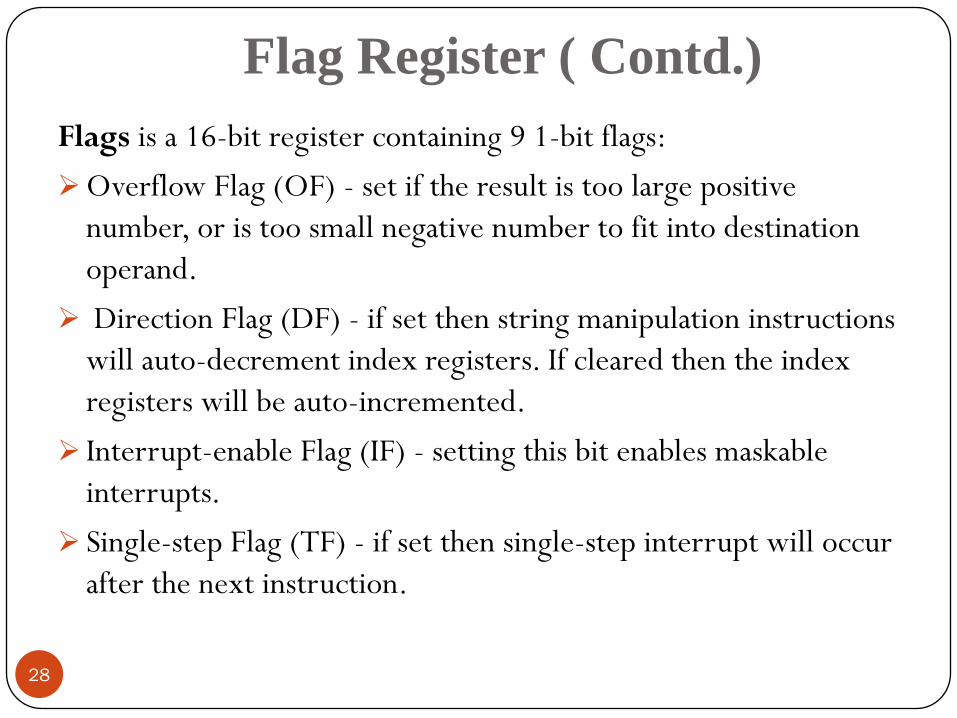
Flag Register ( Contd.)
Flags is a 16-bit register containing 9 1-bit flags:
Overflow Flag (OF) - set if the result is too large positive
number, or is too small negative number to fit into destination
operand.
Direction Flag (DF) - if set then string manipulation instructions
will auto-decrement index registers. If cleared then the index
registers will be auto-incremented.
Interrupt-enable Flag (IF) - setting this bit enables maskable
interrupts.
Single-step Flag (TF) - if set then single-step interrupt will occur
after the next instruction.
28

Memory Segmentation
SegmentRegisters
CODE
STACK
DATA
EXTRA
MEMORY
Address0H
0FFFFFH
64K CodeSegment
64K DataSegment
Segments are < or = 64K,can overlap, start at an addressthat ends in 0H.
CS:0
Segment Starting address is segmentregister value shifted 4 places to the left.
29

8086 Memory Terminology
CODE
DATA
STACK
EXTRA
0100H
0B200H
0CF00H
0FF00H
DS:
SS:
ES:
CS:
01000H
0B2000H
0CF000H
0FF000H
10FFFH
0C1FFFH
0DEFFFH
0FFFFFH
0HSegment Registers
Memory Segments
Segments are < or = 64K and can overlap.
Note that the Code segment is < 64K since 0FFFFFH is the highest address.
30

Code Segment
MemorySegment Register
Offset
Physical orAbsolute Address
0
+
CS:
IP
0400H
0056H
4000H
4056H
0400
0056
04056 H
The offset is the distance in bytes from the start of the segment.The offset is given by the IP for the Code Segment.Instructions are always fetched with using the CS register.
The physical address is also called the absolute address.
CS:IP = 400:56Logical Address
0H
0FFFFFH
31

The Stack Segment
Memory
Segment Register
Offset
Physical Address
+
SS:
SP
0A00
0100
0A000H
0A100H
0A00 0
0100
0A100H
The stack is always referenced with respect to the stack segment register.The stack grows toward decreasing memory locations.The SP points to the last or top item on the stack.
PUSH - pre-decrement the SPPOP - post-increment the SP
The offset is given by the SP register.
SS:SP
0FFFFFH
32

The Data Segment
Memory
Segment Register
Offset
Physical Address
+
DS:
EA
05C0
0050
05C00H
05C50H
05C0 0
0050
05C50H
DS:EA
0H
0FFFFFH
33
Data is usually fetched with respect to the DS register.
The effective address (EA) is the offset.
The EA depends on the addressing mode.
