micron dram products overview - nxp semiconductors · dll/odt no/no no/no no/yes yes/yes yes/yes...
TRANSCRIPT
©2012 Micron Technology, Inc. All rights reserved. Products are warranted only to meet Micron’s production data sheet specifications. Information, products, and/or specifications are subject to change without notice. All information is provided on an “AS IS” basis without warranties of any kind. Dates are estimates only. Drawings are not to scale. Micron and the Micron logo are trademarks of Micron Technology, Inc. All other trademarks are the property of their respective owners.
1 ©2012 Micron Technology, Inc. |
August 2013
John Quigley – Micron FAE
Micron DRAM Products Overview
August 27, 2013
2 ©2012 Micron Technology, Inc. | August 27, 2013
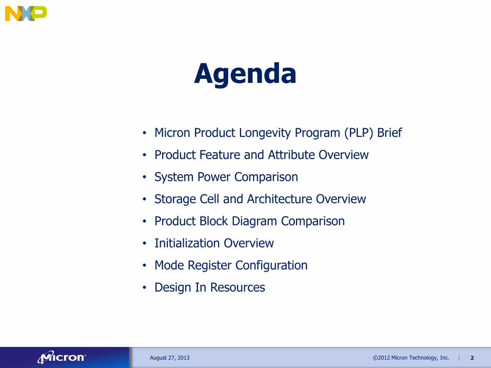
Agenda
• Micron Product Longevity Program (PLP) Brief
• Product Feature and Attribute Overview
• System Power Comparison
• Storage Cell and Architecture Overview
• Product Block Diagram Comparison
• Initialization Overview
• Mode Register Configuration
• Design In Resources
3 ©2012 Micron Technology, Inc. | August 27, 2013
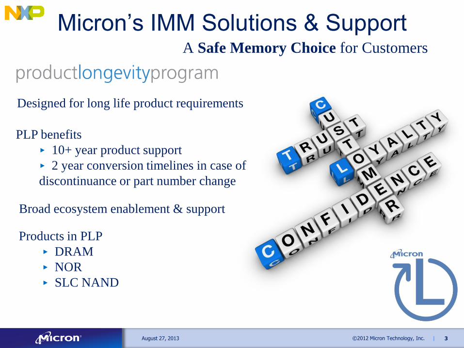
A Safe Memory Choice for Customers
Designed for long life product requirements
Products in PLP
▶ DRAM
▶ NOR
▶ SLC NAND
Broad ecosystem enablement & support
PLP benefits
▶ 10+ year product support
▶ 2 year conversion timelines in case of
discontinuance or part number change
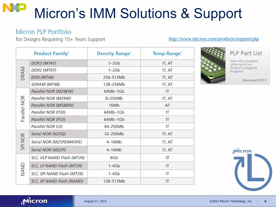
Micron’s IMM Solutions & Support
4 ©2012 Micron Technology, Inc. | August 27, 2013
Micron’s IMM Solutions & Support
http://www.micron.com/products/support/plp
5 ©2012 Micron Technology, Inc. | August 27, 2013
DRAM Product Feature and Attribute
Overview
(for AIMM Market)
6 ©2012 Micron Technology, Inc. | August 27, 2013
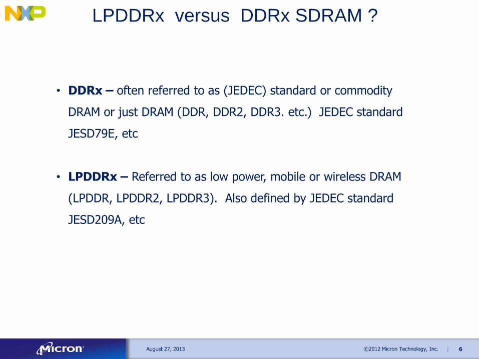
LPDDRx versus DDRx SDRAM ?
• DDRx – often referred to as (JEDEC) standard or commodity
DRAM or just DRAM (DDR, DDR2, DDR3. etc.) JEDEC standard
JESD79E, etc
• LPDDRx – Referred to as low power, mobile or wireless DRAM
(LPDDR, LPDDR2, LPDDR3). Also defined by JEDEC standard
JESD209A, etc
7 ©2012 Micron Technology, Inc. | August 27, 2013
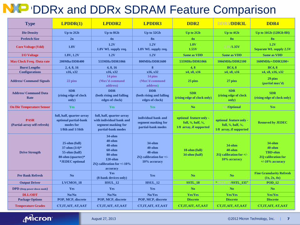
Type LPDDR(1) LPDDR2 LPDDR3 DDR2 DDR3/DDR3L DDR4
Die Density Up to 2Gb Up to 8Gb Up to 32Gb Up to 2Gb Up to 4Gb Up to 16Gb (128Gb 8H)
Prefetch Size 2n 4n 8n 4n 8n 8n
Core Voltage (Vdd) 1.8V 1.2V
1.8V WL supply req.
1.2V
1.8V WL supply req.
1.8V
1.55V 1.5V/1.35V
1.2V
Separate WL supply 2.5V
I/O Voltage 1.8V, 1.2V 1.2V 1.2V Same as VDD Same as VDD Same as VDD
Max Clock Freq. /Data rate 200Mhz/DDR400 533MHz/DDR1066 800MHz/DDR1600 533MHz/DDR1066 1066MHz/DDR2100 1600MHz+/DDR3200+
Burst Lengths 2, 4, 8, 16 4, 8, 16 8 4, 8 BC4, 8 BC4, 8
Configurations x16, x32 x16, x32 x16, x32 x4, x8, x16 x4, x8, x16 x4, x8, x16, x32
Address/ Command Signals 22 pins
14 pins
(Mux’d command
address)
14 pins
(Mux’d command
address)
25 pins 27 pins 29 pins
(partial mux’d)
Address/ Command Data
Rate
SDR
(rising edge of clock
only)
DDR
(both rising and falling
edges of clock)
DDR
(both rising and falling
edges of clock)
SDR
(rising edge of clock only)
SDR
(rising edge of clock
only)
SDR
(rising edge of clock only)
On Die Temperature Sensor Yes Yes Yes No No/Optional Yes
PASR
(Partial-array self refresh)
full, half, quarter-array
optional partial-bank
modes for
1/8th and 1/16th
full, half, quarter-array
with individual bank and
segment masking for
partial-bank modes
individual bank and
segment masking for
partial-bank modes
optional feature only -
full, ¾, half, ¼,
1/8 array, if supported
optional feature only -
full, ¾, half, ¼,
1/8 array, if supported
Removed by JEDEC
Drive Strength
25-ohm (full)
37-ohm (3/4)*
55-ohm (half)
80-ohm (quarter)*
*JEDEC optional
34-ohm
40-ohm
48-ohm
60-ohm
80-ohm
120-ohm
ZQ calibration for +/-10%
accuracy
34-ohm
40-ohm
48-ohm
ZQ calibration for +/-
10% accuracy
18-ohm (full)
34-ohm (half)
34-ohm
40-ohm
ZQ calibration for +/-
10% accuracy
34-ohm
40-ohm
TBD-ohm
ZQ calibration for
+/-10% accuracy
Per Bank Refresh No Yes
(8-bank devices only) Yes No No
Fine Granularity Refresh
(1x, 2x, 4x)
Output Driver LVCMOS_18 HSUL_12 HSUL_12 SSTL_18 “SSTL_15/SSTL_135” POD_12
DPD (Deep power-down mode) Yes Yes Yes No No No
DLL/ODT No/No No/No No/Yes Yes/Yes Yes/Yes Yes/Yes
Package Options POP, MCP, discrete POP, MCP, discrete POP, MCP, discrete Discrete Discrete Discrete
Temperature Grades CT,IT,AIT, AT,AAT CT,IT,AIT, AT,AAT CT,IT,AIT, AT,AAT CT,IT,AIT, AT,AAT CT,IT,AIT, AT,AAT CT,IT,AIT, AT,AAT
LPDDRx and DDRx SDRAM Feature Comparison
8 ©2012 Micron Technology, Inc. | August 27, 2013
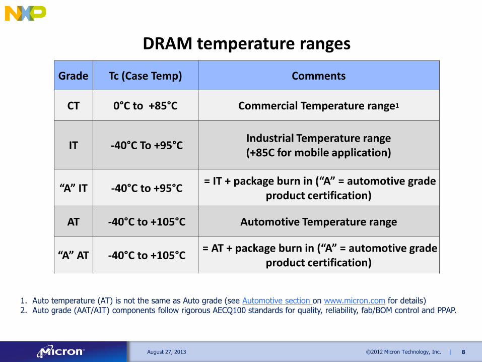
DRAM temperature ranges
Grade Tc (Case Temp) Comments
CT 0°C to +85°C Commercial Temperature range1
IT -40°C To +95°C Industrial Temperature range (+85C for mobile application)
“A” IT -40°C to +95°C = IT + package burn in (“A” = automotive grade
product certification)
AT -40°C to +105°C Automotive Temperature range
“A” AT -40°C to +105°C = AT + package burn in (“A” = automotive grade
product certification)
1. Auto temperature (AT) is not the same as Auto grade (see Automotive section on www.micron.com for details) 2. Auto grade (AAT/AIT) components follow rigorous AECQ100 standards for quality, reliability, fab/BOM control and PPAP.
9 ©2012 Micron Technology, Inc. | August 27, 2013
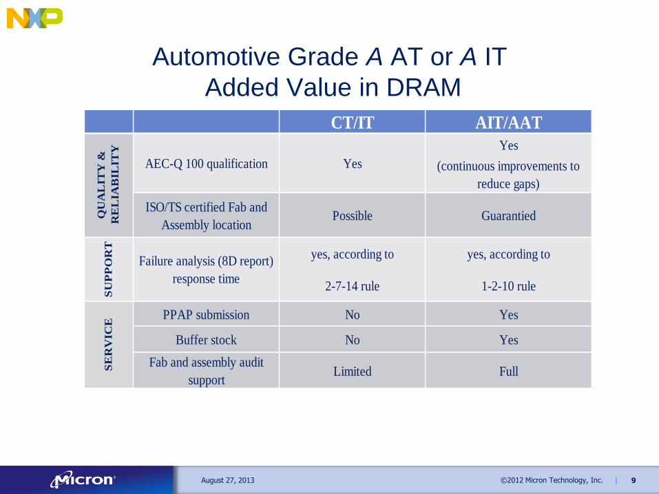
Automotive Grade A AT or A IT
Added Value in DRAM
CT/IT AIT/AAT
Yes
(continuous improvements to
reduce gaps)
ISO/TS certified Fab and
Assembly location Possible Guarantied
yes, according to yes, according to
2-7-14 rule 1-2-10 rule
PPAP submission No Yes
Buffer stock No Yes
Fab and assembly audit
support Limited Full S
ER
VIC
E
AEC-Q 100 qualification Yes
Failure analysis (8D report)
response time
QU
AL
ITY
&
RE
LIA
BIL
ITY
S
UP
PO
RT

10 ©2012 Micron Technology, Inc. | August 27, 2013
▶
System Power Comparison
11 ©2012 Micron Technology, Inc. |
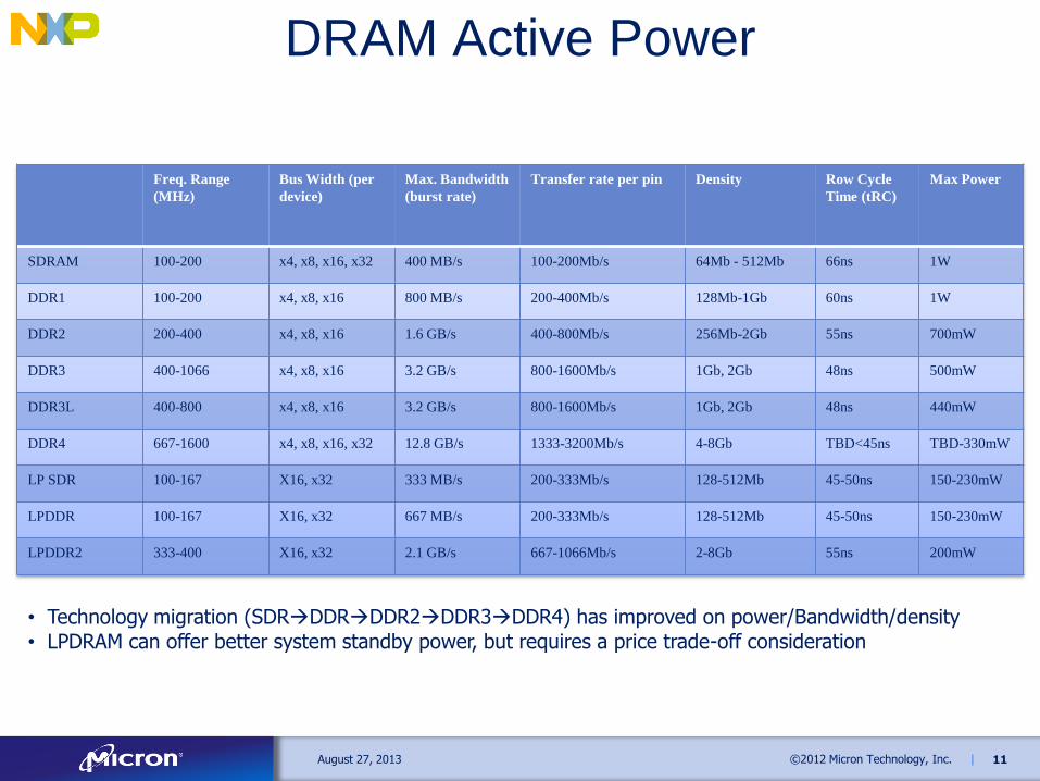
DRAM Active Power
Freq. Range
(MHz)
Bus Width (per
device)
Max. Bandwidth
(burst rate)
Transfer rate per pin Density Row Cycle
Time (tRC)
Max Power
SDRAM 100-200 x4, x8, x16, x32 400 MB/s 100-200Mb/s 64Mb - 512Mb 66ns 1W
DDR1 100-200 x4, x8, x16 800 MB/s 200-400Mb/s 128Mb-1Gb 60ns 1W
DDR2 200-400 x4, x8, x16 1.6 GB/s 400-800Mb/s 256Mb-2Gb 55ns 700mW
DDR3 400-1066 x4, x8, x16 3.2 GB/s 800-1600Mb/s 1Gb, 2Gb 48ns 500mW
DDR3L 400-800 x4, x8, x16 3.2 GB/s 800-1600Mb/s 1Gb, 2Gb 48ns 440mW
DDR4 667-1600 x4, x8, x16, x32 12.8 GB/s 1333-3200Mb/s 4-8Gb TBD<45ns TBD-330mW
LP SDR 100-167 X16, x32 333 MB/s 200-333Mb/s 128-512Mb 45-50ns 150-230mW
LPDDR 100-167 X16, x32 667 MB/s 200-333Mb/s 128-512Mb 45-50ns 150-230mW
LPDDR2 333-400 X16, x32 2.1 GB/s 667-1066Mb/s 2-8Gb 55ns 200mW
• Technology migration (SDRDDRDDR2DDR3DDR4) has improved on power/Bandwidth/density • LPDRAM can offer better system standby power, but requires a price trade-off consideration
August 27, 2013
12 ©2012 Micron Technology, Inc. | August 27, 2013
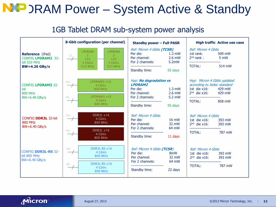
DRAM Power – System Active & Standby
LPDRAM
2
x32
4 Gbits
533 MHz
LPDRAM
2
x32
4 Gbits
533 MHz
Reference (iPad) CONFIG LPDRAM2 32-bit 533 MHz BW=4.26 GBy/s
32
CONFIG LPDRAM3 32-bit 800 MHz BW=6.40 GBy/s
DDR3L x16
4 Gbits
800 MHz
CONFIG DDR3L 32-bit 800 MHz BW=6.40 GBy/s
16U
DDR3L x16
4 Gbits
800 MHz
16L
Standby power – Full PASR 8-Gbit configuration (per channel)
Ref: Micron 4 Gbits (TCSR) Per die: 1.3 mW Per channel: 2.6 mW For 2 channels: 5.2mW ------------------------- Standby time: 55 days
Hyp: No degradation vs LPDRAM2 Per die: 1.3 mW Per channel: 2.6 mW For 2 channels: 5.2 mW ------------------------- Standby time: 55 days
Ref: Micron 4 Gbits Per die: 16 mW Per channel: 32 mW For 2 channels: 64 mW -------------------------- Standby time: 11 days
High traffic Active use case
Ref: Micron 4 Gbits 1st die x16: 393 mW 2nd die x16: 393 mW ------------------------- TOTAL: 787 mW
Ref: Micron 4 Gbits 1st rank: 509 mW 2nd rank : 5 mW ------------------------- TOTAL: 514 mW
Hyp: Micron 4 Gbits updated according to Jedec standard 1st die x16: 429 mW 2nd die x16: 429 mW ------------------------- TOTAL: 858 mW
LPDRAM3 x16
4 Gbits
800 MHz
16U
LPDRAM3 x16
4 Gbits
800 MHz
16L
1GB Tablet DRAM sub-system power analysis
DDR3L-RS x16
4 Gbits
800 MHz
CONFIG DDR3L-RS 32-bit 800 MHz BW=6.40 GBy/s
16U
DDR3L-RS x16
4 Gbits
800 MHz
16L
Ref: Micron 4 Gbits (TCSR) Per die: 8mW Per channel: 32 mW For 2 channels: 64 mW -------------------------- Standby time: 22 days
Ref: Micron 4 Gbits 1st die x16: 393 mW 2nd die x16: 393 mW ------------------------- TOTAL: 787 mW
13 ©2012 Micron Technology, Inc. | August 27, 2013
DRAM Cell and Architecture Overview
14 ©2012 Micron Technology, Inc. | August 27, 2013
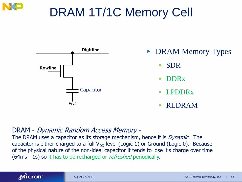
DRAM 1T/1C Memory Cell
▶ DRAM Memory Types
SDR
DDRx
LPDDRx
RLDRAM
Digitline
Rowline
Vref
DRAM - Dynamic Random Access Memory - The DRAM uses a capacitor as its storage mechanism, hence it is Dynamic. The capacitor is either charged to a full VDD level (Logic 1) or Ground (Logic 0). Because of the physical nature of the non-ideal capacitor it tends to lose it's charge over time (64ms - 1s) so it has to be recharged or refreshed periodically.
Capacitor
15 ©2012 Micron Technology, Inc. | August 27, 2013
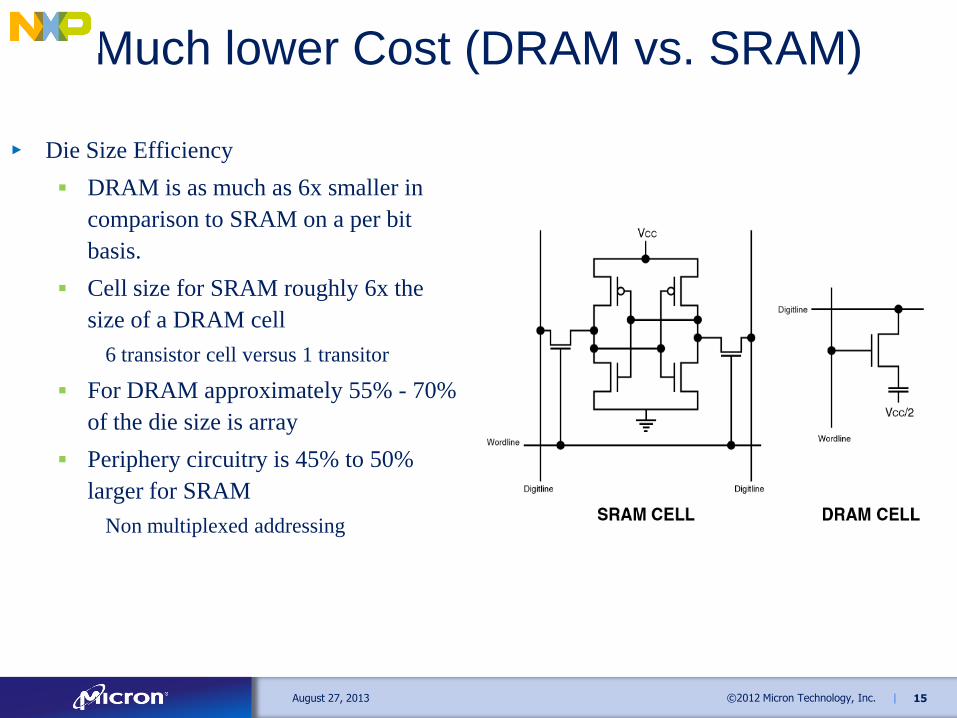
Much lower Cost (DRAM vs. SRAM)
▶ Die Size Efficiency
DRAM is as much as 6x smaller in
comparison to SRAM on a per bit
basis.
Cell size for SRAM roughly 6x the
size of a DRAM cell
6 transistor cell versus 1 transitor
For DRAM approximately 55% - 70%
of the die size is array
Periphery circuitry is 45% to 50%
larger for SRAM
Non multiplexed addressing
16 ©2012 Micron Technology, Inc. | August 27, 2013
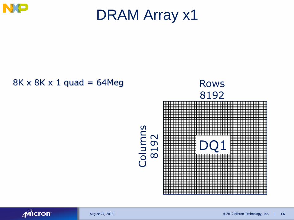
DRAM Array x1
Rows 8192
Colu
mns
8192
DQ1
8K x 8K x 1 quad = 64Meg
17 ©2012 Micron Technology, Inc. | August 27, 2013
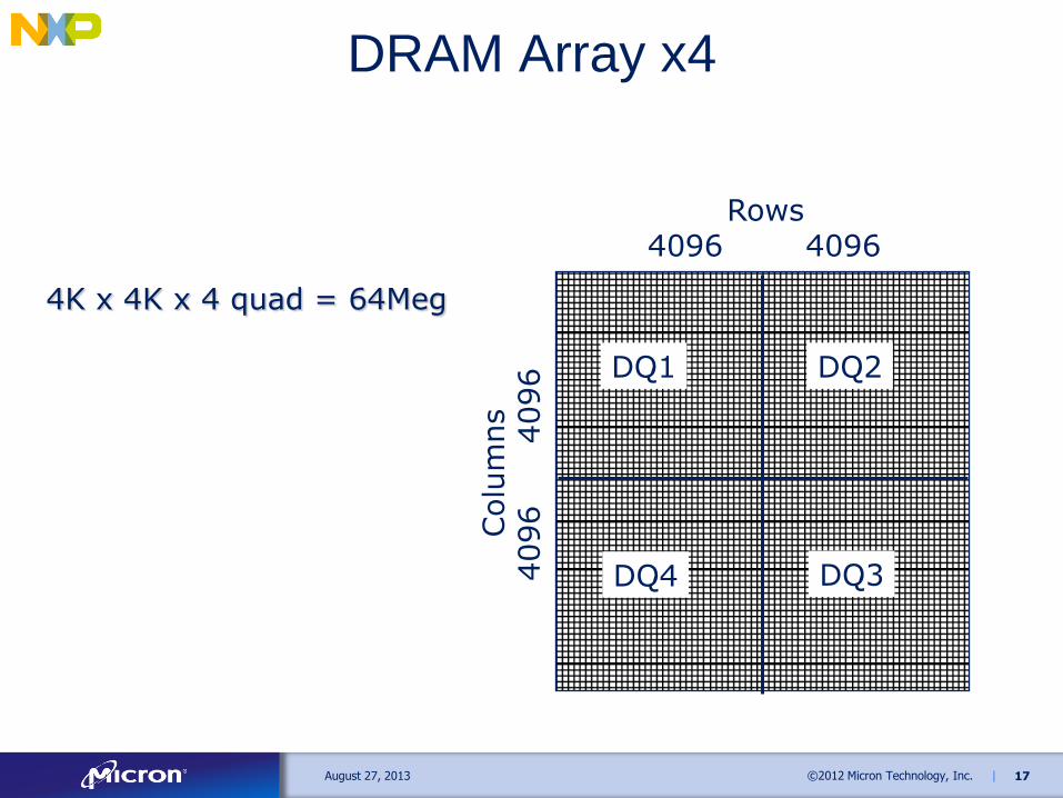
DRAM Array x4
Rows 4096 4096
Colu
mns
4096 4096 DQ1 DQ2
DQ3 DQ4
4K x 4K x 4 quad = 64Meg
18 ©2012 Micron Technology, Inc. | August 27, 2013
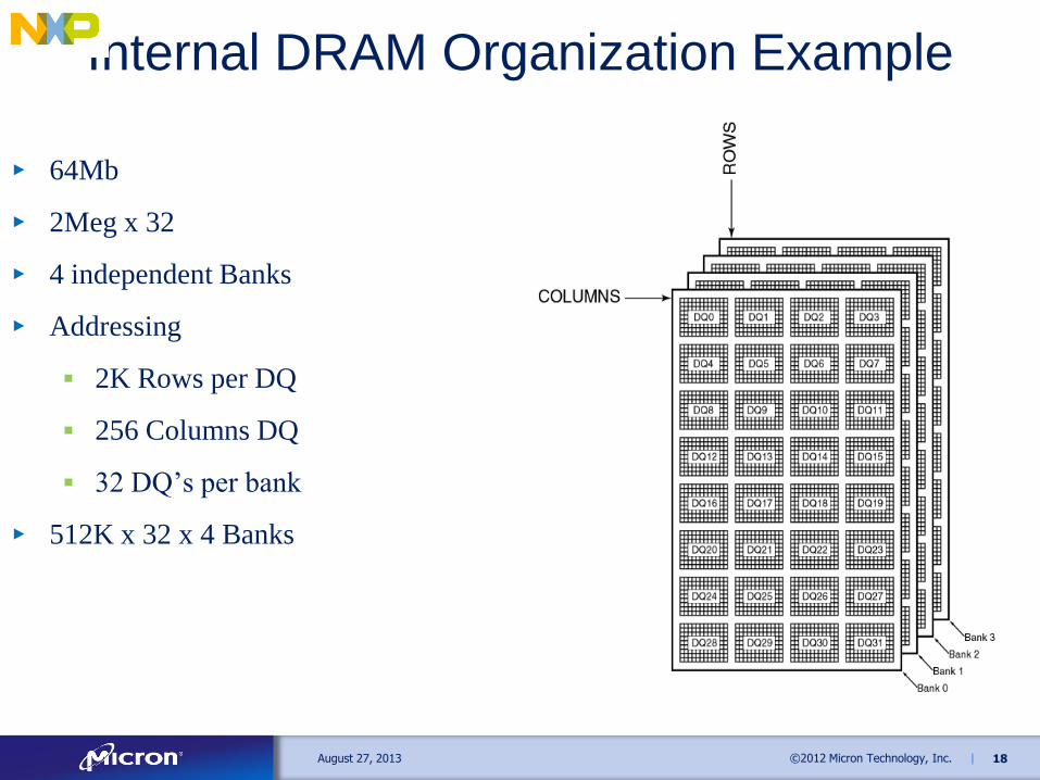
Internal DRAM Organization Example
▶ 64Mb
▶ 2Meg x 32
▶ 4 independent Banks
▶ Addressing
2K Rows per DQ
256 Columns DQ
32 DQ’s per bank
▶ 512K x 32 x 4 Banks
19 ©2012 Micron Technology, Inc. | August 27, 2013
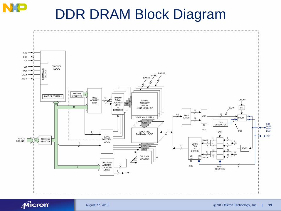
DDR DRAM Block Diagram
20 ©2012 Micron Technology, Inc. | August 27, 2013
Block Diagram Comparison
DDR2, DDR3, LPDDR2, LPDDR3
21 ©2012 Micron Technology, Inc. | August 27, 2013
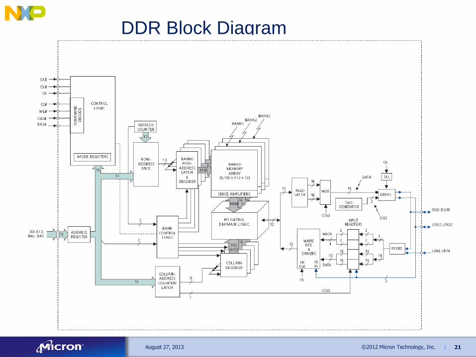
DDR Block Diagram
22 ©2012 Micron Technology, Inc. | August 27, 2013
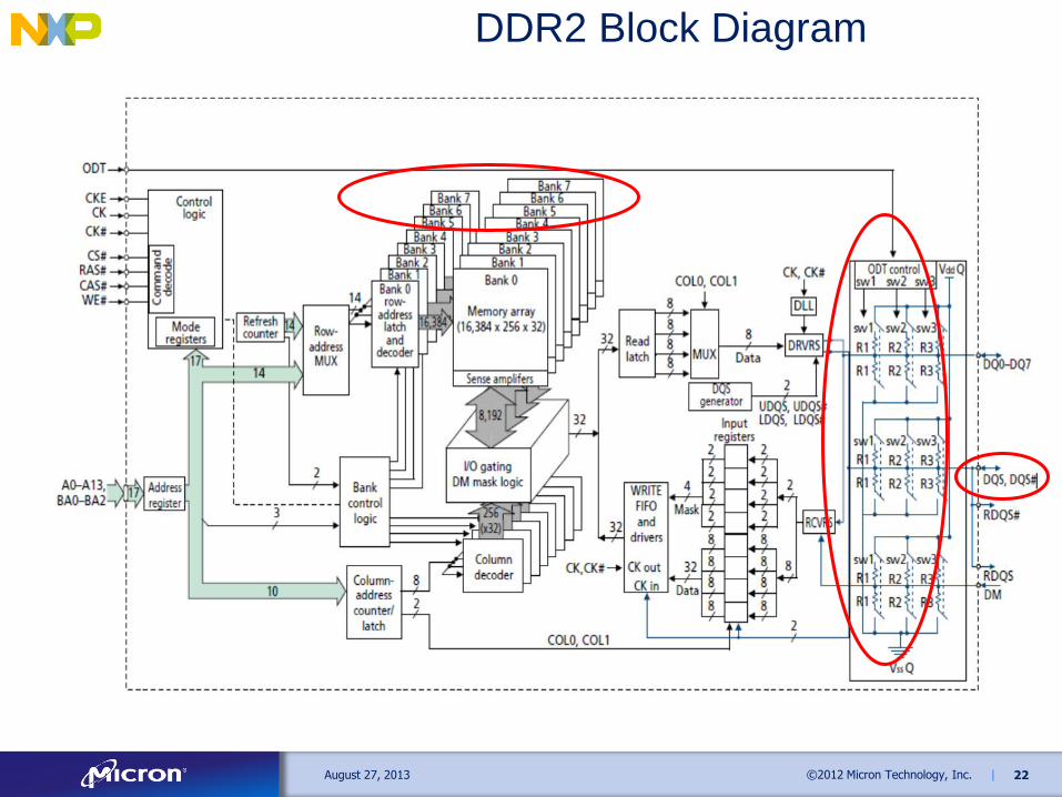
DDR2 Block Diagram
23 ©2012 Micron Technology, Inc. | August 27, 2013
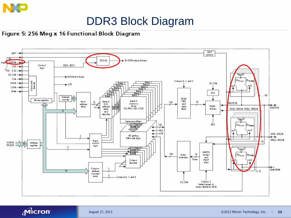
DDR3 Block Diagram
24 ©2012 Micron Technology, Inc. | August 27, 2013
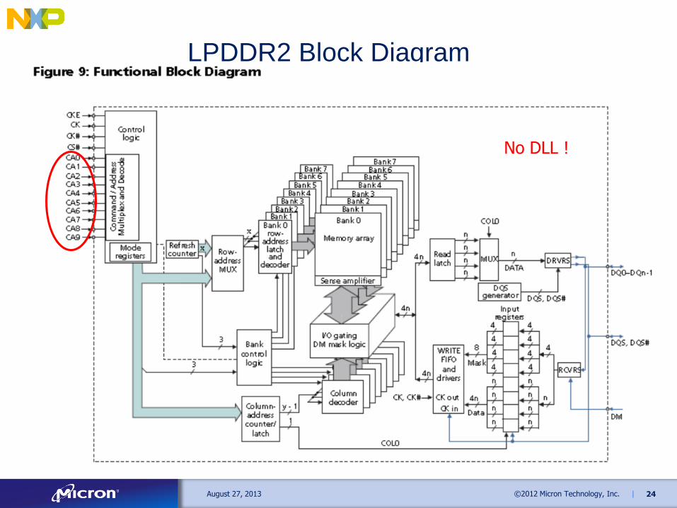
LPDDR2 Block Diagram
No DLL !
25 ©2012 Micron Technology, Inc. | August 27, 2013
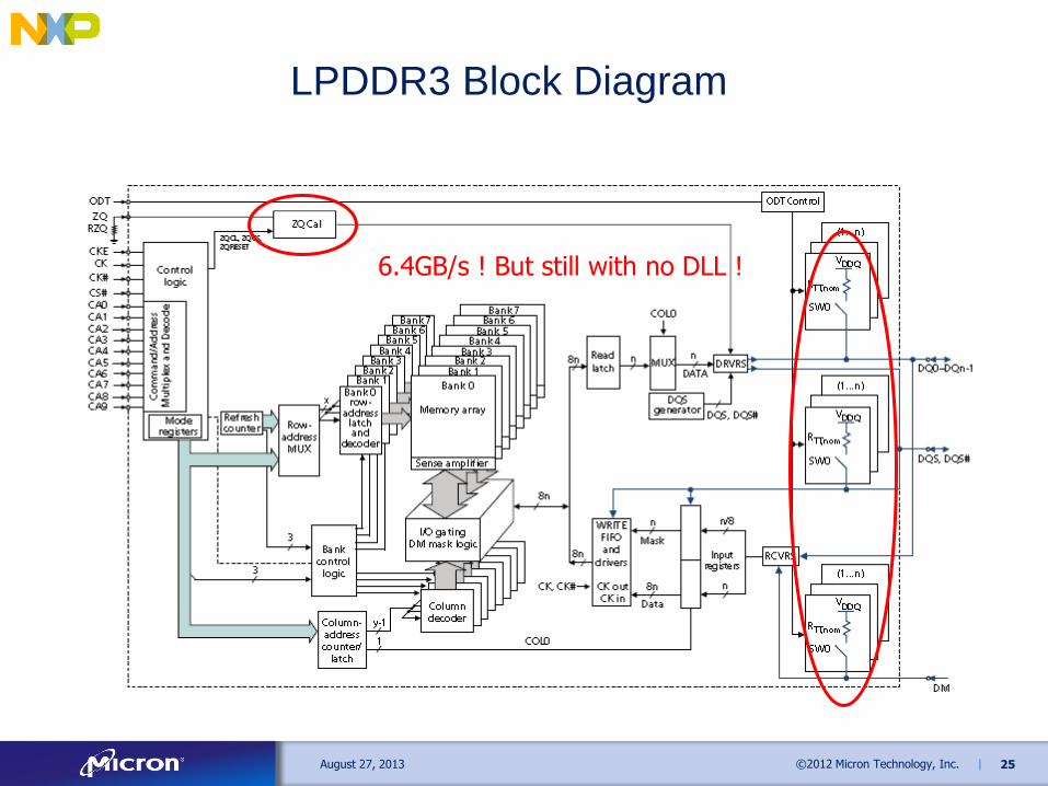
LPDDR3 Block Diagram
6.4GB/s ! But still with no DLL !
26 ©2012 Micron Technology, Inc. | August 27, 2013
Memory Initialization
Overview
• DDR3 Initialization Timing
• LPDDR2 Initialization Timing
27 ©2012 Micron Technology, Inc. |
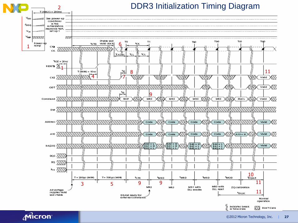
DDR3 Initialization Timing Diagram
1
2
1
3
4
5
6
7 8
9
10
9
9
11
11
11
29 ©2012 Micron Technology, Inc. | August 27, 2013
Mode Register Settings
• DDR3 Mode Registers MR0/MR1/MR2/MR3
• LPDDR2 Mode Registers MR0-255
30 ©2012 Micron Technology, Inc. |
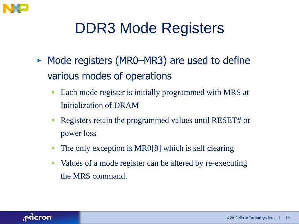
DDR3 Mode Registers
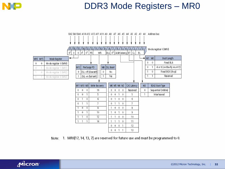
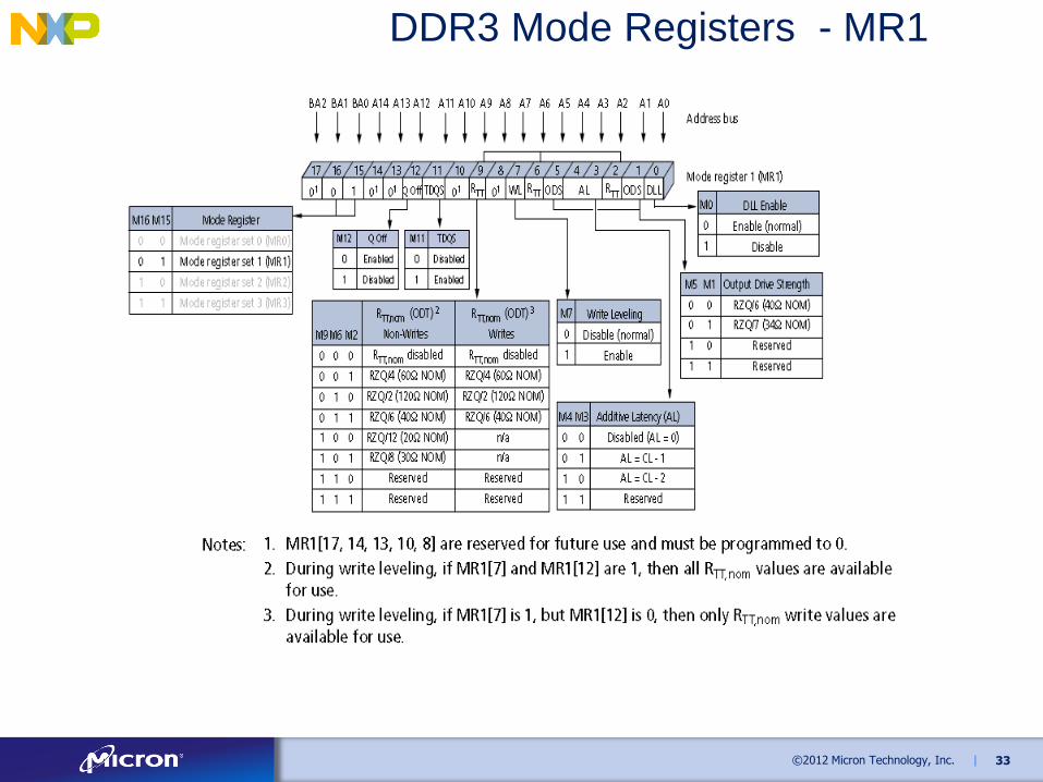
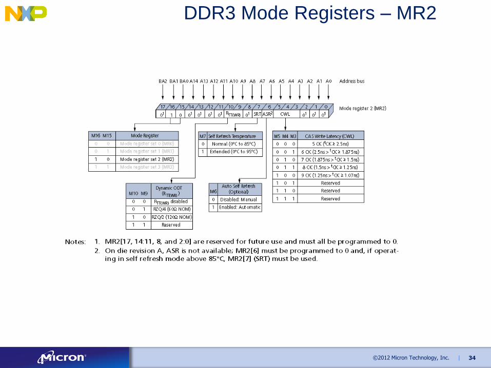
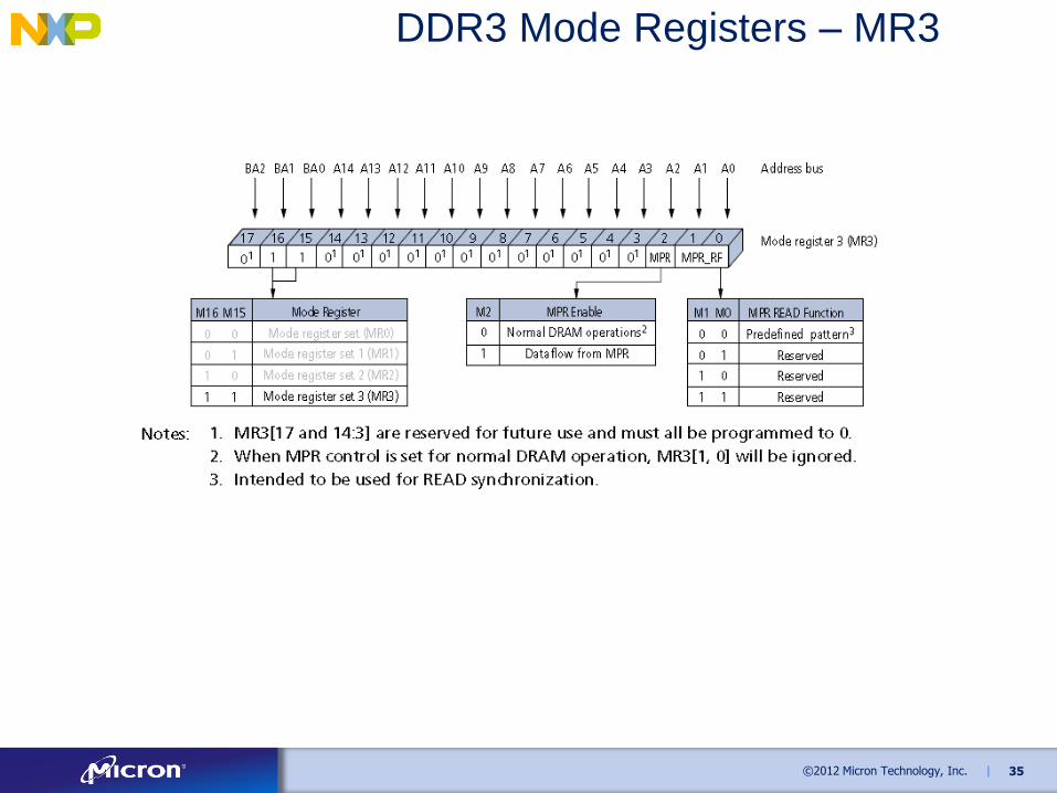
▶ Mode registers (MR0–MR3) are used to define
various modes of operations
Each mode register is initially programmed with MRS at
Initialization of DRAM
Registers retain the programmed values until RESET# or
power loss
The only exception is MR0[8] which is self clearing
Values of a mode register can be altered by re-executing
the MRS command.
32 ©2012 Micron Technology, Inc. |
DDR3 Mode Registers – MR0
33 ©2012 Micron Technology, Inc. |
DDR3 Mode Registers - MR1
34 ©2012 Micron Technology, Inc. |
DDR3 Mode Registers – MR2
35 ©2012 Micron Technology, Inc. |
DDR3 Mode Registers – MR3
38 ©2012 Micron Technology, Inc. |
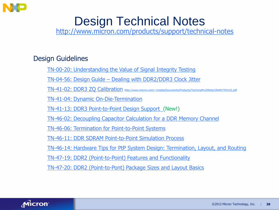
Design Technical Notes
Design Guidelines
TN-00-20: Understanding the Value of Signal Integrity Testing
TN-04-56: Design Guide – Dealing with DDR2/DDR3 Clock Jitter
TN-41-02: DDR3 ZQ Calibration http://www.micron.com/~/media/Documents/Products/Technical%20Note/DRAM/TN4102.pdf
TN-41-04: Dynamic On-Die-Termination
TN-41-13: DDR3 Point-to-Point Design Support (New!)
TN-46-02: Decoupling Capacitor Calculation for a DDR Memory Channel
TN-46-06: Termination for Point-to-Point Systems
TN-46-11: DDR SDRAM Point-to-Point Simulation Process
TN-46-14: Hardware Tips for PtP System Design: Termination, Layout, and Routing
TN-47-19: DDR2 (Point-to-Point) Features and Functionality
TN-47-20: DDR2 (Point-to-Pont) Package Sizes and Layout Basics
http://www.micron.com/products/support/technical-notes
39 ©2012 Micron Technology, Inc. |
Thanks!
40 ©2012 Micron Technology, Inc. |
Additional Reference Slides