micro and nano-processing technologies · the project report should have ... interdisciplinary...
TRANSCRIPT
Course objective:
Introduce the basic and advanced processing technologies that are used today in
modern micro-and nano fabrication cleanroom facilities.
It will present the fundamental principles of physics and science as a base to
understand different processing stages. This base is important in order to give a
knowledge e.g. for advanced decisions in process development and optimization.
Applications of each process should be carefully discussed to give an
understanding of limitations, restrictions and features on each processing step.
Micro and Nano-processing Technologies
Lectures and tutorials:
7,5 points total (200 h)
Lectures 28 (14x2) h.
Tutorials 3x2 h.
Problem solving (home assignments)
Project work 2,5 points (ca 65 h)
.
Literature
Chalmers Library
http://app.knovel.com/web/toc.v/cid:kpFEMNE001/viewerType:toc/root_slug:fabrication-engineering-at
Examination Requirements:
The student should be present on at least 80% percent of the lectures
and tutorials
Completed home assignments (hand in solutions of selected problems).
The problems will be submitted at 3 different occasions.
Completed project work (including oral presentation and written report)
Completed review work on another student’s written report.
.
Experimental Project:
Each student should plan and perform an experimental project related to the
processing technologies as presented in the course.
The objective of the project is to give the student a possibility to go deeper in the
understanding of a special processing step experimentally (or theoretically) but
also to get more experienced in process and project planning.
The project should be closely related to micro-and nano processing steps.
The results must be scrutinized and presented orally as well as in a written report

PROJECT ABSTRACT PROPOSAL (deadline 2nd February )
The topic of the project work should be described, including a preliminary time
schedule, written on max 1 page.
PROJECT REPORT (deadline 13th of March)
Describe the results of the work in a written report. The project report should have
a structure typical for a scientific conference paper (poster). This means a report
on 4 pages with double column, or 8 pages on standard format one column text
font 10, including a relevant number of figures of appropriate size.
It is recommended to hand in the report electronically as a PDF file. It is up to you
whether you like to include images, diagrams etc in the running text, or to put
those data as a supplement. However, it is recommended to use compressed
formats for pictures, etc.
The report should focus on the experimental/modelling results including a short
description of the techniques that were used. They should be described by your
own words and showing the general layout and also pinpointing parameters that
are critical for the outcome of the processing.

Oral presentation;
The project work should be presented by the student in an oral presentation,
at the final “mini-conference”, Friday 20th March.
10 minutes presentation followed by a 5 minutes discussion of each project.
the time for asking questions from the reviewers but also the audience is
recommended to participate.
The oral presentation should focus on presenting the results of the study. A
critical description of the possibilities and difficulties especially for the scope of
your work encountered is interesting.
It is not critically necessary to make a very deep description of the processing
equipments and techniques unless this information is important for the
understanding of the scope of the study.

Review report;
Each student will receive a project report from another student.
The student should review the report and address a few questions about the
content in the oral presentation session.
Each student should make a short written report of the questions and the
answers, and to be handed in to the course responsible (Ulf Södervall) e.g. by
email afterwards.

Assessment criteria:
The grade will be set according to the output of each student in these three
components as mentioned above and including also the home assignments.
Graduate students; Grades of ”passed” or ”non-passed” .
To reach level “Passed”, it requires the corresponding grade of 4 in
undergraduate education.
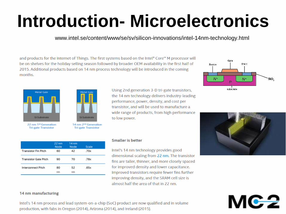
Introduction- Microelectronics• http://www.intel.se/content/www/se/sv/silicon-innovations/intel-14nm-technology.html
• INTEL ”Buzz” words in ”Microelectronics”
Smaller, Cheaper, Stronger
Eco- lead free
Energy saver/efficiency
Climate saver/ Sustainable
Halogen free
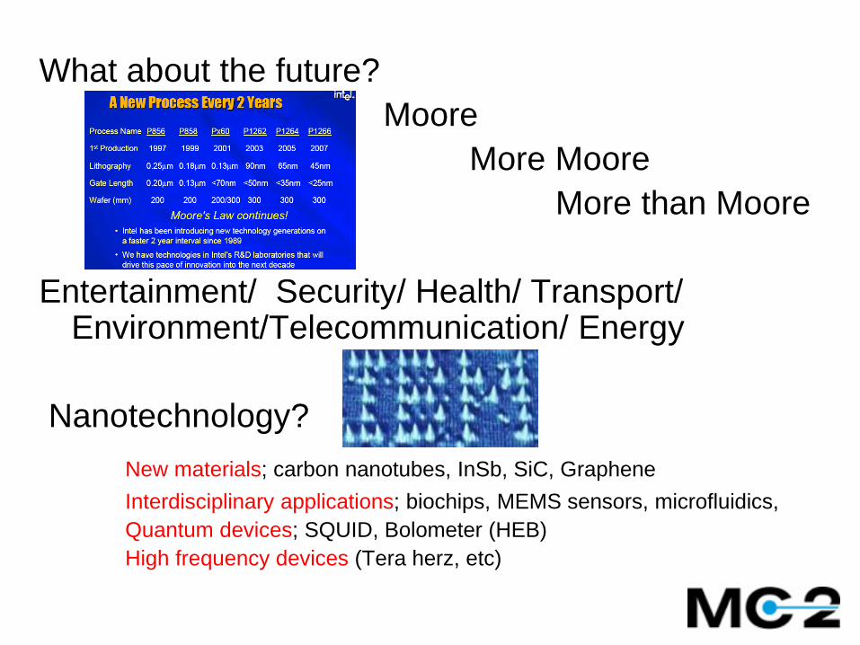
What about the future?
Moore
More Moore
More than Moore
Entertainment/ Security/ Health/ Transport/ Environment/Telecommunication/ Energy
Nanotechnology?
New materials; carbon nanotubes, InSb, SiC, Graphene
Interdisciplinary applications; biochips, MEMS sensors, microfluidics,
Quantum devices; SQUID, Bolometer (HEB)
High frequency devices (Tera herz, etc)


Micro Nano Process technology
Discrete devices vs. Integrated circuits“Semiconductor” device fabrication is the process used to create chips, the
integrated circuits that are present in everyday electrical and electronic devices.
It is a multiple-step sequence of photographic and chemical processing steps
during which electronic circuits are gradually created on a wafer made of pure
semiconductor material.
Once the wafers are prepared, a large number of process steps are necessary to
produce the desired semiconductor integrated circuits. In general the steps can be
grouped into four areas:
Front End Processing
Back End Processing
Test
Packaging.
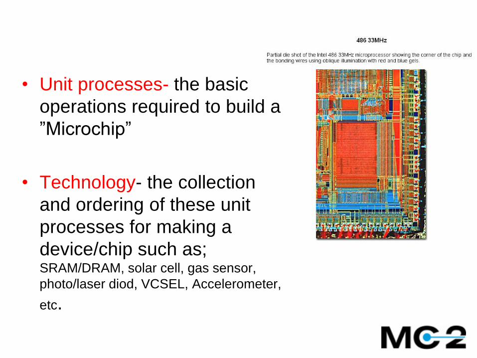
• Unit processes- the basic
operations required to build a
”Microchip”
• Technology- the collection
and ordering of these unit
processes for making a
device/chip such as;SRAM/DRAM, solar cell, gas sensor,
photo/laser diod, VCSEL, Accelerometer,
etc.
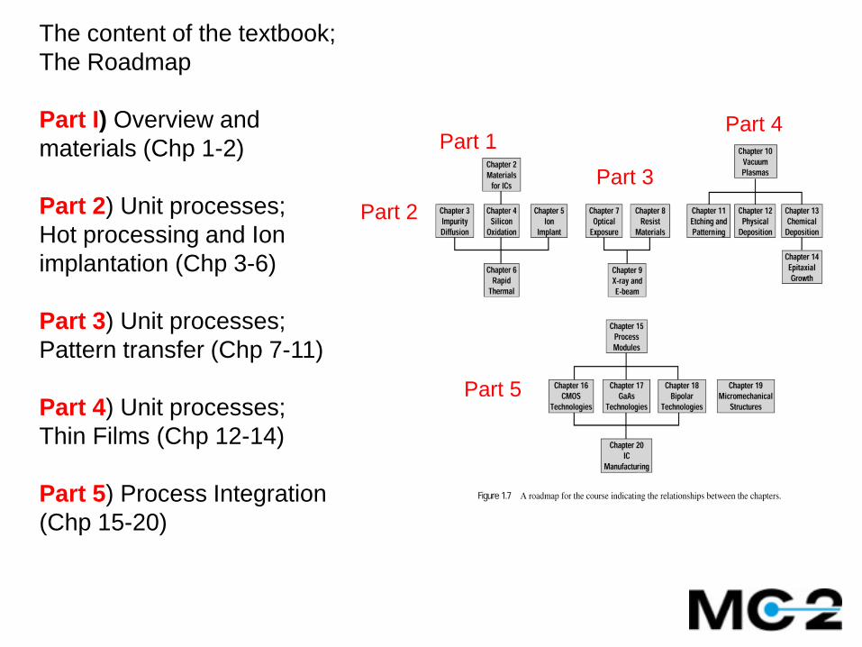
The content of the textbook;
The Roadmap
Part I) Overview and
materials (Chp 1-2)
Part 2) Unit processes;
Hot processing and Ion
implantation (Chp 3-6)
Part 3) Unit processes;
Pattern transfer (Chp 7-11)
Part 4) Unit processes;
Thin Films (Chp 12-14)
Part 5) Process Integration
(Chp 15-20)
Part 1
Part 2
Part 3
Part 4
Part 5
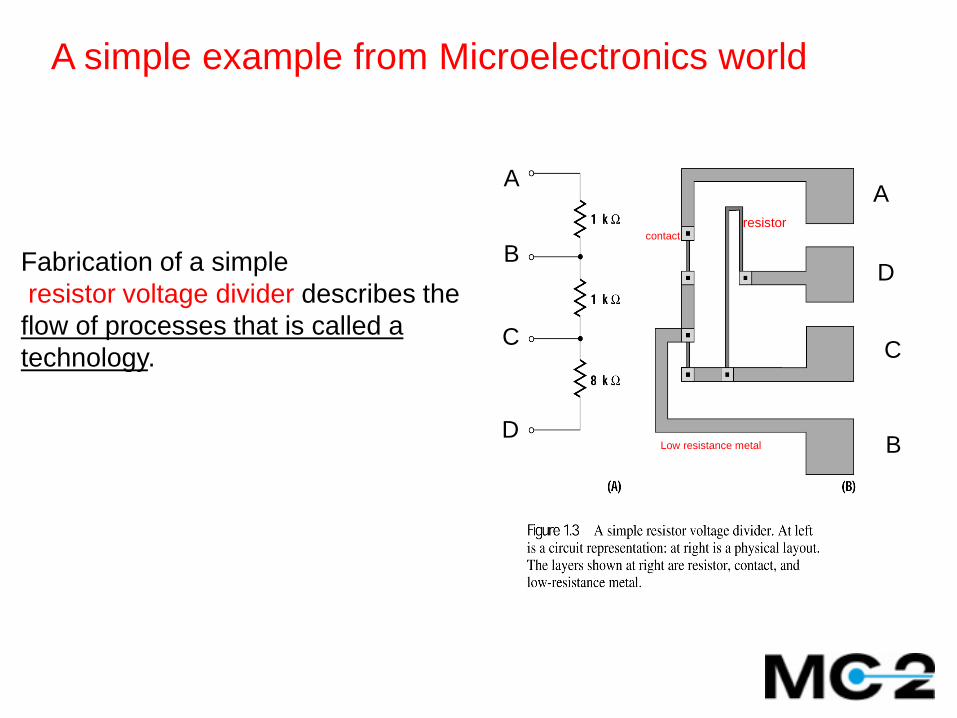
Fabrication of a simple
resistor voltage divider describes the
flow of processes that is called a
technology.
resistor
Low resistance metal
contact
A
B
C
D
A
B
C
D
A simple example from Microelectronics world
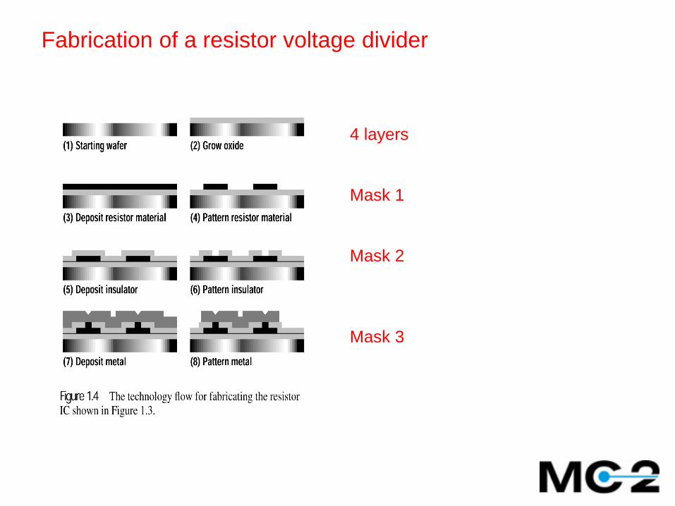
Fabrication of a resistor voltage divider
4 layers
Mask 1
Mask 2
Mask 3
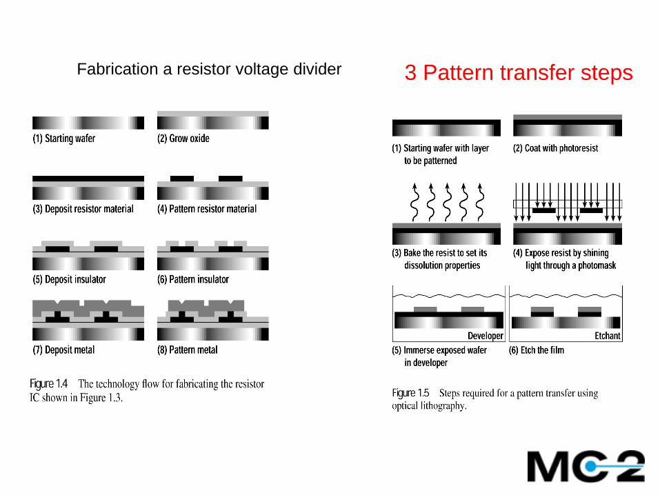
Fabrication a resistor voltage divider 3 Pattern transfer steps
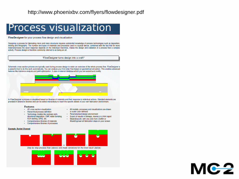
http://www.phoenixbv.com/flyers/flowdesigner.pdf
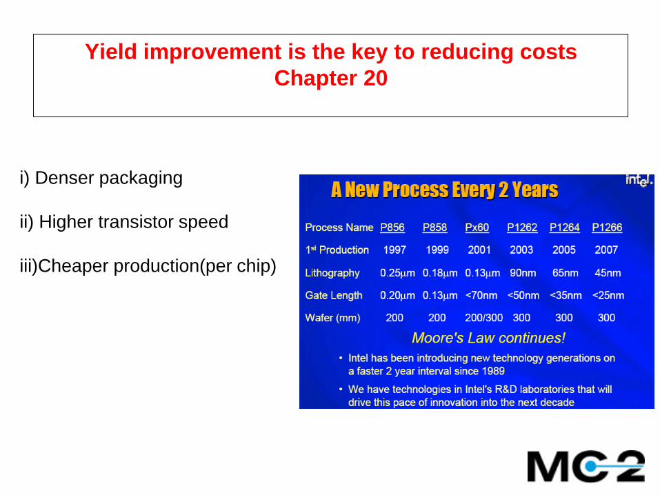
Yield improvement is the key to reducing costs
Chapter 20
i) Denser packaging
ii) Higher transistor speed
iii)Cheaper production(per chip)
The ultimate goal of these technologies is to be able to manufacture
functional components at high volume and low cost!
Definition of Yield ; The percentage of possible devices that are successfully fabricated, packaged and tested
Yield limiters:Number of process steps
Wafer breakage and warping
Process variation
Process defects
Mask defects
Example;
If we like to have a chip yield=50% for a 20 transistor circuit?!
0,50= X20
The individual transistor functionality, X, must be 96,6 %!
Integrated Circuit Manufacturing (Chp 20.1-20.3)
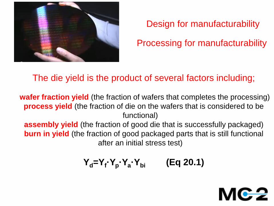
The die yield is the product of several factors including;
wafer fraction yield (the fraction of wafers that completes the processing)
process yield (the fraction of die on the wafers that is considered to be
functional)
assembly yield (the fraction of good die that is successfully packaged)
burn in yield (the fraction of good packaged parts that is still functional
after an initial stress test)
Yd=Yf·Yp·Ya·Ybi (Eq 20.1)
Design for manufacturability
Processing for manufacturability
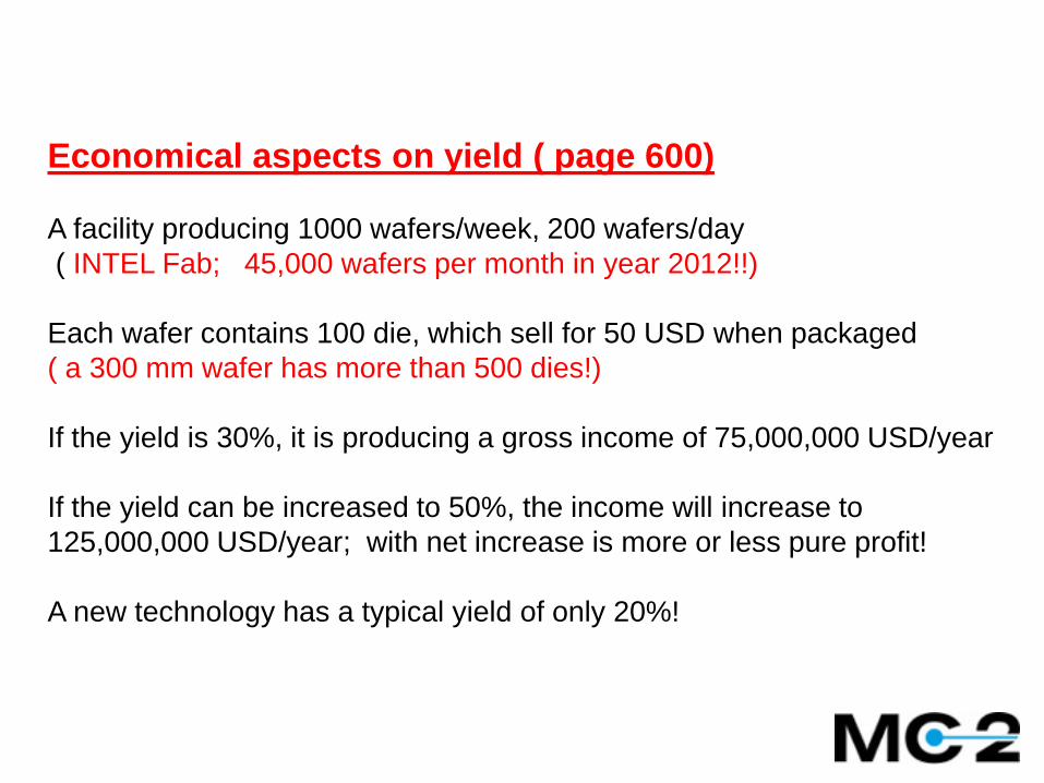
Economical aspects on yield ( page 600)
A facility producing 1000 wafers/week, 200 wafers/day
( INTEL Fab; 45,000 wafers per month in year 2012!!)
Each wafer contains 100 die, which sell for 50 USD when packaged
( a 300 mm wafer has more than 500 dies!)
If the yield is 30%, it is producing a gross income of 75,000,000 USD/year
If the yield can be increased to 50%, the income will increase to
125,000,000 USD/year; with net increase is more or less pure profit!
A new technology has a typical yield of only 20%!
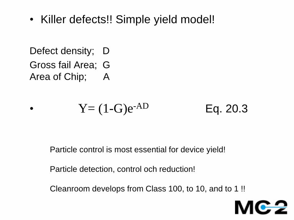
• Killer defects!! Simple yield model!
Defect density; D
Gross fail Area; G
Area of Chip; A
• Eq. 20.3
Particle control is most essential for device yield!
Particle detection, control och reduction!
Cleanroom develops from Class 100, to 10, and to 1 !!
Y= (1-G)e-AD
Lecture 1
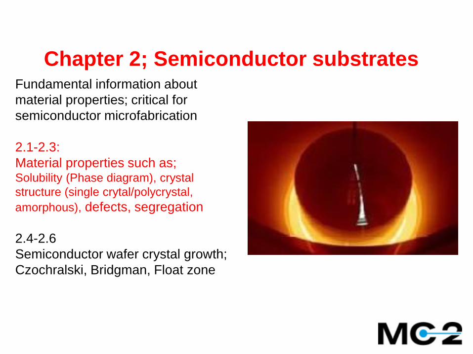
Fundamental information about
material properties; critical for
semiconductor microfabrication
2.1-2.3:
Material properties such as;Solubility (Phase diagram), crystal
structure (single crytal/polycrystal,
amorphous), defects, segregation
2.4-2.6
Semiconductor wafer crystal growth;
Czochralski, Bridgman, Float zone
Chapter 2; Semiconductor substrates
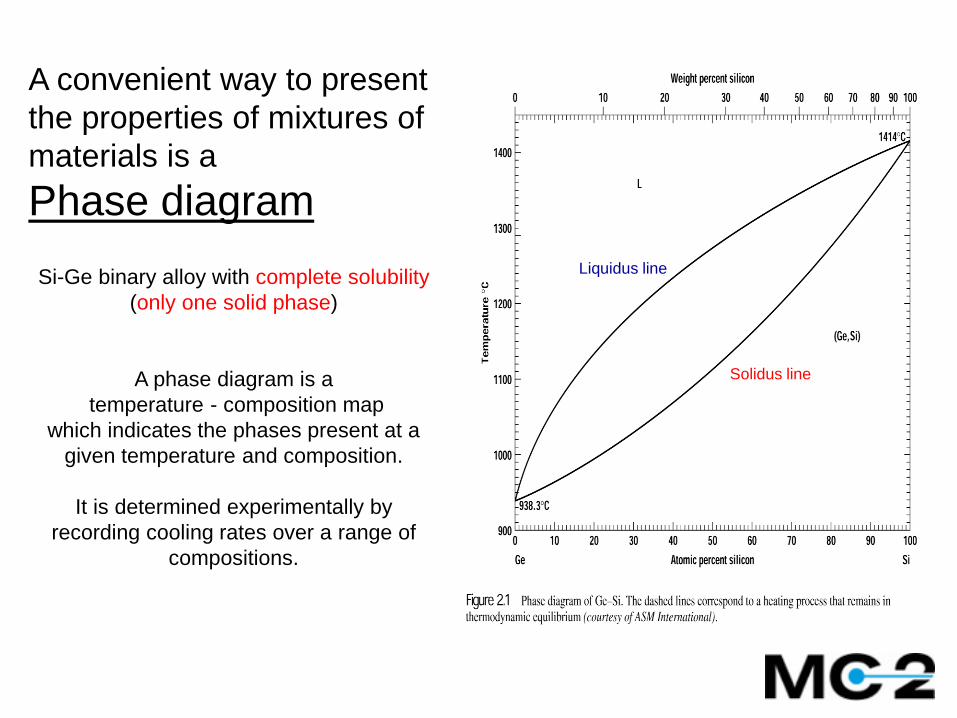
A convenient way to present
the properties of mixtures of
materials is a
Phase diagram
Si-Ge binary alloy with complete solubility
(only one solid phase)
A phase diagram is a
temperature - composition map
which indicates the phases present at a
given temperature and composition.
It is determined experimentally by
recording cooling rates over a range of
compositions.
Liquidus line
Solidus line
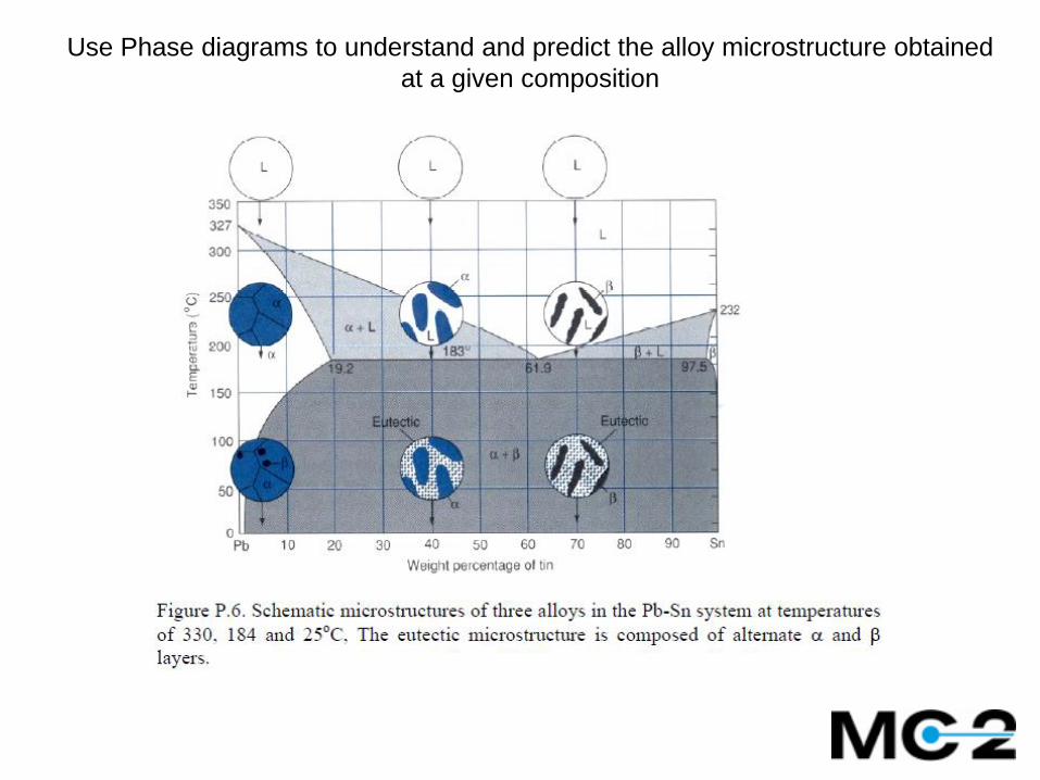
Use Phase diagrams to understand and predict the alloy microstructure obtained
at a given composition
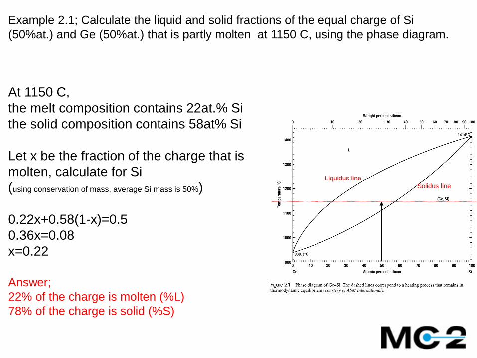
At 1150 C,
the melt composition contains 22at.% Si
the solid composition contains 58at% Si
Let x be the fraction of the charge that is
molten, calculate for Si
(using conservation of mass, average Si mass is 50%)
0.22x+0.58(1-x)=0.5
0.36x=0.08
x=0.22
Answer;
22% of the charge is molten (%L)
78% of the charge is solid (%S)
Solidus line
Liquidus line
Example 2.1; Calculate the liquid and solid fractions of the equal charge of Si
(50%at.) and Ge (50%at.) that is partly molten at 1150 C, using the phase diagram.
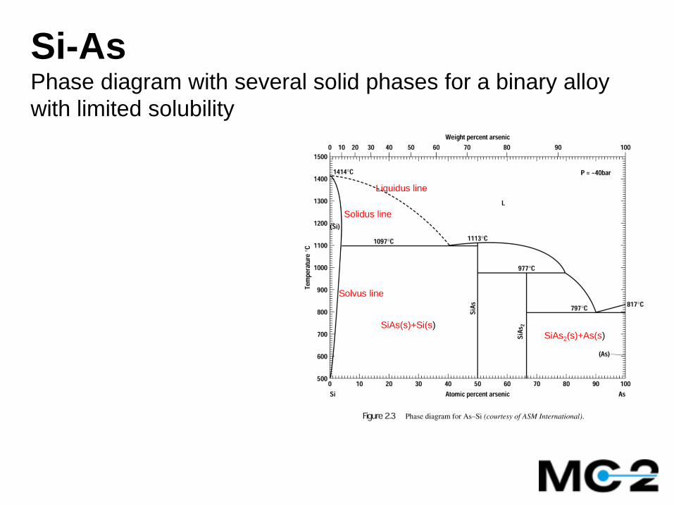
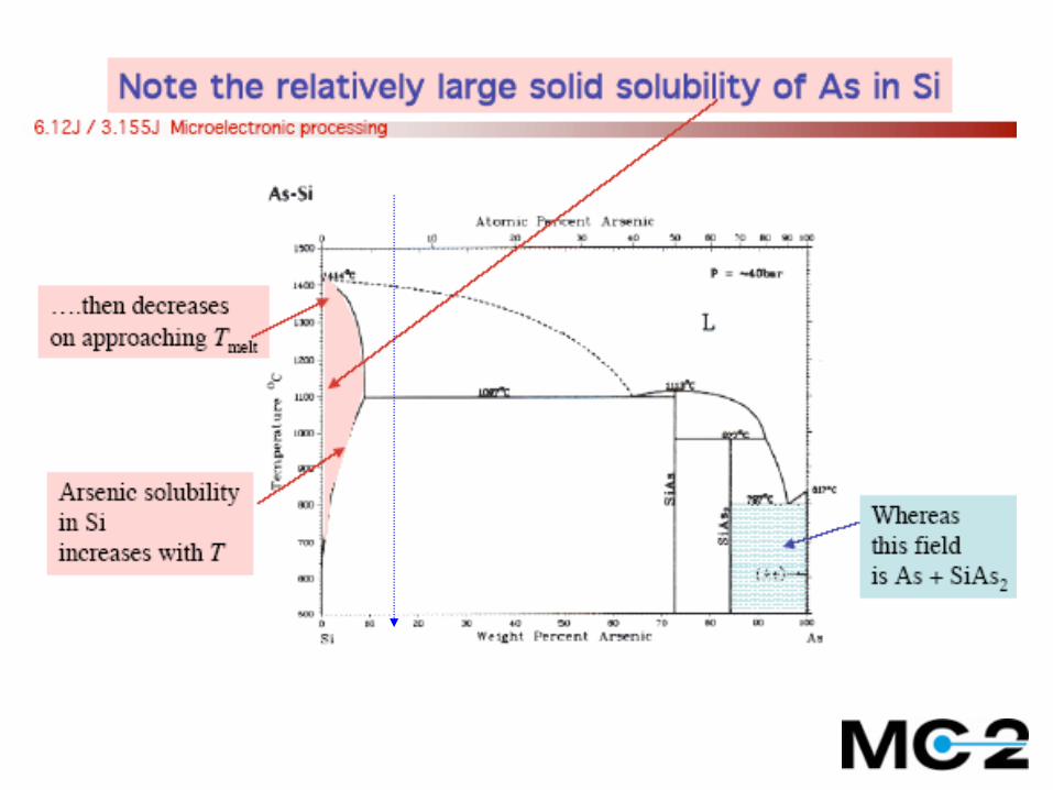
Si-AsPhase diagram with several solid phases for a binary alloy
with limited solubility
Liquidus line
Solvus line
Solidus line
SiAs(s)+Si(s)SiAs2(s)+As(s)
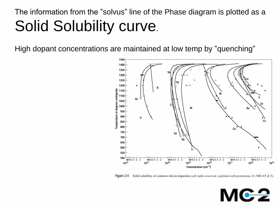
The information from the ”solvus” line of the Phase diagram is plotted as a
Solid Solubility curve.
High dopant concentrations are maintained at low temp by ”quenching”
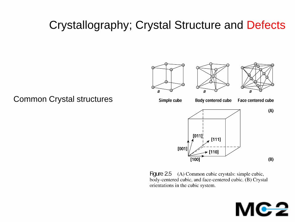
Common Crystal structures
Crystallography; Crystal Structure and Defects
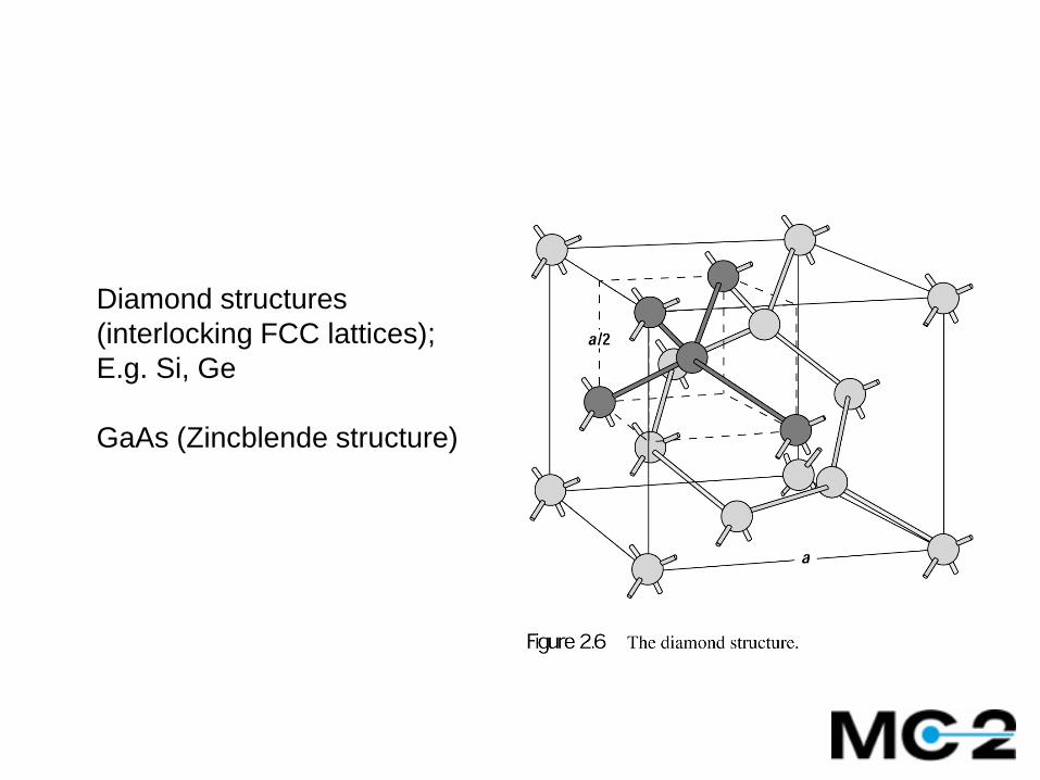
Diamond structures
(interlocking FCC lattices);
E.g. Si, Ge
GaAs (Zincblende structure)
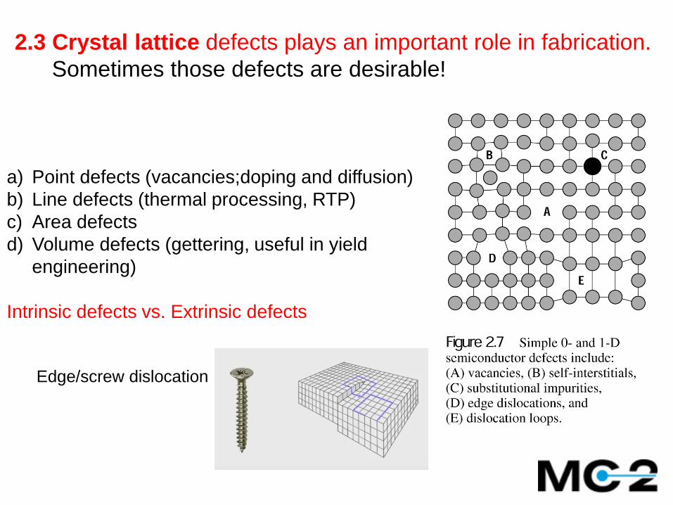
a) Point defects (vacancies;doping and diffusion)
b) Line defects (thermal processing, RTP)
c) Area defects
d) Volume defects (gettering, useful in yield
engineering)
Intrinsic defects vs. Extrinsic defects
2.3 Crystal lattice defects plays an important role in fabrication.
Sometimes those defects are desirable!
Edge/screw dislocation
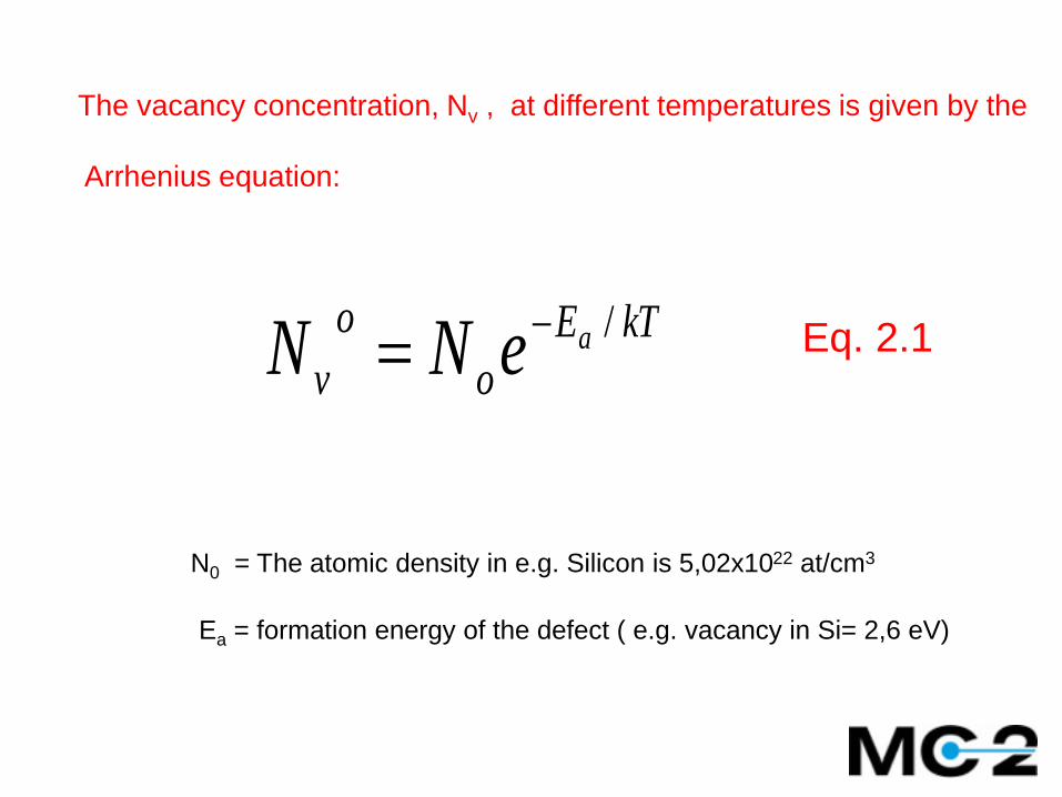
The vacancy concentration, Nv , at different temperatures is given by the
Arrhenius equation:
kTE
o
o
vaeNN
/
N0 = The atomic density in e.g. Silicon is 5,02x10²² at/cm3
Ea = formation energy of the defect ( e.g. vacancy in Si= 2,6 eV)
Eq. 2.1
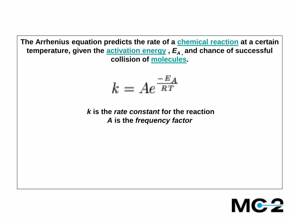
The Arrhenius equation predicts the rate of a chemical reaction at a certain
temperature, given the activation energy , EA , and chance of successful
collision of molecules.
k is the rate constant for the reaction
A is the frequency factor
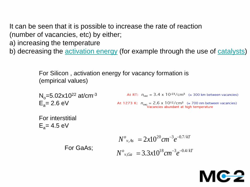
For Silicon , activation energy for vacancy formation is
(empirical values)
No=5.02x10²² at/cm-3
Ea= 2.6 eV
For interstitial
Ea= 4.5 eV
kTGav
o ecmxN /4.0318, 103.3
kTAsv
o ecmxN /7.0320, 102
For GaAs;
It can be seen that it is possible to increase the rate of reaction
(number of vacancies, etc) by either;
a) increasing the temperature
b) decreasing the activation energy (for example through the use of catalysts)
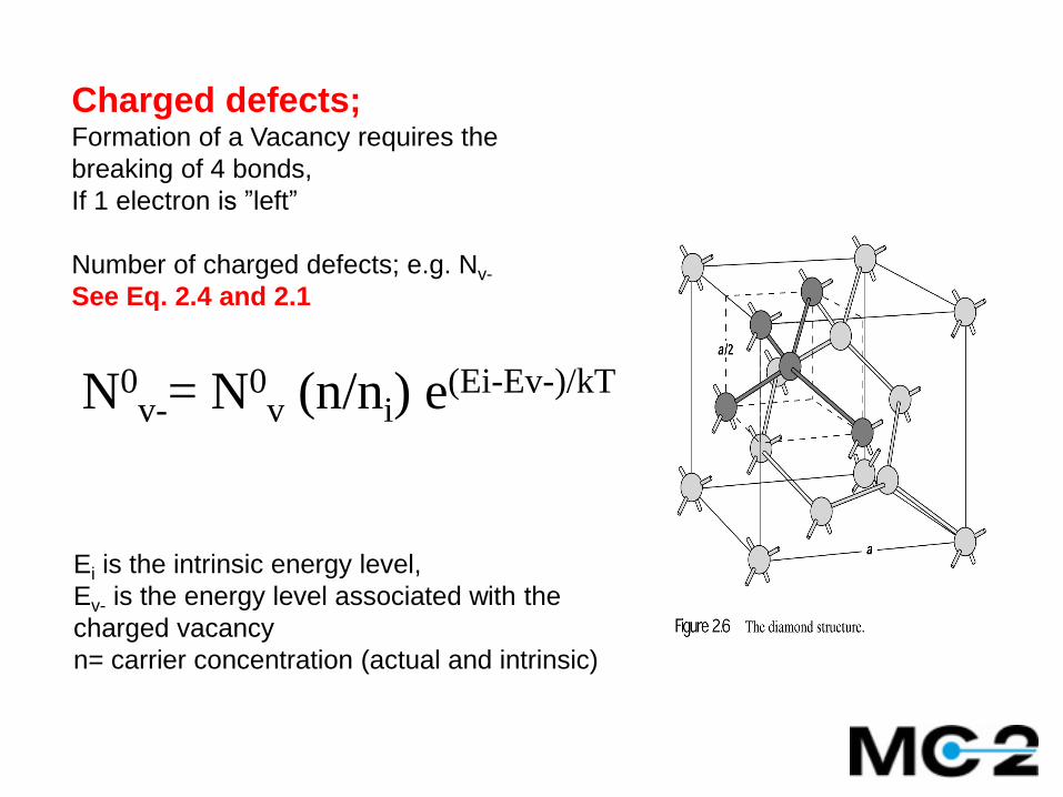
Charged defects;Formation of a Vacancy requires the
breaking of 4 bonds,
If 1 electron is ”left”
Number of charged defects; e.g. Nv-
See Eq. 2.4 and 2.1
Ei is the intrinsic energy level,
Ev- is the energy level associated with the
charged vacancy
n= carrier concentration (actual and intrinsic)
N0v-= N0
v (n/ni) e(Ei-Ev-)/kT
Gettering
The process of removing device-degrading impurities
from the active circuit regions of the wafer.
Gettering, which can be performed during crystal
growth or in subsequent wafer fabrication steps, is an
important ingredient for enhancing the yield of VLSI
manufacturing
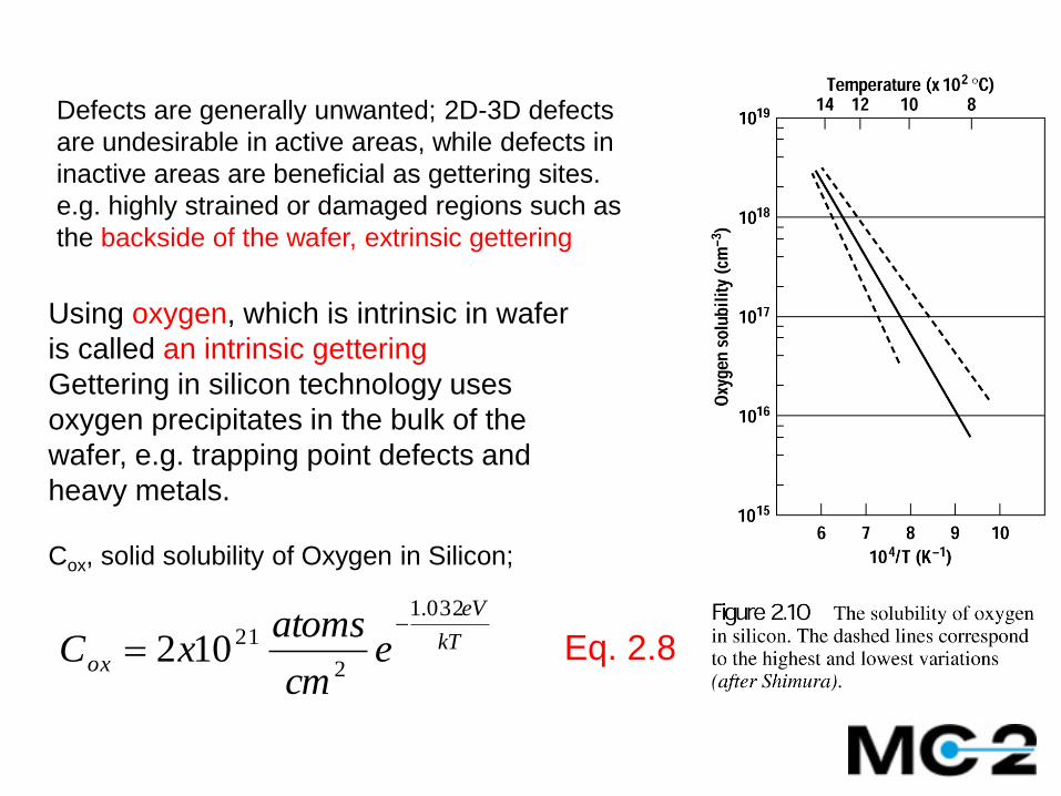
Using oxygen, which is intrinsic in wafer
is called an intrinsic gettering
Gettering in silicon technology uses
oxygen precipitates in the bulk of the
wafer, e.g. trapping point defects and
heavy metals.
Cox, solid solubility of Oxygen in Silicon;
kT
eV
ox ecm
atomsxC
032.1
2
21102
Defects are generally unwanted; 2D-3D defects
are undesirable in active areas, while defects in
inactive areas are beneficial as gettering sites.
e.g. highly strained or damaged regions such as
the backside of the wafer, extrinsic gettering
Eq. 2.8
Intrinsic gettering process requires an oxygen concentration of 15-20 ppm;
lower means to far away for precipitation
higher will lead to warpage, extended defects
A typical intrinsic gettering process consists of three steps;
outdiffusion, nucleation and precipitation
outdiffusion; (reduce concentration of dissolved oxygen in a denuded zone) by
annealing at high temperatures in an inert ambient (20-30 microns)
Eq. 2.9
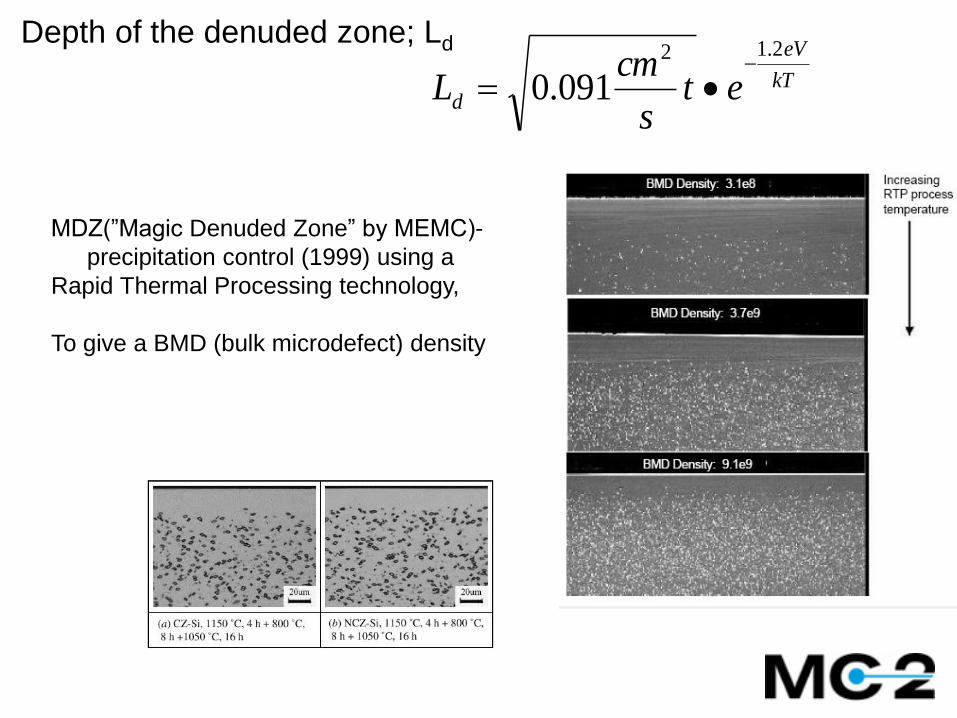
MDZ(”Magic Denuded Zone” by MEMC)-
precipitation control (1999) using a
Rapid Thermal Processing technology,
To give a BMD (bulk microdefect) density
kT
eV
d ets
cmL
2.12
091.0
Depth of the denuded zone; Ld

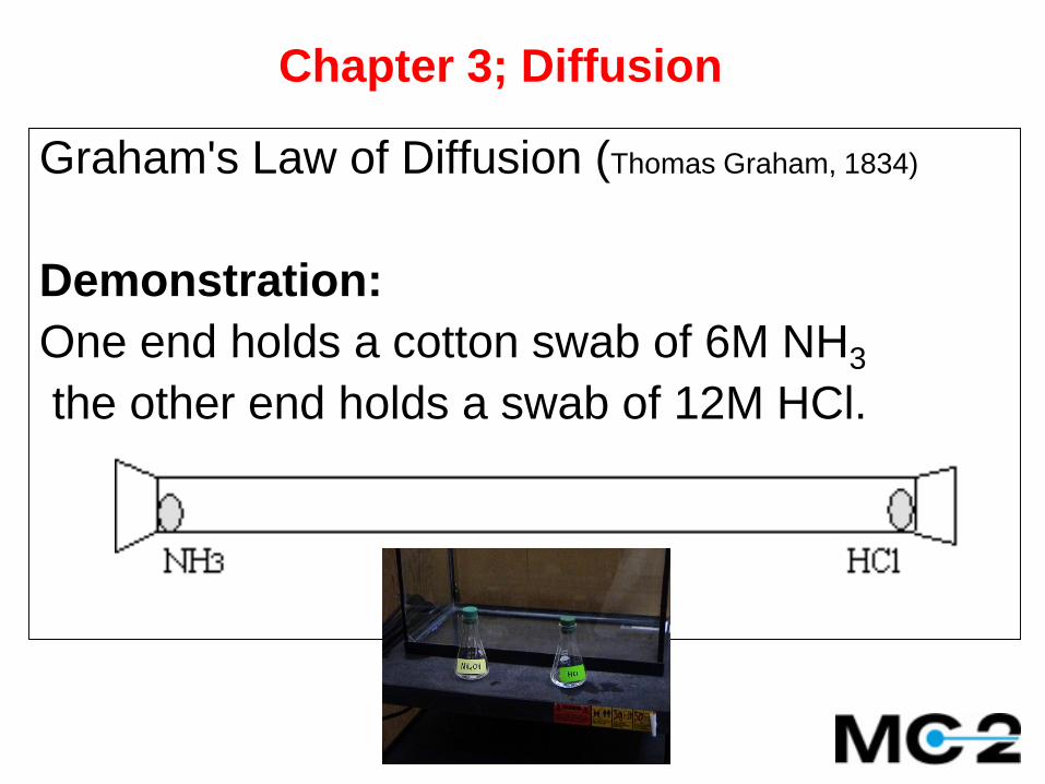
Graham's Law of Diffusion (Thomas Graham, 1834)
Demonstration:
One end holds a cotton swab of 6M NH3
the other end holds a swab of 12M HCl.
Chapter 3; Diffusion
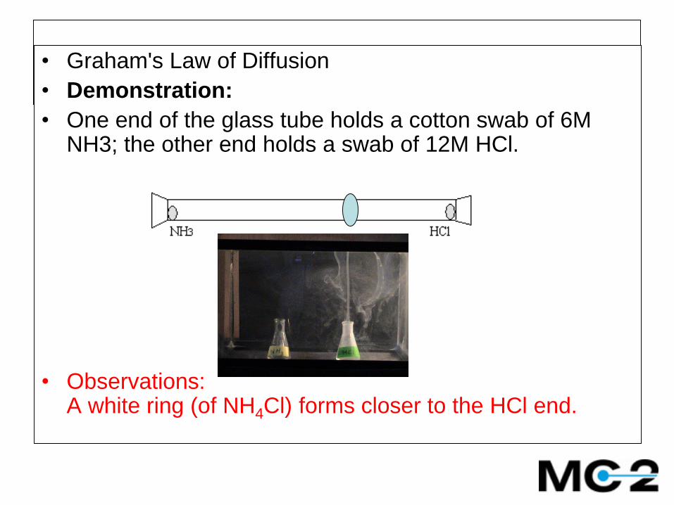
• Graham's Law of Diffusion
• Demonstration:
• One end of the glass tube holds a cotton swab of 6M NH3; the other end holds a swab of 12M HCl.
• Observations:A white ring (of NH4Cl) forms closer to the HCl end.
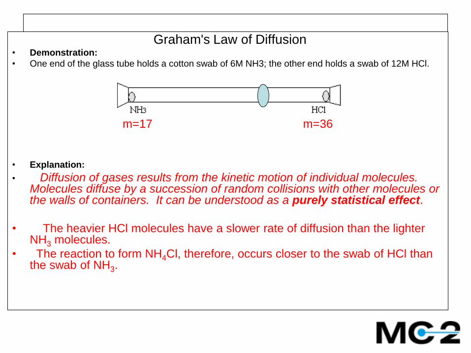
Graham's Law of Diffusion• Demonstration:
• One end of the glass tube holds a cotton swab of 6M NH3; the other end holds a swab of 12M HCl.
• Explanation:
• Diffusion of gases results from the kinetic motion of individual molecules. Molecules diffuse by a succession of random collisions with other molecules or the walls of containers. It can be understood as a purely statistical effect.
• The heavier HCl molecules have a slower rate of diffusion than the lighter NH3 molecules.
• The reaction to form NH4Cl, therefore, occurs closer to the swab of HCl than the swab of NH3.
m=36m=17

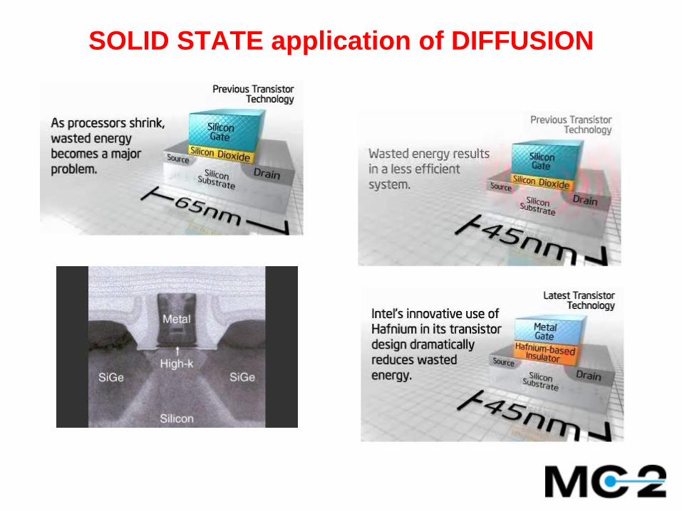
SOLID STATE application of DIFFUSION
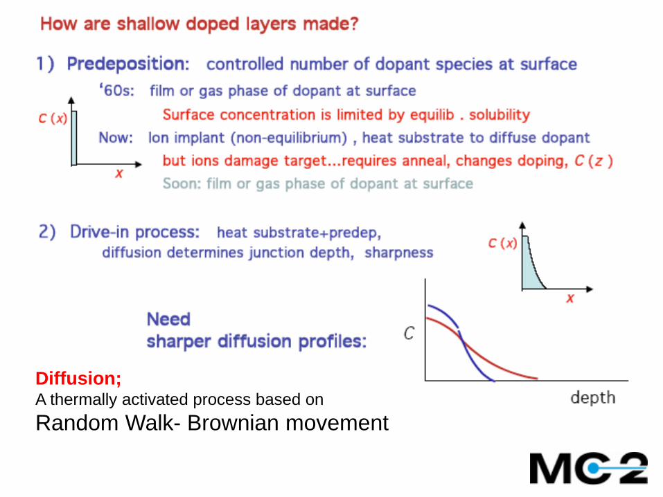
Diffusion;A thermally activated process based on
Random Walk- Brownian movement
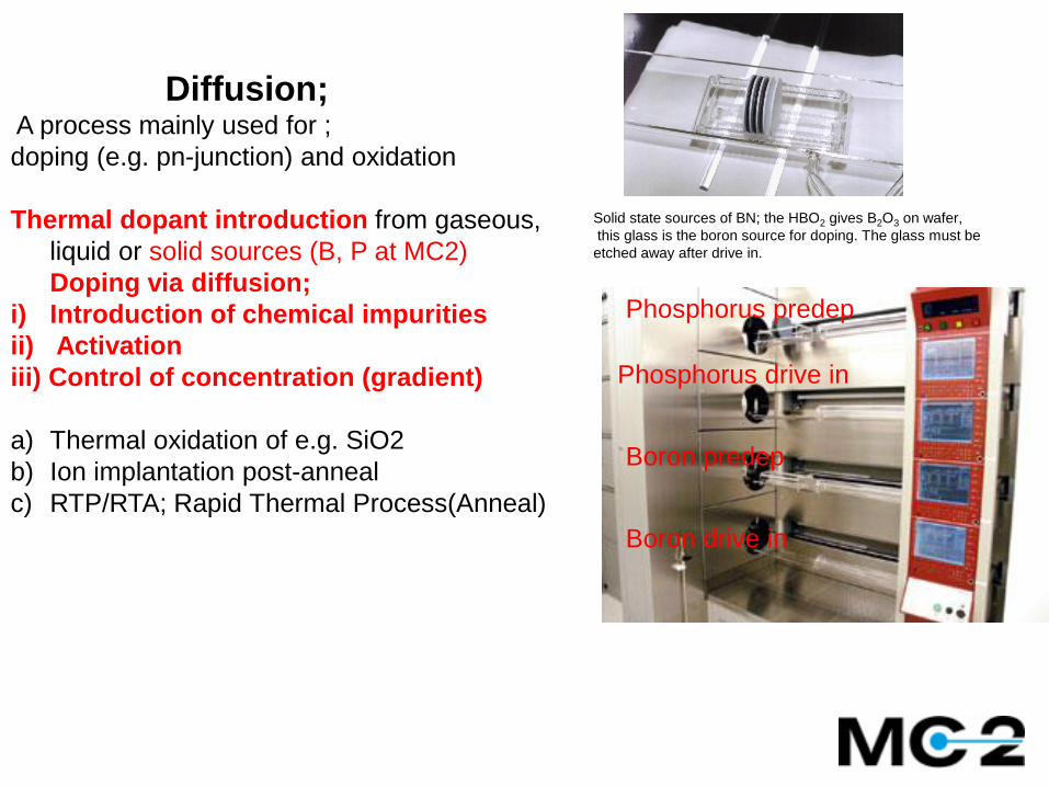
Diffusion;A process mainly used for ;
doping (e.g. pn-junction) and oxidation
Thermal dopant introduction from gaseous,
liquid or solid sources (B, P at MC2)
Doping via diffusion;
i) Introduction of chemical impurities
ii) Activation
iii) Control of concentration (gradient)
a) Thermal oxidation of e.g. SiO2
b) Ion implantation post-anneal
c) RTP/RTA; Rapid Thermal Process(Anneal)
Boron predep
Phosphorus predep
Boron drive in
Phosphorus drive in
Solid state sources of BN; the HBO2 gives B2O3 on wafer,
this glass is the boron source for doping. The glass must be
etched away after drive in.
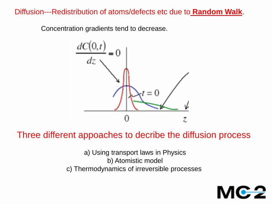
Three different appoaches to decribe the diffusion process
a) Using transport laws in Physics
b) Atomistic model
c) Thermodynamics of irreversible processes
Diffusion---Redistribution of atoms/defects etc due to Random Walk.
Concentration gradients tend to decrease.
x
txCDJ
),(
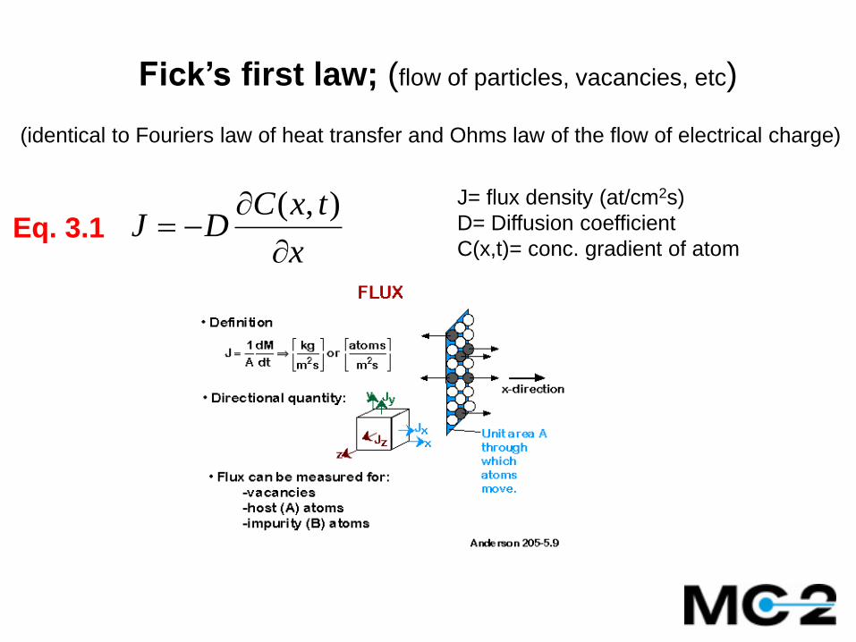
Fick’s first law; (flow of particles, vacancies, etc)
(identical to Fouriers law of heat transfer and Ohms law of the flow of electrical charge)
J= flux density (at/cm2s)
D= Diffusion coefficient
C(x,t)= conc. gradient of atomEq. 3.1
x
txCDJ
),(
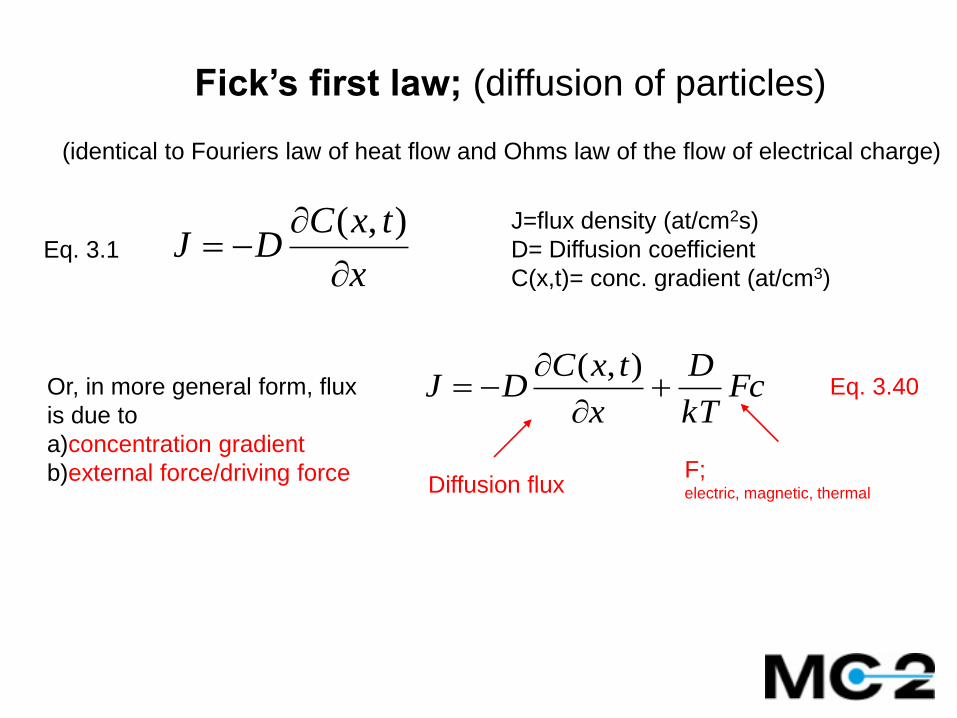
Fick’s first law; (diffusion of particles)
(identical to Fouriers law of heat flow and Ohms law of the flow of electrical charge)
J=flux density (at/cm2s)
D= Diffusion coefficient
C(x,t)= conc. gradient (at/cm3)
FckT
D
x
txCDJ
),(Or, in more general form, flux
is due to
a)concentration gradient
b)external force/driving forceDiffusion flux
F; electric, magnetic, thermal
Eq. 3.1
Eq. 3.40

x
txCDJ
),(
Fick’s first law; (diffusion of particles)
x
J
dx
JJ
12
However, not enough for measuring ”material flow”
at non- steady state conditions;
Eq. 3.1
Eq. 3.2
x
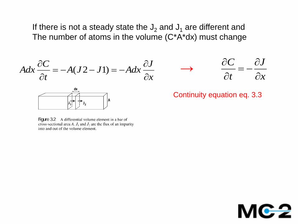
JAdxJJA
t
CAdx
)12(
If there is not a steady state the J2 and J1 are different and
The number of atoms in the volume (C*A*dx) must change
x
J
t
C
→
Continuity equation eq. 3.3

2
2 ),(),(
x
txCD
t
txC
x
JAdxJJA
t
CAdx
)12(
If there is not a steady state the J2 and J1 are different and
The number of atoms in the volume (C*A*dx) must change
x
J
t
C
→
x
J
t
C
+
x
txCDJ
),( →
Fick’s 2nd law, Eq. 3.4
Continuity equation eq. 3.3
Cont. Eq.; 3.3 Fick’s 1st law; Eq. 3.1
Whatabout D ?!
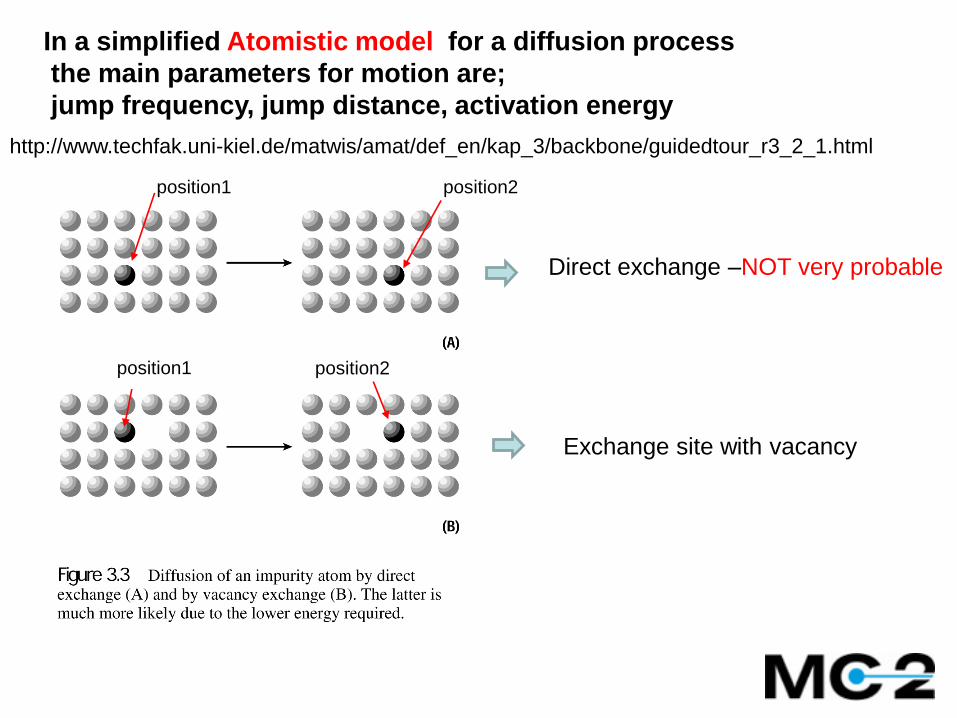
In a simplified Atomistic model for a diffusion process
the main parameters for motion are;
jump frequency, jump distance, activation energy
position1 position2
position1 position2
http://www.techfak.uni-kiel.de/matwis/amat/def_en/kap_3/backbone/guidedtour_r3_2_1.html
Direct exchange –NOT very probable
Exchange site with vacancy
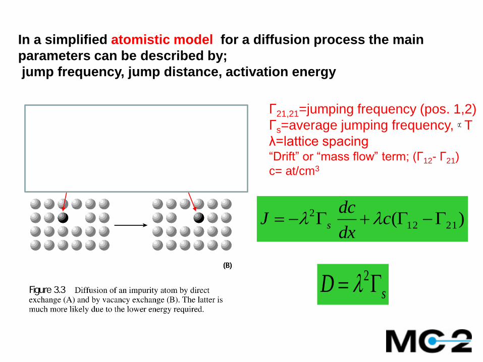
In a simplified atomistic model for a diffusion process the main
parameters can be described by;
jump frequency, jump distance, activation energy
)( 2112
2 cdx
dcJ s
sD 2
Γ21,21=jumping frequency (pos. 1,2)
Γs=average jumping frequency, T
λ=lattice spacing“Drift” or “mass flow” term; (Γ12- Γ21)
c= at/cm3
position1 position2
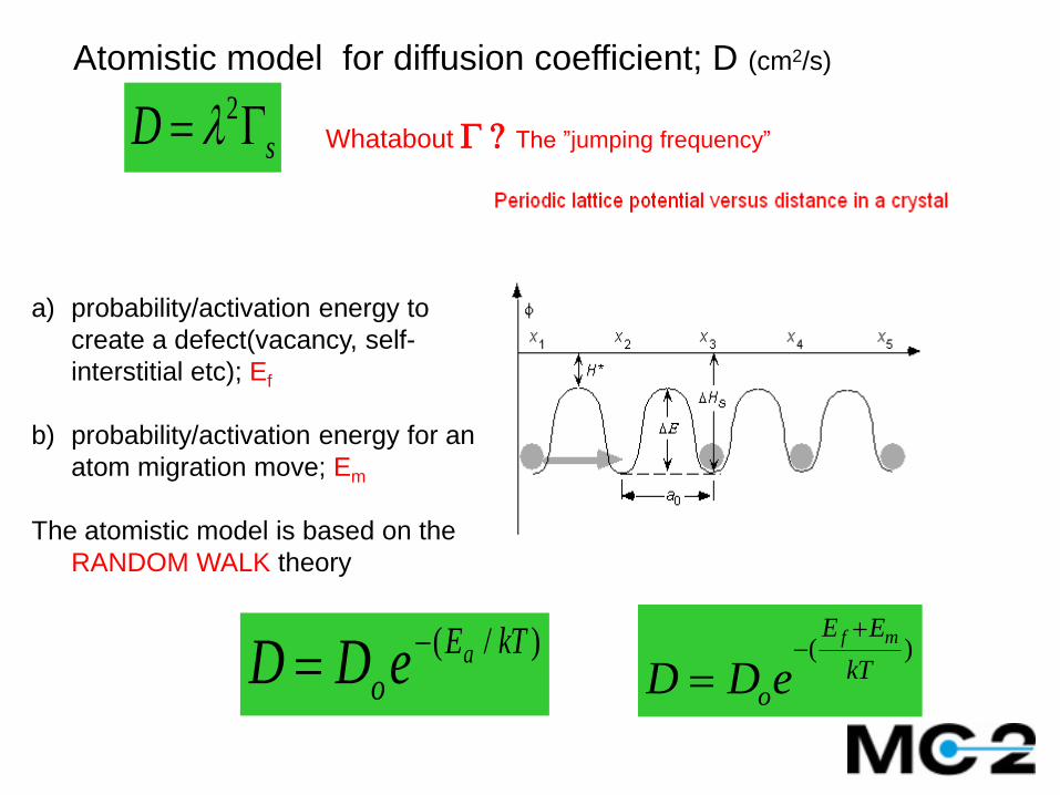
a) probability/activation energy to
create a defect(vacancy, self-
interstitial etc); Ef
b) probability/activation energy for an
atom migration move; Em
The atomistic model is based on the
RANDOM WALK theory
)(kT
EE
o
mf
eDD
)/( kTE
oaeDD
Atomistic model for diffusion coefficient; D (cm2/s)
sD 2 Whatabout ? The ”jumping frequency”
Animations on website! http://www.tf.uni-kiel.de/matwis/amat/def_en/
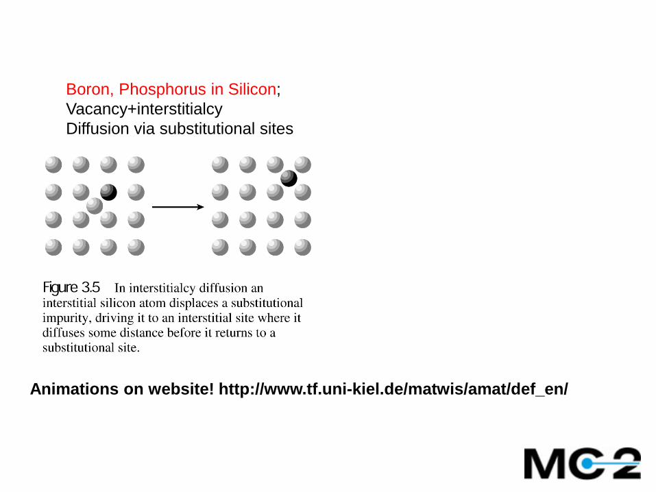
Boron, Phosphorus in Silicon;
Vacancy+interstitialcy
Diffusion via substitutional sites
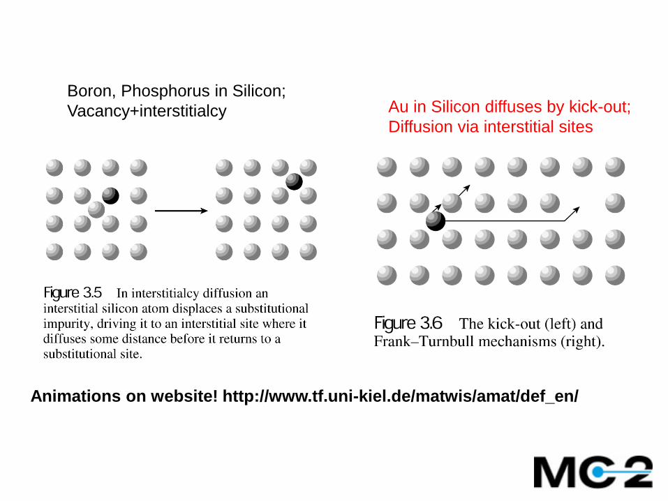
Animations on website! http://www.tf.uni-kiel.de/matwis/amat/def_en/
Au in Silicon diffuses by kick-out;
Diffusion via interstitial sites
Boron, Phosphorus in Silicon;
Vacancy+interstitialcy
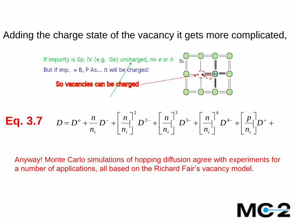
Adding the charge state of the vacancy it gets more complicated,
D
n
pD
n
nD
n
nD
n
nD
n
nDD
iiiii
o 4
4
3
3
2
2
Anyway! Monte Carlo simulations of hopping diffusion agree with experiments for
a number of applications, all based on the Richard Fair’s vacancy model.
Eq. 3.7

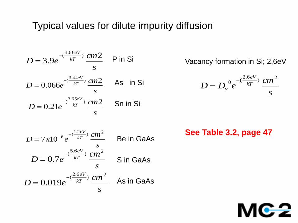
s
cmeD kT
eV2
066.0)
44.3(
s
cmeD kT
eV2
9.3)
66.3(
s
cmeD kT
eV2
21.0)
65.3(
P in Si
As in Si
Sn in Si
Typical values for dilute impurity diffusion
s
cmexD kT
eV 2)
2.1(
6107
s
cmeD kT
eV 2)
6.5(
7.0
s
cmeD kT
eV 2)
6.2(
019.0
Be in GaAs
S in GaAs
As in GaAs
s
cmeDD kT
eV
v
2)
6.2(0
Vacancy formation in Si; 2,6eV
See Table 3.2, page 47
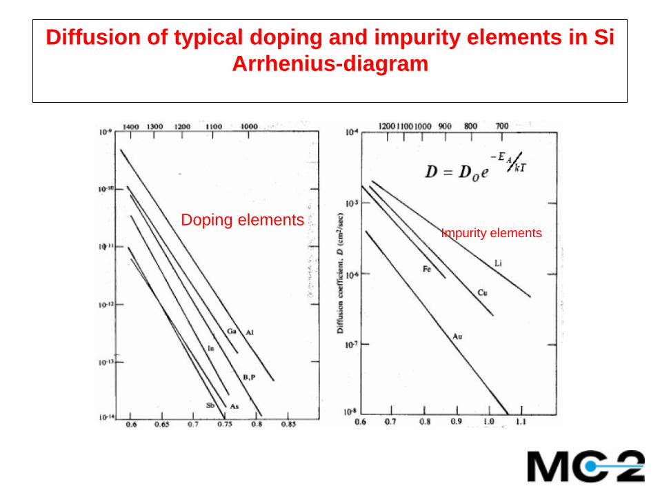
Diffusion of typical doping and impurity elements in Si
Arrhenius-diagram
Doping elementsImpurity elements
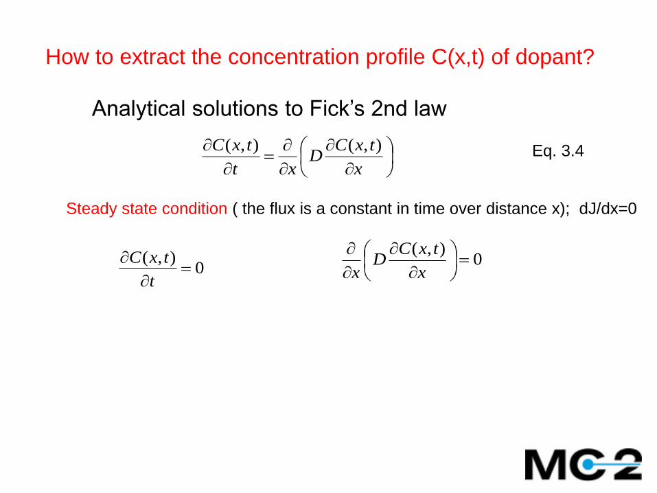
Analytical solutions to Fick’s 2nd law
x
txCD
xt
txC ),(),(
Steady state condition ( the flux is a constant in time over distance x); dJ/dx=0
0),(
t
txC 0),(
x
txCD
x
How to extract the concentration profile C(x,t) of dopant?
Eq. 3.4
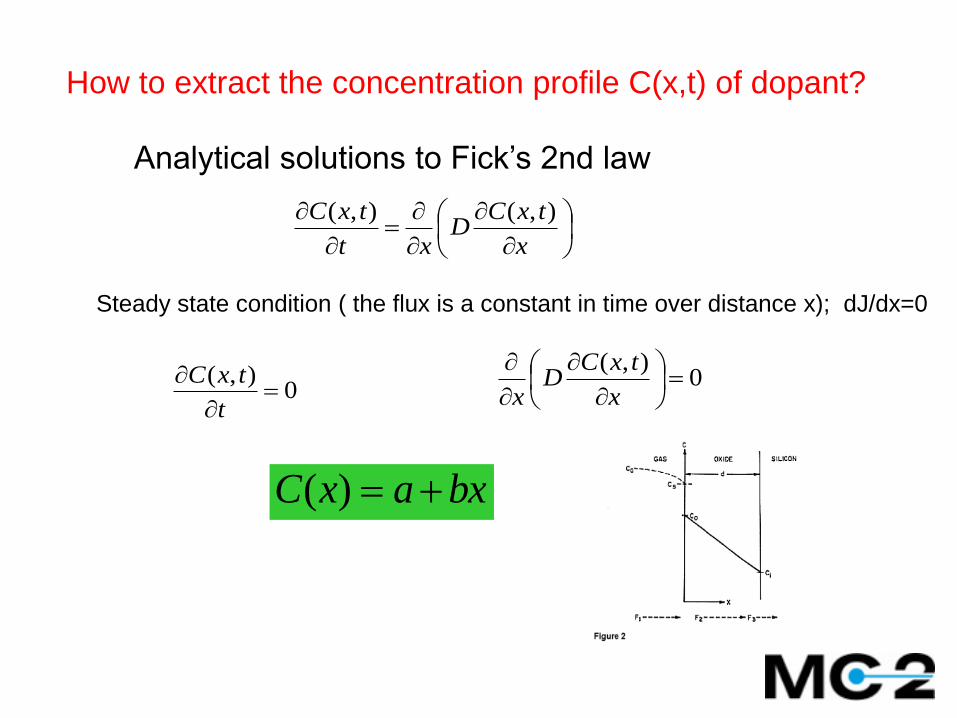
Analytical solutions to Fick’s 2nd law
x
txCD
xt
txC ),(),(
Steady state condition ( the flux is a constant in time over distance x); dJ/dx=0
0),(
t
txC 0),(
x
txCD
x
bxaxC )(
How to extract the concentration profile C(x,t) of dopant?
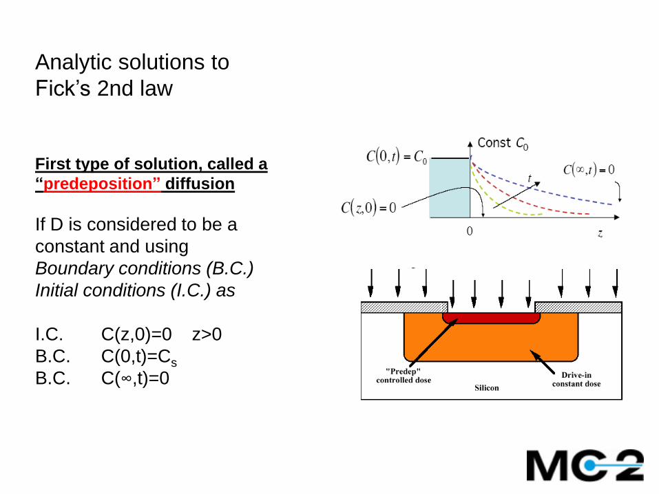
Analytic solutions to
Fick’s 2nd law
First type of solution, called a
“predeposition” diffusion
If D is considered to be a
constant and using
Boundary conditions (B.C.)
Initial conditions (I.C.) as
I.C. C(z,0)=0 z>0
B.C. C(0,t)=Cs
B.C. C(∞,t)=0
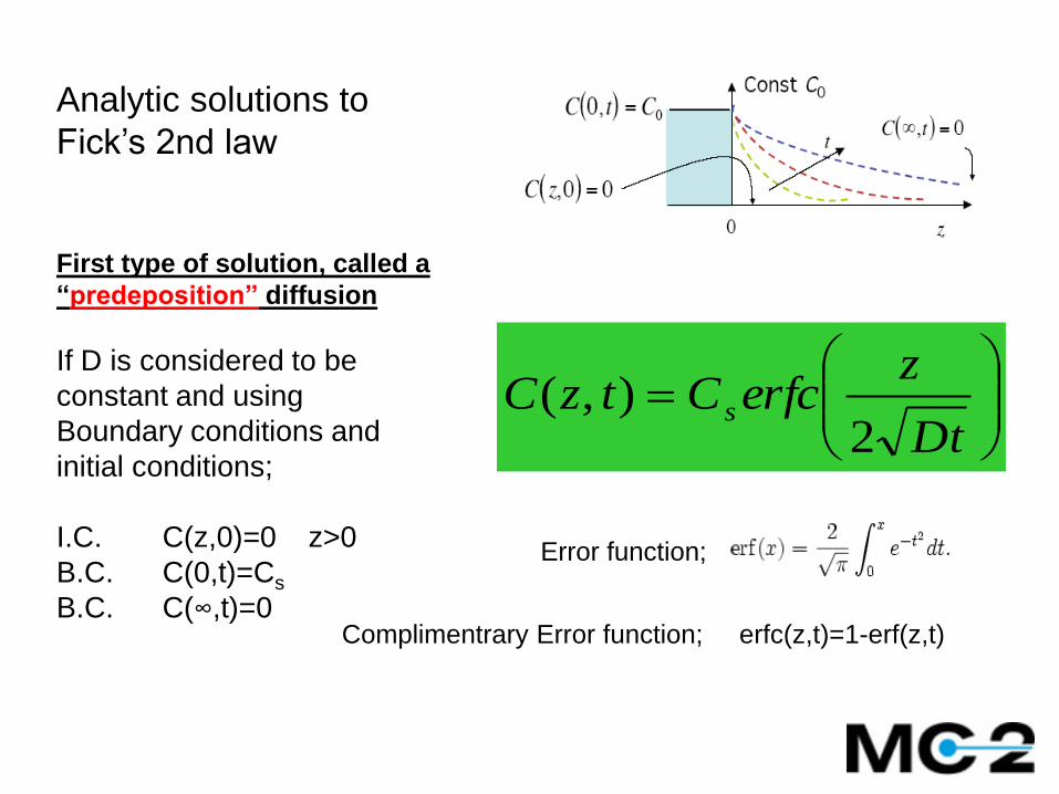
Analytic solutions to
Fick’s 2nd law
First type of solution, called a
“predeposition” diffusion
If D is considered to be
constant and using
Boundary conditions and
initial conditions;
I.C. C(z,0)=0 z>0
B.C. C(0,t)=Cs
B.C. C(∞,t)=0
Dt
zerfcCtzC s
2),(
erfc(z,t)=1-erf(z,t)
Error function;
Complimentrary Error function;
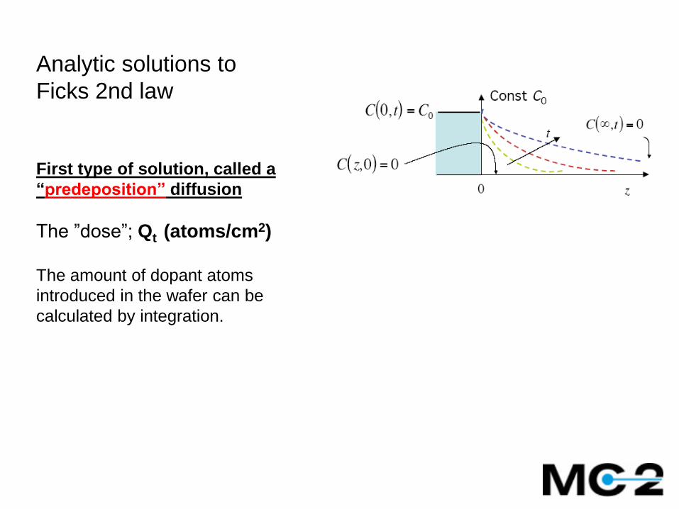
Analytic solutions to
Ficks 2nd law
First type of solution, called a
“predeposition” diffusion
The ”dose”; Qt (atoms/cm2)
The amount of dopant atoms
introduced in the wafer can be
calculated by integration.
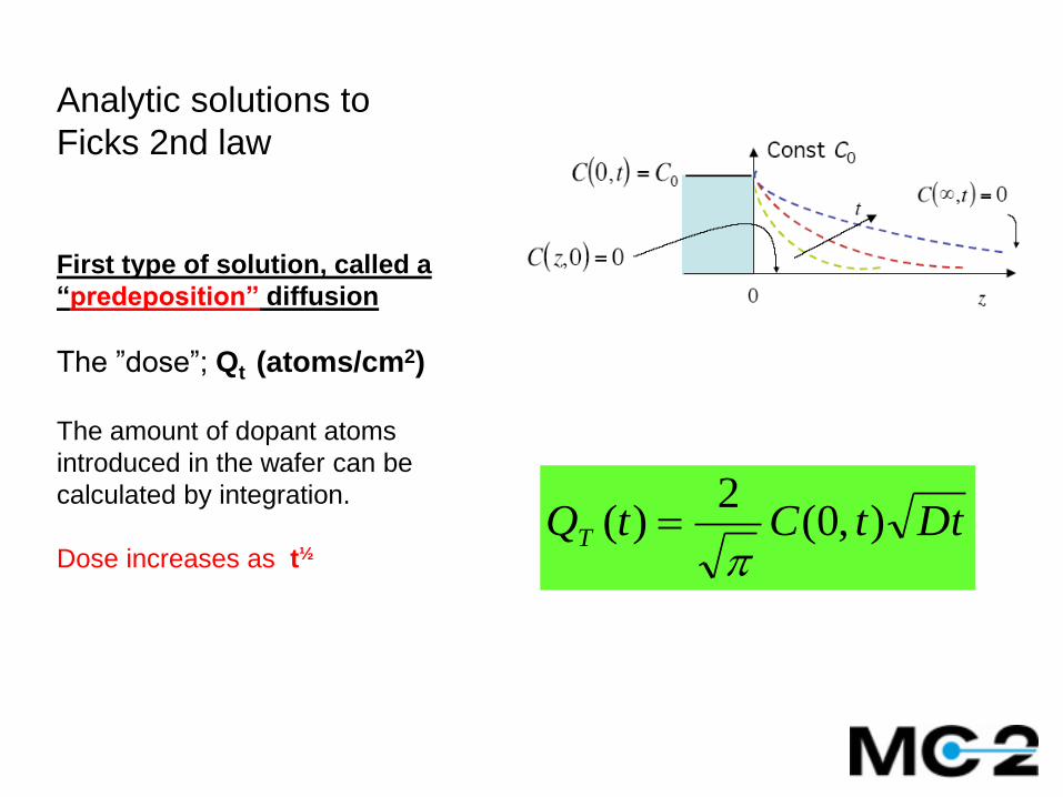
Analytic solutions to
Ficks 2nd law
First type of solution, called a
“predeposition” diffusion
The ”dose”; Qt (atoms/cm2)
The amount of dopant atoms
introduced in the wafer can be
calculated by integration.
Dose increases as t½
DttCtQT ),0(2
)(
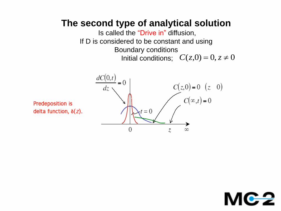
The second type of analytical solutionIs called the “Drive in” diffusion,
If D is considered to be constant and using
Boundary conditions
Initial conditions; 0,0)0,( zzC
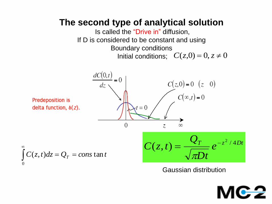
The second type of analytical solutionIs called the “Drive in” diffusion,
If D is considered to be constant and using
Boundary conditions
Initial conditions;
DtzT eDt
QtzC 4/2
),(
0
tan),( tconsQdztzC T
0,0)0,( zzC
Gaussian distribution
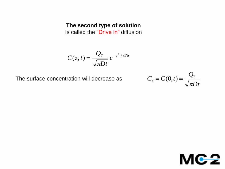
The second type of solution
Is called the “Drive in” diffusion
The surface concentration will decrease as
DtzT eDt
QtzC 4/2
),(
Dt
QtCC T
s
),0(
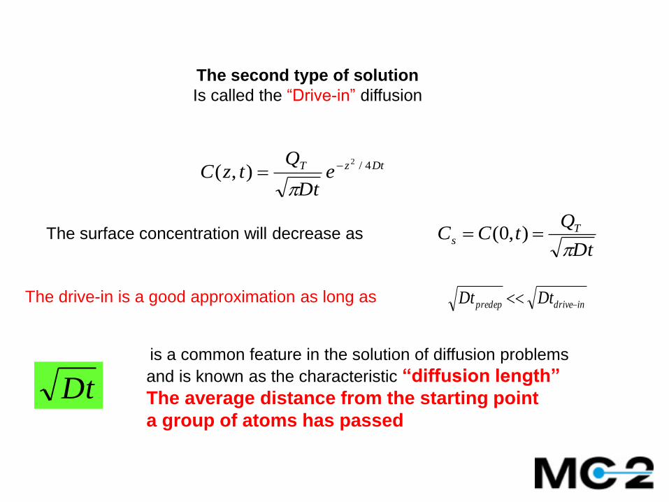
The second type of solution
Is called the “Drive-in” diffusion
The surface concentration will decrease as
DtzT eDt
QtzC 4/2
),(
The drive-in is a good approximation as long as
Dt
is a common feature in the solution of diffusion problems
and is known as the characteristic “diffusion length”
The average distance from the starting point
a group of atoms has passed
Dt
QtCC T
s
),0(
indrivepredep DtDt
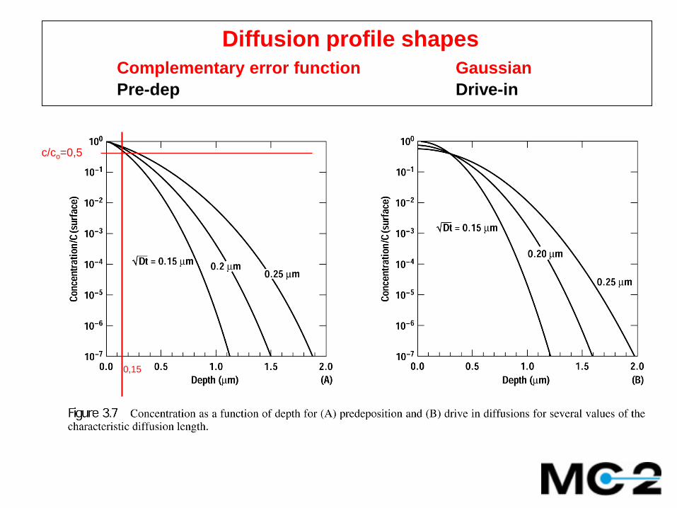
Diffusion profile shapes
Complementary error function Gaussian
Pre-dep Drive-in
0,15
c/co=0,5
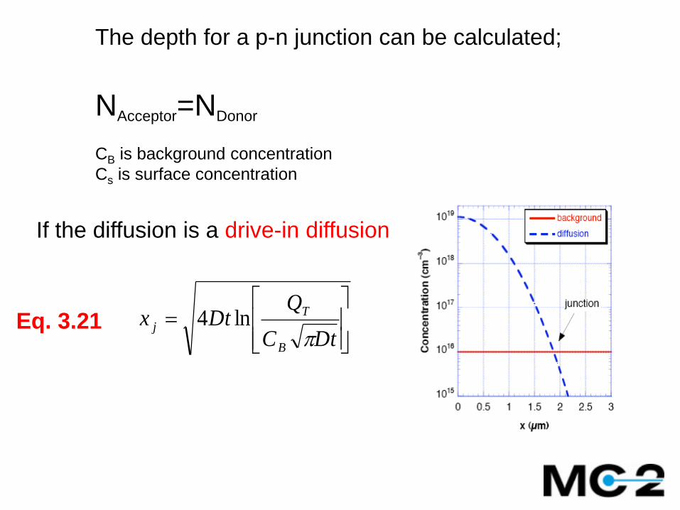
The depth for a p-n junction can be calculated;
NAcceptor=NDonor
CB is background concentration
Cs is surface concentration
DtC
QDtx
B
T
j
ln4
If the diffusion is a drive-in diffusion
Eq. 3.21
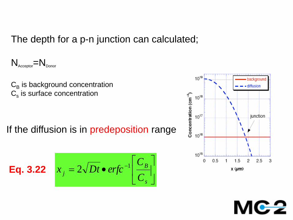
The depth for a p-n junction can calculated;
NAcceptor=NDonor
CB is background concentration
Cs is surface concentration
s
B
jC
CerfcDtx 12
If the diffusion is in predeposition range
Eq. 3.22
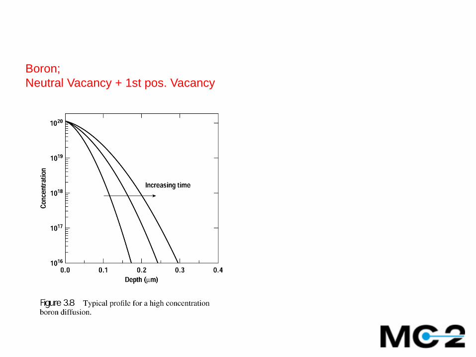
Boron;
Neutral Vacancy + 1st pos. Vacancy
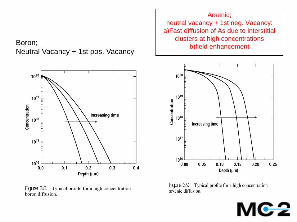
Arsenic;
neutral vacancy + 1st neg. Vacancy:
a)Fast diffusion of As due to interstitial
clusters at high concentrations
b)field enhancementBoron;
Neutral Vacancy + 1st pos. Vacancy
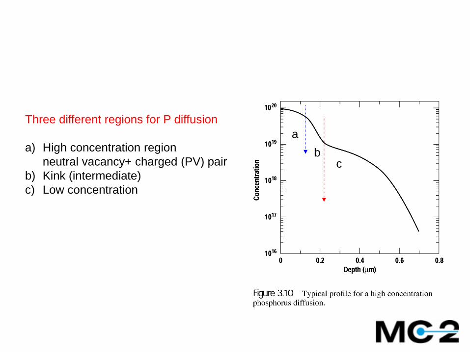
Three different regions for P diffusion
a) High concentration region
neutral vacancy+ charged (PV) pair
b) Kink (intermediate)
c) Low concentration
a
bc
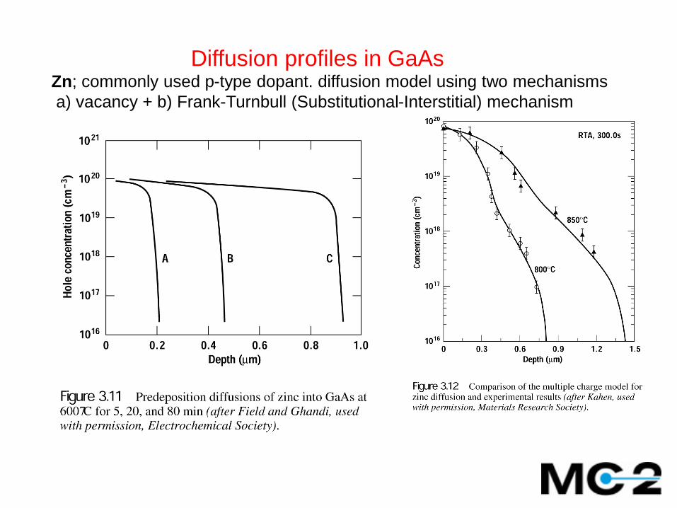
Diffusion profiles in GaAsZn; commonly used p-type dopant. diffusion model using two mechanisms
a) vacancy + b) Frank-Turnbull (Substitutional-Interstitial) mechanism
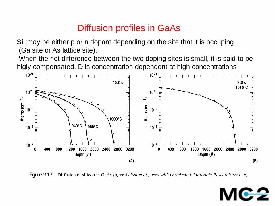
Diffusion profiles in GaAs
Si ;may be either p or n dopant depending on the site that it is occuping
(Ga site or As lattice site).
When the net difference between the two doping sites is small, it is said to be
higly compensated. D is concentration dependent at high concentrations
SUMMARY- DIFFUSION
Statistical and atomistic models
Analytical solutions to Fick’s 2nd law
Pre-dep and drive-in diffusion
Diffusivity depends on ”the circumstances”;
Surface, thin film and bulk etc
Simulation-TCAD-Lecture 3http://www.silvaco.com/products/tcad/process_simulation/at
hena/athenaComparison.html