metasurface holograms for visible light - purdue …shalaev/publication_list...article received 28...
TRANSCRIPT

ARTICLE
Received 28 Apr 2013 | Accepted 23 Oct 2013 | Published 15 Nov 2013
Metasurface holograms for visible lightXingjie Ni1, Alexander V. Kildishev1 & Vladimir M. Shalaev1
Holography, a revolutionary 3D imaging technique, has been developed for storing
and recovering the amplitude and phase of light scattered by objects. Later, single-beam
computer-generated phase holography was proposed for restoring the wavefront from a
given incidence. However, because the phase modulation depends on the light propagation
inside the material, the thickness of phase holograms usually remains comparable to the
wavelength. Here we experimentally demonstrate ultra-thin metasurface holograms that
operate in the visible range whose thickness is only 30 nm (approximately 1/23 of the
operational wavelength). To our knowledge, this is the thinnest hologram that can provide
both amplitude and phase modulation in the visible wavelength range, which generates high-
resolution low-noise images. Using this technique, not only the phase, but potentially the
amplitude of the incident wave can be efficiently controlled, expanding the route to new
applications of ultra-thin and surface-confined photonic devices.
DOI: 10.1038/ncomms3807
1 School of Electrical and Computer Engineering and Birck Nanotechnology Center, Purdue University, West Lafayette, Indiana 47907, USA. Correspondenceand requests for materials should be addressed to V.M.S. (email: [email protected]).
NATURE COMMUNICATIONS | 4:2807 | DOI: 10.1038/ncomms3807 | www.nature.com/naturecommunications 1
& 2013 Macmillan Publishers Limited. All rights reserved.

Traditional two-beam holography relies on recording theinterference pattern of the scattered light and a coherentreference beam1,2. This technique produces an amplitude
hologram through which the scattered wavefront is directlyrecorded through the intensity of the interference pattern. Bytranslating the intensity variations in the interference pattern intophase variations, one may build a phase hologram, whichincreases the brightness of the image substantially3,4. Incontrast to two-beam holography, one of the earliest computer-generated phase holograms, a kinoform5,6, has been designed as acomplex lens which transforms a given incident wavefront intothe transmitted wavefront used to recreate the desired image. Torestore the image, this phase hologram uses a single diffractionorder, which (in the ideal case) includes all of the spatial modes ofthe modulated incident light. This hologram has utilized only thephase of an incident wave, whereas the amplitude of thewavefront in the hologram plane has been assumed constant5,6.The progression of micro- and nano-scale lithographicfabrication has revitalized the area of computer-synthesizedphase holograms through controlling the phase with pixelatedarrays of structural unit cells made of single-layer subwavelength-pitch dielectric gratings7, dielectric optical antennas8 ormultilayer metamaterial media9,10. The computer-generatedapproach to designing these phase holograms has alreadyresulted in sophisticated applications11, which are extremelydifficult to obtain with a fully optical recording process. Becausethe phase modulation in the above phase holograms relies ondielectric optical antennas or the difference of the refractive indexchanges in a transparent layer, the complete phase controlrequires the wavelength-scale or even larger size of unit cells and/or thickness of the phase hologram.
Optical metasurfaces, the basis for our computer-synthesizedand nano-fabricated hologram, have already exhibited unusualphenomena in ways that traditional optical materials, coatingsand devices are unable to duplicate12–24. The field of meta-surfaces is rapidly expanding, and have already been usedto bend light abnormally12,19, rotate polarization25, engineerthe optical spin–orbital interaction23,24, create12,15 or detect20
optical vortex beams, couple propagating waves to surfacewaves17, and create ultra-thin planar lenses18,26–29.
In this article, we experimentally demonstrate an advancedhologram (compare, for example, refs 30,31) recorded as ananostructured plasmonic metasurface32, which directly recordsboth the amplitude and phase of the wavefront scattered by anobject. Similar to the kinoform, our approach requires noreference beam and generates no conjugate image, as all the
spatial bandwidth of the metasurface hologram is utilized in aholographic picture. Furthermore, as the metasurface hologrammodulates both amplitude and phase on a subwavelength scale,the proposed approach can achieve conceptually much higherdiffraction efficiency (the fraction of the transmitted energy of thecross-polarized light that contributes into the holographic image)than traditional holograms as all the orders of diffraction fullycontribute to the holographic image. At the same time ultra-thin,ultra-small holograms can now be recorded, providingunprecedented spatial resolution, low noise, and high precisionof the reconstructed image. Conventionally, a phase hologram ismade by engineering the local optical path by changing eitherthe thickness or the refractive index of a material layer33,34.In ref. 9 a multilayer, graded-index metamaterial has been used todemonstrate a mid-infrared phase hologram, where the requiredphase modulation was provided by local optical paths through astructure with a thickness on the order of the incidentwavelength. In this study, we demonstrate holographic imagesgenerated at a wavelength of 676 nm by a 30-nm thick planarmetasurface hologram, consisting of an array of phase-controllingplasmonic nanoantennas.
ResultsMetasurface hologram design principles. To create the meta-surface hologram, we use a set of the Babinet-inverted, com-plementary nanoantennas (CNAs)—nano-voids of differentshapes perforated in a thin, metallic film on a glass substrate.Each CNA shape provides a specific phase shift to thecross-polarized, scattered light (that is, the scattered polarizationis perpendicular to the incident polarization, see Methodssection). As the CNAs scatter both co-polarized andcross-polarized light, we cannot totally eliminate the co-polarizedcomponent. However, the complementary design efficiently pre-vents the direct transmission of the co-polarized component asthe rest of the sample remains opaque owing to the continuousmetallic film.
To design the metasurface hologram, we first choose an imageplane and selected a virtual object to be generated in that plane.We have taken the word ‘PURDUE’ as our test virtual object.Next, we consider the test object to emit 676-nm linearlypolarized coherent light, and we mapped the phase and amplitudeof the electric field onto the metasurface hologram plane (whichwas taken 10 mm below and parallel to the image plane). A moredetailed explanation of the constructing procedure can be foundin the Methods section. Figure 1a illustrates this design step by
x (μm)
y (μ
m)
–8 –4 0 4 8
–8
–4
0
4
8
Nor
mal
ized
am
plitu
de
x (μm)
y (μm)0
0.25π
0.5π
0.75π
π
1.25π
1.5π
1.75π
2π
0
0.25π
0.5π
0.75π
π
1.25π
1.5π
1.75π
2π
1010 μm
0Im
age plane
Metasurfa
ce
0.5
1
50
–5–10 –10
–50
510
Figure 1 | Metasurface hologram design steps. (a) An image plane is chosen above the metasurface hologram at a given distance (here we choose
10mm). A flat, light-emitting virtual object is located in the image plane. The phase and amplitude distribution of the electric field propagating from the
object are mapped to the metasurface plane. (b) The calculated amplitude (z value) and phase distribution (pseudo-colour map) on the metasurface
plane. (c) The discrete eight-level phase distribution with a two-level amplitude modulation to accommodate the antenna designs. The blank areas indicate
the ‘off’ state and also correspond to ‘blank’ pixels.
ARTICLE NATURE COMMUNICATIONS | DOI: 10.1038/ncomms3807
2 NATURE COMMUNICATIONS | 4:2807 | DOI: 10.1038/ncomms3807 | www.nature.com/naturecommunications
& 2013 Macmillan Publishers Limited. All rights reserved.
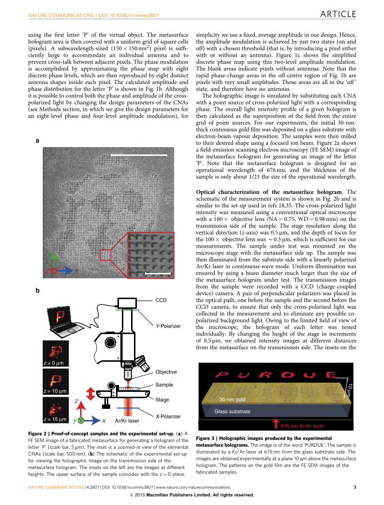
using the first letter ‘P’ of the virtual object. The metasurfacehologram area is then covered with a uniform grid of square cells(pixels). A subwavelength-sized (150� 150 nm2) pixel is suffi-ciently large to accommodate an individual antenna and toprevent cross-talk between adjacent pixels. The phase modulationis accomplished by approximating the phase map with eightdiscrete phase levels, which are then reproduced by eight distinctantenna shapes inside each pixel. The calculated amplitude andphase distribution for the letter ‘P’ is shown in Fig. 1b. Althoughit is possible to control both the phase and amplitude of the cross-polarized light by changing the design parameters of the CNAs(see Methods section, in which we give the design parameters foran eight-level phase and four-level amplitude modulation), for
simplicity we use a fixed, average amplitude in our design. Hence,the amplitude modulation is achieved by just two states (on andoff) with a chosen threshold (that is, by introducing a pixel eitherwith or without an antenna). Figure 1c shows the simplifieddiscrete phase map using this two-level amplitude modulation.The blank areas indicate pixels without antennas. Note that therapid phase-change areas in the off-centre region of Fig. 1b arepixels with very small amplitudes. Those areas are all in the ‘off ’state, and therefore have no antennas.
The holographic image is simulated by substituting each CNAwith a point source of cross-polarized light with a correspondingphase. The overall light intensity profile of a given hologram isthen calculated as the superposition of the field from the entiregrid of point sources. For our experiments, the initial 30-nm-thick continuous gold film was deposited on a glass substrate withelectron-beam vapour deposition. The samples were then milledto their desired shape using a focused ion beam. Figure 2a showsa field-emission scanning electron microscopy (FE SEM) image ofthe metasurface hologram for generating an image of the letter‘P’. Note that the metasurface hologram is designed for anoperational wavelength of 676 nm, and the thickness of thesample is only about 1/23 the size of the operational wavelength.
Optical characterization of the metasurface hologram. Theschematic of the measurement system is shown in Fig. 2b and issimilar to the set-up used in refs 18,35. The cross-polarized lightintensity was measured using a conventional optical microscopewith a 100� objective lens (NA¼ 0.75, WD¼ 0.98 mm) on thetransmission side of the sample. The stage resolution along thevertical direction (z-axis) was 0.5 mm, and the depth of focus forthe 100� objective lens was B0.5 mm, which is sufficient for ourmeasurements. The sample under test was mounted on themicroscope stage with the metasurface side up. The sample wasthen illuminated from the substrate side with a linearly polarizedAr/Kr laser in continuous-wave mode. Uniform illumination wasensured by using a beam diameter much larger than the size ofthe metasurface hologram under test. The transmission imagesfrom the sample were recorded with a CCD (charge-coupleddevice) camera. A pair of perpendicular polarizers was placed inthe optical path, one before the sample and the second before theCCD camera, to ensure that only the cross-polarized light wascollected in the measurement and to eliminate any possible co-polarized background light. Owing to the limited field of view ofthe microscope, the hologram of each letter was testedindividually. By changing the height of the stage in incrementsof 0.5 mm, we obtained intensity images at different distancesfrom the metasurface on the transmission side. The insets on the
CCD
a
Y-Polarizer
Objective
Stage
Sample
X-Polarizer
100X
Ar/Kr laserx
z
y
50Xz = 0 μm
z = 10 μm
z = 15 μm
xz
y
b
Figure 2 | Proof-of-concept samples and the experimental set-up. (a) A
FE SEM image of a fabricated metasurface for generating a hologram of the
letter ‘P’ (scale bar, 5 mm). The inset is a zoomed-in view of the elemental
CNAs (scale bar, 500 nm). (b) The schematic of the experimental set-up
for viewing the holographic image on the transmission side of the
metasurface hologram. The insets on the left are the images at different
heights. The upper surface of the sample coincides with the z¼0 plane.
676-nm Kr/Ar laser
Glass substrate
30-nm gold
10 μm
Figure 3 | Holographic images produced by the experimental
metasurface holograms. The image is of the word ‘PURDUE’. The sample is
illuminated by a Kr/Ar laser at 676 nm from the glass substrate side. The
images are obtained experimentally at a plane 10mm above the metasurface
hologram. The patterns on the gold film are the FE SEM images of the
fabricated samples.
NATURE COMMUNICATIONS | DOI: 10.1038/ncomms3807 ARTICLE
NATURE COMMUNICATIONS | 4:2807 | DOI: 10.1038/ncomms3807 | www.nature.com/naturecommunications 3
& 2013 Macmillan Publishers Limited. All rights reserved.

left of Fig. 2b are the images obtained at different heights. Thelight focuses at a height of 10mm forming a clear image of letter‘P’ as designed.
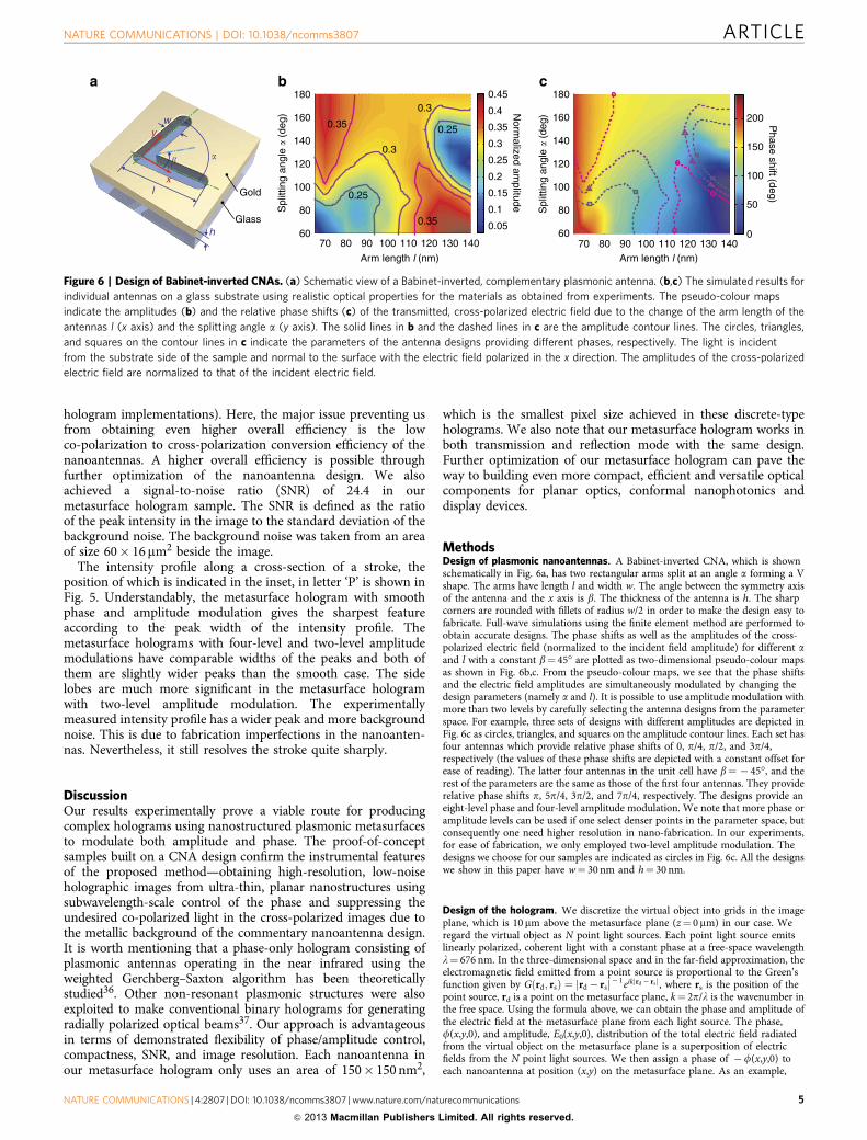
Figure 3 illustrates the entire sample structure and theholographic images formed above the sample. The patterns onthe gold films are the SEM images of the metasurface hologramsamples. The images ‘floating’ above the sample are the actuallight intensity maps obtained from the optical experiment.Figure 4a shows the holographic images simulated with an idealpixelated metasurface hologram using the exact phase andamplitude modulations inside each pixel. In this scenario, theoriginal object is restored almost perfectly. Figure 4b shows thesimulated holographic images created by the metasurfacehologram using the approximate eight-level phase and four-levelamplitude modulations. Figure 4c shows the simulated holo-graphic images created by the metasurface hologram using theapproximate eight-level phase and two-level amplitude modula-tions. Figure 4d depicts the images obtained from our experi-ments. Although there are two more levels for the amplitudemodulation in Fig. 4c compared with Fig. 4b, the qualityimprovement is limited. The noticeable effect is that thebackground noise is reduced when more amplitude levels areused, which might be important for more complex holographicimages. In our case, two-level amplitude modulation is sufficientfor producing clear images. All the images were taken at the sameimage plane, 10mm above and parallel to the metasurfacehologram. The dimensions of the individual letters obtainedfrom the experiment are o8� 8 mm2, whereas the dimensions ofthe corresponding metasurface hologram patch for each letter areonly about 1.5 times larger (o12� 12 mm2). The width of thestroke of each letter is B1 mm.
This proof-of-concept design works at a visible wavelengthof 676 nm, and the experimental images match the simulatedresults. Supplementary Movies 1 and 2 demonstrate theevolution of the images taken at different elevationsabove the metasurface hologram for both simulated andexperimental data.
Quantitative analysis. An overall efficiency of B10% (the frac-tion of the incident energy that contributes into the transmittedholographic image) is achieved in our metasurface hologramdesign, which is about one order of magnitude greater than theexisting metamaterial holograms9,10. We note that there is noenergy going to higher order diffraction (in contrast to the typical
Intensity (a.u.)
8
4
0
–4
y (μ
m)
y (μ
m)
y (μ
m)
y (μ
m)
–88
4
0
–4
–88
4
0
–4
–88
4
0
–4
–8–48 –40 –32 –24 –16 –8 0
x (μm)8 16 24 32 40 48
0
0.1
0.2
0.3
0.4
0.5
0.6
0.7
0.8
0.9
1
Figure 4 | Simulated holographic images compared with the experimental images. (a) The simulated holographic images created by an ideal
metasurface hologram with smooth phase and amplitude modulations. (b) The simulated holographic images created by a metasurface hologram with an
eight-level phase modulation and a four-level amplitude modulation. (c) The simulated holographic images created by a metasurface hologram with an
eight-level phase modulation and a two-level amplitude modulation. (d) Holographic images obtained experimentally from the fabricated samples.
All the images are taken from the same image plane 10 mm above and parallel to the metasurface hologram.
2.5 3 3.5 4 4.5 50
0.2
0.4
0.6
0.8
1
y position [μm]
Nor
mal
ized
inte
nsity
–4 0 4
–4
0
4
x [μm]
y [μ
m]
Ideal4AM, 8PM2AM, 8PMExperiment
Figure 5 | Normalized intensity profiles of a cross-section of a stroke in
the letter ‘P’. The dashed line is the simulated result from an ideal
metasurface hologram with smooth phase and amplitude modulations. The
dash-dotted line is the simulated result from a metasurface hologram with
an eight-level phase modulation (8PM) and a four-level amplitude
modulation (4AM). The dotted line shows the simulated result for a
metasurface hologram with an eight-level phase modulation (8PM) and a
two-level amplitude modulation (2AM). The solid line is the measured
result from the fabricated sample. The dashed line in the inset indicates the
position where the cross-section is taken.
ARTICLE NATURE COMMUNICATIONS | DOI: 10.1038/ncomms3807
4 NATURE COMMUNICATIONS | 4:2807 | DOI: 10.1038/ncomms3807 | www.nature.com/naturecommunications
& 2013 Macmillan Publishers Limited. All rights reserved.
hologram implementations). Here, the major issue preventing usfrom obtaining even higher overall efficiency is the lowco-polarization to cross-polarization conversion efficiency of thenanoantennas. A higher overall efficiency is possible throughfurther optimization of the nanoantenna design. We alsoachieved a signal-to-noise ratio (SNR) of 24.4 in ourmetasurface hologram sample. The SNR is defined as the ratioof the peak intensity in the image to the standard deviation of thebackground noise. The background noise was taken from an areaof size 60� 16mm2 beside the image.
The intensity profile along a cross-section of a stroke, theposition of which is indicated in the inset, in letter ‘P’ is shown inFig. 5. Understandably, the metasurface hologram with smoothphase and amplitude modulation gives the sharpest featureaccording to the peak width of the intensity profile. Themetasurface holograms with four-level and two-level amplitudemodulations have comparable widths of the peaks and both ofthem are slightly wider peaks than the smooth case. The sidelobes are much more significant in the metasurface hologramwith two-level amplitude modulation. The experimentallymeasured intensity profile has a wider peak and more backgroundnoise. This is due to fabrication imperfections in the nanoanten-nas. Nevertheless, it still resolves the stroke quite sharply.
DiscussionOur results experimentally prove a viable route for producingcomplex holograms using nanostructured plasmonic metasurfacesto modulate both amplitude and phase. The proof-of-conceptsamples built on a CNA design confirm the instrumental featuresof the proposed method—obtaining high-resolution, low-noiseholographic images from ultra-thin, planar nanostructures usingsubwavelength-scale control of the phase and suppressing theundesired co-polarized light in the cross-polarized images due tothe metallic background of the commentary nanoantenna design.It is worth mentioning that a phase-only hologram consisting ofplasmonic antennas operating in the near infrared using theweighted Gerchberg–Saxton algorithm has been theoreticallystudied36. Other non-resonant plasmonic structures were alsoexploited to make conventional binary holograms for generatingradially polarized optical beams37. Our approach is advantageousin terms of demonstrated flexibility of phase/amplitude control,compactness, SNR, and image resolution. Each nanoantenna inour metasurface hologram only uses an area of 150� 150 nm2,
which is the smallest pixel size achieved in these discrete-typeholograms. We also note that our metasurface hologram works inboth transmission and reflection mode with the same design.Further optimization of our metasurface hologram can pave theway to building even more compact, efficient and versatile opticalcomponents for planar optics, conformal nanophotonics anddisplay devices.
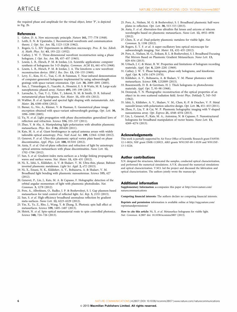
MethodsDesign of plasmonic nanoantennas. A Babinet-inverted CNA, which is shownschematically in Fig. 6a, has two rectangular arms split at an angle a forming a Vshape. The arms have length l and width w. The angle between the symmetry axisof the antenna and the x axis is b. The thickness of the antenna is h. The sharpcorners are rounded with fillets of radius w/2 in order to make the design easy tofabricate. Full-wave simulations using the finite element method are performed toobtain accurate designs. The phase shifts as well as the amplitudes of the cross-polarized electric field (normalized to the incident field amplitude) for different aand l with a constant b¼ 45� are plotted as two-dimensional pseudo-colour mapsas shown in Fig. 6b,c. From the pseudo-colour maps, we see that the phase shiftsand the electric field amplitudes are simultaneously modulated by changing thedesign parameters (namely a and l). It is possible to use amplitude modulation withmore than two levels by carefully selecting the antenna designs from the parameterspace. For example, three sets of designs with different amplitudes are depicted inFig. 6c as circles, triangles, and squares on the amplitude contour lines. Each set hasfour antennas which provide relative phase shifts of 0, p/4, p/2, and 3p/4,respectively (the values of these phase shifts are depicted with a constant offset forease of reading). The latter four antennas in the unit cell have b¼ � 45�, and therest of the parameters are the same as those of the first four antennas. They providerelative phase shifts p, 5p/4, 3p/2, and 7p/4, respectively. The designs provide aneight-level phase and four-level amplitude modulation. We note that more phase oramplitude levels can be used if one select denser points in the parameter space, butconsequently one need higher resolution in nano-fabrication. In our experiments,for ease of fabrication, we only employed two-level amplitude modulation. Thedesigns we choose for our samples are indicated as circles in Fig. 6c. All the designswe show in this paper have w¼ 30 nm and h¼ 30 nm.
Design of the hologram. We discretize the virtual object into grids in the imageplane, which is 10 mm above the metasurface plane (z¼ 0 mm) in our case. Weregard the virtual object as N point light sources. Each point light source emitslinearly polarized, coherent light with a constant phase at a free-space wavelengthl¼ 676 nm. In the three-dimensional space and in the far-field approximation, theelectromagnetic field emitted from a point source is proportional to the Green’sfunction given by Gðrd; rsÞ ¼ rd � rsj j� 1eik rd � rsj j , where rs is the position of thepoint source, rd is a point on the metasurface plane, k¼ 2p/l is the wavenumber inthe free space. Using the formula above, we can obtain the phase and amplitude ofthe electric field at the metasurface plane from each light source. The phase,f(x,y,0), and amplitude, E0(x,y,0), distribution of the total electric field radiatedfrom the virtual object on the metasurface plane is a superposition of electricfields from the N point light sources. We then assign a phase of �f(x,y,0) toeach nanoantenna at position (x,y) on the metasurface plane. As an example,
70 80 90 100 110 120 130 14060
80
100
120
140
160
180
Spl
ittin
g an
gle
� (d
eg) N
ormalized am
plitude
0.05
0.1
0.15
0.2
0.25
0.3
0.35
0.4
0.45
70 80 90 100 110 120 130 14060
80
100
120
140
160
180
Spl
ittin
g an
gle
� (d
eg)
Phase shift (deg)
0
50
100
150
200
cb
h
w
lx
y
Gold
Glass
a
0.25
0.250.35
0.35
0.3
0.3
� �
Arm length l (nm) Arm length l (nm)
Figure 6 | Design of Babinet-inverted CNAs. (a) Schematic view of a Babinet-inverted, complementary plasmonic antenna. (b,c) The simulated results for
individual antennas on a glass substrate using realistic optical properties for the materials as obtained from experiments. The pseudo-colour maps
indicate the amplitudes (b) and the relative phase shifts (c) of the transmitted, cross-polarized electric field due to the change of the arm length of the
antennas l (x axis) and the splitting angle a (y axis). The solid lines in b and the dashed lines in c are the amplitude contour lines. The circles, triangles,
and squares on the contour lines in c indicate the parameters of the antenna designs providing different phases, respectively. The light is incident
from the substrate side of the sample and normal to the surface with the electric field polarized in the x direction. The amplitudes of the cross-polarized
electric field are normalized to that of the incident electric field.
NATURE COMMUNICATIONS | DOI: 10.1038/ncomms3807 ARTICLE
NATURE COMMUNICATIONS | 4:2807 | DOI: 10.1038/ncomms3807 | www.nature.com/naturecommunications 5
& 2013 Macmillan Publishers Limited. All rights reserved.
the required phase and amplitude for the virtual object, letter ‘P’, is depictedin Fig. 2b.
References1. Gabor, D. A. New microscopic principle. Nature 161, 777–778 (1948).2. Leith, E. N. & Upatnieks, J. Reconstructed wavefronts and communication
theory. J. Opt. Soc. Am. 52, 1123–1128 (1962).3. Rogers, G. L. XIV Experiments in diffraction microscopy. Proc. R. Soc. Edinb.
A. Math. Phys. Sci. 63, 193–221 (1952).4. Cathey, J. W. T. Three-dimensional wavefront reconstruction using a phase
hologram. J. Opt. Soc. Am. 55, 457–457 (1965).5. Lesem, L. B., Hirsch, P. M. & Jordan, J.A. Scientific applications: computer
synthesis of holograms for 3-D display. Commun. ACM 11, 661–674 (1968).6. Lesem, L. B., Hirsch, P. M. & Jordan, J. A. The kinoform: a new wavefront
reconstruction device. IBM J. Res. Dev. 13, 150–155 (1969).7. Levy, U., Kim, H.-C., Tsai, C.-H. & Fainman, Y. Near-infrared demonstration
of computer-generated holograms implemented by using subwavelengthgratings with space-variant orientation. Opt. Lett. 30, 2089–2091 (2005).
8. Sun, J., Timurdogan, E., Yaacobi, A., Hosseini, E. S. & Watts, M. R. Large-scalenanophotonic phased array. Nature 493, 195–199 (2013).
9. Larouche, S., Tsai, Y.-J., Tyler, T., Jokerst, N. M. & Smith, D. R. Infraredmetamaterial phase holograms. Nat. Mater. 11, 450–454 (2012).
10. Walther, B. et al. Spatial and spectral light shaping with metamaterials. Adv.Mater. 24, 6300–6304 (2012).
11. Biener, G., Niv, A., Kleiner, V. & Hasman, E. Geometrical phase imageencryption obtained with space-variant subwavelength gratings. Opt. Lett. 30,1096–1098 (2005).
12. Yu, N. et al. Light propagation with phase discontinuities: generalized laws ofreflection and refraction. Science 334, 333–337 (2011).
13. Zhao, Y. & Alu, A. Manipulating light polarization with ultrathin plasmonicmetasurfaces. Phys. Rev. B 84, 205428 (2011).
14. Kats, M. A. et al. Giant birefringence in optical antenna arrays with widelytailorable optical anisotropy. Proc. Natl Acad. Sci. 109, 12364–12368 (2012).
15. Genevet, P. et al. Ultra-thin plasmonic optical vortex plate based on phasediscontinuities. Appl. Phys. Lett. 100, 013101 (2012).
16. Aieta, F. et al. Out-of-plane reflection and refraction of light by anisotropicoptical antenna metasurfaces with phase discontinuities. Nano Lett. 12,1702–1706 (2012).
17. Sun, S. et al. Gradient-index meta-surfaces as a bridge linking propagatingwaves and surface waves. Nat. Mater. 11, 426–431 (2012).
18. Ni, X., Ishii, S., Kildishev, A. V. & Shalaev, V. M. Ultra-thin, planar, Babinet-inverted plasmonic metalenses. Light Sci. Appl. 2, e72 (2013).
19. Ni, X., Emani, N. K., Kildishev, A. V., Boltasseva, A. & Shalaev, V. M.Broadband light bending with plasmonic nanoantennas. Science 335, 427(2012).
20. Genevet, P., Lin, J., Kats, M. A. & Capasso, F. Holographic detection of theorbital angular momentum of light with plasmonic photodiodes. Nat.Commun. 3, 1278 (2012).
21. Pors, A., Albrektsen, O., Radko, I. P. & Bozhevolnyi, S. I. Gap plasmon-basedmetasurfaces for total control of reflected light. Sci. Rep. 3, 2155 (2013).
22. Sun, S. et al. High-efficiency broadband anomalous reflection by gradientmeta-surfaces. Nano Lett. 12, 6223–6229 (2012).
23. Yin, X., Ye, Z., Rho, J., Wang, Y. & Zhang, X. Photonic spin hall effect atmetasurfaces. Science 339, 1405–1407 (2013).
24. Shitrit, N. et al. Spin-optical metamaterial route to spin-controlled photonics.Science 340, 724–726 (2013).
25. Pors, A., Nielsen, M. G. & Bozhevolnyi, S. I. Broadband plasmonic half-waveplates in reflection. Opt. Lett. 38, 513–515 (2013).
26. Aieta, F. et al. Aberration-free ultrathin flat lenses and axicons at telecomwavelengths based on plasmonic metasurfaces. Nano Lett. 12, 4932–4936(2012).
27. Chen, X. et al. Dual-polarity plasmonic metalens for visible light. Nat.Commun. 3, 1198 (2012).
28. Rogers, E. T. F. et al. A super-oscillatory lens optical microscope forsubwavelength imaging. Nat. Mater. 11, 432–435 (2012).
29. Pors, A., Nielsen, M. G., Eriksen, R. L. & Bozhevolnyi, S. I. Broadband FocusingFlat Mirrors Based on Plasmonic Gradient Metasurfaces. Nano Lett. 13,829–834 (2013).
30. Urbach, J. C. & Meier, R. W. Properties and limitations of hologram recordingmaterials. Appl. Opt. 8, 2269–2281 (1969).
31. Cathey, J. W. T. Phase holograms, phase-only holograms, and kinoforms.Appl. Opt. 9, 1478–1479 (1970).
32. Kildishev, A. V., Boltasseva, A. & Shalaev, V. M. Planar photonics withmetasurfaces. Science 339, 1232009 (2013).
33. Bosomworth, D. R. & Gerritsen, H. J. Thick holograms in photochromicmaterials. Appl. Opt. 7, 95–98 (1968).
34. Denisyuk, Y. N. Photographic reconstruction of the optical properties of anobject in its own scattered radiation field. Soviet Phys. Doklady 7, 543–545(1962).
35. Ishii, S., Kildishev, A. V., Shalaev, V. M., Chen, K.-P. & Drachev, V. P. Metalnanoslit lenses with polarization-selective design. Opt. Lett. 36, 451–453 (2011).
36. Zhou, F., Liu, Y. & Cai, W. P. Plasmonic holographic imaging with V-shapednanoantenna array. Opt. Express 21, 4348–4354 (2013).
37. Lin, J., Genevet, P., Kats, M. A., Antoniou, N. & Capasso, F. Nanostructuredholograms for broadband manipulation of vector beams. Nano Lett. 13,4269–4274 (2013).
AcknowledgementsThis work is partially supported by Air Force Office of Scientific Research grant FA9550-12-1-0024, NSF grant DMR-1120923, ARO grants W911NF-09-1-0539 and W911NF-13-1-0226.
Author contributionsX.N. designed the structures, fabricated the samples, conducted optical characterization,and performed the numerical simulations. A.V.K. discussed the numerical simulationsand optical characterization. V.M.S. led the project and discussed the fabrication andoptical characterization. The authors jointly wrote the manuscript.
Additional informationSupplementary Information accompanies this paper at http://www.nature.com/naturecommunications
Competing financial interests: The authors declare no competing financial interests.
Reprints and permission information is available online at http://npg.nature.com/reprintsandpermissions/
How to cite this article: Ni, X. et al. Metasurface holograms for visible light.Nat. Commun. 4:2807 doi: 10.1038/ncomms3807 (2013).
ARTICLE NATURE COMMUNICATIONS | DOI: 10.1038/ncomms3807
6 NATURE COMMUNICATIONS | 4:2807 | DOI: 10.1038/ncomms3807 | www.nature.com/naturecommunications
& 2013 Macmillan Publishers Limited. All rights reserved.