mechanisms of creep deformation in pure sn solder joints
TRANSCRIPT
Mechanisms of Creep Deformation in Pure Sn Solder Joints
K.-O. LEE,1,2,4 J.W. MORRIS JR.,1 and FAY HUA3
1.—Department of Materials Science and Engineering, University of California, Berkeley,CA 94720, USA. 2.—Now at Intel Corporation, Chandler, AZ 85226, USA. 3.—Intel Corporation,Sunnyvale, CA 95054, USA. 4.—e-mail: [email protected]
The work reported here concerns the creep of pure Sn solder joints with Cumetallization (Cu||Sn||Cu). Steady-state creep tests in shear are combinedwith electron backscatter diffraction (EBSD) analysis of the evolution of themicrostructure during creep to clarify the deformation mechanism and thenature of the microstructural evolution. The creep behavior of the jointchanges significantly with temperature. At low temperature (65�C), two dis-tinct creep mechanisms are observed. Low-stress creep is apparently domi-nated by grain boundary sliding, as evidenced by the low stress exponent(n � 4), low activation energy (Q � 42 kJ/mole), and significant grain rotationduring creep. High-stress creep is dominated by bulk deformation processes,evidenced by a high stress exponent (n � 9), an activation energy like that forbulk diffusion (Q � 70 kJ/mole), and a relatively fixed microstructure. At hightemperature all aspects of its behavior are consistent with deformation bybulk creep mechanisms; the stress exponent and activation energy are high(n � 5 to 7, Q � 96 kJ/mole), and despite significant grain coarsening, themicrostructure retains (and strengthens) a fixed [001] texture. The resultssuggest that a ‘‘segmented’’ constitutive equation of Dorn type is most suitablefor the low-temperature behavior, while a ‘‘hyperbolic’’ constitutive equationmay be preferable at high temperature.
Key words: Tin, creep mechanism, Pb-free solder
INTRODUCTION
The mechanical properties and, hence, the reli-ability of a solder joint depend strongly on itsmicrostructure, which evolves under the influenceof temperature and stress during service. In lead–tin solders with two-phase microstructures thecoarsening of the eutectic lamellar structure withtemperature and stress is apparent on metallo-graphic examination, and leads to longer sliplengths that facilitate the nucleation of fatiguecracks that lead to failure.1,2 In contrast, the Pb-freesolders that are increasingly used today, such as Sn-Ag-X near-eutectic alloys and Sn-rich Sn-Cu alloys,are predominantly Sn with only a small volumefraction of intermetallic compounds (IMCs). Whilethe distribution and evolution of the IMC phases inthese alloys have been widely investigated,3–8
changes in the Sn matrix phase are subtle and
difficult to detect with conventional metallography,and are not as well understood. The studies thathave been done suggest that the evolution of the Snmicrostructure can have a strong influence ondeformation and fracture; for example, Telang et al.observed that the deformation of b-Sn is heteroge-neous and sensitive to the strain and temperaturehistory, with significant effects on creep deforma-tion and thermomechanical fatigue.9 Ding et al.studied the deformation mechanism of pure Snthrough in situ experiments using scanning elec-tron microscopy (SEM), and noted that the domi-nant mechanism of deformation can change withstrain rate. Grain boundary sliding was an impor-tant deformation mechanism at lower strain rates,while deformation at higher strain rates was domi-nated by conventional bulk mechanisms, as evi-denced by the appearance of slip lines at the surfaceof the specimens.10
Due to the fact that ambient temperature is already ahigh homologous temperature (T/Tm > 0.5) for solder,high-temperature creep is a dominant mechanism of
(Received April 4, 2012; accepted October 24, 2012;published online January 5, 2013)
Journal of ELECTRONIC MATERIALS, Vol. 42, No. 3, 2013
DOI: 10.1007/s11664-012-2380-3� 2012 TMS
516
deformation and failure in microelectronic componentsand devices.11 Fundamental research on the mechani-cal behavior of typical Pb-free solders suggests that thedominant mechanism of creep changes with strainrate.12,13 The results are generally consistent with thebelief that grain boundary sliding is a particularlyimportant mechanism at relatively low temperaturesand strain rates, as suggested by the in situ tests.10
Since microelectronic devicesareordinarily designedtooperate at low temperature and strain rate, it isimportant to identify and understand these micro-structure-sensitive deformation mechanisms.
The present work was undertaken to explore thedominant deformation mechanisms and associatedmicrostructural evolution during the creep of pureSn under controlled conditions, using modern sam-ple preparation and characterization tools. Pure Snwas chosen to focus on the basic matrix phase ofcommon Pb-free solders. Focused ion beam (FIB)etching was used to prepare samples whose micro-structure could be followed during creep, and elec-tron backscatter diffraction (EBSD) was employedto produce grain orientation maps that monitor theevolution of grain size and grain boundary orienta-tion during creep.
EXPERIMENTAL PROCEDURES
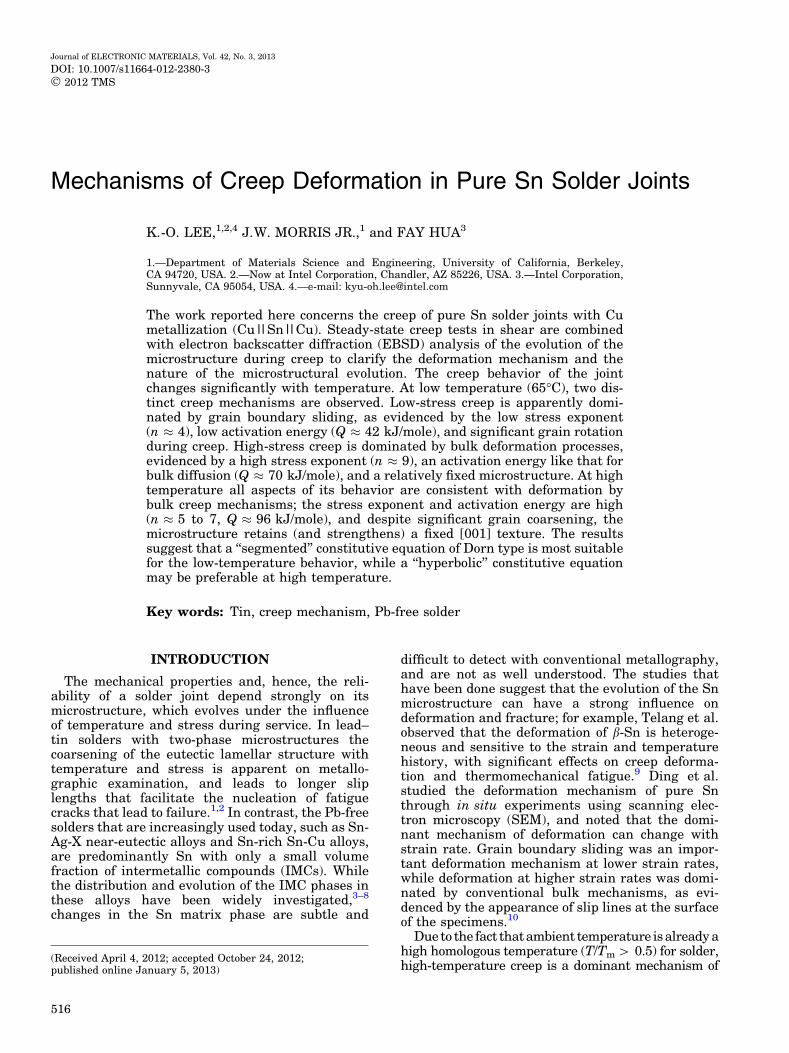
The tests done in this project used single-lapshear specimens like those diagrammed in Fig. 1,with Cu substrates and a pure Sn solder joint. TheCu substrates were prepared from a blank coppersheet on which nine solder pads were patternedusing a solder mask. Pure tin was held in the moltencondition for 5 h and cast on a copper block. Thecast Sn was homogenized for 48 h at 170�C in anoven, and then cold rolled into foils of about 180 lmthickness. An oxygen-free (OHFC) copper plate wasused as the pad metallization of copper. The foilswere cut, placed on the Cu pads between substrates,and reflowed in two steps: 145�C for 5 min and245�C for 8 min, in a programmable furnace with anitrogen gas environment. The hold time used hereis significantly longer than that used in a conven-tional die-attach process (<60 s) because the samplethat we have here is much thicker (�3.18 mm) thanthe conventional die used in the actual chipattachment process (<760 lm).
Creep tests were done in a dead-load creep machinewith temperature controlled by an oil bath. The creepspecimen is held by frictional grips. The displacementof the grips was monitored with a linear variabledifferential transformer (LVDT) that has a detectionlimit of less than 1 lm displacement. The creep ratein shear was measured as a function of stress at threetemperatures: 65�C, 110�C, and 130�C. The reportedshear stress is the load divided by the solder–sub-strate contact area (total area of the wetted pads).The shear strain (simple shear) is the relative dis-placement of the sample plates divided by the solderjoint thickness. The tabulated creep rates are the
steady-state creep rates. After preliminary stressversus strain rate creep data were obtained, creeptests were done at three different combinations ofstress and temperature that were selected to explorethe three different regimes that produced apparentlydifferent behavior in the preliminary tests: low stressand low temperature, high stress and low tempera-ture, and low stress and high temperature.
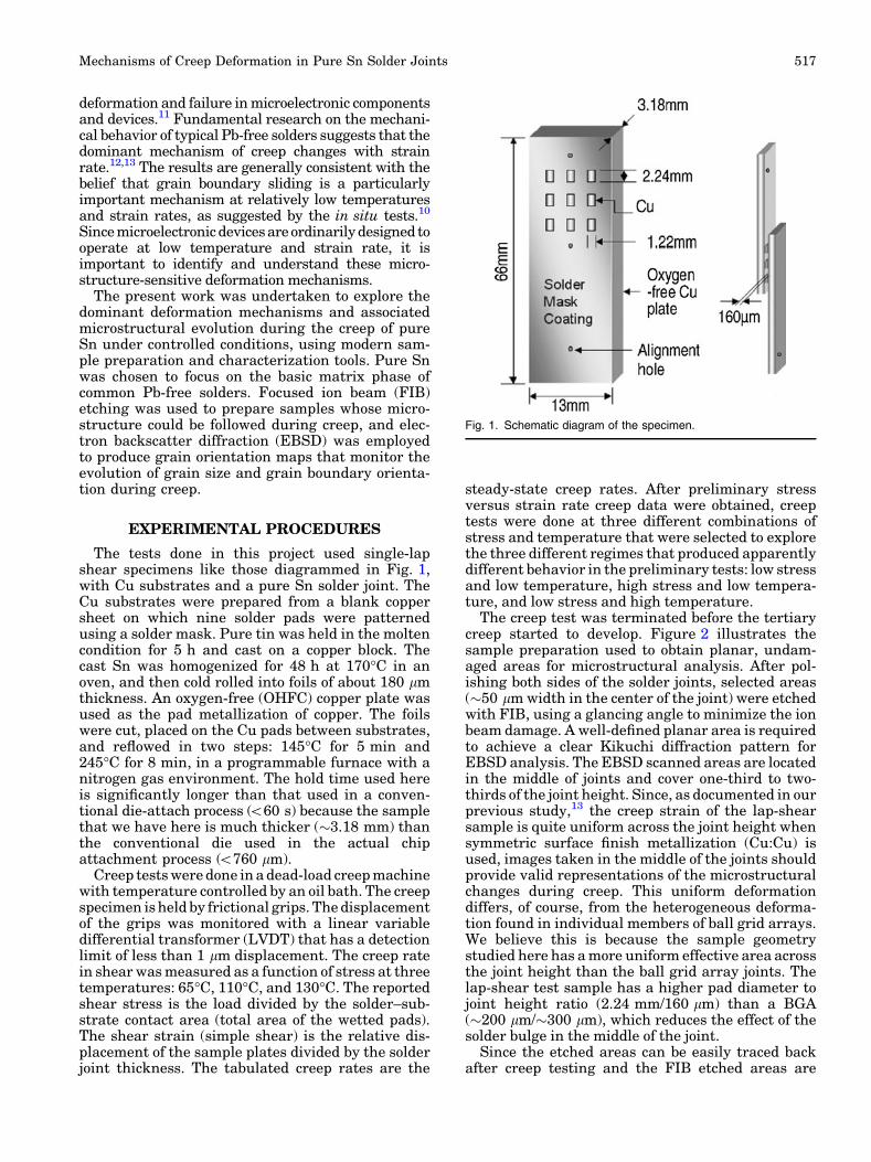
The creep test was terminated before the tertiarycreep started to develop. Figure 2 illustrates thesample preparation used to obtain planar, undam-aged areas for microstructural analysis. After pol-ishing both sides of the solder joints, selected areas(�50 lm width in the center of the joint) were etchedwith FIB, using a glancing angle to minimize the ionbeam damage. A well-defined planar area is requiredto achieve a clear Kikuchi diffraction pattern forEBSD analysis. The EBSD scanned areas are locatedin the middle of joints and cover one-third to two-thirds of the joint height. Since, as documented in ourprevious study,13 the creep strain of the lap-shearsample is quite uniform across the joint height whensymmetric surface finish metallization (Cu:Cu) isused, images taken in the middle of the joints shouldprovide valid representations of the microstructuralchanges during creep. This uniform deformationdiffers, of course, from the heterogeneous deforma-tion found in individual members of ball grid arrays.We believe this is because the sample geometrystudied here has a more uniform effective area acrossthe joint height than the ball grid array joints. Thelap-shear test sample has a higher pad diameter tojoint height ratio (2.24 mm/160 lm) than a BGA(�200 lm/�300 lm), which reduces the effect of thesolder bulge in the middle of the joint.
Since the etched areas can be easily traced backafter creep testing and the FIB etched areas are
Fig. 1. Schematic diagram of the specimen.
Mechanisms of Creep Deformation in Pure Sn Solder Joints 517
almost the same as the EBSD scanned areas, grainorientation maps of the prepared areas could beconstructed before and during the tests (at the endof steady-state creep) to monitor the evolution of theb-Sn microstructure. The microstructural informa-tion obtained included crystallographic orientationand grain shape. The EBSD analysis was done withthe TSL orientation imaging microscopy system.Kikuchi patterns were obtained by the convergentbeam method and analyzed with the software sup-plied with the system for orientation and phasedetermination.14 The obtained datasets werecleaned up by incorporating lower confidence indexpoints with higher confidence index points using anearest-neighbor correlation technique.
RESULTS AND DISCUSSION
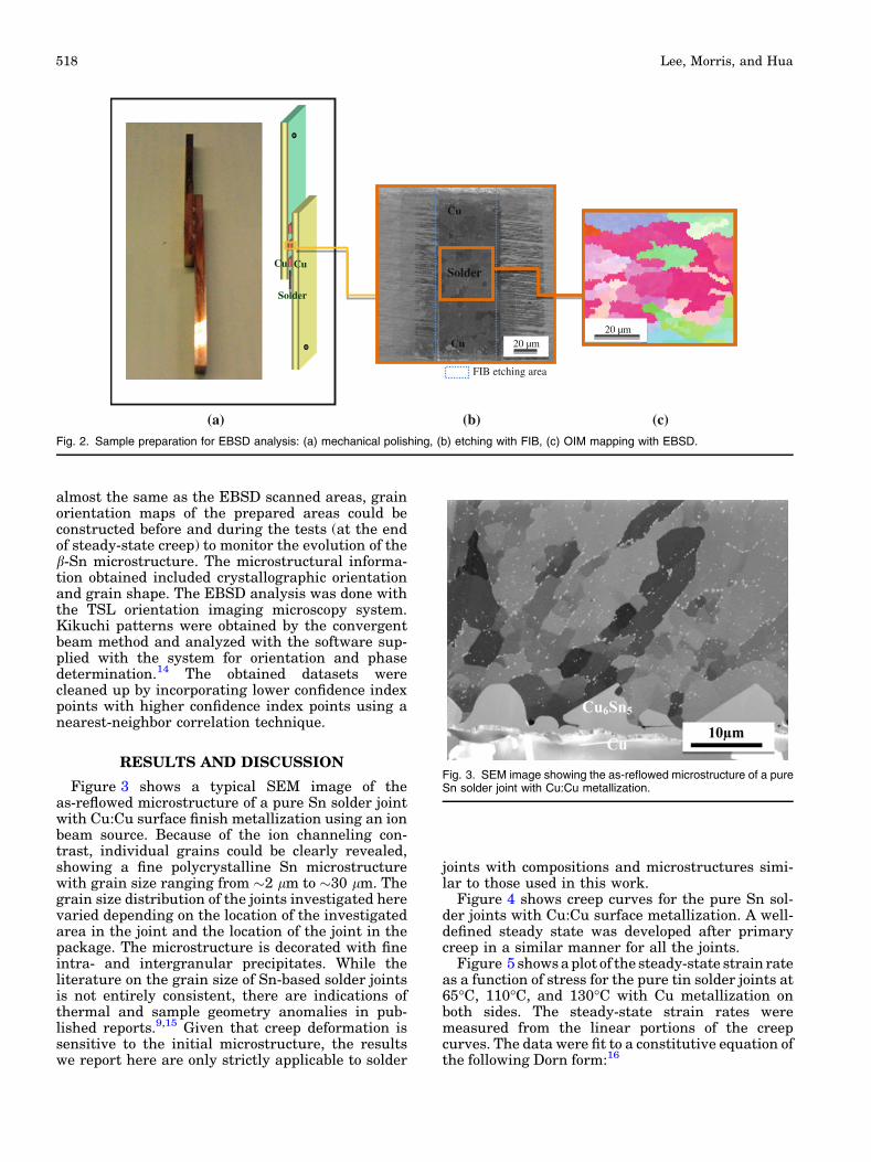
Figure 3 shows a typical SEM image of theas-reflowed microstructure of a pure Sn solder jointwith Cu:Cu surface finish metallization using an ionbeam source. Because of the ion channeling con-trast, individual grains could be clearly revealed,showing a fine polycrystalline Sn microstructurewith grain size ranging from �2 lm to �30 lm. Thegrain size distribution of the joints investigated herevaried depending on the location of the investigatedarea in the joint and the location of the joint in thepackage. The microstructure is decorated with fineintra- and intergranular precipitates. While theliterature on the grain size of Sn-based solder jointsis not entirely consistent, there are indications ofthermal and sample geometry anomalies in pub-lished reports.9,15 Given that creep deformation issensitive to the initial microstructure, the resultswe report here are only strictly applicable to solder
joints with compositions and microstructures simi-lar to those used in this work.
Figure 4 shows creep curves for the pure Sn sol-der joints with Cu:Cu surface metallization. A well-defined steady state was developed after primarycreep in a similar manner for all the joints.
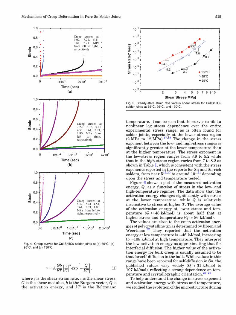
Figure 5 shows a plot of the steady-state strain rateas a function of stress for the pure tin solder joints at65�C, 110�C, and 130�C with Cu metallization onboth sides. The steady-state strain rates weremeasured from the linear portions of the creepcurves. The data were fit to a constitutive equation ofthe following Dorn form:16
Cu
Cu
Solder
(a) (c)
Cu
Solder
Cu
(b)
FIB etching area
20 µm 20 µm
Fig. 2. Sample preparation for EBSD analysis: (a) mechanical polishing, (b) etching with FIB, (c) OIM mapping with EBSD.
Fig. 3. SEM image showing the as-reflowed microstructure of a pureSn solder joint with Cu:Cu metallization.
Lee, Morris, and Hua518
c� ¼ A
Gb
kT
sG
h inexp � Q
kT
� �; (1)
where _c is the shear strain rate, s is the shear stress,G is the shear modulus, b is the Burgers vector, Q isthe activation energy, and kT is the Boltzmann
temperature. It can be seen that the curves exhibit anonlinear log stress dependence over the entireexperimental stress range, as is often found forsolder joints, especially at the lower stress region(2 MPa to 12 MPa).17,18 The change in the stressexponent between the low- and high-stress ranges issignificantly greater at the lower temperature thanat the higher temperature. The stress exponent inthe low-stress region ranges from 3.9 to 5.2 whilethat in the high-stress region varies from 7 to 8.2 asshown in Table I, which is consistent with the stressexponents reported in the reports for Sn and Sn-richsolders, from near 519,20 to around 101,21 dependingupon the stress and temperature tested.
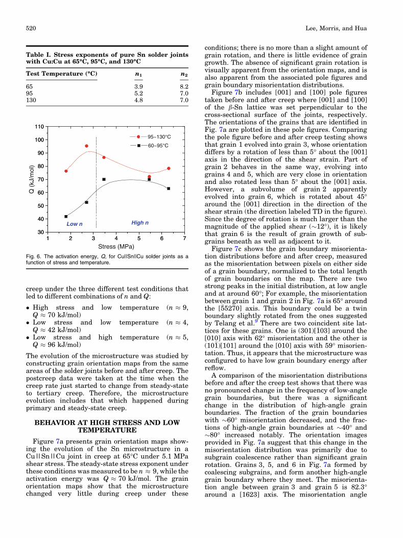
Figure 6 shows a plot of the measured activationenergy, Q, as a function of stress in the low- andhigh-temperature regimes. The data show that theactivation energy changes significantly with stressat the lower temperature, while Q is relativelyinsensitive to stress at higher T. The average valueof the activation energy at lower stress and tem-perature (Q � 48 kJ/mol) is about half that athigher stress and temperature (Q � 86 kJ/mol).
The values are close to the creep activation ener-gies of polycrystalline tin as determined by Breen andWeertman.22 They reported that the activationenergy at low temperature is�46 kJ/mol, increasingto �108 kJ/mol at high temperature. They interpretthe low activation energy as approximating that forinterfacial diffusion. The higher value of the activa-tion energy for bulk creep is usually assumed to bethat for self-diffusion in the bulk. While values in thisrange have been reported for self-diffusion in Sn, thepublished values vary widely (Q � 31 kJ/mol to107 kJ/mol), reflecting a strong dependence on tem-perature and crystallographic orientation.23–26
To help understand the change in stress exponentand activation energy with stress and temperature,we studied the evolution of the microstructure during
10-9
10-8
10-7
10-6
10-5
10-4
10-3
10-2
10-1
1 2 3 4 5 6 7 8 9 10
8.2
3.9
65°C
7.0
n~4.8
130°CStr
ain
Rat
e(1/
sec)
7.0
5.2
95°C
Shear Stress(MPa)
Fig. 5. Steady-state strain rate versus shear stress for Cu||Sn||Cusolder joints at 65�C, 95�C, and 130�C.
0 1x10⁴ 2x10⁴ 3x10⁴
0.0
0.2
0.4
0.6
0.8
1.0S
trai
n
0.0
0.2
0.4
0.6
0.8
1.0
0 1x10⁴ 2x10⁴ 3x10⁴ 4x10⁴
Time (sec)
Time (sec)
0.0 5.0x10³ 1.0x10⁴ 1.5x10⁴ 2.0x10⁴
0.0
0.2
0.4
0.6
0.8
1.0
Time (sec)
Str
ain
Str
ain
(a)
Creep curves at 9.02, 7.22, 5.41 3.61, 2.71 MPa from left to right, respectively
Creep curves at 6.32, 5.41 4.51, 3.61, 2.71, 1.80 MPa from left to right, respectively
Creep curves at 7.22, 6.32, 5.41 4.51, 3.61, 2.71, 1.80 MPa from left to right, respectively
(b)
(c)Fig. 4. Creep curves for Cu||Sn||Cu solder joints at (a) 65�C, (b)95�C, and (c) 130�C.
Mechanisms of Creep Deformation in Pure Sn Solder Joints 519
creep under the three different test conditions thatled to different combinations of n and Q:
� High stress and low temperature (n � 9,Q � 70 kJ/mol)
� Low stress and low temperature (n � 4,Q � 42 kJ/mol)
� Low stress and high temperature (n � 5,Q � 96 kJ/mol)
The evolution of the microstructure was studied byconstructing grain orientation maps from the sameareas of the solder joints before and after creep. Thepostcreep data were taken at the time when thecreep rate just started to change from steady-stateto tertiary creep. Therefore, the microstructureevolution includes that which happened duringprimary and steady-state creep.
BEHAVIOR AT HIGH STRESS AND LOWTEMPERATURE
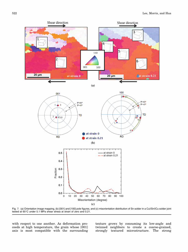
Figure 7a presents grain orientation maps show-ing the evolution of the Sn microstructure in aCu||Sn||Cu joint in creep at 65�C under 5.1 MPashear stress. The steady-state stress exponent underthese conditions was measured to be n � 9, while theactivation energy was Q � 70 kJ/mol. The grainorientation maps show that the microstructurechanged very little during creep under these
conditions; there is no more than a slight amount ofgrain rotation, and there is little evidence of graingrowth. The absence of significant grain rotation isvisually apparent from the orientation maps, and isalso apparent from the associated pole figures andgrain boundary misorientation distributions.
Figure 7b includes [001] and [100] pole figurestaken before and after creep where [001] and [100]of the b-Sn lattice was set perpendicular to thecross-sectional surface of the joints, respectively.The orientations of the grains that are identified inFig. 7a are plotted in these pole figures. Comparingthe pole figure before and after creep testing showsthat grain 1 evolved into grain 3, whose orientationdiffers by a rotation of less than 5� about the [001]axis in the direction of the shear strain. Part ofgrain 2 behaves in the same way, evolving intograins 4 and 5, which are very close in orientationand also rotated less than 5� about the [001] axis.However, a subvolume of grain 2 apparentlyevolved into grain 6, which is rotated about 45�around the [001] direction in the direction of theshear strain (the direction labeled TD in the figure).Since the degree of rotation is much larger than themagnitude of the applied shear (�12�), it is likelythat grain 6 is the result of grain growth of sub-grains beneath as well as adjacent to it.
Figure 7c shows the grain boundary misorienta-tion distributions before and after creep, measuredas the misorientation between pixels on either sideof a grain boundary, normalized to the total lengthof grain boundaries on the map. There are twostrong peaks in the initial distribution, at low angleand at around 60�; For example, the misorientationbetween grain 1 and grain 2 in Fig. 7a is 65� aroundthe [�55270] axis. This boundary could be a twinboundary slightly rotated from the ones suggestedby Telang et al.9 There are two coincident site lat-tices for these grains. One is (301)[�103] around the[010] axis with 62� misorientation and the other is(10�1)[101] around the [010] axis with 59� misorien-tation. Thus, it appears that the microstructure wasconfigured to have low grain boundary energy afterreflow.
A comparison of the misorientation distributionsbefore and after the creep test shows that there wasno pronounced change in the frequency of low-anglegrain boundaries, but there was a significantchange in the distribution of high-angle grainboundaries. The fraction of the grain boundarieswith �60� misorientation decreased, and the frac-tions of high-angle grain boundaries at �40� and�80� increased notably. The orientation imagesprovided in Fig. 7a suggest that this change in themisorientation distribution was primarily due tosubgrain coalescence rather than significant grainrotation. Grains 3, 5, and 6 in Fig. 7a formed bycoalescing subgrains, and form another high-anglegrain boundary where they meet. The misorienta-tion angle between grain 3 and grain 5 is 82.3�around a [1623] axis. The misorientation angle
Table I. Stress exponents of pure Sn solder jointswith Cu:Cu at 65�C, 95�C, and 130�C
Test Temperature (�C) n1 n2
65 3.9 8.295 5.2 7.0130 4.8 7.0
1 2 3 4 5 6 730
40
50
60
70
80
90
100
110
1 2 3 4 5 6 730
40
50
60
70
80
90
100
110
Low n
Q (
kJ/m
ol)
Stress (MPa)
60~95°C
High n
95~130°C
Fig. 6. The activation energy, Q, for Cu||Sn||Cu solder joints as afunction of stress and temperature.
Lee, Morris, and Hua520

between grain 5 and grain 6 is 42.6� around [42�27]axis. The grain boundaries that disappeared duringcoalescence were predominantly those with smallangle misorientations or misorientations near 60�,which would seem to reflect the higher mobility oflow-angle and twin boundaries.
This microstructure development observed heresuggests, and is consistent with, a conventional bulkdeformation mechanism that involves dislocationglide assisted by dislocation climb. It is common tofind a high stress exponent and an activation energynear that for bulk diffusion in this case, and con-ventional dislocation mechanisms do not necessarilyproduce significant grain rotations or grain bound-ary misorientations.
BEHAVIOR AT LOW STRESS AND LOWTEMPERATURE
Figure 8a presents grain orientation maps for asample crept at 65�C under shear stress of 1.4 MPa.This combination leads to low stress/low tempera-ture behavior; the measured stress exponent underthese conditions is n � 4, and the activation energyis Q � 42 kJ/mole.
As shown in Fig. 8a, the microstructure of thematerial changed dramatically during this test. Thegrain size increased by a factor of 2 or more.The several low-angle boundaries that appear in theinitial microstructure disappeared, and the grainswere rotated into or replaced by new grains withrelatively high-angle boundaries and no obvious ori-entational correspondence with the original grains.
Figure 8b shows the change in the [001] and [100]pole figures during the test. The original sample hada texture very similar to that found in the previouscase (Fig. 7b). However, the pole figure changed sig-nificantly during creep without a systematic pattern.Grain 2 rotated to grain 6 about 90� around [110]direction. Grain 3 and a part of grain 4 rotated tograin 7 and grain 8 about 45� around [100] direction.The rest of grain 4 rotated about 100� around [110]direction in the shear direction. The microstructureevolved (grain 2 and 4 to grain 6, 7, 8, and 9) to lowerenergy during creep by aligning highly facile slipsystems, (110)[001], closer to the shear direction.27
The change in grain boundary character during creepis also apparent in the misorientation distribution(Fig. 8c). The pronounced peak in the orientationalfrequency at �60� decreases substantially, and isreplaced by a distribution that is almost flat for an-gles greater than 5�. The original peak near 60� is dueto the frequency of twin boundaries, such as thatbetween the grains numbered 2 and 4 in Fig. 8a.While deformation at high stress caused theappearance of new, reasonably well-defined peaksnear 40� and 80�, the final, low-stress distribution ismore uniform, suggesting a nearly random distribu-tion of misalignment angles.
The combination of low stress exponent, lowactivation energy, and substantial grain rotation is
consistent with creep deformation whose rate isdominated by grain boundary sliding, rotatinggrains into the orientation that is most compatiblewith the applied stress irrespective of their mis-match with neighboring grains.
This result is physically reasonable. Grain boundarysliding is a common deformation mode at low stress andtemperature, since bulk dislocation plasticity is diffi-cult and grain boundary sliding only requires disloca-tion plasticity at nodal points in the grain boundarynetwork. Grain rotation into the direction mostcompatible with the applied stress is favored since theassociated decrease in energy assists the relativelysmall applied stress to accomplish the deformation.Rotation away from the most favorable orientation isdifficult since the small applied stress has difficultyovercoming the associated energy barrier and, at lowtemperature, there is limited thermal energy availableto assist.
BEHAVIOR AT LOW STRESS AND HIGHTEMPERATURE
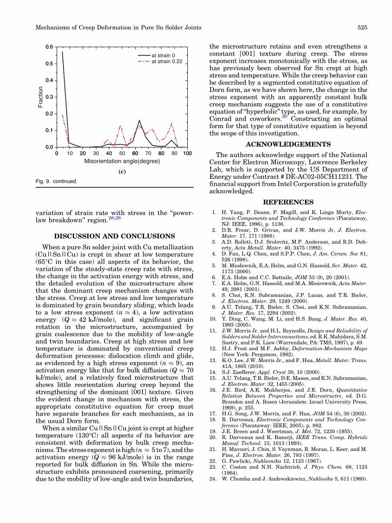
Figure 9a presents grain orientation maps for thesolder joints that were crept at 130�C under 2.7 MPaapplied stress. This composition represents low stress/high temperature behavior: the stress exponent isn � 5, and the activation energy is Q � 96 kJ/mol.
In this case also the microstructure changes dra-matically during the test. As shown in Fig. 9a, c, thestarting microstructure has a preponderance of low-angle boundaries and twin boundaries. Duringcreep the grain size coarsens significantly. The datain Fig. 9a, c show that this happens through pref-erential elimination of low-angle and twin bound-aries to create a microstructure in which the grainboundary misorientations are almost random.
Figure 9b shows the change in the [001] and [100]pole figures during the test. Comparing the grainorientation between grain 1 and 9 and grain 8 and14, there is no noticeable grain rotation duringcreep tests. However, grain 7 rotated to grain 13about 45� around the [100] direction. Grains 4, 5,and 6 coalesced to grain 12. Interestingly, grains 4and 6 rotated to grain 12 about 45� around [100] inthe approximately surface normal direction, RD,while grain 5 rotated to grain 12 about 45� around[100] in the direction of the shear. This result showsthat the grains that grow preferentially tend toshare a common [001] axis, and that they grow byconsuming those grains than are misoriented fromthem by low-angle or twin relations, but have off-texture [001] axes. The process continues until itproduces a highly textured microstructure of rela-tively immobile grain boundaries with almost ran-dom misorientations.
Therefore, the initial microstructure (Fig. 9a) ismade of clusters of grains with low-angle or twinorientations (the product of thermal aging) thathave essentially random overall misorientations
Mechanisms of Creep Deformation in Pure Sn Solder Joints 521
with respect to one another. As deformation pro-ceeds at high temperature, the grain whose [001]axis is most compatible with the surrounding
texture grows by consuming its low-angle andtwinned neighbors to create a coarse-grained,strongly textured microstructure. The strong
(b)
(a)
0 10 20 30 40 50 60 70 80 90 1000.0
0.1
0.2
0.3
0.4
0.5 at strain 0
Fra
ctio
n
Misorientation (degree)
0.0
0.1
0.2
0.3
0.4
0.5 at strain 0.21
(c)Fig. 7. (a) Orientation image mapping, (b) [001] and [100] pole figures, and (c) misorientation distribution of Sn solder in a Cu||Sn||Cu solder jointtested at 65�C under 5.1 MPa shear stress at strain of zero and 0.21.
Lee, Morris, and Hua522

texture minimizes strain by aligning the tetragonalaxes of the Sn grains.
Once the highly mobile low-angle and twinboundaries have disappeared, the coarse-grained
structure appears to creep by bulk dislocationmechanisms, as indicated by its high activationenergy and retained texture. This conclusion issupported further by the relatively small change in
(b)
0 10 20 30 40 50 60 70 80 90 100
at strain 0.20
Misorientation (degree)
0.0
0.1
0.2
0.3
0.4
0.5 at strain 0
Fra
ctio
n
(c)
(a)
Fig. 8. (a) Orientation image mapping, (b) [001] and [100] pole figures, and (c) misorientation distribution of Sn solder in a Cu||Sn||Cu solder jointtested at 65�C under 1.4 MPa shear stress at strain of zero and 0.20.
Mechanisms of Creep Deformation in Pure Sn Solder Joints 523
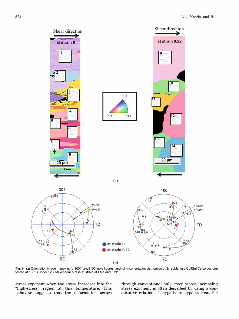
stress exponent when the stress increases into the‘‘high-stress’’ region at this temperature. Thisbehavior suggests that the deformation occurs
through conventional bulk creep whose increasingstress exponent is often described by using a con-stitutive relation of ‘‘hyperbolic’’ type to treat the
(b)
(a)
Fig. 9. (a) Orientation image mapping, (b) [001] and [100] pole figures, and (c) misorientation distribution of Sn solder in a Cu||Sn||Cu solder jointtested at 130�C under 12.7 MPa shear stress at strain of zero and 0.22.
Lee, Morris, and Hua524
variation of strain rate with stress in the ‘‘power-law breakdown’’ region.28,29
DISCUSSION AND CONCLUSIONS
When a pure Sn solder joint with Cu metallization(Cu||Sn||Cu) is crept in shear at low temperature(65�C in this case) all aspects of its behavior, thevariation of the steady-state creep rate with stress,the change in the activation energy with stress, andthe detailed evolution of the microstructure showthat the dominant creep mechanism changes withthe stress. Creep at low stress and low temperatureis dominated by grain boundary sliding, which leadsto a low stress exponent (n � 4), a low activationenergy (Q � 42 kJ/mole), and significant grainrotation in the microstructure, accompanied bygrain coalescence due to the mobility of low-angleand twin boundaries. Creep at high stress and lowtemperature is dominated by conventional creepdeformation processes: dislocation climb and glide,as evidenced by a high stress exponent (n � 9), anactivation energy like that for bulk diffusion (Q � 70kJ/mole), and a relatively fixed microstructure thatshows little reorientation during creep beyond thestrengthening of the dominant [001] texture. Giventhe evident change in mechanism with stress, theappropriate constitutive equation for creep musthave separate branches for each mechanism, as inthe usual Dorn form.
When a similar Cu||Sn||Cu joint is crept at highertemperature (130�C) all aspects of its behavior areconsistent with deformation by bulk creep mecha-nisms. The stress exponent ishigh (n � 5 to7), and theactivation energy (Q � 96 kJ/mole) is in the rangereported for bulk diffusion in Sn. While the micro-structure exhibits pronounced coarsening, primarilydue to the mobility of low-angle and twin boundaries,
the microstructure retains and even strengthens aconstant [001] texture during creep. The stressexponent increases monotonically with the stress, ashas previously been observed for Sn crept at highstress and temperature. While the creep behavior canbe described by a segmented constitutive equation ofDorn form, as we have shown here, the change in thestress exponent with an apparently constant bulkcreep mechanism suggests the use of a constitutiveequation of ‘‘hyperbolic’’ type, as used, for example, byConrad and coworkers.30 Constructing an optimalform for that type of constitutive equation is beyondthe scope of this investigation.
ACKNOWLEDGEMENTS
The authors acknowledge support of the NationalCenter for Electron Microscopy, Lawrence BerkeleyLab, which is supported by the US Department ofEnergy under Contract # DE-AC02-05CH11231. Thefinancial support from Intel Corporation is gratefullyacknowledged.
REFERENCES
1. H. Yang, P. Deane, P. Magill, and K. Linga Murty, Elec-tronic Components and Technology Conference (Piscataway,NJ: IEEE, 1996), p. 1136.
2. D.R. Frear, D. Grivas, and J.W. Morris Jr, J. Electron.Mater. 17, 171 (1988).
3. A.D. Rollett, D.J. Srolovitz, M.P. Anderson, and R.D. Doh-erty, Acta Metall. Mater. 40, 3475 (1992).
4. D. Fan, L.Q. Chen, and S.P.P. Chen, J. Am. Ceram. Soc 81,526 (1998).
5. M. Miodownik, E.A. Holm, and G.N. Hassold, Scr. Mater. 42,1173 (2000).
6. E.A. Holm and C.C. Battaile, JOM 53 (9), 20 (2001).7. E.A. Holm, G.N. Hassold, and M.A. Mioirownik, Acta Mater.
49, 2981 (2001).8. S. Choi, K.N. Subramanian, J.P. Lucas, and T.R. Bieler,
J. Electron. Mater. 29, 1249 (2000).9. A.U. Telang, T.R. Bieler, S. Choi, and K.N. Subramanian,
J. Mater. Res. 17, 2294 (2002).10. Y. Ding, C. Wang, M. Li, and H.S. Bang, J. Mater. Res. 40,
1993 (2005).11. J.W. Morris Jr. and H.L. Reynodls, Design and Reliability of
Solders and Solder Interconnections, ed. R.K. Mahidara, S.M.Sastry, and P.K. Liaw (Warrendale, PA: TMS, 1997), p. 49.
12. H.J. Frost and M.F. Ashby, Deformation-Mechanism Maps(New York: Pergamon, 1982).
13. K.O. Lee, J.W. Morris Jr., and F. Hua, Metall. Mater. Trans.41A, 1805 (2010).
14. S.J. Zaefferer, Appl. Cryst 30, 10 (2000).15. A.U. Telang, T.R. Bieler, D.E. Mason, and K.N. Subramanian,
J. Electron. Mater. 32, 1455 (2005).16. J.E. Bird, A.K. Mukherjee, and J.E. Dorn, Quantitative
Relation Between Properties and Microstructre, ed. D.G.Brandon and A. Rosen (Jerusalem: Israel University Press,1969), p. 255.
17. H.G. Song, J.W. Morris, and F. Hua, JOM 54 (6), 30 (2002).18. R. Darveaux, Electronic Components and Technology Con-
ference (Piscataway: IEEE, 2005), p. 882.19. J.E. Breen and J. Weertman, J. Met. 72, 1230 (1955).20. R. Darveaux and K. Banerji, IEEE Trans. Comp. Hybrids
Manuf. Technol. 15, 1013 (1993).21. H. Mavoori, J. Chin, S. Vaynman, B. Moran, L. Keer, and M.
Fine, J. Electron. Mater. 26, 783 (1997).22. G. Pawlicki, Nukleonika 12, 1123 (1967).23. C. Coston and N.H. Nachtrieb, J. Phys. Chem. 68, 1123
(1964).24. W. Chomba and J. Andewskiewicz, Nukleoika 5, 611 (1960).
0 20 40 60 80 1000.0
0.1
0.2
0.3
0.4
0.5
0.6
at strain 0
Fra
ctio
n
Misorientation angle(degree)0 10 20 30 40 50 60 70 80 90 100
0.0
0.1
0.2
0.3
0.4
0.5
0.6
at strain 0.22
(c)Fig. 9. continued.
Mechanisms of Creep Deformation in Pure Sn Solder Joints 525

25. V. Raman and R. Berriche, J. Mater. Res. 7, 627 (1992).26. S.N.G. Chu and J.C.M. Li, Mater. Sci. Eng. 39, 1 (1979).27. M. Fujiwara and T. Hirokawa, J. Jpn. Inst. Met. 51, 830
(1987).28. F. Garofalo, Fundamentals of Creep and Creep-Rupture in
Metals (New York: Macmillan, 1965).
29. A. Schubert, H. Walter, R. Dudek, B. Michel, G. Lefranc, J.Otto, and G. Mitic, Proceedings, 2001 International Sym-posium on Advanced Packaging Materials (2001), p. 129.
30. P.L. Hacke, A.F. Sprecher, and H. Conrad, Thermal Stressand Strain in Microelectronic Packaging, ed. J. Lau (NewYork: Van Nostrand Reinold, 1994), p. 466.
Lee, Morris, and Hua526