mechanical and optical properties of hard sicn coatings prepared by pecvd
TRANSCRIPT
Thin Solid Films 447–448(2004) 201–207
0040-6090/04/$ - see front matter� 2003 Elsevier B.V. All rights reserved.doi:10.1016/S0040-6090Ž03.01057-5
Mechanical and optical properties of hard SiCN coatings prepared byPECVD
P. Jedrzejowski , J. Cizek , A. Amassian , J.E. Klemberg-Sapieha *, J. Vlcek , L. Martinua b a a, b a
Groupe de recherche en physique et technologie des couches minces (GCM) and Department of Engineering Physics, Ecole Polytechnique,a
2900, boul. Edouard-Montpetit, Montreal, Quebec, Canada, H3C 3A7Department of Physics, University of West Bohemia, Univerzitni 22, Plzen 306 14, Czech Republicb
Abstract
Novel amorphous SiCN coatings are becoming increasingly attractive because of their mechanical, optical and electronicproperties. In the present work, SiCN films were fabricated by PECVD from SiHyCH yN yAr gas mixtures at a temperature of4 4 2
400 8C. Mechanical properties such as hardness, Young’s modulus, friction coefficient and stress were evaluated, respectively, bydepth-sensing indentation, pin-on-disk, micro-scratch and curvature methods. Films deposited under optimized conditions exhibiteda hardness)30 GPa, Young’s modulus)190 GPa, elastic rebound of 85% and a compressive stress of approximately 1 GPa. Afriction coefficient against Al O , ranging from 0.75 to 0.25 and a low surface roughness of approximately 1 nm were found to2 3
be accompanied by a refractive index ranging from 1.85 to 2.10(at 550 nm) and an extinction coefficient between 1.0=10y4
and 4.5=10 . The film behavior is correlated with the microstructure and composition determined by SEM, XPS, AFM andy2
broad-range UV–VIS–NIR–IR spectroscopic ellipsometry.� 2003 Elsevier B.V. All rights reserved.
Keywords: PECVD; SiCN; Mechanical properties; Spectroscopic ellipsometry; Microstructure
1. Introduction
In recent years, ternary silicon carbon nitrides(SiCN)have attracted considerable interest due to their excep-tional mechanical, tribological and optical properties.Chemical inertness and high hardnessw1–4x make SiCNceramics a promising option for new micro-electrome-chanical systems(MEMS) w5x. Good wetting behaviorw6x, attractive tribological propertiesw7x and high tem-perature oxidation resistancew8x offer many other appli-cations in coating technologies. ‘Tunable’ band gapcharacteristics(band gap engineering) w1,9,10x, adjust-able transparency in the visible and IR regionsw11–13xand high thermal stabilityw14x make them attractive formicroelectronics and optoelectronics.SiCN can be formed by combining binary materials,
such as SiN , SiC and CN. Each of these three1.3
materials provides the following intrinsic property:SiN is a highly transparent, wide band gap(approx.1.3
*Corresponding author. Tel.:q1-514-340-5747; fax:q1-514-340-3218.
E-mail address: [email protected](J.E. Klemberg-Sapieha).
5 eV) dielectric w15,16x. SiC possesses a lower bandgap (approx. 2.8 eV) and is characterized by excellentmechanical performancew16,17x and CN contributeshigh hardness, partial electrical conductivity and highelastic reboundw18x due to a fullerene-like microstruc-ture w19x. These three materials form solid solutionw20x.Therefore, by changing the phase content and by con-trolling the short range order it is possible to tune theproperties of SiCN films to specific applications. Inaddition, this ternary material also possesses a complexchemical structure containing Si, C and N.SiCN films have been prepared by various techniques,
which include: pyrolysis of polymer precursorsw8x,chemical vapor deposition(CVD) at elevated tempera-tures w2x, bias-assisted hot filament CVDw21x, radiofrequency plasma-enhanced CVD(PECVD) w22,23x,microwave PECVD w24,25x, electron cyclotron reso-nance PECVDw9–11x, pulsed laser depositionw4,12x,ion beam sputteringw3,26x and reactive magnetronsputteringw6,27,28x.Although, many significant and encouraging results
have been reported on ternary SiCN films, optimizationof the optical and mechanical performance and micro-
202 P. Jedrzejowski et al. / Thin Solid Films 447 –448 (2004) 201–207
Table 1Deposition conditions for PECVD SiCN films
Process Time Substrate temperature Pressure Bias voltage Gas flow(sccm)(min) (8C) (Pa) (V)
Ar N2 SiH4 CH4
Pretreatment(1) 10 400 7 –600 60 – – –Pretreatment(2) 30 400 7 –600 10 25 – –Deposition of SiCN 90 400 13 –600 8 35 5 0–60
structure has not yet been fully explored. PECVDtechnique offers an attractive opportunity to fabricateamorphous hydrogenated SiCN films at intermediatesubstrate temperatures and it provides high quality filmswith good adhesion, good coverage of complicatedsubstrate shapes and high deposition rate. In the presentwork, we specifically focus on the correlation betweenprocess parameters, structure, mechanical, tribologicaland optical properties of these films. Our methodologicalapproach is based on the enhancement of the mechanicalproperties of SiN by adding CN and SiC components1.3 x
in anticipation of obtaining a hard material with a wideband gap and with suitable optical and electroniccharacteristics.
2. Experimental methodology
2.1. Film deposition
SiCN films were deposited in a radio frequency(RF,13.56 MHz) plasma system in which the substrates wereheld on an RF powered electrode(15 cm in diameter).An RF-induced negative DC self-bias,V , developed onB
the electrode. The substrate holder was heated to 4008C using halogen lamps. SiH , CH , N and Ar working4 4 2
gases were introduced via circular distributors. Theirflow was controlled by MKS mass-flow controllers ineach line and the working pressure was measured by acapacitance gauge(MKS Baratron). Prior to deposition,the system was evacuated to 10 Pa using a turbomo-y3
lecular pump.The film fabrication process consisted of two plasma
pretreatment steps in Ar and in N for 10 and 20 min,2
respectively, followed by a 1.5 h long deposition usingthe conditions summarized in Table 1. The choice ofprocess parameters resulted from a preliminary optimi-zation study, which obtained high quality SiN with1.3
respect to its optical and mechanical propertiesw15x. Inall depositions, the conditions were held constant, whilethe concentration of carbon(C) in SiN was controlled1.3
by adjusting the flow of CH (F ) between 0 sccm4 CH4
(pure SiN ) and 60 sccm. Film thickness, measured by1.3
Sloan Dektak II profilometer and a variable anglespectroscopic ellipsometer(VASE, J.A. Woollam Co.)was between 1.0 and 1.5mm. Based on our earlierstudies of ion fluxes and ion energy distribution func-tions in the same reactorw29x, we estimated that the ion
current density during the film growth was approximate-ly 150 mAycm . Crystalline silicon(c-Si) (100) was2
used as substrate and was cleaned prior to deposition inan ultrasonic bath with acetone and isopropanol toeliminate organic surface contaminants.
2.2. Composition characterization
Chemical composition and chemical structure wereanalyzed, respectively, by X-ray photoelectron spectros-copy (XPS) and infrared variable angle spectroscopicellipsometry(IR VASE). XPS analysis was carried outin a VG ESCALAB 3 Mark II instrument with a non-monochromated MgK source(1256.6 eV) with a 0.8a
eV resolution. The IR VASE spectra were measuredbetween 2.5 and 34mm (i.e. approx. from 4000 to 220cm ) using 5 angles of incidence between 65 and 758.y1
Similar to VIS VASE, these measurements were takenin reflection; therefore, the influence of substrate absorp-tion, which is a critical factor in standard FTIR spec-troscopy, was eliminated. Contrary to FTIRmeasurements, IR VASE(and ellipsometry in general)did not directly measure the absorption coefficienta,but it was determined from a simulation of the opticalbehavior in the IR region. The physical model used forIR VASE data consisted of a c-Si substrate with a nativeSiO layer, 3 nm thick, a ‘general oscillator’ and a2
surface roughness layer. In the ‘general oscillator’ mod-el, interband absorptions were simulated by Lorentz-type oscillators; their parameters were found using theLevenberg–Marquardt algorithm during a fitting proce-dure. In addition, inhomogeneities in the optical con-stants throughout the film thickness were modeled by‘mixing’ the optical response of the pure material withvoids. Detected inhomogeneities were not larger than10%. Film morphology was also assessed by scanningelectron microscopy(SEM, Philips XL 20) and byAtomic Force Microscopy(AFM, Digital Instruments,2=2 mm scanned surface).
2.3. Optical and mechanical properties
The refractive index,n, and extinction coefficient,k,were determined by VASE in the visible(VIS) and nearinfrared(NIR) regions between 300 and 1600 nm usingangles of incidence of 558, 658 and 758. The optical
203P. Jedrzejowski et al. / Thin Solid Films 447 –448 (2004) 201–207
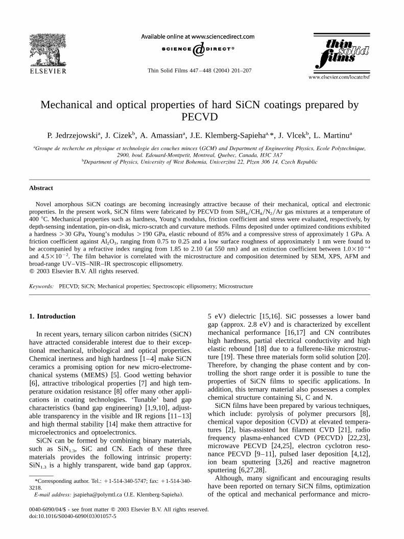
Fig. 1. High resolution XPS spectra of C1s and Si2p core levels forCH gas flows of 0, 3.5, 15 and 60 sccm.4
Table 2Elemental composition measured by XPS
CH flow4 Elemental composition(at.%)(sccm)
Si N C O
0 37.1 45.9 9.0 8.00.75 30.8 37.6 21.0 10.63.5 34.9 28.0 25.6 11.57.0 31.2 32.6 27.0 9.215 25.1 38.1 28.0 7.830 31.0 25.8 31.2 12.060 32.0 22.0 35.0 11.0
data were fitted using the WVASE software(J.A. Wool-lam Co. Inc.) and the same model as for IR VASE.The hardness,H, and reduced Young’s modulus,E ,r
were assessed by depth-sensing indentation using aTriboindenter(Hysitron Inc.) equipped with a Berkovichpyramid and using the Oliver and Pharrw30x methodfor data analysis. Since, the methodology of mechanicaltesting of very hard films with a pronounced elasticresponse is controversial, we performed a detailed anal-ysis of the depth-sensing indentation procedurew31x.This included evaluation of the effects of indentationload, depth of penetration and assessment of the indenterarea function. The results presented in this work wereobtained from 10 indentations using a load ranging from3 to 10 mN.Film stress was obtained from the curvature of silicon
substrates before and after deposition, using a SloanDEKTAK II profilometer and the Stoney formulaw32x.The stress measurements were performed on siliconwafer stripes, which were 30 mm long, 5 mm wide and0.3 mm thick. The friction coefficient,m, at roomtemperature(approx. 258C) and a relative humidity ofapproximately 55% was evaluated using pin-on-disctribometer and micro-scratch tester(CSEM, Neuchatel).The tribometer was equipped with a 6 mm diameterAl O ball. In all experiments, the applied load was2 3
0.25 N and the sliding speed was 10 cm s . The valuesy1
of m reported here refer to the steady-state conditions.In all cases, the travelled distance was greater than 50m. The micro-scratch tester was equipped with a 200mm radius Rockwell C diamond stylus. The appliedload was 1 N andm was measured along a distance of10 mm.
3. Results and discussion
3.1. Structural characterization
The results of XPS compositional analysis are shownin Table 2. The high-resolution XPS spectra of C1s andSi2p core level peaks are presented in Fig. 1 and Table3 for pure SiN and SiCN with differentF . The1.3 CH4
Si2p spectrum for pure SiN showed a presence of1.3
Si–N bonds at 101.6 eV and the contribution of Si–Ox
bonds at 103.0 eV due to surface contamination. WhenCH was added, the Si–C bond at 100.4 eV appeared.4
The C1s spectrum for SiCN was deconvoluted into fivecomponents due to C–Si at 283.4 eV, C–C or C–H at285.0 eV, C–N at 286.0 eV(C–O was also possible),C_N at 287.0 eV (C_O was also possible) andO–C_O at 289.0 eV chemical bondsw33x. The N1sspectrum at 397.6–400.2 eV exhibited a broad peak,difficult to deconvolute due to overlapping of differentN- containing groups(not shown here).Complementary information about the chemical struc-
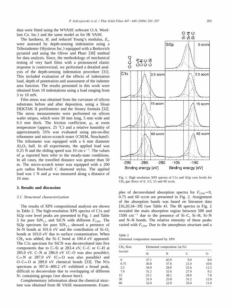
ture was obtained from IR VASE measurements. Exam-
ples of deconvoluted absorption spectra forF s0,CH4
0.75 and 60 sccm are presented in Fig. 2. Assignmentof the absorption bands was based on literature dataw16,20,34–39x (see Table 4). The IR spectra in Fig. 2revealed the main absorption region between 500 and1500 cm due to the presence of Si–C, Si–H, Si–Ny1
and N–H bonds. The relative intensity of these peaksvaried withF . Due to the amorphous structure and aCH4
204 P. Jedrzejowski et al. / Thin Solid Films 447 –448 (2004) 201–207
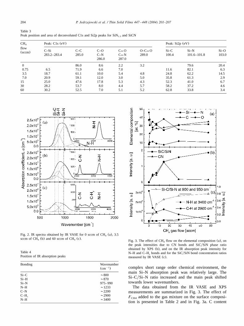
Table 3Peak position and area of deconvoluted C1s and Si2p peaks for SiN and SiCN1.3
CH4 Peak: C1s(eV) Peak: Si2p(eV)flow
C–Si C–C C–O C_O O–C_O Si–C Si–N Si–O(sccm)283.2–283.4 285.0 C–N C_N 289.0 100.4 101.6–101.8 103.0
286.0 287.0
0 86.0 8.6 2.2 3.2 79.6 20.40.75 6.5 71.9 6.6 7.0 11.6 82.1 6.33.5 18.7 61.1 10.0 5.4 4.8 24.8 62.2 14.57.0 20.9 59.1 12.0 3.0 5.0 35.8 61.3 2.915 25.0 47.6 17.8 5.3 4.3 52.3 41.0 6.730 28.2 53.7 8.0 4.4 5.7 58.2 37.2 4.660 30.2 52.5 7.0 5.1 5.2 62.8 33.8 3.4
Fig. 2. IR spectra obtained by IR VASE for 0 sccm of CH(a), 3.54
sccm of CH (b) and 60 sccm of CH(c).4 4 Fig. 3. The effect of CH flow on the elemental composition(a), on4
the peak intensities due to CN bonds and SiCySiN phase ratioobtained by XPS(b), and on the IR absorption peak intensity forN–H and C–H bonds and for the SiCySiN bond concentration ratiosx
measured by IR VASE(c).
Table 4Position of IR absorption peaks
Bonding Wavenumber(cm )y1
Si–C ;800Si–H ;870Si–N 975–990N–H ;1233C–N ;2200C–Hx ;2900N–H ;3400
complex short range order chemical environment, themain Si–N absorption peak was relatively large. TheSi–CySi–N ratio increased and the main peak shiftedtowards lower wavenumbers.The data obtained from the IR VASE and XPS
measurements are summarized in Fig. 3. The effect ofF added to the gas mixture on the surface composi-CH4
tion is presented in Table 2 and in Fig. 3a. C content
205P. Jedrzejowski et al. / Thin Solid Films 447 –448 (2004) 201–207
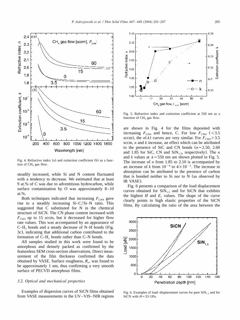
Fig. 4. Refractive index(a) and extinction coefficient(b) as a func-tion of CH gas flow.4
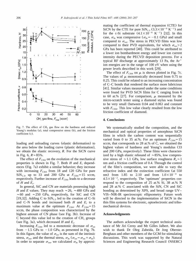
Fig. 5. Refractive index and extinction coefficient at 550 nm as afunction of CH gas flow.4
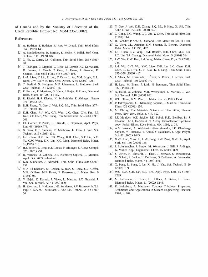
Fig. 6. Examples of load–displacement curves for pure SiN and for1.3
SiCN with Hs33 GPa.
steadily increased, while Si and N content fluctuatedwith a tendency to decrease. We estimated that at least9 at.% of C was due to adventitious hydrocarbon, whilesurface contamination by O was approximately 8–10at.%.Both techniques indicated that increasingF gaveCH4
rise to a steadily increasing Si–CySi–N ratio. Thissuggested that C substituted for N in the chemicalstructure of SiCN. The CN phase content increased withF up to 15 sccm, but it decreased for higher flowCH4
rate values. This was accompanied by an appearance ofC–H bonds and a steady decrease of N–H bonds(Fig.x
3c), indicating that additional carbon contributed to theformation of C–H bonds rather than C–N bonds.x
All samples studied in this work were found to beamorphous and densely packed as confirmed by thefeatureless SEM cross-section observations. Direct meas-urement of the film thickness confirmed the dataobtained by VASE. Surface roughness,R , was found toa
be approximately 1 nm, thus confirming a very smoothsurface of PECVD amorphous films.
3.2. Optical and mechanical properties
Examples of dispersion curves of SiCN films obtainedfrom VASE measurements in the UV–VIS–NIR regions
are shown in Fig. 4 for the films deposited withincreasingF and hence, C. For lowF (-3.5CH4 CH4
sccm), the n(l) curves are very similar. ForF )3.5CH4
sccm,n andk increase, an effect which can be attributedto the presence of SiC and CN bonds(n;2.50, 2.60and 1.85 for SiC, CN and SiN , respectively). The n1.3
andk values atls550 nm are shown plotted in Fig. 5.The increase ofn from 1.85 to 2.10 is accompanied byan increase ofk from 10 to 4=10 . The increase iny4 y2
absorption can be attributed to the presence of carbonthat is bonded neither to Si nor to N(as observed byIR VASE).Fig. 6 presents a comparison of the load displacement
curves obtained for SiN and for SiCN that exhibits1.3
the highestH and E values. The shape of the curver
clearly points to high elastic properties of the SiCNfilms. By calculating the ratio of the area between the
206 P. Jedrzejowski et al. / Thin Solid Films 447 –448 (2004) 201–207
Fig. 7. The effect of CH gas flow on the hardness and reduced4
Young’s modulus(a), total compressive stress(b), and the frictioncoefficient(c).
loading and unloading curves(elastic deformation) tothe area below the loading curve(plastic deformation),we obtain the elastic recovery,R. For the SiCN curvein Fig. 6,R;85%.The effect ofF on the evolution of the mechanicalCH4
properties is shown in Fig. 7. BothH and E depend-r
ences(Fig. 7a) exhibit a similar behavior; they increasewith increasingF from 18 and 120 GPa for pureCH4
SiN , up to 33 and 200 GPa atF s15 sccm,1.3 CH4
respectively. Further increase ofF leads to a decreaseCH4
of H andE .rIn general, SiC and CN are materials possessing high
H andE values. They may reach;26,;480 GPa and;60 and;250 GPa, respectively, for SiC and CNw19,32x. Adding C to SiN led to the creation of C–Si1.3
and C–N bonds and increased bothH and E to ar
maximum value at the optimumF . At F s15CH4 CH4
sccm, the phase composition was characterized by thehighest amount of CN phase(see Fig. 3b). Increase ofC beyond this value led to the creation of CH groupsx
(see Fig. 3a), which decreasedH andE .rIncreasingF led to a monotonic decrease ofsCH4 tot
from y1.5 GPa toy1.0 GPa, as presented in Fig. 7b.In this figure, the value ofs is the sum of the intrinsictot
stress,s , and the thermal stress,s (s ss qs ).int th tot int th
In order to separates , we calculateds by approxi-int th
mating the coefficient of thermal expansion(CTE) forSiCN by the CTE for pure SiN (3.3=10 K ) andy6 y1
1.3
for the c-Si substrate(4.1=10 K ) w32x. In thisy6 y1
case,s was compressive(s sy0.1 GPa) and smallth th
compared tos . The stress in PECVD films was lowtot
compared to their PVD equivalents, for whichs )2tot
GPa has been reportedw40x. This could be attributed toa lower ion bombardment energy and lower ion currentintensity during the PECVD deposition process. For atypical RF discharge at approximately 13 Pa, the Arq
ion energies are in the range of 100 eV when using thepower levels described in this workw29x.The effect ofF on m is shown plotted in Fig. 7c.CH4
The values ofm monotonically decreased from 0.75 to0.25. This could be related to an increasing concentrationof C–C bonds that rendered the surface more lubriciousw41x. Similar values measured under the same conditionswere found for PVD SiCN films for C ranging from 6to 60 at.% w27x. For comparison,m measured by themicro-scratch tester using a diamond stylus was foundto be very small(between 0.04 and 0.06) and constantwith F . This low value clearly resulted from the lowCH4
friction coefficient of diamond.
4. Conclusions
We systematically studied the composition, and themechanical and optical properties of amorphous SiCNfilms in which the carbon content was sequentiallyvaried from 0 to 35 at.%. For an optimumF s15CH4
sccm, that corresponds to 28 at.% of C, we obtained thehighest values of hardness and Young’s modulus(33and 200 GPa, respectively). These films were character-ized by a high elastic rebound of;85%, low compres-sive stress of;1.1 GPa, low surface roughnessR ;1a
nm and a friction coefficient of 0.4. Through the controlof the film’s composition, we were able to vary therefractive index and the extinction coefficient(at 550nm) from 1.85 to 2.10 and from 1.0=10 toy4
4.5=10 , respectively. The ‘optimum’ properties cor-y2
respond to the composition of 25 at.% Si, 38 at.% Nand 28 at.% C associated with the SiN, CN and SiCbonding as determined by XPS, and broad range UV–VIS–NIR-IR spectroscopic ellipsometry. Future workwill be directed to the implementation of SiCN in thethin film systems for electronic, optoelectronic and tribo-mechanical devices.
Acknowledgments
The authors acknowledge the expert technical assis-tance of Mr Jiri Cerny and Mr Gilles Jalbert. We alsowish to thank Dr Oleg Zabeida, Dr Jorg Oberste-Berghaus and other members of the GCM for stimulatingdiscussions. This work was supported by the NaturalSciences and Engineering Research Council(NSERC)
207P. Jedrzejowski et al. / Thin Solid Films 447 –448 (2004) 201–207
of Canada and by the Ministry of Education of theCzech Republic(Project No. MSM 235200002).
References
w1x A. Badzian, T. Badzian, R. Roy, W. Drawl, Thin Solid Films354 (1999) 148.
w2x A. Bendeddouche, R. Berjoan, E. Beche, R. Hillel, Surf. Coat.Technol. 111(1999) 184.
w3x Z. He, G. Carter, J.S. Colligon, Thin Solid Films 283(1996)90.
w4x T. Tharigen, G. Lippold, V. Riede, M. Lorenz, K.J. Koivusaari,¨D. Lorenz, S. Mosch, P. Grau, R. Hesse, P. Streubel, R.Szargan, Thin Solid Films 348(1999) 103.
w5x L.-A. Liew, Y. Liu, R. Luo, T. Cross, L. An, V.M. Bright, M.L.Dunn, J.W. Daily, R. Raj, Sens. Actuat. A 95(2002) 120.
w6x T. Berlind, N. Hellgren, M.P. Johansson, L. Hultman, Surf.Coat. Technol. 141(2001) 145.
w7x E. Bertran, E. Martınez, G. Viera, J. Farjas, P. Roura, Diamond´Relat. Mater. 10(2001) 1115.
w8x R. Riedel, H.-J. Kleebe, H. Schonfelder, F. Aldinger, Nature¨374 (1995) 526.
w9x D.H. Zhang, Y. Gao, J. Wei, Z.Q. Mo, Thin Solid Films 377–378 (2000) 607.
w10x K.H. Chen, J.-J. Wu, C.Y. Wen, L.C. Chen, C.W. Fan, P.F.Kuo, Y.F. Chen, Y.S. Huang, Thin Solid Films 355–356(1999)205.
w11x F.J. Gomez, P. Prieto, E. Elizalde, J. Piquerasa, Appl. Phys.´Lett. 69 (1996) 773.
w12x G. Soto, E.C. Samano, R. Machorro, L. Cota, J. Vac. Sci.Technol. A16(1998) 1311.
w13x L.C. Chen, H.Y. Lin, C.S. Wong, K.H. Chen, S.T. Lin, Y.C.Yu, C.W. Wang, E.K. Lin, K.C. Ling, Diamond Relat. Mater.8 (1999) 618.
w14x H.J. Seifert, J. Peng, H.L. Lukas, F. Aldinger, J. Alloys Compd.320 (2001) 251.
w15x R. Vernhes, O. Zabeida, J.E. Klemberg-Sapieha, L. Martinu,Appl. Opt. 2003, submitted.
w16x K.B. Sundaram, J. Alizadeh, Thin Solid Films 370(2000)151.
w17x M.A. El Khakani, M. Chaker, A. Jean, S. Boily, J.C. Kieffer,M.E. O’Hern, M.F. Ravet, F. Rousseaux, J. Mater. Res. 9(1994) 96.
w18x V. Hajek, K. Rusnak, J. Vlcek, L. Martinu, S.C. Gujrathi, J.Vac. Sci. Technol. A17(1999) 899.
w19x H. Sjostrom, L. Hultman, J.-E. Sundgren, S.V. Hainsworth, T.F.Page, G.S.A.M. Theunissen, J. Vac. Sci. Technol. A14(1996)56.
w20x Y. Gao, J. Wei, D.H. Zhang, Z.Q. Mo, P. Hing, X. Shi, ThinSolid Films 377–378(2000) 562.
w21x Z. Gong, E.G. Wang, G.C. Xu, Y. Chen, Thin Solid Films 348(1999) 114.
w22x H. Sachdev, P. Scheid, Diamond Relat. Mater. 10(2001) 1160.w23x G. Viera, J.L. Andujar, S.N. Sharma, E. Bertran, Diamond´
Relat. Mater. 7(1998) 407.w24x L.C. Chen, C.Y. Yang, D.M. Bhusari, K.H. Chen, M.C. Lin,
J.C. Lin, T.J. Chuang, Diamond Relat. Mater. 5(1996) 514.w25x J.-Y. Wu, C.-T. Kuo, P.-J. Yang, Mater. Chem. Phys. 72(2001)
245.w26x J.-J. Wu, C.-T. Wu, Y.-C. Liao, T.-R. Lu, L.C. Chen, K.H.
Chen, L.-G. Hwa, C.-T. Kuo, K.-J. Ling, Thin Solid Films355–356(1999) 417.
w27x J. Vlcek, M. Kormunda, J. Cızek, V. Perina, J. Zemek, Surf.ˇˇ ´ ˇCoat. Technol. 160(2002) 74.
w28x H. Lutz, M. Bruns, F. Link, H. Baumann, Thin Solid Films332 (1998) 230.
w29x A. Hallil, O. Zabeida, M.R. Wertheimer, L. Martinu, J. Vac.Sci. Technol. A18(2000) 882.
w30x W.C. Oliver, G.M. Pharr, J. Mater. Res. 7(1992) 1564.w31x P. Jedrzejowski, J.E. Klemberg-Sapieha, L. Martinu, Thin Solid
Films 426(2003) 150.w32x M. Ohring, The Materials Science of Thin Films, Plenum
Press, New York, 1992, p. 418, 552.w33x J.F. Moulder, W.F. Stickle, P.E. Sobol, K.D. Boniber, in: J.
Chastain(Ed.), Handbook of X-Ray Photoelectron Spectros-copy, Perkin-Elmer, Eden Prairie, MN, 1992, p. 29.
w34x A.M. Wrobel, A. Walkiewicz-Pietrzykowska, J.E. Klemberg-Sapieha, Y. Hatanaka, T. Aouki, Y. Nakanishi, J. Appl. Polym.Sci. 86(2002) 1445.
w35x X.-C. Xiao, Y.-W. Li, L.-X. Song, X.-F. Peng, X.-F. Hu, Appl.Surf. Sci. 156(2000) 155.
w36x J. Schuhmacher, F. Berger, M. Weinmann, J. Bill, F. Aldinger,K. Muller, Appl. Organomet. Chem. 15(2001) 809.
w37x S. Ulrich, H. Ehrhardt, T. Theel, J. Schwan, S. Westermeyr,M. Scheib, P. Becker, H. Oechsner, G. Dollinger, A. Bergmaier,Diamond Relat. Mater. 7(1998) 839.
w38x X. Peng, L. Song, J. Le, X. Hu, J. Vac. Sci. Technol. B 20(2002) 159.
w39x W.S. Liao, C.H. Lin, S.C. Lee, Appl. Phys. Lett. 65(1994)2229.
w40x M. Lattemann, S. Ulrich, H. Holleck, A. Stuber, H. Leiste,Diamond Relat. Mater. 11(2002) 1248.
w41x K. Holmberg, A. Matthews, Coatings Tribology: Properties,Techniques and Applications in Surface Engineering, Elsevier,1994, p. 209.