mahar biz paper
DESCRIPTION
paperTRANSCRIPT
412 • 2014 IEEE International Solid-State Circuits Conference
ISSCC 2014 / SESSION 24 / INTEGRATED BIOMEDICAL SYSTEMS / 24.1
24.1 A Miniaturized 64-Channel 225µW Wireless Electrocorticographic Neural Sensor
Rikky Muller1,2, Hanh-Phuc Le1, Wen Li1, Peter Ledochowitsch1, Simone Gambini2, Toni Bjorninen3, Aaron Koralek1, Jose M. Carmena1, Michel M. Maharbiz1, Elad Alon1, Jan M. Rabaey1
1University of California, Berkeley, CA, 2University of Melbourne, Parkville, Australia, 3Tampere University of Technology, Tampere, Finland
Substantial improvements in neural-implant longevity are needed to transitionbrain-machine interface (BMI) systems from research labs to clinical practice.While action potential (AP) recording through penetrating electrode arrays offersthe highest spatial resolution, it comes at the price of tissue scarring, resultingin signal degradation over the course of several months [1].Electrocorticography (ECoG) is an electrophysiological technique where electrical potentials are recorded from the surface of the cerebral cortex, reducing cortical scarring. However, today’s clinical ECoG implants are large,have low spatial resolution (0.4 to 1cm) and offer only wired operation.
To enable chronic and stable neural recording, we introduce a minimally invasive, wireless ECoG microsystem. Wireless powering and readout are combined with a microfabricated antenna and electrode grid that has >10× higher electrode density than clinical ECoG arrays, providing spatial resolutionapproaching today’s penetrating electrodes. Area- and power-reduction techniques in the baseband and wireless subsystem result in over 10× IC areareduction with a simultaneous 3× improvement in power efficiency over the stateof the art (see Fig. 24.1.4), enabling a minimally invasive platform for 64-channelrecording. The low power consumption of the IC, together with the antenna integration strategy enables remote powering at 3× below established safety limits [2], while the small size and flexibility of the implant minimizes the foreignbody response. The improved implant safety and longevity gives wireless ECoGexcellent prospects to become the technology of choice for clinically relevantBMIs in the foreseeable future [1].
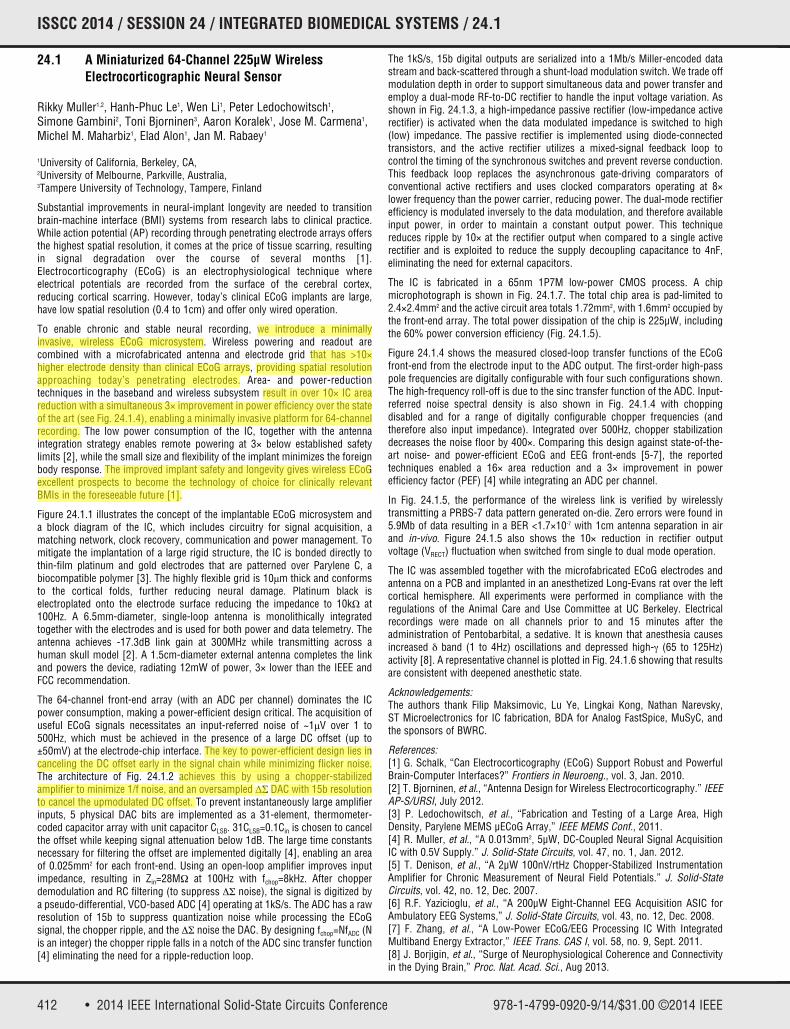
Figure 24.1.1 illustrates the concept of the implantable ECoG microsystem anda block diagram of the IC, which includes circuitry for signal acquisition, amatching network, clock recovery, communication and power management. Tomitigate the implantation of a large rigid structure, the IC is bonded directly tothin-film platinum and gold electrodes that are patterned over Parylene C, a biocompatible polymer [3]. The highly flexible grid is 10μm thick and conformsto the cortical folds, further reducing neural damage. Platinum black is electroplated onto the electrode surface reducing the impedance to 10kΩ at100Hz. A 6.5mm-diameter, single-loop antenna is monolithically integratedtogether with the electrodes and is used for both power and data telemetry. Theantenna achieves -17.3dB link gain at 300MHz while transmitting across ahuman skull model [2]. A 1.5cm-diameter external antenna completes the linkand powers the device, radiating 12mW of power, 3× lower than the IEEE andFCC recommendation.
The 64-channel front-end array (with an ADC per channel) dominates the ICpower consumption, making a power-efficient design critical. The acquisition ofuseful ECoG signals necessitates an input-referred noise of ~1μV over 1 to500Hz, which must be achieved in the presence of a large DC offset (up to±50mV) at the electrode-chip interface. The key to power-efficient design lies incanceling the DC offset early in the signal chain while minimizing flicker noise.The architecture of Fig. 24.1.2 achieves this by using a chopper-stabilized amplifier to minimize 1/f noise, and an oversampled ΔΣ DAC with 15b resolutionto cancel the upmodulated DC offset. To prevent instantaneously large amplifierinputs, 5 physical DAC bits are implemented as a 31-element, thermometer-coded capacitor array with unit capacitor CLSB. 31CLSB=0.1Cin is chosen to cancelthe offset while keeping signal attenuation below 1dB. The large time constantsnecessary for filtering the offset are implemented digitally [4], enabling an areaof 0.025mm2 for each front-end. Using an open-loop amplifier improves inputimpedance, resulting in Zin=28MΩ at 100Hz with fchop=8kHz. After chopperdemodulation and RC filtering (to suppress ΔΣ noise), the signal is digitized bya pseudo-differential, VCO-based ADC [4] operating at 1kS/s. The ADC has a rawresolution of 15b to suppress quantization noise while processing the ECoG signal, the chopper ripple, and the ΔΣ noise the DAC. By designing fchop=NfADC (Nis an integer) the chopper ripple falls in a notch of the ADC sinc transfer function[4] eliminating the need for a ripple-reduction loop.
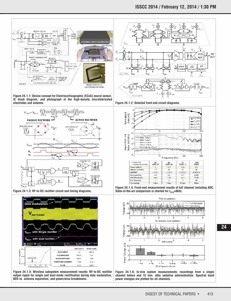
The 1kS/s, 15b digital outputs are serialized into a 1Mb/s Miller-encoded datastream and back-scattered through a shunt-load modulation switch. We trade offmodulation depth in order to support simultaneous data and power transfer andemploy a dual-mode RF-to-DC rectifier to handle the input voltage variation. Asshown in Fig. 24.1.3, a high-impedance passive rectifier (low-impedance activerectifier) is activated when the data modulated impedance is switched to high(low) impedance. The passive rectifier is implemented using diode-connectedtransistors, and the active rectifier utilizes a mixed-signal feedback loop to control the timing of the synchronous switches and prevent reverse conduction.This feedback loop replaces the asynchronous gate-driving comparators of conventional active rectifiers and uses clocked comparators operating at 8×lower frequency than the power carrier, reducing power. The dual-mode rectifierefficiency is modulated inversely to the data modulation, and therefore availableinput power, in order to maintain a constant output power. This techniquereduces ripple by 10× at the rectifier output when compared to a single activerectifier and is exploited to reduce the supply decoupling capacitance to 4nF,eliminating the need for external capacitors.
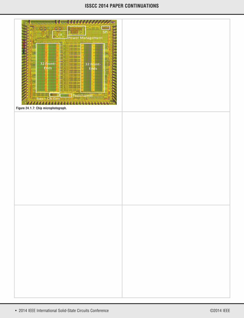
The IC is fabricated in a 65nm 1P7M low-power CMOS process. A chipmicrophotograph is shown in Fig. 24.1.7. The total chip area is pad-limited to2.4×2.4mm2 and the active circuit area totals 1.72mm2, with 1.6mm2 occupied bythe front-end array. The total power dissipation of the chip is 225μW, includingthe 60% power conversion efficiency (Fig. 24.1.5).
Figure 24.1.4 shows the measured closed-loop transfer functions of the ECoGfront-end from the electrode input to the ADC output. The first-order high-passpole frequencies are digitally configurable with four such configurations shown.The high-frequency roll-off is due to the sinc transfer function of the ADC. Input-referred noise spectral density is also shown in Fig. 24.1.4 with chopping disabled and for a range of digitally configurable chopper frequencies (and therefore also input impedance). Integrated over 500Hz, chopper stabilizationdecreases the noise floor by 400×. Comparing this design against state-of-the-art noise- and power-efficient ECoG and EEG front-ends [5-7], the reportedtechniques enabled a 16× area reduction and a 3× improvement in power efficiency factor (PEF) [4] while integrating an ADC per channel.
In Fig. 24.1.5, the performance of the wireless link is verified by wirelessly transmitting a PRBS-7 data pattern generated on-die. Zero errors were found in5.9Mb of data resulting in a BER <1.7×10⁻⁷ with 1cm antenna separation in airand in-vivo. Figure 24.1.5 also shows the 10× reduction in rectifier output voltage (VRECT) fluctuation when switched from single to dual mode operation.
The IC was assembled together with the microfabricated ECoG electrodes andantenna on a PCB and implanted in an anesthetized Long-Evans rat over the leftcortical hemisphere. All experiments were performed in compliance with the regulations of the Animal Care and Use Committee at UC Berkeley. Electricalrecordings were made on all channels prior to and 15 minutes after the administration of Pentobarbital, a sedative. It is known that anesthesia causesincreased δ band (1 to 4Hz) oscillations and depressed high-γ (65 to 125Hz)activity [8]. A representative channel is plotted in Fig. 24.1.6 showing that resultsare consistent with deepened anesthetic state.
Acknowledgements: The authors thank Filip Maksimovic, Lu Ye, Lingkai Kong, Nathan Narevsky, ST Microelectronics for IC fabrication, BDA for Analog FastSpice, MuSyC, andthe sponsors of BWRC.
References:[1] G. Schalk, “Can Electrocorticography (ECoG) Support Robust and PowerfulBrain-Computer Interfaces?” Frontiers in Neuroeng., vol. 3, Jan. 2010.[2] T. Bjorninen, et al., “Antenna Design for Wireless Electrocorticography.” IEEEAP-S/URSI, July 2012.[3] P. Ledochowitsch, et al., “Fabrication and Testing of a Large Area, HighDensity, Parylene MEMS μECoG Array,” IEEE MEMS Conf., 2011.[4] R. Muller, et al., “A 0.013mm2, 5μW, DC-Coupled Neural Signal AcquisitionIC with 0.5V Supply.” J. Solid-State Circuits, vol. 47, no. 1, Jan. 2012.[5] T. Denison, et al., “A 2μW 100nV/rtHz Chopper-Stabilized InstrumentationAmplifier for Chronic Measurement of Neural Field Potentials.” J. Solid-StateCircuits, vol. 42, no. 12, Dec. 2007.[6] R.F. Yazicioglu, et al., “A 200μW Eight-Channel EEG Acquisition ASIC forAmbulatory EEG Systems,” J. Solid-State Circuits, vol. 43, no. 12, Dec. 2008.[7] F. Zhang, et al., “A Low-Power ECoG/EEG Processing IC With IntegratedMultiband Energy Extractor,” IEEE Trans. CAS I, vol. 58, no. 9, Sept. 2011.[8] J. Borjigin, et al., “Surge of Neurophysiological Coherence and Connectivityin the Dying Brain,” Proc. Nat. Acad. Sci., Aug 2013.
978-1-4799-0920-9/14/$31.00 ©2014 IEEE
413DIGEST OF TECHNICAL PAPERS •
ISSCC 2014 / February 12, 2014 / 1:30 PM
Figure 24.1.1: Device concept for Electrocorticographic (ECoG) neural sensor,IC block diagram, and photograph of the high-density microfabricated electrodes and antenna. Figure 24.1.2: Detailed front-end circuit diagrams.
Figure 24.1.3: RF-to-DC rectifier circuit and timing diagrams.
Figure 24.1.5: Wireless subsystem measurement results: RF-to-DC rectifieroutput ripple for single and dual-mode rectification during data modulation,BER vs. antenna separation, and power/area breakdowns.
Figure 24.1.6: In-vivo system measurements: recordings from a single channel before and 15 min. after sedative administration. Spectral bandpower changes are plotted for all channels.
Figure 24.1.4: Front-end measurement results of full channel including ADC.State-of-the-art comparison is charted for fchop=8kHz.
24
• 2014 IEEE International Solid-State Circuits Conference ©2014 IEEE
ISSCC 2014 PAPER CONTINUATIONS
Figure 24.1.7: Chip microphotograph.