macfarlane, douglas james (2014) design and fabrication...
TRANSCRIPT

Glasgow Theses Service http://theses.gla.ac.uk/
Macfarlane, Douglas James (2014) Design and fabrication of AlGaN/GaN HEMTs with high breakdown voltages. PhD thesis http://theses.gla.ac.uk/4835/ Copyright and moral rights for this thesis are retained by the author A copy can be downloaded for personal non-commercial research or study, without prior permission or charge This thesis cannot be reproduced or quoted extensively from without first obtaining permission in writing from the Author The content must not be changed in any way or sold commercially in any format or medium without the formal permission of the Author When referring to this work, full bibliographic details including the author, title, awarding institution and date of the thesis must be given.

Design and fabrication of AlGaN/GaN
HEMTs with high breakdown voltages
by
Douglas James Macfarlane
A thesis presented to the
School of Engineering, University of Glasgow,
in fulfilment of the requirement for the degree of
Doctor of Philosophy
c© Douglas James Macfarlane 2014

Abstract
Gallium nitride based transistors will make up a large portion of the power
electronics and the microwave electronics sectors in the very near future, replacing
traditional materials such as silicon (Si) and gallium arsenide (GaAs). The work in
this thesis focuses on AlGaN/GaN high electron mobility transistors (HEMTs) in
particular, with the aim of gaining the maximum potential out of them with regards
to breakdown voltage. GaN based devices are able to breakdown at higher voltages
compared to Si or GaAs due to its wider band gap (3.4 eV compared to 1.1 eV and
1.4 eV respectively) and although a lot of work has been invested into these devices
over the last two decades or so, their full potential has yet to be realised and new
solutions are still sought to provide a complete engineering solution which will make
them competitive and commercially viable. One of the main obstacles is the high
electric fields generated at the drain side of the gate which have prevented these
devices from reaching their theoretical breakdown field of around 300 V/µm. In an
attempt to overcome this, several approaches have been investigated in this thesis
including metal insulator semiconductor HEMTs (MIS-HEMTs), ‘gate overlapping’
HEMTs, where the gate partially overlaps the source and drain contacts and finally
a device employing a Schottky source and a Schottky drain contact. The results
given show that a MIS-HEMT can have a substantially larger breakdown voltage
compared to a Schottky gate HEMT which is clarified through qualitative simulated
electric field work and experimental work. Further, the MIS-HEMT shows a high
breakdown field of about 87 V/µm when a Schottky drain contact is incorporated.
The gate overlapping HEMTs attempts to mitigate completely the large electric
field found at the drain edge of the gate. Simulated and experimental results are
given for this device concept and reveal that the large electric field peak is indeed
removed, however, low breakdown voltages are still incurred due to the closeness of
i

the gate edge to the drain contact. Finally, results are given for a device employing
Schottky source and Schottky drain contacts and reveals that present theory may
not completely describe the operation of this device.
ii

Acknowledgments
This project relied the support and guidance of many people, without whomit would have most certainly been impossible to carry out. Firstly, I must thankmy supervisor, Edward Wasige, who gave me the opportunity to work in this ex-citing field of research and whose ideas and creativity have been vital for progressand completion. He showed great faith and encouragement in me throughout theentirety of the project and for that I am deeply grateful.
I am very thankful to the staff in the James Watt Nanofabrication Centre(JWNC) and Rankine building who work very hard ensuring that the researchcarried out here at Glasgow University is done so in world class facilities. I haverelied on every member of these staff from one time or another to assist with fabri-cation, dry etch and technical support and I owe a sincere thanks to each and everyone of them.
Thank you to Daniel Balaz from the Device Modelling Group at Glasgow Uni-versity who provided assistance in getting started with the Sentuarus simulationtool used.
I would like to say thank you to Swansea University, in particular Karol Kalnaand Steve Batcup who made their high voltage characterisation equipment availableto me from which results in this thesis would not have been possible. Thank youalso to Cambridge University for supplying material which has been used.
Thanks must also go to former and current members of the research group;Abhishek Banerjee and Sanna Taking who established a lot of the fabrication pro-cesses used throughout this work and who also gave a lot of support during my firstfew months; and Abdullah Al-Khalidi who has been a huge help over the previoustwelve months or so in every aspect of the project and I wish him the best of luckfor the remainder of his PhD. I would also like to thank my friends Chris, Kevin,Salah, Steve, Ross and Scott who not only helped with very insightful technicaldiscussions but also provided good times outwith the university.
To my girlfriend Leanne, who has constantly been an encouraging influenceand source of inspiration and whose love and kindness has helped tremendouslythroughout, thank you.
Finally I wish to convey my deep appreciation and gratitude to my family,parents Marion and Robin, and brother Kenneth. I owe all of my successes to theirunconditional support and love in all aspects of my education and life.
iii

Conferences and Publications
1. D. Macfarlane and E. Wasige, “AlGaN/GaN power transistors: some design
aspects,” UKNC conference, Sheffield, 4th and 5th of July, 2012.
2. A. Al-Khalidi, D. Macfarlane, and E. Wasige, “Self-aligned recessed Ohmic
contacts for GaN-based High Electron Mobility Transistors (HEMTs),” UKNC
conference, Sheffield, 4th and 5th of July, 2012.
3. D. Macfarlane, S. Taking, S. K. Murad, and E. Wasige, “Small signal and
pulse characteristics of AlN/GaN MOS-HEMTs,” 2011 European Microwave
Integrated Circuits Conference (EuMIC), pages 340-343, 10-11 October 2011.
4. S. Taking, D. Macfarlane, and E. Wasige, “AlN/GaN MOS-HEMTs with
thermally grown passivation,” IEEE Transactions on Electron Devices, vol.58,
no.5, pages 1418-1424, May 2011.
5. S. Taking, D. Macfarlane, A. Z. Khokhar, A. M. Dabiran, and E. Wasige,“DC
and RF performance of AlN/GaN MOS-HEMTs,” Special Issues of the IEICE
Transactions on Electronics, vol. E94-C, no. 5, pp. 835-841, 2011.
6. S. Taking, A. Z. Khokhar, D. Macfarlane, S. Sharabi, A. M. Dabiran,
and E. Wasige, “New process for low sheet and ohmic contact resistance
of AIN/GaN MOS-HEMTs,” 2010 European Microwave Integrated Circuits
Conference (EuMIC), pages 306-309, 27-28 September 2010.
7. A. Banerjee, S. Taking, D. Macfarlane, A. Dabiran, and E. Wasige, “De-
velopment of enhancement mode AlGaN/GaN MOS-HEMTs using localized
gate-foot oxidation,” 2010 European Microwave Integrated Circuits Confer-
ence (EuMIC), pages 302-305, 27-28 September 2010.
iv

8. S. Taking, D. Macfarlane, A.Z. Khokhar, A.M. Dabiran, E. Wasige, “DC
and RF performance of AlN/GaN MOS-HEMTs,” 2010 Asia-Pacific Microwave
Conference Proceedings (APMC), pages 445-448, 7-10 December 2010.
9. S. Taking, A. Banerjee, H. Zhou, X. Li, D. Macfarlane, A. Dabiran and
E.Wasige, “Thin Al2O3 formed by thermal oxidation of evaporated aluminium
for AlN/GaN MOS-HEMT technology,” UKNC conference, Cork, Ireland,
12th and 13th January 2010.
v

Contents
List of Figures xii
List of Tables xx
List of Symbols and Abbreviations xxi
1 Introduction 1
1.1 Material Properties . . . . . . . . . . . . . . . . . . . . . . . . . . . 3
1.1.1 Figures of Merit . . . . . . . . . . . . . . . . . . . . . . . . . 5
1.2 Structure of an AlGaN/GaN HEMT . . . . . . . . . . . . . . . . . 7
1.3 GaN for High Power Applications . . . . . . . . . . . . . . . . . . . 10
1.4 Research Objectives . . . . . . . . . . . . . . . . . . . . . . . . . . . 11
1.5 Thesis Structure . . . . . . . . . . . . . . . . . . . . . . . . . . . . . 12
2 GaN Properties and AlGaN/GaN Heterostructures 15
2.1 Introduction . . . . . . . . . . . . . . . . . . . . . . . . . . . . . . . 15
2.2 Physical Properties . . . . . . . . . . . . . . . . . . . . . . . . . . . 16
vi

2.2.1 Growth and Substrates . . . . . . . . . . . . . . . . . . . . . 17
2.3 Polarisations and 2DEG Formation . . . . . . . . . . . . . . . . . . 21
2.3.1 Introduction . . . . . . . . . . . . . . . . . . . . . . . . . . . 21
2.3.2 Polarisations in AlGaN/GaN . . . . . . . . . . . . . . . . . . 21
2.3.3 2DEG Formation . . . . . . . . . . . . . . . . . . . . . . . . 24
2.4 Metal Contacts . . . . . . . . . . . . . . . . . . . . . . . . . . . . . 26
2.5 Device Operation and Degradation . . . . . . . . . . . . . . . . . . 29
2.5.1 Operation . . . . . . . . . . . . . . . . . . . . . . . . . . . . 29
2.5.2 Degradation of HEMT performance . . . . . . . . . . . . . . 32
2.6 Gate Leakage and Breakdown Voltage . . . . . . . . . . . . . . . . 35
2.6.1 Gate Leakage Current . . . . . . . . . . . . . . . . . . . . . 35
2.6.2 Breakdown mechanisms . . . . . . . . . . . . . . . . . . . . 35
2.6.3 Depletion Region . . . . . . . . . . . . . . . . . . . . . . . . 38
2.7 Summary . . . . . . . . . . . . . . . . . . . . . . . . . . . . . . . . 39
3 Improving Breakdown Performance of HEMTs 40
3.1 Introduction . . . . . . . . . . . . . . . . . . . . . . . . . . . . . . . 40
3.2 High Breakdown Field Devices . . . . . . . . . . . . . . . . . . . . . 41
3.2.1 Dielectrics . . . . . . . . . . . . . . . . . . . . . . . . . . . . 42
3.2.2 Field Plates . . . . . . . . . . . . . . . . . . . . . . . . . . . 44
3.2.3 Geometry . . . . . . . . . . . . . . . . . . . . . . . . . . . . 46
3.2.4 Buffer Layer . . . . . . . . . . . . . . . . . . . . . . . . . . . 47
3.3 Conclusions . . . . . . . . . . . . . . . . . . . . . . . . . . . . . . . 48
vii

4 Simulations of Electric Fields in AlGaN/GaN HEMTs 50
4.1 Introduction . . . . . . . . . . . . . . . . . . . . . . . . . . . . . . . 50
4.2 Sentaurus TCAD Software . . . . . . . . . . . . . . . . . . . . . . . 51
4.2.1 Sentaurus Workbench (SWB) . . . . . . . . . . . . . . . . . 52
4.2.2 Sentaurus Structure Editor (SSE) . . . . . . . . . . . . . . . 52
4.2.3 Sentaurus Device (SD) . . . . . . . . . . . . . . . . . . . . . 54
4.2.4 Tecplot and Inspect . . . . . . . . . . . . . . . . . . . . . . . 57
4.3 Model Verification . . . . . . . . . . . . . . . . . . . . . . . . . . . 58
4.4 Electric Fields . . . . . . . . . . . . . . . . . . . . . . . . . . . . . . 59
4.5 MIS-HEMTs . . . . . . . . . . . . . . . . . . . . . . . . . . . . . . . 62
4.6 Gate Overlapping HEMT for RF Operation . . . . . . . . . . . . . 63
4.7 Conclusions . . . . . . . . . . . . . . . . . . . . . . . . . . . . . . . 66
5 Fabrication and Characterisation of AlGaN/GaN HEMT Unit Cells 68
5.1 Introduction . . . . . . . . . . . . . . . . . . . . . . . . . . . . . . . 68
5.2 Device Design Process . . . . . . . . . . . . . . . . . . . . . . . . . 69
5.2.1 Designing Device Layouts . . . . . . . . . . . . . . . . . . . 70
5.3 Device Processing . . . . . . . . . . . . . . . . . . . . . . . . . . . . 72
5.3.1 Sample Structure and Preparation . . . . . . . . . . . . . . . 74
5.3.2 Lithography . . . . . . . . . . . . . . . . . . . . . . . . . . . 74
5.3.3 Metallisation and Annealing . . . . . . . . . . . . . . . . . . 76
5.3.4 Dry Etch . . . . . . . . . . . . . . . . . . . . . . . . . . . . 77
5.4 Summary . . . . . . . . . . . . . . . . . . . . . . . . . . . . . . . . 82
viii

6 High Breakdown Voltage AlGaN/GaN HEMTs and MIS-HEMTs 84
6.1 Introduction . . . . . . . . . . . . . . . . . . . . . . . . . . . . . . . 84
6.2 HEMT and MIS-HEMT breakdown voltages . . . . . . . . . . . . . 85
6.2.1 Fabrication . . . . . . . . . . . . . . . . . . . . . . . . . . . 85
6.2.2 Breakdown Characteristics . . . . . . . . . . . . . . . . . . . 85
6.3 Schottky drain contacts . . . . . . . . . . . . . . . . . . . . . . . . 87
6.3.1 Fabrication . . . . . . . . . . . . . . . . . . . . . . . . . . . 89
6.3.2 Schottky Behaviour . . . . . . . . . . . . . . . . . . . . . . . 91
6.3.3 Electrical characteristics . . . . . . . . . . . . . . . . . . . . 91
6.3.4 Breakdown characteristics . . . . . . . . . . . . . . . . . . . 94
6.3.5 Discussion . . . . . . . . . . . . . . . . . . . . . . . . . . . . 95
6.4 Schottky Drain Contacts and MIS-HEMTs . . . . . . . . . . . . . . 95
6.5 Further measurements . . . . . . . . . . . . . . . . . . . . . . . . . 98
6.5.1 Gate leakage, threshold voltage and transconductance . . . . 99
6.6 Discussion . . . . . . . . . . . . . . . . . . . . . . . . . . . . . . . . 101
6.7 Conclusions . . . . . . . . . . . . . . . . . . . . . . . . . . . . . . . 102
7 Gate Overlapping HEMTs 104
7.1 Introduction . . . . . . . . . . . . . . . . . . . . . . . . . . . . . . . 104
7.2 Design and Fabrication . . . . . . . . . . . . . . . . . . . . . . . . . 105
7.3 DC Characterisation . . . . . . . . . . . . . . . . . . . . . . . . . . 108
7.3.1 Traditional Ohmic contacts . . . . . . . . . . . . . . . . . . 108
ix
7.3.2 Reduced height Ohmic contacts . . . . . . . . . . . . . . . . 109
7.3.3 Thin Ohmic contacts . . . . . . . . . . . . . . . . . . . . . . 111
7.3.4 Discussion . . . . . . . . . . . . . . . . . . . . . . . . . . . . 114
7.4 Conclusions . . . . . . . . . . . . . . . . . . . . . . . . . . . . . . . 114
8 AlGaN/GaN Tunnel Junction HEMTs with Schottky Drain Con-
tact 116
8.1 Introduction . . . . . . . . . . . . . . . . . . . . . . . . . . . . . . . 116
8.2 Enhancement-Mode Devices Review . . . . . . . . . . . . . . . . . . 118
8.3 Schottky Source Contacts . . . . . . . . . . . . . . . . . . . . . . . 119
8.3.1 Fabrication . . . . . . . . . . . . . . . . . . . . . . . . . . . 120
8.3.2 Electrical Characteristics . . . . . . . . . . . . . . . . . . . . 121
8.3.3 Simulated Conduction Band Profiles . . . . . . . . . . . . . 123
8.3.4 Devices using SiO2 . . . . . . . . . . . . . . . . . . . . . . . 124
8.3.5 Discussion . . . . . . . . . . . . . . . . . . . . . . . . . . . . 125
8.4 Conclusions . . . . . . . . . . . . . . . . . . . . . . . . . . . . . . . 127
9 Conclusions, Discussions and Future Work 128
9.1 Simulated Work . . . . . . . . . . . . . . . . . . . . . . . . . . . . . 129
9.2 MIS-HEMTs . . . . . . . . . . . . . . . . . . . . . . . . . . . . . . . 130
9.2.1 Overview . . . . . . . . . . . . . . . . . . . . . . . . . . . . 130
9.2.2 Future Work . . . . . . . . . . . . . . . . . . . . . . . . . . . 131
x

9.3 Gate Overlapping HEMT . . . . . . . . . . . . . . . . . . . . . . . 132
9.3.1 Overview . . . . . . . . . . . . . . . . . . . . . . . . . . . . 132
9.3.2 Future Work . . . . . . . . . . . . . . . . . . . . . . . . . . . 132
9.3.3 Enhancement Mode Devices . . . . . . . . . . . . . . . . . . 133
9.4 Schottky source and drain HEMT . . . . . . . . . . . . . . . . . . . 134
9.4.1 Overview . . . . . . . . . . . . . . . . . . . . . . . . . . . . 134
9.4.2 Future Work . . . . . . . . . . . . . . . . . . . . . . . . . . . 134
9.5 General comments and observations . . . . . . . . . . . . . . . . . . 135
Appendix A 137
References 143
xi

List of Figures
1.1 Technology positioning depending on voltage range and system value
requirements (This graph is adapted from a report published by Yole
Developpement [3]). . . . . . . . . . . . . . . . . . . . . . . . . . . 3
1.2 Top left shows a typical GaN wafer. Bottom left shows devices made
in this work as well as commercially available devices and LEDs. The
right hand section shows some of the present and future applications
for GaN devices. . . . . . . . . . . . . . . . . . . . . . . . . . . . . 4
1.3 Typical AlGaN/GaN HEMT structure (not drawn to scale). The
general structure consists of a 2 nm GaN cap layer, a 20 - 30 nm
AlGaN barrier layer, a 1 - 3 µm GaN buffer layer, an AlN nucleation
layer and a 300 µm substrate which could be SiC, sapphire or Si. . 7
1.4 Conduction band energy band diagram for AlGaN/GaN heterostruc-
ture. . . . . . . . . . . . . . . . . . . . . . . . . . . . . . . . . . . . 9
2.1 Relationship between bond length and band gap energy for semicon-
ductors commonly used in high power electronics [4]. . . . . . . . . 16
xii

2.2 (a) Schematic representation of stacking sequence in wurtzite GaN.
In terms of a hexagonal unit cell, wurtzite corresponds to a 4 atom
cell with AB stacking along the c-direction [23] (b) Crystal structure
of wurtzite Ga(Al)-face GaN [24]. . . . . . . . . . . . . . . . . . . . 18
2.3 Cross section of an AlGaN/GaN structure which would be grown on
c-plan sapphire with Ga-face crystal. It shows the direction of the
piezoelectric (AlGaN) and spontaneous (AlGaN and GaN) polarisa-
tions and the resulting net charge at the surface and the AlGaN/GaN
interface [13]. . . . . . . . . . . . . . . . . . . . . . . . . . . . . . . 22
2.4 Schematic diagram showing the increase of barrier thickness and the
corresponding energy of the trapping state levels [27]. The position
of the conduction band with respect to the Fermi level should be
noted in each case. . . . . . . . . . . . . . . . . . . . . . . . . . . . 24
2.5 Description of I-V transistor characteristic. Inset shows common
source configuration for a HEMT. . . . . . . . . . . . . . . . . . . . 30
2.6 a) AlGaN/GaN HEMT with no bias. Surface traps on the AlGaN
surface are represented by white circles. b) HEMT is now biased with
a negative voltage on the gate. Electrons may leak from the gate and
the trap states (represented by black circles). This creates a region
of negative charge which is known as a virtual gate [39] which further
depletes the channel. During pulsed operation, the gate voltage is
abruptly changed from negative to zero volts and some of the trapped
electrons may remain causing the output drain current (and therefore
power) to be reduced. This is known as current collapse. . . . . . . 34
xiii

2.7 Figure indicating how Si3N4 prevents a virtual gate from forming
and therefore minimising the impact of current collapse. . . . . . . 34
2.8 Cross section of area beneath gate in AlGaN/GaN HEMT. Large
electric field peak is shown at the drain-edge of the gate. Electrons
from the gate leak into the semiconductor at VGS < VTH which are
given enough energy by the electric field to cause impact ionisation
and subsequent breakdown of the device. . . . . . . . . . . . . . . . 36
2.9 Cross section of HEMT under pinch-off and high bias voltage on the
drain. The surface traps are being filled due to electrons leaking
from the gate which in turn depletes the channel and increases the
depletion region. . . . . . . . . . . . . . . . . . . . . . . . . . . . . 39
3.1 Comparison of published breakdown fields of AlGaN/GaN HEMTs. 41
3.2 Cross section of a AlGaN/GaN HEMT showing a) Gate field plate
and b) Source field plate. . . . . . . . . . . . . . . . . . . . . . . . . 44
3.3 Diagram of square-gate HEMT design given in [73]. . . . . . . . . . 47
3.4 Cross section of epilayer structure used by Selvaraj et al. [49]. It was
shown that when the i-GaN layer is grown on top of a thick buffer
layer (on Si) the dislocation density decreases and helps to enhance
the voltage at which breakdown occurs. . . . . . . . . . . . . . . . . 48
4.1 Schematic cross-sectional view of the normally-off GaN MISFET
with a piezo neutralisation (PNT) structure model [75] which was
acquired from Synopsis and modified for the purposes of this work. 52
4.2 Screen shot of Sentaurus Workbench. . . . . . . . . . . . . . . . . . 53
xiv

4.3 Diagram of modified model in Sentaurus used in this work. . . . . . 54
4.4 Simulation showing the conduction band and electron density profiles
for an AlGaN/GaN HEMT VG = VD = 0 V. . . . . . . . . . . . . . 59
4.5 Image from Tecplot showing the output electric field of an AlGaN/GaN
device with high drain bias. It can be seen that the electric field peaks
strongly at the drain side of the gate. This diagram is for illustrative
purposes only. . . . . . . . . . . . . . . . . . . . . . . . . . . . . . . 60
4.6 Electric fields for VD = 5 V and VG = -4 V. Device structure same
as that in Fig. 4.5. . . . . . . . . . . . . . . . . . . . . . . . . . . . 61
4.7 Electric fields for VD = 10 V and VG = -4 V. Device structure same
as that in Fig. 4.5. . . . . . . . . . . . . . . . . . . . . . . . . . . . 61
4.8 Plotted electric fields for Schottky Gate and 10 nm Si3N4 MIS-
HEMT. Vd is 20 V in both cases and Vg is -4 V and -6 V respectively.
The reduced electric field in the barrier region is due to some of the
voltage being dropped across the dielectric. . . . . . . . . . . . . . . 62
4.9 Screen shot of simulation from Sentaurus of gate overlapping HEMT.
The gate covers the entire channel and no large electric field peak
can be observed. . . . . . . . . . . . . . . . . . . . . . . . . . . . . 65
4.10 Resulting electric fields along 2DEG for HEMT where the gate covers
the entire channel and overlaps the drain and source (by 50 nm in
these simulations). . . . . . . . . . . . . . . . . . . . . . . . . . . . 66
5.1 Screen shot of a typical L-edit layout. . . . . . . . . . . . . . . . . . 69
5.2 Wrap around gate HEMT. . . . . . . . . . . . . . . . . . . . . . . . 71
5.3 Typical layout of unit cell of RF device which has two gate fingers. 72
xv
5.4 Device process (a) Sample has been cleaned and is ready to be pro-
cessed (b) Photoresist is spun onto sample (c) Sample has been
soaked in developer solution and is now being subjected to UV light.
The black boxes on top of the photoresist indicate the mask plate
in contact with the sample, protecting areas which do no require to
be patterned (d) Photoresist is developed and shows an undercut
profile which will benefit the metal lift-off process (e) The sample
is then metallised in the electron beam evaporator (f) Finally the
sample is immersed in warm acetone to remove the photoresist and
leave behind only the metal which was evaporated directly onto the
material. . . . . . . . . . . . . . . . . . . . . . . . . . . . . . . . . 73
5.5 Diagrams of (a) RIE dry etch tool and (b) the ICP 180 dry etch tool
which was used in this work (pictures has been taken directly from
the Oxford Instruments website [91]). The ICP 180 has separate RF
and ICP generators allowing for high process flexibility. . . . . . . 78
5.6 Plot showing how the etch depth is affected by the DC bias and the
corresponding etch rate for AlGaN/GaN material. The correspond-
ing ICP and RF powers (which are set by the user) are included with
each data point. . . . . . . . . . . . . . . . . . . . . . . . . . . . . . 80
5.7 Shallow etch depths for AlGaN/GaN epilayer at bias voltage of -70
V. The rate is roughly 4 - 5 nm/min. . . . . . . . . . . . . . . . . . 81
5.8 AFM trace of step height of 3 minute etch with DC bias of -70 V
showing a step height of 10 nm with similar surface roughness for
etched and non etched regions. . . . . . . . . . . . . . . . . . . . . . 82
xvi

6.1 Cross section of MIS-HEMT used in this chapter. The HEMT ma-
terial is grown by NTT Advanced Technology Corporation. . . . . 86
6.2 IDS−VGD characteristic for determining threshold voltage of device.
The bias for the breakdown measurements was taken at approxi-
mately 1 V beneath this. . . . . . . . . . . . . . . . . . . . . . . . . 87
6.3 Breakdown characteristics of Schottky gate HEMT and MIS-HEMT
using 10 nm of Si3N4 (both with Ohmic drain contacts). . . . . . . 88
6.4 Off-state gate current for Schottky gate HEMT and MIS-HEMT us-
ing 10 nm of Si3N4 (both with Ohmic drain contacts). . . . . . . . . 88
6.5 SEM micrograph showing clear difference in surface morphology be-
tween Ohmic source and Schottky drain contacts. . . . . . . . . . . 90
6.6 Circular Diode I-V characteristics displaying Schottky behaviour. . 92
6.7 I-V characteristic of Schottky drain contact where the drain has a
forward bias voltage and the source is grounded. There is no gate
voltage applied. . . . . . . . . . . . . . . . . . . . . . . . . . . . . . 92
6.8 IDS − VDS outputs from device with an Ohmic drain contact and a
device with a Schottky drain contact. . . . . . . . . . . . . . . . . . 93
6.9 Transconductance of Ohmic and Schottky drain contacts. . . . . . . 93
6.10 Breakdown characteristics of device with an Ohmic drain and with
a Schottky drain. Both devices have a Schottky gate. . . . . . . . . 94
6.11 Plot showing the range of breakdown voltages for Schottky gate (SG)
HEMTs and MIS-HEMTs (MIS) with 10 nm Si3N4 for Lgd = 2.5.
Both sets of devices have a Schottky drain contact. . . . . . . . . . 97
xvii

6.12 Graph showing the average breakdown fields for the devices investi-
gated throughout this chapter so far. Schottky gate (SG) and MIS-
HEMT (MIS) for both Schottky (S-D) and Ohmic drain (O-D) are
shown. Lgd is 2.5 µm for these devices. . . . . . . . . . . . . . . . . 97
6.13 A comparison of published breakdown fields in AlGaN/GaN HEMTs
using dielectric layer beneath the gate with the highest breakdown
field in this work included. . . . . . . . . . . . . . . . . . . . . . . . 98
6.14 Here the variance in threshold voltages for the Schottky gate (SG)
and MIS-HEMT (MIS) device is shown. It can be seen that the SG
device are fairly consistent over the sample with a variance of ∼ 0.1
V whereas the MIS devices show quite a large variance of ∼ 0.6 V. . 100
6.15 Comparison of reverse bias gate leakage currents for Schottky gate
and MIS-HEMT devices. . . . . . . . . . . . . . . . . . . . . . . . . 100
6.16 Comparison of transconductance for Schottky gate and MIS-HEMT
devices. . . . . . . . . . . . . . . . . . . . . . . . . . . . . . . . . . 101
7.1 Layout of a) Traditional and b) Gate overlapping HEMTs. Both
will be formed through photolithography for proof of concept and
comparison purposes. . . . . . . . . . . . . . . . . . . . . . . . . . . 106
7.2 Cross section of traditional HEMT and gate overlapping HEMT us-
ing Ohmic contacts. . . . . . . . . . . . . . . . . . . . . . . . . . . . 106
7.3 Optical picture of fabricate overlapping device showing the gate over-
lapping both Ohmic contacts. . . . . . . . . . . . . . . . . . . . . . 107
7.4 Drain current and gate leakage current for traditional HEMT with
traditional Ohmic conctacts. . . . . . . . . . . . . . . . . . . . . . . 109
xviii

7.5 IDS − VDS for traditional HEMT. The device can be comfortably
biased up to 10 V by has very low drain current which is attributed
to high contact resistance. . . . . . . . . . . . . . . . . . . . . . . . 110
7.6 IDS −VDS for overlapping HEMT. Device only biased up to 5 V and
has a Lg of 2 µm. . . . . . . . . . . . . . . . . . . . . . . . . . . . . 110
7.7 Overlapping device showing breakdown characteristic. This is the
same device as shown in Fig. 7.6. . . . . . . . . . . . . . . . . . . . 112
7.8 Breakdown mechanism of device using thick Ohmic contact for drain.
Current between gate and drain contacts is responsible for causing
early breakdown of the device. . . . . . . . . . . . . . . . . . . . . . 112
7.9 Breakdown for Lg = 2 µm gate overlapping HEMT with thin Ohmic
contact. . . . . . . . . . . . . . . . . . . . . . . . . . . . . . . . . . 113
7.10 Average breakdown characteristics of overlapping device using thin
Ohmic contact. . . . . . . . . . . . . . . . . . . . . . . . . . . . . . 113
8.1 Schematic of an AlGaN/GaN device using Schottky source and drain
contacts showing the forward and reverse diodes which occur at the
source and drain regions if a bias is applied to the drain. When the
gate contact is forward biased, the conduction band energy in the
GaN is pulled down and the electrons should be able to tunnel from
the 2DEG to the metal allowing device operation. . . . . . . . . . . 117
8.2 SEM micrograph of Schottky source/drain device where the gate
overlaps the source. . . . . . . . . . . . . . . . . . . . . . . . . . . . 121
8.3 IDS−VDS characteristics for devices with Ohmic source and Ohmic/Schottky
drain. . . . . . . . . . . . . . . . . . . . . . . . . . . . . . . . . . . 122
xix

8.4 IDS−VDS characteristics for device with Schottky source and Ohmic
drain. . . . . . . . . . . . . . . . . . . . . . . . . . . . . . . . . . . 122
8.5 Simulated data from Sentaurus showing conduction band energy at
the interface between the source and the 2DEG as a function of
gate voltage. 10 nm of Si3N4 is used in this simulation as the gate
dielectric. It can be observed that even at a gate voltage of 10 V the
Schottky barrier width is probably still too wide for effective electron
tunnelling. . . . . . . . . . . . . . . . . . . . . . . . . . . . . . . . . 125
8.6 IDS−VDS characteristics for device with Schottky source and Ohmic
drain using SiO2 as the gate dielectric. . . . . . . . . . . . . . . . . 126
9.1 Material and device structure for E-mode operation with high break-
down voltages. . . . . . . . . . . . . . . . . . . . . . . . . . . . . . . 133
xx

List of Tables
1.1 Comparison of different semiconductors commonly used for high fre-
quency and high power electronic applications. [4]. . . . . . . . . . 6
2.1 Comparison of different substrate materials used for GaN. . . . . . 20
xxi

List of Symbols and Abbreviations
2DEG: 2-dimensional-electron-gas
AFM: atomic force microscopy
Al: aluminium
AlN: aluminium nitride
AlGaN: aluminium gallium nitride
Al2O3: aluminium oxide
Au: gold
BCl3: boron trichloride
BFoM: Baliga’s figure of merit
BHFFoM: Baliga’s high frequency figure of merit
Cl2: chlorine
CMOS: complimentary metal oxide semiconductor
D-mode: depletion mode
xxii

EC : conduction band energy
ECR: critical electric field
EG: band gap
E-mode: enhancement mode
GaAs: gallium arsenide
GaN: gallium nitride
GHz: gigahertz
HEMT: high electron mobility transistor
ICP: inductively coupled plasma
ICP-CVD: inductively coupled plasma chemical vapour deposition
IGBT: insulated-gate bipolar transistor
InAlN: indium aluminium nitride
JFoM: Johnson’ figure of merit
KFoM: Keyes figure of merit
LED: light emitting diode
xxiii

MBE: molecular beam epitaxy
MESFET: metal semiconductor field effect transistor
MOCVD: metal organic chemical vapour deposition
MOSFET: metal insulator semiconductor high electron mobility transistor
MIS-HEMT: metal semiconductor field effect transistor
N2: nitrogen
Ni: nickel
ns: 2DEG sheet carrier concentration
PPE: piezoelectric polarisation
PSE: spontaneous polarisation
PECVD: plasma enhanced chemical vapour deposition
RTA: rapid thermal anneal
RMS: root mean square
Si: silicon
SiC: silicon carbide
xxiv

Si3N4: silicon nitride
Ti: titanium
u.i.d.: unintentionally doped
VDS: drain-source voltage
VGD: gate-drain voltage
VGS: gate-source voltage
VKNEE: knee voltage
VTH : threshold voltage
µn: electron mobility
vsat: saturation velocity
xxv

Chapter 1
Introduction
Since the invention of the metal-oxide-semiconductor field-effect-transistor (MOS-
FET) in 1959, the semiconductor industry for electronics has been dominated by
silicon (Si). This is largely due to cost and the ease of creating a native oxide on
Si which enables the well established complementary metal-oxide-semiconductor
(CMOS) process which has revolutionised the digital world we live in. Si, however,
is a low band gap material (1.1 eV) and although also used in the power semi-
conductor sector over the years, new materials with superior properties are being
investigated as potential replacements. In particular gallium nitride (GaN), silicon
carbide (SiC) and diamond.
The first GaN based transistors were realised in the early to mid 1990’s [1, 2]
and since then have been extensively researched and developed for high-power high-
frequency applications as well as for high-voltage power switches. GaN falls into the
category of wide band gap semiconductors (band gap energy, Eg = 3.44 eV) along
with other materials such as diamond and SiC. A wide energy band gap generally
translates into an ability to support high internal electric fields before electronic
1

Chapter 1
breakdown occurs. Of these wide band gap materials, GaN is particularly appealing
due to its ability to form heterojunctions to wider band gap semiconductors such
as aluminium gallium nitride (AlGaN) or aluminium nitride (AlN) (up to 6.2 eV).
In doing so, a 2-dimensional-electron-gas (2DEG) forms at the interface due to
large polarisations in the material which provides a highly dense, majority carrier
channel with large electron mobility (usually and most preferably with undoped
materials). These properties can be exploited to make devices which are capable of
handling or providing high output power that can be operated as power switches
or comfortably up to 10 GHz for power amplifier applications respectively. GaN
power devices are expected to prevail in high end applications over more traditional
semiconductors such as Si or gallium arsenide (GaAs) with GaN offering up to five
times the power density than that of GaAs. By 2021 it is expected that GaN devices
will have a market valuation of around $1 billion [3]. Yole Developpement, a group
of companies providing market research, technology analysis, strategy consulting,
media, and financial services, published a report in July 2012 titled ‘Status of the
Power Electronics Industry,’ which outlined their expectation of the trend the power
electronics industry would follow over the coming years. Fig 1.1 is an adaptation of
a graph which they published showing a prediction of where the current and future
technologies might lie. GaN occupies a very large proportion of this graph and in
recent years research into this area has accelerated which can probably be attributed
to the realisation that the market potential will be so large. GaN has also made a
significant impact in the optoelectronic sector, particularly in light emitting diode
(LED) lighting. Fig. 1.2 shows what a typical GaN wafer looks like after epitaxy,
devices which are fabricated during research, and some of the end user applications
into which GaN devices are, and will be, incorporated into. These include, but
are not limited to airborne radar systems, mobile phone base stations, hybrid cars,
2

Chapter 1 1.1. MATERIAL PROPERTIES
GaN/Super
Junction
MOSFET
Silicon IGBT/
Super Junction
MOSFET
GaN (Lateral Structure)
Super Junction
MOSFET
SiC
Silicon IGBT/
Super Junction MOSFET Silicon IGBT
High-End
Solutions
Middle-End
Solutions
Low-End
Solutions
200V 600V +1200V
2015 Technology Positioning Forecast
Figure 1.1: Technology positioning depending on voltage range and system value requirements(This graph is adapted from a report published by Yole Developpement [3]).
photovoltaic inverters, lighting and energy and space applications.
1.1 Material Properties
The properties of GaN make it one of the most attractive materials for power
electronic applications. When compared directly to Si, for example, which has
been the dominant force in the electronics field for almost forty years, it becomes
clear why it attracts so much attention. These properties include [4, 5, 6]:
− Large relative band gap (3.4 eV compared to 1.1 eV for Si)
− High critical field (around 300 V/µm compared to 30 V/µm for Si)
3

Chapter 1 1.1. MATERIAL PROPERTIES
GaN Wafer End user applications
On Wafer/
Packaged Devices
and LEDs
Photovoltaic converters
Airborne radar Hybrid Cars
LED Lighting Space applications
Figure 1.2: Top left shows a typical GaN wafer. Bottom left shows devices made in this workas well as commercially available devices and LEDs. The right hand section shows some of thepresent and future applications for GaN devices.
− High electron mobility and saturation velocity (700 - 2000 cm2/V s and
2.5 × 107cm/s compared to 1350 cm2/V s and 1.0 × 107cm/s for Si, respec-
tively).
These properties mean that GaN based devices have the following potential
benefits compared to Si:
1. Higher breakdown voltage. The critical field for GaN is around 300 V/µm
meaning that for electrodes on GaN with a spacing of 1 µm, then theoret-
ically a bias voltage of just above 300 V could be applied without material
breakdown. However, no GaN transistor (HEMT) to date has managed to
reach this theoretical performance.
4

Chapter 1 1.1. MATERIAL PROPERTIES
2. Lower on-state resistance. AlGaN/GaN high electron mobility transistors
(HEMTs) display on resistances of < 1mΩcm2 compared to > 100mΩcm2 for
Si leading to much lower on-state power loses, improving the efficiency of the
device, in switching applications for instance.
3. Faster switching frequencies resulting in circuits using GaN HEMTs requiring
smaller capacitors and inductors and so reducing overall size and cost.
4. Higher temperature capabilities. Devices have been shown to work beyond
300C [7, 8], leading to much reduced need for large heat sinks and cooling
systems.
Table 1.1 compares various semiconductor materials which have been used for
power electronics and ones which are still currently undergoing research for future
power electronic applications and includes the following: Eg - the material’s band
gap; µn - the electron mobility in the semiconductor; vsat - the electron saturation
velocity; EC - the critical breakdown field.
1.1.1 Figures of Merit
To compare the materials in Table 1.1 directly and fairly, a figure of merit (FOM)
can be assigned to them which brings together some of the properties which make
them so useful for high power and high frequency applications. The four figures of
merit that are highly regarded in the power electronics sector and have been used
frequently over the years to make comparisons between semiconductor materials
are the Johnson Figure of Merit (JFoM) [9], the Baliga Figure of Merit (BFoM)
[10] for low frequency operation, the Baliga Figure of Merit for high frequency op-
eration (BHFFoM) [11] and the Keyes Figure of Merit (KFoM) [12]. The JFoM
5

Chapter 1 1.1. MATERIAL PROPERTIES
Table 1.1: Comparison of different semiconductors commonly used for high frequency and highpower electronic applications. [4].
Property Si GaAs 4H-SiC GaN Diamond
Eg (eV) 1.1 1.4 3.3 3.4 5.5
μn (cm2/Vs) 1350 8500 700
700 (Bulk)
2000 (2DEG) 1900
vsat (107 cm/s) 1.0 1.0 2.0 2.5 2.7
EC (MV/cm) 0.3 0.4 3.0 3.3 5.6
JFoM (EC .vsat / 2π)
1 7.1 180 760 2540
BFoM (εμEc
3) 1 15.6 130 650 4110
BHFFoM (μEc
2) 1 10.8 22.9 77.8 470
KFoM
κ(vsat /ε)1/2 1 0.45 4.61 1.6 32.1
takes into account the breakdown voltage and the saturated electron drift velocity
of the material and is 760 times higher for GaN than it is for Si, the higher number
indicating its superiority. The Baliga FOMs are based on the relative permittiv-
ity ε, electron mobility, and breakdown field. These FOMs are a measure of the
power handling capabilities of the material and again are far superior to Si being
650 (BFOM) and 77.8 (BHFFoM) times higher. The KFoM provides a thermal
limitation to the switching behaviour of transistors and is 1.6 times higher for GaN
than for Si.
These numbers have been provided just to show how GaN compares relatively
to Si. As can be seen from Table 1.1 the FOM numbers for diamond are higher
than those of GaN, however, diamond is still at very early stages of research and
will require a great deal more time and investment to be competitive with the
state-of-the-art GaN devices.
6

Chapter 1 1.2. STRUCTURE OF AN ALGAN/GAN HEMT
1.2 Structure of an AlGaN/GaN HEMT
Lateral gallium nitride based electronic devices can come in the form of high electron
mobility transistors (HEMTs). These devices form the basic building blocks for
many high power applications such as power switches and power amplifiers [5].
HEMTs will be the type of device used in this thesis and this section will provide
some initial detail on their structure and properties.
A typical GaN based HEMT structure in shown in Fig. 1.3. The material struc-
ture is commonly grown by metal organic chemical vapour deposition (MOCVD) or
molecular beam epitaxy (MBE) (see section 2.2.1 for further details). The electron
mobility in bulk GaN is around 700 cm2/Vs as was pointed out in Table 1.1. If
a wider band gap material is grown on top of this (known as the barrier layer), a
heterojunction forms where electrons can be confined into a quantum well form-
ing a two dimensional electron gas (2DEG). In this quantum well, electrons are
S G D
GaN ~ 1 – 3 μm
AlxGa(1-x)N ~ 20 – 30 nm
AlN ~ 5 – 30 nm
Substrate – SiC/Sapphire/Si ~ 300 μm
GaN Cap Layer ~ 2nm
Figure 1.3: Typical AlGaN/GaN HEMT structure (not drawn to scale). The general structureconsists of a 2 nm GaN cap layer, a 20 - 30 nm AlGaN barrier layer, a 1 - 3 µm GaN buffer layer,an AlN nucleation layer and a 300 µm substrate which could be SiC, sapphire or Si.
7

Chapter 1 1.2. STRUCTURE OF AN ALGAN/GAN HEMT
able to move around very easily and therefore their mobility can be up to 2000
cm2/Vs [13]. The wider band gap materials commonly used are the semiconductor
alloy aluminium gallium nitride (AlxGa1−xN), aluminium nitride (AlN) and indium
aluminium nitride (InxAl1−xN) [14]. The AlxGa1−xN barrier has gained the most
attention and been the most developed over the years and uses an Al content x
of around 20 - 30% and is generally 20 - 30 nm thick. The all-binary AlN has
also attracted a lot of attention due its larger carrier density in the 2DEG (up to
2×1013cm−2 can be reached for a barrier layer of only 3 nm [15]) but problems such
as surface sensitivity, high leakage currents and high Ohmic contact resistances has
limited its potential to date [16].
The structure shown in Fig. 1.3 also includes a thick foreign substrate which
is used due to the difficulty and cost in growing native GaN. The substrates are
typically SiC, sapphire or Si and is roughly 300 - 400 µm in thickness. For SiC and
sapphire substrates a thin nucleation layer of AlN is grown on top of the substrate
which is included to reduce stress and lattice mismatch between the GaN buffer
and the foreign substrate material. For growth on Si substrates, transition layers
of GaN/AlN are grown prior to the GaN buffer due to the larger lattice mismatch
and thermal expansion coefficient mismatch compared to SiC and sapphire. On top
of the AlGaN barrier a GaN cap layer is usually grown which helps to reduce gate
leakage currents compared to devices without the cap layer by increasing the effec-
tive Schottky barrier height [17, 18]. This structure, in contrast to other HEMTs
which require impurity doping, has so-called polarisation doping related to piezo-
electric and spontaneous polarisations of the AlGaN and GaN layers that results
in a channel which has very high electron densities and mobilities. No impurity
doping is required. The metals contacts used to connect the device to the outside
world consist of an Ohmic source and drain and a Schottky gate; these will be
8

Chapter 1 1.2. STRUCTURE OF AN ALGAN/GAN HEMT
further detailed in Section 2.4.
Band Diagram
The energy band diagram for the AlGaN/GaN heterostructure is shown in Fig.
1.4. The diagram shows the wider band gap AlGaN to the left hand side and the
comparatively narrower band gap GaN on the right. The difference in conduction
band energies at the interface of the materials results in a conduction band offset
∆EC and a triangular quantum well is formed where the electrons which make up
the 2DEG will tend to due to preferable (lower) energy. Section 2.3.3 will provide a
detailed explanation as to where the electrons which make up the 2DEG originate
from.
qΦb 2DEG
EF
EC
dAlGaN
AlxGa(1-x)N
barrier
GaN
buffer
∆EC
Su
rface
Figure 1.4: Conduction band energy band diagram for AlGaN/GaN heterostructure.
9

Chapter 1 1.3. GAN FOR HIGH POWER APPLICATIONS
1.3 GaN for High Power Applications
Power semiconductor devices form the foundations of the power electronics world.
For decades now the dominant force in this field has been Si. Power MOSFETs on
Si appeared in 1970s as an improved power device compared to the bipolar junction
transistor (developed in the 1960s). These devices were faster and more powerful
due to the fact that they are majority carrier devices which gives rise to the two
most important characteristics of power devices: (1) Power handling capabilities
and (2) switching speed.
Silicon, however, has reached a stage where its material limitations now domi-
nate its effectiveness. Research is still ongoing into Si device design and fabrication
mainly due its low cost and it will still be used in power applications as was pointed
out in Fig. 1.1. It is felt however, that further research investment into Si devices
will provide very little return in power electronics as the design and fabrication of
them has already been very well established. A theoretical breakdown field of only
30 V/µm can be reached in Si; it also suffers from high on-state resistance which
leads to high conduction losses and it ceases to operate at temperatures above
150C, meaning that large heat sinks are required to cool the devices. Therefore,
it is clear that systems using silicon based power devices are extremely inefficient
and alternative semiconductor materials would be desirable
Gallium nitride based HEMTs have shown that they are viable candidates for
high power applications. Their low on-state resistances, high off-state breakdown
voltages and fast switching speeds show that they have huge potential [19]. Smaller,
more robust devices can be realised in GaN compared to their counterparts in Si
which will be more efficient and capable of handling high temperatures. It is clear
that GaN offers so much potential and that research into creating effective devices
10

Chapter 1 1.4. RESEARCH OBJECTIVES
is justified.
The theoretical breakdown limit (also known as the critical field) for GaN is
around 300 V/µm which would imply that for every 1 µm of spacing between
contacts, about 300 V could be applied before breakdown would occur (this would
assume that the electric field was evenly distributed between the contacts). This,
however, is not the case and in a lateral three terminal AlGaN/GaN device (i.e. a
HEMT structure as shown in Fig 1.3) where the field concentrates at drain-edge of
the gate under high drain biasing and protrudes into the GaN. This concentrated
field can surpass that of the critical field of the material and cause premature
breakdown. This problem has long been one of the biggest obstacles in high power
AlGaN/GaN HEMT development and has limited the technology’s potential in
the power electronics sector and for microwave power amplifier applications. In
chapter 2 a detailed explanation of how the electric field is formed will be given.
Many researchers have tried to overcome this field and details of these will be given
in chapter 3.
1.4 Research Objectives
This research is focussed on developing transistors in the AlGaN/GaN heterostruc-
ture material system which push the materials potential to the limit. As stated
previously, work has been ongoing in this area since the mid-nineties but the full
potential of the material has still not been realised. For this reason the goals of
this work are to:
1. Provide simulated data of AlGaN/GaN HEMTs which indicate ways in which
the large electric field at the drain-edge of the gate can be reduced or elim-
11

Chapter 1 1.5. THESIS STRUCTURE
inated altogether. This will include structures with dielectric beneath the
gate and those where the gate overlaps the drain separated by a dielectric
(much like the metal-oxide-semiconductor field effect transistor (MOSFET)
structure).
2. Use the simulated results to carry out fabrication of devices which can then
be characterised and provide experimental results which should clarify the
simulated findings.
3. Develop a transistor which uses a Schottky source (where the gate overlaps
the source and modifies the conduction band energy in the GaN to enable
electron tunnelling) and Schottky drain contact instead of the traditional
Ohmic contacts. This is expected to provide us with a transistor that is
normally off [20] and has a high breakdown field.
1.5 Thesis Structure
As outlined in section 1.4, this thesis will mainly focus on the simulation and design
concepts that can help to provide large breakdown fields in AlGaN/GaN HEMTs.
In the area of GaN electronics there are many aspects which affect overall perfor-
mance such as material structure and growth, Ohmic contact optimisation for low
contact resistances and surface passivation to protect and enhance the fabricated
devices. These will be referred to and briefly discussed throughout, however, the
main emphasis will be on the design, simulation, fabrication and experimental re-
sults of AlGaN/GaN devices and how we can use these aspects to gain the most
out of the transistors.
Chapter 2 will detail the mechanisms which give GaN its unique properties and
12

Chapter 1 1.5. THESIS STRUCTURE
also describe in detail how the 2DEG is formed in an AlGaN/GaN heterostructure
leading on to a description of HEMTs - their operating principles and problems
which occur during operation.
Chapter 3 is a review of other research carried out in the high power Al-
GaN/GaN research sector and will detail how other groups have attempted to
tackle the main problems facing AlGaN/GaN HEMTs. A particular emphasis will
be placed on the breakdown field.
Chapter 4 will detail and show results of simulations carried out for this re-
search. The resulting information gives some insight into the device operation and
some of the problems faced by designers/manufacturers. The device geometries in-
clude metal-insulator semiconductor HEMTs (MIS-HEMTs) and gate overlapping
source/drain HEMTs.
Chapter 5 will outline the fabrication methods used throughout the work and
some of the characterisation techniques required to assess the fabricated devices.
Chapter 6 has experimental results of the MIS-HEMT simulations given in chap-
ter 4. These results indicate that Si3N4 beneath the gate increases the breakdown
field in AlGaN/GaN devices but other challenges with the insulator are found and
results are given.
Chapter 7 again has experimental results relating to the simulated work on
gate overlapping HEMTs carried out in chapter 4. This device aims to eliminate
the large electric field peak found at the drain-edge of the gate in AlGaN/GaN
HEMTs. The device is still in its infancy and further challenges with its design and
fabrication are outlined along with proposed solutions.
Chapter 8 will give results on a device which uses a Schottky source and Schottky
drain contact. The concept of this device is based on the fact that it will not require
13

Chapter 1 1.5. THESIS STRUCTURE
a high temperature anneal for Ohmic contacts. The Schottky source in conjunction
with the gate is expected to result in a tunnel junction [20] and the Schottky drain
will help to increase the breakdown voltage compared to the Ohmic drain contact.
Chapter 9 will give conclusions to the work carried out, some further discussion
and future work which could be carried out.
14

Chapter 2
GaN Properties and AlGaN/GaN
Heterostructures
2.1 Introduction
This chapter will give an overview of the physical properties and the working mech-
anisms of AlGaN/GaN based HEMTs. To begin with, their growth and the var-
ious substrates on which they can be grown will be outlined and commented on.
The strong polarisations which occur in the material will be covered which will
lead onto a description of how the two dimensional electron gas (2DEG) is formed.
Metal contacts to the devices will then be covered with device operation and break-
down mechanisms concluding the chapter. This chapter is essentially a theoretical
overview and covers work which has been published on AlGaN/GaN HEMT theory
and will be referenced where necessary.
15

Chapter 2 2.2. PHYSICAL PROPERTIES
1.50 1.75 2.00 2.25 2.50
0
1
2
3
4
5
6
7
Ba
nd
Ga
p E
ne
rgy
(e
V)
Chemical Bond Length (A)
AlN
GaN
InNGaAs
Diamond
Si
SiC
Figure 2.1: Relationship between bond length and band gap energy for semiconductors com-monly used in high power electronics [4].
2.2 Physical Properties
III-nitrides (along with SiC and diamond) are wide band gap semiconductors which
also benefit from having small bond lengths between their atoms [4]. The small
bond length implies that the bonding energy between the atoms is strong (stronger
than between Si-Si, for example) leading to highly stable, inert materials. Fig. 2.1
shows the relationship between the band gap energy and the bond length of various
semiconductors used for high power electronic devices where it can be noted that
GaN as well as SiC and diamond are located in a different domain compared to Si
and GaAs.
The crystalline nature of GaN can take the form of a wurtzite, zinc-blende or
16

Chapter 2 2.2. PHYSICAL PROPERTIES
rock-salt structures, the most common being the easier to grow and more stable
wurtzite structure which is characterised by lattice parameters a (edge length of
basal hexagon) and c (the height of the hexagonal prism), as well as by u-value
where u = b/c and b is the bond length [21]. The atoms are arranged in alternating
layers (ABAB), each layer consisting of two closely spaced hexagonal layers, one
of Ga atoms and the other of N atoms. The faces of these bilayers are grown per-
pendicular to the c-axis and shown in Fig. 2.2. For this reason, GaN can either be
Ga-facing i.e. grown in the 0001 direction or N-facing i.e. 0001 direction [13].
This is an important feature of the material and one which can affect device pro-
cessing and performance. Generally speaking, the Ga-facing crystal is more robust
than the N-facing one which is very sensitive. N-facing material is easily etched
in developer solution whilst the Ga-facing material requires high energy plasma
sources to etch it. The bulk of electronics research has been carried out on Ga-
facing materials, however, N-facing devices have been investigated and shown good
device characteristics [22]. They will be useful for sensory applications, develop-
ment of enhancement-mode transistors and highly scaled transistors. In this work
Ga-facing materials have been used exclusively.
2.2.1 Growth and Substrates
III-nitrides can be grown by metal organic chemical vapour deposition (MOCVD)
or molecular beam epitaxy (MBE). MOCVD has been the most commonly used
technique for developing GaN based epilayers and is carried out at temperatures in
excess of 1000C and involves gaseous reactants (such as trimethylgallium and NH3)
passing over a heated substrate which react to form a condensed layer or film on
the substrate. Growth rates are typically between 1 - 2 µm per hour. MBE on the
other hand, is a slower process with growth rates typically between 0.5 - 1 µm per
17

Chapter 2 2.2. PHYSICAL PROPERTIES
hour and is carried out at lower temperatures compared to MOCVD (500 - 900C).
MBE uses solid Ga and Al sources along with NH3 and occurs via reactions between
thermal-energy molecular, atomic, or ionised beams of the constituent elements on
a heated substrate in an ultra-high vacuum. MBE also offers the advantage of
precise definition at the interfaces and also flexibility of the polarity of the GaN
[25]. AlGaN/GaN epilayers are usually heteroepitaxially grown, most commonly on
sapphire, SiC and Si due to the difficulty and significant cost involved in producing
large amounts of stand-alone GaN. GaN would be the preferred substrate as it
would reduce the density of defects and there would be no lattice mismatch. Table
2.1 lists some of the properties of the substrates which are relevant and important
when designing high power electronic devices. These substrates will be discussed
in the following paragraphs.
c-axis [0001]
Ga
N
Al
A B
(a)
+σ
PSP
PSP + PPE
a
(b)
Figure 2.2: (a) Schematic representation of stacking sequence in wurtzite GaN. In terms of ahexagonal unit cell, wurtzite corresponds to a 4 atom cell with AB stacking along the c-direction[23] (b) Crystal structure of wurtzite Ga(Al)-face GaN [24].
18

Chapter 2 2.2. PHYSICAL PROPERTIES
SiC
Of the three foreign substrate materials, SiC is the most mature and best lattice
matched to GaN. It has the appealing property of high thermal conductivity (4.9
W/cm K) which is particularly useful for high power electronics, and relatively
low thermal expansion coefficient (TEC) mismatch (25%). Although the lattice
mismatch is small (3.5%), it is still significant enough to create a large number of
defects in the GaN layers (108 - 1010 cm−2), which can lead to reduced performance
of fabricated devices [25]. Of the three substrate materials it is by far the most
expensive but despite this, SiC is generally regarded as the best material on which
to grow GaN and produce powerful electronic devices. It is the substrate of choice
for most commercial RF GaN devices.
Sapphire
Sapphire is an insulating material which has poor thermal conductivity (0.3 W/cm
K) compared to SiC (4.9 W/cm K) and large TEC mismatch (34% compared to
25% for SiC). Its large lattice mismatch (14%) has the detrimental effect of causing
a very large density of dislocations in the GaN layer (1010 cm−2). This has a
the impact of reducing the charge carrier mobility, reducing the minority carrier
lifetime, and decreasing the thermal conductivity, all of which will degrade device
performance. Despite its drawbacks, GaN-on-sapphire is a lot less expensive than
GaN-on-SiC therefore more economically viable and so has been the most common
substrate of choice over the years for process development work.
19

Chapter 2 2.2. PHYSICAL PROPERTIES
Table 2.1: Comparison of different substrate materials used for GaN.
Material Symmetry
Lattice
mismatch
to GaN
Thermal
Conductivity
at 300K
(W/cm K)
Thermal
Expansion
Coefficient
mismatch
Wafer Size
and Cost
GaN Wurzite 0% 1.3
0%
2”
Very
Expensive
Sapphire Hexagonal 14% 0.3
34%
Up to 8”
Moderate
Cost
6H-SiC Wurzite 3.5% 4.9
25%
Up to 6”
Expensive
Si Cubic -17% 1.3
56% Up to 12”
Low Cost
Si
Si is probably the most attractive of the three due to the availability of large diam-
eter wafers and low cost. The possibility of combining GaN devices with a standard
CMOS process is also appealing to many research groups and industry. The large
lattice mismatch (17%) and TEC mismatch (56%) are the biggest drawbacks with
this substrate and so much more research and development is required for this sub-
strate to be competitive in the power electronics sector. Si does however have a
moderate thermal conductivity of 1.3 W/cm K.
More and more though, GaN is now being commercially grown on Si with wafer
sizes of 6 inch being quite common and 8 inch wafers being demonstrated in research
laboratories [26] which indicates the potential cost savings that could be incurred
using Si as a substrate.
20

Chapter 2 2.3. POLARISATIONS AND 2DEG FORMATION
2.3 Polarisations and 2DEG Formation
2.3.1 Introduction
Fig. 1.3 outlined the typical structure of an AlGaN/GaN HEMT and indicated that
when a thin layer of AlGaN is grown on top of a GaN layer an abrupt heterojunction
forms at the interface which has a very high carrier concentration called the 2-
dimensional-electron-gas (2DEG). To understand where these carriers come from,
and why there are so many, it is important to firstly explain the polarisations found
within the material. It is these strong polarisations which make III-nitrides unique.
An explanation of the origin of the electrons which contribute to the 2DEG will
then follow.
2.3.2 Polarisations in AlGaN/GaN
Asymmetry found in GaN wurtzite structures leads to spontaneous polarisations
PSP and are referred to as spontaneous since they occur without any external
electric field applied. Tensile strain induced due to the stress caused to the material
because of the lattice mismatch between AlGaN and GaN creates piezoelectric
polarisations PPE and is found in the AlGaN (AlGaN also contains spontaneous
polarisations). There are no piezoelectric polarisations found in the GaN buffer
layer since it is fully relaxed due to its relative thickness (usually 1 - 3 µm). The
resulting polarisations and their directions are shown in Fig. 2.3 and show that
the values of the polarisations are negative for Ga-faced GaN. The polarisation P
of AlGaN (whether strained or unstrained) is larger than that of GaN due to the
values of the piezoelectric and spontaneous polarisation constants being larger i.e.
P(AlGaN) ≥ P(GaN) [24].
21

Chapter 2 2.3. POLARISATIONS AND 2DEG FORMATION
As indicated in Fig. 2.3, the resulting differences in polarisation induces a bound
positive sheet charge density +σ at the interface to which free electrons will tend
towards to compensate the positive charge resulting in the formation of the 2DEG
with a sheet carrier concentration ns. The polarisation-induced charge density can
be calculated by [13]:
σ = P (AlGaN)− P (GaN) = PSP (AlGaN) + PPEAlGaN − PSP (GaN) (2.1)
where PSP is the spontaneous polarisations and PPE is the piezoelectric polari-
sations. The electron compensation will happen after the material is grown, during
the cooling process. There will be a corresponding negative sheet charge −σ at
the surface of the AlGaN layer since the structure must be charge neutral in the
+σ
-σ
u.i.d. AlGaN
Semi Insulating GaN
PSP
PSP
PPE
[00
01
]
Figure 2.3: Cross section of an AlGaN/GaN structure which would be grown on c-plan sapphirewith Ga-face crystal. It shows the direction of the piezoelectric (AlGaN) and spontaneous (AlGaNand GaN) polarisations and the resulting net charge at the surface and the AlGaN/GaN interface[13].
22

Chapter 2 2.3. POLARISATIONS AND 2DEG FORMATION
absence of externally applied fields [27]. This negative-induced charge will also have
to be compensated by some positive charge in this case. This will be revisited in
Section 2.3.3.
It should be noted that up until now the explanation of the polarisations and
the 2DEG formation are all with reference to undoped materials i.e. a 2DEG forms
without impurity doping. This has the benefit of no degradation to electron mobility
from the presence of ionised impurities. The maximum sheet carrier concentration
located at the AlGaN/GaN interface for Ga(Al)-face HEMT can be calculated by
[13]:
ns(x) =+σ(x)
e− (
ε0ε(x)
dAlGaNe2)[qφb(x) + EF (x)−∆EC(x)] (2.2)
where ε(x) is the relative dielectric constant of the AlGaN, dAlGaN is the thick-
ness of the barrier layer, qφb is the Schottky barrier height of the gate contact,
EF (x) is the Fermi level with respect to the GaN conduction-band-edge energy and
∆EC is the conduction band offset at the AlGaN/GaN interface (these attributes
can be seen in Fig. 1.4). For undoped materials, Eq (2.2) is dominated by the total
polarisation induced sheet charge which can be controlled by the alloy composi-
tion of the barrier. That is to say, if the amount of Al in the barrier is increased
then the overall polarisation will be increased and hence so will the sheet carrier
concentration [13]. However, for an Al content of x > 0.4, the lattice and thermal
mismatch between the GaN and the AlGaN causes a very high density of structural
defects and a rough interface limiting the 2DEG mobility. Also, for x < 0.15, the
conduction band offset becomes small, resulting in bad confinement of the polari-
sation induced sheet carrier concentration [13]. The thickness of the AlGaN barrier
layer is also important when considering the 2DEG formation. For a given Al con-
23

Chapter 2 2.3. POLARISATIONS AND 2DEG FORMATION
tent and above a critical thickness, tcr, the value of ns will increase with barrier
thickness [27]. However, increasing the barrier thickness too much will cause it to
become relaxed which in turn will reduce the polarisation effect and hence the ns
value will rapidly decrease. Typically, the AlGaN thickness in the heterostructure
will be 20 - 30 nm thick with an Al content of 20 - 25%.
2.3.3 2DEG Formation
As mentioned previously, the materials which form these heterostructures are un-
doped and so the origin of the ‘free’ electrons which compensate the bound positive
charge at the interface as was proposed in [13], and create the 2DEG, may arise
from surface trap states [27]. These traps may be the source of the 2DEG and
2DEG
EF
EC
Critical thickness
EF
EC
EV
Surface donors
ΔEC
ΔEC
Thin barrier
Partially filled
surface donors
Figure 2.4: Schematic diagram showing the increase of barrier thickness and the correspondingenergy of the trapping state levels [27]. The position of the conduction band with respect to theFermi level should be noted in each case.
24

Chapter 2 2.3. POLARISATIONS AND 2DEG FORMATION
the aforementioned positive charge which compensates the negative polarisation-
induced charge on the surface of the AlGaN. It should be noted that the term traps
refers to energy states in the band gap of the semiconductor which can arise from
crystal defects, dislocation and the presence of impurities. With reference to Fig.
2.4, let us assume that the traps are donor-like surface states (i.e. neutral when
occupied and positive when empty) and are located deep in the AlGaN band gap.
For thin AlGaN barriers (depending on the value of the Al content this can be be-
tween 3 to 10 nm) the surface trap level is below the Fermi level and all the states
will be occupied by electrons and will neutral as a result. As the AlGaN barrier
thickness increases, the Fermi level at the surface slides down approaching the deep
donor level. At a certain critical thickness tcr the electrons will have enough energy
to leave the traps and so there will be free electrons which will be driven by strong
polarisation-induced electric fields in the AlGaN to form the 2DEG. As these traps
are emptied they become positively charged. The surface donor states have been
experimentally found to be located at 1.65 eV (in MBE structures) [27] and 1.42
eV [28] (in MOCVD structures) below the conduction band edge (EC) in order for
a 2DEG to form. A further increase of the AlGaN barrier will result in a higher
density of electrons in the 2DEG, although this will saturate as the value of the
polarisation-induced charge is reached.
A concluding remark about the 2DEG is that it is formed without any externally
applied field and hence is naturally occurring at all times (under the correct growth
parameters). For this reason when an AlGaN/GaN HEMT is fabricated i.e. with
gate, source and drain contacts, the device will give large current flows at zero gate
bias and will require a negative voltage to switch it off. These devices are known
as depletion mode (D-mode) transistors in contrast to the enhancement mode (E-
mode) transistor which requires a gate voltage of above zero volts to switch on. D-
25

Chapter 2 2.4. METAL CONTACTS
mode transistors are not suited in the area of power electronic AlGaN/GaN devices
as they require additional, unwanted and space consuming circuitry to switch them
off and are not fail safe like E-mode transistors (i.e if there is a malfunction in
the device, a short circuit would exist between the DC supply and ground in a
D-mode device but not in a E-mode device where there would be no current path).
For power electronics, E-mode transistors are preferred and have been extensively
researched and developed but a commercially viable solution still has not been
realised. For RF applications, D-mode transistors are commonly used.
Chapter 9 will outline a new device concept for AlGaN/GaN E-mode operation.
2.4 Metal Contacts
There are two types of metal contacts used to apply bias voltages and obtain output
currents in AlGaN/GaN HEMTs - Ohmic and Schottky. Schottky contacts exhibit
non linear, rectifying behaviour and Ohmic contacts exhibit linear, non-rectifying
behaviour. Generally, AlGaN/GaN HEMTs have an Ohmic source and drain con-
tact and a Schottky gate contact. As will be shown in Chapter 8 though, this
need not always be the case, indeed, traditional Ohmic contacts to AlGaN/GaN
are annealed at very high temperatures causing them to have a very rough surface
morphology and poor line definition. This can degrade the performance of the de-
vice and so a smoother contact would be more desirable. Mechanical and thermal
stability are also very important, particularly in high power devices.
26

Chapter 2 2.4. METAL CONTACTS
Ohmic Contacts
Ohmic contacts are designed to achieve very low resistance to maximise current
flow and reduce the on-resistance leading to low knee voltages VKNEE (the voltage
at which the transistor current saturates). The typical metal stack used for Al-
GaN/GaN HEMTs is comprised of titanium, aluminium, nickel and gold. Through-
out this work the thicknesses of the metals used have been 30 nm of Ti, 180 nm
of Al, 40 nm of Ni and 100 nm of Au. This is based on work carried out in [29]
and no further optimisation has been carried out here. The metals are evaporated
using an electron beam metal evaporator and are subsequently rapidly thermally
annealed at 800C for 30 seconds in an N2 atmosphere in order to form a low re-
sistance contact. Each metal has a specific attribute which contributes to forming
the overall contact after annealing. These are as follows:
1. Titanium - Provides good adhesion to the material as well as mechanical
stability. Once annealed, it dissolves any native oxides which may still be
present on the material and extracts nitrogen (N2) from the GaN forming
TiN leaving a high density of N vacancies (donors) near the interface which
pins the Fermi level. Electrons are then able to tunnel from the 2DEG to the
contact with ease [30].
2. Aluminium - Reacts with Ti forming Al3Ti which prevents oxidation of the
Ti layer. It is also responsible for improving the contact resistance [30].
3. Nickel - This layer’s purpose is to prevent diffusion of the top lying Au gold
layer through to the Al and vice versa which forms a highly resistive alloy
known as ‘purple plague’ [31].
27

Chapter 2 2.4. METAL CONTACTS
4. Gold - Not only prevents oxidation of the contact, also improves conductivity
of the contact during operation.
As these contacts are annealed at a high temperature, their morphology once
completed is quite rough [32], a rather undesirable effect when designing high power
devices. Low temperature annealed contacts have been achieved in [33] which use
a molybdenum based contact scheme, and Schottky drain contacts (which do not
require annealing) have been developed in [34] and [35]. In this work, the more
traditional Ti/Al/Ni/Au metal stack has been used throughout as well as Schottky
drain contacts. This will be detailed further in Chapter 8.
Schottky Contacts
For a typical HEMT design, i.e. with the gate in the middle of the device and
separated from the source and drain contacts (shown in Fig. 1.3), a Schottky gate
contact is used. In order to create an effective Schottky contact a metal structure
must be chosen which has the following attributes:
1. Good adhesion to the surface of the material
2. High enough work function so that leakage currents are kept to a minimum
3. Thermally and mechanically stable whilst operating under high biasing volt-
ages.
Ni and Ti provide the best adhesive properties to AlGaN/GaN and with Ni’s
work function being 5.15 eV compared to Ti’s 4.33 eV, it is the obvious choice
when creating devices. The metal structure used throughout this work consists of
20 nm of Ni and 200 nm of Au. The Au layer is again to prevent oxidation of the
underlying Ni and improve conductivity during operation.
28
Chapter 2 2.5. DEVICE OPERATION AND DEGRADATION
2.5 Device Operation and Degradation
The concluding remarks of Section 2.3.3 pointed out that AlGaN/GaN HEMTs
have a naturally occurring, highly dense channel when grown with a certain AlGaN
barrier thickness. A more detailed explanation of the device operating characteris-
tics follows.
2.5.1 Operation
The main purpose of a HEMT is to either switch electronic signals or to amplify
them (as a standalone device or part of a larger amplifier circuit). Fig. 2.5 shows
the output current vs. voltage characteristic for a depletion mode HEMT. This
figure is for illustrative purposes only and will be used as an aid for describing
the operation of the device. The most common way to bias a HEMT is in the
common source configuration as shown in the inset of Fig. 2.5. The gate electrode
is the input whilst the drain electrode is the output and the source is the common
terminal. The gate’s input signal acts as the control signal of the device and has
the ability to switch the device on and off. In a depletion mode device the switching
off requires the application of a negative voltage to deplete the channel of electrons
which will result in a highly resistive channel where no current will flow, this is
known as ‘pinch-off’. The expression which relates the number of carriers in the
channel to the applied bias voltage is given by (modelling the 2DEG - metal gate
as a capacitor) [29]:
ns =εAlGaN
q(dAlGaN + ∆d)(VGS − VT ) (2.3)
where ns is the charge density per unit area of the 2DEG, dAlGaN is the thickness
29

Chapter 2 2.5. DEVICE OPERATION AND DEGRADATION
Saturation Linear
Almost straight line
with slope
proportional
to (VGS – VT)
(under DC conditions)
VDS ≥ VGS - VT VDS ≤ VGS - VT
VDS
ID
Off-State Breakdown
VGS increasingly
negative
Pinch off
S
G
D
Common Source
Configuration
Reduced drain
current due to
current collapse
(under pulsed or
RF conditions)
Increase
in
VKNEE
Figure 2.5: Description of I-V transistor characteristic. Inset shows common source configurationfor a HEMT.
of the AlGaN barrier layer, ∆d is the effective distance of the 2DEG from the
heterointerface, VGS is the gate bias voltage and VT , known as the threshold voltage,
is some negative value of gate voltage at which the device begins to conduct current.
When VGS = VT the term (VGS − VT ) in Eqn. (2.3) will be equal to zero resulting
in ns being zero and the device shall be switched off. When VGS = 0 V the channel
will naturally be very densely populated with electrons and the application of a
drain voltage will induce current flow between the source and drain.
With reference to Fig. 2.5 and Eqn. (2.3), for low drain voltages i.e. VD <
VGS − VT the device is said to be operating in the linear regime where the electron
velocity in the channel is proportional to the applied electric field and so the current
will increase with this field. The current flowing between the source and drain at
30

Chapter 2 2.5. DEVICE OPERATION AND DEGRADATION
this point is given by:
ID = qnsveffWG (2.4)
where veff is the effective velocity of the electrons in the channel and WG is the
width of the gate. The velocity of the electrons in the channel depends on their
mobility and the electric field applied and is given by the relationship [36]:
v = µnE (2.5)
where µn is the electron mobility and E is the applied electric field. The mo-
bility of the electrons in the 2DEG of an AlGaN/GaN HEMT is affected by carrier
scattering through imperfections and dislocations in the semiconductor crystal and
alloy disorder scattering [37]. According to Eqn. (2.5) the electron velocity increases
linearly with the applied field and so using this value in Eqn. (2.4) the current is
shown to increase linearly for low fields i.e. VD < VGS − VT . Increasing the applied
field so that the drain bias is VD > VGS−VT , the electron velocity begins to saturate
and becomes independent of the applied field.
As the drain bias is increased such that VD > VGS−VT , the lateral bias beneath
the gate (due to the drain bias) begins to pinch the channel off at the drain end of
the gate. This continues until a point where the flow of electrons in the channel is
constricted and limits the amount of electrons which can flow to the drain contact.
At this point the device moves into what is known as the saturation regime and
any further increase in the drain bias does not result in an increase of current (as
shown in Fig. 2.5). This region of device operation is analogous to a JFET where
the depletion region intrudes into the channel near the drain when the drain bias
31

Chapter 2 2.5. DEVICE OPERATION AND DEGRADATION
is increased [38]. The drain current here can be expressed by:
ID =εAlGaNvsatWG
(dAlGaN + ∆d)(VGS − VT ) (2.6)
where vsat is the saturated electron velocity. An increase/decrease of the gate
width WG would directly result in and increase/decrease of current since more/less
electrons pass through a specific region at any given time.
2.5.2 Degradation of HEMT performance
Current Collapse
The theoretical maximum output power that can be given by a HEMT can be
estimated from its I − V output characteristics (for a sinusoidal current about a
quiescent DC bias) by [39]:
POUT =1
8IMAX × (VBR − VKNEE) (2.7)
where IMAX is the maximum drain current, VBR is the breakdown voltage of
the device and VKNEE is the voltage at which the I-V curves transitions from the
linear to the saturation region. It has been shown experimentally, however, that
under RF or pulsed conditions, the drain current is temporarily reduced [39] (see
Fig. 2.5). This decrease in output current is a direct result of traps which exist
at the surface and in deep levels which reduce the number of electrons available
in the channel [40]. This effect also has the consequence of increasing the knee
voltage (see Fig. 2.5) of the device since the effective on-resistance is increasing in
the channel (whilst the current is decreasing). This phenomenon is often referred to
32

Chapter 2 2.5. DEVICE OPERATION AND DEGRADATION
as dispersion, current collapse and/or current slump/compression. Current collapse
will be the terminology used throughout this thesis.
Referring to Fig. 2.6, current collapse stems from applying a large negative gate
bias voltage where electrons may leak from the gate and fill trap states in the
un-gated surface areas forming what is known as a ‘virtual gate’ - essentially an
area of negative charge on the exposed surface. This ‘virtual gate’ has the effect of
modulating the depletion region and subsequently partially depleting the channel
of electrons (just as the actual gate would do under negative bias) which leads
to a reduction to the overall output current from the device. The current collapse
phenomenon is most apparent under RF or pulsed conditions where the gate is being
switched from on to off (and vice versa) repeatedly in a very small time frame (on
the order of microseconds would be common). As the on-off pulses continue, the
electrons do not respond immediately which gives rise to this phenomenon. It is
widely accepted that the electrons are being trapped in the donor like states at the
surface and their transient time constants depend on the energy levels of the traps
[41].
In order to minimise the impact of the surface states creating this virtual gate,
passivation with silicon nitride (Si3N4) has been shown as a preventative technique
[39] (shown in Fig. 2.7). The fact that Si3N4 prevents the virtual gate from existing
proves that the surface states are indeed responsible for its formation. From this
point of view then any dielectric may well have the same effect but this is not
the case, however, Si3N4 works particularly well due to the Si atoms acting as
shallow donors in trap sites on the surface of the AlGaN. This has the duel effect
of minimising the effect of electrons leaking from the gate and creating the virtual
gate and also helps to enhance the 2DEG and hence enables larger output currents.
33

Chapter 2 2.5. DEVICE OPERATION AND DEGRADATION
Empty Trap
Filled Trap
S G D
-ve V +ve V GND
Depletion
Region
GaN
AlGaN
Surface Traps
Electrons leak from
gate and fill traps
S G D
GaN
AlGaN
Surface Traps
(a) (b)
Figure 2.6: a) AlGaN/GaN HEMT with no bias. Surface traps on the AlGaN surface arerepresented by white circles. b) HEMT is now biased with a negative voltage on the gate. Electronsmay leak from the gate and the trap states (represented by black circles). This creates a region ofnegative charge which is known as a virtual gate [39] which further depletes the channel. Duringpulsed operation, the gate voltage is abruptly changed from negative to zero volts and some ofthe trapped electrons may remain causing the output drain current (and therefore power) to bereduced. This is known as current collapse.
S G D
GaN
AlGaN
Si atoms from Si3N4 act as
shallow donors in trap sites
on AlGaN surface which
prevents virtual gate
forming
SiN
Figure 2.7: Figure indicating how Si3N4 prevents a virtual gate from forming and thereforeminimising the impact of current collapse.
34

Chapter 2 2.6. GATE LEAKAGE AND BREAKDOWN VOLTAGE
2.6 Gate Leakage and Breakdown Voltage
2.6.1 Gate Leakage Current
It is important that the off-state leakage current be kept to a minimum in any
transistor configuration, particularly when they are incorporated into circuits and
systems where low (negligible) off-state power consumption is desirable. Gate leak-
age is generally measured between the gate and the drain and it has been proposed
that there are two possible tunnelling leakage paths in AlGaN/GaN HEMTs: verti-
cal through the main gate area and lateral from the edge of the gate [17]. Techniques
such as surface passivation using SiO2 [42] or Si3N4 [43], a GaN cap layer [44] and a
post gate anneal [45] have all shown to be effective in suppressing the gate leakage
current from these devices.
2.6.2 Breakdown mechanisms
The mechanisms causing breakdown in AlGaN/GaN HEMTs is a complex issue
and one in which there is no unified theory in the literature. Ideally, for a gate-
to-drain separation of 1 µm, a drain voltage of around 300 V could be applied for
breakdown to occur. In reality though, a three terminal AlGaN/GaN HEMT does
not reach this theoretical limit. The most common theory in the literature which
explains breakdown is attributed to impact ionisation although thermal runaway
has also been suggested in [46]. The impact ionisation stems from electrons leaking
from the gate into the semiconductor which then gain enough energy from a high
electric field at the drain-edge of the gate to cause ionisation of surrounding atoms.
In this brief analysis, a description of the electric field generated at the drain-
edge of the gate will firstly be given and will follow the theory provided by Somerville
35

Chapter 2 2.6. GATE LEAKAGE AND BREAKDOWN VOLTAGE
Gate
Electric field peak
Electrons leak from
gate into semiconductor
2DEG depleted
at VGS < VTH
AlGaN
GaN
Ex
Ey
Drain
LGD
Figure 2.8: Cross section of area beneath gate in AlGaN/GaN HEMT. Large electric field peakis shown at the drain-edge of the gate. Electrons from the gate leak into the semiconductor atVGS < VTH which are given enough energy by the electric field to cause impact ionisation andsubsequent breakdown of the device.
et al. [47]. The analysis will then go on to describe the mechanisms which cause
the breakdown voltage in lateral AlGaN/GaN HEMTs.
In the off-state, the gate of the HEMT is reverse biased such that VGS < VTH
and consequently the channel directly beneath the gate should be fully depleted of
electrons. At this point the channel of the device will be highly resistive and no
current shall flow from the source to the drain. As the drain voltage is increased,
the depletion region expands laterally from the gate edge towards the drain and the
depleted charge from this region is imaged on the gate [47]. The resulting charge
distribution is such that the electric field peaks at the drain-edge of the gate as is
shown in Fig. 2.8. It is widely accepted that this electric field at the drain-edge of
the gate causes electrical degradation to AlGaN/GaN HEMTs [47, 48, 49, 50, 51].
36
Chapter 2 2.6. GATE LEAKAGE AND BREAKDOWN VOLTAGE
References [45, 52, 53] and [54] attribute the breakdown of AlGaN/GaN HEMTs
to impact ionisation in the channel which stems from electrons leaking from the
gate. When the gate is biased to pinch-off, and a positive bias is applied to the drain,
electrons from the gate will tunnel into the channel. The leaking is due to thermionic
field emission and field-assisted tunnelling [45]. Temperature dependant breakdown
voltage measurements carried out in [54] and [55] reveal a positive temperature
coefficient i.e. breakdown voltage increases with temperature. This means that
the electron mean free path (which is limited by phonon scattering) is shorter for
higher temperatures and so a higher electric field is necessary for the electrons to
gain enough energy to cause impact ionisation.
The off-state breakdown mechanisms can be summarised in the following way:
1. Leakage electrons tunnel from the gate electrode to the channel at gate pinch-
off and positive drain bias.
2. By increasing the drain bias voltage, the electric field at the drain-edge of
the gate increases and so the electrons (which have leaked from the gate) will
acquire enough energy to cause impact ionisation which leads to an avalanche
effect and a sharp rise in drain current.
3. An increase in temperature results in a higher breakdown voltage since impact
ionisation requires higher energy due to a reduced electron mean free time.
The off-state breakdown voltage is commonly defined as when the gate current
reaches 1 mA/mm which happens to be a strong function of the electric field at the
gate [47].
37

Chapter 2 2.6. GATE LEAKAGE AND BREAKDOWN VOLTAGE
2.6.3 Depletion Region
In section 2.5.2, a mechanism was described where electrons leak from the gate and
fill surface traps which create a virtual gate and subsequently can cause reduced
output current under pulsed conditions (known as current collapse). If the device
is kept at pinch-off i.e. not switching, then the surface traps will begin to fill up
more towards the drain as long as a positive drain bias is applied. This will extend
the depletion region laterally towards the drain as shown in Fig. 2.9. The surface
traps, as outlined in section 2.3.3, are the source of the 2DEG and so when they
are filled the channel becomes depleted to keep the system neutral [56]. The total
electric field in the depletion region is composed of a vertical polarisation field EP
governed by the materials polarisations properties, and a lateral field Ex which is
dependant on the voltage applied on the drain. The total field is given by:
ET =√E2
P + E2x (2.8)
where Ex is the average field in the depletion region and is given by:
Ex =VBR
LGD
(2.9)
where VBR is the breakdown voltage of the device and LGD is the gate-to-drain
distance. As was mentioned previously, EP is material dependant, so from a device
designer’s point of view Ex is an aspect of the design which can be engineered to
gain the maximum potential from the device. Eqn. (2.9) will be used in this thesis
as a figure of merit whilst describing breakdown fields.
38

Chapter 2 2.7. SUMMARY
S G D
-VGS +VDS Ground
Depletion region
expanding laterally due
to surface traps being
filled and positive drain
bias GaN
AlGaN
Surface traps
filling up due
to leakage
from gate
+ + + + + + + + + + + + + + + + + + + + + + + - - - - - - - - - - - - - - -
- - - - - - - - - - - - - - - - - - - -
+
Figure 2.9: Cross section of HEMT under pinch-off and high bias voltage on the drain. Thesurface traps are being filled due to electrons leaking from the gate which in turn depletes thechannel and increases the depletion region.
2.7 Summary
This chapter has given an insight into how AlGaN/GaN devices operate and what
their biggest challenges are when it comes to producing high power HEMT de-
signs. This research will mainly focus on the breakdown voltages of the devices but
attempting to deal with this problem can also have beneficial side effects on the de-
vices and will be fully explained in Chapters 5 and 6. It is important to understand
the device operation so that we can set about engineering devices which can pro-
vide high breakdown fields and output power characteristics which will eventually
be used in high power electronic applications.
39

Chapter 3
Improving Breakdown
Performance of HEMTs
3.1 Introduction
Extensive work has been carried out in the area of high power lateral AlGaN/GaN
based devices over the past decade or so but there are still some gaps in the knowl-
edge and a complete engineering solution has yet to be found. The main problem
with traditional lateral AlGaN/GaN HEMTs, as mentioned previously in section
2.6, is the large electric field formed at the drain-edge of the gate. A solution to
this problem might be to employ a vertical structure (where the drain sits at the
bottom of the substrate) and hence eliminate the problem of the electric field peak-
ing altogether. Some groups have managed to realise devices employing vertical
transport in GaN but the material growth, device design and processing require a
great deal more investment before they will be competitive with current state-of-
the art lateral devices [57]. Other structures may also prove to be viable solutions
40

Chapter 3 3.2. HIGH BREAKDOWN FIELD DEVICES
0 10 20 30 40 500
25
50
75
100
125
150
Bre
ak
do
wn
Fie
ld (
V/u
m)
MIS-HEMTs
Field plates
Square gate
Thick buffer
Gate to Drain Distance (um)
[68]
[62]
[56]
[63] [64]
[57]
[66]
[52]
[65]
[55] [54]
Figure 3.1: Comparison of published breakdown fields of AlGaN/GaN HEMTs.
and these will be described in chapters 7 and 8. What now follows is a review of
how other research groups have attempted to mitigate the electric field issue with
lateral devices. To make a fair comparison the lateral electric field Ex has been
determined using Eqn. (2.9). In most cases the breakdown voltage and Lgd are
given and so Ex is readily calculated.
3.2 High Breakdown Field Devices
This section will cover the published techniques used to improve breakdown per-
formance of D-mode devices. Fig. 3.1 shows a comparison of the calculated lateral
breakdown fields for some of these group’s devices. The common techniques used
to improve breakdown voltage include the use of a dielectric beneath the gate, field
plates, differing geometrical structures and buffer layer growth. Details of each of
41
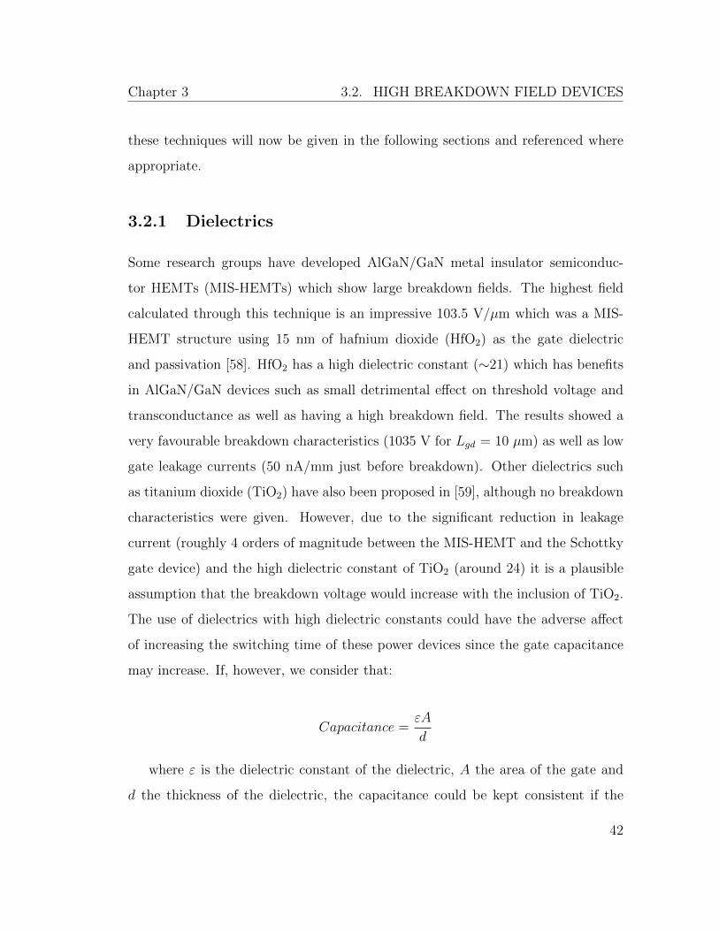
Chapter 3 3.2. HIGH BREAKDOWN FIELD DEVICES
these techniques will now be given in the following sections and referenced where
appropriate.
3.2.1 Dielectrics
Some research groups have developed AlGaN/GaN metal insulator semiconduc-
tor HEMTs (MIS-HEMTs) which show large breakdown fields. The highest field
calculated through this technique is an impressive 103.5 V/µm which was a MIS-
HEMT structure using 15 nm of hafnium dioxide (HfO2) as the gate dielectric
and passivation [58]. HfO2 has a high dielectric constant (∼21) which has benefits
in AlGaN/GaN devices such as small detrimental effect on threshold voltage and
transconductance as well as having a high breakdown field. The results showed a
very favourable breakdown characteristics (1035 V for Lgd = 10 µm) as well as low
gate leakage currents (50 nA/mm just before breakdown). Other dielectrics such
as titanium dioxide (TiO2) have also been proposed in [59], although no breakdown
characteristics were given. However, due to the significant reduction in leakage
current (roughly 4 orders of magnitude between the MIS-HEMT and the Schottky
gate device) and the high dielectric constant of TiO2 (around 24) it is a plausible
assumption that the breakdown voltage would increase with the inclusion of TiO2.
The use of dielectrics with high dielectric constants could have the adverse affect
of increasing the switching time of these power devices since the gate capacitance
may increase. If, however, we consider that:
Capacitance =εA
d
where ε is the dielectric constant of the dielectric, A the area of the gate and
d the thickness of the dielectric, the capacitance could be kept consistent if the
42

Chapter 3 3.2. HIGH BREAKDOWN FIELD DEVICES
thickness of the dielectric was increased. Reducing the gate length would reduce
the capacitance (since the overall area is decreased) and hence reduce the switching
time too.
Recently, gallium oxide (Ga2O3) was proposed for use as a dielectric beneath the
gate [60] which was deposited through RF-sputtering. A large breakdown voltage
of 2730 V was achieved for Lgd of 40 µm resulting in a breakdown field of 68.3
V/µm. Clearly a huge breakdown characteristic but a huge device as well, the
largest in Fig. 3.1. Their pulsed characteristics also showed a drain current three
times larger for the unpassivated device compared to the Ga2O3 passivated MIS-
HEMT indicating that the MIS-HEMT had trapping levels deeper than the surface
states in the unpassivated HEMT, a result which would be costly if implemented
as a high voltage power switch.
Yagi et al. [61] combined dielectrics to improve breakdown performance . They
used 50 nm of HfO2, a layer of SiO2 or Al2O3 and finally 5 nm of Si3N4 to help
improve current collapse. They achieved a breakdown field of 64.3 V/µm for a Lgd
of 28 µm. The focus was again on very large devices and no results given for smaller
gate-to-drain distances.
A smaller Lgd of 3 µm was used by Tan et al. [62] who also used a dielectric layer
of 16 nm of SiO2. The breakdown voltage reported was 145 V which translates to
a breakdown field of 48.3 V/µm. Their Schottky gate devices, with the same Lgd,
had a breakdown field of 40 V/µm.
A 3 nm Ga2O3 layer beneath the gate was grown by exposing the gate region
to an O2 plasma which gave a breakdown voltage of 87 V [63]. The corresponding
breakdown field for this device was 58 V/µm which had Lgd of 1.5 µm.
Lee et al. [64] showed that a combination of low and high-temperature Si3N4
43
Chapter 3 3.2. HIGH BREAKDOWN FIELD DEVICES
S D
GaN
AlGaN
Dielectric G
Gate Field Plate
S D
GaN
AlGaN
Dielectric G
Source Field Plate
(a) (b)
Figure 3.2: Cross section of a AlGaN/GaN HEMT showing a) Gate field plate and b) Sourcefield plate.
improved their breakdown characteristics from 120 V to 238 V (Lgd was not given
so the corresponding electric fields could not be calculated). Their devices had a
Schottky gate which were subsequently passivated with 20 nm of high temperature
Si3N4 and 180 nm of low temperature Si3N4. Their hypothesis for the increased
breakdown voltage was that charge may be trapped at the interface of the bi-layer.
This trapped charge then moderates the field at the drain-edge of the gate resulting
in a higher drain bias required for breakdown. The trapped charge, in effect, acts
very much like a field plate which will be described in the next section.
3.2.2 Field Plates
Field plates have been implemented by many research groups as a way to reduce the
impact of the electric field formed at the drain-edge of the gate. Their purpose is
to spread the electric field which forms at the gate edge, effectively reducing it and
44

Chapter 3 3.2. HIGH BREAKDOWN FIELD DEVICES
therefore increasing the drain voltage at which the device will suffer breakdown.
Their main use has been in RF AlGaN/GaN HEMT devices since the gate contact
can still be Schottky and therefore transconductance will not be compromised. Two
different types of field plates are shown in Fig 3.2 which are the gate field plate and
the source field plate.
Field plates had been previously investigated for increasing breakdown voltages
in GaAs MESFETs and were in the form of an overlapping gate structure which
had shown to be successful in [65]. In 2000 Zhang et al. [66] continued this idea for
GaN HEMTs and achieved a breakdown field of 43 V/µm. Karmalker et al. [67]
went on to develop a comprehensive account of the critical geometrical and material
variables which enable effective design of gate field plates. Their simulated results
show a potential maximum breakdown field of 134 V/µm for Lsg of 0.5 µm , Lg
of 0.4 µm and Lgd of 4.7 µm , a 20 nm n-AlGaN barrier layer and 180 nm n-GaN
buffer layer. The optimised simulated device uses 800 nm of Si3N4 beneath the field
plate and field plate length of 2.2 µm. Although their design has been optimised,
they point out that an increase in Lgd will increase the gate capacitance sufficiently
to compromise the device performance for high frequency applications.
Other groups have also investigated the effectiveness of using field plates in
AlGaN/GaN HEMTs to increase the voltage at which breakdown occurs. Okamoto
et al. [68] used a gate field plate with a recessed gate structure and achieved a
breakdown field of 80 V/µm for a Lgd of 2.5 µm. This latter structure also seemed
to improve the leakage current of the device by an order of magnitude but no reason
for this was given. Saito et al. [69] used a source connected field-plate to give an
experimental breakdown field of 60 V/µm for a Lgd of 10 µm. More recently Park
et al. [70] showed that source field plates suffer from premature breakdown if the
metal is in direct contact with the mesa side wall and so developed a mesa-first
45

Chapter 3 3.2. HIGH BREAKDOWN FIELD DEVICES
pre-passivation process to achieve a breakdown field of about 67 V/µm for a Lgd of
15 µm.
Gate field plates show the most significant improvement in breakdown fields but
come at the cost of additional parasitic capacitance which will have the adverse
effect of reducing current gain cut-off frequency fT and the power gain cut-off
frequency fMAX . To deal with this problem, Dora et al. [71] developed a HEMT
with a ‘slant-field-plate’ design. The field plate is effectively integrated into the gate
and high breakdown field of 95 V/µm was achieved for a gate-to-drain distance of
20 µm. This device utilised a Si3N4 passivation layer which was shown to effectively
reduce the dispersion even after very high voltage sweeps, however, a series of very
precise dry-etch steps are required to make this integrated field plate and therefore
making reproducibility of the fabrication process difficult.
3.2.3 Geometry
The use of a circular gate HEMT and a square-gate HEMT were proposed in [72]
and [73]. A diagram of the square-gate HEMT is shown in Fig. 3.3. The best
breakdown field achieved for this design was 54.2 V/µm for a Lgd of 12 µm whereas
the breakdown field for the circular gate HEMT was not provided. The benefit
of these types of geometrical layouts, from an electric field point of view, is that
there are no sharp corners or gate finger tips at which high electric fields between
the electrodes can occur. The structures spread out the electric field, reducing the
overall field occurring. In chapter 4 there will be simulated data to back up this
theory, albeit for slightly different layouts. These simulations were not given in the
published work and so it is important to illustrate them to understand why they
may work at higher voltages. Another benefit of this type of structure is that it is
46

Chapter 3 3.2. HIGH BREAKDOWN FIELD DEVICES
effective in eliminating the effects of traps associated with the mesa edge (since in
their design they do not require a mesa isolation stage).
Drain Source Source Drain Drain
Source Gate
Figure 3.3: Diagram of square-gate HEMT design given in [73].
3.2.4 Buffer Layer
Engineering the epilayer at the growth level is also a way in which the breakdown
voltage may be enhanced. In particular, GaN grown on Si has a large lattice
mismatch (17%) which leads to a high number of dislocations in the GaN buffer
layer. Selvaraj et al. [49] demonstrated that by growing intrinsic GaN (i-GaN)
on top of a GaN buffer layer (which consisted of multipairs of GaN/AlN (20/5
nm)), the screw dislocation density and the edge dislocation density decreased with
increasing thickness of the total GaN thickness (i.e. i-GaN plus the buffer GaN).
This translated into an increasing breakdown voltage with thickness and indeed for
a buffer thickness of 7 µm and i-GaN thickness of 2 µm a breakdown voltage of 403
V was achieved compared to only 110 V for a buffer thickness of 1 µm and i-GaN
thickness of 1 µm. Lgd was 3 µm in both cases with corresponding breakdown fields
of 36.67 V/µm and 134 V/µm. This result is the highest field plotted in Fig. 3.1.
47

Chapter 3 3.3. CONCLUSIONS
i – GaN
0.25 ~ 2 µm
25 nm AlGaN
Silicon
GaN Buffer
GaN/AlN (20/5 nm)
0.5 ~ 7 µm
Figure 3.4: Cross section of epilayer structure used by Selvaraj et al. [49]. It was shown thatwhen the i-GaN layer is grown on top of a thick buffer layer (on Si) the dislocation densitydecreases and helps to enhance the voltage at which breakdown occurs.
3.3 Conclusions
From this review it is clear that the most common approaches to engineering high
breakdown field lateral devices is to use a dielectric beneath the gate, employ field
plate structures and to a lesser extent the geometrical layout of the device and
epilayer engineering. In the traditional lateral HEMT there is clearly going to be
a limitation to the breakdown voltages due to the high electric fields at the drain-
side of the gate but it is important to try and maximise their potential as much
as possible for future commercial use. For large devices i.e. Lgd > 10µm very high
breakdown voltages can be achieved as was outlined, but this can come at the cost
of higher on-resistance (and lower drain currents) as the resistance increases with
channel length. It is therefore one of the aims of this work to engineer smaller de-
vices which have high breakdown voltages for future power electronic applications.
48

Chapter 3 3.3. CONCLUSIONS
It would also be beneficial from a commercial point of view if the devices were easily
fabricated and the fabrication processes are reproducible; analogous to the CMOS
process for Si. Work in this research will focus on how to obtain the best outputs
from AlGaN/GaN devices, using simple, well established processing techniques.
49

Chapter 4
Simulations of Electric Fields in
AlGaN/GaN HEMTs
4.1 Introduction
This chapter will describe simulations which have been carried out relevant to this
research. Device simulation and modelling are crucial in the development of any
technology allowing designers to optimise device designs and process flows before
putting them into production. This is particularly true for GaN based devices
when considering the large cost of the material. The main focus of the simulations
in this work is to give some qualitative insight into the electric fields generated in
AlGaN/GaN HEMTs under operation. It has been discussed in chapter 2 that the
peak fields at the drain-edge of the gate cause the devices to breakdown earlier than
their theoretical predictions. The results given in this chapter will show clearly how
the peaks fields can be suppressed and indeed almost completely eliminated from
the device. Some initial attention will focus on a description of the software and
50

Chapter 4 4.2. SENTAURUS TCAD SOFTWARE
other aspects of the device operation.
4.2 Sentaurus TCAD Software
The simulation tool used for the two dimensional device simulations is Sentaurus
from Synopsys which is a Technology Computer Aided Design (TCAD) software
[74]. The software is capable of simulating numerically various semiconductor ma-
terials, including Si, GaN, GaAs and so on in 1D, 2D and 3D. For the purposes of
this work, a 2D AlGaN/GaN model was obtained from the Synopsys website and
modified in order to represent the type of devices which were required. Obtaining
the model not only saved time but also ensured accurate material characteristics
such as piezoelectric polarisation were included.
The model acquired was based on an normally-off AlGaN/GaN MISFET, the
details of which can be found in [75] and [76]. The original layer structure of this
device is shown in Fig. 4.1. This type of structure is a normally-off device which
uses a piezo neutralisation technique to control the threshold voltage. As can be
seen in Fig. 4.1, there are more layers to this epi-structure than found in the more
conventional AlGaN/GaN structure i.e. the one which is to be used in this work.
Details on how the structure is modified will be given in section 4.2.2.
Sentaurus is split into different tool sets all of which have their own input files
that can be edited which enables the user to have full control over the design, the
simulating parameters and the output information. These tools include the Sentau-
rus Workbench, Sentaurus Structure Editor, Sentaurus Device, Inspect and Tecplot.
A brief description of each follows to give the reader an idea of the design/simulation
flow.
51
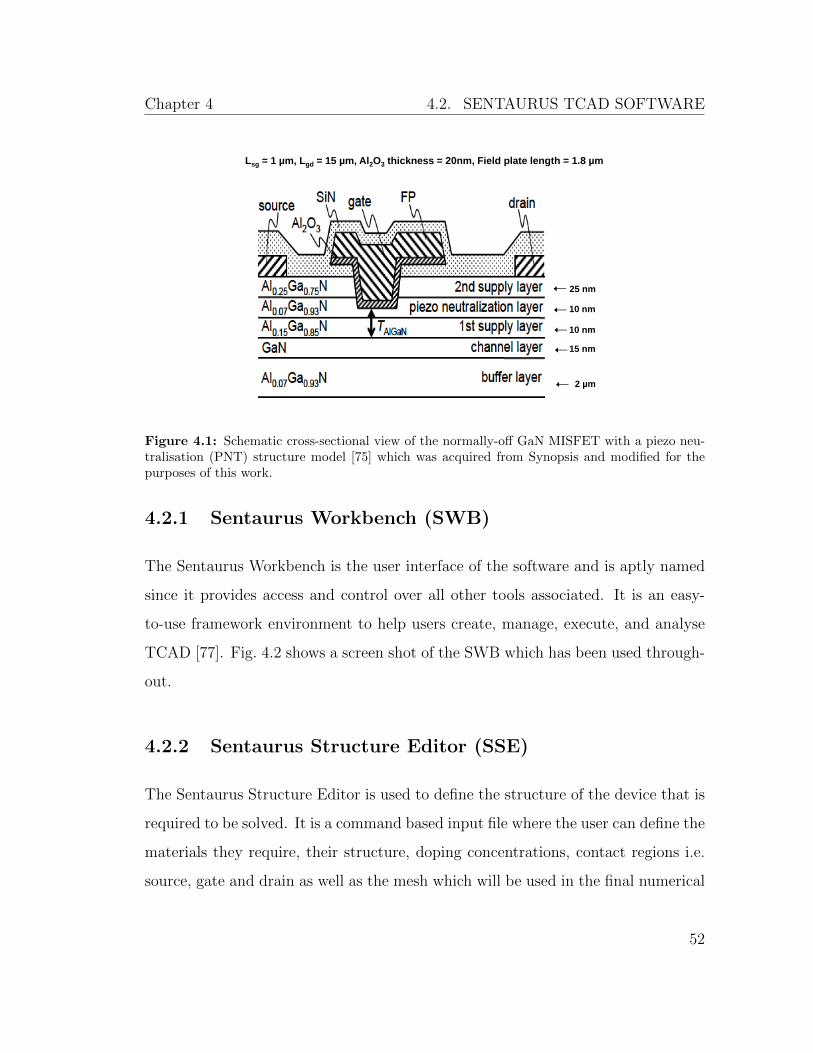
Chapter 4 4.2. SENTAURUS TCAD SOFTWARE
15 nm
2 µm
10 nm
10 nm
25 nm
Lsg = 1 µm, Lgd = 15 µm, Al2O3 thickness = 20nm, Field plate length = 1.8 µm
Figure 4.1: Schematic cross-sectional view of the normally-off GaN MISFET with a piezo neu-tralisation (PNT) structure model [75] which was acquired from Synopsis and modified for thepurposes of this work.
4.2.1 Sentaurus Workbench (SWB)
The Sentaurus Workbench is the user interface of the software and is aptly named
since it provides access and control over all other tools associated. It is an easy-
to-use framework environment to help users create, manage, execute, and analyse
TCAD [77]. Fig. 4.2 shows a screen shot of the SWB which has been used through-
out.
4.2.2 Sentaurus Structure Editor (SSE)
The Sentaurus Structure Editor is used to define the structure of the device that is
required to be solved. It is a command based input file where the user can define the
materials they require, their structure, doping concentrations, contact regions i.e.
source, gate and drain as well as the mesh which will be used in the final numerical
52
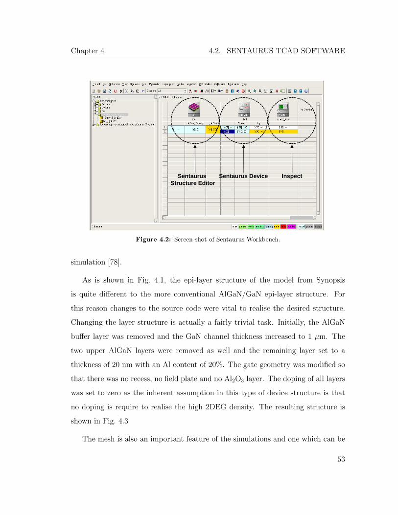
Chapter 4 4.2. SENTAURUS TCAD SOFTWARE
Sentaurus Device Sentaurus
Structure Editor
Inspect
Figure 4.2: Screen shot of Sentaurus Workbench.
simulation [78].
As is shown in Fig. 4.1, the epi-layer structure of the model from Synopsis
is quite different to the more conventional AlGaN/GaN epi-layer structure. For
this reason changes to the source code were vital to realise the desired structure.
Changing the layer structure is actually a fairly trivial task. Initially, the AlGaN
buffer layer was removed and the GaN channel thickness increased to 1 µm. The
two upper AlGaN layers were removed as well and the remaining layer set to a
thickness of 20 nm with an Al content of 20%. The gate geometry was modified so
that there was no recess, no field plate and no Al2O3 layer. The doping of all layers
was set to zero as the inherent assumption in this type of device structure is that
no doping is require to realise the high 2DEG density. The resulting structure is
shown in Fig. 4.3
The mesh is also an important feature of the simulations and one which can be
53

Chapter 4 4.2. SENTAURUS TCAD SOFTWARE
1 μm GaN
20 nm Al0.20Ga0.80N S
G
D
Highly doped region
beneath contact to imitate
GaN Ohmic contacts
Lsg = 1.5 µm Lg = 2 µm Lgd = 3 µm
Highly doped region
beneath contact to imitate
GaN Ohmic contacts
Figure 4.3: Diagram of modified model in Sentaurus used in this work.
modified in the SSE. A dense mesh will improve on accuracy of the results and is
used in regions of particular interest i.e. where large field variations are expected
and a less dense mesh may be used in the bulk of the material since no significant
spatial variation of the field is expected. The mesh was, in the main, unaltered as
there was already a high mesh density around the gate area where the high electric
field analysis was being carried out.
4.2.3 Sentaurus Device (SD)
Sentaurus Device allows the user to define certain parameters for the simulation to
be carried out. It is split into several sections; Electrode, Physics, Maths, Plot and
Solve. A brief description of each follows [79]:
Electrode The user can define the type of electrode required for each contact
i.e. Ohmic or Schottky. Additionally the workfunctions of the metals used can be
defined and the initial voltage which is to be applied for the simulation. For the
54

Chapter 4 4.2. SENTAURUS TCAD SOFTWARE
structure used in this research, Schottky contacts are used in the source and drain
regions for robustness [76]. Electron tunnelling is turned on and the electron tun-
nelling mass is made to be arbitrarily small so that the contact is essentially Ohmic.
These settings result in a better convergence rate than using Ohmic contacts. A
high doping concentration is also used around the source and drain regions to emu-
late n-type like doping which occurs in real life devices after annealing the contacts
[80].
Physics This is where the physical models can be defined to be used in the
simulation i.e. mobility, trapping, strain, tunnelling, polarisations. Polarisations in
GaN structures was detailed in section 2.3.2. It is these strong polarisations that
create an interface charge between the AlGaN and the GaN and these values are
computed automatically using the built in strain piezoelectric model in Sentaurus
Device. The models were already included in the source code and were untouched
throughout the project.
At the time of writing, access to Sentaurus was unavailable and so a full de-
scription of these models is unfortunately unable to be included.
Maths Here Sentaurus Device solves the transport equations self-consistently in
an iterative manner. For each iteration an error is calculated and Sentaurus Device
attempts to converge on a solution that has an acceptably small error.
Plot Here is where the quantities which are calculated through the simulation
can be output to a file for each mesh point. An example would be to specify that
you want the conduction band energy (ConductionBand) or the electron mobility
(eMobility) output for the simulated device.
55

Chapter 4 4.2. SENTAURUS TCAD SOFTWARE
Solve The Solve section defines what equations are required to be solved for the
simulations. The equations used here were Poisson’s equations and the current con-
tinuity for electrons and holes. The work here is very much focussed on the electric
fields within the devices and so for this reason Poisson’s equation for electrostatic
potential must be solved. This is because all mobile charges (electrons and holes)
and immobile charges (ionised dopants or traps) play a key role in determining the
electrostatic potential. Poisson’s equation is:
∇(ε∇.ψ) = −q(p− n+ND −NA)− ρtrap (4.1)
where ψ is the electrostatic potential, ε is the dielectric constant, q is the ele-
mentary electronic charge, n and p are the electron and hole densities, ND is the
concentration of ionised donor, NA is the concentration of ionised acceptors and
ρtrap is the charge density contributed by traps and fixed charges.
The transport of the electrons and holes must also be considered when modelling
semiconductor devices. Sentaurus supports four different types of transport models
depending on the accuracy required. These are Drift-Diffusion, Hydrodynamic,
Thermionic and Monte-Carlo. They can all be written in the form of continuity
equations, which describe charge conservation:
∇.−→J n = qRnet + q
∂n
∂t(4.2)
−∇.−→J p = qRnet + q
∂n
∂t(4.3)
where Rnet is the net recombination rate,−→J n is the electron current density,
−→J p is the hole current density. The Drift-Diffusion model is the default one used
56

Chapter 4 4.2. SENTAURUS TCAD SOFTWARE
in Sentaurus and does not take into account thermal effects or impact ionisation in
the devices. Since the devices under investigation were relatively large (i.e. several
microns in length) and required high biasing voltages for the analysis, this model
is sufficient since it converges much quicker than the others. For more detailed
simulations involving carrier transport one of the other models may be used but
come at the cost of large computational time.
Other material parameters such as the band gap, electron affinity, electron/hole
mass etc. can also be altered in Sentaurus Device. As with the models outlined
in the Physics section, the inaccessibility to Sentaurus means that the values of
these parameters cannot be included, however, it should be noted that these were
untouched due the model already having parameters set.
4.2.4 Tecplot and Inspect
These are the tools used to visualise the device and the simulated results, includ-
ing I-V characteristics. Output characteristics of the device such as electric field,
electrostatic potential, conduction and valence band energies and electron densities
as well as many others may be inspected. Some diagrams from Tecplot will be in-
cluded throughout this chapter which give an instant visual insight into the device
operation. From these diagrams data can be extracted in slices or as single points
and plotted to give more information as will be given.
57
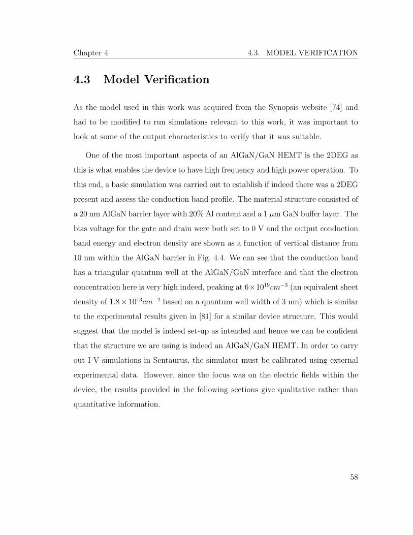
Chapter 4 4.3. MODEL VERIFICATION
4.3 Model Verification
As the model used in this work was acquired from the Synopsis website [74] and
had to be modified to run simulations relevant to this work, it was important to
look at some of the output characteristics to verify that it was suitable.
One of the most important aspects of an AlGaN/GaN HEMT is the 2DEG as
this is what enables the device to have high frequency and high power operation. To
this end, a basic simulation was carried out to establish if indeed there was a 2DEG
present and assess the conduction band profile. The material structure consisted of
a 20 nm AlGaN barrier layer with 20% Al content and a 1 µm GaN buffer layer. The
bias voltage for the gate and drain were both set to 0 V and the output conduction
band energy and electron density are shown as a function of vertical distance from
10 nm within the AlGaN barrier in Fig. 4.4. We can see that the conduction band
has a triangular quantum well at the AlGaN/GaN interface and that the electron
concentration here is very high indeed, peaking at 6×1019cm−3 (an equivalent sheet
density of 1.8× 1013cm−2 based on a quantum well width of 3 nm) which is similar
to the experimental results given in [81] for a similar device structure. This would
suggest that the model is indeed set-up as intended and hence we can be confident
that the structure we are using is indeed an AlGaN/GaN HEMT. In order to carry
out I-V simulations in Sentaurus, the simulator must be calibrated using external
experimental data. However, since the focus was on the electric fields within the
device, the results provided in the following sections give qualitative rather than
quantitative information.
58
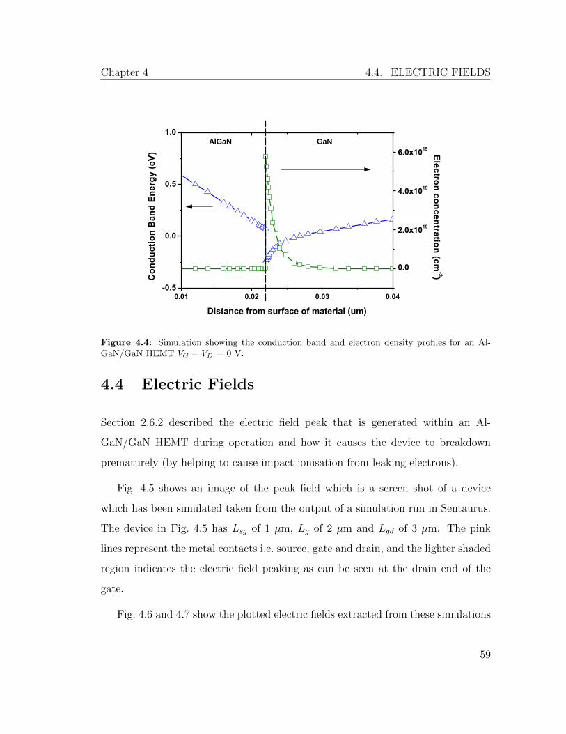
Chapter 4 4.4. ELECTRIC FIELDS
0.01 0.02 0.03 0.04
-0.5
0.0
0.5
1.0
Distance from surface of material (um)
Co
nd
uc
tio
n B
an
d E
ne
rgy
(e
V)
0.0
2.0x10¹⁹
4.0x10¹⁹
6.0x10¹⁹
Ele
ctro
n c
on
ce
ntra
tion
(cm
-3)
AlGaN GaN
Figure 4.4: Simulation showing the conduction band and electron density profiles for an Al-GaN/GaN HEMT VG = VD = 0 V.
4.4 Electric Fields
Section 2.6.2 described the electric field peak that is generated within an Al-
GaN/GaN HEMT during operation and how it causes the device to breakdown
prematurely (by helping to cause impact ionisation from leaking electrons).
Fig. 4.5 shows an image of the peak field which is a screen shot of a device
which has been simulated taken from the output of a simulation run in Sentaurus.
The device in Fig. 4.5 has Lsg of 1 µm, Lg of 2 µm and Lgd of 3 µm. The pink
lines represent the metal contacts i.e. source, gate and drain, and the lighter shaded
region indicates the electric field peaking as can be seen at the drain end of the
gate.
Fig. 4.6 and 4.7 show the plotted electric fields extracted from these simulations
59

Chapter 4 4.4. ELECTRIC FIELDS
for devices with a drain bias - Fig. 4.6 is for VD = 5 V and Fig. 4.7 is for VD = 10
V. The field components plotted (which are extracted from Tecplot) are the lateral
Ex, vertical Ey and absolute Eabs i.e.√E2
x + E2y . Fig. 4.7 shows a clear increase in
the overall electric field compared to Fig. 4.6, which will continue to increase with
the drain bias. It is clear from these diagrams that the lateral field Ex contributes
the largest portion to the overall field and is clearly the one which should be paid
most attention whilst designing HEMTs for high power applications where very
large voltages will be applied to the drain. It is worth noting that the electric field
profiles follow that of the theory given by Somerville et al. [47] i.e. strongly peaked
at the drain edge of the gate, which again confirms the validity of the model.
Light region
indicating
electric field
Gate
So
urc
e
Dra
in
Figure 4.5: Image from Tecplot showing the output electric field of an AlGaN/GaN device withhigh drain bias. It can be seen that the electric field peaks strongly at the drain side of the gate.This diagram is for illustrative purposes only.
60

Chapter 4 4.4. ELECTRIC FIELDS
1 2 3 4 5 6
-1
0
1
2
Ele
ctr
ic F
ield
(M
V/c
m)
Cross section along 2DEG (um)
Absolute Field E(abs)
Vertical Field (Ey)
Lateral Field (Ex)
Figure 4.6: Electric fields for VD = 5 V and VG = -4 V. Device structure same as that in Fig.4.5.
1 2 3 4 5 6
-1
0
1
2
Ele
ctr
ic F
ield
(M
V/c
m)
Cross section along 2DEG (um)
Absolute Field E(abs)
Vertical Field (Ey)
Lateral Field (Ex)
Figure 4.7: Electric fields for VD = 10 V and VG = -4 V. Device structure same as that in Fig.4.5.
61

Chapter 4 4.5. MIS-HEMTS
4.5 MIS-HEMTs
In Section 3.2.1 it was shown that there were some research groups who have used
dielectric layers beneath the gate to increase the breakdown voltage. Here we show
the impact that a dielectric layer can have on the electric field whilst under high
biasing. Fig. 4.8 shows the simulated results for two devices:
1. A HEMT with a Schottky gate and
2. A MIS-HEMT with 10 nm of Si3N4 beneath the gate.
The device structure used for these simulations consisted of a 20 nm AlGaN
barrier layer, a 2 µm GaN buffer layer, Lsg of 1.5 µm, Lg of 2 µm and Lgd of 3 µm.
1 2 3 4 5 6 70
1
2
3
4
5
Ele
ctr
ic F
ield
(M
V/c
m)
VDS
(V)
SG HEMT VG = -4 V
MIS-HEMT VG= -6 V
LSG = 1.5 μm LG = 2 μm LGD = 3 μm
Figure 4.8: Plotted electric fields for Schottky Gate and 10 nm Si3N4 MIS-HEMT. Vd is 20 Vin both cases and Vg is -4 V and -6 V respectively. The reduced electric field in the barrier regionis due to some of the voltage being dropped across the dielectric.
62

Chapter 4 4.6. GATE OVERLAPPING HEMT FOR RF OPERATION
Both devices were biased with 20 V on the drain and gate voltages of -4 V for the
Schottky gate and -6 V for the MIS-HEMT. These gate voltage values were chosen
because during breakdown measurements the device is pinched off and so based on
previous experience in characterising such device structures, -4 V and -6 V were
chosen.
From the graph we can see that the overall electric field in the barrier region
is reduced with the inclusion of the dielectric. This is due to the gate contact
being slightly further away than it is in the Schottky gate HEMT and some of the
induced voltage will be dropped across the dielectric. This implies that a higher
drain voltage will be required to initiate impact ionisation and cause the device to
breakdown. For high voltage devices this method of increasing the breakdown field
is and should be employed. The choice of dielectric is the next question and for
the purposes of this work Si3N4 was used as it is widely accepted that it increases
carrier concentration in the 2DEG and so improves devices power performance
[82]. However, as shown in [58], HfO2 has proved to be a good choice both for
breakdown and current collapse. This trend of suppressing the field will continue
with increasing thickness of the dielectric layer but this will lead to other problems
such as reduced transconductance (important for RF devices) and an increase in
threshold voltage (depending on the dielectric constant of the insulating material).
For D-mode devices this is an undesirable effect since the threshold would become
more negative and ‘pinching - off’ the device would require a larger negative voltage.
4.6 Gate Overlapping HEMT for RF Operation
Almost all lateral AlGaN/GaN HEMTs in the literature use the traditional MES-
FET type structure with the gate sitting in between the source and drain with
63
Chapter 4 4.6. GATE OVERLAPPING HEMT FOR RF OPERATION
a source-gate and drain-gate separation (refer to Fig 1.3). In a MESFET, no in-
sulating layer is used and so the gaps between the gate and the source/drain are
necessary to avoid a short circuit. In traditional MOSFETs i.e. Si transistors with
thermally grown SiO2, the gate covers the whole channel and slightly overlaps the
source/drain regions and is known as the self-aligned gate structure. In MOSFETs
this has the benefit of reducing parasitic capacitances which leads to faster de-
vices. This type of structure has not been used for an AlGaN/GaN HEMT device
previously.
Fig. 4.9 shows the simulated electric field of the device and Fig. 4.10 shows a
cross section of the total electric field which is taken along the 2DEG for a device
which has no gate and a drain bias of 5 V plus the device which has the gate
overlapping the source and the drain (by 50 nm in these simulations). The reason
for including the plot of the device with no gate is to show that there are large
peaks at the edge of the source and drain contacts regardless of whether the gate is
present or not. These fields, however, are associated with the metal contacts and
not the material. It can be observed from the screen shot of the simulated device
in Fig. 4.9 that there are no electric field peaks in the channel. This is confirmed
in Fig. 4.10 where the cross section along the 2DEG shows that the field is almost
uniform along the channel and that the electric field peak observed in the more
traditional AlGaN/GaN lateral HEMT is eliminated.
This device structure has shown to eliminate the peak electric field at the drain
edge of the gate but it has not taken account of the fact the gate edge is now in very
close proximity to the drain, separated by only the insulator. This now means that
the breakdown voltage of the device would be determined by the voltage that it
takes to cause breakdown within the insulator, which would depend on its dielectric
constant and its thickness. The thickness of the dielectric in this case is only 10 nm
64

Chapter 4 4.6. GATE OVERLAPPING HEMT FOR RF OPERATION
AlGaN
GaN
Dielectric
Gate
So
urc
e D
rain
Figure 4.9: Screen shot of simulation from Sentaurus of gate overlapping HEMT. The gatecovers the entire channel and no large electric field peak can be observed.
and a further increase of this would have a diminishing effect on other aspects of
the devices’ performance i.e. transconductance. So although the problem with the
peak field has been eliminated, the devices’ performance for high breakdown, in all
likelihood, would be far inferior to the device structures discussed in section 4.5.
Gate leakage current due to lateral tunnelling may be eliminated as well as
current collapse with this design structure which, as was mentioned in Section 2.5.2,
is due to a ‘virtual gate’ building up on the exposed areas of the surface - there
are no exposed areas in this device’s design. However, as AlGaN/GaN devices are
being targeted for high power applications is extremely unlikely that these benefits
would outweigh the very low breakdown voltages that are inevitable (experimental
work will show this in chapter 7).
65

Chapter 4 4.7. CONCLUSIONS
1 2 30
1
2
3
4
5
6
7
8
Ele
ctr
ic F
ield
(M
V/c
m)
Cross section along 2DEG (um)
Device with no gate VD = 5V
Device with gate over entire channel VD = 10V
G
S
Dielectric
D
AlGaN
GaN
2DEG
Figure 4.10: Resulting electric fields along 2DEG for HEMT where the gate covers the entirechannel and overlaps the drain and source (by 50 nm in these simulations).
4.7 Conclusions
This chapter described simulated results that have given an insight into AlGaN/GaN
device operation at large drain biases, a realistic reflection on a real life scenario.
These insights gave us the information we required to try and resolve the issues
which cause AlGaN/GaN HEMTs to fall short of their potential breakdown field
of around 300 V/µm. The inclusion of the dielectric beneath the gate clearly sup-
presses the field generated at the drain-edge of the gate and although a thicker
dielectric would have a greater effect this would make the device difficult to switch
off. The device in which the gate covers the entire channel (similar to the self-
aligned Si-MOSFET device) showed that the peak field in the channel could be
eliminated but did not take account of the gate edge being so close to the drain
contact that the breakdown would actually be determined by the insulator breaking
66

Chapter 4 4.7. CONCLUSIONS
down. This device may eventually be suitable for low voltage applications, but it
is unlikely that it would be able to replace low voltage transistors based on Si or
GaAs.
67

Chapter 5
Fabrication and Characterisation
of AlGaN/GaN HEMT Unit Cells
5.1 Introduction
This chapter will outline the types of devices used throughout the course of this
research. These can be coarsely split into two categories; DC (direct current) and
RF (radio frequency). For the purposes of research, ‘unit cells’ of larger device
are fabricated. This is to save on space on the material and also provide quick
characterisation results. The layout for each type of device is quite different but the
basic fabrication principles for both follow a very similar process. These processes
will be outlined and detailed descriptions given.
68
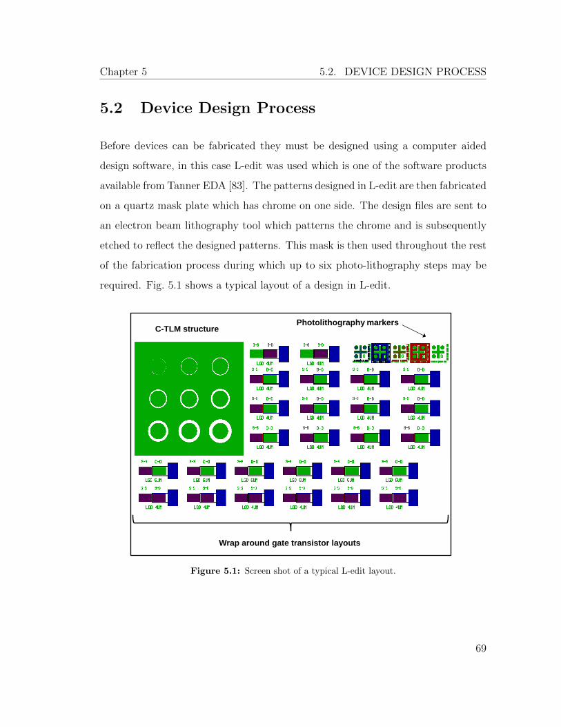
Chapter 5 5.2. DEVICE DESIGN PROCESS
5.2 Device Design Process
Before devices can be fabricated they must be designed using a computer aided
design software, in this case L-edit was used which is one of the software products
available from Tanner EDA [83]. The patterns designed in L-edit are then fabricated
on a quartz mask plate which has chrome on one side. The design files are sent to
an electron beam lithography tool which patterns the chrome and is subsequently
etched to reflect the designed patterns. This mask is then used throughout the rest
of the fabrication process during which up to six photo-lithography steps may be
required. Fig. 5.1 shows a typical layout of a design in L-edit.
Photolithography markers
Wrap around gate transistor layouts
C-TLM structure
Figure 5.1: Screen shot of a typical L-edit layout.
69

Chapter 5 5.2. DEVICE DESIGN PROCESS
5.2.1 Designing Device Layouts
DC Devices
DC devices are those which have a gate and drain bias applied to them directly and
output characteristics such as IDS −VDS, gate leakage IG−VGD, transconductance
gm and breakdown voltages VBR can all be measured. At Glasgow University,
the measurements are carried out using a semi-automatic probe station which is
connected to an Agilent B1500A semiconductor parameter analyser (SPA) [84].
The probes are carefully placed onto the contacts and the DC biases are set from
the SPA where the resulting output characteristics are also displayed.
For a fast turnaround in device production a wrap-around gate structure as
shown in Fig 5.2 may be employed in which the gate encompasses the drain region
and therefore a mesa isolation etch step is not required. These types of devices
have been made throughout the course of this research for device optimisation and
results. Other structures have also been made throughout for which detail will be
given where necessary.
When considering devices for high voltage characterisation, the bond pads must
be carefully considered. These must be able to make a good electrical connection
to the probes which will be used but must also be large enough so that the probes
can easily contact them. For high voltage breakdown measurements it is desirable
to have the bond pads quite far apart from each other since flash over between the
probes may occur due to the breakdown field of air being lower than that of GaN
(30 kV/cm compared to 3 MV/cm).
70

Chapter 5 5.2. DEVICE DESIGN PROCESS
Source Drain Gate
Figure 5.2: Wrap around gate HEMT.
RF Devices
RF devices are those which are used for microwave applications such as power
amplifiers. Small signal scattering parameters on a vector network analyser can
be measured to assess how much gain the device gives at a particular frequency.
Record current gain cut-off frequencies fT of 194 GHz with a 0.045 µm gate length
[85] and maximum oscillation frequency fMAX of 300 GHz with a gate length of 0.06
µm [86] have been demonstrated, indicating the potential of AlGaN/GaN material.
Previously here at Glasgow University, small RF devices with gate lengths of 200 nm
have been fabricated on AlN/GaN material displaying fT of 50 GHz and fMAX of 40
GHz [16]. These latter devices also demonstrated high drain currents of 1.5 A/mm
due to the all binary AlN barrier layer which provides higher 2DEG concentrations.
For the most part, AlGaN/GaN HEMTs are geared towards X-band applications
i.e. 8 - 12 GHz, frequencies at which high output power densities of 20.9 W/mm
have been achieved with gate lengths of 0.65 µm [87] and 16.7 W/mm with a gate
length of 0.7 µm [88] (this latter result was demonstrated on N-polar AlGaN/GaN
71

Chapter 5 5.3. DEVICE PROCESSING
Drain
Source
Source
Gate fingers
Bond pads
Bond pads
Mesa
Figure 5.3: Typical layout of unit cell of RF device which has two gate fingers.
material).
The layout of a typical RF transistor unit cell for research purposes consists
of two gate fingers and is shown in Fig. 5.3 (when implemented for amplifiers etc.
the number of fingers will increase to increase the output current/power). When
fabricating many RF devices on the same sample of material, a mesa isolation step
is required to electrically isolate them from one another on the sample. Details on
mesa isolation will be given in section 5.3.4.
5.3 Device Processing
Device fabrication was carried out in the James Watt Nanofabrication Centre
(JWNC), University of Glasgow. This centre was opened in 2006 and houses all of
university’s micro and nanofabrication facilities. The following sections will outline
the processes required to take an epitaxially grown wafer through to the completed
72

Chapter 5 5.3. DEVICE PROCESSING
GaN
AlGaN
GaN
AlGaN
Photoresist
GaN
AlGaN
GaN
AlGaN
GaN
AlGaN
GaN
AlGaN
Undercut profile
(a)
(b)
(c)
(d)
(e)
(f)
Figure 5.4: Device process (a) Sample has been cleaned and is ready to be processed (b)Photoresist is spun onto sample (c) Sample has been soaked in developer solution and is nowbeing subjected to UV light. The black boxes on top of the photoresist indicate the mask platein contact with the sample, protecting areas which do no require to be patterned (d) Photoresistis developed and shows an undercut profile which will benefit the metal lift-off process (e) Thesample is then metallised in the electron beam evaporator (f) Finally the sample is immersed inwarm acetone to remove the photoresist and leave behind only the metal which was evaporateddirectly onto the material.
73

Chapter 5 5.3. DEVICE PROCESSING
working device stage. Fig. 5.4 shows the process flow for photolithography and
metallisation and should be referred to when reading the following sections.
5.3.1 Sample Structure and Preparation
The primary material used throughout this project was based on the AlGaN/GaN
structure which was shown in Fig 1.3. Differences such as the inclusion or absence
of a GaN cap layer, the AlGaN barrier thickness and Al content were common and
details will be addressed along with device results in later chapters.
AlGaN/GaN wafers were grown with a 2-inch diameter which was then scribed
and cleaved into smaller samples, usually 1 cm x 1 cm, due to its significant expense.
The samples are then initially immersed in a glass beaker of acetone and placed
into an ultra-sonic bath for 15 minutes. The acetone is then removed by placing
the sample into isopropyl alcohol for a few minutes. This procedure ensures that
any debris from the wafer cleaving or any other contaminants are removed.
5.3.2 Lithography
Semiconductor fabrication relies on lithography to define very small features onto
the material which is being used. Primarily, lithography is used so that metal
contacts can be defined but it is also used for etching as well. During the course of
this research, photolithography was used predominantly due to its low cost and also
being a manual process which enables faster device production. It does, however,
limit the size of the features which may be processed to around 1 µm due to the
wavelength of the lamp source used (an ultraviolet (UV) lamp with a wavelength
of 365 nm in this case). This resolution is acceptable for devices made for proof
74

Chapter 5 5.3. DEVICE PROCESSING
of concept but for much smaller features then electron beam lithography must be
used.
Photolithography requires several steps which are outlined below and had been
previously been developed for GaN development in the JWNC:
1. Sample preparation as outlined in the previous section.
2. Coating the sample with photoresist. The Shipley S1800 positive photoresists
were primarily used throughout. S1818 (roughly 1.8 µm thick when spun
at 4000 rpm) was used for large features such as Ohmic contacts and S1805
(roughly 0.5 µm thick) for smaller features such as gate contacts. The coating
of the sample with resist is done using a resist spinner in the JWNC.
3. The resist is baked after spinning at 65C for 2 minutes. This step promotes
resist adhesion to the sample as well as removing unwanted solvents.
4. The final step prior the exposure to UV light is to soak the sample in a
solution of Shipley Microposit Developer Concentrate and water at a ratio of
1:1 for one minute. This is said to harden the surface of the resist and ensure
a good undercut (once exposed) which is required for a good metal lift-off
profile (see Fig. 5.4.)
5. The sample can then be exposed to the UV light with the mask plate, as
described in section 5.2, protecting areas which do not require to be metallised
or etched. For S1818 a 5 second exposure is required and for S1805, 3 seconds.
6. The exposed areas are then developed out by placing the sample in the same
solution as used in step 4 and agitating it for 75 seconds. A thorough rinse
in water follows.
75
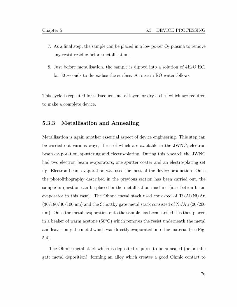
Chapter 5 5.3. DEVICE PROCESSING
7. As a final step, the sample can be placed in a low power O2 plasma to remove
any resist residue before metallisation.
8. Just before metallisation, the sample is dipped into a solution of 4H2O:HCl
for 30 seconds to de-oxidise the surface. A rinse in RO water follows.
This cycle is repeated for subsequent metal layers or dry etches which are required
to make a complete device.
5.3.3 Metallisation and Annealing
Metallisation is again another essential aspect of device engineering. This step can
be carried out various ways, three of which are available in the JWNC; electron
beam evaporation, sputtering and electro-plating. During this research the JWNC
had two electron beam evaporators, one sputter coater and an electro-plating set
up. Electron beam evaporation was used for most of the device production. Once
the photolithography described in the previous section has been carried out, the
sample in question can be placed in the metallisation machine (an electron beam
evaporator in this case). The Ohmic metal stack used consisted of Ti/Al/Ni/Au
(30/180/40/100 nm) and the Schottky gate metal stack consisted of Ni/Au (20/200
nm). Once the metal evaporation onto the sample has been carried it is then placed
in a beaker of warm acetone (50C) which removes the resist underneath the metal
and leaves only the metal which was directly evaporated onto the material (see Fig.
5.4).
The Ohmic metal stack which is deposited requires to be annealed (before the
gate metal deposition), forming an alloy which creates a good Ohmic contact to
76
Chapter 5 5.3. DEVICE PROCESSING
the material. This step is carried out by rapid thermal annealing (RTA) in N2 at
800C for 30 seconds.
5.3.4 Dry Etch
Overview
Etching is a crucial process in most semiconductor device fabrication. Due to the
difficulty in wet etching 0001 GaN [89], much attention has been focussed on dry
etch processes using inductively coupled plasma (ICP), electron cyclotron resonance
(ECR) or reactive ion etching (RIE) techniques [90]. ICP and ECR techniques have
shown to be the most effective way of etching these materials [90] although RIE
has also been used extensively. ICP and RIE tools are illustrated in Fig. 5.5. The
main difference between the two etching techniques is that in the RIE tool has a
single RF plasma source which determines both ion density and energy whereas in
the ICP tool has separate RF and ICP generators allowing for separate control over
ion energy and ion density, enabling high process flexibility [91]. During the course
of this research the JWNC invested in an ICP dry etch tool (ICP 180 from Oxford
Instruments) which was used for the bulk of the dry-etching work used here.
Various gases have been investigated over the years when dry-etching GaN (or
AlGaN), most commonly Cl2, BCl3, Ar and SiCl4. Usually a combination of these
gases is used, for example Cl2 with BCl3, but Cl2 on its own has shown to be
effective for low damage shallow etches [92]. The following two section will details
the processes used for this work for deep mesa isolation etching and for shallow,
low damage etches.
77
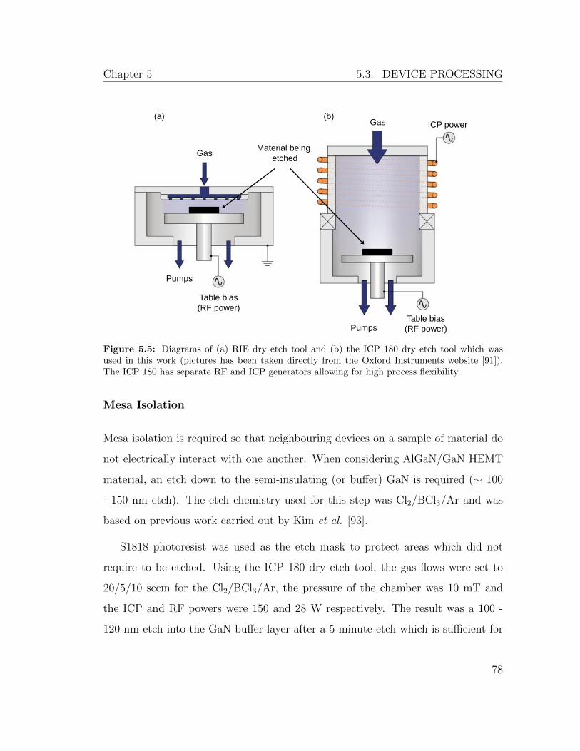
Chapter 5 5.3. DEVICE PROCESSING
Table bias
(RF power)
ICP power
Pumps
Gas
Table bias
(RF power)
(a) (b)
Material being
etched Gas
Pumps
Figure 5.5: Diagrams of (a) RIE dry etch tool and (b) the ICP 180 dry etch tool which wasused in this work (pictures has been taken directly from the Oxford Instruments website [91]).The ICP 180 has separate RF and ICP generators allowing for high process flexibility.
Mesa Isolation
Mesa isolation is required so that neighbouring devices on a sample of material do
not electrically interact with one another. When considering AlGaN/GaN HEMT
material, an etch down to the semi-insulating (or buffer) GaN is required (∼ 100
- 150 nm etch). The etch chemistry used for this step was Cl2/BCl3/Ar and was
based on previous work carried out by Kim et al. [93].
S1818 photoresist was used as the etch mask to protect areas which did not
require to be etched. Using the ICP 180 dry etch tool, the gas flows were set to
20/5/10 sccm for the Cl2/BCl3/Ar, the pressure of the chamber was 10 mT and
the ICP and RF powers were 150 and 28 W respectively. The result was a 100 -
120 nm etch into the GaN buffer layer after a 5 minute etch which is sufficient for
78

Chapter 5 5.3. DEVICE PROCESSING
device isolation.
Shallow Etching
For the Schottky drain contacts (which will be described and used in chapters 6,
7 and 8) a shallow etch into the AlGaN barrier layer is necessary to reduce the
on-resistance and turn on voltage of the completed device [34]. This type of etch
is far more challenging than the mesa isolation step since it is very shallow (∼ 10
- 12 nm) which is difficult to measure accurately. Low power Cl2 etches have been
used previously for such etching [92, 94, 95], however, all these etches used RIE
and not the ICP technique which was going to be used here. From these papers we
established initial gas flows and pressures which we wanted to use which allowed
us to focus on the ICP and RF powers in order to achieve a low damage, slow
controllable etch rate.
Cl2 and BCl3 with flow rates of 10 sccm and 5 sccm respectively were chosen
(the Cl2 being the main etching agent) with a chamber pressure of 20 mT and a
table temperature of 30C. It was a requirement that this etch was very low damage
as it would be used for creating a Schottky contact eventually. In order to do this,
it was desirable to keep the RF power low and hence the energy of the gas ions low.
The material used throughout this development consisted of a 25 nm AlGaN barrier
layer followed by a 1.4 µm GaN buffer layer and the etch times were 5 minutes.
The etched depths were measured using atomic force microscopy (AFM). Fig. 5.6
shows the resulting etch rates against DC bias (with the ICP and RF powers used
in each case included with each data point). Generally, the etch rate decreases with
decreasing DC bias which is a result of how the ICP and RF power sources are set.
An etch rate of about 5 nm/min was found at a DC bias of - 70 V with ICP power
= 100 W and RF power = 13 W. To verify this, further tests were carried out
79

Chapter 5 5.3. DEVICE PROCESSING
0
5
10
15
20
25
30
35
40
45
-225 -110 -70 -25
Etch
Rat
e (
nm
/min
)
DC Bias (V)
ICP=90W
RF=50W
ICP=45W
RF=30W
ICP=100W
RF=13W
ICP=30W
RF=15W
Figure 5.6: Plot showing how the etch depth is affected by the DC bias and the correspondingetch rate for AlGaN/GaN material. The corresponding ICP and RF powers (which are set by theuser) are included with each data point.
for varying lengths of time, the results of which are shown in Fig. 5.7. From this
graph we can see that the etch rate follows an almost linear line for etch times up
to 10 minutes. Fig. 5.8 shows an AFM step height for an etch carried out for 3
minutes at - 70 V DC bias. We can see from this trace that that the etch depth is
about 10 nm and the surface roughness of the etched and non etched material is
similar, indicating the low damage quality of the etch. A root mean square surface
roughness of 0.1 - 0.2 nm was measured for both etched and non etched regions.
The trace in Fig. 5.8 should be approached with some caution though as the
depth of the measurement is very small (low nm range) and all measurements are
subject to systematic errors (an estimated value of 5% here). The reasons being
that the AFM tip is very sensitive and so any disturbance i.e. movement within the
80

Chapter 5 5.3. DEVICE PROCESSING
0
10
20
30
40
50
0 2 4 6 8 10 12
Etc
h D
ep
th (
nm
)
Time (minutes)
Figure 5.7: Shallow etch depths for AlGaN/GaN epilayer at bias voltage of -70 V. The rate isroughly 4 - 5 nm/min.
room in which the measurement is taking place or change in atmospheric conditions
could alter the final outcome of the measurement. The condition of the AFM tool
itself may not be as is intended (e.g. a calibration of the tool may not have been
carried out for some days causing drift in the measurements) and therefore the
measurements taken again might not be the actual depth of the measured regions.
A combination of these factors means that if the measurements were repeated after
a period of time, a slightly different depth might be measured. Fig. 5.8 also shows
dotted lines which represent the average depth measured in this case but there is an
uncertainty of roughly 1 nm associated with the placement of these lines which, in
combination with the systematic error of 5%, gives an total estimated uncertainty
of 1.5 nm or 15%. So although the trace in Fig. 5.8 showed an average etch depth
81

Chapter 5 5.4. SUMMARY
32.521.510.50
12
10
8
6
4
2
0
X[µm]
Z[n
m]
~ 10 nm
Figure 5.8: AFM trace of step height of 3 minute etch with DC bias of -70 V showing a stepheight of 10 nm with similar surface roughness for etched and non etched regions.
of 10 nm, more data would be required over a period of time where the mean value
plus the standard deviation about this could be determined and give more meaning
to this measurement (this would also therefore depend on the etch tools as well as
their conditions may well also change over time).
5.4 Summary
This chapter has given an oversight into how AlGaN/GaN HEMTs have been pro-
duced throughout the course of this research. Although the techniques described are
not unique to AlGaN/GaN, they may have been modified and further investigated
(the dry-etching for example) to fulfil the requirements. The next chapters will go
82

Chapter 5 5.4. SUMMARY
onto describe fabricated devices which will make use of all the aspects described
here and will only refer to them briefly when describing individual fabrication runs.
83

Chapter 6
High Breakdown Voltage
AlGaN/GaN HEMTs and
MIS-HEMTs
6.1 Introduction
This chapter will give experimental results for the simulated data given in section
4.5. The results in section 4.5 showed that with the inclusion of Si3N4 beneath
the gate, the electric field at the drain-side of the gate is suppressed for the same
drain bias as the Schottky gate devices. It was assumed that the consequence
of this would be a higher voltage required for device breakdown. This chapter is
split into three sections: the first section focuses on the breakdown analysis between
Schottky gate and MIS-HEMT devices; the second part will further try and improve
on these devices by incorporating a Schottky drain contact and finally an analysis
of the quality of the Si3N4 used as the gate dielectric will be given.
84

Chapter 6 6.2. HEMT AND MIS-HEMT BREAKDOWN VOLTAGES
6.2 HEMT and MIS-HEMT breakdown voltages
6.2.1 Fabrication
Two samples were fabricated simultaneously, one with a Schottky gate and the
other with 10 nm of Si3N4 beneath the gate. The material used for this section of
work was purchased from NTT Advanced Technology Corporation, the structure
of which had a 25 nm AlGaN barrier layer with 25% Al content, a 1.4 µm GaN
buffer layer grown and a sapphire substrate. Fabrication began with definition and
formation of Ohmic contacts using the standard methods (described in chapter 5),
followed by a shallow etch into the AlGaN for devices which were making use of a
Schottky drain contact which was composed of Ni, Pt and Au (see section 6.3.1).
10 nm of Si3N4 was then deposited by plasma-enhanced chemical vapour deposition
(PECVD) at 300C on one sample and finally gate and bond pads were deposited.
A cross section of the MIS-HEMT is shown in Fig. 6.1 for clarity. The contact
resistance of the Ohmic contacts was unoptimised here and fairly high at around 1
Ω.mm. Ideally contact resistances of under 0.5 Ω.mm should be achieved.
6.2.2 Breakdown Characteristics
The main focus of this area of was work was to establish if indeed the dielectric
beneath the gate did have an impact on the breakdown voltage of the devices. The
breakdown voltage was measured in the following way:
− Pinch-off of device was determined by measuring the drain current versus the
gate voltage. Fig. 6.2 shows this characteristic where the threshold voltage is
extracted by extrapolating down to zero current.
85

Chapter 6 6.2. HEMT AND MIS-HEMT BREAKDOWN VOLTAGES
G
1.4 μm GaN
25 nm Al0.25Ga0.75N
S D 10 nm PECVD Si3N4
Sapphire
LG = 2 µm LG = 2 µm LG = 2.5 µm
Figure 6.1: Cross section of MIS-HEMT used in this chapter. The HEMT material is grown byNTT Advanced Technology Corporation.
− The device was then biased to 1 V below this to ensure that the channel was
fully depleted of electrons.
− The maximum drain bias on the SPA was then set to 200 V and the measure-
ment carried out.
The devices described in this section consisted of a single gate finger (RF like
devices), with Lsg of 2 µm, Lg of 2 µm, Lgd of 2.5 µm and Wg of 100 µm. De-
vice dimensions were taken from an optical microscope to account for inaccuracies
incurred during photolithography. Both devices here are using an Ohmic drain
contact. The breakdown voltages for the devices are shown in Fig. 6.3 and are 106
V and 130 V for the Schottky gate HEMT and the MIS-HEMT respectively. These
two devices were two of the best measured on their sample respective samples.
More detail will be given about the consistency of the results in section 6.5. The
corresponding breakdown fields here are 42.4 V/µm and 52 V/µm, an improvement
in breakdown field of almost 23%. These breakdown fields are not quite as high as
86

Chapter 6 6.3. SCHOTTKY DRAIN CONTACTS
0
50
100
150
200
250
-7 -6 -5 -4 -3 -2 -1 0
Schottky gate
MIS-HEMT
VGD (V)
IDS (m
A/m
m)
VTH
Figure 6.2: IDS − VGD characteristic for determining threshold voltage of device. The bias forthe breakdown measurements was taken at approximately 1 V beneath this.
those given in the review in section 3.2.1 but the trend is what is expected based on
the simulated data in section 4.5. Fig. 6.4 shows the off-state gate leakage currents
which were measured during the breakdown characterisation. The MIS-HEMTs
off state gate current is almost five orders of magnitude smaller than the Schottky
gate device, which for this device in particular, indicates the benefits of the Si3N4
beneath the gate.
6.3 Schottky drain contacts
It has been shown in section 6.2.2 that the inclusion of a dielectric beneath the
gate does indeed require a higher voltage for the breakdown of the device and so
already we have increased the potential of an AlGaN/GaN device by using this
87

Chapter 6 6.3. SCHOTTKY DRAIN CONTACTS
0 20 40 60 80 100 120 1401E-6
1E-5
1E-4
1E-3
0.01
0.1
1
I DS (
A/m
m)
VDS
(V)
Schottky Gate
MIS-HEMT
Figure 6.3: Breakdown characteristics of Schottky gate HEMT and MIS-HEMT using 10 nm ofSi3N4 (both with Ohmic drain contacts).
0 20 40 60 80 100 120 1401E-10
1E-8
1E-6
1E-4
0.01
1
Off
-sta
te g
ate
cu
rre
nt
(A/m
m)
VDS
(V)
Schottky gate HEMT
MIS-HEMT
Figure 6.4: Off-state gate current for Schottky gate HEMT and MIS-HEMT using 10 nm ofSi3N4 (both with Ohmic drain contacts).
88

Chapter 6 6.3. SCHOTTKY DRAIN CONTACTS
technique. The Ohmic contacts, however, as mentioned previously, are very rough
in morphology after annealing. This can have the detrimental effect of reducing the
potential of a high breakdown voltage.
Work has been carried out previously by B. Lue et al. [34] and E. Bahat-Triedel
et al. [35] who have published results on Schottky drain contacts showing them to
be a good alternative to the high temperature annealed Ohmic contact traditionally
used. The benefits from a fabrication point of view is that they will not display the
same rough surface morphology and edge roughness as their Ohmic counterparts.
This reduces the likelihood of sharp, protruding metal spikes inflicting very high,
concentrated electric fields in the device which can cause device degradation and
early breakdown. The drain contact works in a fairly straight forward manner,
similar to a diode with a high forward bias voltage on it resulting in a high output
current once the Schottky barrier has been overcome.
Here we will show the benefits to using such a contact on a Schottky gate device
and move on to show how much of an improvement in breakdown voltage can be
achieved whilst using this and an insulator beneath the gate.
6.3.1 Fabrication
The material used for this section of work on Schottky drain contacts, was the same
as that used in the previous section. Two types of devices were fabricated on the
same sample for comparative purposes. These were:
1. Devices with both an Ohmic source and an Ohmic drain
2. Devices with an Ohmic source and a Schottky drain.
89

Chapter 6 6.3. SCHOTTKY DRAIN CONTACTS
RMS surface roughness
≈ 90 nm
RMS surface roughness
≈ 5 nm
Ohmic Source Schottky Drain
Figure 6.5: SEM micrograph showing clear difference in surface morphology between Ohmicsource and Schottky drain contacts.
Fabrication began with definition and formation of Ohmic contacts followed by
shallow etching the drain regions (roughly half way through the AlGaN barrier
using the method described in section 5.3.4 in order to reduce series resistance and
the turn-on voltage of the device) and a metal stack of Ni/Pt/Au with thickness’s
5nm/50nm/200nm deposited. As mentioned in section 2.4, Ni has good adhesive
properties to AlGaN plus has a high work function (5.15 eV) making it an ideal
metal of choice.
All fabrication was done using photolithography and so the devices were quite
large and based on the wrap around design shown in Fig. 5.2 with a Lsg of 1 µm,
Lg of 2µm, Lgd of 2.5 µm and Wg of 100 µm. Fig. 6.5 show a SEM micrograph of
a completed device. The device has an Ohmic drain and a Schottky source contact
and the contract in surface morphology between the two different types of contacts
is quite significant.
90
Chapter 6 6.3. SCHOTTKY DRAIN CONTACTS
6.3.2 Schottky Behaviour
To firstly demonstrate that the Ni/Pt/Au contact was indeed behaving as it was
supposed to, some initial measurements were carried out (on an earlier fabrication
run). Initially, a circular diode was measured, where the Schottky contact was
surrounded by an Ohmic contact. The circular contact of Ni/Pt/Au had a diameter
of 45 µm and a gap spacing (space between Schottky and Ohmic contact) of 15 µm.
A positive voltage was applied to the Schottky contact while the Ohmic contact was
grounded. Fig. 6.6 shows the resulting I-V behaviour of this diode, where Schottky
type behaviour can clearly be observed i.e. a voltage drop of approximately 1 V
and then a rise in the current with increasing forward bias.
A similar measurement was carried out on the transistor before any further
analysis took place, where the source was grounded and the Schottky drain contact
has a bias applied. Fig. 6.7 shows the resulting I-V characteristic where again
Schottky like behaviour can be observed.
6.3.3 Electrical characteristics
Now that the Schottky contact has shown be working, further electrical analysis
was carried out. Fig. 6.8 shows IDS−VDS characteristics for the two aforementioned
transistor types; one with an Ohmic drain contact and the other with a Schottky
drain contact. The I-V curves for each device are very similar to one another,
both having the same peak current and the main difference being the small voltage
drop (VDS) of around 0.5 V for the Schottky drain devices. Fig. 6.9 shows the
transconductance for the same two devices where it can be seen that the two peak
values are roughly the same. This indicates that a Schottky drain contact could be
used in RF devices.
91

Chapter 6 6.3. SCHOTTKY DRAIN CONTACTS
Figure 6.6: Circular Diode I-V characteristics displaying Schottky behaviour.
Figure 6.7: I-V characteristic of Schottky drain contact where the drain has a forward biasvoltage and the source is grounded. There is no gate voltage applied.
92

Chapter 6 6.3. SCHOTTKY DRAIN CONTACTS
0 5 10 15 200
50
100
150
200
250
300
350V
G -3V to 0V Ohmic Drain
Schottky DrainI D
S (
mA
/mm
)
VDS
(V)
Figure 6.8: IDS − VDS outputs from device with an Ohmic drain contact and a device with aSchottky drain contact.
-5 -4 -3 -2 -1 0 1 20
25
50
75
100
125
150
Tra
ns
co
nd
uc
tan
ce
(m
S/m
m)
VGS
(V)
Ohmic drain
Schottky drain
Figure 6.9: Transconductance of Ohmic and Schottky drain contacts. 93

Chapter 6 6.3. SCHOTTKY DRAIN CONTACTS
0 25 50 75 100 125 150 1751E-6
1E-5
1E-4
1E-3
0.01
0.1
1
I DS (
A/m
m)
VDS
(V)
Schottky drain device
Ohmic drain device
Figure 6.10: Breakdown characteristics of device with an Ohmic drain and with a Schottkydrain. Both devices have a Schottky gate.
6.3.4 Breakdown characteristics
Devices with a Schottky contact have shown previously to breakdown at a higher
voltage than those with an Ohmic [34]. To verify this, breakdown analysis of
Schottky and Ohmic drain devices was carried out.
Fig. 6.10 shows the breakdown of the two different devices. The breakdown
voltage of the Ohmic drain device was 122 V and that of the Schottky was 166 V
and the corresponding breakdown fields for them was 48.8 V/µm and 66.4 V/µm
respectively, a 36% increase.
94

Chapter 6 6.4. SCHOTTKY DRAIN CONTACTS AND MIS-HEMTS
6.3.5 Discussion
This section on Schottky drain contacts has revealed that they are a perfectly
good alternative to annealed Ohmic contacts. Similar output drain currents and
transconductance for both types were demonstrated and an increase in breakdown
voltage from 122 to 166 V for similar sized devices. This latter result was consistent
for many devices in the sample, and some larger devices with the Schottky contact
did not breakdown within the limitation of the Agilent B1500A SPA (i.e. 200 V)
where their Ohmic counterparts did. It is thought that the increase in breakdown
is due to the Schottky contact having a much smoother morphology. Scanning
electron microscope (SEM) analysis in [34] for the Ohmic and Schottky contact
showed this to be the case. AFM analysis in [96] revealed pits in the GaN after
etching the Ohmic contact away. The pits indicate that there are metal spikes in the
GaN material (after Ohmic annealing) where high electric fields concentrate which
cause device degradation. Surface AFM measurements in this work revealed a
surface root mean square (RMS) surface roughness of 90 nm for the Ohmic contact
and just 5 nm for the Schottky contact (over a 10 x 10 µm scan). For these
reasons, the Schottky drain contacts should be used in future AlGaN/GaN devices
requiring high breakdown voltages. The trade-off for using this contact is the extra
lithography and dry-etch steps required, but this is compensated for by the clear
improvement in the device breakdown performance.
6.4 Schottky Drain Contacts and MIS-HEMTs
Section 6.2 showed that the MIS-HEMT required a higher drain voltage to cause
breakdown compared to a Schottky gate HEMT and section 6.3, in agreement with
95

Chapter 6 6.4. SCHOTTKY DRAIN CONTACTS AND MIS-HEMTS
results published in [34], showed that a Schottky drain device broke down at a
higher voltage than an Ohmic drain device. Here, a device with a combination of
these two features is given in an attempt to fully exploit the AlGaN/GaN material’s
large theoretical critical field. The devices here were the same as those described
in section 6.2 i.e. single finger devices.
The breakdown voltages for these device were exceeding the capabilities of the
Agilent B1500A SPA (200 V), the highest voltage SPA available at Glasgow Uni-
versity and so for this reason, the devices were taken to Swansea University where
the maximum voltage capability available is 1000 V.
Fig. 6.11 shows a plot of the breakdown voltages for the Schottky gate HEMTs
and the MIS-HEMTs, both using a Schottky drain. The dimensions of the devices
were Lsg of 2 µm, Lg of 2 µm, Lgd of 2.5 µm and Wg of 100 µm. From Fig. 6.11
we can see a clear difference in the breakdown voltage for the two different types of
device. The Schottky gate devices have breakdown voltages in the range of 142 -
178 V (an average breakdown field of 64 V/µm ± 11%) , whereas the MIS-HEMTs
with the same geometry have breakdown voltages in the range of 208 - 225 V (an
average breakdown field of 87 V/µm ± 4%) which is an increase of roughly 35%
between the Schottky gate and MIS-HEMT devices.
To make an easy comparison for all the devices in this chapter using a single
finger geometry i.e. those in section 6.2 and this section, the average breakdown
fields are plotted in Fig. 6.12. A clear trend can be seen going from the Schottky
gate devices with Ohmic drain all the way up to the MIS-HEMT devices with
Schottky drain. It is clear from these results that the combination of the dielectric
layer beneath the gate and the Schottky drain contact has a significant impact on
the voltage at which breakdown occurs. Fig. 6.13 is a plot similar to that given
96

Chapter 6 6.4. SCHOTTKY DRAIN CONTACTS AND MIS-HEMTS
SG MIS
100
125
150
175
200
225
250
Bre
ak
do
wn
Vo
lta
ge
(V
)
Figure 6.11: Plot showing the range of breakdown voltages for Schottky gate (SG) HEMTs andMIS-HEMTs (MIS) with 10 nm Si3N4 for Lgd = 2.5. Both sets of devices have a Schottky draincontact.
OD-SG OD-MIS SD-SG SD-MIS
40
60
80
100
Bre
ak
do
wn
Fie
ld (
V/u
m)
Device Type
Figure 6.12: Graph showing the average breakdown fields for the devices investigated throughoutthis chapter so far. Schottky gate (SG) and MIS-HEMT (MIS) for both Schottky (S-D) and Ohmicdrain (O-D) are shown. Lgd is 2.5 µm for these devices.
in chapter 3 where a comparison of breakdown fields from published work is given.
The plot also includes the breakdown field for the MIS-HEMT using a Schottky
97

Chapter 6 6.5. FURTHER MEASUREMENTS
This work
0 10 20 30 40 500
25
50
75
100
125
150
Bre
ak
do
wn
Fie
ld (
V/u
m)
MIS-HEMTs
Field plates
Square gate
Thick buffer
This work
Gate to Drain Distance (um)
[68]
[62]
[56]
[63] [64]
[57]
[66]
[52]
[65]
[55] [54]
Figure 6.13: A comparison of published breakdown fields in AlGaN/GaN HEMTs using dielec-tric layer beneath the gate with the highest breakdown field in this work included.
drain made on this project. It can be seen that, for the size of device, it is one of
the highest breakdown fields plotted (aside from the device which utilised a thick
GaN buffer layer reported in [49]).
6.5 Further measurements
The information given throughout this chapter does indicate the PECVD Si3N4
beneath the gate is working effectively to realise higher breakdown voltages. In
this section, the Si3N4 quality across the sample will be addressed with respect to
device performance.
98

Chapter 6 6.5. FURTHER MEASUREMENTS
6.5.1 Gate leakage, threshold voltage and transconductance
Threshold voltage, gate leakage and transconductance were measured to investigate
the uniformity of the Si3N4 deposition and how effective it is across the sample. The
dimensions of the devices here were Lsg of 2 µm, Lg of 2 µm, Lgd of 2.5 µm and Wg
of 100 µm. All had Ohmic drain contacts. Firstly, the threshold voltage of the same
devices was examined and is shown in Fig. 6.14. We can see a good consistency
across the Schottky gate sample where the variation is ∼ 0.1 V but the MIS-HEMT
sample shows a variation of ∼ 0.6 V.
The reverse bias gate leakage current was measured for both Schottky gate and
MIS-HEMT devices and are shown in Fig. 6.15. A variation is observed across the
MIS-HEMT sample (Fig. 6.15b) compared to the Schottky gate devices which show
good consistency over the sample as shown in Fig. 6.15a.
The transconductance gm of the devices are shown in Fig. 6.16 (this is an impor-
tant characteristic if considering RF applications for the devices). Similarly to the
previous results, the Schottky gate devices show consistency and the MIS-HEMT
devices show a variance. It should be noted, however, that although there seems
to be an average decrease in the peak gm between the two device structures, this
is accompanied by a reduction in the gate-to-source capacitance Cgs. Therefore, if
these devices were to be implemented for RF applications, the inclusion of Si3N4
is not expected to impact the RF performance as described in Ref. [97], in which
other advantages (besides breakdown field) of using a gate dielectric are discussed.
99

Chapter 6 6.5. FURTHER MEASUREMENTS
~ 0.6 V
~ 0.1 V
-5
-4
-3
-2
-1
0
Th
res
ho
ld V
olt
ag
e
(V)
MIS SG
Figure 6.14: Here the variance in threshold voltages for the Schottky gate (SG) and MIS-HEMT(MIS) device is shown. It can be seen that the SG device are fairly consistent over the samplewith a variance of ∼ 0.1 V whereas the MIS devices show quite a large variance of ∼ 0.6 V.
-20 -15 -10 -5 0 51E-13
1E-11
1E-9
1E-7
1E-5
1E-3
0.1
I G (
A/m
m)
VGD
(V)
(a) Schottky gate
-20 -15 -10 -5 01E-15
1E-13
1E-11
1E-9
1E-7
1E-5
1E-3
0.1
I G (
A/m
m)
VGD
(V)
Device Number
1
2
3
4
5
(b) MIS-HEMT
Figure 6.15: Comparison of reverse bias gate leakage currents for Schottky gate and MIS-HEMTdevices.
100

Chapter 6 6.6. DISCUSSION
-7 -6 -5 -4 -3 -2 -1 0 1 20
20
40
60
80
100
gm (
mS
/mm
)
VGS
(V)
(a) Schottky gate
-7 -6 -5 -4 -3 -2 -1 0 1 20
20
40
60
80
100
gm (
mS
/mm
)
VGS
(V)
Device Number
1
2
3
4
5
(b) MIS-HEMT
Figure 6.16: Comparison of transconductance for Schottky gate and MIS-HEMT devices.
6.6 Discussion
From the results in sections 6.2 and 6.4 we can see that the inclusion of the Si3N4
beneath the gate does indeed increase the breakdown voltage over a set of devices
and is noticeably emphasised when also incorporating a Schottky drain contact.
The gate leakage, threshold voltage and transconductance results in section 6.5.1
indicate that the the Si3N4 is not consistent over the sample, which could be due to
uneven distribution during deposition or pin holes in the thin film (indicating bad
quality nitride deposition). These results did not seem to correlate with one another
(when comparing device for device) and also had no correlation to the breakdown
voltage of the same devices. From this it is concluded that the PECVD-deposited
Si3N4 is indeed suppressing the electric field at the drain edge of the gate but its
use as a gate dielectric for anything other than breakdown enhancement is not
recommended.
101

Chapter 6 6.7. CONCLUSIONS
6.7 Conclusions
The purpose of this chapter was to provide experimental results of the simulated
data which was shown in section 4.5. The choice of dielectric was PECVD Si3N4
with the forethought that this would also improve overall device performance by
enhancing the 2DEG. The key results can be summarised as follows:
− Schottky gate and MIS-HEMT single finger devices (with Ohmic drain con-
tacts) were compared and breakdown fields of 42.4 Vµm and 52 Vµm were
measured for them respectively indicating that the Si3N4 beneath the gate
was suppressing the electric field at the drain edge of the gate and hence
enhancing the voltage at which breakdown occurs.
− Breakdown field comparisons between Schottky gate devices which used an
Ohmic drain and a Schottky drain contact were given. The geometry used
was the wrap around design given in section 5.2.1. The breakdown fields were
48.8 Vµm and 66.4 Vµm for the Ohmic and Schottky drain respectively. The
higher breakdown field for the Ohmic drain contact in this section compared
to the previous section was attributed to the difference in the geometry of the
devices.
− Breakdown fields were given for single finger devices which used a combina-
tion of Si3N4 beneath the gate and a Schottky drain contact. An average
breakdown field of 86.6 Vµm was achieved.
− An additional analysis was given on the variability of the Si3N4 across the
samples in question. This indicated that the quality of the insulator was
quite poor for anything other than enhancing the breakdown voltage.
102

Chapter 6 6.7. CONCLUSIONS
The results certainly indicated that the Si3N4 helped to improve the breakdown
voltage and was more pronounced when using a Schottky drain. The Si3N4 showed
variance in other aspects such as gate leakage and threshold voltage and for this
reason a dielectric deposited by atomic layer deposition (ALD) would most probably
provide better results from this perspective [98]. Several samples were processed
throughout this section of work and the results presented here are typical.
103

Chapter 7
Gate Overlapping HEMTs
7.1 Introduction
Chapter 6 showed successfully that including a dielectric beneath that gate of the
transistor helps to increase the breakdown voltage of the devices (and more so when
a Schottky drain contact is incorporated). From section 4.5 it was observed that
the electric field at the drain edge of the gate still protrudes into the AlGaN/GaN
(even with the inclusion of the dielectric) and so still influences the breakdown
voltage. Increasing the thickness of the dielectric would suppress the field further
but this would come at the cost of reduced transconductance and larger pinch-off
voltages.
In section 4.6 an AlGaN/GaN HEMT design where the gate covers the entire
channel and overlaps the source and the drain was given and simulated. These
type of devices are very similar to the self aligned gate Si MOSFETs commonly
used in CMOS. The simulated results revealed that the large electric field peak
usually found at the drain-edge of the gate could be totally eliminated using this
104

Chapter 7 7.2. DESIGN AND FABRICATION
design. However, an analysis of the edge of the gate contact overlapping the drain
was not carried out and it was mentioned that this region may result in low break-
down voltages. Here, practical results are given for such devices which will indeed
demonstrate the limitations to this device design.
7.2 Design and Fabrication
Two different layouts were considered for this area of work, and both were designed
with RF implementation in mind. Firstly, a traditional like HEMT layout i.e. with
a source-gate and gate-drain separation, and secondly a layout with the gate over-
lapping the source and drain regions. The layout for these designs is shown in Fig.
7.1 and the cross sections in Fig. 7.2. The purpose of having two designs is to com-
pare how well the overlapping designed HEMT works compared to the traditional
design. For ease of design each layout had two fingers with the traditional HEMT
having a Lsg of 3 µm, Lg of 1.5 µm, Lgd varying from 3 µm to 6 µm and a gate
width of 200 µm. The overlapping HEMT had gate lengths varying from 2 µm to 6
µm with the overlap onto the source and drain being 2 µm (this overlap was chosen
because of the nature of the lithography, a smaller overlap will be achieved using
electron beam lithography. The material used in this section of work was provided
by Cambridge University and had the following structure: 2 nm GaN cap layer,
20 nm AlGaN barrier layer with 23% Al content, a 1 nm AlN exclusion layer, a 2
µm GaN buffer layer (unintentionally doped) and grown on a sapphire substrate.
The provided data accompanying the material give the sheet resistance to be 323
Ω/sq, carrier concentration to be 9.7 x 1012cm−2 and electron mobility to be 1996
cm2/Vs. The structure can be observed in Fig. 7.2.
The fabrication for both designs was identical and both were fabricated on the
105

Chapter 7 7.2. DESIGN AND FABRICATION
.
Bond pads
Source
Drain
Source
Drain
Gate Gate
(a) (b)
Figure 7.1: Layout of a) Traditional and b) Gate overlapping HEMTs. Both will be formedthrough photolithography for proof of concept and comparison purposes.
G
S D Dielectric
LG
G S D
Dielectric
LGD
LG
LSG
2 µm GaN
20 nm Al0.23Ga0.75N
2 nm GaN
~ 1nm AlN
Sapphire
2 µm GaN
20 nm Al0.23Ga0.75N
2 nm GaN
~ 1nm AlN
Sapphire
Figure 7.2: Cross section of traditional HEMT and gate overlapping HEMT using Ohmic con-tacts.
106

Chapter 7 7.2. DESIGN AND FABRICATION
S D G
Gate overlapping
source and drain
contacts
Figure 7.3: Optical picture of fabricate overlapping device showing the gate overlapping bothOhmic contacts.
same sample. The fabrication steps consisted of the following:
1. Ohmic contact deposition of Ti/Al/Ni/Au (30/180/40/100 nm) followed by
RTA
2. Mesa isolation
3. Blanket deposition of inductively coupled plasma ICP Si3N4
4. Gate contact deposition of Ni/Au
5. Etching Si3N4 and depositing bond pads of Ti/Au
Fig. 7.3 shows the final fabricated device where it can be observed that the gate
overlaps both the source and drain.
107

Chapter 7 7.3. DC CHARACTERISATION
For the first set of devices fabricated, the traditional Ohmic metal stack was used
in conjunction with 10 nm of Si3N4 deposited through ICP-CVD. In the previous
chapter PECVD Si3N4 was used for device fabrication but here room temperature
ICP-CVD Si3N4 was used based on unpublished work by Abdullah Al-Khalidi (a
colleague in the research group) which indicated consistent, low level leakage cur-
rents across a sample of devices. This was in contrast to the leakage current details
given in section 6.5.
7.3 DC Characterisation
7.3.1 Traditional Ohmic contacts
As a first attempt, a device with the traditional Ohmic stack was fabricated (i.e.
30/180/40/100 nm of Ti/Al/Ni/Au). The thickness of the Si3N4 deposited was 10
nm. DC characterisation was initially carried out on these devices to assess their
functionality. On characterising these devices the traditional RF showed good drain
currents of 500 mA/mm and low leakage currents of 100 µA/mm as shown in Fig.
7.4. Moving onto the new gate overlapping devices it was found that all devices had
a short circuit between the gate and the drain (source). Probable reasons for this
are the initial height of the Ohmic contact (350 nm) coupled with the very rough
surface morphology after annealing at 800C (root mean squared surface (RMS)
roughness = 90 nm) and a Si3N4 thickness of only 10 nm possibly not covering the
drain metal sufficiently.
108

Chapter 7 7.3. DC CHARACTERISATION
0 2 4 6 8 10
0
100
200
300
400
500
600I D
S (
mA
/mm
)
VDS
(V)
-7 V
-8 V
-2 V
-4 V
-6 V
-5 V
-3 V
-1 V
0 V
(a) ID − VD
-20 -15 -10 -5 01E-12
1E-10
1E-8
1E-6
1E-4
0.01
1
I G (
A/m
m)
VGD
(V)
(b) IG − VGD
Figure 7.4: Drain current and gate leakage current for traditional HEMT with traditional Ohmicconctacts.
7.3.2 Reduced height Ohmic contacts
It was felt that the Ohmic contact height and surface roughness in section 7.3.1
were too high and pronounced for the gate overlapping device to operate. As a
next step, a reduced Ohmic contact thickness was attempted as well as a shallow
etch into the material and an increase in the thickness of the Si3N4. The Ohmic
contact consisted of 20/120/40/50 nm Ti/Al/Ni/Au, a total thickness of 230 nm
(minus approximately 15 nm due to the etch) and a post annealed RMS surface
roughness of, again, 90 nm. The Si3N4 thickness was increased to 20 nm to further
decrease the likelihood of short circuit between the gate and drain (source). The
I-V characteristics of the traditional RF device are shown in Fig. 7.5 and the gate
overlapping device in Fig. 7.6. The drain current is quite low due to high contact
resistance. A measurement of the contact resistance was attempted but the results
were inconclusive and so not included. It can be seen, however, that the traditional
HEMT can be comfortably biased up to 10 V and the overlap device is not short
circuited. The gate overlapping HEMT, however, is only biased up to a drain
109

Chapter 7 7.3. DC CHARACTERISATION
0 2 4 6 8 100
20
40
60
80
100
120
I DS (
mA
/mm
)
VDS
(V)
-5V
0 V
-1 V
-2 V
-3 V
-4V
Figure 7.5: IDS − VDS for traditional HEMT. The device can be comfortably biased up to 10V by has very low drain current which is attributed to high contact resistance.
0 2 4 6 8 100
50
100
150
200
-5 V
-4 V
-3 V
-2 V
-1 V
I DS (
mA
/mm
)
VDS
(V)
0 V
Figure 7.6: IDS − VDS for overlapping HEMT. Device only biased up to 5 V and has a Lg of 2µm.
110

Chapter 7 7.3. DC CHARACTERISATION
voltage of 5 V, and, as shown in Fig. 7.7, the device does indeed breakdown at a
very low voltage (around 6 V). This is clearly not breakdown of the AlGaN/GaN
material, but instead the insulator which isolates the drain from the gate. Referring
to Fig. 7.8, the most likely path for the current is outlined. The drain contact is
sitting very close to the gate and the insulator separating them is vertical. There are
two sharp corners where the currently is most likely to emanate from, as indicated
in the diagram.
7.3.3 Thin Ohmic contacts
A further investigation of the breakdown was carried out using a thinner Ohmic
contact. It was hoped by reducing the height of the contact, the breakdown may
increase. Firstly a shallow etch into the AlGaN material roughly 15 nm was carried
out, then a thin stack of Ti/Al with thickness’s 5 nm and 30 nm respectively were
deposited. A post anneal was carried out at 800C for 30 seconds similar to the
traditional Ohmic contacts. A post anneal RMS surface roughness was measured to
be 40 nm. The thickness of the Si3N4 was again 20 nm. Bond pads were deposited
as a last step in this fabrication so that electrical contact could be made to the
source and drain.
The breakdown characteristic of a device with a gate length of 2 µm is shown
in Fig. 7.9. At pinch-off (-6 V), the insulator breaks down at 9.6 V, 3.6 V higher
than in section 7.3.2. This contact, however, gave a contact resistance of 6 Ω.mm
which is exceptionally high for this technology and so clearly reducing the metal
stack thickness of the Ohmic contact, without serious optimisation, is not a feasible
move forward.
111

Chapter 7 7.3. DC CHARACTERISATION
0 2 4 6 8 100
100
200
300
I DS (
mA
/mm
)
VDS
(V)
VG = -5 V
Figure 7.7: Overlapping device showing breakdown characteristic. This is the same device asshown in Fig. 7.6.
G
S D
GaN
AlGaN
Dielectric
GND
-ve
+ve
Current most likely to
emanate from the corners
Figure 7.8: Breakdown mechanism of device using thick Ohmic contact for drain. Currentbetween gate and drain contacts is responsible for causing early breakdown of the device.
112

Chapter 7 7.3. DC CHARACTERISATION
0 2 4 6 8 10
0
100
200
300
I DS (
mA
/mm
)
VDS
(V)
Figure 7.9: Breakdown for Lg = 2 µm gate overlapping HEMT with thin Ohmic contact.
1 2 3 4 5 60
5
10
15
20
Bre
ak
do
wn
Vo
lta
ge
(V
)
Gate length (um)
VGS
= -5 V
Figure 7.10: Average breakdown characteristics of overlapping device using thin Ohmic contact.
113

Chapter 7 7.4. CONCLUSIONS
7.3.4 Discussion
The key, unsurprising finding of this device structure is the very low drain voltages
at which they cease to operate. This was first highlighted in chapter 4, however,
no simulated evidence was used to prove the theory. In this chapter, experimental
evidence does indeed prove that the devices breakdown very early and Fig. 7.8
revealed the most likely current path that is thought to be causing this. Various
gate lengths on the ‘thin Ohmic contact’ device were measured to further investigate
this breakdown. Gate lengths of 2, 3, and 5 µm were measured under the same
biasing conditions as those in Fig. 7.9. The results are shown in Fig. 7.10 where
we can see that the breakdown voltage is almost identical for all the gate lengths
considered. For this reason, it is reasonable to assume that it is the insulator
breaking down between the gate and drain and not the AlGaN/GaN material.
7.4 Conclusions
In this chapter a new device structure has been presented for AlGaN/GaN HEMT
material. This structure is similar to that of the self aligned gate CMOS device
where the gate covers the entire channel and slightly overlaps the source and drain
contacts. In section 4.6, a simulated device showed that this type of structure
eliminated the high electric fields found at the drain-edge of the gate found in more
traditional HEMT structures. The work in this chapter can be broadly summarised
as follows:
− Overlap and ‘traditional’ devices were fabricated using the Ti/Al/Ni/Au
Ohmic stack of 30/180/40/100 nm. The traditional devices worked well with
114

Chapter 7 7.4. CONCLUSIONS
high output currents and high drain voltages. The overlap devices were all
short circuited (i.e. the gate metal was touching the drain (source) metal)
which was attributed to the height and surface morphology of the Ohmic
contact coupled with the thin layer (10 nm) of Si3N4.
− A reduced Ohmic contact metal stack was attempted (Ti/Al/Ni/Au of
20/120/40/50 nm) coupled with an increase in the Si3N4 thickness (20 nm).
Both overlap and traditional devices worked but with very low currents. The
overlapping devices broke down at approximately 6 V when pinched off and
this was attributed to the dielectric between the gate and drain contacts
breaking down due to being so thin.
− A further reduction in the height of the Ohmic contact was carried out (Ti/Al
of 5/30 nm). This was in an attempt to reduce the effect of the horizontal
electric field between the drain and the gate. These devices again worked but
broke down at a slightly higher voltage of about 9 V. The breakdown voltage
was measured across various gate lengths which gave the hypothesis of the
dielectric breakdown more credibility.
The low breakdown nature of these devices limits their potential. Using a thicker
dielectric with higher dielectric constant may help to improve on the breakdown
voltages given in this chapter, however, it is unlikely that they would be competitive
with the more traditional AlGaN/GaN HEMT layouts given in chapter 6.
Work on this device structure is still ongoing within the research group with a
view to realising low voltage, enhancement mode devices.
115

Chapter 8
AlGaN/GaN Tunnel Junction
HEMTs with Schottky Drain
Contact
8.1 Introduction
In this chapter, a device which makes use of the Schottky drain contact (as de-
scribed in section 6.3) coupled with a Schottky source is described. The Schottky
source contact is intended to behave as a tunnel-junction and was first described
in [20] for AlGaN/GaN HEMTs. A Schottky source contact forms a naturally re-
versed biased diode which has a Schottky barrier height and width associated with
it which essentially block electrons from passing to the metal from the semiconduc-
tor. To overcome this, L. Yuan et al. [20] developed the tunnel-junction FET on
AlGaN/GaN where the gate sits at the edge of the source (in reality with a slight
overlap) separated by an insulator. In their paper they explain that when the gate
116

Chapter 8 8.1. INTRODUCTION
is forward biased, the conduction band energy in the GaN is pulled down, reducing
the barrier width allowing electrons to tunnel. Using this approach/concept an en-
hancement mode AlGaN/GaN device with a VTH of +1.35 V and a high breakdown
field (137 V/µm) suitable for power electronic applications was realised.
Using this type of contact in conjunction with a Schottky drain contact would
omit the need for a high temperature anneal required for forming Ohmic contacts
to AlGaN/GaN. The Ohmic drain contact, as shown in chapter 6, was shown to
have lower breakdown voltages that the Schottky drain contact and so the device
proposed in this chapter would not only have very high breakdown voltages asso-
ciated with it, it would be an enhancement mode device suitable for high power
electronic applications. A diagram of the concept of this devices is shown in Fig.
8.1.
Schottky
Drain
GaN
AlGaN
Dielectric Schottky
Source
G
2DEG
Figure 8.1: Schematic of an AlGaN/GaN device using Schottky source and drain contactsshowing the forward and reverse diodes which occur at the source and drain regions if a bias isapplied to the drain. When the gate contact is forward biased, the conduction band energy inthe GaN is pulled down and the electrons should be able to tunnel from the 2DEG to the metalallowing device operation.
117

Chapter 8 8.2. ENHANCEMENT-MODE DEVICES REVIEW
Since this chapter is partially focussed on creating an e-mode device, a review
of how some research groups have created them will initially be given. This will
then be followed by results found in this work.
8.2 Enhancement-Mode Devices Review
Section 2.3.3 explained the formation of the 2DEG and that it was formed without
the aid of an external field. HEMT devices produced on this material are called
depletion-mode devices or normally-on. Most developments on AlGaN/GaN has
been on these type of structures but enhancement-mode (E-mode) or normally-off
devices make up a large proportion of the research too as they are more desirable for
power electronics applications. E-mode devices are ones in which there is an open
channel between the source and drain contacts and the application of a positive gate
voltage will attract free electrons to the channel which in turn will allow current to
flow (if a drain voltage is applied). These types of devices have also proved to be
one of the biggest challenges in AlGaN/GaN research and no suitable, reproducible
solution has yet been developed.
It was mentioned previously that the 2DEG will only form above a critical
thickness tcr and so below this no electrons will be in the channel. Some groups
have used this theory and recess etched the AlGaN barrier to deplete the channel
beneath the gate region. Saito et al. [99] achieved a threshold voltage of -0.14 V
and a breakdown field of 54.4 V/µm and Lanford et al. [100] achieved a threshold
voltage of +0.47 V. This technique does have some drawbacks which include a
dry-etch step which has to be very precise and low damage. Although this can
be achieved through timed-based dry etching, (as will be shown in Section 5.3.4)
the lack of an etch stop layer in AlGaN/GaN HEMT material would indicate that
118
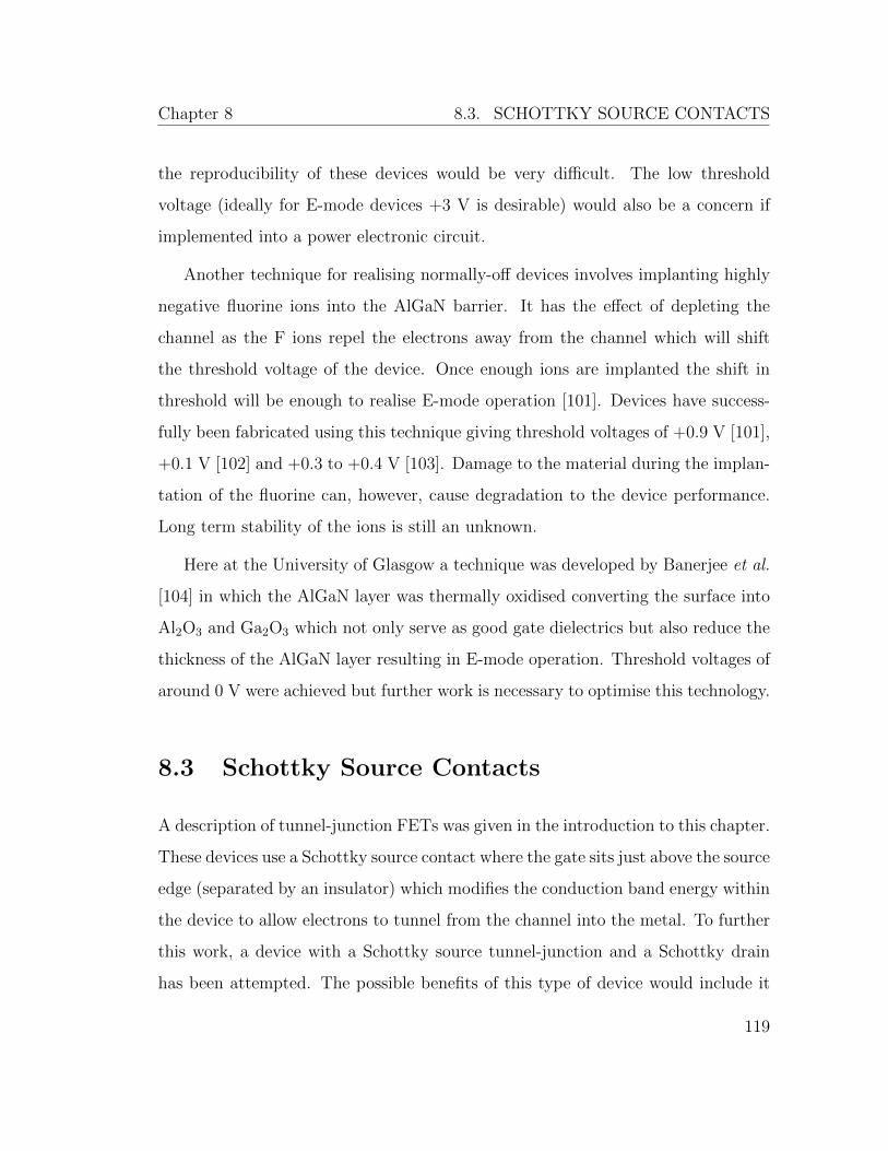
Chapter 8 8.3. SCHOTTKY SOURCE CONTACTS
the reproducibility of these devices would be very difficult. The low threshold
voltage (ideally for E-mode devices +3 V is desirable) would also be a concern if
implemented into a power electronic circuit.
Another technique for realising normally-off devices involves implanting highly
negative fluorine ions into the AlGaN barrier. It has the effect of depleting the
channel as the F ions repel the electrons away from the channel which will shift
the threshold voltage of the device. Once enough ions are implanted the shift in
threshold will be enough to realise E-mode operation [101]. Devices have success-
fully been fabricated using this technique giving threshold voltages of +0.9 V [101],
+0.1 V [102] and +0.3 to +0.4 V [103]. Damage to the material during the implan-
tation of the fluorine can, however, cause degradation to the device performance.
Long term stability of the ions is still an unknown.
Here at the University of Glasgow a technique was developed by Banerjee et al.
[104] in which the AlGaN layer was thermally oxidised converting the surface into
Al2O3 and Ga2O3 which not only serve as good gate dielectrics but also reduce the
thickness of the AlGaN layer resulting in E-mode operation. Threshold voltages of
around 0 V were achieved but further work is necessary to optimise this technology.
8.3 Schottky Source Contacts
A description of tunnel-junction FETs was given in the introduction to this chapter.
These devices use a Schottky source contact where the gate sits just above the source
edge (separated by an insulator) which modifies the conduction band energy within
the device to allow electrons to tunnel from the channel into the metal. To further
this work, a device with a Schottky source tunnel-junction and a Schottky drain
has been attempted. The possible benefits of this type of device would include it
119

Chapter 8 8.3. SCHOTTKY SOURCE CONTACTS
being a normally-off device (highly desired for power electronics) and the smooth,
drain contact which was described in chapter 6 leading to higher breakdown fields.
In order to assess the quality of the source contact, four different devices layouts
were considered. These were:
1. Ohmic source and Ohmic drain (known to work well for AlGaN/GaN HEMTs)
2. Ohmic source and Schottky drain (again known to work as described in section
6.3)
3. Schottky source with gate overlapping and Ohmic drain
4. Schottky source with gate overlapping and Schottky drain (shown in Fig. 8.1).
8.3.1 Fabrication
All the devices listed above were fabricated on the same sample to make fair com-
parisons. The material used was provided by Cambridge University and consisted
of a 2 nm GaN cap layer, a 20 nm AlGaN barrier with 23% Al content, a 1 nm AlN
exclusion layer, a 2 µm GaN buffer layer and a sapphire substrate. The provided
data accompanying the material give the sheet resistance to be 323 Ω/sq, carrier
concentration to be 9.7 x 1012cm−2 and electron mobility to be 1996 cm2/Vs.
Fabrication began with defining and forming all the Ohmic contacts in the
standard way, dry-etching of the AlGaN to the 2DEG for the Schottky contacts,
deposition of the Schottky Ti/Au layer in these recessed regions (10 nm/10 nm),
deposition of 10 nm of Si3N4 over the entire sample by plasma-enhanced chemical
vapour deposition (PECVD) at 300C to act as the gate insulator, and finally gate
and bond pad contacts. In [20] Al2O3 was used as the gate insulator but since this
120
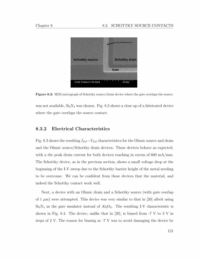
Chapter 8 8.3. SCHOTTKY SOURCE CONTACTS
Schottky source Schottky drain
Gate
Gate overlapping source
Figure 8.2: SEM micrograph of Schottky source/drain device where the gate overlaps the source.
was not available, Si3N4 was chosen. Fig. 8.2 shows a close up of a fabricated device
where the gate overlaps the source contact.
8.3.2 Electrical Characteristics
Fig. 8.3 shows the resulting IDS−VDS characteristics for the Ohmic source and drain
and the Ohmic source/Schottky drain devices. These devices behave as expected,
with a the peak drain current for both devices reaching in excess of 600 mA/mm.
The Schottky device, as in the previous section, shows a small voltage drop at the
beginning of the I-V sweep due to the Schottky barrier height of the metal needing
to be overcome. We can be confident from these devices that the material, and
indeed the Schottky contact work well.
Next, a device with an Ohmic drain and a Schottky source (with gate overlap
of 1 µm) were attempted. This device was very similar to that in [20] albeit using
Si3N4 as the gate insulator instead of Al2O3. The resulting I-V characteristic is
shown in Fig. 8.4. The device, unlike that in [20], is biased from -7 V to 3 V in
steps of 2 V. The reason for biasing at -7 V was to avoid damaging the device by
121

Chapter 8 8.3. SCHOTTKY SOURCE CONTACTS
0 2 4 6 8 100
100
200
300
400
500
600
700 Ohmic drain
Schottky drain
I DS (
mA
/mm
)
VDS
(V)
-1V
0V
-5V
-5V
-3V
VG - 7V to 0V
-7V
Figure 8.3: IDS−VDS characteristics for devices with Ohmic source and Ohmic/Schottky drain.
0 2 4 6 8 100.0
0.5
1.0
1.5
2.0
2.5
3.0
I DS (
mA
/mm
)
VDS
(V)
-3V
3V
1V
-1V
-5V
-7V
Figure 8.4: IDS − VDS characteristics for device with Schottky source and Ohmic drain.
122

Chapter 8 8.3. SCHOTTKY SOURCE CONTACTS
applying high forward biases to it initially (in case of high currents). Once confident,
the gate bias was steadily increased and the resulting drain current measured. It
can be seen from Fig. 8.4 that very little current flows in the device, which is what
is to be expected for an E-mode device at negative gate bias. However, once the
gate voltage reaches +3 V, it would be expected that a sufficient drain current
would be flowing, if the theory from [20] is correct. It can be seen though that
very little current is flowing, and indeed that the device is essentially switched
off. Further increase in the gate voltage resulted in very large gate currents and
indeed the device ceased to work. This indicates that the application of a forward
biased gate voltage is not controlling the conduction band energy as we would
desire it to. This result was not limited to one sample. Several fabrication runs
were carried out, varying parameters such as etch depth of the Schottky contact
recess, using room temperature inductively coupled plasma (ICP) Si3N4 instead of
PECVD, and the type of Schottky contact metal (i.e. Ni instead of Ti). All samples
showed similar characteristics to those given in this chapter. At this time we are
unable to explain the characteristic shown in Fig. 8.4. However, we contacted the
academic who first proposed the AlGaN/GaN tunnel junction concept indicating
our inability to replicate his published results. He responded by saying that they
themselves are unable to reproduce their own results and are not developing this
concept any further at the moment [105].
8.3.3 Simulated Conduction Band Profiles
To gain further insight as to why the Schottky source with gate overlapping device
was not working, some simulations (again similar to that given in [20]) focussing
on the conduction band energy were carried out. The simulations were carried out
in Sentaurus, as was described in chapter 4. Fig. 8.5 shows the resulting data from
123

Chapter 8 8.3. SCHOTTKY SOURCE CONTACTS
these simulations. The contact type for the source was set to Schottky and used a
work function of 4.33 eV (i.e. Ti) and the gate dielectric was Si3N4 (10 nm) where
εr = 7.1.
It is shown that at with a 0 V gate bias, the Schottky barrier width is approxi-
mately 18 nm wide, about 8 nm wider than is given in [20]. As the gate voltage is
increased we can see that the barrier width decreases (the Schottky barrier height
remains constant at about 0.9 eV). This is the pattern we expect but it can be
seen that even at +10 V bias on the gate contact, the Schottky barrier width only
decreases to about 6 nm which may still be too wide for electron tunnelling to be
effective. The insulator breaks down at around VG = 5 - 6 V as it is very thin and
so a further increase in gate voltage is not desirable.
8.3.4 Devices using SiO2
As a final fabrication run, it was felt that making some devices using SiO2 as the
gate dielectric may have some value. Again this choice was due to the availability
of SiO2 as a dielectric in the JWNC and that it has a wider band gap than Si3N4,
(∼ 9 eV compared to ∼ 5 eV) which is closer to the Al2O3 band gap (∼ 9 eV)
used in [20]. The fabrication for these devices was carried out in the same way as
described in section 8.3.1 except using SiO2 instead of Si3N4 as the gate insulator.
These devices, however, again did not display the functionality that we would have
liked i.e. switched on with the application of a positive gate bias. The results
are shown in Fig. 8.6 for completeness. This characteristic could be attributed to
electrons in the 2DEG and/or bulk leaking through the drain contact. As the gate
current increases the drain current decreases which would be an indication that the
gate leakage was increasing (therefore less available electrons for the drain). Since
124

Chapter 8 8.3. SCHOTTKY SOURCE CONTACTS
0.990 0.995 1.000 1.005 1.010 1.015 1.020
0.0
0.5
1.0
1.5
2.0C
on
du
cti
on
Ba
nd
En
erg
y (
eV
)
Cross section along 2DEG (um)
-5 V
0 V
3 V
5 V
10 V
Schottky
Metal
Increasing gate
voltage
2DEG
Schottky
Barrier Height
Figure 8.5: Simulated data from Sentaurus showing conduction band energy at the interfacebetween the source and the 2DEG as a function of gate voltage. 10 nm of Si3N4 is used in thissimulation as the gate dielectric. It can be observed that even at a gate voltage of 10 V theSchottky barrier width is probably still too wide for effective electron tunnelling.
the current is so low though it is reasonable to assume that the electrons are not
tunnelling effectively from the source to the 2DEG.
8.3.5 Discussion
A tunnel-junction FET on AlGaN/GaN HEMT material similar to that in [20]
has been attempted and been unsuccessful. I-V characteristics of a Schottky drain
device reveal that the Schottky contact is functional when forward biased but using
the gate to modify the conduction band energy of the reversed biased source contact
proved to be more challenging. The simulated data given in Fig. 8.5 reveals that
the Schottky barrier width may not be narrow enough (using Si3N4 as the gate
125

Chapter 8 8.3. SCHOTTKY SOURCE CONTACTS
0 2 4 6 8 100.00
0.01
0.02
0.03
0.04
0.05
0.06
I DS (
mA
/mm
)
VDS
(V)
0V
1V
2V
3V
4V
5V
Increasing gate voltage
Figure 8.6: IDS − VDS characteristics for device with Schottky source and Ohmic drain usingSiO2 as the gate dielectric.
dielectric) for electron tunnelling without applying a very high gate bias which is
counter-productive since this would cause breakdown of the insulating material.
Further devices were fabricated using SiO2 as the gate dielectric but these again
did not work as desired. These results are in contrast to those given by L. Yuan
et al. [20] who reported to have successfully implemented this design and showed
simulated characteristics which indicated that the barrier width was indeed narrow
enough for effective electron tunnelling.
126
Chapter 8 8.4. CONCLUSIONS
8.4 Conclusions
The work carried out in this chapter had the aim of implementing AlGaN/GaN
HEMTs with Schottky source and drain. The reasons for this is that an E-mode
device could potentially be made with the added benefits of a Schottky drain con-
tact. Although the Schottky drain contact showed promising results, i.e. high drain
current and breakdown fields in chapter 6, the tunnel-junction source contact failed
to work on several attempts using two different gate insulators. Simulated evidence
was given to back up the possible failure of this contact but the work is in contrast
to previous attempts by one other research group.
127

Chapter 9
Conclusions, Discussions and
Future Work
The overwhelming focus of this work was to create AlGaN/GaN HEMTs which
could gain the maximum potential out of the material through good design and
straight forward fabrication. The breakdown field of GaN is roughly 300 V/µm in
theory, but this number has never been reached with regards to lateral AlGaN/GaN
HEMTs. It is important to try and get closer to this theoretical value because
GaN based devices are likely to dominate high power electronics applications in
the near future and having highly efficient, cost effective devices is crucial. The
work was split into various aspects which were device simulation, fabrication and
characterisation. The device designs included MIS-HEMTs which incorporated a
Schottky drain contact, a new AlGaN/GaN device concept where the gate overlaps
the source and drain where the large electric field usually found at the drain edge
of the gate is eliminated and a device which had both Schottky source and drain
contacts. The simulations, designs and results are summarised in the following
128
Chapter 9 9.1. SIMULATED WORK
sections.
9.1 Simulated Work
The simulated work carried out in chapter 4 was intended to give an insight into
the large electric fields found in AlGaN/GaN devices under high biasing operation.
The electric field which is formed at the drain-edge of the gate was shown to be
effectively suppressed with the inclusion of a dielectric beneath the gate which
would imply a higher drain voltage is required to be achieve breakdown. Although
chapter 3 outlined several previous publications which used a dielectric beneath
the gate, there were no reports as to what the difference between as Schottky gate
device and a MIS-HEMT was. A more detailed model using one of the higher level
transport models i.e. hydrodynamic or Monte Carlo could also be used to assess
the how the suppressed electric field effects the impact ionisation which (as was
described in section 2.6.2) is attributed to causing the breakdown of the devices.
This would require very intimate knowledge of the simulator.
Further, a gate overlapping device where the gate overlapped the drain and
source contacts was shown to effectively eliminate this field altogether, however
this section of work did not include an analysis of the gate edge contact which sits
in close proximity to the drain contact.
Some issues with the simulated work which might deem it to be incomplete
is that the AlGaN/GaN model was not calibrated for a particular device and so
proper I-V characteristics could not be carried out. However, it was shown that
there existed a 2DEG and the conduction band profile for the material was what
would be expected. For these reasons, we can be confident that the electric field
analysis was a fair representation of a proper device.
129
Chapter 9 9.2. MIS-HEMTS
It should also be noted that devices were simulated without the inclusion of
a passivation layer (which would normally be included as a final step in real life
production). At high biasing the simulator would struggle to converge to a solution
and so the passivation layer was left out to limit the amount of calculations required
to be carried out allowing for faster feedback.
9.2 MIS-HEMTs
9.2.1 Overview
Chapter 6 gave results for breakdown characteristics for Schottky gate HEMTs and
MIS-HEMTs. This section of work was carried out on the basis of the simulated
results given in chapter 4 which showed how an insulator beneath the gate sup-
pressed the electric field at the drain-edge of the gate. The experimental results
clarified the simulated data and improvements in breakdown voltages between the
Schottky gate and MIS-HEMT devices were given (coupled with reduced gate leak-
age currents). The MIS-HEMTs showed further improvements in the breakdown
voltage with the inclusion of Schottky drain contact and a high breakdown field of
86.6 Vµm was measured for a device with a gate-to-drain distance of 2.5 µm. Issues
of inconsistency in the dielectric used (PECVD Si3N4) were also reported in terms
of threshold voltage, gate leakage and transconductance but it was felt that these
did not have an impact on the breakdown voltage and may have been attributed
to the deposition quality.
From the breakdown results, however, it can be said that a MIS-HEMT in-
corporating a Schottky drain contact gives the largest breakdown voltage. These
techniques have shown to gain much more potential out of the material and should
130

Chapter 9 9.2. MIS-HEMTS
be considered when designing devices for high power applications in the future.
9.2.2 Future Work
From the beginning of this section of work, it was felt that an ultimate solution
for these devices would incorporate an atomically layer deposited (ALD) dielectric
such as HfO2 or Al2O3. Not only have these dielectrics shown to improve device
performance in the past [58, 98], they are deposited in such a way that they are
uniform across an entire wafer. This would not only lead to very high power devices
but also high yield and consistency.
The work carried out in this chapter could also be coupled with the work carried
out on the buffer layer thickness work carried out in [49]. In their conclusions they
state that their breakdown is now limited by the peak electric field at the drain-edge
of the gate and so by combining this work and their work, very high breakdown
fields may be achieved.
Recent work carried out in the JWNC (within the research group) has shown
that inductively coupled plasma deposited Si3N4 gives more consistent results across
a sample as well as showing comparable device characteristics such as drain and gate
leakage current. A breakdown analysis using this dielectric has not been carried
out and it would be interesting to see how it compared with the PECVD Si3N4.
131

Chapter 9 9.3. GATE OVERLAPPING HEMT
9.3 Gate Overlapping HEMT
9.3.1 Overview
The gate overlapping HEMT was first introduced in chapter 4 where simulated
results were given. The design aimed to eliminate the large electric field usually
found at the drain edge of the gate by overlapping the drain with the gate. The
simulated results did indeed show that the peak electric field found at the drain-
side of the gate was completely eliminated. In chapter 7 experimental results were
provided for this designs. Variations in processing were required (e.g. reduction
in Ohmic contact height, increase of dielectric thickness) in order to fabricate a
working device. The overlapping structures showed very low breakdown voltages
(6 - 10 V) which was attributed to the closeness of the gate contact and the drain
contact, separated by only a thin layer of dielectric.
9.3.2 Future Work
Gate overlapping HEMTs are still at a very early stage and clearly issues between
the gate and drain contact must be addressed. Thicker dielectrics with higher di-
electric constants may help to improve the breakdown voltages of this type of device
structure but it is very unlikely that the high breakdown potential of AlGaN/GaN
would be realised using this device concept. Fabrication of this device still contin-
ues within the research group with the aim of realising E-mode devices (shown in
the next section) for high current, low voltage application.
132

Chapter 9 9.3. GATE OVERLAPPING HEMT
Source
Schottky
Drain
GaN
3 nm AlGaN
Dielectric
Gate
No natural 2DEG
LG
Substrate
Figure 9.1: Material and device structure for E-mode operation with high breakdown voltages.
9.3.3 Enhancement Mode Devices
The overlapping device structure also lends itself to realising E-mode devices where
a thin AlGaN barrier is used (3 nm). The structure for this type of device is shown
in Fig. 9.1. Since the AlGaN layer is below the critical thickness at which the
2DEG forms, the material is naturally non-conductive and devices fabricated on it
will be normally-off. If, however, a gate overlapping structure is used (similar to
this work) and a positive bias is placed on the gate, the conduction band energy will
be lowered and free electrons which will come from the Ohmic contact areas will
create a 2DEG and a current will flow under drain-source bias. Some preliminary
results within the research group have shown this structure to give an encouraging
VTH of + 3 V.
133

Chapter 9 9.4. SCHOTTKY SOURCE AND DRAIN HEMT
9.4 Schottky source and drain HEMT
9.4.1 Overview
The ultimate aim of this section of work was to create an E-mode device (similar
to that in [20]) whilst also giving superior breakdown performance to compared to
devices which used an Ohmic drain. The Schottky drain contact was shown to be
effective in increasing the breakdown voltage, from 122 V to 166 V in chapter 6 for
similar sized devices but, even after several attempts and processing adjustments,
the Schottky source tunnel junction was unsuccessful. Simulated conduction band
diagrams were given which outlined why it may not be working which, in contrast
to [20], showed that Schottky barrier width with a gate voltage of 10 V, was still
not adequate to allow electron tunnelling.
9.4.2 Future Work
A cumulative time of almost six months was dedicated to this work, through de-
vice process and simulation. At no time did the Schottky source contact look
as if it was working in the way in which we initially expected. The structure is
essentially two Schottky diodes back-to-back and should not work under normal
circumstances. The theory given in [20] suggested that with the gate sitting just
above the source contact, tunnelling of electrons could occurs once the Schottky
barrier width reached 1 nm but this was not the case. For the amount of time
invested in this work it was hoped that it would be rewarded with a normally-off
device which exhibited very high breakdown fields.
For future power devices developed here in Glasgow, a Schottky drain contact
should be used. A better understanding of this type of tunnel junction is required
134

Chapter 9 9.5. GENERAL COMMENTS AND OBSERVATIONS
for this work to progress.
9.5 General comments and observations
Gallium nitride based technology will surely be the dominant force in high power
and high frequency electronics in the years to come. Full engineering solutions
to gain the maximum potential from this material have not yet been realised and
the work in this thesis has attempted to further the knowledge of what makes a
difference in trying to realise the full potential. One aspect which has not been
considered here is thermal issues associated with these devices. The devices in
this work were all fabricated using sapphire as the substrate (which has a thermal
conductivity of 0.3 W/cm K) but for commercial high powered devices SiC is used
as the substrate (which has a thermal conductivity of 4.9 W/cm K). However, even
these devices will not make full use of their highly thermally conductive substrate
because the channel, and therefore the heat, is generated almost 2 µm away from it
(GaN only has a thermal conductivity of 1.3 W/cm K). Solutions must be found to
make sure the heat generated in these devices is removed as efficiently as possible
from the channel and therefore GaN based technology will be one step closer to
realising its full potential.
GaN-on-Si is another large aspect which has not been considered. From an
economic point of view, GaN-on-Si is by far the way forward with regards to high
power electronics. A great deal of research and development is currently being
invested in this area around the world and will contribute to automotive, aerospace,
consumer electronics, lighting, healthcare and energy industries.
Fabrication technologies such as atomic layer deposition, dry-etch processes and
exotic materials used for Ohmic and gate contacts are also making the engineering
135

Appendix A
of these types of devices reach new limits. However, engineering on its own will not
be the only way in which the full exploitation of this material is furthered and new
material structures, such as that mentioned in 9.3.3 will also have to be considered.
136

Appendix A
Appendix A
Fabrication of AlGaN/GaN HEMTs using photolithography
Both Schottky gate and MIS-HEMTs follow similar processes with the exception of
the gate dielectric deposition and etch. Schottky drain contact formation shall also
be included in the description, however, it is not always a necessary step.
Device cleaning
1. Place sample in glass beaker of acetone and put into ultrasonic bath for 15
minutes
2. Rinse with IPA
3. Blow dry with N2
Mesa isolation
1. Spin S1818 photoresist onto sample at 4000 rpm, with an acceleration of 1000
rpm for 2 minutes
2. Bake on hotplate for 2 minutes at 65C
3. Expose to UV light using MA6 for 5 seconds in vacuum contact
4. Post exposure development in (1:1) Microposit Developer Concentrate : RO
water for 1 minute 15 seconds
137

Appendix A
5. Rinse thoroughly in RO water
6. Blow dry with N2
7. O2 ash for 3 minutes at 60 W
8. Hard bake on hotplate at 90C for 3 minutes
9. Etch in ICP-180 using Cl2/BCl3/Ar with gas flows of 20/5/10 sccm, pressure
of 10 mT, RF power of 28 W and ICP power of 100 W for 5 minutes.
10. Soak in acetone at 50C
11. Rinse with IPA
Ohmic contact formation
1. Spin S1818 photoresist onto sample at 4000 rpm, with an acceleration of 1000
rpm for 2 minutes
2. Bake on hotplate for 2 minutes at 65C
3. Post bake develop sample in (1:1) Microposit Developer Concentrate : RO
water for 1 minute. No agitation.
4. Rinse thoroughly with water
5. Blow dry with N2
6. Expose to UV light using MA6 for 5 seconds in vacuum contact
7. Post exposure development in (1:1) Microposit Developer Concentrate : RO
water for 1 minute 15 seconds. Agitate if necessary.
138

Appendix A
8. Rinse thoroughly in RO water
9. Blow dry with N2
10. O2 ash for 3 minutes at 60 W
11. De-oxidise in 4H2O:HCl for 30 seconds
12. Deposit Ti/Al/Ni/Au - 30/180/40/100 nm using electron beam evaporator
13. Lift-off metal using acetone at 50C for 10 - 15 minutes
14. Rinse in IPA
15. Blow dry with N2
16. Anneal metal at 800C for 30 seconds in N2
Schottky drain contact formation
1. Spin S1818 photoresist onto sample at 4000 rpm, with an acceleration of 1000
rpm for 2 minutes
2. Bake on hotplate for 2 minutes at 65C
3. Post bake develop sample in (1:1) Microposit Developer Concentrate : RO
water for 1 minute. No agitation.
4. Rinse thoroughly with water
5. Blow dry with N2
6. Expose to UV light using MA6 for 5 seconds in vacuum contact
139

Appendix A
7. Post exposure development in (1:1) Microposit Developer Concentrate : RO
water for 1 minute 15 seconds. Agitate if necessary.
8. Rinse thoroughly in RO water
9. Blow dry with N2
10. O2 ash for 3 minutes at 60 W
11. Hard bake on hotplate at 90C for 3 minutes
12. Etch in ICP-180 using Cl2/BCl3 with gas flows of 10/5 sccm, pressure of 20
mT, RF power of 13 W and ICP power of 100 W for 3 minutes.
13. Deposit Ni/Pt - 5/50 nm
14. Lift-off metal using acetone at 50C for 10 - 15 minutes
15. Rinse with IPA
16. Blow dry with N2
Gate contact formation
1. Spin S1805 photoresist onto sample at 4000 rpm, with an acceleration of 1000
rpm for 2 minutes
2. Bake on hotplate for 2 minutes at 65C
3. Post bake develop sample in (1:1) Microposit Developer Concentrate : RO
water for 1 minute. No agitation.
4. Rinse thoroughly with water
140

Appendix A
5. Blow dry with N2
6. Expose to UV light using MA6 for 3 seconds in vacuum contact
7. Post exposure development in (1:1) Microposit Developer Concentrate : RO
water for 1 minute 15 seconds. Agitate if necessary.
8. Rinse thoroughly in RO water
9. Blow dry with N2
10. O2 ash for 1 minute at 60 W
11. Deposit Ni/Au - 20/200 nm using electron beam evaporator
12. Lift-off metal using acetone at 50C for 10 - 15 minutes
13. Rinse in IPA
14. Blow dry with N2
Bond pads
1. Spin S1818 photoresist onto sample at 4000 rpm, with an acceleration of 1000
rpm for 2 minutes
2. Bake on hotplate for 2 minutes at 65C
3. Post bake develop sample in (1:1) Microposit Developer Concentrate : RO
water for 1 minute. No agitation.
4. Rinse thoroughly with water
141

5. Blow dry with N2
6. Expose to UV light using MA6 for 5 seconds in vacuum contact
7. Post exposure development in (1:1) Microposit Developer Concentrate : RO
water for 1 minute 15 seconds. Agitate if necessary.
8. Rinse thoroughly in RO water
9. Blow dry with N2
10. O2 ash for 3 minute at 60 W
11. Deposit Ti/Au - 20/200 nm using electron beam evaporator
12. Lift-off metal using acetone at 50C for 10 - 15 minutes
13. Rinse in IPA
14. Blow dry with N2
Gate dielectric for MIS-HEMTs
1. After Ohmic contact formation (and Schottky drain if utilising), blanket de-
posit 10 nm of Si3N4 across sample using PECVD
2. Si3N4 must be etched to make electrical contact with source, drain and gate.
This is done after the gate contact formation using the BP80+ etch tool, with
CHF3/O2 with gas flows of 50/5 sccm, pressure of 55 mT, RF power of 150
W for 17 seconds.
142

References
[1] M. A. Khan, A. Bhattarai, J. N. Kuznia, and D. T. Olson, “High electron
mobility transistor based on a GaN-AlGaN heterojunction,” Applied Physics
Letters, vol. 63, pp. 1214 – 1215, 1993.
[2] M. A. Khan, J. N. Kuznia, D. T. Olson, W. J. Schaff, J. W. Burm, and M. S.
Shur, “Microwave performance of a 0.25µm gate AlGaN/GaN heterostructure
field effect transistor,” Applied Physics Letters, vol. 65, no. 9, pp. 1121 –1123,
1994.
[3] Semiconductor Today, “GaN power electronics market may top $ 1bn
in a few years,” accessed March 2013. http://www.semiconductor-
today.com/news items/2012/MAR/YOLE 080312.html.
[4] H. Okumura, “Present status and future prospect of widegap semicondcutor
high power devices,” Japanese Journal of Applied Physics, vol. 45, no. 10A,
pp. 7565 – 7586, 2006.
[5] R. J. Trew, “SiC and GaN transistors - Is there one winner for microwave
power applications?,” Proceedings of the IEEE, vol. 90, pp. 1032 – 1047, June
2002.
[6] R. Kemerley, H. Wallace, and M. Yoder, “Impact of wide bandgap microwave
143

devices on DoD systems,” Proceedings of the IEEE, vol. 90, no. 6, pp. 1059–
1064, June.
[7] A. Fontsere, A. Perez-Tomas, V. Banu, P. Godignon, J. Millan,
H. De Vleeschouwer, J. M. Parsey, and P. Moens, “A HfO2 based 800V/300c
Au-free AlGaN/GaN-on-Si HEMT technology,” in 2012 24th International
Symposium on Power Semiconductor Devices and ICs (ISPSD), pp. 37–40,
2012.
[8] I. Daumiller, C. Kirchner, M. Kamp, K. Ebeling, and E. Kohn, “Evaluation
of the temperature stability of AlGaN/GaN heterostructure FETs,” IEEE
Electron Device Letters, vol. 20, no. 9, pp. 448–450, 1999.
[9] E. Johnson, “Physical limitations on frequency and power parameters of tran-
sistors,” in IRE International Convention Record, vol. 13, pp. 27 – 34, March
1965.
[10] B. J. Baliga, “Semiconductors for high-voltage, vertical channel field-effect
transistors,” Journal of Applied Physics, vol. 53, pp. 1759 – 1764, 1982.
[11] B. J. Baliga, “Power semiconductor device figure of merit for high-frequency
applications,” IEEE Electron Device Letters, vol. 10, no. 10, pp. 455–457,
1989.
[12] R. W. Keyes, “Figure of merit for semiconductors for high speed switches,”
IEEE Proceedings, vol. 10, p. 225, 1972.
[13] O. Ambacher, J. Smart, J. R. Shealy, N. G. Weimann, K. Chu, M. Mur-
phy, W. J. Schaff1, L. F. Eastman, R. Dimitrov, L. Wittmer, M. Stutz-
mann, W. Rieger, and J. Hilsenbeck, “Two-dimensional electron gases in-
144

duced by spontaneous and piezoelectric polarization charges in N- and Ga-
face AlGaN/GaN heterostructures,” Journal of Applied Physics, vol. 85, no. 6,
pp. 3222 – 3233, 1999.
[14] J. Kuzmik, “Power electronics on InAlN/(In)GaN: Prospect for a record per-
formance,” IEEE Electron Device Letters, vol. 22, pp. 510 –512, November
2001.
[15] Y. Cao and D. Jena, “High-mobility window for two-dimensional elec-
tron gases at ultrathin AlN/GaN heterojunctions,” Applied Physics Letters,
vol. 90, no. 18, p. 182112, 2007.
[16] S. Taking, D. Macfarlane, and E. Wasige, “AlN/GaN MOS-HEMTs with ther-
mally grown passivation,” IEEE Transactions on Electron Devices, vol. 58,
pp. 1418 –1424, May 2011.
[17] E. J. Miller, X. Z. Dang, and E. T. Yu, “Gate leakage current mechanisms
in AlGaN/GaN heterostructure field effect transistors,” Journal of Applied
Physics, vol. 88, pp. 5951 – 5958, November 2000.
[18] E. T. Yu, X. Z. Dang, L. S. Yu, D. Qiao, P. M. Asbeck, S. S. Lau, G. J.
Sullivan, K. S. Boutros, and J. M. Redwing, “Schottky barrier engineering in
III - V nitrides via the piezoelectric effect,” Applied Physics Letters, vol. 73,
no. 13, p. 1880, 1998.
[19] U. K. Mishra, “AlGaN/GaN transistors for power electronics,” in 2010 IEEE
International Electron Devices Meeting (IEDM), pp. 13.2.1 –13.2.4, December
2010.
[20] L. Yuan, H. Chen, and K. J. Chen, “Normally off AlGaN/GaN 2DEG
145

tunnel-junction field-effect transistors,” IEEE Electron Device Letters, vol. 32,
pp. 303–305, March 2011.
[21] F. Bernardini, V. Fiorentini, and D. Vanderbilt, “Spontaneous polarization
and piezoelectric constants of III-V nitrides,” Physical Review B, vol. 56,
pp. R10024–R10027, Oct 1997.
[22] S. Rajan, A. Chini, M. H. Wong, J. S. Speck, and U. K. Mishra, “N-polar
GaN/AlGaN/GaN high electron mobility transistors,” Journal of Applied
Physics, vol. 102, no. 4, p. 044501, 2007.
[23] J. H. Edgar, S. Strite, I. Akasaki, H. Amano, and C. Wetzel, Gallium Nitride
and Related Semiconductors. INSPEC, 1999.
[24] O. Ambacher, B. Foutz, J. Smart, J. R. Shealy, N. G. Weimann, K. Chu,
M. Murphy, A. J. Sierakowski, W. J. Schaff, and L. F. Eastman, “Two-
dimensional electron gases induced by spontaneous and piezoelectric polar-
ization charges undoped and doped AlGaN/GaN hetereostructures,” Journal
of Applied Physics, vol. 87, no. 1, pp. 334 – 344, 2000.
[25] R. Quay, Gallium Nitride Electronics. Springer, 2008.
[26] G. I. Ng, S. Arulkumaran, S. Vicknesh, H. Wang, K. S. Ang, C. M. M. Kumar,
K. Ranjan, G.-Q. Lo, S. Tripathy, C. C. Boon, and W. M. Lim, “GaN-on-
Silicon integration technology,” in 2012 IEEE International Symposium on
Radio-Frequency Integration Technology (RFIT), pp. 159–161, November.
[27] J. P. Ibbetson, P. T. Fini, K. D. Ness, S. P. DenBaars, J. S. Speck, and U. K.
Mishra, “Polarisation effects, surface states, and the source of electrons in
AlGaN/GaN heterostructure field effect transistors,” Applied Physics Letters,
vol. 77, July 2000.
146

[28] I. P. Smorchkoba, C. R. Elsass, J. P. Ibbetson, R. Vetury, B. Heying, P. Fini,
E. Haus, S. P. DenBaars, J. S. Speck, and U. K. Mishra, “Polarization-
induced charge and electron mobility in AlGaN/GaN heterostructures grown
by plasma assisted molecular beam epitaxy,” Journal of Applied Physics,
vol. 86, pp. 4520 – 4526, October 1999.
[29] S. Taking, AlN/GaN MOS-HEMTs Technology. PhD thesis, School of Engi-
neering, University of Glasgow, 2012.
[30] B. V. Daele, G. V. Tendeloo, a. J. D. W. Ruythooren, M. R. Leysand, and
M. Germain, “The role of Al on Ohmic contact formation on n-type GaN and
AlGaN/GaN,” Applied Physics Letters, vol. 87, pp. 061905 – 061908, 2005.
[31] B. Jacobs, M. Kramer, E. Geluk, and F. Karouta, “Optimisation of the
Ti/Al/Ni/Au Ohmic contact on AlGaN/GaN FET structures,” Journal of
Crystal Growth, vol. 241, pp. 15 – 18, 2002.
[32] R. Gong, J. Wang, S. Liu, Z. Dong, M. Yu, C. P. Wen, Y. Caia, and B. Zhang,
“Analysis of surface roughness in Ti/Al/Ni/Au ohmic contact to AlGaN/GaN
high electron mobility transistors,” Applied Physics Letters, vol. 97, no. 6,
p. 062115, 2010.
[33] A. Basu, F. M. Mohammed, S. Guo, B. Peres, and I. Adesida,
“Mo/Al/Mo/Au Ohmic contact scheme for AlGaN/GaN high electron mobil-
ity transistors annealed at 500,” Journal of Vacuum Science and Technology
B, pp. L16 – L18, March/April 2006.
[34] B. Lu, E. L. Piner, and T. Palacios, “Schottky-drain technology for Al-
GaN/GaN high-electron mobility transistors,” IEEE Electron Device Letters,
vol. 31, pp. 302 –304, April 2010.
147

[35] E. Bahat-Treidel, R. Lossy, J. Wurfl, and G. Trankle, “AlGaN/GaN HEMT
with integrated recessed schottky-drain protection diode,” IEEE Electron De-
vice Letters, vol. 30, pp. 901 –903, September 2009.
[36] R. Pierret, Semiconductor Device Fundamentals. Addison Wesley, 1996.
[37] M. G. et al., “High electron mobility in AlGaN/GaN HEMT grown on sap-
phire: strain modification by means of AlN interlayers,” Proceedings of MRS
Fall 2003 Conference, December 2003.
[38] B. G. Street and S. Banerjee, Solid State Electronic Devices. Prentice Hall,
2005.
[39] R. Vetury, N. Q. Zhang, S. Keller, and U. K. Mishra, “The impact of surface
states on the DC and RF characteristics of AlGaN/GaN HFETs,” IEEE
Transactions on Electron Devices, vol. 48, pp. 560 –566, March 2001.
[40] L. F. Eastman, “Results, potential and challenges of high power GaN-based
transistors,” Solid State Physics, vol. 176, pp. 175 – 178, 1999.
[41] J. M. Tirado, J. L. Sanchez-Rojas, and J. I. Izpura, “Simulation of surface
state effects in the transient response of AlGaN/GaN HEMT and GaN MES-
FET devices,” Semiconductor Science and Technology, vol. 21, pp. 1150 –
1159, 2006.
[42] C. Kirkpatrick, B. Lee, R. Suri, X. Yang, and V. Misra, “Atomic layer depo-
sition of SiO2 for AlGaN/GaN MOS-HFETs,” IEEE Electron Device Letters,
vol. 33, pp. 1240 –1242, September 2012.
[43] M. Kuroda, T. Murata, S. Nakazawa, T. Takizawa, M. Nishijima, M. Yanag-
ihara, T. Ueda, and T. Tanaka, “High fmax with high breakdown voltage
148

in AlGaN/GaN MIS-HFETs using in-situ SiN as gate insulators,” in IEEE
Compound Semiconductor Integrated Circuits Symposium, pp. 1–4, October
2008.
[44] E. J. Miller and E. T. Y. X. Z Dang and, “Gate current leakage current
mechanisms in AlGaN/GaN heterostructure field-effect transistors,” Journal
of Applied Physics, vol. 88, pp. 5951 – 5957, November 2000.
[45] H. Kim, J. Lee, D. Liu, and W. Lu, “Gate current leakage and breakdown
mechanism in unpassivated AlGaN/GaN high electron mobility transistors
by post-gate annealing,” Applied Physics Letters, vol. 86, p. 143505, 2005.
[46] W. S. Tan, P. A. Houston, P. J. Parbrook, D. A. Wood, G. Hill, and C. R.
Whitehouse, “Gate leakage effects and breakdown voltage in metalorganic va-
por phase epitaxy AlGaN/GaN heterostructure field-effect transistors,” Ap-
plied Physics Letters, vol. 84, no. 17, pp. 3207 – 3209, 2002.
[47] M. H. Somerville and J. A. del Alamo, “A model for tunneling-limited break-
down in high-power HEMTs,” in International Electron Devices Meeting,
1996, pp. 35 –38, Dec. 1996.
[48] M. Faqir, G. Verzellesi, G. Meneghesso, E. Zanoni, and F. Fantini, “Investiga-
tion of high-electric-field degradation effects in AlGaN/GaN HEMTs,” IEEE
Transactions on Electron Devices, vol. 55, pp. 1592 –1602, July 2008.
[49] S. Selvaraj, T. Suzue, and T. Egawa, “Breakdown enhancement of Al-
GaN/GaN HEMTs on 4-in silicon by improving the GaN quality on thick
buffer layers,” IEEE Electron Device Letters, vol. 30, no. 6, pp. 587–589,
2009.
149

[50] M. Faqir, G. Verzellesi, A. Chini, F. Fantini, F. Danesin, G. Meneghesso,
E. Zanoni, and C. Dua, “Mechanisms of RF current collapse in AlGaN-GaN
high electron mobility transistors,” IEEE Transactions on Device and Mate-
rials Reliability, vol. 8, no. 2, pp. 240–247, 2008.
[51] J. Joh, L. Xia, and J. del Alamo, “Gate current degradation mechanisms of
GaN high electron mobility transistors,” in IEEE 2007 International Electron
Devices Meeting, pp. 385–388, 2007.
[52] T. Nakao, Y. Ohno, S. Kishimoto, K. Maezawa, and T. Mizutani, “Study
of off-state breakdown in AlGaN/GaN HEMTs,” Physics of the Solid State,
no. 7, pp. 2335 – 2338, 2003.
[53] M. Wang and K. J. Chen, “Off-state breakdown characterization in Al-
GaN/GaN HEMT using drain injection technique,” IEEE Transactions on
Electron Devices, vol. 57, pp. 1492–1496, July 2010.
[54] Y. Ohno, T. Nakao, S. Kishimoto, K. Maezawa, and T. Mizutani, “Effects
of surface passivation on breakdown of AlGaN/GaN high-electron-mobility
transistors,” Applied Physics Letters, vol. 84, no. 12, pp. 2184 – 2186, 2005.
[55] X. Z. Dang, R. J. Welty, D. Qiao, P. M. Asbeck, S. S. Lau, E. T. Yu, K. S.
Boutros, and J. M. Redwing, “Fabrication and characterisation of enhanced
barrier AlGaN/GaN HFET,” IEEE Electronics Letters, April 1999.
[56] N.-Q. Zhang, B. Moran, S. P. DenBaars, U. K. Mishra, X.-W. Wang, and T.-
P. Ma, “Effects of surface traps on breakdown voltage and switching speed of
GaN power switching HEMTs,” in 2001 IEDM Technical Digest International
Electron Devices Meeting, pp. 25.5.1–25.5.4, 2001.
150

[57] S. Chowdhury, M. H. Wong, B. L. Swenson, and U. K. Mishra, “CAVET on
bulk GaN substrates achieved with MBE-regrown AlGaN/GaN layers to sup-
press dispersion,” IEEE Electron Device Letters, vol. 33, pp. 41 –43, January
2012.
[58] J. Shi, L. F. Eastman, X. Xin, and M. Pophristic, “High performance Al-
GaN/GaN power switch with HfO2 insulation,” Applied Physics Letters,
vol. 95, no. 042103, 2009.
[59] T.-Y. Wu, S.-K. Lin, P.-W. Wen, J.-J. Huang, W.-C. Chien, C.-C. Hu,
M.-J. Tsai, and Y.-H. Wang, “AlGaN/GaN MOSHEMTs with liquid-phase-
deposited TiO2 as gate dielectric,” IEEE Transactions on Electron Devices,
vol. 56, no. 12, pp. 2911 – 2916, 2009.
[60] O. Seok, W. Ahn, Y.-S. Kim, M.-K. Han, and M.-W. Ha, “3.2 kV Al-
GaN/GaN MIS-HEMTs Employing RF sputtered Ga2O3 films,” in 24th In-
ternational Symposium on Power Semiconductor Devices and ICs (ISPSD),
pp. 269 – 272, June 2012.
[61] S. Yagi, M. Shimzu, H. Okumura, H. Ohashi, K. Arai, Y. Yano, and
N. Akutsu, “1.8 kV AlGaN/GaN HEMTs with high-k/Oxide/SiN MIS struc-
ture,” in Proceeding of 18th International Symposium on Power Semiconduc-
tor Devices and ICs, May 2007.
[62] W. S. Tan, P. A. Houston, G. Hill, R. J. Airey, and P. J. Parbook, “Electrical
characteristics of AlGaN/GaN metal-insulator semiconductor heterostructure
field-effect transistors and sapphire substrates,” Journal of Electronic Mate-
rials, vol. 32, no. 5, pp. 350 – 354, 2003.
151

[63] H.-S. Lee, D. S. Lee, and T. Palacios, “AlGaN/GaN high-electron-mobility
transistors fabricated through a Au-free technology,” IEEE Electron Device
Letters, vol. 32, no. 5, pp. 623–625, 2011.
[64] K. B. Lee, R. T. Green, P. A. Houston, W. S. Tan, M. J. Uren, D. J. Wal-
lis, and T. Martin, “Bi-layer SixNy passivation on AlGaN/GaN HEMTs to
suppress current collapse and improve breakdown,” Semiconductor Science
Technology, vol. 25, p. 125010, 2010.
[65] C. L. Chen, “Breakdown of overlapping-gate GaAs MESFETs,” IEEE Trans-
actions on Electron Devices, vol. 43, pp. 535 –542, April 1996.
[66] N. Q. Zhang, S. Keller, G. Parish, S. Heikman, S. P. DenBaars, and U. K.
Mishra, “High breakdown GaN HEMT with overlapping gate structure,”
IEEE Electron Device Letters, vol. 21, pp. 421 –423, September 2000.
[67] S. Karmalkar and U. K. Mishra, “Enhancement of breakdown voltage in
AlGaN/GaN high electron mobility transistors using a field plate,” IEEE
Transactions on Electron Devices, vol. 48, pp. 1515–1521, August 2001.
[68] Y. Okamoto, Y. Ando, T. Nakayama, K. Hataya, H. Miyamoto, T. Inoue,
M. Senda, K. Hirata, M. Kosaki, N. Shibata, and M. Kuzuhara, “High-
power recessed-gate AlGaN/GaN HFET with a field-modulating plate,” IEEE
Transactions on Electron Devices, vol. 51, pp. 2217 – 2222, December 2004.
[69] W. Saito, Y. Takada, M. Kuraguchi, K. Tsuda, I. Omura, T. Ogura, and
H. Ohashi, “High breakdown voltage AlGaN/GaN power-HEMT design and
high current density switching behavior,” IEEE Transactions on Electron
Devices, vol. 50, pp. 2528 – 2531, December 2003.
152

[70] B.-R. Park, J.-G. Lee, H.-J. Lee, J. Lim, K.-S. Seo, and H.-Y. Cha, “Break-
down voltage enhancement in field plated AlGaN/GaN-on-Si HFETs using
mesa-first prepassivation process,” IEEE Electronics Letters, vol. 48, pp. 181
–182, February 2012.
[71] Y. Dora, A. Chakraborty, L. McCarthy, S. Keller, S. P. DenBaars, and U. K.
Mishra, “High breakdown voltage achieved on AlGaN/GaN HEMTs with
integrated slant field plates,” IEEE Electron Device Letters, vol. 27, pp. 713
–715, September 2006.
[72] N. Zhang, V. Mehrotra, S. Chandrasekaran, B. Moran, L. Shen, U. Mishra,
E. Etzkorn, and D. Clarke, “Large area GaN power devices for power elec-
tronic applications: Switching and temperature characteristics,” in IEEE 34th
Annual Power Electronics Specialist Conference, vol. 1, pp. 233 – 237, June
2003.
[73] Y. S. Lin, J. Y. Wu, C. Y. Chan, S. S. H. Hsu, C. F. Huang, and T. C.
Lee, “Square-gate AlGaN/GaN HEMTs with improved trap-related charac-
teristics,” IEEE Transactions on Electron Devices, vol. 56, pp. 3207 – 3211,
December 2009.
[74] Synopsis Software [Online], May 2012. http://www.synopsys.com.
[75] K. Ota, K. Endo, Y. Okamoto, Y. Ando, H. Miyamoto, and H. Shimawaki, “A
normally-off GaN FET with high threshold voltage uniformity using a novel
piezo neutralization technique,” 2009 IEEE International Electron Devices
Meeting, pp. 1–4, 2009.
[76] Synopsis Documentation, Simulation of normally off GaN MISFET with
piezo neutralization technique.
153

[77] Synopsis, Sentaurus Workbench Comprehensive Frame-
work Environment [Online], Accessed March 2013.
http://www.synopsys.com/Tools/TCAD/CapsuleModule/swb ds.pdf.
[78] Synopsis, Sentaurus Structure Editor Device Editor
and Process Emulator [Online], Accessed March 2013.
http://www.synopsys.com/tools/tcad/capsulemodule/sde ds.pdf.
[79] Synopsis, Sentaurus Device User Guide.
[80] D. Qiao, Z. F. Guan, J. Carlton, S. S. Lau, and G. J. Sullivan, “Low re-
sistance ohmic contacts on AlGaN/GaN structures using implantation and
the advancing Al/Ti metallization,” Applied Physics Letters, vol. 74, no. 18,
p. 2652, 1999.
[81] I. P. Smorchkova, C. R. Elsass, J. P. Ibbetson, R. Vetury, B. Heying, P. Fini,
E. Haus, S. P. DenBaars, J. S. Speck, and U. K. Mishra, “Polarization-
induced charge and electron mobility in AlGaN/GaN heterostructures grown
by plasma-assisted molecular-beam epitaxy,” Journal of Applied Physics,
vol. 86, pp. 4520 – 4526, October 1999.
[82] Z. H. Liu, G. I. Ng, S. Arulkumaran, Y. K. T. Maung, K. L. Teo,
S. C. Foo, and V. Sahmuganathan, “Comprehensive study on the bias-
dependent equivalent-circuit elements affected by PECVD SiN passivation
in AlGaN/GaN HEMTs,” IEEE Transactions on Electron Devices, vol. 58,
pp. 473 –479, February 2011.
[83] Tanner EDA [Online], Accessed February 2013.
http://www.tannereda.com/products/l-edit-pro.
154

[84] Agilent [Online], Accessed February 2013.
http://www.home.agilent.com/en/pd-582565-pn-B1500A/semiconductor-
device-analyzer.
[85] A. Endoh, I. Watanabe, Y. Yamashita, T. Mimura, and T. Matsui, “Al-
GaN/GaN MIS-HEMTs with fT of 194 GHz at 16 K,” IEEE Electronics
Letters, vol. 44, no. 4, pp. 319 –320, 2008.
[86] J. Chung, W. Hoke, E. Chumbes, and T. Palacios, “AlGaN/GaN HEMT with
300-GHz fMAX ,” IEEE Electron Device Letters, vol. 31, no. 3, pp. 195 – 197,
2010.
[87] Y. Pei, R. Chu, N. A. Fichtenbaum, Z. Chen, D. Brown, L. Shen, S. Keller,
S. P. DenBaars, and U. K. Mishra, “Recessed slant gate AlGaN/GaN high
electron mobility transistors with 20.9 W/mm at 10 GHz,” Japanese Journal
of Applied Physics, vol. 46, p. L1087, November 2007.
[88] S. Kolluri, S. Keller, S. P. DenBaars, and U. K. Mishra, “Microwave power
performance N-polar GaN MISHEMTs grown by MOCVD on SiC substrates
using an etch-stop technology,” IEEE Electron Device Letters, vol. 33, pp. 44
–46, January 2012.
[89] A. Stocker, E. Schubert, and J. Redwing, “Crystallographic wet chemical
etching of GaN,” Applied Physics Letters, vol. 73, pp. 2654 – 2656, November
1998.
[90] J. Lee, H. Cho, D. C. Hays, C. R. Abernathy, S. J. Pearton, R. J. Shul, G. A.
Vawter, and J. Han, “Dry etching of GaN and related materials: comparison
of techniques,” IEEE Journal of Selected Topics in Quantum Electronics,
vol. 4, pp. 557 –563, May/June 1998.
155

[91] Oxford Instruments [Online], Accessed February 2013. http://www.oxford-
instruments.com/.
[92] C.-H. et al., “Cl2 reactive ion etching for gate recessing of AlGaN/GaN field-
effectr transistors,” Journal of Vacuum Science and Technology B, vol. 17,
pp. 2755 – 2758, 1999.
[93] H. Kim, M. L. Schuette, and W. Lu, “Cl2/BCl3/Ar plasma etching and in situ
oxygen plasma treatment for leakage current supression in AlGaN-GaN high-
electron mobility transistors,” Journal of Vacuum Science and Technology B,
vol. 29, p. 031204, 2011.
[94] D. B. et al., “Systematic characterization of Cl2 reactive ion etching for
improved ohmics in AlGaN/GaN HEMTs,” IEEE Electron Device Letters,
vol. 23, pp. 76 – 78, February 2002.
[95] D. B. et al., “Origin of delay time in cl2 dry etching of AlGaN/GaN struc-
tures,” Applied Physics Letters, vol. 83, pp. 4779 – 4781, December 2003.
[96] Y. Dora, A. Chakraborty, S. Heikman, L. McCarthy, S. Keller, S. P. Den-
Baars, and U. K. Mishra, “Effect of ohmic contacts on buffer leakage of GaN
transistors,” IEEE Electron Device Letters, vol. 27, no. 7, pp. 529–531, July.
[97] M. Marso, G. Heidelberger, K. M. Indlekofer, J. Bernat, A. Fox, P. Kordos,
and H. Luth, “Origin of improved rf performance of AlGaN/GaN MOSH-
FETs compared to HFETs,” IEEE Transactions on Electron Devices, vol. 53,
pp. 1517 –1523, July 2006.
[98] R. Lossy, H. Gargouri, M. Arens, and J. Wurfl, “Gallium nitride MIS-HEMT
using atomic layer deposited Al2O3 as gate dielectric,” Journal of Vacuum
Science Technology A, vol. 31, pp. 01A140–1 – 01A140–5, Jan/Feb 2013.
156

[99] W. Saito, Y. Takada, M. Kuraguchi, K. Tsuda, and I. Omura, “Recessed-gate
structure approach toward normally off high-voltage AlGaN/GaN HEMT
for power electronics applications,” IEEE Transactions on Electron Devices,
vol. 53, February 2006.
[100] W. B. Lanford, T. Tanaka, Y. Otoki, and I. Adesida, “Recessed-gate
enhancement-mode GaN HEMT with high threshold voltage,” IEEE Elec-
tronics Letters, vol. 41, pp. 449 – 450, March 2005.
[101] Y. Cai, Y. Zhou, K. M. Lau, and K. J. Chen, “Control of threshold voltage
of AlGaN/GaN HEMTs by fluoride-based plasma treatment: From deple-
tion mode to enhancement mode,” IEEE Transactions on Electron Devices,
vol. 53, pp. 2207 –2215, September 2006.
[102] T. Palacios, C. S. Suh, A. Chakraborty, S. Keller, S. P. DenBaars, and U. K.
Mishra, “High-performance E-mode AlGaN/GaN HEMTs,” IEEE Electron
Device Letters, vol. 27, pp. 428 – 430, June 2006.
[103] C. H. Chen, C. W. Yang, H. C. Chiu, and J. S. Fu, “Characteristic com-
parison of AlGaN/GaN enhancement-mode HEMTs with CHF3 and CF4
surface treatment,” Journal of Vacuum Science and Technology B, vol. 30,
March/April 2012.
[104] A. Banerjee, S. Taking, D. Macfarlane, A. Dabiran, and E. Wasige, “De-
velopment of enhancement mode AlGaN/GaN MOS-HEMTs using localised
gate-foot oxidation,” in European Microwave Integrated Circuits Conference
(EuMIC), pp. 302 –305, September 2010.
[105] K. Chen, private communications, 1st October 2013.
157