m3302a pxie arbitrary waveform generator and digitizer ...€¦ · digitizer channels in the same...
TRANSCRIPT
D A T A S H E E T
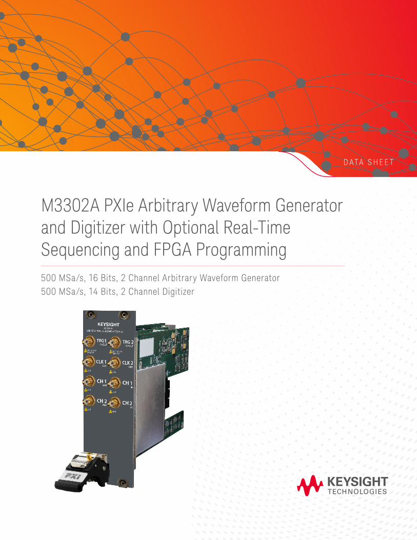
M3302A PXIe Arbitrary Waveform Generator and Digitizer with Optional Real-Time Sequencing and FPGA Programming500 MSa/s, 16 Bits, 2 Channel Arbitrary Waveform Generator500 MSa/s, 14 Bits, 2 Channel Digitizer
Page 2Find us at www.keysight.com
Fast, Flexible, High-Performance Control, Testing and Prototyping
The M3302A combines high-performance arbitrary waveform generator channels and digitizer channels in the same module providing the ideal tool for testing and prototyping in control or communications applications. Performance meets simplicity thanks to easy-to-use programming libraries, real-time sequencing technology (Hard Virtual Instrumentation or HVI), and graphical FPGA programming technology.
Features
Outputs (AWG) – 500 MSa/s, 16 Bits, 2 Channels
Inputs (digitizer) – 500 MSa/s, 14 Bits, 2 Channels
Output features – AWGs, function generators, AM/FM/PM modulators – Advanced triggering and marking functionalities
Input features – Powerful data acquisition system (DAQ) – Advanced triggering and marking functionalities
Less than 400 ns input to output latency
Optional HW programming for high-performance applications – Real-time sequencing (HVI technology) – FPGA programming
– Xilinx Kintex-7K410T FPGA
Up to 2 GB of onboard RAM (~ 1 Gsamples)
Mechanical/interface – 2 slots 3U (PXIe) – PCIe Gen 2 – Independent DMA channels for fast and efficient data transfer
Applications
General purpose AWGs and digitizers
High-performance control
Communications: BB/IF SDR, channel emulation, transceiver testing
Aerospace and defense (A/D): RADAR, electronic warfare (EW)
Hardware-in-the-loop (HIL), automated test equipment (ATE)
Scientific research
Quantum computing
Page 3Find us at www.keysight.com
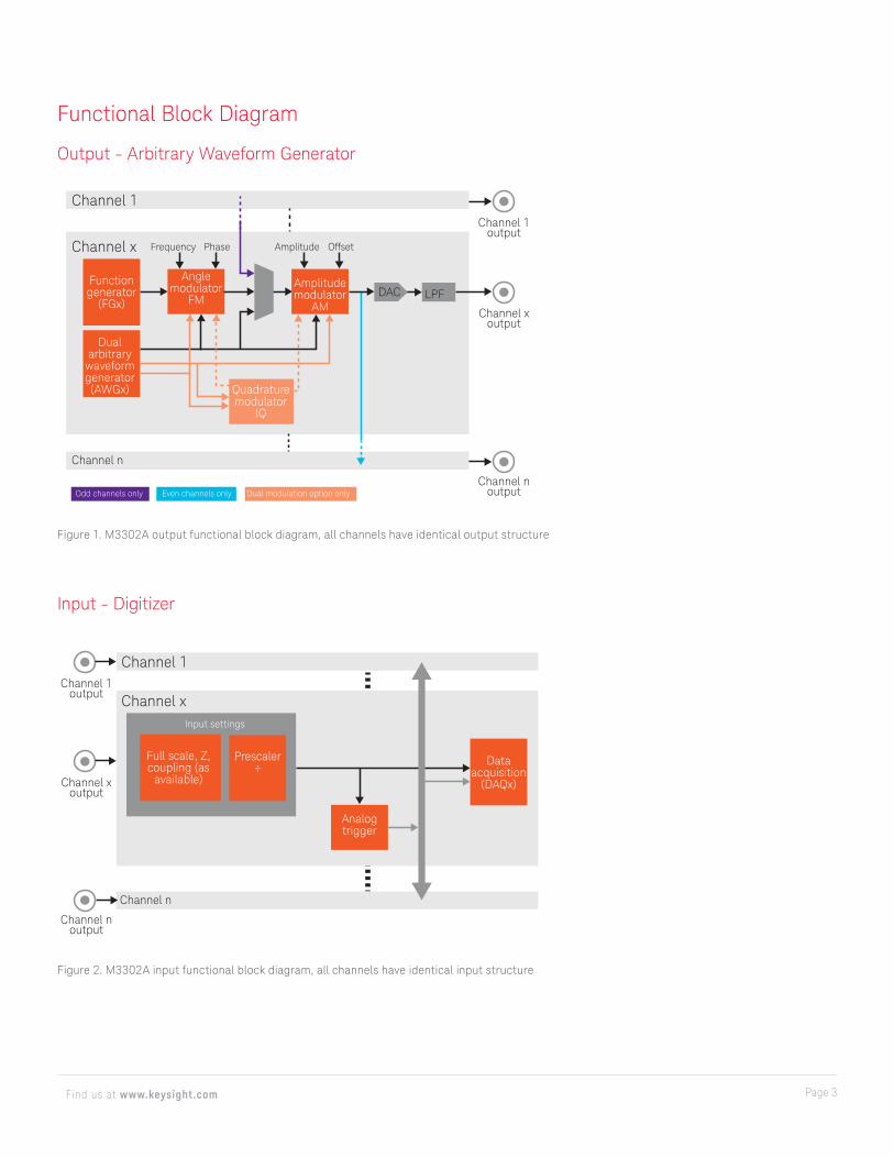
Functional Block Diagram
Output - Arbitrary Waveform Generator
Channel 1
Channel x Amplitude Offset
Channel 1 output
Quadrature modulator
IQ
LPFDAC
Dual arbitrary
waveform generator (AWGx)
Function generator
(FGx)
Angle modulator
FMAmplitude modulator
AM Channel x output
Channel n output
Channel n
Dual modulation option onlyEven channels onlyOdd channels only
PhaseFrequency
Channel 1
Channel xChannel 1
output
Data acquisition
(DAQx)
Full scale, Z, coupling (as
available)
Prescaler÷
Analogtrigger
Channel x output
Channel n
Input settings
Channel n output
Input - Digitizer
Figure 1. M3302A output functional block diagram, all channels have identical output structure
Figure 2. M3302A input functional block diagram, all channels have identical input structure
Page 4Find us at www.keysight.com
Programming Technology and Software Tools
Software programming – Easy-to-use native programming libraries for most common languages: C, C++, Visual
Studio, LabVIEW, MATLAB, Python, and more
Hardware programming (optional) – Real-time sequencing (Hard Virtual Instrumentation or HVI technology)
– Graphical flowchart-style M3601A design environment (-HV1 option required on HW) – Ultra-fast, fully-parallelized, hard real-time execution – Ultra-fast, time-deterministic decision-making – Off-the-shelf inter-module synchronization and data exchange
– FPGA programming – Graphical M3602A FPGA design environment (-FP1 option required on HW) – No FPGA know-how required – Include high-level to low-level design elements: off-the-shelf DSP blocks, MATLAB/
Simulink designs, Xilinx CORE Generator IP cores, Xilinx VIVADO/ISE projects, VHDL or Verilog code
– Ultra-fast, one-click compiling and on-the-fly programming
No programming – Ready-to-use SD1 SPF (software front panels)
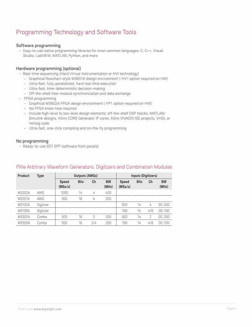
PXIe Arbitrary Waveform Generators, Digitizers and Combination Modules
Product Type Outputs (AWGs) Inputs (Digitizers)
Speed (MSa/s)
Bits Ch BW (MHz)
Speed (MSa/s)
Bits Ch BW (MHz)
M3202A AWG 1000 14 4 400
M3201A AWG 500 16 4 200
M3102A Digitizer 500 14 4 DC-200
M3100A Digitizer 100 14 4/8 DC-100
M3302A Combo 500 16 2 200 500 14 2 DC-200
M3300A Combo 500 16 2/4 200 100 14 4/8 DC-100
Page 5Find us at www.keysight.com
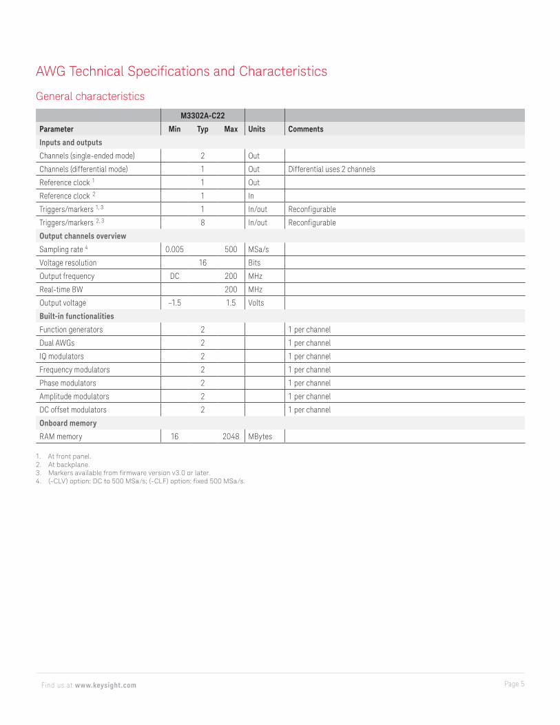
AWG Technical Specifications and Characteristics
General characteristics
M3302A-C22
Parameter Min Typ Max Units Comments
Inputs and outputs
Channels (single-ended mode) 2 Out
Channels (differential mode) 1 Out Differential uses 2 channels
Reference clock 1 1 Out
Reference clock 2 1 In
Triggers/markers 1, 3 1 In/out Reconfigurable
Triggers/markers 2, 3 8 In/out Reconfigurable
Output channels overview
Sampling rate 4 0.005 500 MSa/s
Voltage resolution 16 Bits
Output frequency DC 200 MHz
Real-time BW 200 MHz
Output voltage –1.5 1.5 Volts
Built-in functionalities
Function generators 2 1 per channel
Dual AWGs 2 1 per channel
IQ modulators 2 1 per channel
Frequency modulators 2 1 per channel
Phase modulators 2 1 per channel
Amplitude modulators 2 1 per channel
DC offset modulators 2 1 per channel
Onboard memory
RAM memory 16 2048 MBytes
1. At front panel.2. At backplane.3. Markers available from firmware version v3.0 or later.4. (-CLV) option: DC to 500 MSa/s; (-CLF) option: fixed 500 MSa/s.
Page 6Find us at www.keysight.com
I/O specifications
M3302A-C22
Parameter Min Typ Max Units Comments
Output channels
Sampling rate 1 100 500 MSa/s
Output frequency 0 200 MHz Limited by a reconstruction filter
Output voltage –1.5 1.5 Volts On a 50 Ω load
Source impedance 50 Ω
Reference clock output
Frequency 10 to 12.5 2 MHz Generated from the internal clock, user selectable
Voltage 800 mVpp On a 50 Ω load
Power 2 dBm On a 50 Ω load
Source impedance 50 Ω AC coupled
External I/O trigger/marker
VIH 2 5 V
VIL 0 0.8 V
VOH 2.4 3.3 V On a high Z load
VOL 0 0.25 V On a high Z load
Input impedance 10 KΩ
Source impedance TTL –
Speed 100 MHz
1. (-CLV) option: 100 to 500 MSa/s; (-CLF) option: fixed 500 MSa/s.2. CLF option is set to 10 MHz while with CLV option varies from 12.5 MHz to 10 MHz.
Page 7Find us at www.keysight.com
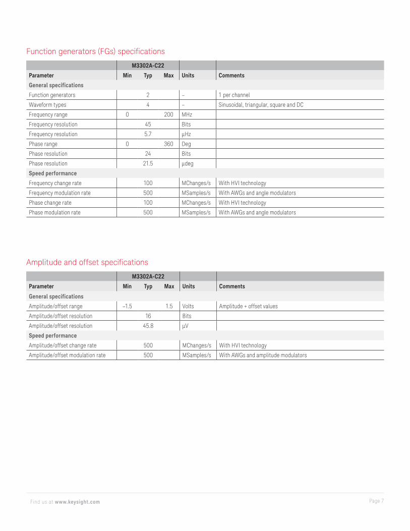
Function generators (FGs) specifications
M3302A-C22
Parameter Min Typ Max Units Comments
General specifications
Function generators 2 – 1 per channel
Waveform types 4 – Sinusoidal, triangular, square and DC
Frequency range 0 200 MHz
Frequency resolution 45 Bits
Frequency resolution 5.7 µHz
Phase range 0 360 Deg
Phase resolution 24 Bits
Phase resolution 21.5 µdeg
Speed performance
Frequency change rate 100 MChanges/s With HVI technology
Frequency modulation rate 500 MSamples/s With AWGs and angle modulators
Phase change rate 100 MChanges/s With HVI technology
Phase modulation rate 500 MSamples/s With AWGs and angle modulators
Amplitude and offset specifications
M3302A-C22
Parameter Min Typ Max Units Comments
General specifications
Amplitude/offset range –1.5 1.5 Volts Amplitude + offset values
Amplitude/offset resolution 16 Bits
Amplitude/offset resolution 45.8 µV
Speed performance
Amplitude/offset change rate 500 MChanges/s With HVI technology
Amplitude/offset modulation rate 500 MSamples/s With AWGs and amplitude modulators
Page 8Find us at www.keysight.com
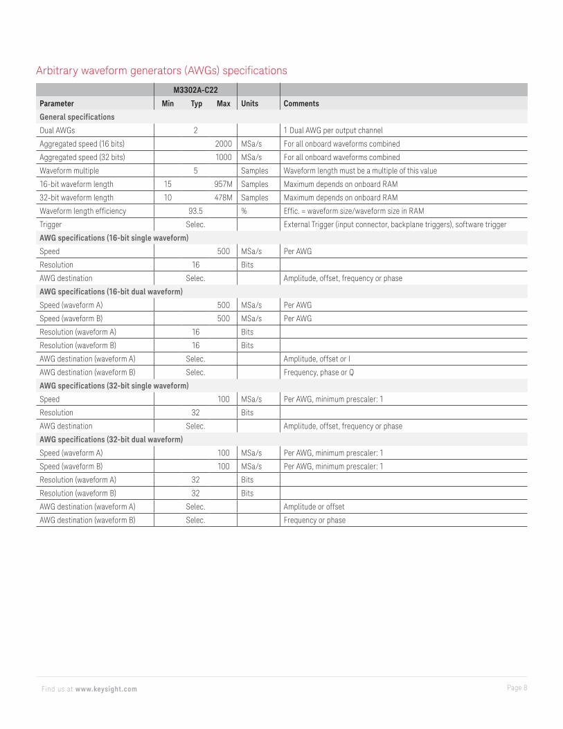
Arbitrary waveform generators (AWGs) specifications
M3302A-C22
Parameter Min Typ Max Units Comments
General specifications
Dual AWGs 2 1 Dual AWG per output channel
Aggregated speed (16 bits) 2000 MSa/s For all onboard waveforms combined
Aggregated speed (32 bits) 1000 MSa/s For all onboard waveforms combined
Waveform multiple 5 Samples Waveform length must be a multiple of this value
16-bit waveform length 15 957M Samples Maximum depends on onboard RAM
32-bit waveform length 10 478M Samples Maximum depends on onboard RAM
Waveform length efficiency 93.5 % Effic. = waveform size/waveform size in RAM
Trigger Selec. External Trigger (input connector, backplane triggers), software trigger
AWG specifications (16-bit single waveform)
Speed 500 MSa/s Per AWG
Resolution 16 Bits
AWG destination Selec. Amplitude, offset, frequency or phase
AWG specifications (16-bit dual waveform)
Speed (waveform A) 500 MSa/s Per AWG
Speed (waveform B) 500 MSa/s Per AWG
Resolution (waveform A) 16 Bits
Resolution (waveform B) 16 Bits
AWG destination (waveform A) Selec. Amplitude, offset or I
AWG destination (waveform B) Selec. Frequency, phase or Q
AWG specifications (32-bit single waveform)
Speed 100 MSa/s Per AWG, minimum prescaler: 1
Resolution 32 Bits
AWG destination Selec. Amplitude, offset, frequency or phase
AWG specifications (32-bit dual waveform)
Speed (waveform A) 100 MSa/s Per AWG, minimum prescaler: 1
Speed (waveform B) 100 MSa/s Per AWG, minimum prescaler: 1
Resolution (waveform A) 32 Bits
Resolution (waveform B) 32 Bits
AWG destination (waveform A) Selec. Amplitude or offset
AWG destination (waveform B) Selec. Frequency or phase
Page 9Find us at www.keysight.com
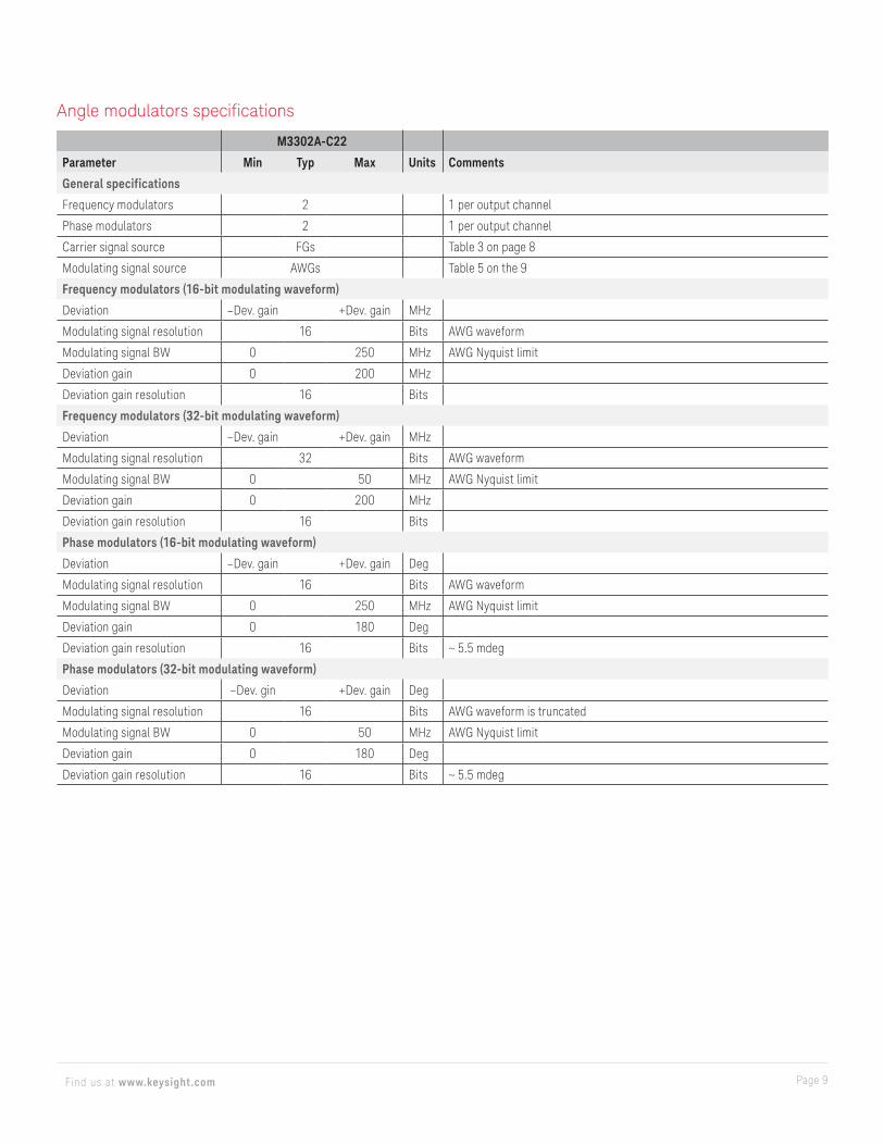
Angle modulators specifications
M3302A-C22
Parameter Min Typ Max Units Comments
General specifications
Frequency modulators 2 1 per output channel
Phase modulators 2 1 per output channel
Carrier signal source FGs Table 3 on page 8
Modulating signal source AWGs Table 5 on the 9
Frequency modulators (16-bit modulating waveform)
Deviation –Dev. gain +Dev. gain MHz
Modulating signal resolution 16 Bits AWG waveform
Modulating signal BW 0 250 MHz AWG Nyquist limit
Deviation gain 0 200 MHz
Deviation gain resolution 16 Bits
Frequency modulators (32-bit modulating waveform)
Deviation –Dev. gain +Dev. gain MHz
Modulating signal resolution 32 Bits AWG waveform
Modulating signal BW 0 50 MHz AWG Nyquist limit
Deviation gain 0 200 MHz
Deviation gain resolution 16 Bits
Phase modulators (16-bit modulating waveform)
Deviation –Dev. gain +Dev. gain Deg
Modulating signal resolution 16 Bits AWG waveform
Modulating signal BW 0 250 MHz AWG Nyquist limit
Deviation gain 0 180 Deg
Deviation gain resolution 16 Bits ~ 5.5 mdeg
Phase modulators (32-bit modulating waveform)
Deviation –Dev. gin +Dev. gain Deg
Modulating signal resolution 16 Bits AWG waveform is truncated
Modulating signal BW 0 50 MHz AWG Nyquist limit
Deviation gain 0 180 Deg
Deviation gain resolution 16 Bits ~ 5.5 mdeg
Page 10Find us at www.keysight.com
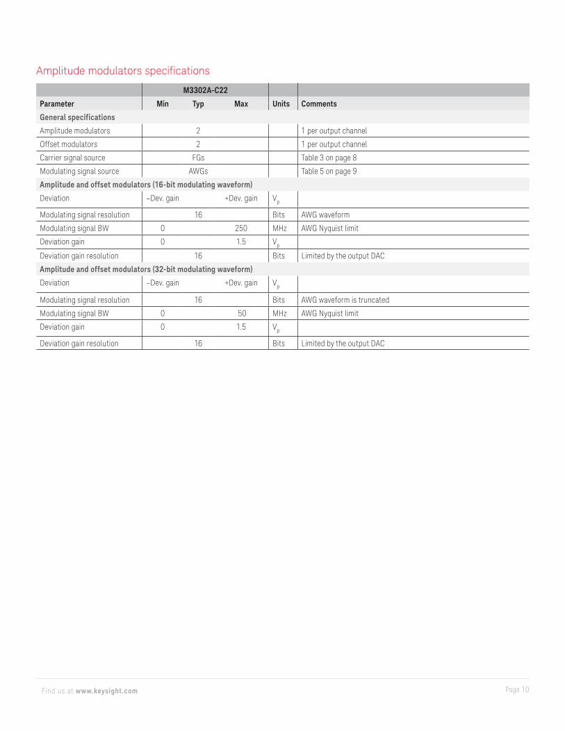
Amplitude modulators specifications
M3302A-C22
Parameter Min Typ Max Units Comments
General specifications
Amplitude modulators 2 1 per output channel
Offset modulators 2 1 per output channel
Carrier signal source FGs Table 3 on page 8
Modulating signal source AWGs Table 5 on page 9
Amplitude and offset modulators (16-bit modulating waveform)
Deviation –Dev. gain +Dev. gain Vp
Modulating signal resolution 16 Bits AWG waveform
Modulating signal BW 0 250 MHz AWG Nyquist limit
Deviation gain 0 1.5 Vp
Deviation gain resolution 16 Bits Limited by the output DAC
Amplitude and offset modulators (32-bit modulating waveform)
Deviation –Dev. gain +Dev. gain Vp
Modulating signal resolution 16 Bits AWG waveform is truncated
Modulating signal BW 0 50 MHz AWG Nyquist limit
Deviation gain 0 1.5 Vp
Deviation gain resolution 16 Bits Limited by the output DAC
Page 11Find us at www.keysight.com
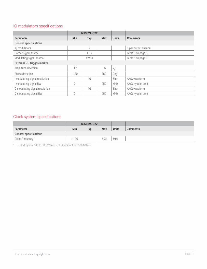
IQ modulators specifications
M3302A-C22
Parameter Min Typ Max Units Comments
General specifications
IQ modulators 2 1 per output channel
Carrier signal source FGs Table 3 on page 8
Modulating signal source AWGs Table 5 on page 9
External I/O trigger/marker
Amplitude deviation −1.5 1.5 Vp
Phase deviation −180 180 Deg
I modulating signal resolution 16 Bits AWG waveform
I modulating signal BW 0 250 MHz AWG Nyquist limit
Q modulating signal resolution 16 Bits AWG waveform
Q modulating signal BW 0 250 MHz AWG Nyquist limit
Clock system specifications
M3302A-C22
Parameter Min Typ Max Units Comments
General specifications
Clock frequency 1 > 100 500 MHz
1. (-CLV) option: 100 to 500 MSa/s; (-CLF) option: fixed 500 MSa/s.
Page 12Find us at www.keysight.com
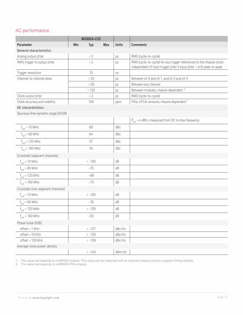
AC performance
M3302A-C22
Parameter Min Typ Max Units Comments
General characteristics
Analog output jitter < 2 ps RMS (cycle-to-cycle)
AWG trigger to output jitter < 2 ps RMS (cycle-to-cycle) for any trigger referenced to the chassis clock; independent of input trigger jitter if input jitter < 4nS peak-to-peak
Trigger resolution 10 ns
Channel-to-channel skew < 20 ps Between ch 0 and ch 1, and ch 2 and ch 3
< 50 ps Between any channel
< 150 ps Between modules, chassis dependant 2
Clock output jitter < 2 ps RMS (cycle-to-cycle)
Clock accuracy and stability 100 ppm PXIe, cPCIe versions; chassis dependent 1
AC characteristics
Spurious-free dynamic range (SFDR)
Pout = 4 dBm, measured from DC to max frequency
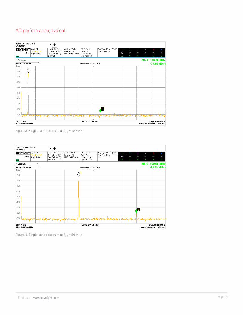
fout = 10 MHz 68 dBc
fout = 80 MHz 64 dBc
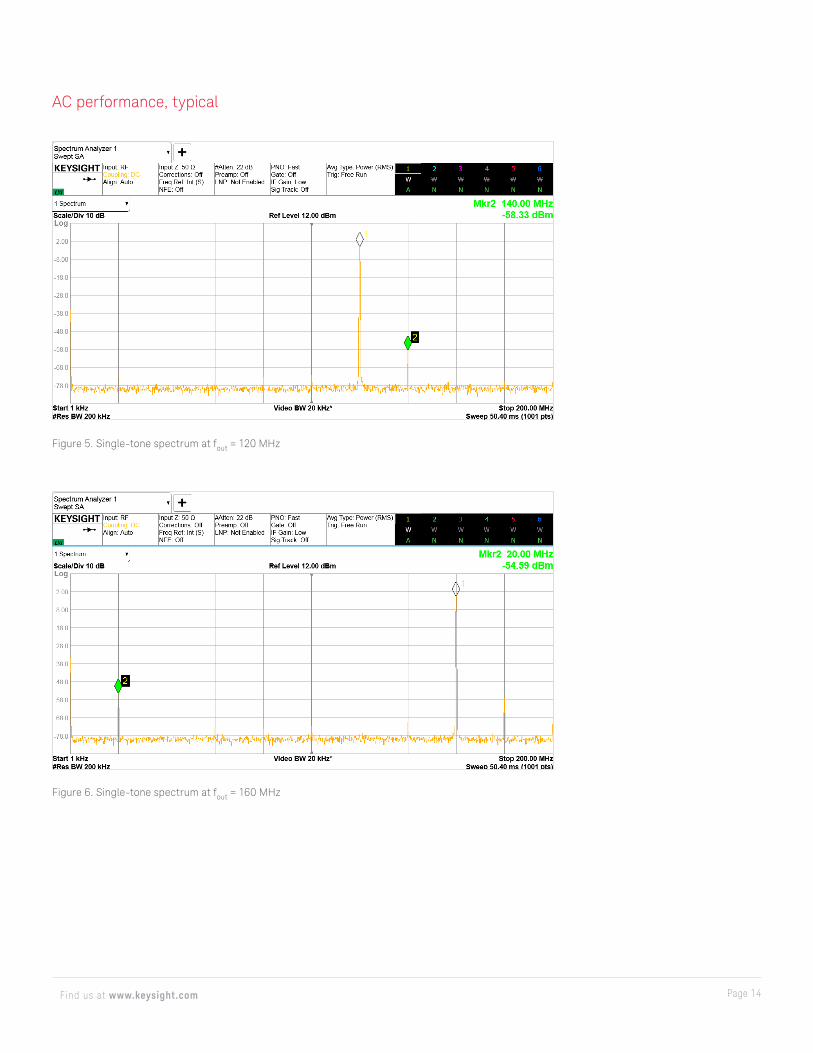
fout = 120 MHz 57 dBc
fout = 160 MHz 54 dBc
Crosstalk (adjacent channels)
fout = 10 MHz < –105 dB
fout = 80 MHz –75 dB
fout = 120 MHz –88 dB
fout = 160 MHz –73 dB
Crosstalk (non-adjacent channels)
fout = 10 MHz < –105 dB
fout = 80 MHz –78 dB
fout = 120 MHz < –105 dB
fout = 160 MHz –92 dB
Phase noise (SSB)
offset = 1 KHz < –127 dBc/Hz
offset = 10 KHz < –133 dBc/Hz
offset = 100 KHz < –138 dBc/Hz
Average noise power density
< –145 dBm/Hz
1. This value corresponds to a M9505A chassis. This value can be improved with an external chassis clock or a system timing module.2. This value corresponds to a M9005A PXIe chassis.
Page 13Find us at www.keysight.com
Figure 3. Single-tone spectrum at fout = 10 MHz
Figure 4. Single-tone spectrum at fout = 80 MHz
AC performance, typical
Page 14Find us at www.keysight.com
Figure 6. Single-tone spectrum at fout = 160 MHz
Figure 5. Single-tone spectrum at fout = 120 MHz
AC performance, typical
Page 15Find us at www.keysight.com
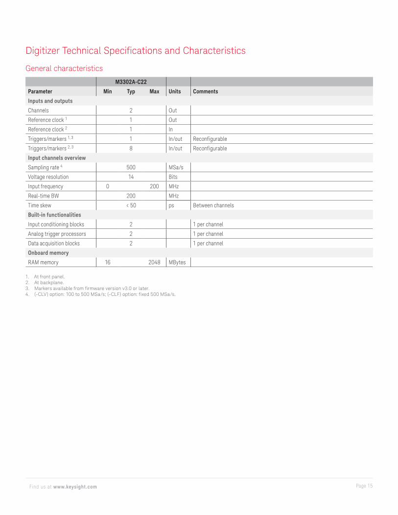
Digitizer Technical Specifications and Characteristics
General characteristics
M3302A-C22
Parameter Min Typ Max Units Comments
Inputs and outputs
Channels 2 Out
Reference clock 1 1 Out
Reference clock 2 1 In
Triggers/markers 1, 3 1 In/out Reconfigurable
Triggers/markers 2, 3 8 In/out Reconfigurable
Input channels overview
Sampling rate 4 500 MSa/s
Voltage resolution 14 Bits
Input frequency 0 200 MHz
Real-time BW 200 MHz
Time skew < 50 ps Between channels
Built-in functionalities
Input conditioning blocks 2 1 per channel
Analog trigger processors 2 1 per channel
Data acquisition blocks 2 1 per channel
Onboard memory
RAM memory 16 2048 MBytes
1. At front panel.2. At backplane.3. Markers available from firmware version v3.0 or later.4. (-CLV) option: 100 to 500 MSa/s; (-CLF) option: fixed 500 MSa/s.
Page 16Find us at www.keysight.com
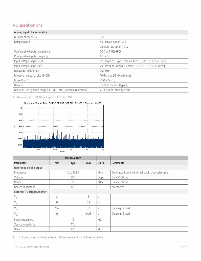
I/O specifications
Analog input characteristics
Number of channels C22
Sampling rate 500 MSa/s option -CLF
Variable rate option -CLV
Configurable inputs: impedance 50 Ω or 1 MΩ (HiZ)
Configurable inputs: Coupling AC or DC
Input voltage range (50 Ω) 125 mVpp to 8 Vpp (7 scales: 0.125, 0.25, 0.5, 1, 2, 4, 8 Vpp)
Input voltage range (HiZ) 200 mVpp to 16 Vpp (7 scales: 0.2, 0.4, 0.8, 2, 4, 8, 16 Vpp)
Bandwidth limit filters 200 MHz
Effective number of bits (ENOB) 1 10.6 bits at 95 MHz (typical)
Noise floor 1 –146 dBm/Hz
SINAD 1 66 dB at 95 MHz (typical)
Spurious free dynamic range (SFDR) + Total Harmonic Distorsion 1 71 dBc at 95 MHz (typical)
1. Measured at –1 DBFS input signal with 1 Vpp 50 Ω.
M3302A-C22
Parameter Min Typ Max Units Comments
Reference clock output
Frequency 10 to 12.5 2 MHz Generated from the internal clock. User selectable
Voltage 800 mVpp On a 50 Ω load
Power 2 dBm On a 50 Ω load
Source impedance 50 Ω AC coupled
External I/O trigger/marker
VIH 2 5 V
VIL 0 0.8 V
VOH 2.4 3.3 V On a high Z load
VOL 0 0.25 V On a high Z load
Input impedance 10 KΩ
Source impedance TTL -
Speed 100 MHz
2. CLF option is set to 10 MHz while with CLV option varies from 12.5 MHz to 10 MHz.
Page 17Find us at www.keysight.com
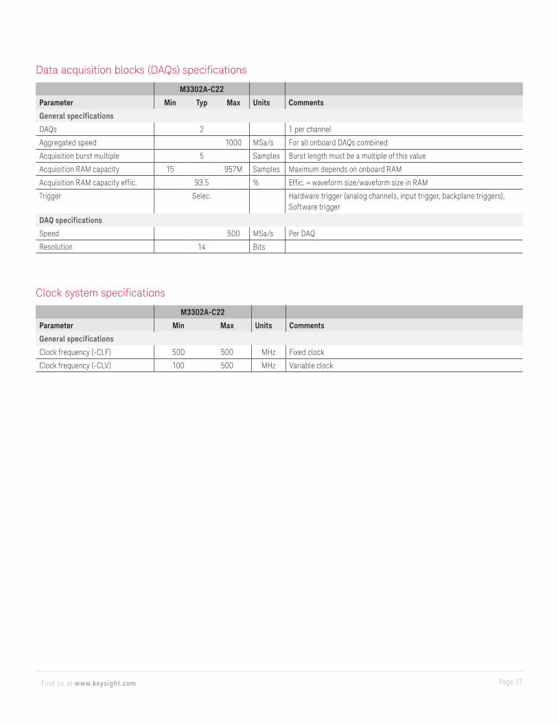
Data acquisition blocks (DAQs) specifications
M3302A-C22
Parameter Min Typ Max Units Comments
General specifications
DAQs 2 1 per channel
Aggregated speed 1000 MSa/s For all onboard DAQs combined
Acquisition burst multiple 5 Samples Burst length must be a multiple of this value
Acquisition RAM capacity 15 957M Samples Maximum depends on onboard RAM
Acquisition RAM capacity effic. 93.5 % Effic. = waveform size/waveform size in RAM
Trigger Selec. Hardware trigger (analog channels, input trigger, backplane triggers), Software trigger
DAQ specifications
Speed 500 MSa/s Per DAQ
Resolution 14 Bits
Clock system specifications
M3302A-C22
Parameter Min Max Units Comments
General specifications
Clock frequency (-CLF) 500 500 MHz Fixed clock
Clock frequency (-CLV) 100 500 MHz Variable clock
Page 18Find us at www.keysight.com
System Specifications
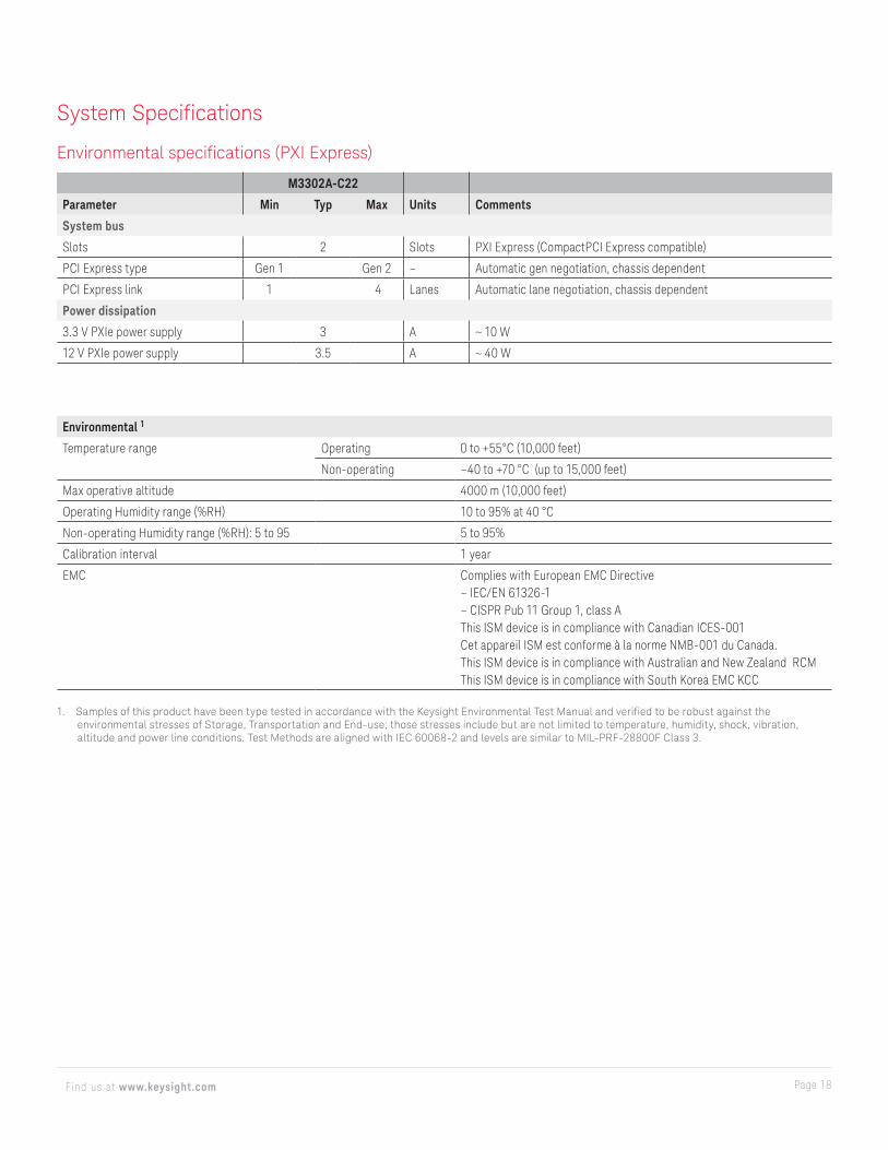
Environmental specifications (PXI Express)
M3302A-C22
Parameter Min Typ Max Units Comments
System bus
Slots 2 Slots PXI Express (CompactPCI Express compatible)
PCI Express type Gen 1 Gen 2 – Automatic gen negotiation, chassis dependent
PCI Express link 1 4 Lanes Automatic lane negotiation, chassis dependent
Power dissipation
3.3 V PXIe power supply 3 A ~ 10 W
12 V PXIe power supply 3.5 A ~ 40 W
Environmental 1
Temperature range Operating 0 to +55°C (10,000 feet)
Non-operating –40 to +70 °C (up to 15,000 feet)
Max operative altitude 4000 m (10,000 feet)
Operating Humidity range (%RH) 10 to 95% at 40 °C
Non-operating Humidity range (%RH): 5 to 95 5 to 95%
Calibration interval 1 year
EMC Complies with European EMC Directive– IEC/EN 61326-1– CISPR Pub 11 Group 1, class AThis ISM device is in compliance with Canadian ICES-001Cet appareil ISM est conforme à la norme NMB-001 du Canada.This ISM device is in compliance with Australian and New Zealand RCMThis ISM device is in compliance with South Korea EMC KCC
1. Samples of this product have been type tested in accordance with the Keysight Environmental Test Manual and verified to be robust against the environmental stresses of Storage, Transportation and End-use; those stresses include but are not limited to temperature, humidity, shock, vibration, altitude and power line conditions. Test Methods are aligned with IEC 60068-2 and levels are similar to MIL-PRF-28800F Class 3.
This information is subject to change without notice. © Keysight Technologies, 2017 - 2020, Published in USA, April 16, 2020, 5992-1808EN
Page 19Find us at www.keysight.com
Learn more at: www.keysight.comFor more information on Keysight Technologies’ products, applications or services,
please contact your local Keysight office. The complete list is available at:
www.keysight.com/find/contactus
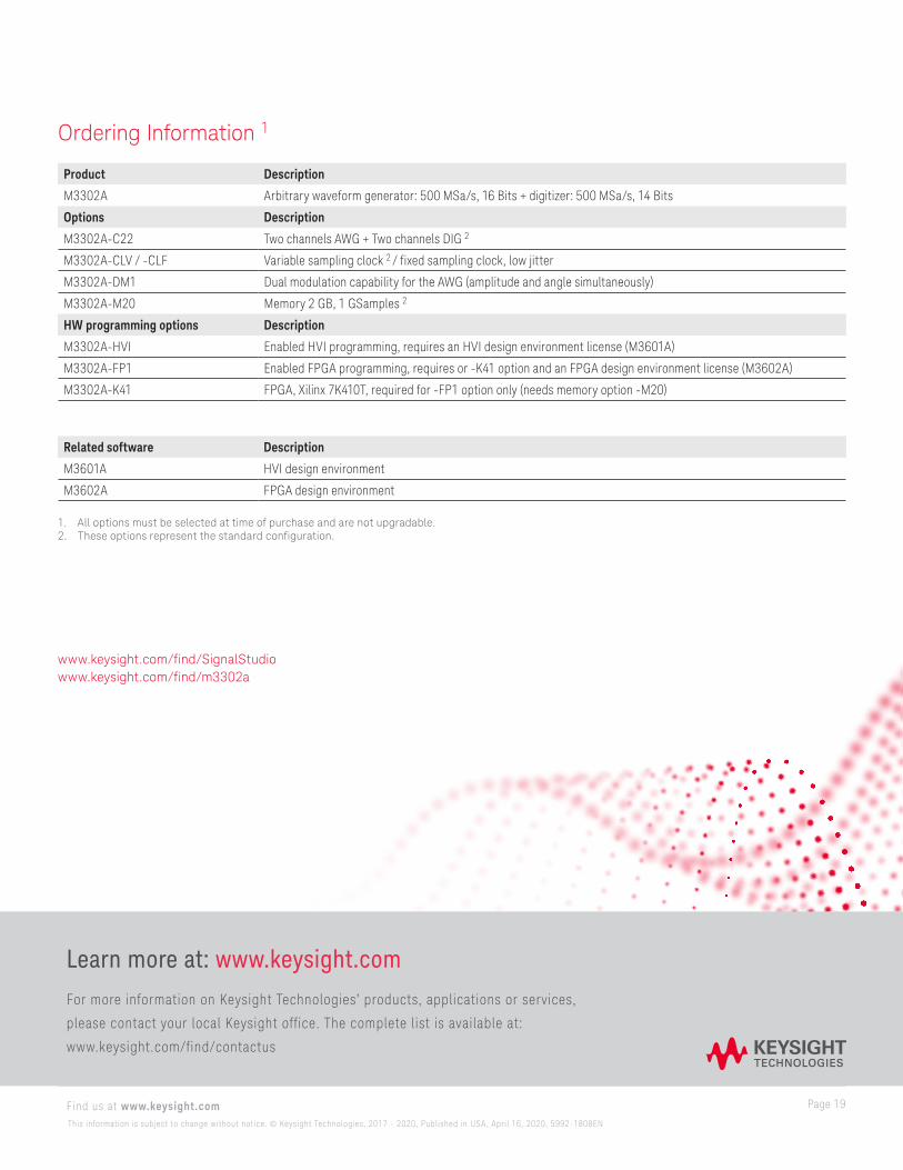
Ordering Information 1
Product Description
M3302A Arbitrary waveform generator: 500 MSa/s, 16 Bits + digitizer: 500 MSa/s, 14 Bits
Options Description
M3302A-C22 Two channels AWG + Two channels DIG 2
M3302A-CLV / -CLF Variable sampling clock 2 / fixed sampling clock, low jitter
M3302A-DM1 Dual modulation capability for the AWG (amplitude and angle simultaneously)
M3302A-M20 Memory 2 GB, 1 GSamples 2
HW programming options Description
M3302A-HVI Enabled HVI programming, requires an HVI design environment license (M3601A)
M3302A-FP1 Enabled FPGA programming, requires or -K41 option and an FPGA design environment license (M3602A)
M3302A-K41 FPGA, Xilinx 7K410T, required for -FP1 option only (needs memory option -M20)
Related software Description
M3601A HVI design environment
M3602A FPGA design environment
1. All options must be selected at time of purchase and are not upgradable.2. These options represent the standard configuration.
www.keysight.com/find/SignalStudiowww.keysight.com/find/m3302a