ltc3331 - nanopower buck-boost dc/dc with energy ... · pdf filenanopower buck-boost dc/dc...
TRANSCRIPT
LTC3331
13331fa
For more information www.linear.com/LTC3331
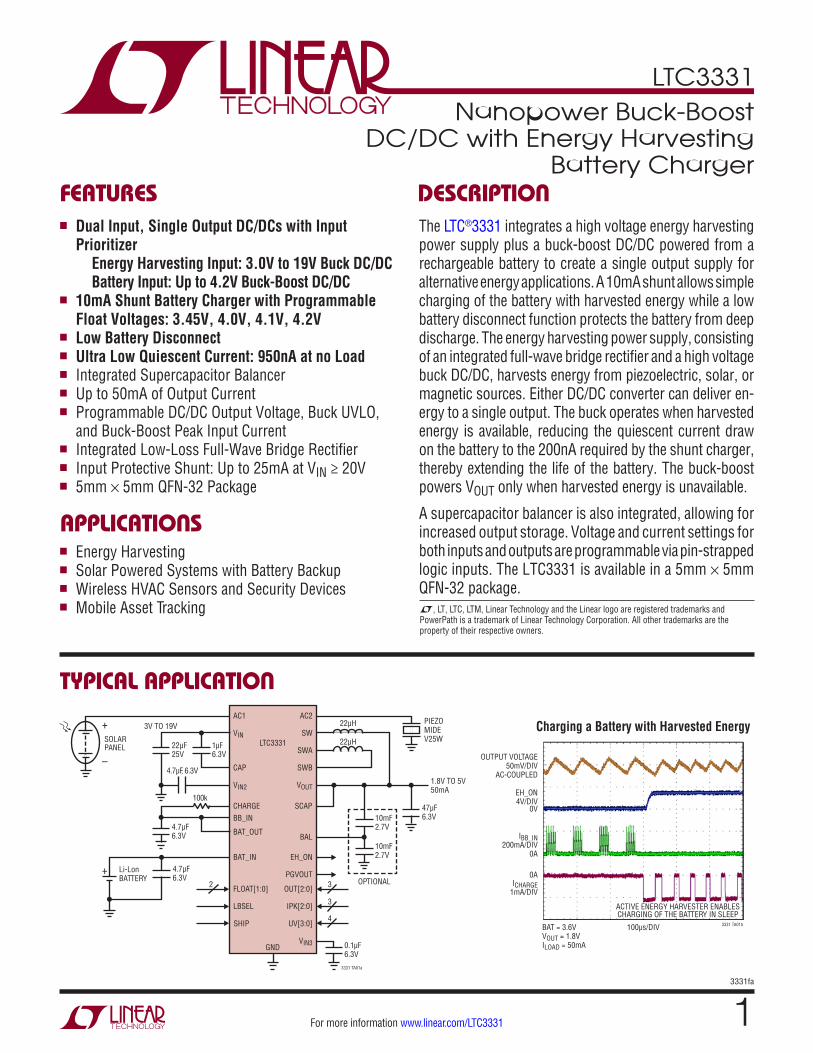
TYPICAL APPLICATION
FEATURES DESCRIPTION
Nanopower Buck-Boost DC/DC with Energy Harvesting
Battery Charger
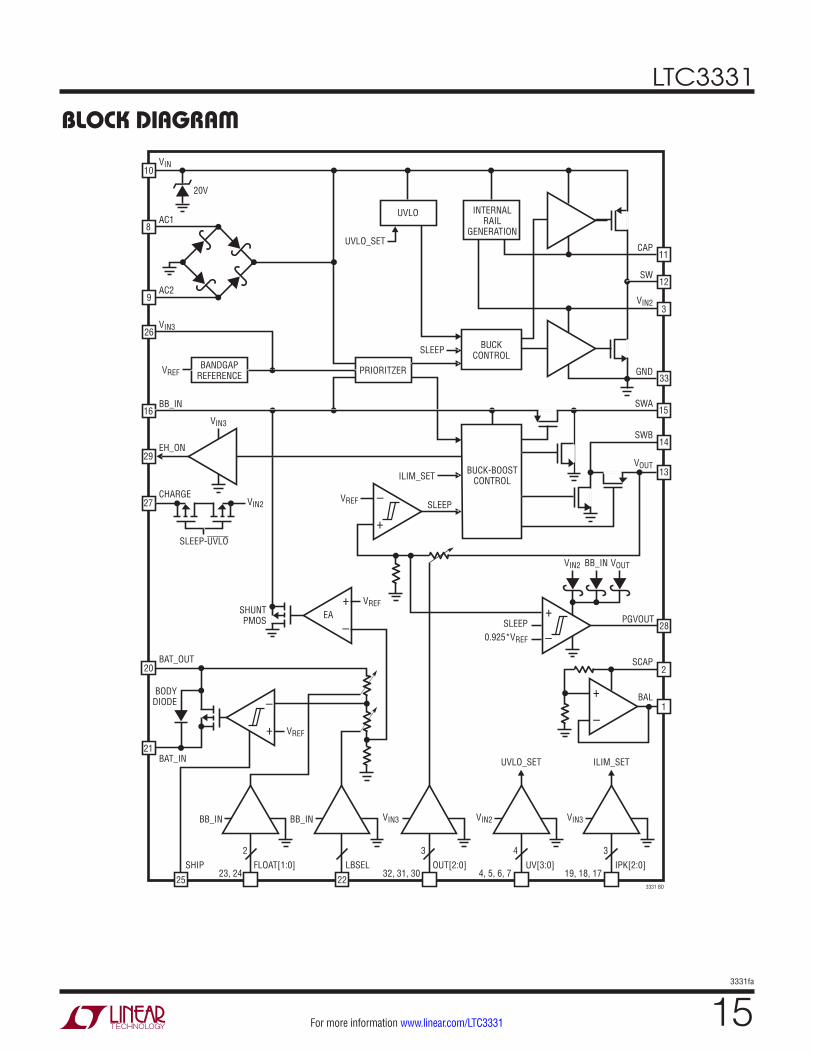
The LTC®3331 integrates a high voltage energy harvesting power supply plus a buck-boost DC/DC powered from a rechargeable battery to create a single output supply for alternative energy applications. A 10mA shunt allows simple charging of the battery with harvested energy while a low battery disconnect function protects the battery from deep discharge. The energy harvesting power supply, consisting of an integrated full-wave bridge rectifier and a high voltage buck DC/DC, harvests energy from piezoelectric, solar, or magnetic sources. Either DC/DC converter can deliver en-ergy to a single output. The buck operates when harvested energy is available, reducing the quiescent current draw on the battery to the 200nA required by the shunt charger, thereby extending the life of the battery. The buck-boost powers VOUT only when harvested energy is unavailable.
A supercapacitor balancer is also integrated, allowing for increased output storage. Voltage and current settings for both inputs and outputs are programmable via pin-strapped logic inputs. The LTC3331 is available in a 5mm × 5mm QFN-32 package.
APPLICATIONS
n Dual Input, Single Output DC/DCs with Input Prioritizer Energy Harvesting Input: 3.0V to 19V Buck DC/DC
Battery Input: Up to 4.2V Buck-Boost DC/DCn 10mA Shunt Battery Charger with Programmable
Float Voltages: 3.45V, 4.0V, 4.1V, 4.2Vn Low Battery Disconnectn Ultra Low Quiescent Current: 950nA at no Loadn Integrated Supercapacitor Balancern Up to 50mA of Output Currentn Programmable DC/DC Output Voltage, Buck UVLO,
and Buck-Boost Peak Input Currentn Integrated Low-Loss Full-Wave Bridge Rectifiern Input Protective Shunt: Up to 25mA at VIN ≥ 20Vn 5mm × 5mm QFN-32 Package
n Energy Harvestingn Solar Powered Systems with Battery Backupn Wireless HVAC Sensors and Security Devicesn Mobile Asset Tracking L, LT, LTC, LTM, Linear Technology and the Linear logo are registered trademarks and
PowerPath is a trademark of Linear Technology Corporation. All other trademarks are the property of their respective owners.
PIEZOMIDEV25W
1µF6.3V
4.7µF, 6.3V
100k
GND
LTC3331
3331 TA01a
AC1
VIN
CAP
CHARGE
VIN2
BAT_IN
BAT_OUT
BB_IN
FLOAT[1:0]
LBSEL
AC2
SW
SWA
22µH
22µH
SWB
VOUT
SCAP
BAL
SHIP
EH_ON
PGVOUT
IPK[2:0]
OUT[2:0]
UV[3:0]
VIN3
3V TO 19V
SOLARPANEL
4.7µF6.3V
4.7µF6.3V
Li-LonBATTERY
22µF25V
2 3
3
4
+
0.1µF6.3V
1.8V TO 5V50mA
10mF2.7V
10mF2.7V
OPTIONAL
47µF6.3V
+
– OUTPUT VOLTAGE50mV/DIV
AC-COUPLED
EH_ON4V/DIV
IBB_IN200mA/DIV
ICHARGE1mA/DIV
0A
0A
0V
100µs/DIV
ACTIVE ENERGY HARVESTER ENABLESCHARGING OF THE BATTERY IN SLEEP
3331 TA01bBAT = 3.6VVOUT = 1.8VILOAD = 50mA
Charging a Battery with Harvested Energy
LTC3331
23331fa
For more information www.linear.com/LTC3331
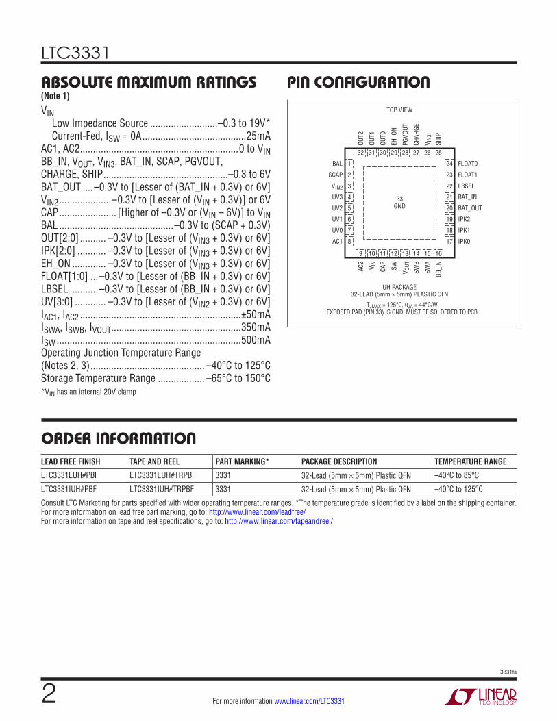
PIN CONFIGURATIONABSOLUTE MAXIMUM RATINGS
VIN Low Impedance Source ..........................–0.3 to 19V* Current-Fed, ISW = 0A ........................................25mA
AC1, AC2 .............................................................0 to VINBB_IN, VOUT, VIN3, BAT_IN, SCAP, PGVOUT, CHARGE, SHIP ................................................–0.3 to 6VBAT_OUT ....–0.3V to [Lesser of (BAT_IN + 0.3V) or 6V]VIN2 ....................–0.3V to [Lesser of (VIN + 0.3V)] or 6VCAP ...................... [Higher of –0.3V or (VIN – 6V)] to VINBAL ............................................–0.3V to (SCAP + 0.3V)OUT[2:0] .......... –0.3V to [Lesser of (VIN3 + 0.3V) or 6V]IPK[2:0] ........... –0.3V to [Lesser of (VIN3 + 0.3V) or 6V]EH_ON ............. –0.3V to [Lesser of (VIN3 + 0.3V) or 6V]FLOAT[1:0] ...–0.3V to [Lesser of (BB_IN + 0.3V) or 6V]LBSEL ...........–0.3V to [Lesser of (BB_IN + 0.3V) or 6V]UV[3:0] ............ –0.3V to [Lesser of (VIN2 + 0.3V) or 6V] IAC1, IAC2 ..............................................................±50mAISWA, ISWB, IVOUT..................................................350mAISW .......................................................................500mAOperating Junction Temperature Range (Notes 2, 3) ............................................ –40°C to 125°CStorage Temperature Range .................. –65°C to 150°C*VIN has an internal 20V clamp
(Note 1)
32
33GND
31 30 29 28 27 26 25
9 10 11 12
TOP VIEW
UH PACKAGE32-LEAD (5mm × 5mm) PLASTIC QFN
13 14 15 16
17
18
19
20
21
22
23
24
8
7
6
5
4
3
2
1BAL
SCAP
VIN2
UV3
UV2
UV1
UV0
AC1
FLOAT0
FLOAT1
LBSEL
BAT_IN
BAT_OUT
IPK2
IPK1
IPK0
OUT2
OUT1
OUT0
EH_O
N
PGVO
UT
CHAR
GE
V IN3
SHIP
AC2
V IN
CAP
SW
V OUT
SWB
SWA
BB_I
N
TJMAX = 125°C, θJA = 44°C/W
EXPOSED PAD (PIN 33) IS GND, MUST BE SOLDERED TO PCB
ORDER INFORMATIONLEAD FREE FINISH TAPE AND REEL PART MARKING* PACKAGE DESCRIPTION TEMPERATURE RANGE
LTC3331EUH#PBF LTC3331EUH#TRPBF 3331 32-Lead (5mm × 5mm) Plastic QFN –40°C to 85°C
LTC3331IUH#PBF LTC3331IUH#TRPBF 3331 32-Lead (5mm × 5mm) Plastic QFN –40°C to 125°C
Consult LTC Marketing for parts specified with wider operating temperature ranges. *The temperature grade is identified by a label on the shipping container.For more information on lead free part marking, go to: http://www.linear.com/leadfree/ For more information on tape and reel specifications, go to: http://www.linear.com/tapeandreel/
LTC3331
33331fa
For more information www.linear.com/LTC3331
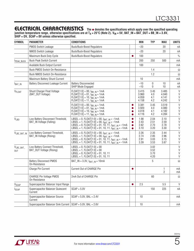
ELECTRICAL CHARACTERISTICS
SYMBOL PARAMETER CONDITIONS MIN TYP MAX UNITS
VIN Buck Input Voltage Range l 19 V
VBB_IN Buck-Boost Input Voltage Range (Note 7) l 1.8 5.5 V
IVIN VIN Quiescent Current VIN Input in UVLO VIN Input in UVLO Buck Enabled, Sleeping Buck Enabled, Sleeping Buck Enabled, Not Sleeping
VIN = 2.5V, VBB_IN = 0V VIN = 16V, VBB_IN = 0V VIN = 4V, VBB_IN = 0V VIN = 18V, VBB_IN = 0V VIN = 5V, VBB_IN = 0V, ISW = 0A (Note 4)
450 800
1300 1800 150
700
1400 2000 2700 225
nA nA nA nA µA
IBB_IN BB_IN Quiescent Current (Note 6) BB_IN Input with VIN Active Buck-Boost Enabled, Sleeping Buck-Boost Enabled, Not Sleeping
VBB_IN = 3.6V, VIN = 5V VBB_IN = 3.6V, VIN = 0V VBB_IN = 3.6V, VIN = 0V, ISWA = ISWB = 0A (Note 4)
200 950 200
300
1500 300
nA nA µA
IVOUT VOUT Leakage Current 5V Output Selected, Sleeping 100 150 nA
VIN Undervoltage Lockout Thresholds (Rising or Falling)
3V Level Selected l 2.91 3.00 3.09 V
4V Level Selected l 3.88 4.00 4.12 V
5V Level Selected l 4.85 5.00 5.15 V
6V Level Selected l 5.82 6.00 6.18 V
7V Level Selected l 6.79 7.00 7.21 V
8V Level Selected l 7.76 8.00 8.24 V
9V Level Selected l 8.73 9.00 9.27 V
10V Level Selected l 9.70 10.0 10.30 V
11V Level Selected l 10.67 11.0 11.33 V
12V Level Selected l 11.64 12.0 12.36 V
13V Level Selected l 12.61 13.0 13.39 V
14V Level Selected l 13.58 14.0 14.42 V
15V Level Selected l 14.55 15.0 15.45 V
16V Level Selected l 15.52 16.0 16.48 V
17V Level Selected l 16.49 17.0 17.51 V
18V Level Selected l 17.46 18.0 18.54 V
VSHUNT VIN Shunt Regulator Voltage IVIN = 1mA l 19.0 20.0 21.0 V
ISHUNT Maximum Protective Shunt Current 25 mA
Internal Bridge Rectifier Loss (|VAC1 – VAC2| – VIN)
IBRIDGE = 10µA IBRIDGE = 50mA
700 1350
800 1550
900 1750
mV mV
Internal Bridge Rectifier Reverse Leakage Current
VREVERSE = 18V 20 nA
Internal Bridge Rectifier Reverse Breakdown Voltage
IREVERSE = 1µA VSHUNT 30 V
The l denotes the specifications which apply over the specified operating junction temperature range, otherwise specifications are at TA = 25°C (Note 2). VIN = 5V, BAT_IN = BAT_OUT = BB_IN = 3.6V, SHIP = OV, SCAP = 0V unless otherwise specified.
LTC3331
43331fa
For more information www.linear.com/LTC3331
SYMBOL PARAMETER CONDITIONS MIN TYP MAX UNITS
VOUT Regulated Buck/Buck-Boost Output Voltage
1.8V Output Selected Sleep Threshold Wake-Up Threshold
l
l
1.728
1.806 1.794
1.872
V V
2.5V Output Selected Sleep Threshold Wake-Up Threshold
l
l
2.425
2.508 2.492
2.575
V V
2.8V Output Selected Sleep Threshold Wake-Up Threshold
l
l
2.716
2.809 2.791
2.884
V V
3.0V Output Selected Sleep Threshold Wake-Up Threshold
l
l
2.910
3.010 2.990
3.090
V V
3.3V Output Selected Sleep Threshold Wake-Up Threshold
l
l
3.200
3.311 3.289
3.400
V V
3.6V Output Selected Sleep Threshold Wake-Up Threshold
l
l
3.492
3.612 3.588
3.708
V V
4.5V Output Selected Sleep Threshold Wake-Up Threshold
l
l
4.365
4.515 4.485
4.635
V V
5.0V Output Selected Sleep Threshold Wake-Up Threshold
l
l
4.850
5.017 4.983
5.150
V V
PGVOUT Falling Threshold As a Percentage of VOUT Target (Note 5) l 88 92 96 %
IPEAK_BB Buck-Boost Peak Switch Current 250mA Target Selected 200 250 350 mA
150mA Target Selected 120 150 210 mA
100mA Target Selected 80 100 140 mA
50mA Target Selected 40 50 70 mA
25mA Target Selected 20 25 35 mA
15mA Target Selected 12 15 21 mA
10mA Target Selected 8 10 14 mA
5mA Target Selected 4 5 7 mA
Available Buck-Boost Current IPEAK_BB = 250mA 50 mA
Buck-Boost PMOS Input and Output Switch On-Resistance
IPK[2:0] = 111 IPK[2:0] = 110 IPK[2:0] = 101 IPK[2:0] = 100 IPK[2:0] = 011 IPK[2:0] = 010 IPK[2:0] = 001 IPK[2:0] = 000
0.8 1.0 1.4 2.4 4.5 7.3
10.7 20.5
Ω Ω Ω Ω Ω Ω Ω Ω
Buck-Boost NMOS Input and Output Switch On-Resistance
IPK2 = 1 IPK2 = 0
0.6 3.9
Ω Ω
ELECTRICAL CHARACTERISTICS The l denotes the specifications which apply over the specified operating junction temperature range, otherwise specifications are at TA = 25°C (Note 2). VIN = 5V, BAT_IN = BAT_OUT = BB_IN = 3.6V, SHIP = OV, SCAP = 0V unless otherwise specified.
LTC3331
53331fa
For more information www.linear.com/LTC3331
ELECTRICAL CHARACTERISTICS The l denotes the specifications which apply over the specified operating junction temperature range, otherwise specifications are at TA = 25°C (Note 2). VIN = 5V, BAT_IN = BAT_OUT = BB_IN = 3.6V, SHIP = OV, SCAP = 0V unless otherwise specified.
SYMBOL PARAMETER CONDITIONS MIN TYP MAX UNITS
PMOS Switch Leakage Buck/Buck-Boost Regulators –20 20 nA
NMOS Switch Leakage Buck/Buck-Boost Regulators –20 20 nA
Maximum Buck Duty Cycle Buck/Buck-Boost Regulators l 100 %
IPEAK_BUCK Buck Peak Switch Current 200 250 500 mA
Available Buck Output Current 100 mA
Buck PMOS Switch On-Resistance 1.4 Ω
Buck NMOS Switch On-Resistance 1.2 Ω
Maximum Battery Shunt Current 10 mA
IBAT_IN Battery Disconnect Leakage Current Battery Disconnected SHIP Mode Engaged
–10 –10
0 0
10 10
nA nA
VFLOAT Shunt Charger Float Voltage (BAT_OUT Voltage)
FLOAT[1:0] = 00, IBB_IN = 1mA FLOAT[1:0] = 01, IBB_IN = 1mA FLOAT[1:0] = 10, IBB_IN = 1mA FLOAT[1:0] = 11, IBB_IN = 1mA
3.415 3.960 4.059 4.158
3.45 4.0 4.1 4.2
3.485 4.040 4.141 4.242
V V V V
FLOAT[1:0] = 00, IBB_IN = 1mA FLOAT[1:0] = 01, IBB_IN = 1mA FLOAT[1:0] = 10, IBB_IN = 1mA FLOAT[1:0] = 11, IBB_IN = 1mA
l
l
l
l
3.381 3.920 4.018 4.116
3.45 4.0 4.1 4.2
3.519 4.080 4.182 4.284
V V V V
VLBD Low Battery Disconnect Threshold, BAT_IN Voltage (Falling)
LBSEL = 0, FLOAT[1:0] = 00, IBAT_IN = –1mA LBSEL = 1, FLOAT[1:0] = 00, IBAT_IN = –1mA LBSEL = 0, FLOAT[1:0] = 01, 10, 11, IBAT_IN = –1mA LBSEL = 1, FLOAT[1:0] = 01, 10, 11, IBAT_IN = –1mA
l
l
l
l
1.98 2.43 2.62 3.10
2.04 2.51 2.70 3.20
2.10 2.59 2.78 3.30
V V V V
VLBC_BAT_IN Low Battery Connect Threshold, BAT_IN Voltage (Rising)
LBSEL = 0, FLOAT[1:0] = 00, IBAT_IN = –1mA LBSEL = 1, FLOAT[1:0] = 00, IBAT_IN = –1mA LBSEL = 0, FLOAT[1:0] = 01, 10, 11, IBAT_IN = –1mA LBSEL = 1, FLOAT[1:0] = 01, 10, 11, IBAT_IN = –1mA
2.26 2.74 2.91 3.39
2.35 2.85 3.03 3.53
2.44 2.96 3.15 3.67
V V V V
VLBC_BAT_OUT
Low Battery Connect Threshold, BAT_OUT Voltage (Rising)
LBSEL = 0, FLOAT[1:0] = 00 LBSEL = 1, FLOAT[1:0] = 00 LBSEL = 0, FLOAT[1:0] = 01, 10, 11 LBSEL = 1, FLOAT[1:0] = 01, 10, 11
3.02 3.52 3.70 4.20
V V V V
Battery Disconnect PMOS On-Resistance
BAT_IN = 3.3V, IBAT_IN = 10mA 5 Ω
Charge Pin Current Current Out of CHARGE Pin l 1 2
mA mA
CHARGE Pin Voltage PMOS On-Resistance
2mA Out of CHARGE Pin 60 Ω
VSCAP Supercapacitor Balancer Input Range l 2.5 5.5 V
ISCAP Supercapacitor Balancer Quiescent Current
SCAP = 5.0V 150 225 nA
Supercapacitor Balancer Source Current
SCAP = 5.0V, BAL = 2.4V 10 mA
Supercapacitor Balancer Sink Current SCAP = 5.0V, BAL = 2.6V 10 mA
LTC3331
63331fa
For more information www.linear.com/LTC3331
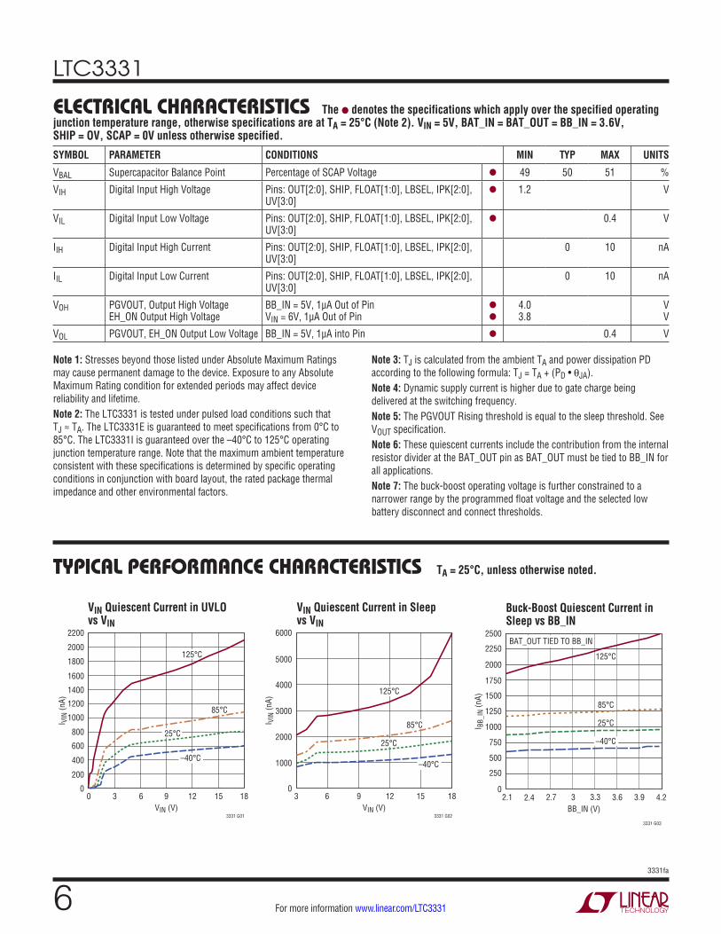
TYPICAL PERFORMANCE CHARACTERISTICS
VIN Quiescent Current in UVLO vs VIN
VIN Quiescent Current in Sleep vs VIN
Buck-Boost Quiescent Current in Sleep vs BB_IN
VIN (V)0
I VIN
(nA)
2200
2000
1600
1200
1800
1400
1000
800
600
400
200
096 15
3331 G01
183 12
125°C
85°C
25°C
–40°C
BB_IN (V)2.1
0
I BB_
IN (n
A)
250
750
1000
1250
2500
1750
2.7 3.3 3.6 3.9
3331 G03
500
2000125°C
85°C
25°C
2250
1500
2.4 3 4.2
–40°C
BAT_OUT TIED TO BB_IN
TA = 25°C, unless otherwise noted.
VIN (V)
I VIN
(nA)
6000
5000
4000
3000
2000
1000
096 15
3331 G02
183 12
125°C
–40°C
85°C
25°C
ELECTRICAL CHARACTERISTICS The l denotes the specifications which apply over the specified operating junction temperature range, otherwise specifications are at TA = 25°C (Note 2). VIN = 5V, BAT_IN = BAT_OUT = BB_IN = 3.6V, SHIP = OV, SCAP = 0V unless otherwise specified.
Note 1: Stresses beyond those listed under Absolute Maximum Ratings may cause permanent damage to the device. Exposure to any Absolute Maximum Rating condition for extended periods may affect device reliability and lifetime.Note 2: The LTC3331 is tested under pulsed load conditions such that TJ ≈ TA. The LTC3331E is guaranteed to meet specifications from 0°C to 85°C. The LTC3331I is guaranteed over the –40°C to 125°C operating junction temperature range. Note that the maximum ambient temperature consistent with these specifications is determined by specific operating conditions in conjunction with board layout, the rated package thermal impedance and other environmental factors.
Note 3: TJ is calculated from the ambient TA and power dissipation PD according to the following formula: TJ = TA + (PD • θJA).Note 4: Dynamic supply current is higher due to gate charge being delivered at the switching frequency. Note 5: The PGVOUT Rising threshold is equal to the sleep threshold. See VOUT specification.Note 6: These quiescent currents include the contribution from the internal resistor divider at the BAT_OUT pin as BAT_OUT must be tied to BB_IN for all applications.Note 7: The buck-boost operating voltage is further constrained to a narrower range by the programmed float voltage and the selected low battery disconnect and connect thresholds.
SYMBOL PARAMETER CONDITIONS MIN TYP MAX UNITS
VBAL Supercapacitor Balance Point Percentage of SCAP Voltage l 49 50 51 %
VIH Digital Input High Voltage Pins: OUT[2:0], SHIP, FLOAT[1:0], LBSEL, IPK[2:0], UV[3:0]
l 1.2 V
VIL Digital Input Low Voltage Pins: OUT[2:0], SHIP, FLOAT[1:0], LBSEL, IPK[2:0], UV[3:0]
l 0.4 V
IIH Digital Input High Current Pins: OUT[2:0], SHIP, FLOAT[1:0], LBSEL, IPK[2:0], UV[3:0]
0 10 nA
IIL Digital Input Low Current Pins: OUT[2:0], SHIP, FLOAT[1:0], LBSEL, IPK[2:0], UV[3:0]
0 10 nA
VOH PGVOUT, Output High Voltage EH_ON Output High Voltage
BB_IN = 5V, 1µA Out of Pin VIN = 6V, 1µA Out of Pin
l
l
4.0 3.8
V V
VOL PGVOUT, EH_ON Output Low Voltage BB_IN = 5V, 1µA into Pin l 0.4 V
LTC3331
73331fa
For more information www.linear.com/LTC3331
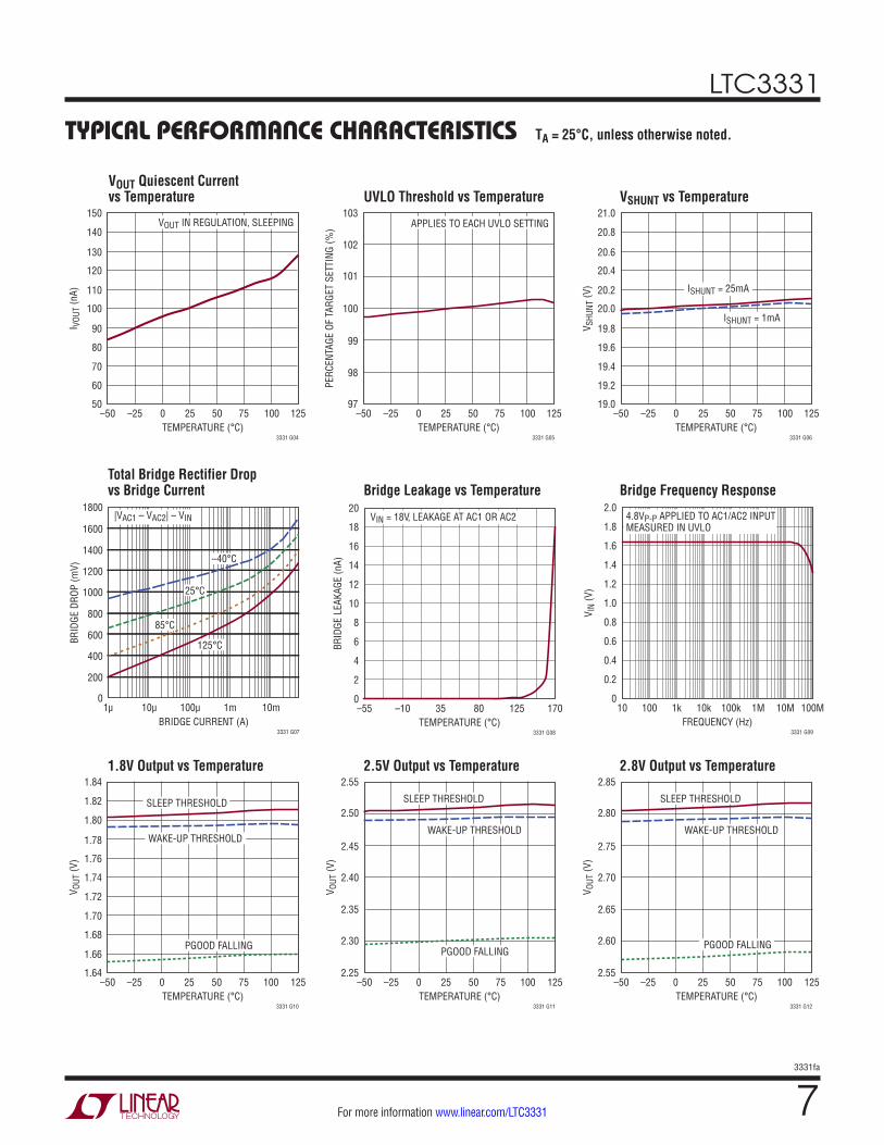
TYPICAL PERFORMANCE CHARACTERISTICS
UVLO Threshold vs Temperature VSHUNT vs TemperatureVOUT Quiescent Current vs Temperature
Total Bridge Rectifier Drop vs Bridge Current Bridge Leakage vs Temperature Bridge Frequency Response
BRIDGE CURRENT (A)
BRID
GE D
ROP
(mV)
1800
1600
1400
1200
1000
800
600
400
200
0
3331 G07
1µ 10µ 10m1m100µ
–40°C
25°C
85°C
125°C
|VAC1 – VAC2| – VIN
FREQUENCY (Hz)
V IN
(V)
3331 G09
2.0
1.8
1.6
1.4
1.2
1.0
0.8
0.6
0.4
0.2
010 100 100M10M1M10k1k 100k
4.8VP-P APPLIED TO AC1/AC2 INPUTMEASURED IN UVLO
TA = 25°C, unless otherwise noted.
TEMPERATURE (°C)–55
BRID
GE L
EAKA
GE (n
A)
20
18
14
10
16
12
6
8
4
2
08035 125
3331 G08
170–10
VIN = 18V, LEAKAGE AT AC1 OR AC2
TEMPERATURE (°C)–50
I VOU
T (n
A)
150
140
130
120
110
100
90
80
60
70
500 25 50 75 100
3331 G04
125–25
VOUT IN REGULATION, SLEEPING
TEMPERATURE (°C)–50
PERC
ENTA
GE O
F TA
RGET
SET
TING
(%)
103
102
101
100
99
98
970 25 50 75 100
3331 G05
125–25
APPLIES TO EACH UVLO SETTING
TEMPERATURE (°C)–50
V SHU
NT (V
)
21.0
20.8
20.6
20.4
20.2
20.0
19.8
19.6
19.2
19.4
19.00 25 50 75 100
3331 G06
125–25
ISHUNT = 1mA
ISHUNT = 25mA
1.8V Output vs Temperature 2.5V Output vs Temperature 2.8V Output vs Temperature
TEMPERATURE (°C)–50
V OUT
(V)
1.84
1.82
1.80
1.78
1.76
1.74
1.72
1.70
1.68
1.66
1.640 25 50 75 100
3331 G10
125–25
SLEEP THRESHOLD
PGOOD FALLING
WAKE-UP THRESHOLD
TEMPERATURE (°C)–50
V OUT
(V)
2.55
2.50
2.45
2.40
2.35
2.30
2.250 25 50 75 100
3331 G11
125–25
SLEEP THRESHOLD
PGOOD FALLING
WAKE-UP THRESHOLD
TEMPERATURE (°C)–50
V OUT
(V)
2.85
2.80
2.75
2.70
2.65
2.60
2.550 25 50 75 100
3331 G12
125–25
SLEEP THRESHOLD
PGOOD FALLING
WAKE-UP THRESHOLD
LTC3331
83331fa
For more information www.linear.com/LTC3331
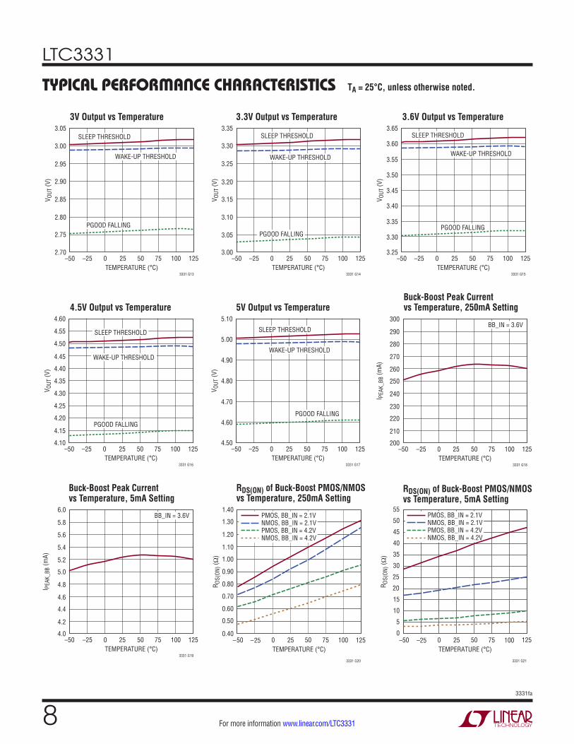
TYPICAL PERFORMANCE CHARACTERISTICS
3V Output vs Temperature 3.3V Output vs Temperature 3.6V Output vs Temperature
4.5V Output vs Temperature 5V Output vs Temperature
RDS(ON) of Buck-Boost PMOS/NMOS vs Temperature, 250mA Setting
TEMPERATURE (°C)–50
V OUT
(V)
3.05
3.00
2.95
2.90
2.85
2.80
2.75
2.700 25 50 75 100
3331 G13
125–25
SLEEP THRESHOLD
PGOOD FALLING
WAKE-UP THRESHOLD
TEMPERATURE (°C)–50
V OUT
(V)
3.35
3.30
3.25
3.20
3.15
3.10
3.05
3.000 25 50 75 100
3331 G14
125–25
SLEEP THRESHOLD
PGOOD FALLING
WAKE-UP THRESHOLD
TEMPERATURE (°C)–50
V OUT
(V)
3.65
3.60
3.55
3.50
3.45
3.40
3.35
3.30
3.250 25 50 75 100
3331 G15
125–25
SLEEP THRESHOLD
PGOOD FALLING
WAKE-UP THRESHOLD
TEMPERATURE (°C)–50
V OUT
(V)
4.60
4.55
4.50
4.45
4.40
4.35
4.30
4.25
4.20
4.15
4.100 25 50 75 100
3331 G16
125–25
SLEEP THRESHOLD
PGOOD FALLING
WAKE-UP THRESHOLD
TEMPERATURE (°C)–50
V OUT
(V)
5.10
5.00
4.90
4.80
4.70
4.60
4.500 25 50 75 100
3331 G17
125–25
SLEEP THRESHOLD
PGOOD FALLING
WAKE-UP THRESHOLD
TA = 25°C, unless otherwise noted.
RDS(ON) of Buck-Boost PMOS/NMOS vs Temperature, 5mA Setting
Buck-Boost Peak Current vs Temperature, 250mA Setting
Buck-Boost Peak Current vs Temperature, 5mA Setting
TEMPERATURE (°C)–50
I PEA
K_BB
(mA)
6.0
5.8
5.6
5.4
5.2
4.6
4.4
4.2
5.0
4.0
4.8
0 25 50 75 100
3331 G19
125–25
BB_IN = 3.6V
TEMPERATURE (°C)–50
I PEA
K_BB
(mA)
300
290
280
270
260
230
220
210
250
200
240
0 25 50 75 100
3331 G18
125–25
BB_IN = 3.6V
TEMPERATURE (°C)–50
0.40
R DS(
ON) (
Ω)
0.50
0.70
0.80
0.90
1.40
1.10
0 50 75 100
3331 G20
0.60
1.20
1.30
1.00
–25 25 125
PMOS, BB_IN = 2.1VNMOS, BB_IN = 2.1VPMOS, BB_IN = 4.2VNMOS, BB_IN = 4.2V
TEMPERATURE (°C)–50
R DS(
ON) (
Ω)
15
45
50
55
0 50 75
3331 G21
5
35
25
10
40
0
30
20
–25 25 100 125
PMOS, BB_IN = 2.1VNMOS, BB_IN = 2.1VPMOS, BB_IN = 4.2VNMOS, BB_IN = 4.2V
LTC3331
93331fa
For more information www.linear.com/LTC3331
TYPICAL PERFORMANCE CHARACTERISTICS
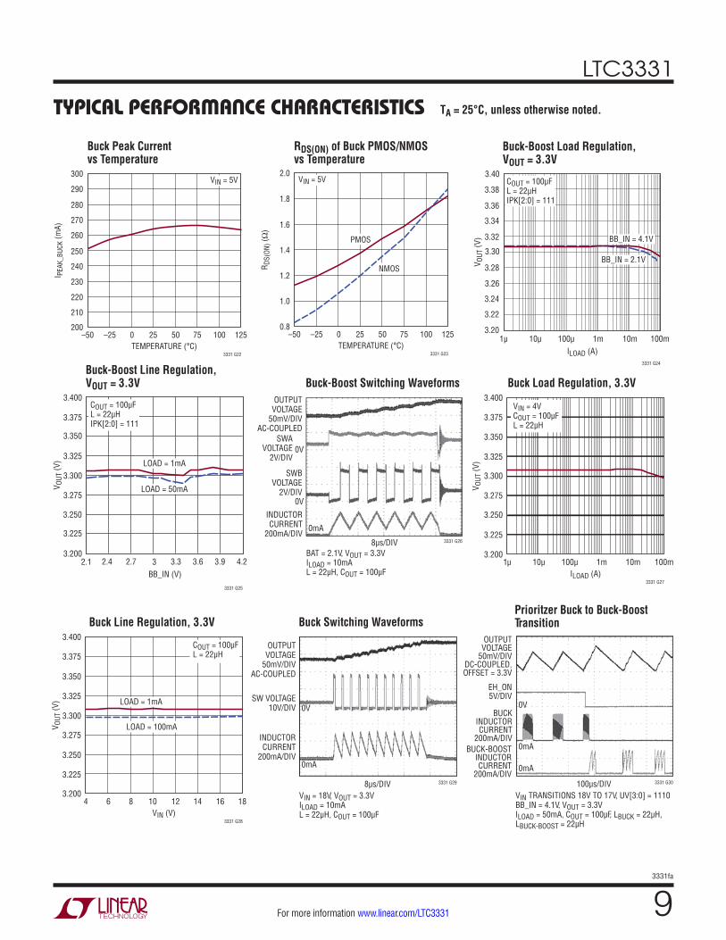
Buck-Boost Load Regulation, VOUT = 3.3V
Buck-Boost Line Regulation, VOUT = 3.3V Buck-Boost Switching Waveforms Buck Load Regulation, 3.3V
TA = 25°C, unless otherwise noted.
ILOAD (A)
V OUT
(V)
3.400
3.375
3.350
3.325
3.300
3.275
3.225
3.250
3.200
3331 G27
1µ 10µ 10m 100m1m100µ
VIN = 4VCOUT = 100µFL = 22µH
Buck Peak Current vs Temperature
RDS(ON) of Buck PMOS/NMOS vs Temperature
TEMPERATURE (°C)–50
I PEA
K_BU
CK (m
A)
300
290
280
270
260
250
240
230
220
200
210
0 25 50 75 100
3331 G22
125–25
VIN = 5V
TEMPERATURE (°C)–50
R DS(
ON) (
Ω)
2.0
1.8
1.6
1.4
1.2
0.8
1.0
0 25 50 75 100
3331 G23
125–25
VIN = 5V
PMOS
NMOS
ILOAD (A)1µ 10µ
3.28V OUT
(V)
3.30
3.32
3.34
3.36
100µ 1m 10m 100m
3331 G24
3.26
3.24
3.22
3.20
3.38
3.40
BB_IN = 4.1V
BB_IN = 2.1V
COUT = 100µFL = 22µHIPK[2:0] = 111
BB_IN (V)2.1
V OUT
(V)
3.375
3
3331 G25
3.300
3.250
2.4 2.7 3.3
3.225
3.200
3.400
LOAD = 1mA
LOAD = 50mA
COUT = 100µFL = 22µHIPK[2:0] = 111
3.350
3.325
3.275
3.6 3.9 4.2BAT = 2.1V, VOUT = 3.3VILOAD = 10mAL = 22µH, COUT = 100µF
SWAVOLTAGE
2V/DIV
SWBVOLTAGE
2V/DIV
OUTPUTVOLTAGE
50mV/DIVAC-COUPLED
INDUCTORCURRENT
200mA/DIV3331 G268µs/DIV
0V
0V
0mA
Prioritzer Buck to Buck-Boost Transition
VIN TRANSITIONS 18V TO 17V, UV[3:0] = 1110BB_IN = 4.1V, VOUT = 3.3VILOAD = 50mA, COUT = 100µF, LBUCK = 22µH,LBUCK-BOOST = 22µH
0V
0mA
EH_ON5V/DIV
BUCKINDUCTORCURRENT
200mA/DIV
OUTPUTVOLTAGE
50mV/DIVDC-COUPLED,OFFSET = 3.3V
BUCK-BOOSTINDUCTORCURRENT
200mA/DIV0mA
3331 G30100µs/DIV
Buck Line Regulation, 3.3V Buck Switching Waveforms
VIN (V)4
V OUT
(V)
3.400
3.375
3.350
3.325
3.300
3.275
3.250
3.225
3.2008 10 12 14 16
3331 G28
186
LOAD = 1mA
LOAD = 100mA
COUT = 100µFL = 22µH
VIN = 18V, VOUT = 3.3VILOAD = 10mAL = 22µH, COUT = 100µF
0VSW VOLTAGE
10V/DIV
OUTPUTVOLTAGE
50mV/DIVAC-COUPLED
INDUCTORCURRENT
200mA/DIV0mA
3331 G298µs/DIV
LTC3331
103331fa
For more information www.linear.com/LTC3331
TYPICAL PERFORMANCE CHARACTERISTICS
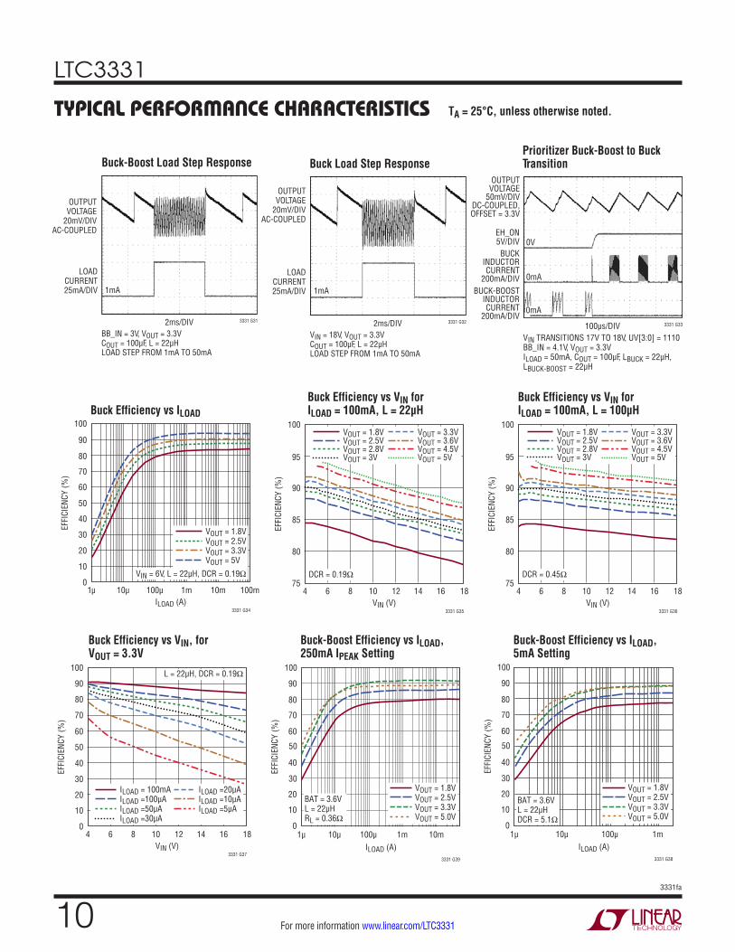
Buck-Boost Load Step Response Buck Load Step ResponsePrioritizer Buck-Boost to Buck Transition
Buck Efficiency vs ILOAD
Buck Efficiency vs VIN for ILOAD = 100mA, L = 22µH
Buck Efficiency vs VIN for ILOAD = 100mA, L = 100µH
TA = 25°C, unless otherwise noted.
BB_IN = 3V, VOUT = 3.3VCOUT = 100µF, L = 22µHLOAD STEP FROM 1mA TO 50mA
OUTPUTVOLTAGE
20mV/DIVAC-COUPLED
LOADCURRENT25mA/DIV 1mA
3331 G312ms/DIVVIN = 18V, VOUT = 3.3VCOUT = 100µF, L = 22µHLOAD STEP FROM 1mA TO 50mA
OUTPUTVOLTAGE
20mV/DIVAC-COUPLED
LOADCURRENT25mA/DIV 1mA
3331 G322ms/DIV
VIN TRANSITIONS 17V TO 18V, UV[3:0] = 1110BB_IN = 4.1V, VOUT = 3.3VILOAD = 50mA, COUT = 100µF, LBUCK = 22µH,LBUCK-BOOST = 22µH
0V
0mA
EH_ON5V/DIVBUCK
INDUCTORCURRENT
200mA/DIV
OUTPUTVOLTAGE
50mV/DIVDC-COUPLED,OFFSET = 3.3V
BUCK-BOOSTINDUCTORCURRENT
200mA/DIV3331 G33100µs/DIV
0mA
ILOAD (A)
EFFI
CIEN
CY (%
)
3331 G34
100
90
60
80
70
40
50
20
10
30
01µ 10µ 10m 100m1m100µ
VOUT = 1.8VVOUT = 2.5VVOUT = 3.3VVOUT = 5V
VIN = 6V, L = 22µH, DCR = 0.19Ω
VIN (V)
EFFI
CIEN
CY (%
)
3331 G35
100
90
95
85
80
754 6 108 12 14 16 18
VOUT = 1.8VVOUT = 2.5VVOUT = 2.8VVOUT = 3V
VOUT = 3.3VVOUT = 3.6VVOUT = 4.5VVOUT = 5V
DCR = 0.19Ω
VIN (V)
EFFI
CIEN
CY (%
)
3331 G36
100
90
95
85
80
754 6 108 12 14 16 18
DCR = 0.45Ω
VOUT = 1.8VVOUT = 2.5VVOUT = 2.8VVOUT = 3V
VOUT = 3.3VVOUT = 3.6VVOUT = 4.5VVOUT = 5V
Buck Efficiency vs VIN, for VOUT = 3.3V
Buck-Boost Efficiency vs ILOAD,5mA Setting
Buck-Boost Efficiency vs ILOAD, 250mA IPEAK Setting
VIN (V)
EFFI
CIEN
CY (%
)
3331 G37
100
80
70
60
90
50
40
30
20
10
04 6 108 12 14 16 18
ILOAD = 100mAILOAD =100µAILOAD =50µAILOAD =30µA
ILOAD =20µAILOAD =10µAILOAD =5µA
L = 22µH, DCR = 0.19Ω
ILOAD (A)1µ
40
EFFI
CIEN
CY (%
)
50
60
70
80
10µ 100µ 1m
3331 G38
30
20
10
0
90
100
VOUT = 1.8VVOUT = 2.5VVOUT = 3.3VVOUT = 5.0V
BAT = 3.6VL = 22µHDCR = 5.1Ω
ILOAD (A)1µ 10µ 100µ
40
EFFI
CIEN
CY (%
)
50
60
70
80
1m 10m
3331 G39
30
20
10
0
90
100
VOUT = 1.8VVOUT = 2.5VVOUT = 3.3VVOUT = 5.0V
BAT = 3.6VL = 22µHRL = 0.36Ω
LTC3331
113331fa
For more information www.linear.com/LTC3331
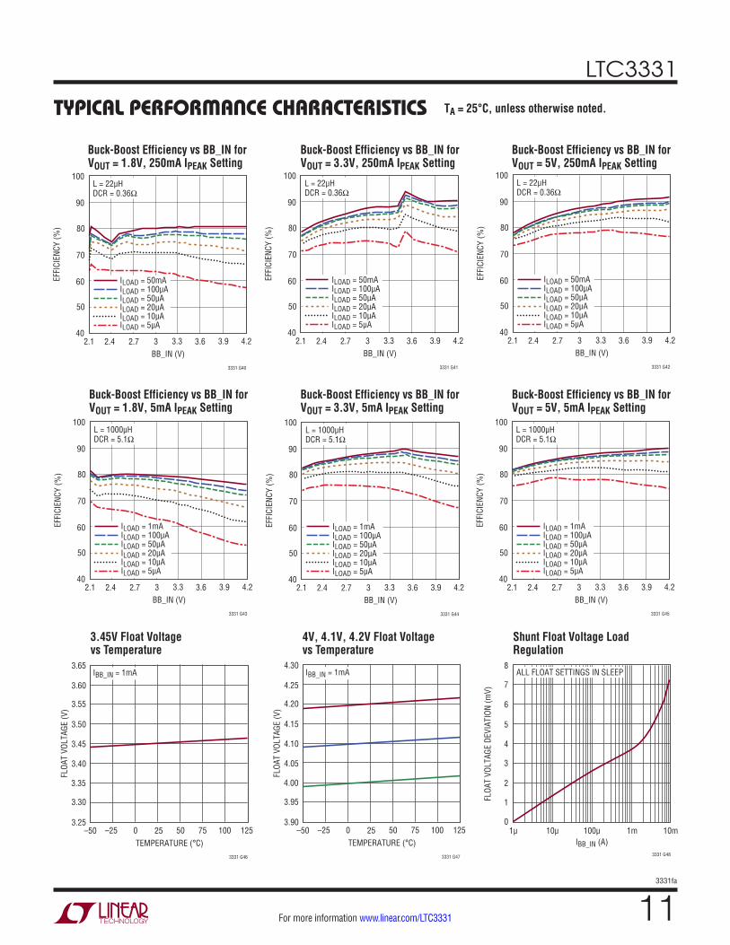
TYPICAL PERFORMANCE CHARACTERISTICS
Buck-Boost Efficiency vs BB_IN for VOUT = 1.8V, 250mA IPEAK Setting
Buck-Boost Efficiency vs BB_IN for VOUT = 3.3V, 250mA IPEAK Setting
Buck-Boost Efficiency vs BB_IN for VOUT = 5V, 250mA IPEAK Setting
Buck-Boost Efficiency vs BB_IN for VOUT = 1.8V, 5mA IPEAK Setting
Buck-Boost Efficiency vs BB_IN for VOUT = 3.3V, 5mA IPEAK Setting
Buck-Boost Efficiency vs BB_IN for VOUT = 5V, 5mA IPEAK Setting
TA = 25°C, unless otherwise noted.
BB_IN (V)2.1
EFFI
CIEN
CY (%
) 80
90
100
3 3.6
3331 G40
70
60
2.4 2.7 3.3 3.9 4.2
50
40
ILOAD = 50mAILOAD = 100µAILOAD = 50µAILOAD = 20µAILOAD = 10µAILOAD = 5µA
L = 22µHDCR = 0.36Ω
BB_IN (V)2.1
EFFI
CIEN
CY (%
) 80
90
100
3 3.6
3331 G41
70
60
2.4 2.7 3.3 3.9 4.2
50
40
ILOAD = 50mAILOAD = 100µAILOAD = 50µAILOAD = 20µAILOAD = 10µAILOAD = 5µA
L = 22µHDCR = 0.36Ω
BB_IN (V)2.1
EFFI
CIEN
CY (%
) 80
90
100
3 3.6
3331 G42
70
60
2.4 2.7 3.3 3.9 4.2
50
40
ILOAD = 50mAILOAD = 100µAILOAD = 50µAILOAD = 20µAILOAD = 10µAILOAD = 5µA
L = 22µHDCR = 0.36Ω
BB_IN (V)2.1
EFFI
CIEN
CY (%
) 80
90
100
3 3.6
3331 G43
70
60
2.4 2.7 3.3 3.9 4.2
50
40
ILOAD = 1mAILOAD = 100µAILOAD = 50µAILOAD = 20µAILOAD = 10µAILOAD = 5µA
L = 1000µHDCR = 5.1Ω
BB_IN (V)2.1
EFFI
CIEN
CY (%
) 80
90
100
3 3.6
3331 G44
70
60
2.4 2.7 3.3 3.9 4.2
50
40
ILOAD = 1mAILOAD = 100µAILOAD = 50µAILOAD = 20µAILOAD = 10µAILOAD = 5µA
L = 1000µHDCR = 5.1Ω
BB_IN (V)2.1
EFFI
CIEN
CY (%
) 80
90
100
3 3.6
3331 G45
70
60
2.4 2.7 3.3 3.9 4.2
50
40
ILOAD = 1mAILOAD = 100µAILOAD = 50µAILOAD = 20µAILOAD = 10µAILOAD = 5µA
L = 1000µHDCR = 5.1Ω
Shunt Float Voltage Load Regulation
4V, 4.1V, 4.2V Float Voltage vs Temperature
3.45V Float Voltage vs Temperature
TEMPERATURE (°C)–50
FLOA
T VO
LTAG
E (V
)
3.60
25
3331 G46
3.45
3.35
–25 0 50
3.30
3.25
3.65IBB_IN = 1mA
3.55
3.50
3.40
75 100 125TEMPERATURE (°C)
–50
FLOA
T VO
LTAG
E (V
)
4.25
25
3331 G47
4.10
4.00
–25 0 50
3.95
3.90
4.30IBB_IN = 1mA
4.20
4.15
4.05
75 100 125IBB_IN (A)
2
FLOA
T VO
LTAG
E DE
VIAT
ION
(mV)
4
5
7
8
1µ 100µ 1m 10m
3331 G48
010µ
6
3
1
ALL FLOAT SETTINGS IN SLEEP
LTC3331
123331fa
For more information www.linear.com/LTC3331
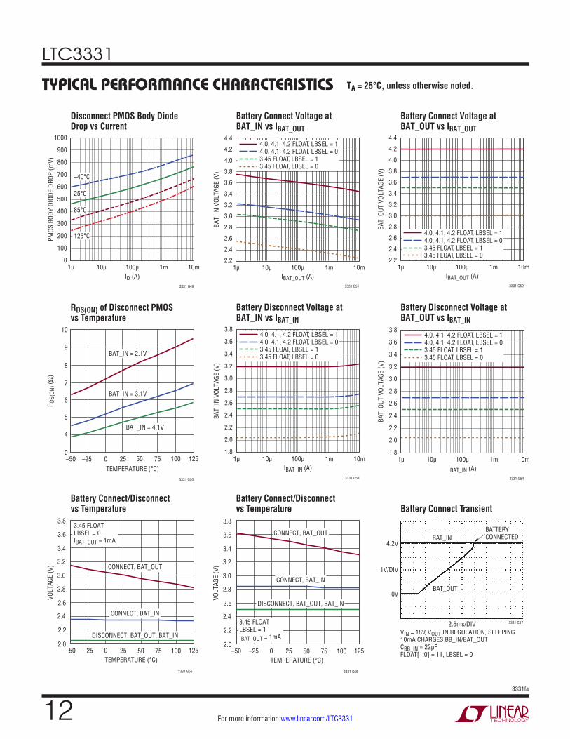
RDS(ON) of Disconnect PMOS vs Temperature
Battery Connect Voltage at BAT_IN vs IBAT_OUT
Battery Disconnect Voltage at BAT_IN vs IBAT_IN
Battery Connect Voltage at BAT_OUT vs IBAT_OUT
Battery Disconnect Voltage at BAT_OUT vs IBAT_IN
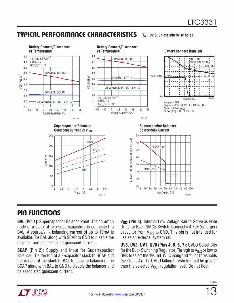
Battery Connect TransientBattery Connect/Disconnect vs Temperature
Battery Connect/Disconnect vs Temperature
TYPICAL PERFORMANCE CHARACTERISTICS TA = 25°C, unless otherwise noted.
Disconnect PMOS Body Diode Drop vs Current
ID (A)
300
PMOS
BOD
Y DI
ODE
DROP
(mV)
900
1000
200
100
800
500
700
600
400
1µ 100µ 1m 10m
3331 G49
010µ
–40°C
125°C
25°C
85°C
TEMPERATURE (°C)–50
7
8
10
25 75
3331 G50
6
5
–25 0 50 100 125
4
0
9
R DS(
ON) (
Ω)
BAT_IN = 2.1V
BAT_IN = 3.1V
BAT_IN = 4.1V
IBAT_OUT (A)
2.6
BAT_
IN V
OLTA
GE (V
)3.0
3.6
4.0
2.4
2.8
3.2
3.4
3.8
1µ 100µ 1m 10m
3331 G51
2.210µ
4.4
4.24.0, 4.1, 4.2 FLOAT, LBSEL = 14.0, 4.1, 4.2 FLOAT, LBSEL = 03.45 FLOAT, LBSEL = 13.45 FLOAT, LBSEL = 0
IBAT_OUT (A)
2.6
BAT_
OUT
VOLT
AGE
(V)
3.0
3.6
4.0
2.4
2.8
3.2
3.4
3.8
1µ 100µ 1m 10m
3331 G52
2.210µ
4.4
4.2
4.0, 4.1, 4.2 FLOAT, LBSEL = 14.0, 4.1, 4.2 FLOAT, LBSEL = 03.45 FLOAT, LBSEL = 13.45 FLOAT, LBSEL = 0
IBAT_IN (A)
2.4BAT_
IN V
OLTA
GE (V
)
3.6
3.8
2.2
2.0
3.4
2.8
3.2
3.0
2.6
1µ 100µ 1m 10m
3331 G53
1.810µ
4.0, 4.1, 4.2 FLOAT, LBSEL = 14.0, 4.1, 4.2 FLOAT, LBSEL = 03.45 FLOAT, LBSEL = 13.45 FLOAT, LBSEL = 0
IBAT_IN (A)
2.4
BAT_
OUT
VOLT
AGE
(V)
3.6
3.8
2.2
2.0
3.4
2.8
3.2
3.0
2.6
1µ 100µ 1m 10m
3331 G54
1.810µ
4.0, 4.1, 4.2 FLOAT, LBSEL = 14.0, 4.1, 4.2 FLOAT, LBSEL = 03.45 FLOAT, LBSEL = 13.45 FLOAT, LBSEL = 0
TEMPERATURE (°C)–50
2.0
VOLT
AGE
(V)
2.2
2.6
2.8
3.0
50
3.8
3331 G55
2.4
0–25 75 10025 125
3.2
3.4
3.6
CONNECT, BAT_OUT
CONNECT, BAT_IN
DISCONNECT, BAT_OUT, BAT_IN
3.45 FLOATLBSEL = 0IBAT_OUT = 1mA
TEMPERATURE (°C)–50
2.0
VOLT
AGE
(V)
2.2
2.6
2.8
3.0
50
3.8
3331 G56
2.4
0–25 75 10025 125
3.2
3.4
3.6 CONNECT, BAT_OUT
CONNECT, BAT_IN
DISCONNECT, BAT_OUT, BAT_IN
3.45 FLOATLBSEL = 1IBAT_OUT = 1mA
2.5ms/DIV 3331 G57
VIN = 18V, VOUT IN REGULATION, SLEEPING10mA CHARGES BB_IN/BAT_OUTCBB_IN = 22µFFLOAT[1:0] = 11, LBSEL = 0
1V/DIV
BAT_OUT
BAT_IN4.2V
0V
BATTERYCONNECTED
LTC3331
133331fa
For more information www.linear.com/LTC3331
Supercapacitor Balancer Quiescent Current vs VSCAP
Supercapacitor Balancer Source/Sink Current
Battery Connect TransientBattery Connect/Disconnect vs Temperature
Battery Connect/Disconnect vs Temperature
TYPICAL PERFORMANCE CHARACTERISTICS TA = 25°C, unless otherwise noted.
TEMPERATURE (°C)–50
2.6
VOLT
AGE
(V)
2.8
3.2
3.4
3.6
50
4.4
3331 G58
3.0
0–25 75 10025 125
3.8
4.0
4.2
CONNECT, BAT_OUT
CONNECT, BAT_IN
DISCONNECT, BAT_OUT, BAT_IN
4.0, 4.1, 4.2 FLOATLBSEL = 0IBAT_OUT = 1mA
TEMPERATURE (°C)–50
2.6
VOLT
AGE
(V)
2.8
3.2
3.4
3.6
50
4.4
3331 G59
3.0
0–25 75 10025 125
3.8
4.0
4.2CONNECT, BAT_OUT
CONNECT, BAT_IN
DISCONNECT, BAT_OUT, BAT_IN
4.0, 4.1, 4.2 FLOATLBSEL = 1IBAT_OUT = 1mA
500ms/DIV 3331 G60
CBAT_IN = 1mFCBB_IN = 22µF, BB_IN TIED TO BAT_OUT1mA LOAD AT VOUTFLOAT[1:0] = 11, LBSEL = 0
500mV/DIV BAT_OUT
BAT_IN
VOUT
0V
BATTERYDISCONNECTED
VSCAP (V)2
I SCA
P (n
A)
250
200
150
100
50
03 4 4.5 53.5
3330 G61
5.52.5
85°C
125°C
25°C
–40°C
VBAL/VSCAP (%)0
BALA
NCER
SOU
RCE/
SINK
CUR
RENT
(mA)
50
40
30
20
10
0
–10
–2020 30 50 60 70 80 9040
3330 G62
10010
SCAP = 5V
SCAP = 2.5V
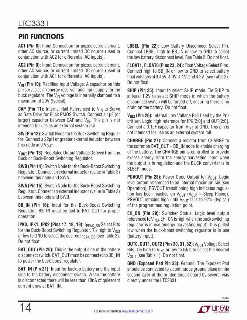
PIN FUNCTIONSBAL (Pin 1): Supercapacitor Balance Point. The common node of a stack of two supercapacitors is connected to BAL. A source/sink balancing current of up to 10mA is available. Tie BAL along with SCAP to GND to disable the balancer and its associated quiescent current.
SCAP (Pin 2): Supply and Input for Supercapacitor Balancer. Tie the top of a 2-capacitor stack to SCAP and the middle of the stack to BAL to activate balancing. Tie SCAP along with BAL to GND to disable the balancer and its associated quiescent current.
VIN2 (Pin 3): Internal Low Voltage Rail to Serve as Gate Drive for Buck NMOS Switch. Connect a 4.7µF (or larger) capacitor from VIN2 to GND. This pin is not intended for use as an external system rail.
UV3, UV2, UV1, UV0 (Pins 4, 5, 6, 7): UVLO Select Bits for the Buck Switching Regulator. Tie high to VIN2 or low to GND to select the desired UVLO rising and falling thresholds (see Table 4). The UVLO falling threshold must be greater than the selected VOUT regulation level. Do not float.
LTC3331
143331fa
For more information www.linear.com/LTC3331
AC1 (Pin 8): Input Connection for piezoelectric element, other AC source, or current limited DC source (used in conjunction with AC2 for differential AC inputs).
AC2 (Pin 9): Input Connection for piezoelectric element, other AC source, or current limited DC source (used in conjunction with AC1 for differential AC inputs).
VIN (Pin 10): Rectified Input Voltage. A capacitor on this pin serves as an energy reservoir and input supply for the buck regulator. The VIN voltage is internally clamped to a maximum of 20V (typical).
CAP (Pin 11): Internal Rail Referenced to VIN to Serve as Gate Drive for Buck PMOS Switch. Connect a 1μF (or larger) capacitor between CAP and VIN. This pin is not intended for use as an external system rail.
SW (Pin 12): Switch Node for the Buck Switching Regula-tor. Connect a 22µH or greater external inductor between this node and VOUT.
VOUT (Pin 13): Regulated Output Voltage Derived from the Buck or Buck-Boost Switching Regulator.
SWB (Pin 14): Switch Node for the Buck-Boost Switching Regulator. Connect an external inductor (value in Table 3) between this node and SWA.
SWA (Pin 15): Switch Node for the Buck-Boost Switching Regulator. Connect an external inductor (value in Table 3)between this node and SWB.
BB_IN (Pin 16): Input for the Buck-Boost Switching Regulator. BB_IN must be tied to BAT_OUT for proper operation.
IPK0, IPK1, IPK2 (Pins 17, 18, 19): IPEAK_BB Select Bits for the Buck-Boost Switching Regulator. Tie high to VIN3 or low to GND to select the desired IPEAK_BB (see Table 3). Do not float.
BAT_OUT (Pin 20): This is the output side of the battery disconnect switch. BAT_OUT must be connected to BB_IN to power the buck-boost regulator.
BAT_IN (Pin 21): Input for backup battery and the input side to the battery disconnect switch. When the battery is disconnected there will be less than 10nA of quiescent current draw at BAT_IN.
PIN FUNCTIONSLBSEL (Pin 22): Low Battery Disconnect Select Pin. Connect LBSEL high to BB_IN or low to GND to select the low battery disconnect level. See Table 2. Do not float.
FLOAT1, FLOAT0 (Pins 23, 24): Float Voltage Select Pins. Connect high to BB_IN or low to GND to select battery float voltages of 3.45V, 4.0V, 4.1V, and 4.2V (see Table 2). Do not float.
SHIP (Pin 25): Input to select SHIP mode. Tie SHIP to at least 1.2V to select SHIP mode in which the battery disconnect switch will be forced off, ensuring there is no drain on the battery. Do not float.
VIN3 (Pin 26): Internal Low Voltage Rail Used by the Pri-oritizer. Logic high reference for IPK[2:0] and OUT[2:0].Connect a 0.1µF capacitor from VIN3 to GND. This pin is not intended for use as an external system rail.
CHARGE (Pin 27): Connect a resistor from CHARGE to the common BAT_OUT = BB_IN node to enable charging of the battery. The CHARGE pin is controlled to provide excess energy from the energy harvesting input when the output is in regulation and the BUCK converter is in SLEEP mode.
PGVOUT (Pin 28): Power Good Output for VOUT. Logic level output referenced to an internal maximum rail (see Operation). PGVOUT transitioning high indicates regula-tion has been reached on VOUT (VOUT = Sleep Rising). PGVOUT remains high until VOUT falls to 92% (typical) of the programmed regulation point.
EH_ON (Pin 29): Switcher Status. Logic level output referenced to VIN3. EH_ON is high when the buck switching regulator is in use (energy harvesting input). It is pulled low when the buck-boost switching regulator is in use (battery input).
OUT0, OUT1, OUT2 (Pins 30, 31, 32): VOUT Voltage Select Bits. Tie high to VIN3 or low to GND to select the desired VOUT (see Table 1). Do not float.
GND (Exposed Pad Pin 33): Ground. The Exposed Pad should be connected to a continuous ground plane on the second layer of the printed circuit board by several vias directly under the LTC3331.
LTC3331
153331fa
For more information www.linear.com/LTC3331
BLOCK DIAGRAM
3331 BD
BANDGAPREFERENCE
INTERNALRAIL
GENERATION
PRIORITZER
UVLO
UVLO_SET
SLEEP
VIN
VREF
AC1
20V
10
8
AC2
BB_IN
9
16
EH_ON
SLEEP
ILIM_SET
VREFVIN2
VIN2
VIN3
BB_IN VOUT
BAT_OUT
CHARGE
SLEEP-UVLO
BAT_IN
SHIP LBSEL
BODYDIODE
SHUNTPMOS
29
27
20
21
+
–
–
+
VREF
0.925*VREF
SLEEP–
+
–
+ VREF
VIN2 VIN3VIN3
CAP11
SW
VIN2
GND33
SWA
SWB
VOUT
15
14
13
PGVOUT
SCAP
BAL
28
2
1
VIN326
BUCK-BOOSTCONTROL
ILIM_SETUVLO_SET
12
3
4 3
4, 5, 6, 7 19, 18, 17
3
32, 31, 3023, 24OUT[2:0]FLOAT[1:0] UV[3:0] IPK[2:0]
BUCKCONTROL
–
+
BB_INBB_IN
2
25 22
EA
LTC3331
163331fa
For more information www.linear.com/LTC3331
OPERATIONModes of Operation
The following four tables detail all programmable settings on the LTC3331.Table 1. Output Voltage Selection
OUT2 OUT1 OUT0 VOUT
0 0 0 1.8V
0 0 1 2.5V
0 1 0 2.8V
0 1 1 3.0V
1 0 0 3.3V
1 0 1 3.6V
1 1 0 4.5V
1 1 1 5.0V
Table 2. FLOAT SelectionLBSEL FLOAT1 FLOAT0 FLOAT CONNECT DISCONNECT
0 0 0 3.45V 2.35 2.04
0 0 1 4.0V 3.03 2.70
0 1 0 4.1V 3.03 2.70
0 1 1 4.2V 3.03 2.70
1 0 0 3.45V 2.85 2.51
1 0 1 4.0V 3.53 3.20
1 1 0 4.1V 3.53 3.20
1 1 1 4.2V 3.53 3.20
Table 3. IPEAK_BB SelectionIPK2 IPK1 IPK0 ILIM LMIN
0 0 0 5mA 1000µH
0 0 1 10mA 470µH
0 1 0 15mA 330µH
0 1 1 25mA 220µH
1 0 0 50mA 100µH
1 0 1 100mA 47µH
1 1 0 150mA 33µH
1 1 1 250mA 22µH
Table 4.UVLO Selection
UV3 UV2 UV1 UV0UVLO
RISINGUVLO
FALLING
0 0 0 0 4V 3V
0 0 0 1 5V 4V
0 0 1 0 6V 5V
0 0 1 1 7V 6V
0 1 0 0 8V 7V
0 1 0 1 8V 5V
0 1 1 0 10V 9V
0 1 1 1 10V 5V
1 0 0 0 12V 11V
1 0 0 1 12V 5V
1 0 1 0 14V 13V
1 0 1 1 14V 5V
1 1 0 0 16V 15V
1 1 0 1 16V 5V
1 1 1 0 18V 17V
1 1 1 1 18V 5V
LTC3331
173331fa
For more information www.linear.com/LTC3331
Overview
The LTC3331 combines a buck switching regulator and a buck-boost switching regulator to produce an energy harvesting solution with battery backup. The converters are controlled by a prioritizer that selects which converter to use based on the availability of a battery and/or har-vestable energy. If harvested energy is available the buck regulator is active and the buck-boost is OFF. An onboard 10mA shunt battery charger with low battery disconnect enables charging of the backup battery to greatly extend the life of the battery. An optional supercapacitor balancer allows for significant energy storage at the output to handle a variety of load requirements.
Energy Harvester
The energy harvester is an ultralow quiescent current power supply designed to interface directly to a piezoelectric or alternative A/C power source, rectify the input voltage, and store harvested energy on an external capacitor while maintaining a regulated output voltage. It can also bleed off any excess input power via an internal protective shunt regulator. It consists of an internal bridge rectifier, an un-dervoltage lockout circuit, and a synchronous buck DC/DC.
Internal Bridge Rectifier
An internal full-wave bridge rectifier accessible via the dif-ferential AC1 and AC2 inputs rectifies AC sources such as those from a piezoelectric element. The rectified output is stored on a capacitor at the VIN pin and can be used as an energy reservoir for the buck converter. The bridge rectifier has a total drop of about 800mV at typical piezo-generated currents (~10μA), but is capable of carrying up to 50mA. Either side of the bridge can be operated independently as a single-ended AC or DC input.
Buck Undervoltage Lockout (UVLO)
When the voltage on VIN rises above the UVLO rising threshold the buck converter is enabled and charge is transferred from the input capacitor to the output capaci-tor. When the input capacitor voltage is depleted below the UVLO falling threshold the buck converter is disabled. These thresholds can be set according to Table 4 which
OPERATION
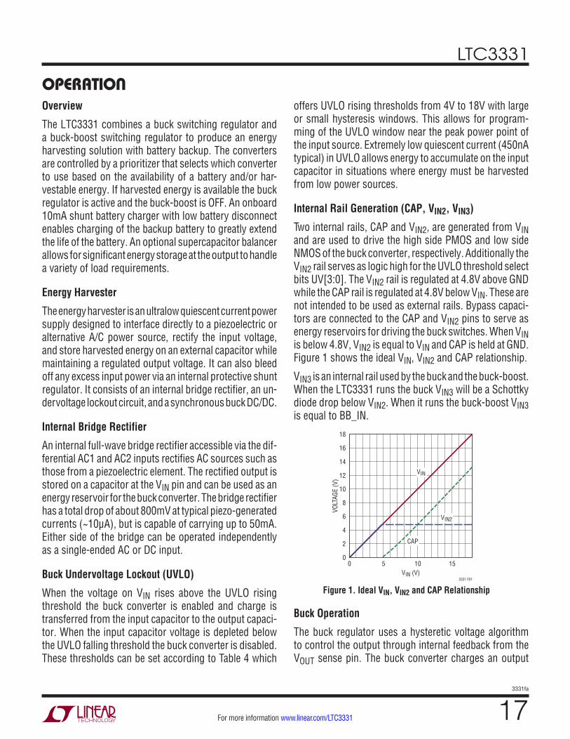
Figure 1. Ideal VIN, VIN2 and CAP Relationship
offers UVLO rising thresholds from 4V to 18V with large or small hysteresis windows. This allows for program-ming of the UVLO window near the peak power point of the input source. Extremely low quiescent current (450nA typical) in UVLO allows energy to accumulate on the input capacitor in situations where energy must be harvested from low power sources.
Internal Rail Generation (CAP, VIN2, VIN3)
Two internal rails, CAP and VIN2, are generated from VIN and are used to drive the high side PMOS and low side NMOS of the buck converter, respectively. Additionally the VIN2 rail serves as logic high for the UVLO threshold select bits UV[3:0]. The VIN2 rail is regulated at 4.8V above GND while the CAP rail is regulated at 4.8V below VIN. These are not intended to be used as external rails. Bypass capaci-tors are connected to the CAP and VIN2 pins to serve as energy reservoirs for driving the buck switches. When VIN is below 4.8V, VIN2 is equal to VIN and CAP is held at GND. Figure 1 shows the ideal VIN, VIN2 and CAP relationship.
VIN3 is an internal rail used by the buck and the buck-boost. When the LTC3331 runs the buck VIN3 will be a Schottky diode drop below VIN2. When it runs the buck-boost VIN3 is equal to BB_IN.
VIN (V)0
VOLT
AGE
(V)
18
12
14
16
10
2
4
8
6
0105
3331 F01
15
VIN
VIN2
CAP
Buck Operation
The buck regulator uses a hysteretic voltage algorithm to control the output through internal feedback from the VOUT sense pin. The buck converter charges an output
LTC3331
183331fa
For more information www.linear.com/LTC3331
OPERATIONcapacitor through an inductor to a value slightly higher than the regulation point. It does this by ramping the inductor current up to IPEAK_BUCK through an internal PMOS switch and then ramping it down to 0mA through an internal NMOS switch. This efficiently delivers energy to the output capacitor. The ramp rate is determined by VIN, VOUT, and the inductor value. When the buck brings the output voltage into regulation the converter enters a low quiescent current sleep state that monitors the out-put voltage with a sleep comparator. During sleep load current is provided by the output capacitor. When the output voltage falls below the regulation point the buck regulator wakes up and the cycle repeats. This hysteretic method of providing a regulated output reduces losses associated with FET switching and maintains the output at light loads. The buck delivers a minimum of 100mA of average load current when it is switching. VOUT can be set from 1.8V to 5V via the output voltage select bits, OUT[2:0] (see Table 1).
When the sleep comparator senses that the output has reached the sleep threshold the buck converter may be in the middle of a cycle with current still flowing through the inductor. Normally both synchronous switches would turn off and the current in the inductor would freewheel to zero through the NMOS body diode. Instead, the NMOS switch is kept on to prevent the conduction loss that would occur in the diode if the NMOS were off. If the PMOS is on when the sleep comparator trips the NMOS will turn on immediately in order to ramp down the current. If the NMOS is on it will be kept on until the current reaches zero.
Though the quiescent current when the buck is switching is much greater than the sleep quiescent current, it is still a small percentage of the average inductor current which results in high efficiency over most load conditions. The buck operates only when sufficient energy has been ac-cumulated in the input capacitor and the length of time the converter needs to transfer energy to the output is much less than the time it takes to accumulate energy. Thus, the buck operating quiescent current is averaged over a long period of time so that the total average quiescent current is low. This feature accommodates sources that harvest small amounts of ambient energy.
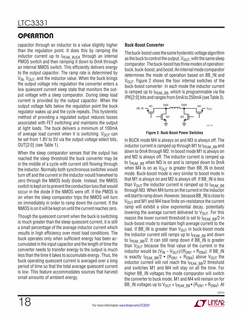
Buck-Boost Converter
The buck-boost uses the same hysteretic voltage algorithm as the buck to control the output, VOUT, with the same sleep comparator. The buck-boost has three modes of operation: buck, buck-boost, and boost. An internal mode comparator determines the mode of operation based on BB_IN and VOUT. Figure 2 shows the four internal switches of the buck-boost converter. In each mode the inductor current is ramped up to IPEAK_BB, which is programmable via the IPK[2:0] bits and ranges from 5mA to 250mA (see Table 3).
In BUCK mode M4 is always on and M3 is always off. The inductor current is ramped up through M1 to IPEAK_BB and down to 0mA through M2. In boost mode M1 is always on and M2 is always off. The inductor current is ramped up to IPEAK_BB when M3 is on and is ramped down to 0mA when M4 is on as VOUT is greater than BB_IN in boost mode. Buck-boost mode is very similar to boost mode in that M1 is always on and M2 is always off. If BB_IN is less than VOUT the inductor current is ramped up to IPEAK_BB through M3. When M4 turns on the current in the inductor will start to ramp down. However, because BB_IN is close to VOUT and M1 and M4 have finite on-resistance the current ramp will exhibit a slow exponential decay, potentially lowering the average current delivered to VOUT. For this reason the lower current threshold is set to IPEAK_BB/2 in buck-boost mode to maintain high average current to the load. If BB_IN is greater than VOUT in buck-boost mode the inductor current still ramps up to IPEAK_BB and down to IPEAK_BB/2. It can still ramp down if BB_IN is greater than VOUT because the final value of the current in the inductor would be (VIN – VOUT)/(RON1 + RON4). If BB_IN is exactly IPEAK_BB/2 • (RON1 + RON4) above VOUT the inductor current will not reach the IPEAK_BB/2 threshold and switches M1 and M4 will stay on all the time. For higher BB_IN voltages the mode comparator will switch the converter to buck mode. M1 and M4 will remain on for BB_IN voltages up to VOUT + IPEAK_BB • (RON1 + RON4). At
Figure 2: Buck-Boost Power Switches
3331 F02
SWA SWBM1BB_IN
M4VOUT
M3M2
LTC3331
193331fa
For more information www.linear.com/LTC3331
this point the current in the inductor is equal to IPEAK_BB and the IPEAK_BB comparator will trip turning off M1 and turning on M2 causing the inductor current to ramp down to IZERO, completing the transition from buck-boost mode to buck mode.
VOUT Power Good
A power good comparator is provided for the VOUT output. It transitions high the first time the LTC3331 goes to sleep, indicating that VOUT has reached regulation. It transitions low when VOUT falls to 92% (typical) of its regulation value. The PGVOUT output is referenced to an internal rail that is generated to be the highest of VIN2, BB_IN, and VOUT less a Schottky diode drop.
Shunt Battery Charger
The LTC3331 provides a reliable low quiescent current shunt battery charger to facilitate charging a battery with harvested energy. A low battery disconnect feature provides protection to the battery from overdischarge by disconnecting the battery from the buck-boost input at a programmable level.
To use the charger connect the battery to the BAT_IN pin. An internal low battery disconnect PMOS switch is connected between the BAT_IN pin and the BAT_OUT pin. The BAT_OUT pin must be connected to BB_IN for proper operation. A charging resistor connected from VIN to BAT_OUT or from CHARGE to BAT_OUT will charge the battery through the body diode of the disconnect PMOS until the battery voltage rises above the low-battery connect threshold. Depending on the capacity of the battery and the input decoupling capacitor, the common BAT_OUT = BB_IN node voltage generally rises or falls to VBAT_IN when the PMOS turns on. Once the PMOS is on the charge current is determined by the charging resistor, the battery voltage, and the voltage of the charging source.
As the battery voltage approaches the float voltage, the LTC3331 shunts current away from the battery thereby reducing the charging current. The LTC3331 can shunt up to 10mA. Float voltages of 3.45V, 4.0V, 4.1V, and 4.2V are programmable via the FLOAT[1:0] pins (see Table 2).
Charging can occur through a resistor connected to VIN or the CHARGE pin. An internal set of back to back PMOS
switches are connected between CHARGE and VIN2 and are turned on only when the energy harvesting buck converter is sleeping. In this way charging of the battery only hap-pens when there is excess harvested energy available and the VOUT output is prioritized over charging of the battery. The charge current available from this pin is limited by the strength of the VIN2 LDO and an appropriate charging resis-tor must be selected to limit this current. The on resistance of the internal charge switches combined is approximately 60Ω. To charge with higher currents connect a resistor directly to VIN. Note that when charging from VIN the bat-tery is always being charged. Care must be taken to ensure that enough power is available to bring up the VOUT output.
Low Battery Disconnect/Connect: LBD/LBC
The low battery disconnect (VLBD) and connect (VLBC) voltage levels are programmed by the LBSEL and FLOAT[1:0] pins (see Table 2). As shown in the Block Diagram the battery disconnects from the common BAT_OUT = BB_IN node by shutting off the PMOS switch when the BAT_IN voltage falls below VLBD. This disconnect function protects Li-Ion batteries from permanent damage due to deep discharge. Disconnecting the battery from the common BAT_OUT = BB_IN node prevents the load as well as the LTC3331 quiescent current from further discharging the battery.
Once disconnected the common BAT_OUT = BB_IN node voltage collapses towards ground. When an input supply is reconnected the battery charges through the internal body diode of the disconnect PMOS. The input supply voltage should be larger than VLBC_BAT_OUT to ensure that the PMOS is turned on. When the voltage reaches VLBC_BAT_OUT, the PMOS turns on and connects the common BAT_OUT = BB_IN node to BAT_IN. While disconnected, the BAT_IN pin voltage is indirectly sensed through the PMOS body diode. Therefore VLBC_BAT_IN varies with charge current and junction temperature. See the Typical Performance Characteristics section for more information.
Low Battery Select
The low battery disconnect voltage level is programmed by the LBSEL pin for each float setting. The LBSEL pin allows the user to trade-off battery run time and maximum shelf life. A lower battery disconnect threshold maximizes run
OPERATION
LTC3331
203331fa
For more information www.linear.com/LTC3331
time by allowing the battery to fully discharge before the disconnect event. Conversely, by increasing the low battery disconnect threshold more capacity remains following the disconnect event which extends the shelf life of the battery. For maximum run time, tie LBSEL to GND. For extended shelf life, tie LBSEL to the common BAT_OUT = BB_IN node. If a high peak current event is expected, users may temporarily select the lower disconnect threshold. This avoids disconnecting the battery too early when the load works against the battery series resistance and temporarily reduces the common BAT_OUT = BB_IN node.
Ship Mode
A ship mode is provided which manually disconnects the battery. This may be useful to prevent discharge of the battery in situations when no harvestable energy is expected for a long period of time such as during shipping. Bring the SHIP pin high to engage ship mode. The low battery disconnect PMOS will turn off, disconnecting the battery at BAT_IN from the common BAT_OUT = BB_IN node. If no harvestable energy is present to hold up the common BAT_OUT = BB_IN node that voltage will collapse. Typically an additional 1µA of quiescent current will appear on BB_IN while SHIP mode is engaged.
To exit SHIP mode first bring the SHIP pin low. If the BB_IN voltage had collapsed while in SHIP mode it must now be brought above the LBC threshold to reconnect the battery. This can be done manually or from an energy harvesting charging source. If harvestable energy had been propping up the common BAT_OUT = BB_IN node voltage above the LBC threshold then the battery will be connected immediately.
Prioritizer
The input prioritizer on the LTC3331 decides whether to use the energy harvesting input or the battery input to power VOUT. If a battery is powering the buck-boost converter and harvested energy causes a UVLO rising transition on VIN, the prioritizer will shut off the buck-boost and turn on the buck, orchestrating a smooth transition that maintains regulation of VOUT.
OPERATIONWhen harvestable energy disappears, the prioritizer will first poll the BB_IN voltage. If the BB_IN voltage is above 1.8V the prioritizer will switch back to the buck-boost while maintaining regulation. If the BB_IN voltage is below 1.8V the buck-boost is not enabled and VOUT cannot be supported until harvestable energy is again available. If the battery is connected then the BB_IN voltage will be above 1.8V for every float and LBSEL combination. If the battery is disconnected the BB_IN voltage will have collapsed below 1.8V and the prioritizer will not switch to the buck-boost when harvestable energy goes away. In the event that the battery is depleted and is disconnected while powering the buck-boost the prioritizer will not switch back to VIN until harvested energy is again available.
If either BB_IN or VIN is grounded, the prioritizer allows the other input to run if its input is high enough for op-eration. The specified quiescent current in UVLO is valid upon start-up of the VIN input and when the battery has taken over regulation of the output. If the battery is less than 1.8V when UVLO is entered and the prioritizer does not enable the buck-boost several hundred nanoamperes of additional quiescent current will appear on VIN.
When the prioritizer selects the VIN input the current on the BB_IN input drops to 200nA. However, if the voltage on BB_IN is higher than VIN2, a fraction of the VIN quiescent current will appear on BB_IN due to internal level shifting. This only affects a small range of battery voltages and UVLO settings.
A digital output, EH_ON, is low when the prioritizer has selected the BB_IN input and is high when the prioritizer has selected the VIN input. The EH_ON output is referenced to VIN3.
Supercapacitor Balancer
An integrated supercapacitor balancer with 150nA of quiescent current is available to balance a stack of two supercapacitors. Typically the input, SCAP, will tie to VOUT to allow for increased energy storage at VOUT with supercapacitors. The BAL pin is tied to the middle of the stack and can source and sink 10mA to regulate the BAL pin’s voltage to half that of the SCAP pin’s voltage. To disable the balancer and its associated quiescent current the SCAP and BAL pins can be tied to ground.
LTC3331
213331fa
For more information www.linear.com/LTC3331
APPLICATIONS INFORMATIONThe LTC3331 allows for energy harvesting from a variety of alternative energy sources in order to power a wireless sensor system and charge a battery. The extremely low quiescent current of the LTC3331 facilitates harvesting from sources generating only microamps of current. The onboard bridge rectifier is suitable for AC piezoelectric or electromagnetic sources as well as providing reverse protection for DC sources such as solar and thermoelec-tric generators. The LTC3331 powers the VOUT output continuously by seamlessly switching between the energy harvesting and battery inputs.
When harvestable energy is available, it is transferred through the bridge rectifier where it accumulates on the VIN capacitor. A low quiescent current UVLO mode allows the voltage on the capacitor to increase towards a programmed UVLO rising threshold. When the voltage rises to this level, the buck converter turns on and transfers energy to VOUT. As energy is transferred the voltage at VIN may decrease to the UVLO falling threshold. If this happens, the buck converter turns off and the buck-boost then turns on to service the load from the battery input while more energy is harvested. When the buck is running the quiescent current on the BB_IN pin drops to the 200nA required by the shunt battery charger.
The LTC3331 is well suited to wireless systems which consume low average power but occasionally need a higher concentrated burst of power to accomplish a task. If these bursts occur with a low duty cycle such that the total energy needed for a burst can be accumulated between bursts then the output can be maintained entirely by the harvester. If the bursts need to happen more frequently or if harvestable energy goes away the battery will be used. If enough energy is available the energy harvester will bring the output up and enter the low quiescent current sleep state and excess energy can be used to charge the battery.
Piezo Energy Harvesting
Ambient vibrational energy can be harvested with a piezoelectric transducer which produces a voltage and current in response to strain. Common piezoelectric elements are PZT (lead zirconate titanate) ceramics, PVDF
(polyvinylidene fluoride) polymers, or other composites. Ceramic piezoelectric elements exhibit a piezoelectric effect when the crystal structure of the ceramic is compressed and internal dipole movement produces a voltage. Polymer elements comprised of long-chain molecules produce a voltage when flexed as molecules repel each other. Ceramics are often used under direct pressure while a polymer is commonly used as a cantilevered beam.
A wide range of piezoelectric elements are available and produce a variety of open-circuit voltages and short-circuit currents. Typically the open-circuit voltage and short-circuit currents increase with available vibrational energy as shown in Figure 3. Piezoelectric elements can be placed in series or in parallel to achieve desired open-circuit voltages.
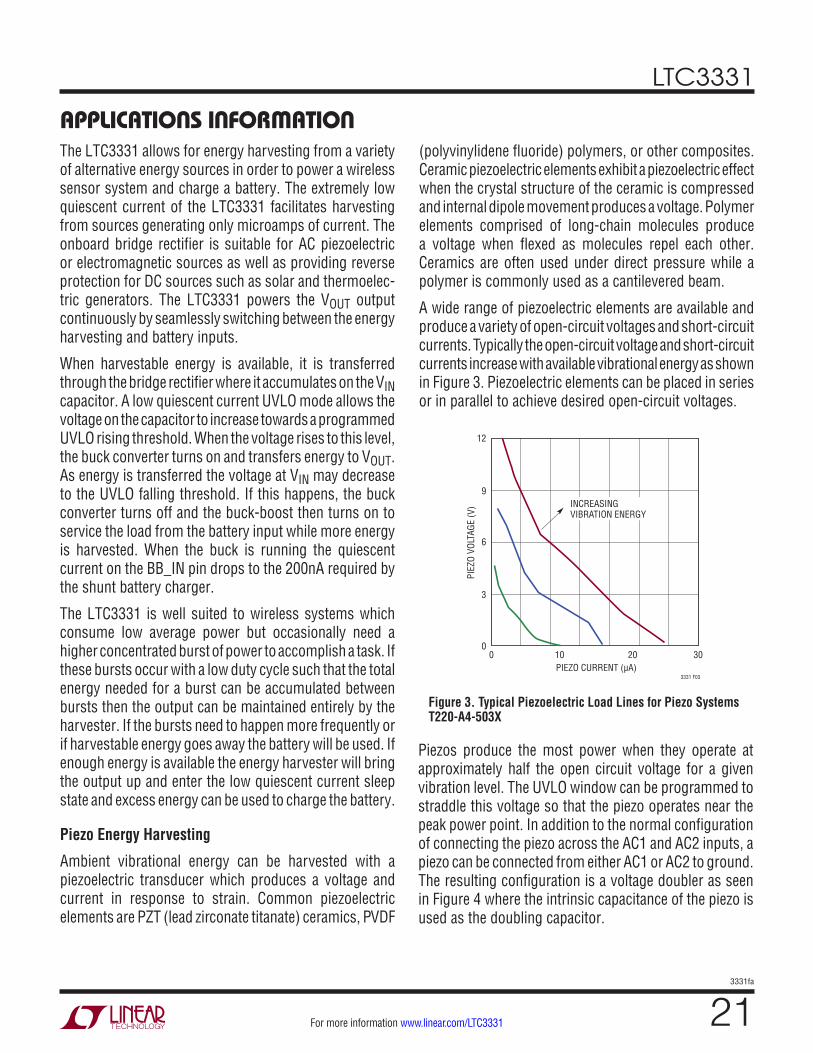
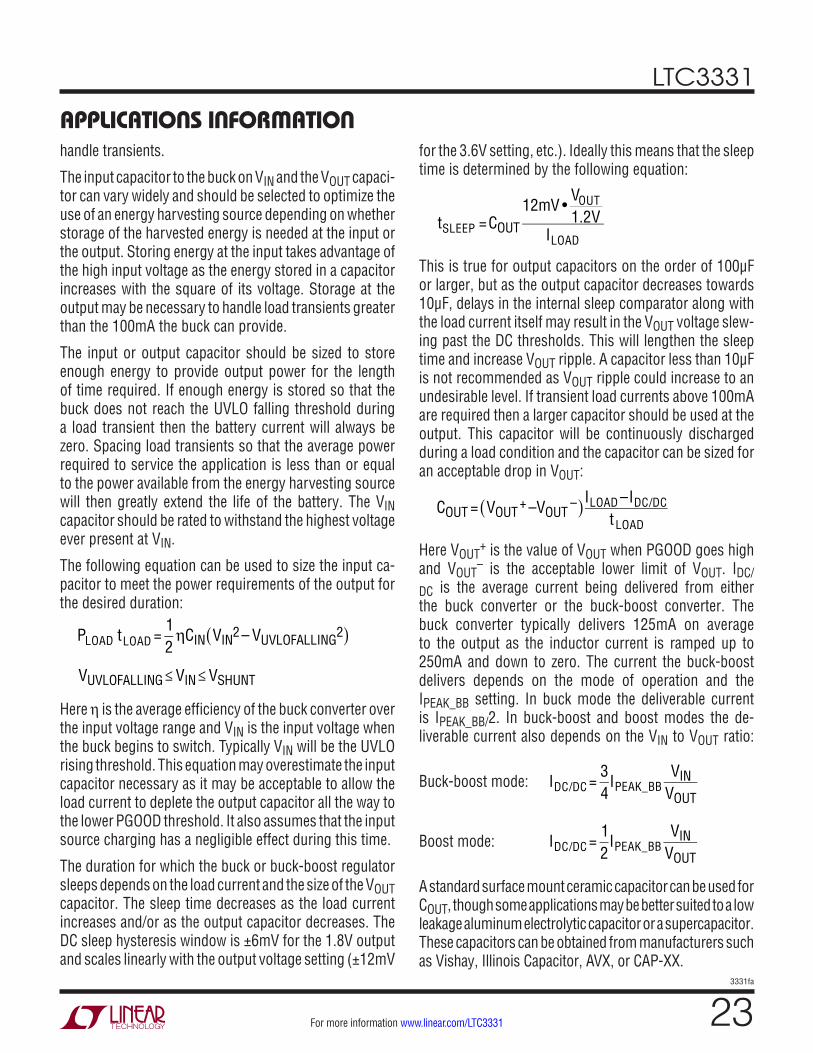
Piezos produce the most power when they operate at approximately half the open circuit voltage for a given vibration level. The UVLO window can be programmed to straddle this voltage so that the piezo operates near the peak power point. In addition to the normal configuration of connecting the piezo across the AC1 and AC2 inputs, a piezo can be connected from either AC1 or AC2 to ground. The resulting configuration is a voltage doubler as seen in Figure 4 where the intrinsic capacitance of the piezo is used as the doubling capacitor.
Figure 3. Typical Piezoelectric Load Lines for Piezo Systems T220-A4-503X
PIEZO CURRENT (µA)0
PIEZ
O VO
LTAG
E (V
)
12
9
6
3
02010
3331 F03
30
INCREASINGVIBRATION ENERGY
LTC3331
223331fa
For more information www.linear.com/LTC3331
A second piezo may be connected from AC2 to ground. This may be of use if the second piezo is mechanically tuned to a different resonant frequency present in the system than the first piezo. To achieve maximum power transfer from the piezo with the doubler the UVLO window should be set to the open circuit voltage of the piezo.
Piezoelectric elements are available from the manufactur-ers listed in Table 5.Table 5. Piezoelectric Element ManufacturersAdvanced Cerametrics www.advancedcerametrics.com
Piezo Systems www.piezo.com
Measurement Specialties www.meas-spec.com
PI (Physik Instrumente) www.pi-usa.us
MIDE Technology Corporation www.mide.com
Morgan Technical Ceramics www.morganelectroceramics.com
Electromagnetic Energy Harvesting
Another alternative AC source is an electromagnetic vibra-tion harvester in which a magnet vibrating inside a coil induces an AC voltage and current in the coil that can then be rectified and harvested by the LTC3331. The vibration could be ambient to the system or it could be caused by an impulse as in a spring loaded switch.
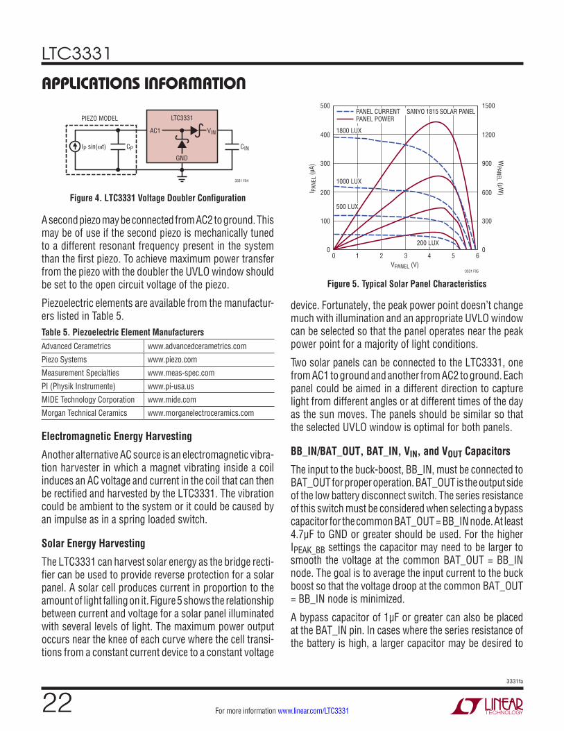
Solar Energy Harvesting
The LTC3331 can harvest solar energy as the bridge recti-fier can be used to provide reverse protection for a solar panel. A solar cell produces current in proportion to the amount of light falling on it. Figure 5 shows the relationship between current and voltage for a solar panel illuminated with several levels of light. The maximum power output occurs near the knee of each curve where the cell transi-tions from a constant current device to a constant voltage
GND
LTC3331PIEZO MODEL
VIN
CIN
AC1
3331 F04
IP sin(ωt) CP
Figure 4. LTC3331 Voltage Doubler Configuration
device. Fortunately, the peak power point doesn’t change much with illumination and an appropriate UVLO window can be selected so that the panel operates near the peak power point for a majority of light conditions.
Two solar panels can be connected to the LTC3331, one from AC1 to ground and another from AC2 to ground. Each panel could be aimed in a different direction to capture light from different angles or at different times of the day as the sun moves. The panels should be similar so that the selected UVLO window is optimal for both panels.
BB_IN/BAT_OUT, BAT_IN, VIN, and VOUT Capacitors
The input to the buck-boost, BB_IN, must be connected to BAT_OUT for proper operation. BAT_OUT is the output side of the low battery disconnect switch. The series resistance of this switch must be considered when selecting a bypass capacitor for the common BAT_OUT = BB_IN node. At least 4.7μF to GND or greater should be used. For the higher IPEAK_BB settings the capacitor may need to be larger to smooth the voltage at the common BAT_OUT = BB_IN node. The goal is to average the input current to the buck boost so that the voltage droop at the common BAT_OUT = BB_IN node is minimized.
A bypass capacitor of 1µF or greater can also be placed at the BAT_IN pin. In cases where the series resistance of the battery is high, a larger capacitor may be desired to
Figure 5. Typical Solar Panel Characteristics
VPANEL (V)0
I PAN
EL (µ
A)
WPANEL (µW
)
500
400
300
200
100
0
1500
1200
900
600
300
02 3 4 5
3331 F05
61
SANYO 1815 SOLAR PANEL
1800 LUX
500 LUX
200 LUX
1000 LUX
PANEL CURRENTPANEL POWER
APPLICATIONS INFORMATION
LTC3331
233331fa
For more information www.linear.com/LTC3331
handle transients.
The input capacitor to the buck on VIN and the VOUT capaci-tor can vary widely and should be selected to optimize the use of an energy harvesting source depending on whether storage of the harvested energy is needed at the input or the output. Storing energy at the input takes advantage of the high input voltage as the energy stored in a capacitor increases with the square of its voltage. Storage at the output may be necessary to handle load transients greater than the 100mA the buck can provide.
The input or output capacitor should be sized to store enough energy to provide output power for the length of time required. If enough energy is stored so that the buck does not reach the UVLO falling threshold during a load transient then the battery current will always be zero. Spacing load transients so that the average power required to service the application is less than or equal to the power available from the energy harvesting source will then greatly extend the life of the battery. The VIN capacitor should be rated to withstand the highest voltage ever present at VIN.
The following equation can be used to size the input ca-pacitor to meet the power requirements of the output for the desired duration:
PLOAD tLOAD =12
ηCIN VIN2 – VUVLOFALLING2( )
VUVLOFALLING≤ VIN≤ VSHUNT
Here η is the average efficiency of the buck converter over the input voltage range and VIN is the input voltage when the buck begins to switch. Typically VIN will be the UVLO rising threshold. This equation may overestimate the input capacitor necessary as it may be acceptable to allow the load current to deplete the output capacitor all the way to the lower PGOOD threshold. It also assumes that the input source charging has a negligible effect during this time.
The duration for which the buck or buck-boost regulator sleeps depends on the load current and the size of the VOUT capacitor. The sleep time decreases as the load current increases and/or as the output capacitor decreases. The DC sleep hysteresis window is ±6mV for the 1.8V output and scales linearly with the output voltage setting (±12mV
for the 3.6V setting, etc.). Ideally this means that the sleep time is determined by the following equation:
tSLEEP =COUT
12mV •VOUT1.2V
ILOAD
This is true for output capacitors on the order of 100μF or larger, but as the output capacitor decreases towards 10μF, delays in the internal sleep comparator along with the load current itself may result in the VOUT voltage slew-ing past the DC thresholds. This will lengthen the sleep time and increase VOUT ripple. A capacitor less than 10μF is not recommended as VOUT ripple could increase to an undesirable level. If transient load currents above 100mA are required then a larger capacitor should be used at the output. This capacitor will be continuously discharged during a load condition and the capacitor can be sized for an acceptable drop in VOUT:
COUT = VOUT
+ –VOUT–( )ILOAD –IDC/DC
tLOAD
Here VOUT+ is the value of VOUT when PGOOD goes high
and VOUT– is the acceptable lower limit of VOUT. IDC/
DC is the average current being delivered from either the buck converter or the buck-boost converter. The buck converter typically delivers 125mA on average to the output as the inductor current is ramped up to 250mA and down to zero. The current the buck-boost delivers depends on the mode of operation and the IPEAK_BB setting. In buck mode the deliverable current is IPEAK_BB/2. In buck-boost and boost modes the de-liverable current also depends on the VIN to VOUT ratio:
Buck-boost mode:
IDC/DC =34
IPEAK_BBVIN
VOUT
Boost mode:
IDC/DC =12
IPEAK_BBVIN
VOUT
A standard surface mount ceramic capacitor can be used for COUT, though some applications may be better suited to a low leakage aluminum electrolytic capacitor or a supercapacitor. These capacitors can be obtained from manufacturers such as Vishay, Illinois Capacitor, AVX, or CAP-XX.
APPLICATIONS INFORMATION
LTC3331
243331fa
For more information www.linear.com/LTC3331
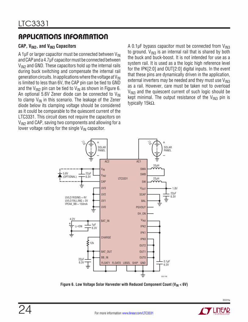
CAP, VIN2, and VIN3 Capacitors
A 1μF or larger capacitor must be connected between VIN and CAP and a 4.7μF capacitor must be connected between VIN2 and GND. These capacitors hold up the internal rails during buck switching and compensate the internal rail generation circuits. In applications where the voltage at VIN is limited to less than 6V, the CAP pin can be tied to GND and the VIN2 pin can be tied to VIN as shown in Figure 6. An optional 5.6V Zener diode can be connected to VIN to clamp VIN in this scenario. The leakage of the Zener diode below its clamping voltage should be considered as it could be comparable to the quiescent current of the LTC3331. This circuit does not require the capacitors on VIN2 and CAP, saving two components and allowing for a lower voltage rating for the single VIN capacitor.
A 0.1µF bypass capacitor must be connected from VIN3 to ground. VIN3 is an internal rail that is shared by both the buck and buck-boost. It is not intended for use as a system rail. It is used as a the logic high reference level for the IPK[2:0] and OUT[2:0] digital inputs. In the event that these pins are dynamically driven in the application, external inverters may be needed and they must use VIN3 as a rail. However, care must be taken not to overload VIN3 and the quiescent current of such logic should be kept minimal. The output resistance of the VIN3 pin is typically 15kΩ.
Figure 6. Low Voltage Solar Harvester with Reduced Component Count (VIN < 6V)
APPLICATIONS INFORMATION
LTC3331
3331 F06
AC1
VIN
CAP
VIN2
AC2
SWA
SWB
VOUT
SW
SCAP
BAL
PGVOUT
EH_ON
VIN3
IPK2
IPK1
IPK0
OUT2
22µH
1.8V
OUT1
OUT00.1µF6.3V
Li-ION
UVLO RISING = 4VUVLO FALLING = 3VIPEAK_BB = 150mA
22µF6.3V
5.6V(OPTIONAL)
UV3
UV2
UV1
UV0
BAT_IN
FLOAT1 FLOAT0 LBSEL SHIP GND
CHARGE
BAT_OUT
BB_IN
+
22µF6.3V
33µH
SOLARPANEL
+
–
SOLARPANEL
+
–
22µF6.3V
1µF6.3V
12k
4.2V
LTC3331
253331fa
For more information www.linear.com/LTC3331
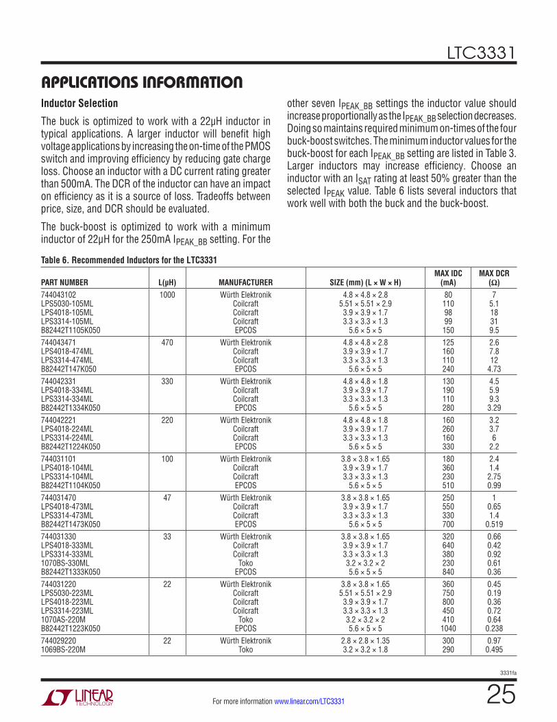
Inductor Selection
The buck is optimized to work with a 22µH inductor in typical applications. A larger inductor will benefit high voltage applications by increasing the on-time of the PMOS switch and improving efficiency by reducing gate charge loss. Choose an inductor with a DC current rating greater than 500mA. The DCR of the inductor can have an impact on efficiency as it is a source of loss. Tradeoffs between price, size, and DCR should be evaluated.
The buck-boost is optimized to work with a minimum inductor of 22μH for the 250mA IPEAK_BB setting. For the
APPLICATIONS INFORMATIONother seven IPEAK_BB settings the inductor value should increase proportionally as the IPEAK_BB selection decreases. Doing so maintains required minimum on-times of the four buck-boost switches. The minimum inductor values for the buck-boost for each IPEAK_BB setting are listed in Table 3. Larger inductors may increase efficiency. Choose an inductor with an ISAT rating at least 50% greater than the selected IPEAK value. Table 6 lists several inductors that work well with both the buck and the buck-boost.
Table 6. Recommended Inductors for the LTC3331
PART NUMBER L(µH) MANUFACTURER SIZE (mm) (L × W × H)MAX IDC
(mA)MAX DCR
(Ω)744043102 LPS5030-105ML LPS4018-105ML LPS3314-105ML B82442T1105K050
1000 Würth Elektronik Coilcraft Coilcraft Coilcraft EPCOS
4.8 × 4.8 × 2.8 5.51 × 5.51 × 2.9 3.9 × 3.9 × 1.7 3.3 × 3.3 × 1.3
5.6 × 5 × 5
80 110 98 99
150
7 5.1 18 31 9.5
744043471 LPS4018-474ML LPS3314-474ML B82442T147K050
470 Würth Elektronik Coilcraft Coilcraft EPCOS
4.8 × 4.8 × 2.8 3.9 × 3.9 × 1.7 3.3 × 3.3 × 1.3
5.6 × 5 × 5
125 160 110 240
2.6 7.8 12
4.73744042331 LPS4018-334ML LPS3314-334ML B82442T1334K050
330 Würth Elektronik Coilcraft Coilcraft EPCOS
4.8 × 4.8 × 1.8 3.9 × 3.9 × 1.7 3.3 × 3.3 × 1.3
5.6 × 5 × 5
130 190 110 280
4.5 5.9 9.3
3.29744042221 LPS4018-224ML LPS3314-224ML B82442T1224K050
220 Würth Elektronik Coilcraft Coilcraft EPCOS
4.8 × 4.8 × 1.8 3.9 × 3.9 × 1.7 3.3 × 3.3 × 1.3
5.6 × 5 × 5
160 260 160 330
3.2 3.7 6
2.2744031101 LPS4018-104ML LPS3314-104ML B82442T1104K050
100 Würth Elektronik Coilcraft Coilcraft EPCOS
3.8 × 3.8 × 1.65 3.9 × 3.9 × 1.7 3.3 × 3.3 × 1.3
5.6 × 5 × 5
180 360 230 510
2.4 1.4
2.75 0.99
744031470 LPS4018-473ML LPS3314-473ML B82442T1473K050
47 Würth Elektronik Coilcraft Coilcraft EPCOS
3.8 × 3.8 × 1.65 3.9 × 3.9 × 1.7 3.3 × 3.3 × 1.3
5.6 × 5 × 5
250 550 330 700
1 0.65 1.4
0.519744031330 LPS4018-333ML LPS3314-333ML 1070BS-330ML B82442T1333K050
33 Würth Elektronik Coilcraft Coilcraft
Toko EPCOS
3.8 × 3.8 × 1.65 3.9 × 3.9 × 1.7 3.3 × 3.3 × 1.3 3.2 × 3.2 × 2 5.6 × 5 × 5
320 640 380 230 840
0.66 0.42 0.92 0.61 0.36
744031220 LPS5030-223ML LPS4018-223ML LPS3314-223ML 1070AS-220M B82442T1223K050
22 Würth Elektronik Coilcraft Coilcraft Coilcraft
Toko EPCOS
3.8 × 3.8 × 1.65 5.51 × 5.51 × 2.9 3.9 × 3.9 × 1.7 3.3 × 3.3 × 1.3 3.2 × 3.2 × 2 5.6 × 5 × 5
360 750 800 450 410
1040
0.45 0.19 0.36 0.72 0.64
0.238744029220 1069BS-220M
22 Würth Elektronik Toko
2.8 × 2.8 × 1.35 3.2 × 3.2 × 1.8
300 290
0.97 0.495
LTC3331
263331fa
For more information www.linear.com/LTC3331
APPLICATIONS INFORMATIONSupercapacitor Balancer
If supercapacitors are used at VOUT the onboard superca-pacitor balancer can be used to balance them with ±10mA of balance current. A list of supercapacitor suppliers is provided in Table 7.Table 7. Supercapacitor ManufacturersCAP-XX www.cap-xx.com
NESS CAP www.nesscap.com
Maxwell www.maxwell.com
Bussman www.cooperbussman.com
AVX www.avx.com
Illinois Capacitor www.illcap.com
Tecate Group www.tecategroup.com
By seamlessly combining a battery source and an en-ergy harvesting source, the LTC3331 enables the use of supercapacitors in energy harvesting applications. The battery provides the initial current required to overcome the effects of the diffusion current when voltage is first applied to the supercapacitors. The energy harvesting source can then support the lower steady state leakage current and average load current.
Summary of Digital inputs and outputs
There are 14 digital pin-strapped logic inputs to the LTC3331 and two digital logic outputs. These and the rails they are referenced to are summarized in Table 8.
Table 8. Digital Pin SummaryINPUT PIN LOGIC HIGH LEVELUV[3:0] VIN2
IPK[2:0] VIN3
OUT[2:0] VIN3
FLOAT[1:0], LBSEL BAT_OUT = BB_INSHIP ≥ 1.2V
OUTPUT PIN LOGIC HIGH LEVELPGVOUT MAX (BB_IN, VIN2, VOUT)EH_ON VIN3
Battery Considerations
The shunt battery charger is designed to work with any single Li-Ion, LiFeP04, or other chemistry with a termination voltage compatible with the available levels. Table 9 lists some batteries, their capacities and their equivalent series resistance (ESR). The ESR causes BAT_OUT and BAT_IN to droop by the product of the load current amplitude multiplied by the ESR. This droop may trigger the low battery disconnect while the battery itself may still have ample capacity. An appropriate bypass capacitor placed at BAT_OUT will help prevent large, low duty cycle load transients from pulling down on BAT_OUT. The bypass capacitor used at BB_IN, which is tied to BAT_OUT, to bypass the buck-boost may be sufficient.
Table 9. Low Capacity Li-Ion and Thin-Film BatteriesMANUFACTURER P/N CAPACITY RESISTANCE VMIN
CYMBET CBC012 12μAh 5k to 10k 3.0V
CYMBET CBC050 50μAh 1500Ω to 3k 3.0V
GM Battery GMB031009 8mAh 10Ω to 20Ω 2.75V
GS NanoTech N/A 500μAh 40Ω 3.0V
Power Stream LIR2032 40mAh 0.6Ω 3.0V
Charging the BatteryCharging the battery with the CHARGE pin allows the battery to be charged only when the energy harvester is sleeping, which prioritizes the VOUT output over the battery. The current that the CHARGE pin can supply is limited to 2mA and an appropriately chosen current limiting resistor should be used. Use the following equation to calculate the value of this resistor:
RCHARGE = 4.8V – VLBD
ICHARGE– 60Ω
Here 4.8V is the output of the VIN2 LDO which is the sup-ply to the CHARGE pin, VLBD is the selected low battery disconnect threshold, 60Ω is the resistance of the CHARGE pin PMOS, and ICHARGE is the desired charge current. For high charging currents approaching 2mA, a larger VIN2 capacitor may improve transient behavior.
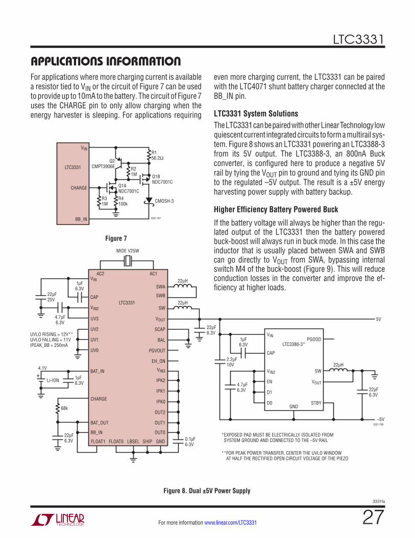
LTC3331
273331fa
For more information www.linear.com/LTC3331
Figure 8. Dual ±5V Power Supply
APPLICATIONS INFORMATIONFor applications where more charging current is available a resistor tied to VIN or the circuit of Figure 7 can be used to provide up to 10mA to the battery. The circuit of Figure 7 uses the CHARGE pin to only allow charging when the energy harvester is sleeping. For applications requiring
Q2CMPT3906E
Q1BNDC7001C
Q1ANDC7001C
R21M
R156.2Ω
R4100k CMOSH-3
3331 F07
R31M
CHARGE
LTC3331
BB_IN
VIN
Figure 7
even more charging current, the LTC3331 can be paired with the LTC4071 shunt battery charger connected at the BB_IN pin.
LTC3331 System SolutionsThe LTC3331 can be paired with other Linear Technology low quiescent current integrated circuits to form a multirail sys-tem. Figure 8 shows an LTC3331 powering an LTC3388-3 from its 5V output. The LTC3388-3, an 800nA Buck converter, is configured here to produce a negative 5V rail by tying the VOUT pin to ground and tying its GND pin to the regulated –5V output. The result is a ±5V energy harvesting power supply with battery backup.
Higher Efficiency Battery Powered Buck
If the battery voltage will always be higher than the regu-lated output of the LTC3331 then the battery powered buck-boost will always run in buck mode. In this case the inductor that is usually placed between SWA and SWB can go directly to VOUT from SWA, bypassing internal switch M4 of the buck-boost (Figure 9). This will reduce conduction losses in the converter and improve the ef-ficiency at higher loads.
LTC3331
AC1VIN
CAP
VIN2
AC2
SWA
SWB
VOUT
SW
SCAP
BAL
PGVOUT
EH_ON
VIN3
IPK2
IPK1
IPK0
OUT2
22µH
5V
OUT1
OUT00.1µF6.3V
Li-ION
UVLO RISING = 12V**UVLO FALLING = 11VIPEAK_BB = 250mA
22µF25V
4.7µF6.3V
1µF6.3V
UV3
UV2
UV1
UV0
BAT_IN
FLOAT1 FLOAT0 LBSEL SHIP GND
CHARGE
BAT_OUT
BB_IN
+
22µF6.3V
22µH
MIDE V25W
22µF6.3V
1µF6.3V
68k
4.1V
3331 F08
*EXPOSED PAD MUST BE ELECTRICALLY ISOLATED FROM SYSTEM GROUND AND CONNECTED TO THE –5V RAIL
**FOR PEAK POWER TRANSFER, CENTER THE UVLO WINDOW AT HALF THE RECTIFIED OPEN CIRCUIT VOLTAGE OF THE PIEZO
VINPGOOD
CAP
VIN2 SW
EN VOUT
LTC3388-3*
GND
D1
D0 STBY
4.7µF6.3V
1µF6.3V
22µF6.3V
–5V
2.2µF10V 22µH
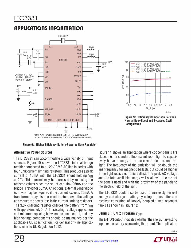
LTC3331
283331fa
For more information www.linear.com/LTC3331
Figure 9a. Higher Efficiency Battery-Powered Buck Regulator
Figure 9b. Efficiency Comparison Between Normal Buck-Boost and Bypassed SWB Configuration
APPLICATIONS INFORMATION
Alternative Power Sources
The LTC3331 can accommodate a wide variety of input sources. Figure 10 shows the LTC3331 internal bridge rectifier connected to a 120V RMS AC line in series with four 3.9k current limiting resistors. This produces a peak current of 10mA with the LTC3331 shunt holding VIN at 20V. This current may be increased by reducing the resistor values since the shunt can sink 25mA and the bridge is rated for 50mA. An optional external Zener diode (shown) may be required if the current exceeds 25mA. A transformer may also be used to step down the voltage and reduce the power loss in the current limiting resistors. The 3.3k charging resistor charges the battery from VIN with approximately 5mA. This is a high voltage application and minimum spacing between the line, neutral, and any high voltage components should be maintained per the applicable UL specification. For general off-line applica-tions refer to UL Regulation 1012.
Figure 11 shows an application where copper panels are placed near a standard fluorescent room light to capaci-tively harvest energy from the electric field around the light. The frequency of the emission will be double the line frequency for magnetic ballasts but could be higher if the light uses electronic ballast. The peak AC voltage and the total available energy will scale with the size of the panels used and with the proximity of the panels to the electric field of the light.
The LTC3331 could also be used to wirelessly harvest energy and charge a battery by using a transmitter and receiver consisting of loosely coupled tuned resonant tanks as shown in Figure 12.
Using EH_ON to Program VOUT
The EH_ON output indicates whether the energy harvesting input or the battery is powering the output. The application
LTC3331
3331 F09a
AC1VIN
CAP
VIN2
AC2
SWA
SWB
SW
1.8VVOUT
SCAP
BAL
PGVOUT
EH_ON
VIN3
IPK2
IPK1
IPK0
OUT2
OUT1
OUT0
22µH
UVLO RISING = 12V*UVLO FALLING = 11VIPEAK_BB = 250mA
22µF25V
1µF6.3V
4.7µF6.3V
UV3
UV2
UV1
UV0
BB_IN
BAT_IN
BAT_OUT
CHARGE
FLOAT0 FLOAT1 LBSEL SHIP GND
22µH
22µF6.3V
22µF6.3V
MIDE V25W
68k
4.0V
*FOR PEAK POWER TRANSFER, CENTER THE UVLO WINDOW AT HALF THE RECTIFIED OPEN CIRCUIT VOLTAGE OF THE PIEZO
0.1µF6.3V
Li-ION+ 1µF
6.3V
BB_IN (V)2.6
EFFI
CIEN
CY (%
)
90
95
100
3.2 3.6 4.2
3331 F09b
85
80
752.8 3 3.4 3.8 4
VOUT = 1.8V, BYPASS SWBVOUT = 1.8V, INCLUDE SWBVOUT = 3.3V, BYPASS SWBVOUT = 3.3V, INCLUDE SWB
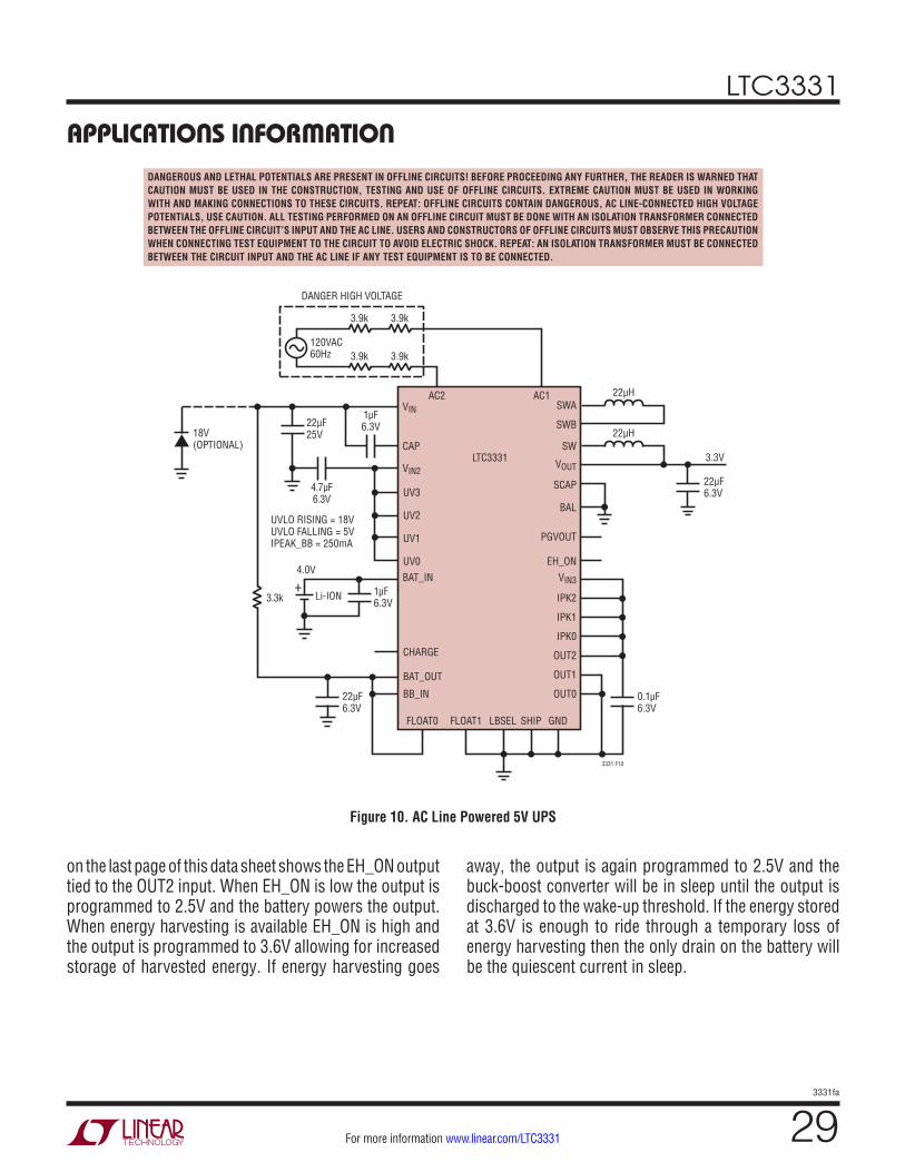
LTC3331
293331fa
For more information www.linear.com/LTC3331
DANGEROUS AND LETHAL POTENTIALS ARE PRESENT IN OFFLINE CIRCUITS! BEFORE PROCEEDING ANY FURTHER, THE READER IS WARNED THAT CAUTION MUST BE USED IN THE CONSTRUCTION, TESTING AND USE OF OFFLINE CIRCUITS. EXTREME CAUTION MUST BE USED IN WORKING WITH AND MAKING CONNECTIONS TO THESE CIRCUITS. REPEAT: OFFLINE CIRCUITS CONTAIN DANGEROUS, AC LINE-CONNECTED HIGH VOLTAGE POTENTIALS, USE CAUTION. ALL TESTING PERFORMED ON AN OFFLINE CIRCUIT MUST BE DONE WITH AN ISOLATION TRANSFORMER CONNECTED BETWEEN THE OFFLINE CIRCUIT’S INPUT AND THE AC LINE. USERS AND CONSTRUCTORS OF OFFLINE CIRCUITS MUST OBSERVE THIS PRECAUTION WHEN CONNECTING TEST EQUIPMENT TO THE CIRCUIT TO AVOID ELECTRIC SHOCK. REPEAT: AN ISOLATION TRANSFORMER MUST BE CONNECTED BETWEEN THE CIRCUIT INPUT AND THE AC LINE IF ANY TEST EQUIPMENT IS TO BE CONNECTED.
Figure 10. AC Line Powered 5V UPS
APPLICATIONS INFORMATION
LTC3331
3331 F10
AC1VIN
CAP
VIN2
AC2
3.9k3.9k120VAC60Hz
SWA
SWB
SW
VOUT
VIN3
SCAP
BAL
PGVOUT
OUT2
OUT1
OUT0
EH_ON
IPK2
IPK1
IPK0
UVLO RISING = 18VUVLO FALLING = 5VIPEAK_BB = 250mA
22µF25V
1µF6.3V
4.7µF6.3V
3.3k
UV3
UV2
UV1
UV0
BAT_IN
FLOAT0 FLOAT1 LBSEL SHIP GND
CHARGE
BB_IN
BAT_OUT
22µF6.3V
0.1µF6.3V
18V(OPTIONAL)
3.3V
22µF6.3V
22µH
22µH
3.9k3.9k
DANGER HIGH VOLTAGE
4.0V
Li-ION+ 1µF
6.3V
on the last page of this data sheet shows the EH_ON output tied to the OUT2 input. When EH_ON is low the output is programmed to 2.5V and the battery powers the output. When energy harvesting is available EH_ON is high and the output is programmed to 3.6V allowing for increased storage of harvested energy. If energy harvesting goes
away, the output is again programmed to 2.5V and the buck-boost converter will be in sleep until the output is discharged to the wake-up threshold. If the energy stored at 3.6V is enough to ride through a temporary loss of energy harvesting then the only drain on the battery will be the quiescent current in sleep.
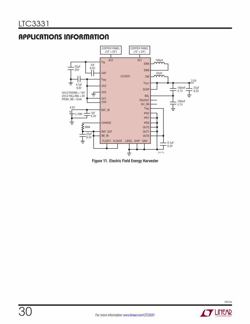
LTC3331
303331fa
For more information www.linear.com/LTC3331
Figure 11. Electric Field Energy Harvester
APPLICATIONS INFORMATION
LTC3331
3331 F10
AC1VIN
CAP
VIN2
AC2
COPPER PANEL(12" × 24")
SWA
VOUT
SW
SWB
SCAP
BAL
PGVOUTEH_ON
IPK2
IPK1
IPK0
OUT2OUT1OUT0
VIN3
UVLO RISING = 14VUVLO FALLING = 5VIPEAK_BB = 5mA
22µF25V
1µF6.3V
4.7µF6.3V
UV3
UV2
UV1UV0
BAT_IN
FLOAT1 FLOAT0 LBSEL SHIP GND
CHARGE
BB_INBAT_OUT
0.1µF6.3V
300k
100mF2.7V
100mF2.7V
100µH
22µH
2.5V
COPPER PANEL(12" × 24")
22µF6.3V
22µF6.3V
4.2V
Li-ION+ 1µF
6.3V
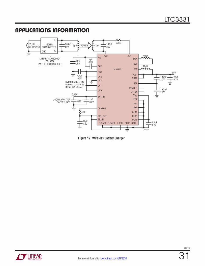
LTC3331
313331fa
For more information www.linear.com/LTC3331
Figure 12. Wireless Battery Charger
APPLICATIONS INFORMATION
LTC3331
3331 F12
AC1VIN
CAP
VIN2
AC2SWA
VOUT
SW
SWB
SCAP
BAL
PGVOUT
EH_ON
IPK2
IPK1IPK0
OUT2
OUT1OUT0
VIN3
UVLO RISING = 14VUVLO FALLING = 5VIPEAK_BB = 5mA
22µF25V
1µF6.3V
4.7µF6.3V
UV3
UV2
UV1
UV0
BAT_IN
FLOAT1 FLOAT0 LBSEL SHIP GND
CHARGE
BB_INBAT_OUT
0.1µF6.3V
4.3k
100mF2.7V
100mF2.7V
100µH
270Ω
22µH
2.5V
22µF6.3V
22µF6.3V
3.45V
Li-ION CAPACITORTAIYO YUDEN
200F 1µF6.3V
100nF25V47µH5µH POWER300nF
50VDCSOURCE
+–130kHz
TRANSMITTER
LINEAR TECHNOLOGYDC1968A
PART OF DC1969A-B KIT
GND
TX
TY
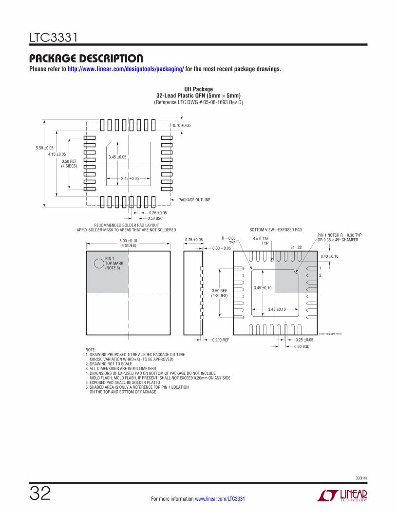
LTC3331
323331fa
For more information www.linear.com/LTC3331
PACKAGE DESCRIPTIONPlease refer to http://www.linear.com/designtools/packaging/ for the most recent package drawings.
5.00 ±0.10(4 SIDES)
NOTE:1. DRAWING PROPOSED TO BE A JEDEC PACKAGE OUTLINE M0-220 VARIATION WHHD-(X) (TO BE APPROVED)2. DRAWING NOT TO SCALE3. ALL DIMENSIONS ARE IN MILLIMETERS4. DIMENSIONS OF EXPOSED PAD ON BOTTOM OF PACKAGE DO NOT INCLUDE MOLD FLASH. MOLD FLASH, IF PRESENT, SHALL NOT EXCEED 0.20mm ON ANY SIDE5. EXPOSED PAD SHALL BE SOLDER PLATED6. SHADED AREA IS ONLY A REFERENCE FOR PIN 1 LOCATION ON THE TOP AND BOTTOM OF PACKAGE
PIN 1TOP MARK(NOTE 6)
0.40 ±0.10
31
1
2
32
BOTTOM VIEW—EXPOSED PAD
3.50 REF(4-SIDES)
3.45 ±0.10
3.45 ±0.10
0.75 ±0.05 R = 0.115TYP
0.25 ±0.05(UH32) QFN 0406 REV D
0.50 BSC
0.200 REF
0.00 – 0.05
0.70 ±0.05
3.50 REF(4 SIDES)
4.10 ±0.05
5.50 ±0.05
0.25 ±0.05
PACKAGE OUTLINE
0.50 BSC
RECOMMENDED SOLDER PAD LAYOUTAPPLY SOLDER MASK TO AREAS THAT ARE NOT SOLDERED
PIN 1 NOTCH R = 0.30 TYPOR 0.35 × 45° CHAMFERR = 0.05
TYP
3.45 ±0.05
3.45 ±0.05
UH Package32-Lead Plastic QFN (5mm × 5mm)
(Reference LTC DWG # 05-08-1693 Rev D)
LTC3331
333331fa
For more information www.linear.com/LTC3331
Information furnished by Linear Technology Corporation is believed to be accurate and reliable. However, no responsibility is assumed for its use. Linear Technology Corporation makes no representa-tion that the interconnection of its circuits as described herein will not infringe on existing patent rights.
REVISION HISTORYREV DATE DESCRIPTION PAGE NUMBER
A 07/14 Clarified IQ on the LTC3330 in the Related Parts list 34
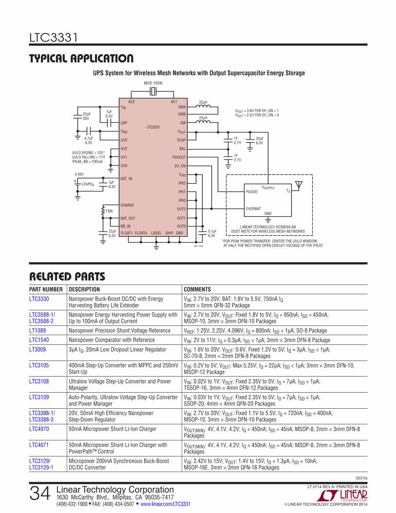
LTC3331
343331fa
For more information www.linear.com/LTC3331Linear Technology Corporation1630 McCarthy Blvd., Milpitas, CA 95035-7417
LINEAR TECHNOLOGY CORPORATION 2014
LT 0714 REV A• PRINTED IN USA
(408) 432-1900 FAX: (408) 434-0507 www.linear.com/LTC3331
UPS System for Wireless Mesh Networks with Output Supercapacitor Energy Storage
LTC3331
3331 TA02
AC1VIN
CAP
VIN2
AC2
SWB
SWA
SW
VOUT
SCAP
BAL
PGVOUT
EH_ON
IPK2
IPK1
IPK0
OUT2
OUT0
OUT1
VIN3
0.1µF6.3V
UVLO RISING = 12V*UVLO FALLING = 11VIPEAK_BB = 100mA
22µF25V
1µF6.3V
4.7µF6.3V
UV3
UV2
UV1
UV0
BAT_IN
FLOAT1 FLOAT0 LBSEL SHIP GND
CHARGE130k
BB_IN
BAT_OUT
LINEAR TECHNOLOGY DC9003A-ABDUST MOTE FOR WIRELESS MESH NETWORKS
PGOOD
EHORBAT
TXVSUPPLY
GND
VOUT = 3.6V FOR EH_ON = 1VOUT = 2.5V FOR EH_ON = 0
1F2.7V
1F2.7V
22µF6.3V
22µH
22µH
*FOR PEAK POWER TRANSFER, CENTER THE UVLO WINDOW AT HALF THE RECTIFIED OPEN CIRCUIT VOLTAGE OF THE PIEZO
22µF6.3V
3.45V
LiFePO4+ 1µF
6.3V
MIDE V25W
RELATED PARTS
TYPICAL APPLICATION
PART NUMBER DESCRIPTION COMMENTS
LTC3330 Nanopower Buck-Boost DC/DC with Energy Harvesting Battery Life Extender
VIN: 2.7V to 20V; BAT: 1.8V to 5.5V, 750nA IQ 5mm × 5mm QFN-32 Package
LTC3588-1/ LTC3588-2
Nanopower Energy Harvesting Power Supply with Up to 100mA of Output Current
VIN: 2.7V to 20V; VOUT: Fixed 1.8V to 5V; IQ = 950nA; ISD = 450nA; MSOP-10, 3mm × 3mm DFN-10 Packages
LT1389 Nanopower Precision Shunt Voltage Reference VREF: 1.25V, 2.25V, 4.096V; IQ = 800nA; ISD < 1µA; SO-8 Package
LTC1540 Nanopower Comparator with Reference VIN: 2V to 11V; IQ = 0.3µA; ISD < 1µA; 3mm × 3mm DFN-8 Package
LT3009 3μA IQ, 20mA Low Dropout Linear Regulator VIN: 1.6V to 20V; VOUT: 0.6V, Fixed 1.2V to 5V; IQ = 3µA; ISD < 1µA; SC-70-8, 2mm × 2mm DFN-8 Packages
LTC3105 400mA Step-Up Converter with MPPC and 250mV Start-Up
VIN: 0.2V to 5V; VOUT: Max 5.25V; IQ = 22µA; ISD < 1µA; 3mm × 3mm DFN-10, MSOP-12 Package
LTC3108 Ultralow Voltage Step-Up Converter and Power Manager
VIN: 0.02V to 1V; VOUT: Fixed 2.35V to 5V; IQ = 7µA; ISD < 1µA; TSSOP-16, 3mm × 4mm DFN-12 Packages
LTC3109 Auto-Polarity, Ultralow Voltage Step-Up Converter and Power Manager
VIN: 0.03V to 1V; VOUT: Fixed 2.35V to 5V; IQ = 7µA; ISD < 1µA; SSOP-20, 4mm × 4mm QFN-20 Packages
LTC3388-1/LTC3388-3
20V, 50mA High Efficiency Nanopower Step-Down Regulator
VIN: 2.7V to 20V; VOUT: Fixed 1.1V to 5.5V; IQ = 720nA; ISD = 400nA; MSOP-10, 3mm × 3mm DFN-10 Packages
LTC4070 50mA Micropower Shunt Li-Ion Charger VOUT(MIN): 4V, 4.1V, 4.2V; IQ = 450nA; ISD = 45nA; MSOP-8, 2mm × 3mm DFN-8 Packages
LTC4071 50mA Micropower Shunt Li-Ion Charger with PowerPath™ Control
VOUT(MIN): 4V, 4.1V, 4.2V; IQ = 450nA; ISD = 45nA; MSOP-8, 2mm × 3mm DFN-8 Packages
LTC3129/ LTC3129-1
Micropower 200mA Synchronous Buck-Boost DC/DC Converter
VIN: 2.42V to 15V; VOUT: 1.4V to 15V; IQ = 1.3µA; ISD = 10nA; MSOP-16E, 3mm × 3mm QFN-16 Packages