ltc2873 - single-bus rs485/rs232 multiprotocol …€¦ · loopback mode steers the driver inputs...
TRANSCRIPT
LTC2873
12873fa
For more information www.linear.com/LTC2873
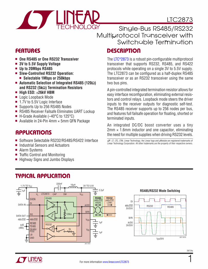
Typical applicaTion
FeaTures DescripTion
Single-Bus RS485/RS232 Multiprotocol Transceiver with
Switchable Termination
The LTC®2873 is a robust pin-configurable multiprotocol transceiver that supports RS232, RS485, and RS422 protocols while operating on a single 3V to 5.5V supply. The LTC2873 can be configured as a half-duplex RS485 transceiver or as an RS232 transceiver using the same two bus pins.
A pin-controlled integrated termination resistor allows for easy interface reconfiguration, eliminating external resis-tors and control relays. Loopback mode steers the driver inputs to the receiver outputs for diagnostic self-test. The RS485 receiver supports up to 256 nodes per bus, and features full failsafe operation for floating, shorted or terminated inputs.
An integrated DC/DC boost converter uses a tiny 2mm × 1.6mm inductor and one capacitor, eliminating the need for multiple supplies when driving RS232 levels.applicaTions
n One RS485 or One RS232 Transceiver n 3V to 5.5V Supply Voltage n Up to 20Mbps RS485 n Slew-Controlled RS232 Operation:
n Selectable 1Mbps or 250kbps n Automatic Selection of Integrated RS485 (120Ω)
and RS232 (5kΩ) Termination Resistors n High ESD: ±26kV HBM n Logic Loopback Mode n 1.7V to 5.5V Logic Interface n Supports Up to 256 RS485 Nodes n RS485 Receiver Failsafe Eliminates UART Lockup n H-Grade Available (–40°C to 125°C) n Available in 24-Pin 4mm × 5mm QFN Package
n Software Selectable RS232/RS485/RS422 Interface n Industrial Sensors and Actuators n Alarm Systems n Traffic Control and Monitoring n Highway Signs and Jumbo Displays
L, LT, LTC, LTM, Linear Technology, the Linear logo and µModule are registered trademarks of Linear Technology Corporation. All other trademarks are the property of their respective owners.
2873 TA01
120Ω
5k1μF
1μF
1μF
1.7V TO VCC 3V TO 5.5V220nF 10μH
2.2μF
VL CAP SW
SHDN
DI
RO
485/232485/232
D/R(485)
RE485TE485DE485/F232LBGND
RS232
RS485
A/DO
B/RI
VDD
VEE
VCC
DATA IN
DATA OUT
LTC2873
RS232(485/232
LOW)
RS485(485/232
HIGH)
RS485/RS232 Mode Switching
RS232 RS485
1µs/DIV
DI
485/2325V/DIV
A/DO3V/DIV
B/RI
2873 TA01b
LTC2873
22873fa
For more information www.linear.com/LTC2873
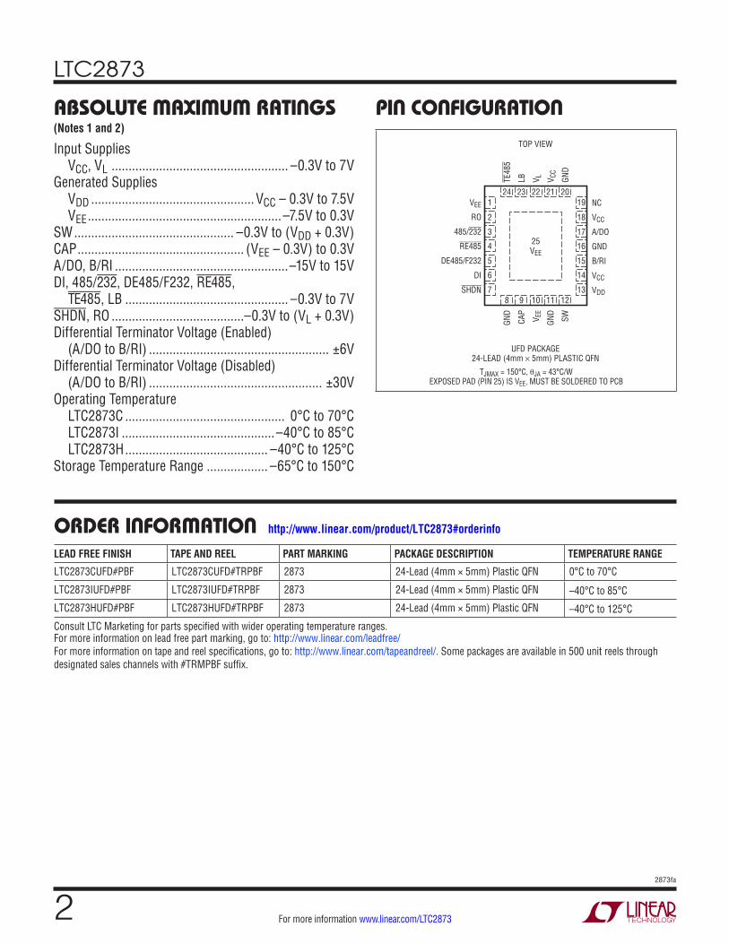
pin conFiguraTionabsoluTe MaxiMuM raTings
Input Supplies VCC, VL .................................................... –0.3V to 7VGenerated Supplies VDD ................................................ VCC – 0.3V to 7.5V VEE .........................................................–7.5V to 0.3VSW ............................................... –0.3V to (VDD + 0.3V)CAP ................................................. (VEE – 0.3V) to 0.3VA/DO, B/RI ...................................................–15V to 15VDI, 485/232, DE485/F232, RE485,
TE485, LB ................................................ –0.3V to 7VSHDN, RO .......................................–0.3V to (VL + 0.3V)Differential Terminator Voltage (Enabled) (A/DO to B/RI) ..................................................... ±6VDifferential Terminator Voltage (Disabled) (A/DO to B/RI) ................................................... ±30VOperating Temperature LTC2873C ............................................... 0°C to 70°C LTC2873I .............................................–40°C to 85°C LTC2873H .......................................... –40°C to 125°CStorage Temperature Range .................. –65°C to 150°C
(Notes 1 and 2)
8 9
TOP VIEW
UFD PACKAGE24-LEAD (4mm × 5mm) PLASTIC QFN
10 11 12
24 23 22 21 20
6
5
4
3
2
1VEE
RO
485/232
RE485
DE485/F232
DI
SHDN
NC
VCC
A/DO
GND
B/RI
VCC
VDD
TE48
5
LB V L V CC
GND
GND
CAP
V EE
GND
SW
7
14
15
16
17
18
19
13
25VEE
TJMAX = 150°C, θJA = 43°C/W
EXPOSED PAD (PIN 25) IS VEE, MUST BE SOLDERED TO PCB
orDer inForMaTionLEAD FREE FINISH TAPE AND REEL PART MARKING PACKAGE DESCRIPTION TEMPERATURE RANGE
LTC2873CUFD#PBF LTC2873CUFD#TRPBF 2873 24-Lead (4mm × 5mm) Plastic QFN 0°C to 70°C
LTC2873IUFD#PBF LTC2873IUFD#TRPBF 2873 24-Lead (4mm × 5mm) Plastic QFN –40°C to 85°C
LTC2873HUFD#PBF LTC2873HUFD#TRPBF 2873 24-Lead (4mm × 5mm) Plastic QFN –40°C to 125°C
Consult LTC Marketing for parts specified with wider operating temperature ranges. For more information on lead free part marking, go to: http://www.linear.com/leadfree/ For more information on tape and reel specifications, go to: http://www.linear.com/tapeandreel/. Some packages are available in 500 unit reels through designated sales channels with #TRMPBF suffix.
http://www.linear.com/product/LTC2873#orderinfo
LTC2873
32873fa
For more information www.linear.com/LTC2873
The l denotes the specifications which apply over the full operating temperature range, otherwise specifications are at TA = 25°C. VCC = VL = 3.3V, TE485 = VL, LB = 0V unless otherwise noted. (Notes 2, 6)
SYMBOL PARAMETER CONDITIONS MIN TYP MAX UNITS
Supplies
VCC Supply Voltage Operating Range l 3 5.5 V
VL Logic Supply Voltage Operating Range VL ≤ VCC l 1.7 VCC V
VCC Supply Current in Shutdown Mode SHDN = 0V l 8 30 µA
VCC Supply Current in RS232 Mode or RS485 Mode, Driver and Receiver Enabled, Termination Disabled
No Load, SHDN = TE485 = DE485/F232 = VL RE485 = 0
l 4 9 mA
VCC Supply Current in RS485 Mode with Receiver and Termination Enabled, Driver Disabled
No Load, SHDN = 485/232 = VL DE485/F232 = RE485 = TE485 = 0
l 4 9 mA
VL Supply Current in Any Mode No Load l 0 5 µA
Power Supply Generator
VDD Regulated VDD Output Voltage SHDN = VL, No Load 7.0 V
VEE Regulated VEE Output Voltage SHDN = VL, No Load –6.3 V
RS485 Driver
|VOD| Differential Output Voltage RL = Open, VCC = 3V (Figure 1) RL = 27Ω, VCC = 4.5V (Figure 1) RL = 27Ω, VCC = 3V (Figure 1) RL = 50Ω, VCC = 3.13V (Figure 1)
l
l
l
l
2.1 1.5 2
VCC VCC VCC
V V V V
∆|VOD| Difference in Magnitude of Differential Output Voltage for Complementary Output States
RL = 27Ω, VCC = 3V (Figure 1) RL = 50Ω, VCC = 3.13V (Figure 1)
l
l
0.2 0.2
V
VOC Common Mode Output Voltage RL = 27Ω or 50Ω (Figure 1) l 3 V
∆|VOC| Difference in Magnitude of Common Mode Output Voltage for Complementary Output States
RL = 27Ω or 50Ω (Figure 1) l 0.2 V
IOSD485 Maximum Short-Circuit Current –7V ≤ VOUT ≤ 12V (Figure 2) l ±250 mA
RS485 Receiver
IIN485 Input Current (A/DO, B/RI) (A/DO or B/RI) = 12V or –7V, VCC = 0V or 3.3V (Figure 3)
l –100 125 µA
RIN485 Input Resistance (A/DO, B/RI) (A/DO or B/RI) = 12V or –7V, VCC = 0V or 3.3V (Figure 3)
125 kΩ
Differential Input Signal Threshold Voltage (A/DO to B/RI)
–7V ≤ (A/DO or B/RI) ≤ 12V l ±200 mV
Input Hysteresis B = 0V 220 mV
Differential Input Failsafe Rising Threshold Voltage –7V ≤ (A/DO or B/RI) ≤ 12V, (A/D0 – B/RI) Rising l –200 –70 –20 mV
Input DC Failsafe Hysteresis 40 mV
VOL Receiver Output Low Voltage Output Low, I(RO) = 3mA (Sinking), 3V ≤ VL ≤ 5.5V
l 0.4 V
Output Low, I(RO) = 1mA (Sinking), 1.7V ≤ VL < 3V
l 0.4 V
elecTrical characTerisTics
LTC2873
42873fa
For more information www.linear.com/LTC2873
SYMBOL PARAMETER CONDITIONS MIN TYP MAX UNITS
VOH Receiver Output High Voltage Output High, I(RO) = –3mA (Sourcing), 3V ≤ VL ≤ 5.5V
l VL – 0.4 V
Output High, I(RO) = –1mA (Sourcing), 1.7V ≤ VL < 3V
l VL – 0.4 V
Three-State (High Impedance) Output Current (RO) 0V ≤ RO ≤ VL, VL = 5.5V, RE485 = VL l 0 ±5 µA
Short-Circuit Current (RO) 0V ≤ RO ≤ VL, VL = 5.5V l ±135 mA
RTERM Terminating Resistor TE485 = 0V, VAB = 2V, VB = –7V, 0V, 10V (Figure 8)
l 108 120 156 Ω
RS232 Driver
VOLD Output Low Voltage RL = 3kΩ, VEE ≤ –6V l –5 –5.5 VEE V
VOHD Output High Voltage RL = 3kΩ, VDD ≥ 6.5V l 5 5.9 VDD V
Output Short-Circuit Current Driver Output = 0V l ±25 ±90 mA
RS232 Receiver
Input Threshold Voltage l 0.6 1.5 2.5 V
Input Hysteresis l 0.1 0.4 1.0 V
Output Low Voltage I(RO) = 1mA (Sinking), 1.7V ≤ VL < 5.5V l 0.4 V
Output High Voltage I(RO) = –1mA (Sourcing), 1.7V ≤ VL < 5.5V l VL – 0.4 V
Input Resistance –15V ≤ B/RI ≤ 15V, 485/232 = 0V l 3 5 7 kΩ
Output Short-Circuit Current VL = 5.5V, 0V ≤ RO ≤ VL l ±25 ±50 mA
Logic Inputs
Threshold Voltage l 0.4 0.75 • VL V
Input Current l 0 ±5 µA
ESD
Interface Pins (A/DO, B/RI) Human Body Model to GND or VCC, Powered or Unpowered (Note 5)
±26 kV
All Other Pins Human Body Model (Note 5) ±4 kV
The l denotes the specifications which apply over the full operating temperature range, otherwise specifications are at TA = 25°C. VCC = VL = 3.3V, TE485 = VL, LB = 0V unless otherwise noted. (Notes 2, 6)elecTrical characTerisTics
LTC2873
52873fa
For more information www.linear.com/LTC2873
SYMBOL PARAMETER CONDITIONS MIN TYP MAX UNITS
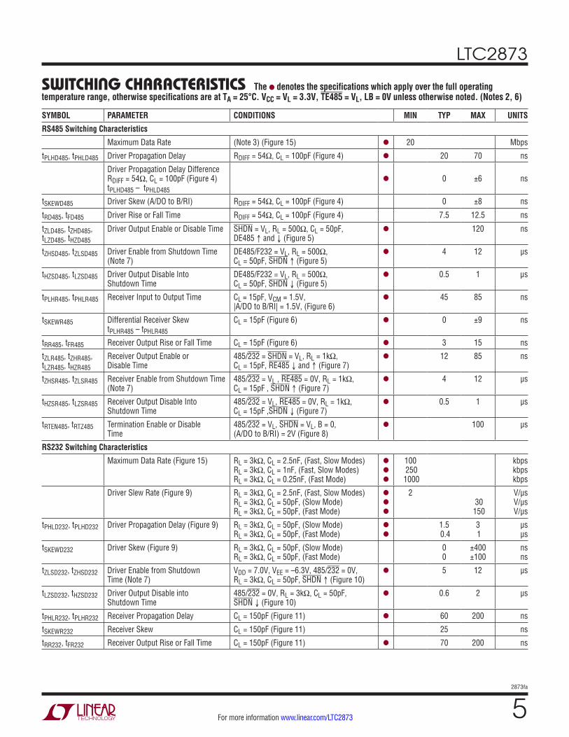
RS485 Switching Characteristics
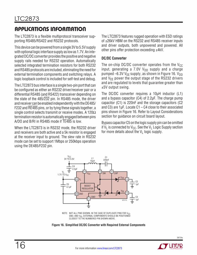
Maximum Data Rate (Note 3) (Figure 15) l 20 Mbps
tPLHD485, tPHLD485 Driver Propagation Delay RDIFF = 54Ω, CL = 100pF (Figure 4) l 20 70 ns
Driver Propagation Delay Difference RDIFF = 54Ω, CL = 100pF (Figure 4) tPLHD485 – tPHLD485
l
0
±6
ns
tSKEWD485 Driver Skew (A/DO to B/RI) RDIFF = 54Ω, CL = 100pF (Figure 4) 0 ±8 ns
tRD485, tFD485 Driver Rise or Fall Time RDIFF = 54Ω, CL = 100pF (Figure 4) 7.5 12.5 ns
tZLD485, tZHD485, tLZD485, tHZD485
Driver Output Enable or Disable Time SHDN = VL, RL = 500Ω, CL = 50pF, DE485 ↑ and ↓ (Figure 5)
l 120 ns
tZHSD485, tZLSD485 Driver Enable from Shutdown Time (Note 7)
DE485/F232 = VL, RL = 500Ω, CL = 50pF, SHDN ↑ (Figure 5)
l 4 12 µs
tHZSD485, tLZSD485 Driver Output Disable Into Shutdown Time
DE485/F232 = VL, RL = 500Ω, CL = 50pF, SHDN ↓ (Figure 5)
l 0.5 1 μs
tPLHR485, tPHLR485 Receiver Input to Output Time CL = 15pF, VCM = 1.5V, |A/DO to B/RI| = 1.5V, (Figure 6)
l 45 85 ns
tSKEWR485 Differential Receiver Skew tPLHR485 – tPHLR485
CL = 15pF (Figure 6) l 0 ±9 ns
tRR485, tFR485 Receiver Output Rise or Fall Time CL = 15pF (Figure 6) l 3 15 ns
tZLR485, tZHR485, tLZR485, tHZR485
Receiver Output Enable or Disable Time
485/232 = SHDN = VL, RL = 1kΩ, CL = 15pF, RE485 ↓ and ↑ (Figure 7)
l 12 85 ns
tZHSR485, tZLSR485 Receiver Enable from Shutdown Time (Note 7)
485/232 = VL , RE485 = 0V, RL = 1kΩ, CL = 15pF , SHDN ↑ (Figure 7)
l 4 12 µs
tHZSR485, tLZSR485 Receiver Output Disable Into Shutdown Time
485/232 = VL, RE485 = 0V, RL = 1kΩ, CL = 15pF ,SHDN ↓ (Figure 7)
l 0.5 1 µs
tRTEN485, tRTZ485 Termination Enable or Disable Time
485/232 = VL, SHDN = VL, B = 0, (A/DO to B/RI) = 2V (Figure 8)
l 100 µs
RS232 Switching Characteristics
Maximum Data Rate (Figure 15) RL = 3kΩ, CL = 2.5nF, (Fast, Slow Modes) RL = 3kΩ, CL = 1nF, (Fast, Slow Modes) RL = 3kΩ, CL = 0.25nF, (Fast Mode)
l
l
l
100 250
1000
kbps kbps kbps
Driver Slew Rate (Figure 9) RL = 3kΩ, CL = 2.5nF, (Fast, Slow Modes) RL = 3kΩ, CL = 50pF, (Slow Mode) RL = 3kΩ, CL = 50pF, (Fast Mode)
l
l
l
2 30
150
V/µs V/µs V/µs
tPHLD232, tPLHD232 Driver Propagation Delay (Figure 9) RL = 3kΩ, CL = 50pF, (Slow Mode) RL = 3kΩ, CL = 50pF, (Fast Mode)
l
l
1.5 0.4
3 1
µs µs
tSKEWD232 Driver Skew (Figure 9) RL = 3kΩ, CL = 50pF, (Slow Mode) RL = 3kΩ, CL = 50pF, (Fast Mode)
0 0
±400 ±100
ns ns
tZLSD232, tZHSD232 Driver Enable from Shutdown Time (Note 7)
VDD = 7.0V, VEE = –6.3V, 485/232 = 0V, RL = 3kΩ, CL = 50pF, SHDN ↑ (Figure 10)
l 5 12 µs
tLZSD232, tHZSD232 Driver Output Disable into Shutdown Time
485/232 = 0V, RL = 3kΩ, CL = 50pF, SHDN ↓ (Figure 10)
l 0.6 2 µs
tPHLR232, tPLHR232 Receiver Propagation Delay CL = 150pF (Figure 11) l 60 200 ns
tSKEWR232 Receiver Skew CL = 150pF (Figure 11) 25 ns
tRR232, tFR232 Receiver Output Rise or Fall Time CL = 150pF (Figure 11) l 70 200 ns
The l denotes the specifications which apply over the full operating temperature range, otherwise specifications are at TA = 25°C. VCC = VL = 3.3V, TE485 = VL, LB = 0V unless otherwise noted. (Notes 2, 6)swiTching characTerisTics
LTC2873
62873fa
For more information www.linear.com/LTC2873
The l denotes the specifications which apply over the full operating temperature range, otherwise specifications are at TA = 25°C. VCC = VL = 3.3V, TE485 = VL, LB = 0V unless otherwise noted. (Notes 2, 6)swiTching characTerisTics
SYMBOL PARAMETER CONDITIONS MIN TYP MAX UNITS
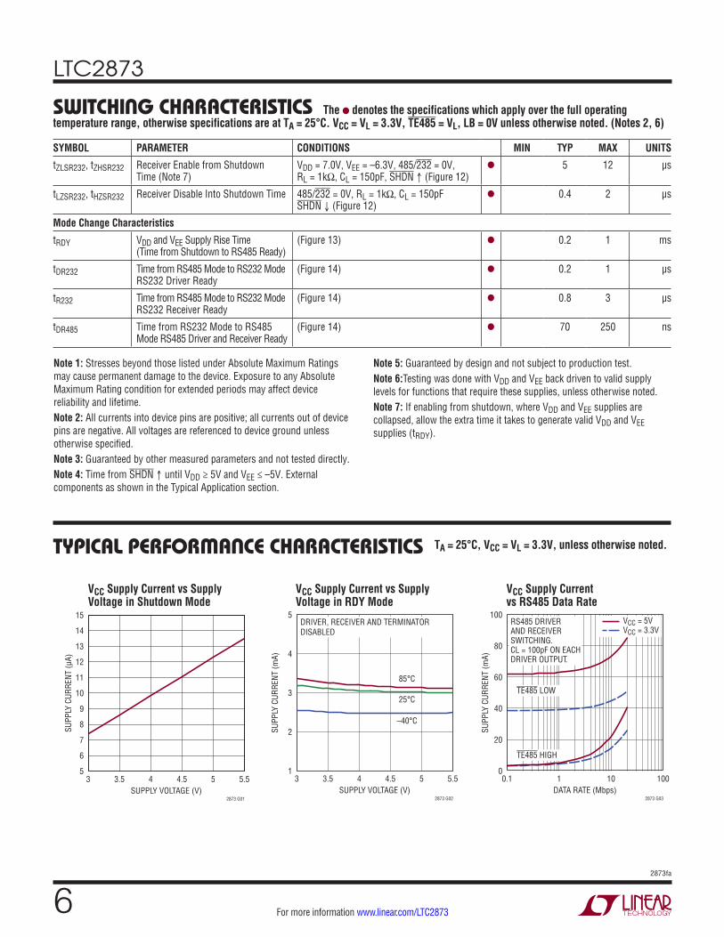
tZLSR232, tZHSR232 Receiver Enable from Shutdown Time (Note 7)
VDD = 7.0V, VEE = –6.3V, 485/232 = 0V, RL = 1kΩ, CL = 150pF, SHDN ↑ (Figure 12)
l 5 12 µs
tLZSR232, tHZSR232 Receiver Disable Into Shutdown Time 485/232 = 0V, RL = 1kΩ, CL = 150pF SHDN ↓ (Figure 12)
l 0.4 2 μs
Mode Change Characteristics
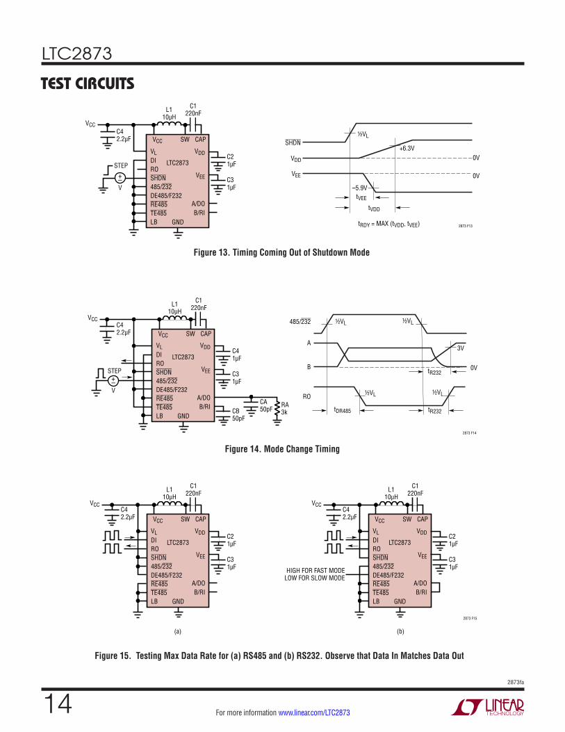
tRDY VDD and VEE Supply Rise Time (Time from Shutdown to RS485 Ready)
(Figure 13) l 0.2 1 ms
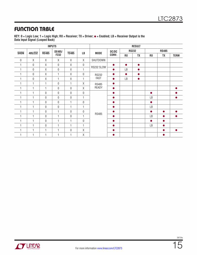
tDR232 Time from RS485 Mode to RS232 Mode RS232 Driver Ready
(Figure 14) l 0.2 1 µs
tR232 Time from RS485 Mode to RS232 Mode RS232 Receiver Ready
(Figure 14) l 0.8 3 µs
tDR485 Time from RS232 Mode to RS485 Mode RS485 Driver and Receiver Ready
(Figure 14) l 70 250 ns
Note 1: Stresses beyond those listed under Absolute Maximum Ratings may cause permanent damage to the device. Exposure to any Absolute Maximum Rating condition for extended periods may affect device reliability and lifetime.Note 2: All currents into device pins are positive; all currents out of device pins are negative. All voltages are referenced to device ground unless otherwise specified.Note 3: Guaranteed by other measured parameters and not tested directly.Note 4: Time from SHDN ↑ until VDD ≥ 5V and VEE ≤ –5V. External components as shown in the Typical Application section.
Note 5: Guaranteed by design and not subject to production test.Note 6:Testing was done with VDD and VEE back driven to valid supply levels for functions that require these supplies, unless otherwise noted.Note 7: If enabling from shutdown, where VDD and VEE supplies are collapsed, allow the extra time it takes to generate valid VDD and VEE supplies (tRDY).
VCC Supply Current vs Supply Voltage in Shutdown Mode
VCC Supply Current vs Supply Voltage in RDY Mode
VCC Supply Current vs RS485 Data Rate
Typical perForMance characTerisTics TA = 25°C, VCC = VL = 3.3V, unless otherwise noted.
SUPPLY VOLTAGE (V)3 3.5 4 4.5 5 5.5
5
6
7
8
9
10
11
12
13
14
15
SUPP
LY C
URRE
NT (μ
A)
2873 G01
SUPPLY VOLTAGE (V)3
SUPP
LY C
URRE
NT (m
A)
5
4
3
2
14.5 53.5
2873 G02
5.54
–40°C
25°C
85°C
DRIVER, RECEIVER AND TERMINATORDISABLED
DATA RATE (Mbps)0.1
SUPP
LY C
URRE
NT (m
A)
100
80
60
40
20
010
2873 G03
1001
TE485 LOW
TE485 HIGH
VCC = 5VVCC = 3.3V
RS485 DRIVER AND RECEIVERSWITCHING.CL = 100pF ON EACHDRIVER OUTPUT.
LTC2873
72873fa
For more information www.linear.com/LTC2873
Typical perForMance characTerisTics TA = 25°C, VCC = VL = 3.3V, unless otherwise noted.
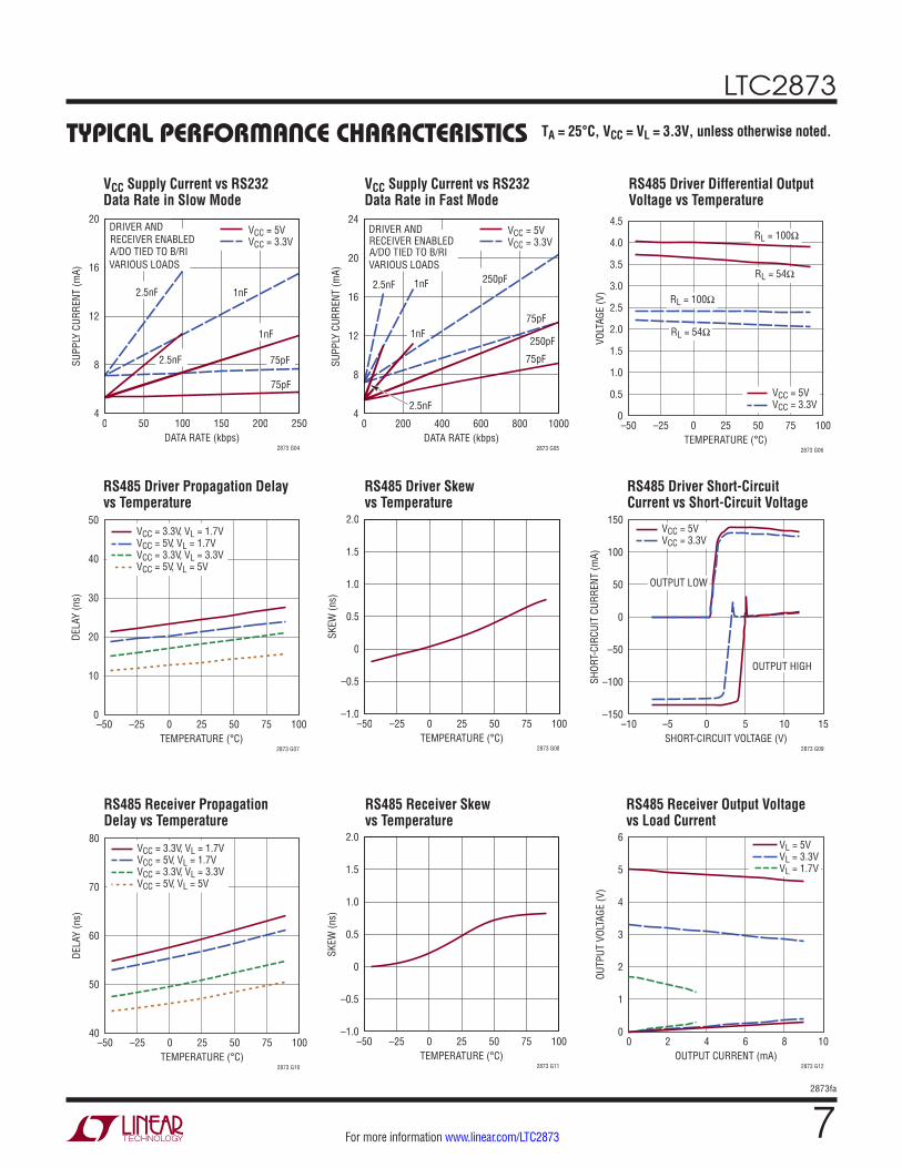
VCC Supply Current vs RS232 Data Rate in Slow Mode
VCC Supply Current vs RS232 Data Rate in Fast Mode
RS485 Driver Differential Output Voltage vs Temperature
RS485 Driver Propagation Delay vs Temperature
RS485 Driver Skew vs Temperature
RS485 Driver Short-Circuit Current vs Short-Circuit Voltage
RS485 Receiver Propagation Delay vs Temperature
RS485 Receiver Skew vs Temperature
RS485 Receiver Output Voltage vs Load Current
2.5nF
2.5nF
1nF
1nF
75pF
75pF
VARIOUS LOADSA/DO TIED TO B/RIRECEIVER ENABLEDDRIVER AND VCC = 5V
VCC = 3.3V
DATA RATE (kbps)0 50 100 150 200 250
4
8
12
16
20
SUPP
LY C
URRE
NT (m
A)
2873 G04
2.5nF
2.5nF
1nF
1nF75pF
75pF
VARIOUS LOADSA/DO TIED TO B/RIRECEIVER ENABLED
250pF
250pF
DRIVER AND VCC = 5VVCC = 3.3V
DATA RATE (kbps)0 200 400 600 800 1000
4
8
12
16
20
24
SUPP
LY C
URRE
NT (m
A)
2873 G05TEMPERATURE (°C)
–50
VOLT
AGE
(V)
4.5
3.5
2.5
1.5
4.0
3.0
2.0
1.0
0.5
050 75–25
2873 G06
100250
RL = 100Ω
RL = 54Ω
RL = 100Ω
RL = 54Ω
VCC = 5VVCC = 3.3V
TEMPERATURE (°C)–50
DELA
Y (n
s)
50
40
30
20
10
050 75–25
2873 G07
100250
VCC = 3.3V, VL = 1.7VVCC = 5V, VL = 1.7VVCC = 3.3V, VL = 3.3VVCC = 5V, VL = 5V
TEMPERATURE (°C)–50 –25 0 25 50 75 100
–1.0
–0.5
0
0.5
1.0
1.5
2.0
SKEW
(ns)
2873 G08SHORT-CIRCUIT VOLTAGE (V)
–10
SHOR
T-CI
RCUI
T CU
RREN
T (m
A)
150
100
0
50
–50
–100
–15010–5
2873 G09
1550
OUTPUT LOW
OUTPUT HIGH
VCC = 5VVCC = 3.3V
TEMPERATURE (°C)–50
DELA
Y (n
s)
80
70
60
50
4050 75–25
2873 G10
100250
VCC = 3.3V, VL = 1.7VVCC = 5V, VL = 1.7VVCC = 3.3V, VL = 3.3VVCC = 5V, VL = 5V
TEMPERATURE (°C)–50 –25 0 25 50 75 100
–1.0
–0.5
0
0.5
1.0
1.5
2.0
SKEW
(ns)
2873 G11OUTPUT CURRENT (mA)
0
OUTP
UT V
OLTA
GE (V
)
6
5
4
2
3
1
082
2873 G12
1064
VL = 5VVL = 3.3VVL = 1.7V
LTC2873
82873fa
For more information www.linear.com/LTC2873
Typical perForMance characTerisTics TA = 25°C, VCC = VL = 3.3V, unless otherwise noted.
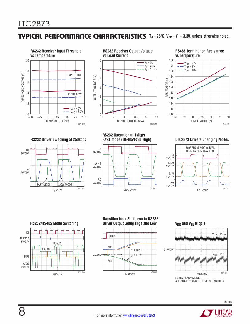
RS232 Receiver Input Threshold vs Temperature
RS232 Receiver Output Voltage vs Load Current
RS485 Termination Resistance vs Temperature
RS232 Driver Switching at 250kbpsRS232 Operation at 1Mbps FAST Mode (DE485/F232 High) LTC2873 Drivers Changing Modes
RS232/RS485 Mode SwitchingTransition from Shutdown to RS232 Driver Output Going High and Low VDD and VEE Ripple
TEMPERATURE (°C)–50
THRE
SHOL
D VO
LTAG
E (V
)
2.0
1.8
1.6
1.4
1.2
1.050 75–25
2873 G13
100250
VCC = 5VVCC = 3.3V
INPUT HIGH
INPUT LOW
OUTPUT CURRENT (mA)0
OUTP
UT V
OLTA
GE (V
)
6
5
4
2
3
1
082
2873 G14
1064
VL = 5VVL = 3.3VVL = 1.7V
TEMPERATURE (°C)–50
RESI
STAN
CE (Ω
)
130
118
116
114
112
110
128
126
124
122
120
50 75–25
2873 G15
100250
VCM = –7VVCM = 2VVCM = 12V
FAST MODE SLOW MODE
2µs/DIV
DI3V/DIV
A3V/DIV
2873 G16400ns/DIV
RO3V/DIV
DI3V/DIV
A = B3V/DIV
2873 G17
TERMINATION ENABLED50pF FROM A/DO to B/RI,
20ns/DIV
DI5V/DIV
RO5V/DIV
A/DO1V/DIV
B/RI1V/DIV
2873 G18
RS232
RS485
2µs/DIV
DI
485/2325V/DIV
A/DO3V/DIV
B/RI
2873 G19
A HIGH
A LOW
SHDN
VEE
VDD
40µs/DIV
3V/DIV
2873 G20
10mV/DIV
2873 G2140µs/DIVRS485 READY MODE,ALL DRIVERS AND RECEIVERS DISABLED
VDD RIPPLE
VEE RIPPLE
LTC2873
92873fa
For more information www.linear.com/LTC2873
pin FuncTionsVEE (Pins 1, 10, 25): Generated Negative Supply Voltage for RS232 Driver (–6.3V). Tie all pins together and connect 1µF capacitor between VEE (Pin 10) and GND. Exposed pad (Pin 25) must be soldered to PCB to maintain low thermal resistance.
RO (Pin 2): RS485 Differential Receiver Output and RS232 Receiver Output. Logic level referenced to GND and VL.
485/232 (Pin3): Interface Select Input. A logic low enables RS232 mode and a high enables RS485 mode. The mode determines which transceiver inputs and outputs are ac-cessible at the LTC2873 pins. Logic level referenced to GND and VL. Do not float.
RE485 (Pin4): RS485 Receiver Enable. In RS485 mode, a logic high disables the RS485 receiver, leaving its output Hi-Z and a logic low enables the RS485 receiver. This input has no function in RS232 mode (485/232 low). Logic level referenced to GND and VL. Do not float.
DE485/F232 (Pin 5): RS485 Driver Enable and RS232 Fast Mode Enable. In RS485 mode (485/232 high), a logic low disables the RS485 driver leaving the driver outputs in a Hi-Z state and a logic high enables the RS485 driver. In RS232 mode (485/232 low), a logic high enables Fast mode with maximum data rate of 1Mbps. A logic low enables Slow mode with a maximum data rate of 250kbps. Logic level referenced to GND and VL. Do not float.
DI (Pin 6): RS485 and RS232 Driver Input. Logic level referenced to GND and VL. Do not float.
SHDN (Pin7): Shutdown Control. A logic low disables the LTC2873 into low power shutdown state, independent of the other inputs. Driver and receiver outputs become Hi-Z. Logic level referenced to GND and VL. Do not float.
GND (Pin 8, 11, 16, 20): Ground. Tie all four pins together.
CAP (Pin 9): Charge Pump Capacitor for Generated Negative Supply Voltage VEE. Connect a 220nF capacitor between CAP and SW.
SW (Pin 12): Switch Pin. Connect 10µH inductor between SW and VCC. See Inductor Selection section for further details.
VDD (Pin 13): Generated Positive Supply Voltage for RS232 Driver (+7.0V). Connect 1µF capacitor between VDD and GND.
VCC (Pin 14, 18, 21): Input Supply (3V to 5.5V). Tie all three pins together and connect a 2.2µF or larger capacitor between VCC (adjacent to VDD) and GND.
B/RI (Pin 15): RS485 Negative Receiver Input and Driver Output. In RS232 mode, this is the RS232 receiver input.
A/DO (Pin 17): RS485 Positive Receiver Input and Driver Output. In RS232 mode, this is the RS232 driver output.
NC (Pin 19): Not connected internally.
VL (Pin 22): Logic Supply (1.7V to 5.5V) for the Receiver Outputs, Driver Inputs, and Control Inputs. Bypass this pin to GND with a 0.1µF capacitor if not tied to VCC. Keep VL ≤ VCC for operation guaranteed to meet specifications. However, VL > VCC will not damage the device, provided that absolute maximum limits are respected. See “VL Logic Supply and Logic Pins” in Applications section for more information.
LB (Pin 23): Loopback Enable. A logic high enables logic loopback diagnostic mode, internally routing the driver input logic signals to the receiver output pins. This applies to RS232 and RS485 operation. The targeted receiver must be enabled for the loopback signal to be available on its output. A logic low disables Loopback mode. In Loopback mode, signals are not inverted from driver inputs to receiver outputs. Logic level referenced to GND and VL. Do not float.
TE485 (Pin24): RS485 Termination Enable. In RS485 mode, a logic low enables a 120Ω resistor between pins A/DO and B/RI. A logic high opens the resistor between A/DO and B/RI, leaving the pins unterminated. In RS485 mode, the 5k resistor between B/RI and GND is never engaged. In RS232 mode, the 120Ω resistor between A/DO and B/RI is never engaged, regardless of the state of TE485, and the 5k resistor between B/RI and GND is always engaged. Logic level referenced to GND and VL. Do not float.

LTC2873
102873fa
For more information www.linear.com/LTC2873
block DiagraM
2873 BD
CONTROLLOGIC
DRIVERS
RECEIVERSLOOPBACK
PATH
0.1µF
SHDN
485/232
DE485/F232
RE485
TE485
LB
DI
RO
GND
B/RI
A/DO
VEE
VDD
1.7V TO 5.5V(≤ VCC)
PULSE-SKIPPINGBOOST
REGULATORf = 1.2MHz
RT232
RT485
2.2µF
10µH 220nF3V TO 5.5V
1µF
1µF
CAPSWVCCVL
232
485
232
485
5k
RT232
125k
RT485
120Ω
125k
LTC2873
112873fa
For more information www.linear.com/LTC2873
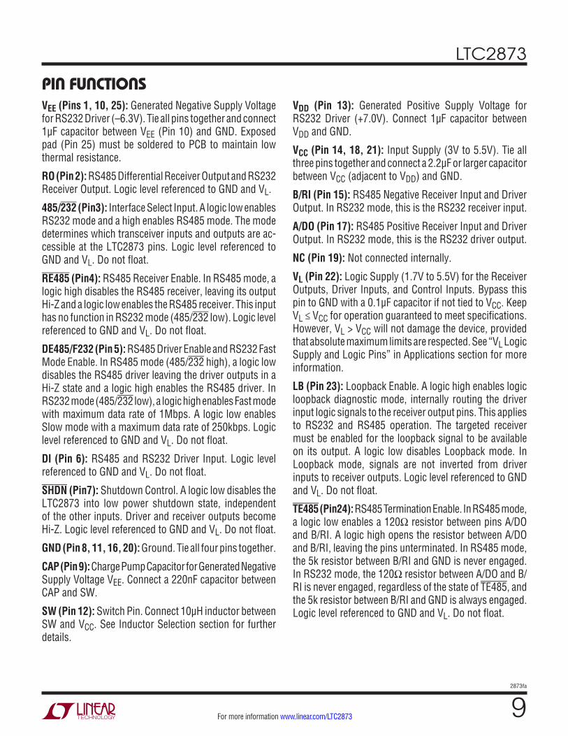
Figure 1. RS485 Driver DC Characteristics Figure 2. RS485 Driver Output Current
Figure 3. RS485 Receiver Input Current and Resistance
Figure 4. RS485 Driver Timing Measurement
TesT circuiTs
2873 F01
DRIVERDIGND
ORVL
A/DORL
RLB/RI
VOD
+
–VOC
+
–
2873 F02
DRIVER
A/DO OR B/RI
DIGND
ORVL B/RI
OR A/DOVOUT
IOSD485
+–
2873 F03
RECEIVER
VINIIN485
RIN485 =
VIN
IIN485
+–
A/DO OR B/RI
B/RI OR A/DO
2873 F04
DRIVERDI
A/DO
B/RI
RDIFF
CL
CL
tPLHD485
tSKEWD485
tPHLD485
tRD485 tFD485
90%0V
VOD ½VOD
VL
0V
DI
B/RI
A/DO
A/RO – B/DI10%
90%0V
10%
LTC2873
122873fa
For more information www.linear.com/LTC2873
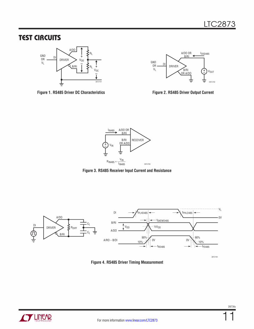
Figure 5. RS485 Driver Enable and Disable Timing Measurements
Figure 6. RS485 Receiver Propagation Delay Measurements
Figure 7. RS485 Receiver Enable and Disable Timing Measurements
TesT circuiTs
Figure 8. RS485 Termination Resistance and Timing Measurements
2873 F05
tZLD485,tZLSD485 tLZD485,
tLZSD485
tHZD485,tHZSD485
tZHD485,tZHSD485
½VCC
½VCC
VL
VOL
VCC
VOH
0V
0V
A/DO OR B/RI
B/RI OR A/DO
DRIVERDI
DE485/F232 OR SHDN
VLOR
GND
A/DO
RL
B/RI
GNDORVCC
VCCOR
GND
RL
CL
CL
½VL ½VLDE485/F232 OR SHDN
0.5V
0.5V
2873 F06
RECEIVERVCM
±VAB/2 A/DO
B/RI
RO
±VAB/2CL
tPLHR485
tSKEWR485 = tPLHR485 – tPHLR485
tRR485
90%
0V
½VL
A/DO TO B/RI
RO10%
tPHLR485
tFR485
90%
0V
–VAB
VAB
½VL 10%
VL
2873 F08
RECEIVER VAB
A/DO
B/RI
VAB
IARTERM =
VB
½VL ½VLTE485
IA
IA
90%10%
tRTZ485tRTEN4850V
VL
TE485
+–
+–
2873 F07
tZLR485,tZLRSR485
tLZR485,tLZSR485
tHZR485,tHZSR485
tZHR485,tZHRSR485
½VL
½VL
VL
VOL
VL
VOH
0V
0V
RE485 OR SHDN
RO
RO
RECEIVERRO
RE485 OR SHDN
0V TO 3V
3V TO 0V
A/DORL
B/RI
VLOR
GNDCL
½VL ½VL
0.5V
0.5V
LTC2873
132873fa
For more information www.linear.com/LTC2873
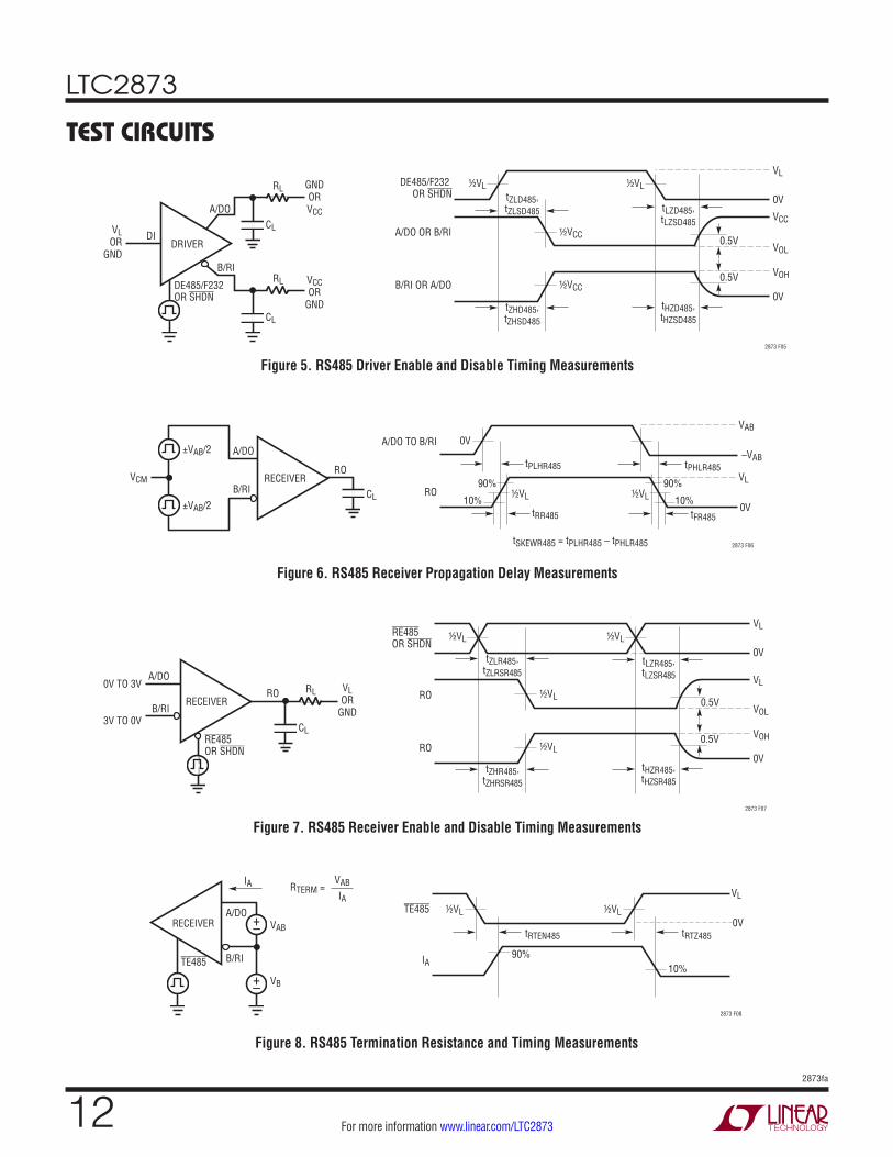
Figure 9. RS232 Driver Timing and Slew Rate Measurements
Figure 10. RS232 Driver Enable and Disable Times
TesT circuiTs
2873 F09
DI A/DO
CLRL
tPHLD232
tPLHD232
tSKEWD232 = |tPHLD232 – tPLHD232|
tF tR
DI
A/DO
SLEW RATE = 6V
tF OR tR
3V
–3V
0V
VOLD
VL
½VL ½VL
0V3V
–3V0V
VOHD
2873 F10
0V OR VL
SHDN
A/DO
CLRLtHZSD232
tLZSD232
SHDN
A/DO
A/DO
tZHSD232
tZLSD232
5V
–5V
0V
0V
0V
VOHD
VL
½VL ½VL
VOLD0.5V
0.5V
Figure 11. RS232 Receiver Timing Measurements
Figure 12. RS232 Receiver Enable and Disable Times
2873 F11
tPHLR232
tSKEWR232 = |tPLHR232 – tPHLR232|
tPLHR232
tRR232
90%
1.5V 1.5V
½VL 10%tFR232
90%
–3V
VL
+3V
½VL10% 0V
RO
RO
B/RI
B/RI
CL
2873 F12
–3V OR +3V
SHDN
RO GND
OR VL
CL
RL
tHZR232,tHZSR232
tLZR232,tLZSR232
SHDN
RO
RO
tZHR232,tZHSR232
tZLR232,
½VL
½VL
0V
0V
VL
VOHR
VL
½VL ½VL
VOLR
tZLSR232
0.5V
0.5V
LTC2873
142873fa
For more information www.linear.com/LTC2873
TesT circuiTs
SWVCC
C1220nFL1
10µH
LTC2873
VLDIRO
C42.2µF
2873 F13
SHDN485/232DE485/F232RE485TE485LB
VDD
VEE
VCC
CAP
B/RIA/DO
GND
C21µF
C31µF
+–V
tVEE
tVDD
SHDN
VDD
VEE
+6.3V
–5.9V
0V
½VL
0V
tRDY = MAX (tVDD, tVEE)
STEP
SWVCC
C1220nFL1
10µH
LTC2873
VLDIRO
C42.2µF
2873 F14
SHDN485/232DE485/F232RE485TE485LB
VDD
VEE
VCC
CAP
B/RIA/DO
GND
C41µF
C31µF
CB50pF
CA50pF
RA3k
+–V
tDR485
3V
0V
½VL ½VL
STEP
tR232
tR232
½VL ½VLRO
B
A
485/232
SWVCC
C1220nFL1
10µH
LTC2873
VLDIRO
C42.2µF
2873 F15
SHDN485/232DE485/F232RE485TE485LB
VDD
VEE
VCC
CAP
B/RIA/DO
GND
C21µF
C31µF
SWVCC
C1220nFL1
10µH
LTC2873
VLDIRO
C42.2µF
SHDN485/232DE485/F232RE485TE485LB
VDD
VEE
VCC
CAP
B/RIA/DO
GND
C21µF
C31µF
(a) (b)
HIGH FOR FAST MODELOW FOR SLOW MODE
Figure 13. Timing Coming Out of Shutdown Mode
Figure 14. Mode Change Timing
Figure 15. Testing Max Data Rate for (a) RS485 and (b) RS232. Observe that Data In Matches Data Out
LTC2873
152873fa
For more information www.linear.com/LTC2873
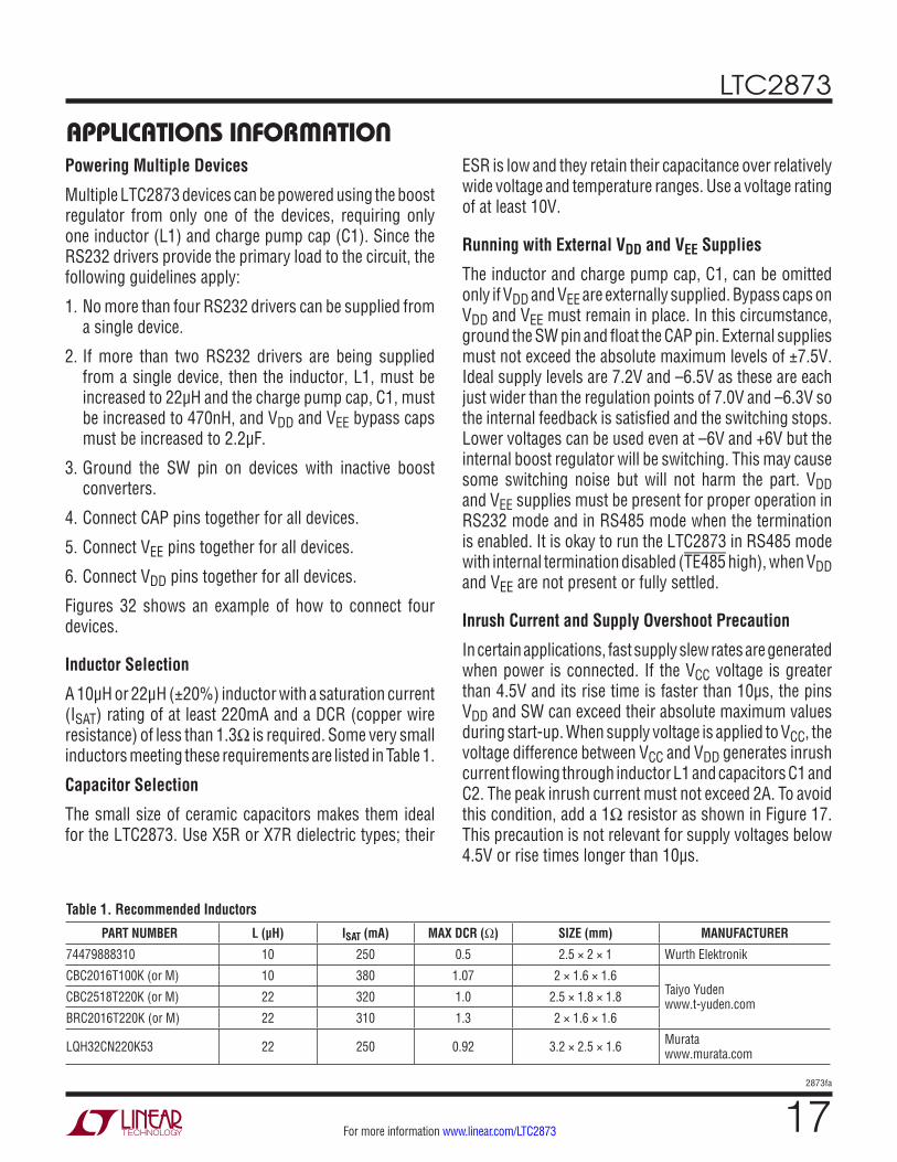
FuncTion TableKEY: 0 = Logic Low; 1 = Logic High; RX = Receiver; TX = Driver; l = Enabled; LB = Receiver Output is the Data Input Signal (Looped Back)
INPUTS RESULT
SHDN 485/232 RE485 DE485/F232 TE485 LB MODE DC/DC
CONV.RS232 RS485
RX TX RX TX TERM
0 X X X X X SHUTDOWN
1 0 X 0 X 0RS232 SLOW
l l l
1 0 X 0 X 1 l LB l
1 0 X 1 X 0 RS232 FAST
l l l
1 0 X 1 X 1 l LB l
1 1 1 0 1 X RS485 READY
l
1 1 1 0 0 X l l
1 1 0 0 0 0
RS485
l l l
1 1 0 0 0 1 l LB l
1 1 0 0 1 0 l l
1 1 0 0 1 1 l LB
1 1 0 1 0 0 l l l l
1 1 0 1 0 1 l LB l l
1 1 0 1 1 0 l l l
1 1 0 1 1 1 l LB l
1 1 1 1 0 X l l l
1 1 1 1 1 X l l
LTC2873
162873fa
For more information www.linear.com/LTC2873
Figure 16. Simplified DC/DC Converter with Required External Components
The LTC2873 is a flexible multiprotocol transceiver sup-porting RS485/RS422 and RS232 protocols.
This device can be powered from a single 3V to 5.5V supply with optional logic interface supply as low as 1.7V. An inte-grated DC/DC converter provides the positive and negative supply rails needed for RS232 operation. Automatically selected integrated termination resistors for both RS232 and RS485 protocols are included, eliminating the need for external termination components and switching relays. A logic loopback control is included for self-test and debug.
The LTC2873 bus interface is a single two-pin port that can be configured as either an RS232 driver/receiver pair or a differential RS485 (and RS422) transceiver depending on the state of the 485/232 pin. In RS485 mode, the driver and receiver can be enabled independently with the DE485/F232 and RE485 pins, or by tying these signals together, a single control selects transmit or receive modes. A 120Ω termination resistor is automatically engaged between pins A/DO and B/RI in RS485 mode if TE485 is low.
When the LTC2873 is in RS232 mode, the RS232 driver and receivers are both active and a 5k resistor is engaged at the receiver input to ground. The slew rate in RS232 mode can be set to support 1Mbps or 250kbps operation using the DE485/F232 pin.
applicaTions inForMaTionThe LTC2873 features rugged operation with ESD ratings of ±26kV HBM on the RS232 and RS485 receiver inputs and driver outputs, both unpowered and powered. All other pins offer protection exceeding ±4kV.
DC/DC Converter
The on-chip DC/DC converter operates from the VCC input, generating a 7.0V VDD supply and a charge pumped –6.3V VEE supply, as shown in Figure 16. VDD and VEE power the output stage of the RS232 drivers and are regulated to levels that guarantee greater than ±5V output swing.
The DC/DC converter requires a 10µH inductor (L1) and a bypass capacitor (C4) of 2.2µF. The charge pump capacitor (C1) is 220nF and the storage capacitors (C2 and C3) are 1µF. Locate C1 – C4 close to their associated pins shown in Figure 16. Refer to Layout Considerations section for guidance on circuit board layout.
Bypass capacitor C5 on the logic supply pin can be omitted if VL is connected to VCC. See the VL Logic Supply section for more details about the VL logic supply.
2873 F16
BOOSTREGULATOR
VCC3V TO 5.5V
VL1.7V TO VCC
C1220nF
L110µH
C42.2µF
VCC
VDD
VEE
SW
GNDGND
CAP
C50.1µF
C21µF
C31µF
VL
14 12 9
22
20
13
10
11
NOTE: NOT ALL PINS SHOWN. IN THE CASE OF DUPLICATE PINS FOR VCC, GND, AND VEE, EXTERNAL COMPONENTS SHOULD BE POSITIONED CLOSEST TO THE NUMBERED PIN SHOWN ABOVE.
LTC2873
172873fa
For more information www.linear.com/LTC2873
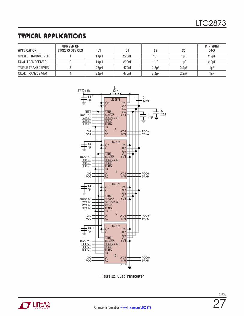
applicaTions inForMaTionPowering Multiple Devices
Multiple LTC2873 devices can be powered using the boost regulator from only one of the devices, requiring only one inductor (L1) and charge pump cap (C1). Since the RS232 drivers provide the primary load to the circuit, the following guidelines apply:
1. No more than four RS232 drivers can be supplied from a single device.
2. If more than two RS232 drivers are being supplied from a single device, then the inductor, L1, must be increased to 22µH and the charge pump cap, C1, must be increased to 470nH, and VDD and VEE bypass caps must be increased to 2.2µF.
3. Ground the SW pin on devices with inactive boost converters.
4. Connect CAP pins together for all devices.
5. Connect VEE pins together for all devices.
6. Connect VDD pins together for all devices.
Figures 32 shows an example of how to connect four devices.
Inductor Selection
A 10µH or 22μH (±20%) inductor with a saturation current (ISAT) rating of at least 220mA and a DCR (copper wire resistance) of less than 1.3Ω is required. Some very small inductors meeting these requirements are listed in Table 1.
Capacitor Selection
The small size of ceramic capacitors makes them ideal for the LTC2873. Use X5R or X7R dielectric types; their
ESR is low and they retain their capacitance over relatively wide voltage and temperature ranges. Use a voltage rating of at least 10V.
Running with External VDD and VEE Supplies
The inductor and charge pump cap, C1, can be omitted only if VDD and VEE are externally supplied. Bypass caps on VDD and VEE must remain in place. In this circumstance, ground the SW pin and float the CAP pin. External supplies must not exceed the absolute maximum levels of ±7.5V. Ideal supply levels are 7.2V and –6.5V as these are each just wider than the regulation points of 7.0V and –6.3V so the internal feedback is satisfied and the switching stops. Lower voltages can be used even at –6V and +6V but the internal boost regulator will be switching. This may cause some switching noise but will not harm the part. VDD and VEE supplies must be present for proper operation in RS232 mode and in RS485 mode when the termination is enabled. It is okay to run the LTC2873 in RS485 mode with internal termination disabled (TE485 high), when VDD and VEE are not present or fully settled.
Inrush Current and Supply Overshoot Precaution
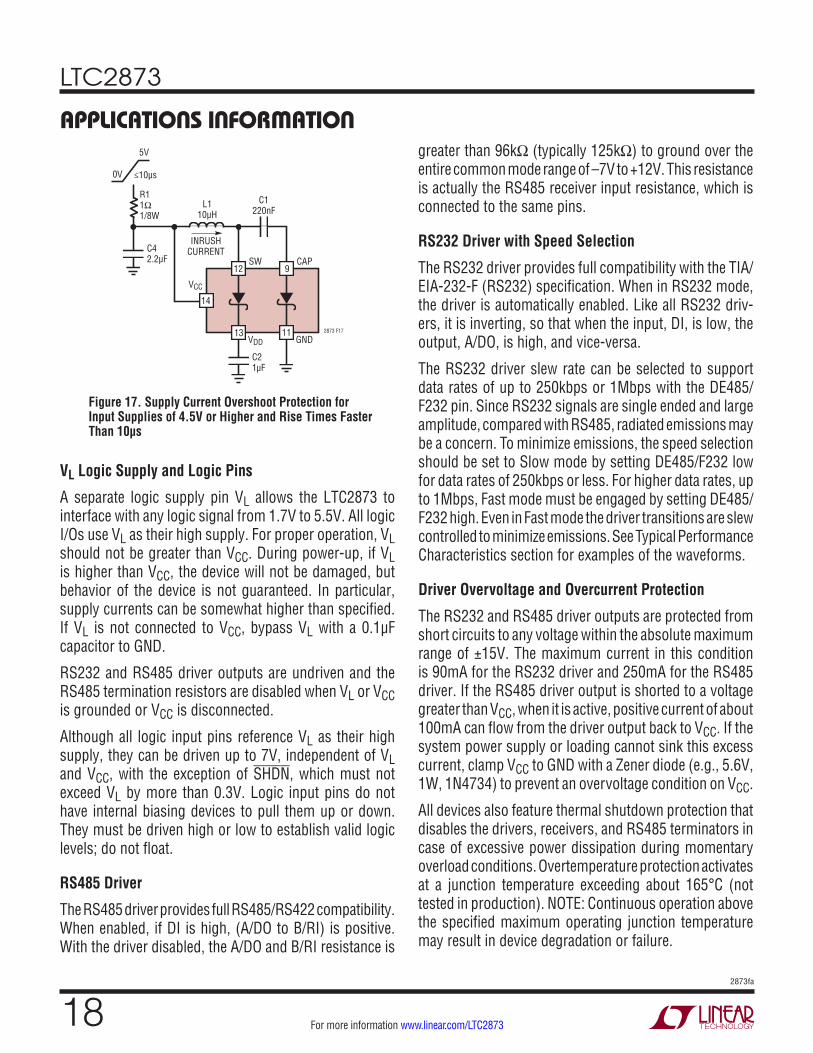
In certain applications, fast supply slew rates are generated when power is connected. If the VCC voltage is greater than 4.5V and its rise time is faster than 10µs, the pins VDD and SW can exceed their absolute maximum values during start-up. When supply voltage is applied to VCC, the voltage difference between VCC and VDD generates inrush current flowing through inductor L1 and capacitors C1 and C2. The peak inrush current must not exceed 2A. To avoid this condition, add a 1Ω resistor as shown in Figure 17. This precaution is not relevant for supply voltages below 4.5V or rise times longer than 10µs.
Table 1. Recommended Inductors
PART NUMBER L (μH) ISAT (mA) MAX DCR (Ω) SIZE (mm) MANUFACTURER
74479888310 10 250 0.5 2.5 × 2 × 1 Wurth Elektronik
CBC2016T100K (or M) 10 380 1.07 2 × 1.6 × 1.6Taiyo Yuden www.t-yuden.comCBC2518T220K (or M) 22 320 1.0 2.5 × 1.8 × 1.8
BRC2016T220K (or M) 22 310 1.3 2 × 1.6 × 1.6
LQH32CN220K53 22 250 0.92 3.2 × 2.5 × 1.6 Murata www.murata.com
LTC2873
182873fa
For more information www.linear.com/LTC2873
applicaTions inForMaTion
Figure 17. Supply Current Overshoot Protection for Input Supplies of 4.5V or Higher and Rise Times Faster Than 10μs
VL Logic Supply and Logic Pins
A separate logic supply pin VL allows the LTC2873 to interface with any logic signal from 1.7V to 5.5V. All logic I/Os use VL as their high supply. For proper operation, VL should not be greater than VCC. During power-up, if VL is higher than VCC, the device will not be damaged, but behavior of the device is not guaranteed. In particular, supply currents can be somewhat higher than specified. If VL is not connected to VCC, bypass VL with a 0.1µF capacitor to GND.
RS232 and RS485 driver outputs are undriven and the RS485 termination resistors are disabled when VL or VCC is grounded or VCC is disconnected.
Although all logic input pins reference VL as their high supply, they can be driven up to 7V, independent of VL and VCC, with the exception of SHDN, which must not exceed VL by more than 0.3V. Logic input pins do not have internal biasing devices to pull them up or down. They must be driven high or low to establish valid logic levels; do not float.
RS485 Driver
The RS485 driver provides full RS485/RS422 compatibility. When enabled, if DI is high, (A/DO to B/RI) is positive. With the driver disabled, the A/DO and B/RI resistance is
2873 F17
0V
5V
≤10µs
C1220nF
L110µH
INRUSHCURRENTC4
2.2µF
R11Ω1/8W
VCC
VDD GND
SW CAP
C21µF
14
12 9
13 11
greater than 96kΩ (typically 125kΩ) to ground over the entire common mode range of –7V to +12V. This resistance is actually the RS485 receiver input resistance, which is connected to the same pins.
RS232 Driver with Speed Selection
The RS232 driver provides full compatibility with the TIA/EIA-232-F (RS232) specification. When in RS232 mode, the driver is automatically enabled. Like all RS232 driv-ers, it is inverting, so that when the input, DI, is low, the output, A/DO, is high, and vice-versa.
The RS232 driver slew rate can be selected to support data rates of up to 250kbps or 1Mbps with the DE485/F232 pin. Since RS232 signals are single ended and large amplitude, compared with RS485, radiated emissions may be a concern. To minimize emissions, the speed selection should be set to Slow mode by setting DE485/F232 low for data rates of 250kbps or less. For higher data rates, up to 1Mbps, Fast mode must be engaged by setting DE485/F232 high. Even in Fast mode the driver transitions are slew controlled to minimize emissions. See Typical Performance Characteristics section for examples of the waveforms.
Driver Overvoltage and Overcurrent Protection
The RS232 and RS485 driver outputs are protected from short circuits to any voltage within the absolute maximum range of ±15V. The maximum current in this condition is 90mA for the RS232 driver and 250mA for the RS485 driver. If the RS485 driver output is shorted to a voltage greater than VCC, when it is active, positive current of about 100mA can flow from the driver output back to VCC. If the system power supply or loading cannot sink this excess current, clamp VCC to GND with a Zener diode (e.g., 5.6V, 1W, 1N4734) to prevent an overvoltage condition on VCC.
All devices also feature thermal shutdown protection that disables the drivers, receivers, and RS485 terminators in case of excessive power dissipation during momentary overload conditions. Overtemperature protection activates at a junction temperature exceeding about 165°C (not tested in production). NOTE: Continuous operation above the specified maximum operating junction temperature may result in device degradation or failure.
LTC2873
192873fa
For more information www.linear.com/LTC2873
Figure 18. RS485 Receiver Input Threshold Characteristics with Typical Values Shown
2873 F18
–110mV –70mV 0V
RA
+110mVA/DO TO B/RI
RISING THRESHOLDSHIFTS IF SIGNAL ISIN WINDOW > ~1.3µs
TO SUPPORTFAILSAFE
Typical applicaTionsRS485 Balanced Receiver with Full Failsafe Operation
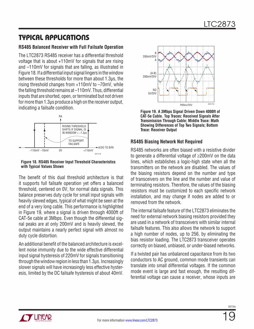
The LTC2873 RS485 receiver has a differential threshold voltage that is about +110mV for signals that are rising and –110mV for signals that are falling, as illustrated in Figure 18. If a differential input signal lingers in the window between these thresholds for more than about 1.3µs, the rising threshold changes from +110mV to –70mV, while the falling threshold remains at –110mV. Thus, differential inputs that are shorted, open, or terminated but not driven for more than 1.3µs produce a high on the receiver output, indicating a failsafe condition.
(A-B)200mV/DIV
B200mV/DIV
A
RO5V/DIV
2873 F19200ns/DIV
Figure 19. A 3Mbps Signal Driven Down 4000ft of CAT-5e Cable. Top Traces: Received Signals After Transmission Through Cable; Middle Trace: Math Showing Differences of Top Two Signals; Bottom Trace: Receiver Output
The benefit of this dual threshold architecture is that it supports full failsafe operation yet offers a balanced threshold, centered on 0V, for normal data signals. This balance preserves duty cycle for small input signals with heavily slewed edges, typical of what might be seen at the end of a very long cable. This performance is highlighted in Figure 19, where a signal is driven through 4000ft of CAT-5e cable at 3Mbps. Even though the differential sig-nal peaks are at only 200mV and is heavily slewed, the output maintains a nearly perfect signal with almost no duty cycle distortion.
An additional benefit of the balanced architecture is excel-lent noise immunity due to the wide effective differential input signal hysteresis of 220mV for signals transitioning through the window region in less than 1.3µs. Increasingly slower signals will have increasingly less effective hyster-esis, limited by the DC failsafe hysteresis of about 40mV.
RS485 Biasing Network Not Required
RS485 networks are often biased with a resistive divider to generate a differential voltage of ≥200mV on the data lines, which establishes a logic-high state when all the transmitters on the network are disabled. The values of the biasing resistors depend on the number and type of transceivers on the line and the number and value of terminating resistors. Therefore, the values of the biasing resistors must be customized to each specific network installation, and may change if nodes are added to or removed from the network.
The internal failsafe feature of the LTC2873 eliminates the need for external network biasing resistors provided they are used in a network of transceivers with similar internal failsafe features. This also allows the network to support a high number of nodes, up to 256, by eliminating the bias resistor loading. The LTC2873 transceiver operates correctly on biased, unbiased, or under-biased networks.
If a twisted pair has unbalanced capacitance from its two conductors to AC ground, common mode transients can translate into small differential voltages. If the common mode event is large and fast enough, the resulting dif-ferential voltage can cause a receiver, whose inputs are
LTC2873
202873fa
For more information www.linear.com/LTC2873
Figure 20. Equivalent RS485 Receiver Input Resistance Into A/DO and B/RI
2873 F20
A/DO
B/RI
TE485
60Ω
60Ω
125k
125k
undriven, to change state momentarily. In these extreme conditions, high quality shielded cable is recommended. If necessary, biasing resistors can be used on the bus to pull the resting signal farther from the receivers failsafe threshold.
Receiver Outputs
The RS232 and RS485 receiver outputs are internally driven high (to VL) or low (to GND) with no external pull up needed. When the receivers are disabled the output pin becomes Hi-Z with leakage of less than ±5µA for voltages within the VL supply range.
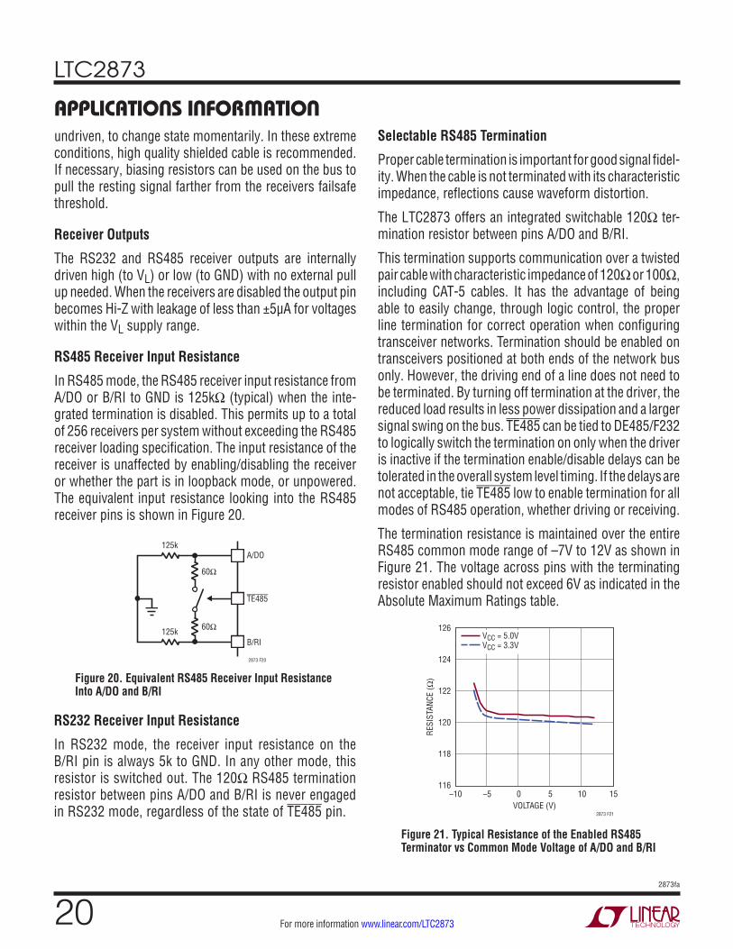
RS485 Receiver Input Resistance
In RS485 mode, the RS485 receiver input resistance from A/DO or B/RI to GND is 125kΩ (typical) when the inte-grated termination is disabled. This permits up to a total of 256 receivers per system without exceeding the RS485 receiver loading specification. The input resistance of the receiver is unaffected by enabling/disabling the receiver or whether the part is in loopback mode, or unpowered. The equivalent input resistance looking into the RS485 receiver pins is shown in Figure 20.
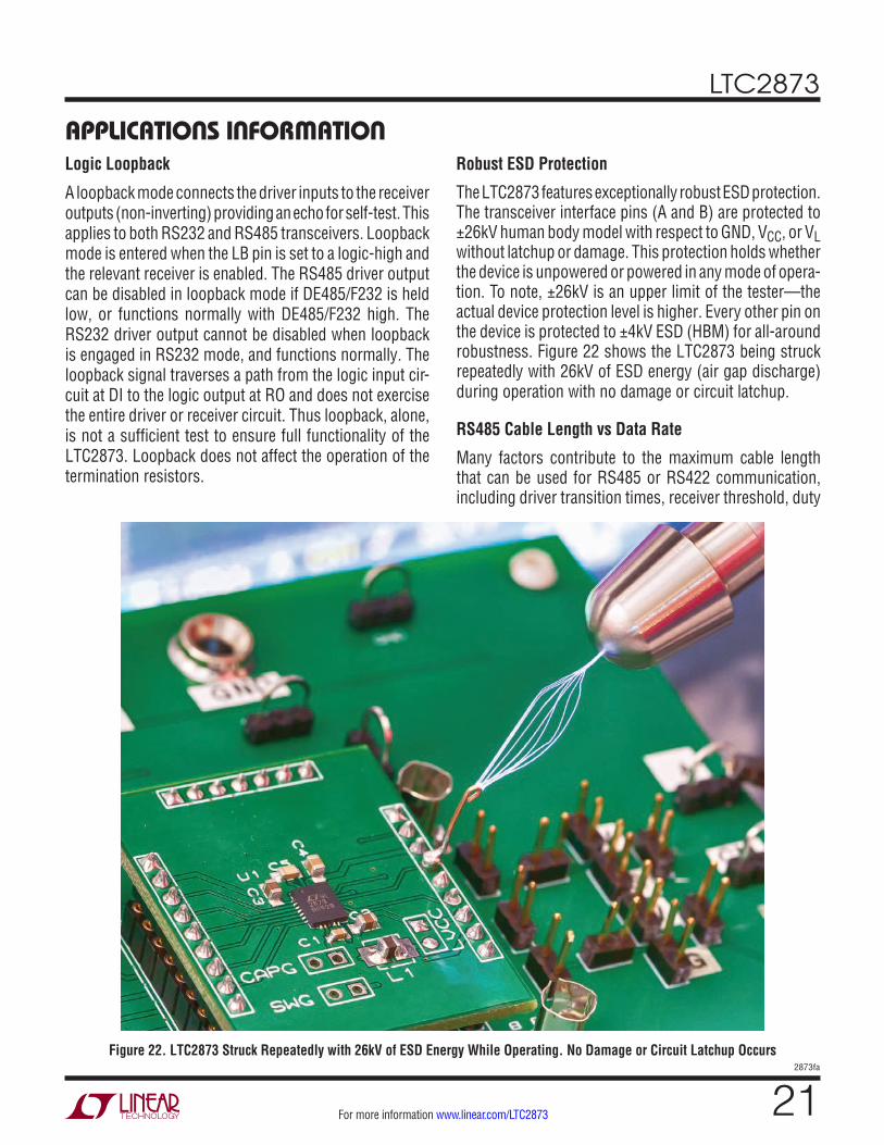
Figure 21. Typical Resistance of the Enabled RS485 Terminator vs Common Mode Voltage of A/DO and B/RI
VOLTAGE (V)–10
RESI
STAN
CE (Ω
)
126
124
122
118
120
11610–5
2873 F21
1550
VCC = 5.0VVCC = 3.3V
applicaTions inForMaTionSelectable RS485 Termination
Proper cable termination is important for good signal fidel-ity. When the cable is not terminated with its characteristic impedance, reflections cause waveform distortion.
The LTC2873 offers an integrated switchable 120Ω ter-mination resistor between pins A/DO and B/RI.
This termination supports communication over a twisted pair cable with characteristic impedance of 120Ω or 100Ω, including CAT-5 cables. It has the advantage of being able to easily change, through logic control, the proper line termination for correct operation when configuring transceiver networks. Termination should be enabled on transceivers positioned at both ends of the network bus only. However, the driving end of a line does not need to be terminated. By turning off termination at the driver, the reduced load results in less power dissipation and a larger signal swing on the bus. TE485 can be tied to DE485/F232 to logically switch the termination on only when the driver is inactive if the termination enable/disable delays can be tolerated in the overall system level timing. If the delays are not acceptable, tie TE485 low to enable termination for all modes of RS485 operation, whether driving or receiving.
The termination resistance is maintained over the entire RS485 common mode range of –7V to 12V as shown in Figure 21. The voltage across pins with the terminating resistor enabled should not exceed 6V as indicated in the Absolute Maximum Ratings table.
RS232 Receiver Input Resistance
In RS232 mode, the receiver input resistance on the B/RI pin is always 5k to GND. In any other mode, this resistor is switched out. The 120Ω RS485 termination resistor between pins A/DO and B/RI is never engaged in RS232 mode, regardless of the state of TE485 pin.
LTC2873
212873fa
For more information www.linear.com/LTC2873
applicaTions inForMaTionLogic Loopback
A loopback mode connects the driver inputs to the receiver outputs (non-inverting) providing an echo for self-test. This applies to both RS232 and RS485 transceivers. Loopback mode is entered when the LB pin is set to a logic-high and the relevant receiver is enabled. The RS485 driver output can be disabled in loopback mode if DE485/F232 is held low, or functions normally with DE485/F232 high. The RS232 driver output cannot be disabled when loopback is engaged in RS232 mode, and functions normally. The loopback signal traverses a path from the logic input cir-cuit at DI to the logic output at RO and does not exercise the entire driver or receiver circuit. Thus loopback, alone, is not a sufficient test to ensure full functionality of the LTC2873. Loopback does not affect the operation of the termination resistors.
Robust ESD Protection
The LTC2873 features exceptionally robust ESD protection. The transceiver interface pins (A and B) are protected to ±26kV human body model with respect to GND, VCC, or VL without latchup or damage. This protection holds whether the device is unpowered or powered in any mode of opera-tion. To note, ±26kV is an upper limit of the tester—the actual device protection level is higher. Every other pin on the device is protected to ±4kV ESD (HBM) for all-around robustness. Figure 22 shows the LTC2873 being struck repeatedly with 26kV of ESD energy (air gap discharge) during operation with no damage or circuit latchup.
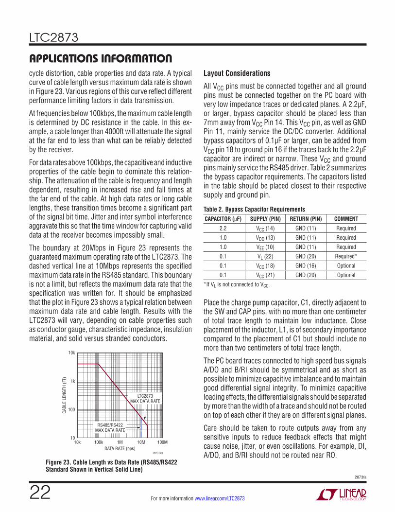
RS485 Cable Length vs Data Rate
Many factors contribute to the maximum cable length that can be used for RS485 or RS422 communication, including driver transition times, receiver threshold, duty
Figure 22. LTC2873 Struck Repeatedly with 26kV of ESD Energy While Operating. No Damage or Circuit Latchup Occurs
LTC2873
222873fa
For more information www.linear.com/LTC2873
Figure 23. Cable Length vs Data Rate (RS485/RS422 Standard Shown in Vertical Solid Line)
DATA RATE (bps)
CABL
E LE
NGTH
(FT)
2873 F23
10k
1k
100
1010k 10M 100M1M100k
LTC2873MAX DATA RATE
RS485/RS422MAX DATA RATE
cycle distortion, cable properties and data rate. A typical curve of cable length versus maximum data rate is shown in Figure 23. Various regions of this curve reflect different performance limiting factors in data transmission.
At frequencies below 100kbps, the maximum cable length is determined by DC resistance in the cable. In this ex-ample, a cable longer than 4000ft will attenuate the signal at the far end to less than what can be reliably detected by the receiver.
For data rates above 100kbps, the capacitive and inductive properties of the cable begin to dominate this relation-ship. The attenuation of the cable is frequency and length dependent, resulting in increased rise and fall times at the far end of the cable. At high data rates or long cable lengths, these transition times become a significant part of the signal bit time. Jitter and inter symbol interference aggravate this so that the time window for capturing valid data at the receiver becomes impossibly small.
The boundary at 20Mbps in Figure 23 represents the guaranteed maximum operating rate of the LTC2873. The dashed vertical line at 10Mbps represents the specified maximum data rate in the RS485 standard. This boundary is not a limit, but reflects the maximum data rate that the specification was written for. It should be emphasized that the plot in Figure 23 shows a typical relation between maximum data rate and cable length. Results with the LTC2873 will vary, depending on cable properties such as conductor gauge, characteristic impedance, insulation material, and solid versus stranded conductors.
applicaTions inForMaTionLayout Considerations
All VCC pins must be connected together and all ground pins must be connected together on the PC board with very low impedance traces or dedicated planes. A 2.2µF, or larger, bypass capacitor should be placed less than 7mm away from VCC Pin 14. This VCC pin, as well as GND Pin 11, mainly service the DC/DC converter. Additional bypass capacitors of 0.1µF or larger, can be added from VCC pin 18 to ground pin 16 if the traces back to the 2.2µF capacitor are indirect or narrow. These VCC and ground pins mainly service the RS485 driver. Table 2 summarizes the bypass capacitor requirements. The capacitors listed in the table should be placed closest to their respective supply and ground pin.
Table 2. Bypass Capacitor RequirementsCAPACITOR (µF) SUPPLY (PIN) RETURN (PIN) COMMENT
2.2 VCC (14) GND (11) Required
1.0 VDD (13) GND (11) Required
1.0 VEE (10) GND (11) Required
0.1 VL (22) GND (20) Required*
0.1 VCC (18) GND (16) Optional
0.1 VCC (21) GND (20) Optional
*If VL is not connected to VCC.
Place the charge pump capacitor, C1, directly adjacent to the SW and CAP pins, with no more than one centimeter of total trace length to maintain low inductance. Close placement of the inductor, L1, is of secondary importance compared to the placement of C1 but should include no more than two centimeters of total trace length.
The PC board traces connected to high speed bus signals A/DO and B/RI should be symmetrical and as short as possible to minimize capacitive imbalance and to maintain good differential signal integrity. To minimize capacitive loading effects, the differential signals should be separated by more than the width of a trace and should not be routed on top of each other if they are on different signal planes.
Care should be taken to route outputs away from any sensitive inputs to reduce feedback effects that might cause noise, jitter, or even oscillations. For example, DI, A/DO, and B/RI should not be routed near RO.

LTC2873
232873fa
For more information www.linear.com/LTC2873
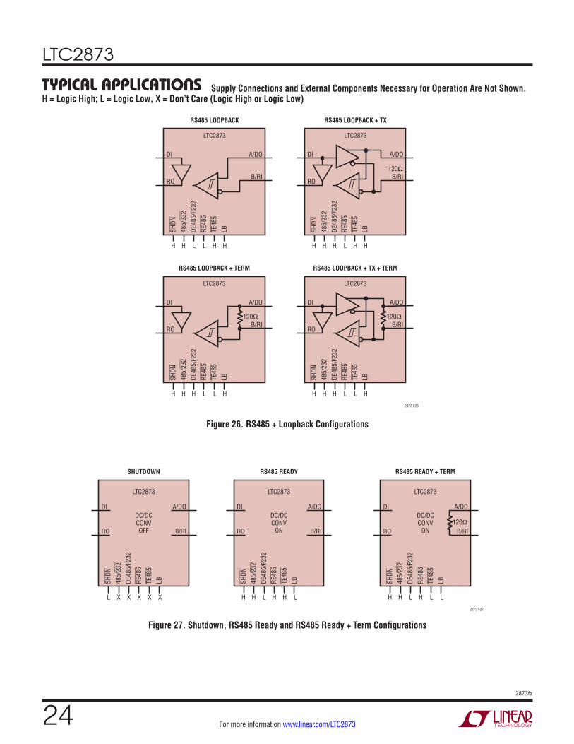
Typical applicaTions Supply Connections and External Components Necessary for Operation Are Not Shown. H = Logic High; L = Logic Low, X = Don’t Care (Logic High or Logic Low)
Figure 25. RS485 Configurations
2873 F25
LTC2873
RS485 TX + RX + TERM
A/DO
B/RI
DI
RO
SHDN
485/
232
RE48
5
TE48
5
DE48
5/F2
32
LB
H H H L L L
LTC2873
RS485 TX + TERM
A/DO
B/RI
DI
RO
SHDN
485/
232
RE48
5
TE48
5
DE48
5/F2
32
LB
H H H H L L
LTC2873
RS485 RX + TERM
A/DO
B/RI
DI
RO
SHDN
485/
232
RE48
5
TE48
5
DE48
5/F2
32
LB
H H L L L L
LTC2873
RS485 TX + RX
A/DO
B/RI
DI
RO
SHDN
485/
232
RE48
5
TE48
5
DE48
5/F2
32
LB
H H H L H L
LTC2873
RS485 TX
A/DO
B/RI
DI
RO
SHDN
485/
232
RE48
5
TE48
5
DE48
5/F2
32
LB
H H H H H L
LTC2873
RS485 RX
A/DO
B/RI
DI
RO
SHDN
485/
232
RE48
5
TE48
5
DE48
5/F2
32
LB
H H H L H L
120Ω 120Ω120Ω
Figure 24. RS232 Configurations
2873 F24
5k
LTC2873
RS232 SLOW
A/DO
B/RI
DI
RO
SHDN
485/
232
RE48
5
TE48
5
DE48
5/F2
32
LB
H L L X X L
5k
LTC2873
RS232 FAST
A/DO
B/RI
DI
RO
SHDN
485/
232
RE48
5
TE48
5
DE48
5/F2
32
LB
H L H X X L
5k
LTC2873
RS232 + LOOPBACK
A/DO
B/RI
DI
RO
SHDN
485/
232
RE48
5
TE48
5
DE48
5/F2
32
LB
H L X X X H
LTC2873
242873fa
For more information www.linear.com/LTC2873
Figure 26. RS485 + Loopback Configurations
Figure 27. Shutdown, RS485 Ready and RS485 Ready + Term Configurations
Typical applicaTions Supply Connections and External Components Necessary for Operation Are Not Shown. H = Logic High; L = Logic Low, X = Don’t Care (Logic High or Logic Low)
2873 F26
LTC2873
RS485 LOOPBACK + TX + TERM
A/DO
B/RI
DI
RO
SHDN
485/
232
RE48
5
TE48
5
DE48
5/F2
32
LB
H H H L L H
120Ω
LTC2873
RS485 LOOPBACK + TX
A/DO
B/RI
DI
RO
SHDN
485/
232
RE48
5
TE48
5
DE48
5/F2
32
LB
H H H L H H
120Ω
LTC2873
RS485 LOOPBACK + TERM
SHDN
485/
232
RE48
5
TE48
5
DE48
5/F2
32
LB
H H H L L H
120Ω
LTC2873
RS485 LOOPBACK
A/DO
B/RI
DI
ROSH
DN
485/
232
RE48
5
TE48
5
DE48
5/F2
32
LB
H H L L H H
A/DO
B/RI
DI
RO
2873 F27
LTC2873
DC/DCCONVOFF
SHUTDOWN
A/DO
B/RI
DI
RO
SHDN
485/
232
RE48
5
TE48
5
DE48
5/F2
32
LB
L X X X X X
LTC2873
DC/DCCONV
ON
A/DO
B/RI
DI
RO
SHDN
485/
232
RE48
5
TE48
5
DE48
5/F2
32
LB
H H L H H L
RS485 READY
LTC2873
DC/DCCONV
ON
A/DO
B/RI
DI
RO
SHDN
485/
232
RE48
5
TE48
5
DE48
5/F2
32
LB
H H L H L L
RS485 READY + TERM
120Ω
LTC2873
252873fa
For more information www.linear.com/LTC2873
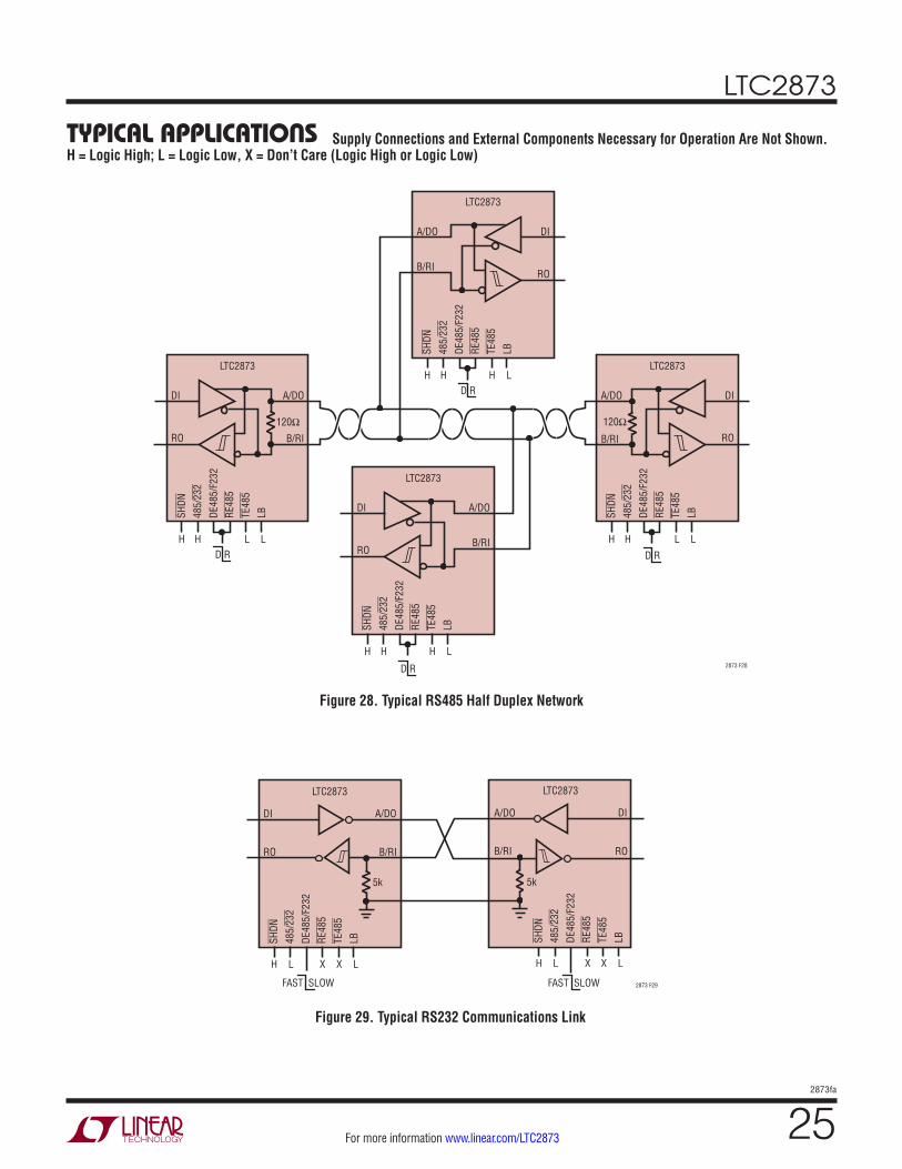
Figure 28. Typical RS485 Half Duplex Network
Figure 29. Typical RS232 Communications Link
Typical applicaTions Supply Connections and External Components Necessary for Operation Are Not Shown. H = Logic High; L = Logic Low, X = Don’t Care (Logic High or Logic Low)
2873 F28
LTC2873
DI
RO
A/DO
B/RI
SHDN
485/
232
RE48
5
TE48
5
DE48
5/F2
32
LB
H H L L
120Ω
LTC2873
A/DO
B/RI
DI
RO
SHDN
485/
232
RE48
5
TE48
5
DE48
5/F2
32
LB
H H L L
120Ω
LTC2873
A/DO
B/RI
DI
RO
SHDN
485/
232
RE48
5
TE48
5
DE48
5/F2
32
LB
H H H L
LTC2873
DI
RO
A/DO
B/RI
SHDN
485/
232
RE48
5
TE48
5
DE48
5/F2
32
LB
H H H L
D R
D RD R
D R
H L XX L
2873 F29
5k
LTC2873
A/DO
B/RI
DI
RO
SHDN
485/
232
RE48
5
TE48
5
DE48
5/F2
32
LB
H L XX L
5k
LTC2873
DI
RO
A/DO
B/RI
SHDN
485/
232
RE48
5
TE48
5
DE48
5/F2
32
LB
FAST SLOWFAST SLOW
LTC2873
262873fa
For more information www.linear.com/LTC2873
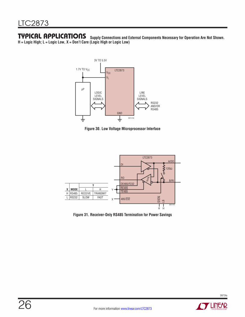
Figure 30. Low Voltage Microprocessor Interface
Figure 31. Receiver-Only RS485 Termination for Power Savings
Typical applicaTions Supply Connections and External Components Necessary for Operation Are Not Shown. H = Logic High; L = Logic Low, X = Don’t Care (Logic High or Logic Low)
2873 F30
3V TO 5.5V
1.7V TO VCC
µP
LTC2873
LOGICLEVEL
SIGNALS
LINELEVEL
SIGNALSRS232AND/ORRS485
VCC
VL
GND
2873 F31
120ΩDI
RO
485/232
RE485TE485
DE485/F232
A/DO
B/RI
LTC2873SH
DN
LB
H H
Y X MODE L H H RS485 RECEIVE TRANSMIT L RS232 SLOW FAST
Y
X
LTC2873
272873fa
For more information www.linear.com/LTC2873
Typical applicaTions
APPLICATIONNUMBER OF
LTC2873 DEVICES L1 C1 C2 C3MINIMUM
C4-X
SINGLE TRANSCEIVER 1 10µH 220nF 1µF 1µF 2.2µF
DUAL TRANSCEIVER 2 10µH 220nF 1µF 1µF 2.2µF
TRIPLE TRANSCEIVER 3 22µH 470nF 2.2µF 2.2µF 1µF
QUAD TRANSCEIVER 4 22µH 470nF 2.2µF 2.2µF 1µF
Figure 32. Quad Transceiver
DI-ARO-A
VCCVL
SHDN485/232
LBTE485
DIRO
DE485/F232RE485
SHDN485/232-A
LBTE485-A
DX485-ARX485-A
SWCAPVDDVEE
GND
A/DOB/RI
A/DO-AB/RI-A
L122µH
C1470nF
C4-A1µF LTC2873
2873 F32
LTC2873
LTC2873
LTC2873
A
DI-BRO-B
VCCVL
SHDN485/232
LBTE485
DIRO
DE485/F232RE485
485/232-B
TE485-B
DX485-BRX485-B
SWCAPVDDVEE
GND
A/DOB/RI
A/DO-BB/RI-B
B
C4-B1µF
DI-CRO-C
VCCVL
SHDN485/232
LBTE485
DIRO
DE485/F232RE485
485/232-C
TE485-C
DX485-CRX485-C
SWCAPVDDVEE
GND
A/DOB/RI
A/DO-CB/RI-C
C
C4-C1µF
DI-DRO-D
VCCVL
SHDN485/232
LBTE485
DIRO
DE485/F232RE485
485/232-D
TE485-D
DX485-DRX485-D
SWCAPVDDVEE
GND
A/DOB/RI
A/DO-DB/RI-D
D
C4-D1µF
C32.2µF
C22.2µF
3V TO 5.5V
LTC2873
282873fa
For more information www.linear.com/LTC2873
package DescripTionPlease refer to http://www.linear.com/product/LTC2873#packaging/ for the most recent package drawings.
4.00 ±0.10(2 SIDES)
5.00 ±0.10(2 SIDES)
NOTE:1. DRAWING PROPOSED TO BE MADE A JEDEC PACKAGE OUTLINE MO-220 VARIATION (WXXX-X).2. DRAWING NOT TO SCALE3. ALL DIMENSIONS ARE IN MILLIMETERS4. DIMENSIONS OF EXPOSED PAD ON BOTTOM OF PACKAGE DO NOT INCLUDE MOLD FLASH. MOLD FLASH, IF PRESENT, SHALL NOT EXCEED 0.15mm ON ANY SIDE5. EXPOSED PAD SHALL BE SOLDER PLATED6. SHADED AREA IS ONLY A REFERENCE FOR PIN 1 LOCATION ON THE TOP AND BOTTOM OF PACKAGE
PIN 1TOP MARK(NOTE 6)
0.40 ±0.10
23 24
1
2
BOTTOM VIEW—EXPOSED PAD
0.75 ±0.05R = 0.115TYP
R = 0.05 TYP PIN 1 NOTCHR = 0.20 OR C = 0.35
0.25 ±0.05
0.50 BSC
0.200 REF
0.00 – 0.05
(UFD24) QFN 0506 REV A
RECOMMENDED SOLDER PAD PITCH AND DIMENSIONSAPPLY SOLDER MASK TO AREAS THAT ARE NOT SOLDERED
0.70 ±0.05
0.25 ±0.050.50 BSC
2.65 ±0.052.00 REF
3.00 REF4.10 ±0.055.50 ±0.05
3.10 ±0.05
4.50 ±0.05
PACKAGE OUTLINE
2.65 ±0.10
2.00 REF
3.00 REF3.65 ±0.10
3.65 ±0.05
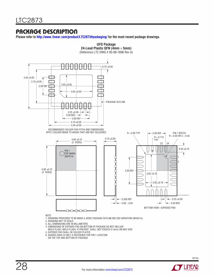
UFD Package24-Lead Plastic QFN (4mm × 5mm)
(Reference LTC DWG # 05-08-1696 Rev A)
LTC2873
292873fa
For more information www.linear.com/LTC2873
Information furnished by Linear Technology Corporation is believed to be accurate and reliable. However, no responsibility is assumed for its use. Linear Technology Corporation makes no representa-tion that the interconnection of its circuits as described herein will not infringe on existing patent rights.
revision hisToryREV DATE DESCRIPTION PAGE NUMBER
A 05/16 Applied Note 7 to tZLSR232, tZHSR232.Added Exposed Pad soldering requirement to VEE pin description.Corrected recommended Wurth inductor part number.
69
17
LTC2873
302873fa
For more information www.linear.com/LTC2873 LINEAR TECHNOLOGY CORPORATION 2016
LT 0516 REV A • PRINTED IN USALinear Technology Corporation1630 McCarthy Blvd., Milpitas, CA 95035-7417(408) 432-1900 FAX: (408) 434-0507 www.linear.com/LTC2873
relaTeD parTs
Typical applicaTion
PART NUMBER DESCRIPTION COMMENTS
LTC2870, LTC2871 RS232/RS485 Multiprotocol Transceiver with Integrated Termination
Two RS232 and One RS485 Transceivers. 3V to 5.5V Supply, Automatic Selection of Termination Resistors, Duplex Control, Logic Supply Pin, Up to ±26kV ESD
LTC2872 RS232/RS485 Dual Multiprotocol Transceiver with Integrated Termination
Four RS232 and Two RS485 Transceivers. 3V to 5.5V Supply, Automatic Selection of Termination Resistors, Duplex Control, Logic Supply Pin, ±15kV ESD
LTC1334 Single 5V RS232/RS485 Multiprotocol Transceiver Dual Port, Single 5V Supply, Configurable, ±10kV ESD
LTC1387 Single 5V RS232/RS485 Multiprotocol Transceiver Single Port, Configurable
LTC2801/LTC2802/ LTC2803/LTC2804
1.8V to 5.5V RS232 Single and Dual Transceivers Up to 1Mbps, ±10kV ESD, Logic Supply Pin, Tiny DFN Packages
LTC2854/LTC2855 3.3V 20Mbps RS485 Transceiver with Integrated Switchable Termination
3.3V Supply, Integrated, Switchable, 120Ω Termination Resistor, ±25kV ESD
LTC2859/LTC2861 20Mbps RS485 Transceiver with Integrated Switchable Termination
5V Supply, Integrated, Switchable, 120Ω Termination Resistor, ±15kV ESD
LTM®2881 Complete Isolated RS485/RS422 µModule® Transceiver + Power
20Mbps, 2500VRMS Isolation with Integrated DC/DC Converter, Integrated Switchable 120Ω Termination Resistor, ±15kV ESD
LTM2882 Dual Isolated RS232 µModule Transceiver + Power 1Mbps, 2500VRMS Isolation with Integrated DC/DC Converter, ±10kV ESD
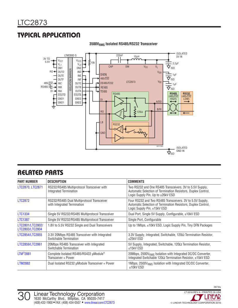
3500VRMS Isolated RS485/RS232 Transceiver
2873 TA02
120Ω
5k
1μF
ISOLATED5V IN220nF 10μH
2.2μF
ISO
ISO
VLCAP SW
SHDN
DI
RO
485/232
RE485TE485
DE485/F232
LB
GND
RS232
RS485
A/DO
B/RI
VDD
VEE
VCC
1μF
ISOLTC2873
ISOLATEDGND IN
3V TO5.5V
DI
RO
485/232RS485 D R
ISO
10k
RS232(485/232
LOW)
RS485(485/232
HIGH)
VCC2VL2
ON2INDINEINF
OUTCOUTBOUTA
EOUTAGND2GND2
VCC1VL1ON1OUTDOUTEOUTFINCINBINAEOUTDGND1GND1
LTM2892-S
ISOL
ATIO
N BA
RRIE
R