low-voltage motor driver ic - farnell … slvsab3h –may 2010–revised october 2013 low-voltage...
TRANSCRIPT
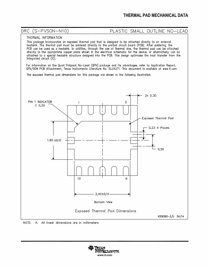
DRV8832
www.ti.com SLVSAB3H –MAY 2010–REVISED OCTOBER 2013
LOW-VOLTAGE MOTOR DRIVER ICCheck for Samples: DRV8832
1FEATURES2• H-Bridge Voltage-Controlled Motor Driver • Fault Output
– Drives DC Motor, One Winding of a Stepper • Thermally Enhanced Surface Mount PackagesMotor, or Other Actuators/Loads
APPLICATIONS– Efficient PWM Voltage Control for ConstantMotor Speed With Varying Supply Voltages • Battery-Powered:
– Low MOSFET On-Resistance: – PrintersHS + LS 450 mΩ – Toys
• 1-A Maximum DC/RMS or Peak Drive Current – Robotics• 2.75-V to 6.8-V Operating Supply Voltage – Cameras
Range – Phones• 300-nA (Typical) Sleep Mode Current • Small Actuators, Pumps, etc.• Reference Voltage Output• Current Limit Circuit
DESCRIPTIONThe DRV8832 provides an integrated motor driver solution for battery-powered toys, printers, and other low-voltage or battery-powered motion control applications. The device has one H-bridge driver, and can drive oneDC motor or one winding of a stepper motor, as well as other loads like solenoids. The output driver blockconsists of N-channel and P-channel power MOSFET’s configured as an H-bridge to drive the motor winding.
Provided with sufficient PCB heatsinking, the DRV8832 can supply up to 1-A of DC/RMS or peak output current.It operates on power supply voltages from 2.75 V to 6.8 V.
To maintain constant motor speed over varying battery voltages while maintaining long battery life, a PWMvoltage regulation method is provided. An input pin allows programming of the regulated voltage. A built-involtage reference output is also provided.
Internal protection functions are provided for over current protection, short circuit protection, under voltagelockout and overtemperature protection.
The DRV8832 also provides a current limit function to regulate the motor current during conditions like motorstartup or stall, as well as a fault output pin to signal a host processor of a fault condition.
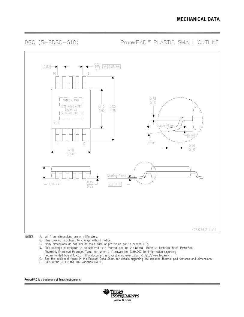
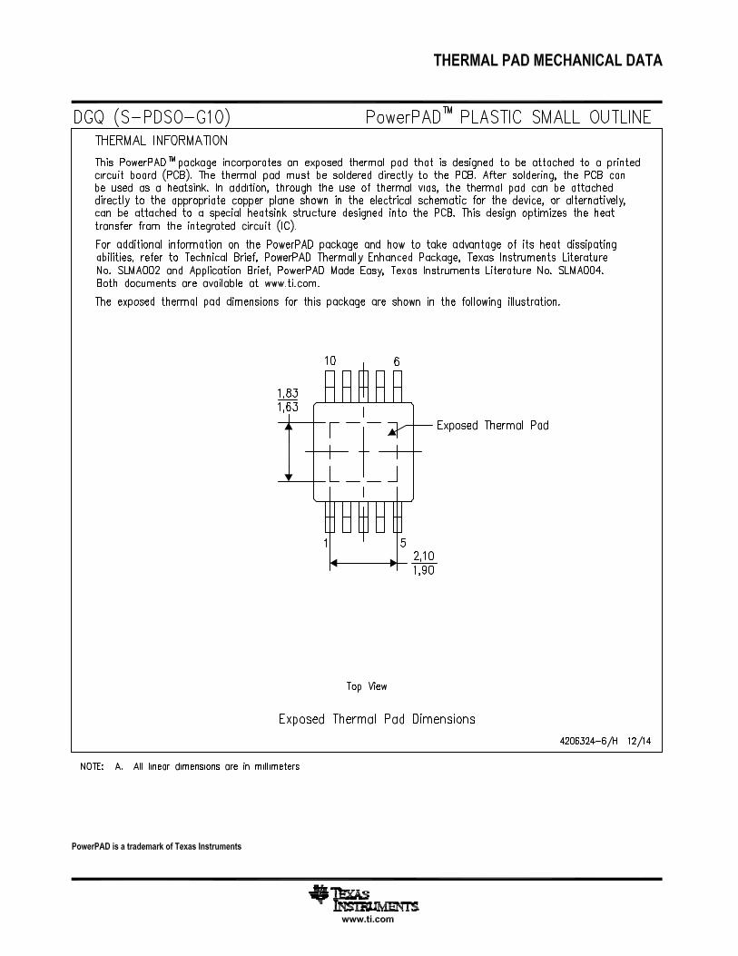
The DRV8832 is available in tiny 3-mm x 3-mm 10-pin MSOP and WSON packages with PowerPAD™ (Eco-friendly: RoHS & no Sb/Br).
ORDERING INFORMATION (1)
ORDERABLE PART TOP-SIDEPACKAGE (2)NUMBER MARKING
Reel of 2500 DRV8832DGQR 8832PowerPAD™ (MSOP) - DGQ
Tube of 80 DRV8832DGQ 8832Reel of 3000 DRV8832DRCR 8832
PowerPAD™ (WSON) - DRCReel of 250 DRV8832DRCT 8832
(1) For the most current packaging and ordering information, see the Package Option Addendum at the end of this document, or see the TIweb site at www.ti.com.
(2) Package drawings, thermal data, and symbolization are available at www.ti.com/packaging.
1
Please be aware that an important notice concerning availability, standard warranty, and use in critical applications ofTexas Instruments semiconductor products and disclaimers thereto appears at the end of this data sheet.
2PowerPAD is a trademark of Texas Instruments.PRODUCTION DATA information is current as of publication date. Copyright © 2010–2013, Texas Instruments IncorporatedProducts conform to specifications per the terms of the TexasInstruments standard warranty. Production processing does notnecessarily include testing of all parameters.
Over-
Temp
OUT1
OUT2
GND
IN1
VREF
VSET
VCCVCC
VCC
Battery
DCM
Gate
Drive
Integ.
Comp
+
-
Logic
Ref
Osc
OCP
VCC
Gate
Drive
OCP
IN2
Current
Sense
FAULTn
ISENSE
DRV8832
SLVSAB3H –MAY 2010–REVISED OCTOBER 2013 www.ti.com
This integrated circuit can be damaged by ESD. Texas Instruments recommends that all integrated circuits be handled withappropriate precautions. Failure to observe proper handling and installation procedures can cause damage.
ESD damage can range from subtle performance degradation to complete device failure. Precision integrated circuits may be moresusceptible to damage because very small parametric changes could cause the device not to meet its published specifications.
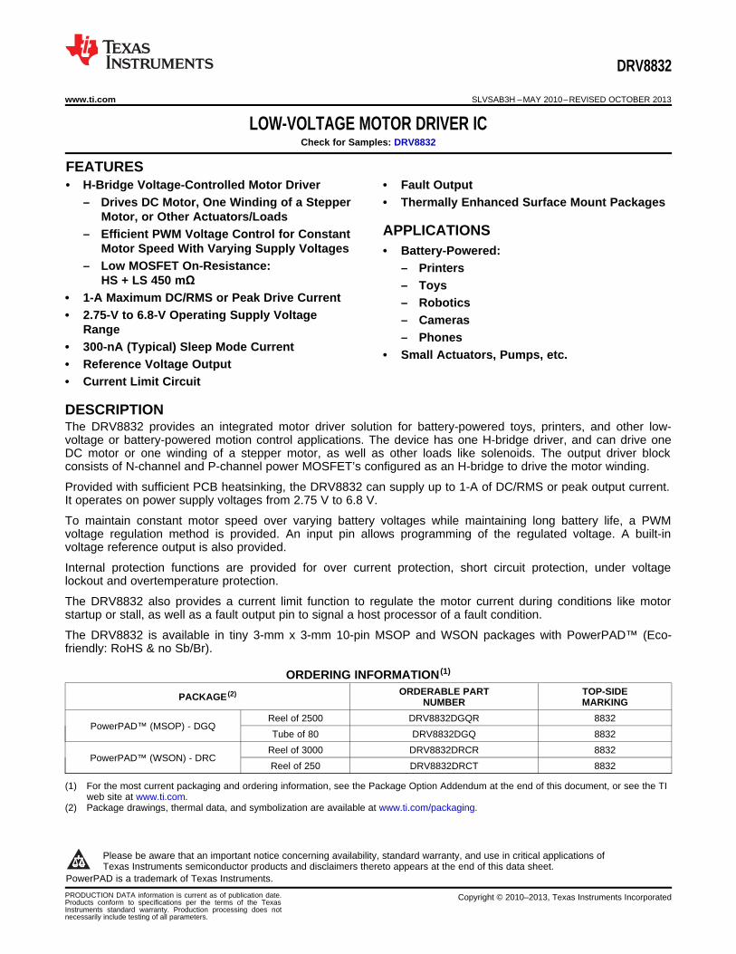
DEVICE INFORMATIONFunctional Block Diagram
2 Submit Documentation Feedback Copyright © 2010–2013, Texas Instruments Incorporated
Product Folder Links: DRV8832

1
2
3
4
10
9
8
7
GND
(PPAD)
IN2IN1VREFVSET
OUT1VCC
ISENSE
OUT2
5 6 FAULTnGND
DGQ OR DRC PACKAGE
(TOP VIEW)
DRV8832
www.ti.com SLVSAB3H –MAY 2010–REVISED OCTOBER 2013
Table 1. TERMINAL FUNCTIONSEXTERNAL COMPONENTSNAME PIN I/O (1) DESCRIPTION OR CONNECTIONS
GND 5 - Device groundBypass to GND with a 0.1-μF (minimum)VCC 4 - Device and motor supply ceramic capacitor.
IN1 9 I Bridge A input 1 Logic high sets OUT1 highIN2 10 I Bridge A input 2 Logic high sets OUT2 high
VREF 8 O Reference voltage output Reference voltage outputVSET 7 I Voltage set input Input voltage sets output regulation voltage
Open-drain output driven low if fault conditionFAULTn 6 OD Fault output presentOUT1 3 O Bridge output 1 Connect to motor windingOUT2 1 O Bridge output 2 Connect to motor winding
Connect current sense resistor to GND.ISENSE 2 IO Current sense resistor Resistor value sets current limit level.
(1) Directions: I = input, O = output, OZ = tri-state output, OD = open-drain output, IO = input/output
ABSOLUTE MAXIMUM RATINGS (1) (2)
VALUE UNITVCC Power supply voltage range –0.3 to 7 V
Input pin voltage range –0.5 to 7 VPeak motor drive output current (3) Internally limited AContinuous motor drive output current (3) 1 AContinuous total power dissipation See Dissipation Ratings table
TJ Operating virtual junction temperature range –40 to 150 °CTstg Storage temperature range –60 to 150 °C
(1) Stresses beyond those listed under absolute maximum ratings may cause permanent damage to the device. These are stress ratingsonly, and functional operation of the device at these or any other conditions beyond those indicated under recommended operatingconditions is not implied. Exposure to absolute–maximum–rated conditions for extended periods may affect device reliability.
(2) All voltage values are with respect to network ground terminal.(3) Power dissipation and thermal limits must be observed.
Copyright © 2010–2013, Texas Instruments Incorporated Submit Documentation Feedback 3
Product Folder Links: DRV8832

DRV8832
SLVSAB3H –MAY 2010–REVISED OCTOBER 2013 www.ti.com
THERMAL INFORMATIONDRV8832 DRV8832
THERMAL METRIC (1) DGQ DRC UNITS10 PINS 10 PINS
θJA Junction-to-ambient thermal resistance (2) 69.3 50.2θJCtop Junction-to-case (top) thermal resistance (3) 63.5 78.4θJB Junction-to-board thermal resistance (4) 51.6 18.8
°C/WψJT Junction-to-top characterization parameter (5) 1.5 1.1ψJB Junction-to-board characterization parameter (6) 23.2 17.9θJCbot Junction-to-case (bottom) thermal resistance (7) 9.5 5.1
(1) For more information about traditional and new thermal metrics, see the IC Package Thermal Metrics application report, SPRA953.(2) The junction-to-ambient thermal resistance under natural convection is obtained in a simulation on a JEDEC-standard, high-K board, as
specified in JESD51-7, in an environment described in JESD51-2a.(3) The junction-to-case (top) thermal resistance is obtained by simulating a cold plate test on the package top. No specific JEDEC-
standard test exists, but a close description can be found in the ANSI SEMI standard G30-88.(4) The junction-to-board thermal resistance is obtained by simulating in an environment with a ring cold plate fixture to control the PCB
temperature, as described in JESD51-8.(5) The junction-to-top characterization parameter, ψJT, estimates the junction temperature of a device in a real system and is extracted
from the simulation data for obtaining θJA, using a procedure described in JESD51-2a (sections 6 and 7).(6) The junction-to-board characterization parameter, ψJB, estimates the junction temperature of a device in a real system and is extracted
from the simulation data for obtaining θJA , using a procedure described in JESD51-2a (sections 6 and 7).(7) The junction-to-case (bottom) thermal resistance is obtained by simulating a cold plate test on the exposed (power) pad. No specific
JEDEC standard test exists, but a close description can be found in the ANSI SEMI standard G30-88.Spacer
RECOMMENDED OPERATING CONDITIONSover operating free-air temperature range (unless otherwise noted)
MIN NOM MAX UNITVCC Motor power supply voltage range 2.75 6.8 VIOUT Continuous or peak H-bridge output current (1) 0 1 A
(1) Power dissipation and thermal limits must be observed.
4 Submit Documentation Feedback Copyright © 2010–2013, Texas Instruments Incorporated
Product Folder Links: DRV8832
DRV8832
www.ti.com SLVSAB3H –MAY 2010–REVISED OCTOBER 2013
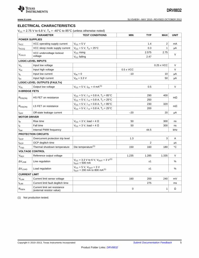
ELECTRICAL CHARACTERISTICSVCC = 2.75 V to 6.8 V, TA = -40°C to 85°C (unless otherwise noted)
PARAMETER TEST CONDITIONS MIN TYP MAX UNITPOWER SUPPLIESIVCC VCC operating supply current VCC = 5 V 1.4 2 mAIVCCQ VCC sleep mode supply current VCC = 5 V, TA = 25°C 0.3 1 μA
VCC rising 2.575 2.75VCC undervoltage lockoutVUVLO Vvoltage VCC falling 2.47LOGIC-LEVEL INPUTSVIL Input low voltage 0.25 x VCC VVIH Input high voltage 0.5 x VCC VIIL Input low current VIN = 0 -10 10 μAIIH Input high current VIN = 3.3 V 50 μALOGIC-LEVEL OUTPUTS (FAULTn)VOL Output low voltage VCC = 5 V, IOL = 4 mA (1) 0.5 VH-BRIDGE FETS
VCC = 5 V, I O = 0.8 A, TJ = 85°C 290 400RDS(ON) HS FET on resistance mΩ
VCC = 5 V, I O = 0.8 A, TJ = 25°C 250VCC = 5 V, I O = 0.8 A, TJ = 85°C 230 320
RDS(ON) LS FET on resistance mΩVCC = 5 V, I O = 0.8 A, TJ = 25°C 200
IOFF Off-state leakage current –20 20 μAMOTOR DRIVERtR Rise time VCC = 3 V, load = 4 Ω 50 300 nstF Fall time VCC = 3 V, load = 4 Ω 50 300 nsfSW Internal PWM frequency 44.5 kHzPROTECTION CIRCUITSIOCP Overcurrent protection trip level 1.3 3 AtOCP OCP deglitch time 2 μsTTSD Thermal shutdown temperature Die temperature (1) 150 160 180 °CVOLTAGE CONTROLVREF Reference output voltage 1.235 1.285 1.335 V
VCC = 3.3 V to 6 V, VOUT = 3 V (1)ΔVLINE Line regulation ±1 %IOUT = 500 mA
VCC = 5 V, VOUT = 3 VΔVLOAD Load regulation ±1 %IOUT = 200 mA to 800 mA (1)
CURRENT LIMITVILIM Current limit sense voltage 160 200 240 mVtILIM Current limit fault deglitch time 275 ms
Current limit set resistanceRISEN 0 1 Ω(external resistor value)
(1) Not production tested.
Copyright © 2010–2013, Texas Instruments Incorporated Submit Documentation Feedback 5
Product Folder Links: DRV8832

0%
10%
20%
30%
40%
50%
60%
70%
80%
90%
100%
0.5 1.5 2.5 3.5 4.5 5.5
V - VOUT
EF
FIC
EN
CY
Linear Regulator
DRV8832
50%
55%
60%
65%
70%
75%
80%
85%
90%
95%
100%
0.2 0.4 0.6 0.8
LOAD - A
EF
FIC
IEN
CY
DRV8832
SLVSAB3H –MAY 2010–REVISED OCTOBER 2013 www.ti.com
TYPICAL PERFORMANCE GRAPHSEFFICIENCY
vsLOAD CURRENT
(VIN = 5 V, VOUT = 3 V)
Figure 1.
EFFICIENCYvs
OUTPUT VOLTAGE(VIN = 5 V, IOUT = 500 mA)
Figure 2.
6 Submit Documentation Feedback Copyright © 2010–2013, Texas Instruments Incorporated
Product Folder Links: DRV8832

OUT1
OUT2
VCC
IN2 Pre-
drive
VCC
+
-
PWM
OCP
OCP
IN1
VSET
Integrator DIFF
COMP
DCM
/4
ISEN+
-COMP
REF
ITRIP
DRV8832
www.ti.com SLVSAB3H –MAY 2010–REVISED OCTOBER 2013
FUNCTIONAL DESCRIPTION
Power SupervisorThe DRV8832 is capable of entering a low-power sleep mode by bringing both of the INx control inputs logic low.The outputs will be disabled Hi-Z.
In order to exit the sleep mode, bring either or both of the INx inputs logic high. This will enable the H-bridges.When exiting the sleep mode, the FAULTn pin will pulse low.
PWM Motor DriverThe DRV8832 contains an H-bridge motor driver with PWM voltage-control circuitry with current limit circuitry. Ablock diagram of the motor control circuitry is shown below.
Figure 3. Motor Control Circuitry
Bridge ControlThe IN1 and IN2 control pins enable the H-bridge outputs. The following table shows the logic:
Table 2. H-Bridge LogicIN1 IN2 OUT1 OUT2 Function0 0 Z Z Sleep/Coast0 1 L H Reverse1 0 H L Forward1 1 H H Brake
When both inputs are low, the output drivers are disabled and the device is placed into a low-power sleep state.The current limit fault condition (if present) is also cleared. Note that when transitioning from either brake or sleepmode to forward or reverse, the voltage control PWM starts at zero duty cycle. The duty cycle slowly ramps up tothe commanded voltage. This can take up to 12 ms to go from sleep to 100% duty cycle. Because of this, high-speed PWM signals cannot be applied to the IN1 and IN2 pins. To control motor speed, use the VSET pin asdescribed below.
Copyright © 2010–2013, Texas Instruments Incorporated Submit Documentation Feedback 7
Product Folder Links: DRV8832
OUT1 OUT2
2
1
2
PWM on
PWM off
VCC
1Shown with
IN1=1, IN2=0
DRV8832
SLVSAB3H –MAY 2010–REVISED OCTOBER 2013 www.ti.com
Because of the sleep mode functionality described previously, when applying an external PWM to the DRV8832,hold one input logic high while applying a PWM signal to the other. If the logic input is held low instead, then thedevice will cycle in and out of sleep mode, causing the FAULTn pin to pulse low on every sleep mode exit.
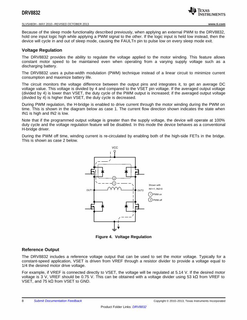
Voltage RegulationThe DRV8832 provides the ability to regulate the voltage applied to the motor winding. This feature allowsconstant motor speed to be maintained even when operating from a varying supply voltage such as adischarging battery.
The DRV8832 uses a pulse-width modulation (PWM) technique instead of a linear circuit to minimize currentconsumption and maximize battery life.
The circuit monitors the voltage difference between the output pins and integrates it, to get an average DCvoltage value. This voltage is divided by 4 and compared to the VSET pin voltage. If the averaged output voltage(divided by 4) is lower than VSET, the duty cycle of the PWM output is increased; if the averaged output voltage(divided by 4) is higher than VSET, the duty cycle is decreased.
During PWM regulation, the H-bridge is enabled to drive current through the motor winding during the PWM ontime. This is shown in the diagram below as case 1. The current flow direction shown indicates the state whenIN1 is high and IN2 is low.
Note that if the programmed output voltage is greater than the supply voltage, the device will operate at 100%duty cycle and the voltage regulation feature will be disabled. In this mode the device behaves as a conventionalH-bridge driver.
During the PWM off time, winding current is re-circulated by enabling both of the high-side FETs in the bridge.This is shown as case 2 below.
Figure 4. Voltage Regulation
Reference OutputThe DRV8832 includes a reference voltage output that can be used to set the motor voltage. Typically for aconstant-speed application, VSET is driven from VREF through a resistor divider to provide a voltage equal to1/4 the desired motor drive voltage.
For example, if VREF is connected directly to VSET, the voltage will be regulated at 5.14 V. If the desired motorvoltage is 3 V, VREF should be 0.75 V. This can be obtained with a voltage divider using 53 kΩ from VREF toVSET, and 75 kΩ from VSET to GND.
8 Submit Documentation Feedback Copyright © 2010–2013, Texas Instruments Incorporated
Product Folder Links: DRV8832
R =ISENSE
200 mV¾
ILIMIT
DRV8832
www.ti.com SLVSAB3H –MAY 2010–REVISED OCTOBER 2013
Current LimitA current limit circuit is provided to protect the system in the event of an overcurrent condition, such as whatwould be encountered if driving a DC motor at start-up or with an abnormal mechanical load (stall condition).
The motor current is sensed by monitoring the voltage across an external sense resistor. When the voltageexceeds a reference voltage of 200 mV for more than approximately 3 µs, the PWM duty cycle is reduced to limitthe current through the motor to this value. This current limit allows for starting the motor while controlling thecurrent.
If the current limit condition persists for some time, it is likely that a fault condition has been encountered, suchas the motor being run into a stop or a stalled condition. An overcurrent event must persist for approximately275 ms before the fault is registered. After approximately 275 ms, a fault signaled to the host by driving theFAULTn signal low. Operation of the motor driver will continue.
The current limit fault condition is cleared by taking both IN1 and IN2 low to disable the motor current, or byremoving and re-applying power to the device.
The resistor used to set the current limit must be less than 1 Ω. Its value may be calculated as follows:
(1)
Where:
RISENSE is the current sense resistor value.
ILIMIT is the desired current limit (in mA).
If the current limit feature is not needed, the ISENSE pin may be directly connected to ground.
Protection CircuitsThe DRV8832 is fully protected against undervoltage, overcurrent and overtemperature events.
Overcurrent Protection (OCP)An analog current limit circuit on each FET limits the current through the FET by removing the gate drive. If thisanalog current limit persists for longer than the OCP time, all FETs in the H-bridge will be disabled, and theFAULTn signal will be driven low. The device will remain disabled until VCC is removed and re-applied.
Overcurrent conditions are sensed independently on both high and low side devices. A short to ground, supply,or across the motor winding will all result in an overcurrent shutdown. Note that OCP is independent of thecurrent limit function, which is typically set to engage at a lower current level; the OCP function is intended toprevent damage to the device under abnormal (e.g., short-circuit) conditions.
Thermal Shutdown (TSD)If the die temperature exceeds safe limits, all FETs in the H-bridge will be disabled and the FAULTn signal will bedriven low. Once the die temperature has fallen to a safe level operation will automatically resume.
Undervoltage Lockout (UVLO)If at any time the voltage on the VCC pins falls below the undervoltage lockout threshold voltage, all circuitry inthe device will be disabled, the FAULTn signal will be driven low, and internal logic will be reset. Operation willresume when VCC rises above the UVLO threshold.
Copyright © 2010–2013, Texas Instruments Incorporated Submit Documentation Feedback 9
Product Folder Links: DRV8832
P = R (I )TOT DS(ON) OUT(RMS)22
· ·
DRV8832
SLVSAB3H –MAY 2010–REVISED OCTOBER 2013 www.ti.com
THERMAL INFORMATION
Thermal ProtectionThe DRV8832 has thermal shutdown (TSD) as described above. If the die temperature exceeds approximately160°C, the device will be disabled until the temperature drops to a safe level.
Any tendency of the device to enter TSD is an indication of either excessive power dissipation, insufficientheatsinking, or too high an ambient temperature.
Power DissipationPower dissipation in the DRV8832 is dominated by the power dissipated in the output FET resistance, or RDS(ON).Average power dissipation when running a stepper motor can be roughly estimated by Equation 2.
(2)
where PTOT is the total power dissipation, RDS(ON) is the resistance of each FET, and IOUT(RMS) is the RMS outputcurrent being applied to each winding. IOUT(RMS) is equal to the approximately 0.7x the full-scale output currentsetting. The factor of 2 comes from the fact that at any instant two FETs are conducting winding current for eachwinding (one high-side and one low-side).
The maximum amount of power that can be dissipated in the device is dependent on ambient temperature andheatsinking.
Note that RDS(ON) increases with temperature, so as the device heats, the power dissipation increases. This mustbe taken into consideration when sizing the heatsink.
HeatsinkingThe PowerPAD™ package uses an exposed pad to remove heat from the device. For proper operation, this padmust be thermally connected to copper on the PCB to dissipate heat. On a multi-layer PCB with a ground plane,this can be accomplished by adding a number of vias to connect the thermal pad to the ground plane. On PCBswithout internal planes, copper area can be added on either side of the PCB to dissipate heat. If the copper areais on the opposite side of the PCB from the device, thermal vias are used to transfer the heat between top andbottom layers.
For details about how to design the PCB, refer to TI application report SLMA002, " PowerPAD™ ThermallyEnhanced Package" and TI application brief SLMA004, " PowerPAD™ Made Easy", available at www.ti.com.
In general, the more copper area that can be provided, the more power can be dissipated.
10 Submit Documentation Feedback Copyright © 2010–2013, Texas Instruments Incorporated
Product Folder Links: DRV8832
PACKAGE OPTION ADDENDUM
www.ti.com 30-Sep-2014
Addendum-Page 1
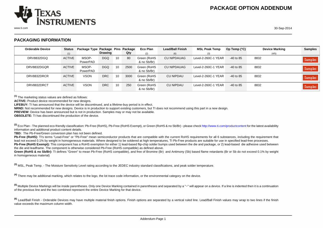
PACKAGING INFORMATION
Orderable Device Status(1)
Package Type PackageDrawing
Pins PackageQty
Eco Plan(2)
Lead/Ball Finish(6)
MSL Peak Temp(3)
Op Temp (°C) Device Marking(4/5)
Samples
DRV8832DGQ ACTIVE MSOP-PowerPAD
DGQ 10 80 Green (RoHS& no Sb/Br)
CU NIPDAUAG Level-2-260C-1 YEAR -40 to 85 8832
DRV8832DGQR ACTIVE MSOP-PowerPAD
DGQ 10 2500 Green (RoHS& no Sb/Br)
CU NIPDAUAG Level-2-260C-1 YEAR -40 to 85 8832
DRV8832DRCR ACTIVE VSON DRC 10 3000 Green (RoHS& no Sb/Br)
CU NIPDAU Level-2-260C-1 YEAR -40 to 85 8832
DRV8832DRCT ACTIVE VSON DRC 10 250 Green (RoHS& no Sb/Br)
CU NIPDAU Level-2-260C-1 YEAR -40 to 85 8832
(1) The marketing status values are defined as follows:ACTIVE: Product device recommended for new designs.LIFEBUY: TI has announced that the device will be discontinued, and a lifetime-buy period is in effect.NRND: Not recommended for new designs. Device is in production to support existing customers, but TI does not recommend using this part in a new design.PREVIEW: Device has been announced but is not in production. Samples may or may not be available.OBSOLETE: TI has discontinued the production of the device.
(2) Eco Plan - The planned eco-friendly classification: Pb-Free (RoHS), Pb-Free (RoHS Exempt), or Green (RoHS & no Sb/Br) - please check http://www.ti.com/productcontent for the latest availabilityinformation and additional product content details.TBD: The Pb-Free/Green conversion plan has not been defined.Pb-Free (RoHS): TI's terms "Lead-Free" or "Pb-Free" mean semiconductor products that are compatible with the current RoHS requirements for all 6 substances, including the requirement thatlead not exceed 0.1% by weight in homogeneous materials. Where designed to be soldered at high temperatures, TI Pb-Free products are suitable for use in specified lead-free processes.Pb-Free (RoHS Exempt): This component has a RoHS exemption for either 1) lead-based flip-chip solder bumps used between the die and package, or 2) lead-based die adhesive used betweenthe die and leadframe. The component is otherwise considered Pb-Free (RoHS compatible) as defined above.Green (RoHS & no Sb/Br): TI defines "Green" to mean Pb-Free (RoHS compatible), and free of Bromine (Br) and Antimony (Sb) based flame retardants (Br or Sb do not exceed 0.1% by weightin homogeneous material)
(3) MSL, Peak Temp. - The Moisture Sensitivity Level rating according to the JEDEC industry standard classifications, and peak solder temperature.
(4) There may be additional marking, which relates to the logo, the lot trace code information, or the environmental category on the device.
(5) Multiple Device Markings will be inside parentheses. Only one Device Marking contained in parentheses and separated by a "~" will appear on a device. If a line is indented then it is a continuationof the previous line and the two combined represent the entire Device Marking for that device.
(6) Lead/Ball Finish - Orderable Devices may have multiple material finish options. Finish options are separated by a vertical ruled line. Lead/Ball Finish values may wrap to two lines if the finishvalue exceeds the maximum column width.
PACKAGE OPTION ADDENDUM
www.ti.com 30-Sep-2014
Addendum-Page 2
Important Information and Disclaimer:The information provided on this page represents TI's knowledge and belief as of the date that it is provided. TI bases its knowledge and belief on informationprovided by third parties, and makes no representation or warranty as to the accuracy of such information. Efforts are underway to better integrate information from third parties. TI has taken andcontinues to take reasonable steps to provide representative and accurate information but may not have conducted destructive testing or chemical analysis on incoming materials and chemicals.TI and TI suppliers consider certain information to be proprietary, and thus CAS numbers and other limited information may not be available for release.
In no event shall TI's liability arising out of such information exceed the total purchase price of the TI part(s) at issue in this document sold by TI to Customer on an annual basis.
OTHER QUALIFIED VERSIONS OF DRV8832 :
• Automotive: DRV8832-Q1
NOTE: Qualified Version Definitions:
• Automotive - Q100 devices qualified for high-reliability automotive applications targeting zero defects
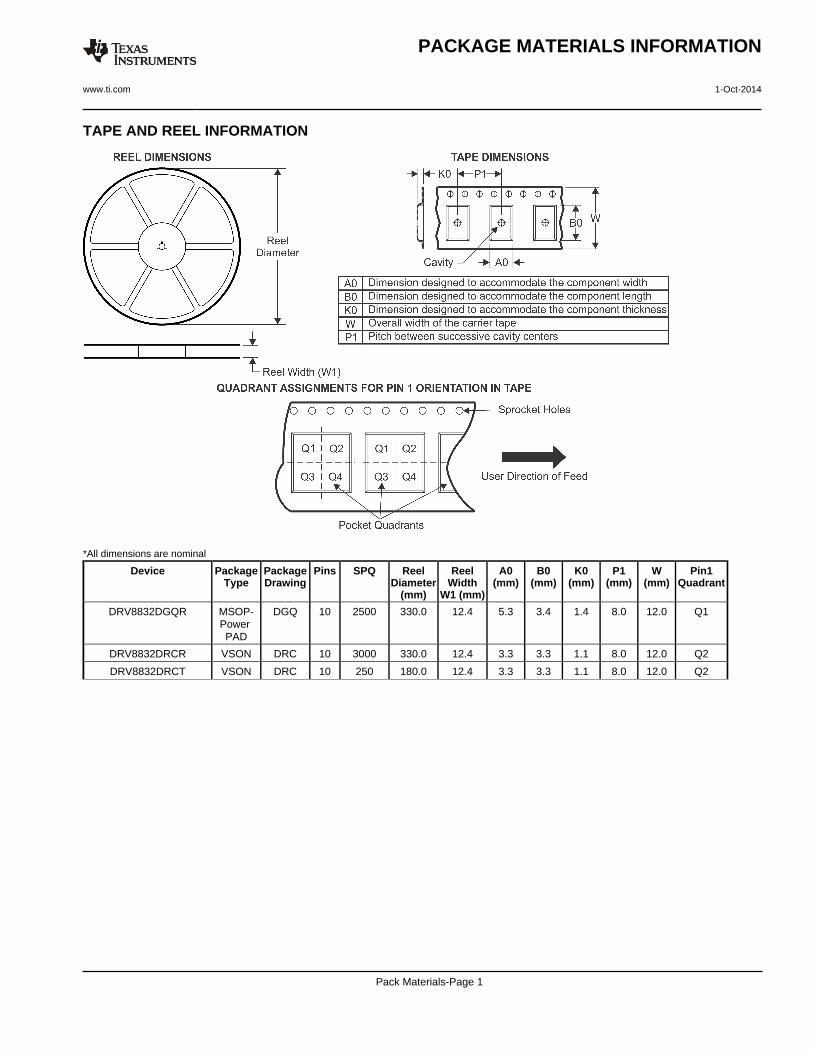
TAPE AND REEL INFORMATION
*All dimensions are nominal
Device PackageType
PackageDrawing
Pins SPQ ReelDiameter
(mm)
ReelWidth
W1 (mm)
A0(mm)
B0(mm)
K0(mm)
P1(mm)
W(mm)
Pin1Quadrant
DRV8832DGQR MSOP-Power PAD
DGQ 10 2500 330.0 12.4 5.3 3.4 1.4 8.0 12.0 Q1
DRV8832DRCR VSON DRC 10 3000 330.0 12.4 3.3 3.3 1.1 8.0 12.0 Q2
DRV8832DRCT VSON DRC 10 250 180.0 12.4 3.3 3.3 1.1 8.0 12.0 Q2
PACKAGE MATERIALS INFORMATION
www.ti.com 1-Oct-2014
Pack Materials-Page 1
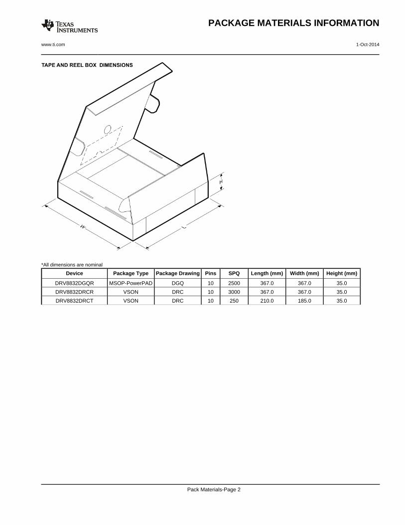
*All dimensions are nominal
Device Package Type Package Drawing Pins SPQ Length (mm) Width (mm) Height (mm)
DRV8832DGQR MSOP-PowerPAD DGQ 10 2500 367.0 367.0 35.0
DRV8832DRCR VSON DRC 10 3000 367.0 367.0 35.0
DRV8832DRCT VSON DRC 10 250 210.0 185.0 35.0
PACKAGE MATERIALS INFORMATION
www.ti.com 1-Oct-2014
Pack Materials-Page 2

IMPORTANT NOTICETexas Instruments Incorporated and its subsidiaries (TI) reserve the right to make corrections, enhancements, improvements and otherchanges to its semiconductor products and services per JESD46, latest issue, and to discontinue any product or service per JESD48, latestissue. Buyers should obtain the latest relevant information before placing orders and should verify that such information is current andcomplete. All semiconductor products (also referred to herein as “components”) are sold subject to TI’s terms and conditions of salesupplied at the time of order acknowledgment.TI warrants performance of its components to the specifications applicable at the time of sale, in accordance with the warranty in TI’s termsand conditions of sale of semiconductor products. Testing and other quality control techniques are used to the extent TI deems necessaryto support this warranty. Except where mandated by applicable law, testing of all parameters of each component is not necessarilyperformed.TI assumes no liability for applications assistance or the design of Buyers’ products. Buyers are responsible for their products andapplications using TI components. To minimize the risks associated with Buyers’ products and applications, Buyers should provideadequate design and operating safeguards.TI does not warrant or represent that any license, either express or implied, is granted under any patent right, copyright, mask work right, orother intellectual property right relating to any combination, machine, or process in which TI components or services are used. Informationpublished by TI regarding third-party products or services does not constitute a license to use such products or services or a warranty orendorsement thereof. Use of such information may require a license from a third party under the patents or other intellectual property of thethird party, or a license from TI under the patents or other intellectual property of TI.Reproduction of significant portions of TI information in TI data books or data sheets is permissible only if reproduction is without alterationand is accompanied by all associated warranties, conditions, limitations, and notices. TI is not responsible or liable for such altereddocumentation. Information of third parties may be subject to additional restrictions.Resale of TI components or services with statements different from or beyond the parameters stated by TI for that component or servicevoids all express and any implied warranties for the associated TI component or service and is an unfair and deceptive business practice.TI is not responsible or liable for any such statements.Buyer acknowledges and agrees that it is solely responsible for compliance with all legal, regulatory and safety-related requirementsconcerning its products, and any use of TI components in its applications, notwithstanding any applications-related information or supportthat may be provided by TI. Buyer represents and agrees that it has all the necessary expertise to create and implement safeguards whichanticipate dangerous consequences of failures, monitor failures and their consequences, lessen the likelihood of failures that might causeharm and take appropriate remedial actions. Buyer will fully indemnify TI and its representatives against any damages arising out of the useof any TI components in safety-critical applications.In some cases, TI components may be promoted specifically to facilitate safety-related applications. With such components, TI’s goal is tohelp enable customers to design and create their own end-product solutions that meet applicable functional safety standards andrequirements. Nonetheless, such components are subject to these terms.No TI components are authorized for use in FDA Class III (or similar life-critical medical equipment) unless authorized officers of the partieshave executed a special agreement specifically governing such use.Only those TI components which TI has specifically designated as military grade or “enhanced plastic” are designed and intended for use inmilitary/aerospace applications or environments. Buyer acknowledges and agrees that any military or aerospace use of TI componentswhich have not been so designated is solely at the Buyer's risk, and that Buyer is solely responsible for compliance with all legal andregulatory requirements in connection with such use.TI has specifically designated certain components as meeting ISO/TS16949 requirements, mainly for automotive use. In any case of use ofnon-designated products, TI will not be responsible for any failure to meet ISO/TS16949.Products ApplicationsAudio www.ti.com/audio Automotive and Transportation www.ti.com/automotiveAmplifiers amplifier.ti.com Communications and Telecom www.ti.com/communicationsData Converters dataconverter.ti.com Computers and Peripherals www.ti.com/computersDLP® Products www.dlp.com Consumer Electronics www.ti.com/consumer-appsDSP dsp.ti.com Energy and Lighting www.ti.com/energyClocks and Timers www.ti.com/clocks Industrial www.ti.com/industrialInterface interface.ti.com Medical www.ti.com/medicalLogic logic.ti.com Security www.ti.com/securityPower Mgmt power.ti.com Space, Avionics and Defense www.ti.com/space-avionics-defenseMicrocontrollers microcontroller.ti.com Video and Imaging www.ti.com/videoRFID www.ti-rfid.comOMAP Applications Processors www.ti.com/omap TI E2E Community e2e.ti.comWireless Connectivity www.ti.com/wirelessconnectivity
Mailing Address: Texas Instruments, Post Office Box 655303, Dallas, Texas 75265Copyright © 2014, Texas Instruments Incorporated