low-power digital cmos design: a survey · low-power digital cmos design: a survey krister...
TRANSCRIPT
Low-Power Digital CMOS Design: A Survey
Krister Landernas ∗
June 14, 2005
∗Department of Computer Science and Electronics, Malardalen University

Abstract
The aim of this document is to provide the reader with an overview oflow-power digital design trends. Several research publications and bookshave been studied by the author and the knowledge gained has been com-piled into this report. Low-power techniques adopted at different levels ofthe design process are presented and industrial application examples aregiven.
Contents
1 Motivation 1
2 Introduction 1
3 Technology Optimization 3
4 Logic Optimization 4
5 Architecture Optimization 5
6 System Optimization 6
7 Conclusions 9
1 Motivation
In the last decade, low-power has become an important goal when designing dig-ital systems. There are several reasons for this. The main motivation is perhapsthe increasing market for portable electronic devices. Lap-top computers, cellu-lar phones and MP3 players are today common consumer products. Maintainingreasonable battery life-time with an increasing number of functions integratedin these products requires a low-power design approach. The fact that batterylife-times are only predicted to increase with 30-40% over the next years onlyfurther emphasises the need for low-power designs [1].
Decreasing the power consumption is also important in applications whichare not battery-powered, e.g. stationary computers. Today, the power con-sumption for high-performance microprocessors can exceed 100 Watt. Withoutcooling the circuit would literally start to burn. Much time and effort is spenton packaging and cooling in order to remove superfluous heat. This increasesdeveloping time and the total manufacturing cost for the application.
2 Introduction
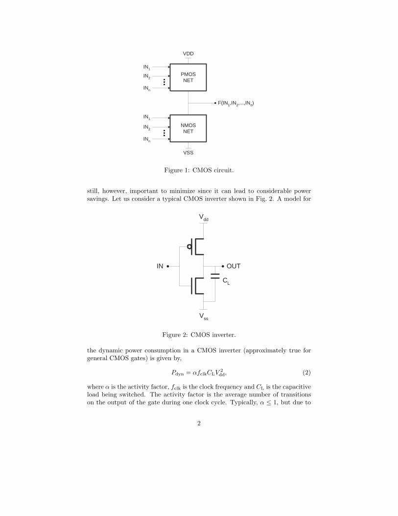
In this report, we study the power consumption of digital CMOS (complemen-tary metal oxide semiconductor) circuits. Today, the majority of digital ICsare manufactured using CMOS, although there are exceptions (e.g. BiCMOS).This was not the case in the 70’s, when most digital circuits were realized us-ing only NMOS technology. The change into using complementary logic (bothPMOS and NMOS) was caused by the fact that the static power consumptionfor NMOS circuits became too high. The solution was to use CMOS circuitswhich have (ideally) no direct path between power supply and ground in steadystate and, hence, no static power consumption. This is illustrated in Fig. 1,where a typical CMOS circuit is shown. Note that the PMOS and NMOS netcannot conduct simultaneously.
The power consumption for a CMOS circuit can be expressed as,
P = Pdyn + Pstat + Pshort + Pleak, (1)
where Pdyn is the dynamic power consumption caused by charging and discharg-ing capacitors driven by the circuit. Ideally the PMOS and NMOS net (see Fig.1) cannot conduct at the same time. Unfortunately, a transistor is not an idealswitch and as a result a current will flow between the rails in steady state. Thiscurrent causes a static power consumption Pstat. During input transitions thePMOS and NMOS net can, for a short time period, conduct simultaneouslyresulting in a short-circuit dissipation Pshort. Pleak is caused by substrate andsub-threshold currents. Note, some publications does not distinguish betweenPstat and Pleak.
Historically, for technologies above 0.8µm, Pdyn dominated the total powerconsumption (over 90%). This is no longer the case as Pleak becomes moresignificant in deep-submicron technologies. The dynamic power consumption is
1
PMOSNET
IN1
IN2
INn
NMOSNET
IN1
IN2
INn
VDD
VSS
F(IN1,IN2,...,INn)
Figure 1: CMOS circuit.
still, however, important to minimize since it can lead to considerable powersavings. Let us consider a typical CMOS inverter shown in Fig. 2. A model for
CL
Vdd
Vss
IN OUT
Figure 2: CMOS inverter.
the dynamic power consumption in a CMOS inverter (approximately true forgeneral CMOS gates) is given by,
Pdyn = αfclkCLV 2dd, (2)
where α is the activity factor, fclk is the clock frequency and CL is the capacitiveload being switched. The activity factor is the average number of transitionson the output of the gate during one clock cycle. Typically, α ≤ 1, but due to
2
glitches some systems may experience an activity factor larger than one. From(2), we have three parameters that we can target when trying to minimize thedynamic power consumption. The switching activity, i.e. αfclk, the capacitiveload and the voltage supply level. Their influence on the total power consump-tion and how we can affect these parameters will become clear in the followingsections.
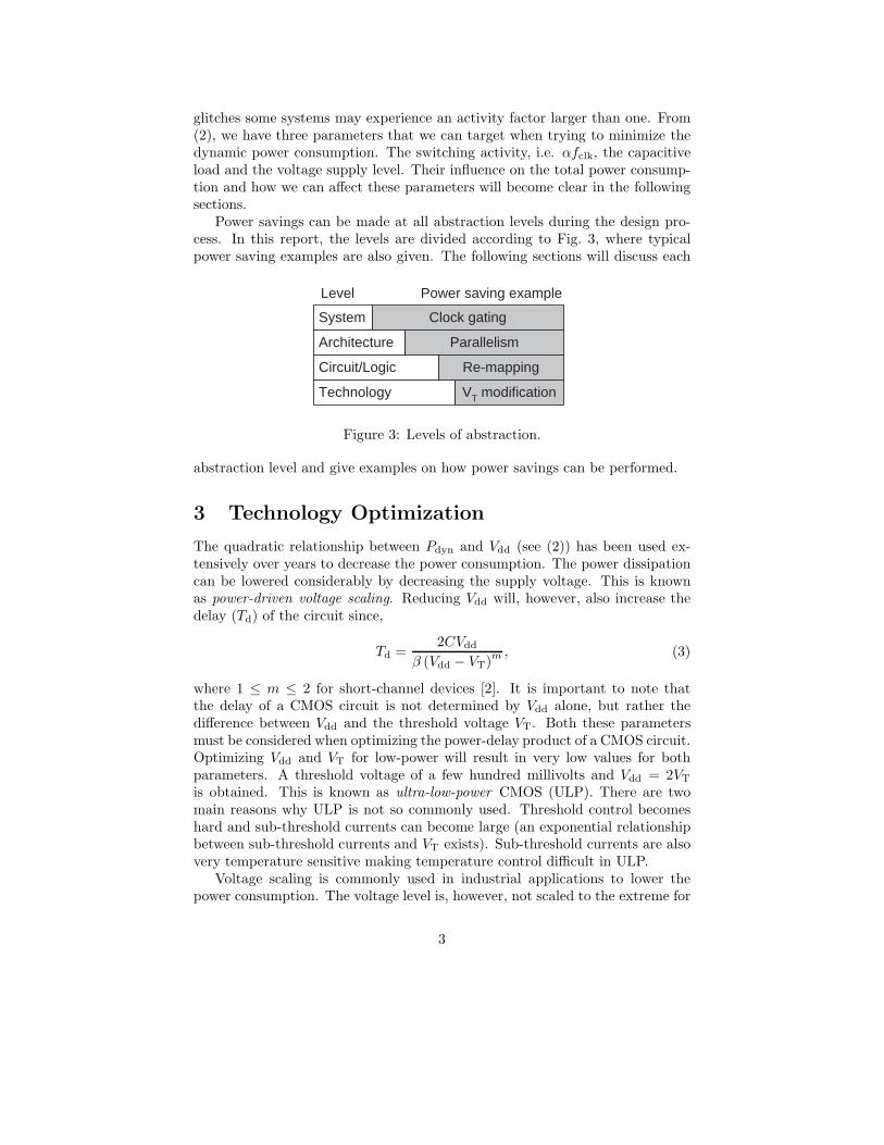
Power savings can be made at all abstraction levels during the design pro-cess. In this report, the levels are divided according to Fig. 3, where typicalpower saving examples are also given. The following sections will discuss each
System
Architecture
Circuit/Logic
Technology VT modification
Re-mapping
Parallelism
Clock gating
Level Power saving example
Figure 3: Levels of abstraction.
abstraction level and give examples on how power savings can be performed.
3 Technology Optimization
The quadratic relationship between Pdyn and Vdd (see (2)) has been used ex-tensively over years to decrease the power consumption. The power dissipationcan be lowered considerably by decreasing the supply voltage. This is knownas power-driven voltage scaling. Reducing Vdd will, however, also increase thedelay (Td) of the circuit since,
Td =2CVdd
β (Vdd − VT)m , (3)
where 1 ≤ m ≤ 2 for short-channel devices [2]. It is important to note thatthe delay of a CMOS circuit is not determined by Vdd alone, but rather thedifference between Vdd and the threshold voltage VT. Both these parametersmust be considered when optimizing the power-delay product of a CMOS circuit.Optimizing Vdd and VT for low-power will result in very low values for bothparameters. A threshold voltage of a few hundred millivolts and Vdd = 2VT
is obtained. This is known as ultra-low-power CMOS (ULP). There are twomain reasons why ULP is not so commonly used. Threshold control becomeshard and sub-threshold currents can become large (an exponential relationshipbetween sub-threshold currents and VT exists). Sub-threshold currents are alsovery temperature sensitive making temperature control difficult in ULP.
Voltage scaling is commonly used in industrial applications to lower thepower consumption. The voltage level is, however, not scaled to the extreme for
3
reasons stated above. In Example 1 an application where voltage scaling wasused is shown.
Example 1:The StrongARM processor was designed in a three-metal layer 0.35µm pro-cess. It was later developed for low-power, where the voltage supply wasscaled from 3.45 V to 1.5 V with VT = 0.35V . A power reduction of 5.3times was obtained [3].
In high-performance systems, the power consumption generated by leakagecurrents is becoming an increasing problem. Fast transistors with low thresh-old voltages generate high static currents. One solution to the problem is touse a dual threshold logic. High-performance parts of a system can then beimplemented using low-threshold devices while subsystems that are not timingcritical can use a higher threshold level. A more dynamic solution is to increasethe threshold level when the system, or parts of it, is in standby. Changing thethreshold level is commonly realized by applying substrate biasing, see Example2.
Example 2:The MPEG4 Video Codec prototype adopted the variable threshold voltagescheme to reduce power dissipation. Substrate biasing is exploited to dy-namically adjust the threshold. VT is set to 0.2 V in active mode and 0.55V in standby mode [3].
4 Logic Optimization
A number of logic optimization techniques for low-power have been developedover the years. These methods usually target either the switching activity or thecapacitance of the logic. Today, due to design complexity, most logic optimiza-tion is done by synthesis tools. Fortunately many of the low-power methodsdiscussed in this section can be performed by the tools.
Traditional cell libraries were developed for high-speed. This implies largetransistors with high power consumption. Libraries with low-power capabilitiesare, however, becoming more common. Usually a low-power model of each cellis included in the library. This cell is optimized with smaller transistor sizes andshorter interconnect. In a synchronous design the number of flip-flops is usuallylarge. It is therefore important that the library contains registers optimizedfor low-power. Naturally, the synthesis tool must include power optimizationroutines in order to take advantage of a low-power library.
The synthesis tool will try to minimize power consumption after all timingrequirements are met. This is done by replacing cells in the netlist to decreasethe power consumption. Any replacement that lead to better power character-istics without violating timing will be accepted. This procedure is known asre-mapping. Re-mapping may cause a cell to be resized or a group of cells to be
4
replaced with a more complex cell. This is an intricate optimization probleminvolving both switching power as well as internal power on a number of cellsat the same time.
In addition to re-mapping, pin swapping is also used to minimize powerdissipation. Pin swapping changes the input order to connect signals with highactivity to low-capacitance inputs. Both re-mapping and pin swapping are timeconsuming operations which are applied to local parts of a netlist. As a resultthe power savings are quite small with 10-20% savings usually obtained.
5 Architecture Optimization
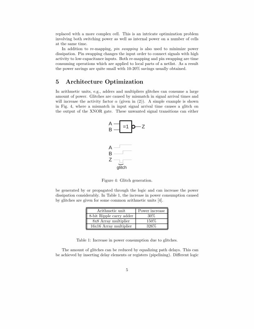
In arithmetic units, e.g., adders and multipliers glitches can consume a largeamount of power. Glitches are caused by mismatch in signal arrival times andwill increase the activity factor α (given in (2)). A simple example is shownin Fig. 4, where a mismatch in input signal arrival time causes a glitch onthe output of the XNOR gate. These unwanted signal transitions can either
=1AB
Z
ABZ
{
glitch
Figure 4: Glitch generation.
be generated by or propagated through the logic and can increase the powerdissipation considerably. In Table 1, the increase in power consumption causedby glitches are given for some common arithmetic units [4].
Arithmetic unit Power increase8-bit Ripple carry adder 30%
8x8 Array multiplier 150%16x16 Array multiplier 326%
Table 1: Increase in power consumption due to glitches.
The amount of glitches can be reduced by equalizing path delays. This canbe achieved by inserting delay elements or registers (pipelining). Different logic
5
units can be more or less prone to generate glitches. A Wallace-tree multiplierhas more balanced paths than an Array multiplier and will, therefore, experi-ence fewer glitches (see Example 3).
Example 3:The MAC unit in the StrongARM processor is based on a Wallace-treemultiplier and a Carry-look-ahead adder. Power savings of 23% were madecompared to using an Array multiplier [3].
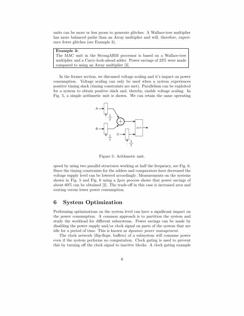
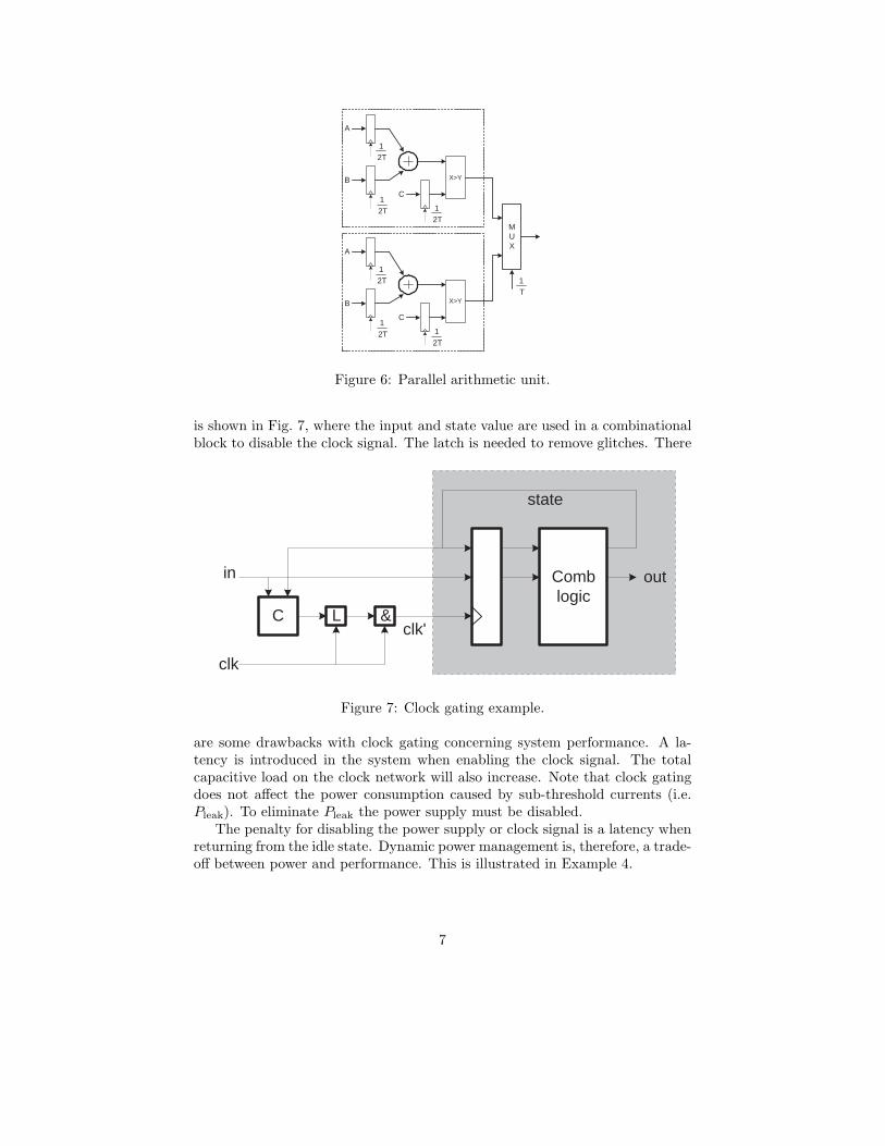
In the former section, we discussed voltage scaling and it’s impact on powerconsumption. Voltage scaling can only be used when a system experiencespositive timing slack (timing constraints are met). Parallelism can be exploitedfor a system to obtain positive slack and, thereby, enable voltage scaling. InFig. 5, a simple arithmetic unit is shown. We can retain the same operating
1T
A
1T
B
1T
C
X>Y
Figure 5: Arithmetic unit.
speed by using two parallel structures working at half the frequency, see Fig. 6.Since the timing constraints for the adders and comparators have decreased thevoltage supply level can be lowered accordingly. Measurements on the systemsshown in Fig. 5 and Fig. 6 using a 2µm process shows that power savings ofabout 60% can be obtained [2]. The trade-off in this case is increased area androuting versus lower power consumption.
6 System Optimization
Performing optimizations on the system level can have a significant impact onthe power consumption. A common approach is to partition the system andstudy the workload for different subsystems. Power savings can be made bydisabling the power supply and/or clock signal on parts of the system that areidle for a period of time. This is known as dynamic power management.
The clock network (flip-flops, buffers) of a subsystem will consume powereven if the system performs no computation. Clock gating is used to preventthis by turning off the clock signal to inactive blocks. A clock gating example
6
12T
A
B
C
X>Y
MUX
12T 1
2T
12T
A
B
C
X>Y
12T 1
2T
1T
Figure 6: Parallel arithmetic unit.
is shown in Fig. 7, where the input and state value are used in a combinationalblock to disable the clock signal. The latch is needed to remove glitches. There
Comblogic
clk
Lclk'
outin
&C
state
Figure 7: Clock gating example.
are some drawbacks with clock gating concerning system performance. A la-tency is introduced in the system when enabling the clock signal. The totalcapacitive load on the clock network will also increase. Note that clock gatingdoes not affect the power consumption caused by sub-threshold currents (i.e.Pleak). To eliminate Pleak the power supply must be disabled.
The penalty for disabling the power supply or clock signal is a latency whenreturning from the idle state. Dynamic power management is, therefore, a trade-off between power and performance. This is illustrated in Example 4.
7
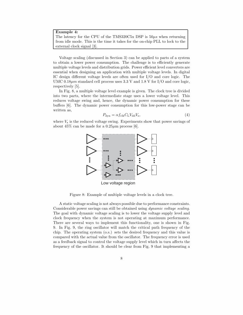
Example 4:The latency for the CPU of the TMS320C5x DSP is 50µs when returningfrom idle mode. This is the time it takes for the on-chip PLL to lock to theexternal clock signal [3].
Voltage scaling (discussed in Section 3) can be applied to parts of a systemto obtain a lower power consumption. The challenge is to efficiently generatemultiple voltage levels and distribution grids. Power efficient level converters areessential when designing an application with multiple voltage levels. In digitalIC design different voltage levels are often used for I/O and core logic. TheUMC 0.18µm standard cell process uses 3.3 V and 1.8 V for I/O and core logic,respectively [5].
In Fig. 8, a multiple voltage level example is given. The clock tree is dividedinto two parts, where the intermediate stage uses a lower voltage level. Thisreduces voltage swing and, hence, the dynamic power consumption for thesebuffers [6]. The dynamic power consumption for this low-power stage can bewritten as,
Pdyn = αfclkCLVddVs, (4)
where Vs is the reduced voltage swing. Experiments show that power savings ofabout 45% can be made for a 0.25µm process [6].
Low voltage region
Figure 8: Example of multiple voltage levels in a clock tree.
A static voltage scaling is not always possible due to performance constraints.Considerable power savings can still be obtained using dynamic voltage scaling.The goal with dynamic voltage scaling is to lower the voltage supply level andclock frequency when the system is not operating at maximum performance.There are several ways to implement this functionality, one is shown in Fig.9. In Fig. 9, the ring oscillator will match the critical path frequency of thechip. The operating system (o.s.) sets the desired frequency and this value iscompared with the actual value from the oscillator. The frequency error is usedas a feedback signal to control the voltage supply level which in turn affects thefrequency of the oscillator. It should be clear from Fig. 9 that implementing a
8
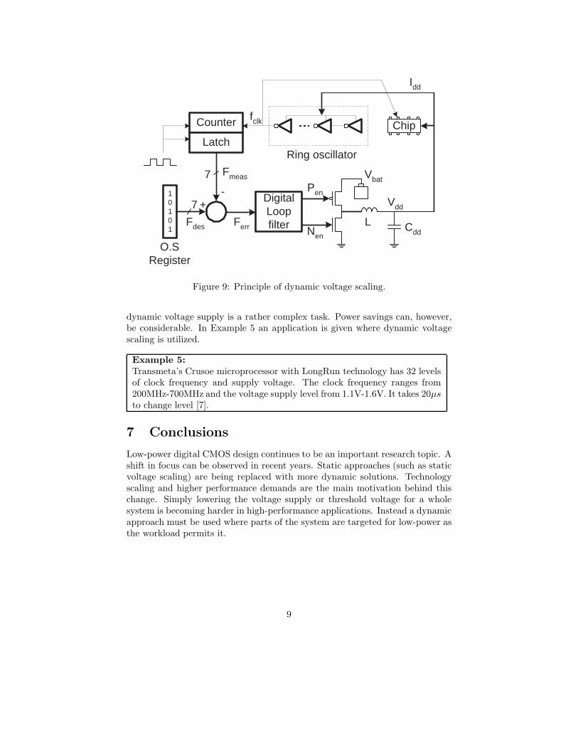
Ring oscillator
fclkCounter
Latch
10101
O.SRegister
7
7
Fdes
Fmeas
+- Digital
LoopfilterFerr
Pen
Nen
Chip
Idd
L Cdd
Vdd
Vbat
Figure 9: Principle of dynamic voltage scaling.
dynamic voltage supply is a rather complex task. Power savings can, however,be considerable. In Example 5 an application is given where dynamic voltagescaling is utilized.
Example 5:Transmeta’s Crusoe microprocessor with LongRun technology has 32 levelsof clock frequency and supply voltage. The clock frequency ranges from200MHz-700MHz and the voltage supply level from 1.1V-1.6V. It takes 20µsto change level [7].
7 Conclusions
Low-power digital CMOS design continues to be an important research topic. Ashift in focus can be observed in recent years. Static approaches (such as staticvoltage scaling) are being replaced with more dynamic solutions. Technologyscaling and higher performance demands are the main motivation behind thischange. Simply lowering the voltage supply or threshold voltage for a wholesystem is becoming harder in high-performance applications. Instead a dynamicapproach must be used where parts of the system are targeted for low-power asthe workload permits it.
9
References
[1] J. M. Rabaey, A. Chandrakasan and B. Nikolic, Digital Integrated Circuits,Prentice Hall, 2003.
[2] A. Chandrakasan and R. W. Brodersen, “Minimizing power consumptionon digital CMOS circuits,” IEEE Proceedings, Vol-83, Issue. 4, pp. 498–523,April 1995.
[3] L. Benini, G. De Micheli and E. Macii, “Designing low-power circuits: prac-tical recipes,” IEEE Circuits and Systems Magazine, Vol-1, Issue. 1, pp.6–25, 2001.
[4] H. Veendrick, Deep-Submicron CMOS IC’s, Kluwer, 2000.
[5] High Performance 0.18µ Standard cell library data book, Rev.2.1, VirtualSilicon Technology, Inc., Sunnyvale, CA, January 2001.
[6] J. Pangjun and S. S. Sapatnekar, “Low-power clock distribution using mul-tiple voltages and reduced swings,” IEEE Trans. on Very Large Scale In-tegration (VLSI) Systems, Vol-10, No. 3, pp. 309–318, June 2002.
[7] Crusoe Processor model TM5700/TM5900 databook, Rev.1.0, TransmetaCorporation, 2004.
10