logicore™ ethernet 1000base-x pcs/pma or … · ethernet 1000base-x pcs/pma or sgmii v7.0 13...
TRANSCRIPT
R
LogiCORE™ Ethernet 1000BASE-X PCS/PMA or SGMII v7.0
Getting Started GuideUG145 January 18, 2006

www.xilinx.com Ethernet 1000BASE-X PCS/PMA or SGMII v7.0UG145 January 18, 2006
Xilinx is disclosing this Document and Intellectual Property (hereinafter “the Design”) to you for use in the development of designs to operate on, or interface with Xilinx FPGAs. Except as stated herein, none of the Design may be copied, reproduced, distributed, republished, downloaded, displayed, posted, or transmitted in any form or by any means including, but not limited to, electronic, mechanical, photocopying, recording, or otherwise, without the prior written consent of Xilinx. Any unauthorized use of the Design may violate copyright laws, trademark laws, the laws of privacy and publicity, and communications regulations and statutes.
Xilinx does not assume any liability arising out of the application or use of the Design; nor does Xilinx convey any license under its patents, copyrights, or any rights of others. You are responsible for obtaining any rights you may require for your use or implementation of the Design. Xilinx reserves the right to make changes, at any time, to the Design as deemed desirable in the sole discretion of Xilinx. Xilinx assumes no obligation to correct any errors contained herein or to advise you of any correction if such be made. Xilinx will not assume any liability for the accuracy or correctness of any engineering or technical support or assistance provided to you in connection with the Design.
THE DESIGN IS PROVIDED “AS IS" WITH ALL FAULTS, AND THE ENTIRE RISK AS TO ITS FUNCTION AND IMPLEMENTATION IS WITH YOU. YOU ACKNOWLEDGE AND AGREE THAT YOU HAVE NOT RELIED ON ANY ORAL OR WRITTEN INFORMATION OR ADVICE, WHETHER GIVEN BY XILINX, OR ITS AGENTS OR EMPLOYEES. XILINX MAKES NO OTHER WARRANTIES, WHETHER EXPRESS, IMPLIED, OR STATUTORY, REGARDING THE DESIGN, INCLUDING ANY WARRANTIES OF MERCHANTABILITY, FITNESS FOR A PARTICULAR PURPOSE, TITLE, AND NONINFRINGEMENT OF THIRD-PARTY RIGHTS.
IN NO EVENT WILL XILINX BE LIABLE FOR ANY CONSEQUENTIAL, INDIRECT, EXEMPLARY, SPECIAL, OR INCIDENTAL DAMAGES, INCLUDING ANY LOST DATA AND LOST PROFITS, ARISING FROM OR RELATING TO YOUR USE OF THE DESIGN, EVEN IF YOU HAVE BEEN ADVISED OF THE POSSIBILITY OF SUCH DAMAGES. THE TOTAL CUMULATIVE LIABILITY OF XILINX IN CONNECTION WITH YOUR USE OF THE DESIGN, WHETHER IN CONTRACT OR TORT OR OTHERWISE, WILL IN NO EVENT EXCEED THE AMOUNT OF FEES PAID BY YOU TO XILINX HEREUNDER FOR USE OF THE DESIGN. YOU ACKNOWLEDGE THAT THE FEES, IF ANY, REFLECT THE ALLOCATION OF RISK SET FORTH IN THIS AGREEMENT AND THAT XILINX WOULD NOT MAKE AVAILABLE THE DESIGN TO YOU WITHOUT THESE LIMITATIONS OF LIABILITY.
The Design is not designed or intended for use in the development of on-line control equipment in hazardous environments requiring fail-safe controls, such as in the operation of nuclear facilities, aircraft navigation or communications systems, air traffic control, life support, or weapons systems (“High-Risk Applications”). Xilinx specifically disclaims any express or implied warranties of fitness for such High-Risk Applications. You represent that use of the Design in such High-Risk Applications is fully at your risk.
© 2006 Xilinx, Inc. All rights reserved. XILINX, the Xilinx logo, and other designated brands included herein are trademarks of Xilinx, Inc. All other trademarks are the property of their respective owners.
R
Ethernet 1000BASE-X PCS/PMA or SGMII v7.0 www.xilinx.comUG145 January 18, 2006
Ethernet 1000BASE-X PCS/PMA or SGMII v7.0 Getting Started GuideUG145 January 18, 2006
The following table shows the revision history for this document.
Date Version Revision
09/30/04 1.0 Initial Xilinx release.
04/28/05 2.0 Updated to version 6.0 of the core, and Xilinx Tools v7.1i SP2.
01/18/06 3.0 Updated to version 7.0 of the core, and Xilinx Tools v8.1i, updated Licensing chapter.

www.xilinx.com Ethernet 1000BASE-X PCS/PMA or SGMII v7.0UG145 January 18, 2006
Ethernet 1000BASE-X PCS/PMA or SGMII v7.0 www.xilinx.com 5UG145 January 18, 2006
Schedule of Figures . . . . . . . . . . . . . . . . . . . . . . . . . . . . . . . . . . . . . . . . . . . . . . . . . . . . . . . . . . 7
Preface: About This GuideGuide Contents . . . . . . . . . . . . . . . . . . . . . . . . . . . . . . . . . . . . . . . . . . . . . . . . . . . . . . . . . . . . . . 9Additional Resources . . . . . . . . . . . . . . . . . . . . . . . . . . . . . . . . . . . . . . . . . . . . . . . . . . . . . . . . 9Conventions . . . . . . . . . . . . . . . . . . . . . . . . . . . . . . . . . . . . . . . . . . . . . . . . . . . . . . . . . . . . . . . . 10
Typographical . . . . . . . . . . . . . . . . . . . . . . . . . . . . . . . . . . . . . . . . . . . . . . . . . . . . . . . . . . . . 10Online Document . . . . . . . . . . . . . . . . . . . . . . . . . . . . . . . . . . . . . . . . . . . . . . . . . . . . . . . . . 11
Chapter 1: IntroductionAbout the Core . . . . . . . . . . . . . . . . . . . . . . . . . . . . . . . . . . . . . . . . . . . . . . . . . . . . . . . . . . . . . . 13Recommended Design Experience . . . . . . . . . . . . . . . . . . . . . . . . . . . . . . . . . . . . . . . . . . . 13Additional Core Resources . . . . . . . . . . . . . . . . . . . . . . . . . . . . . . . . . . . . . . . . . . . . . . . . . . 13Technical Support. . . . . . . . . . . . . . . . . . . . . . . . . . . . . . . . . . . . . . . . . . . . . . . . . . . . . . . . . . . 14Feedback. . . . . . . . . . . . . . . . . . . . . . . . . . . . . . . . . . . . . . . . . . . . . . . . . . . . . . . . . . . . . . . . . . . . 14
Ethernet 1000BASE-X PCS/PMA or SGMII Core . . . . . . . . . . . . . . . . . . . . . . . . . . . . . . 14Document . . . . . . . . . . . . . . . . . . . . . . . . . . . . . . . . . . . . . . . . . . . . . . . . . . . . . . . . . . . . . . . 14
Chapter 2: Installing and Licensing the CoreSystem Requirements . . . . . . . . . . . . . . . . . . . . . . . . . . . . . . . . . . . . . . . . . . . . . . . . . . . . . . . 15Before You Begin . . . . . . . . . . . . . . . . . . . . . . . . . . . . . . . . . . . . . . . . . . . . . . . . . . . . . . . . . . . 15Installing the Core . . . . . . . . . . . . . . . . . . . . . . . . . . . . . . . . . . . . . . . . . . . . . . . . . . . . . . . . . . 15
CORE Generator IP Updates Installer . . . . . . . . . . . . . . . . . . . . . . . . . . . . . . . . . . . . . . . 16Manual Installation . . . . . . . . . . . . . . . . . . . . . . . . . . . . . . . . . . . . . . . . . . . . . . . . . . . . . . . 16
Verifying the Installation . . . . . . . . . . . . . . . . . . . . . . . . . . . . . . . . . . . . . . . . . . . . . . . . . . . 17License Options . . . . . . . . . . . . . . . . . . . . . . . . . . . . . . . . . . . . . . . . . . . . . . . . . . . . . . . . . . . . . 17
Simulation Only . . . . . . . . . . . . . . . . . . . . . . . . . . . . . . . . . . . . . . . . . . . . . . . . . . . . . . . . . . 18Full . . . . . . . . . . . . . . . . . . . . . . . . . . . . . . . . . . . . . . . . . . . . . . . . . . . . . . . . . . . . . . . . . . . . . 18
Obtaining Your License . . . . . . . . . . . . . . . . . . . . . . . . . . . . . . . . . . . . . . . . . . . . . . . . . . . . . 18Installing the License File . . . . . . . . . . . . . . . . . . . . . . . . . . . . . . . . . . . . . . . . . . . . . . . . . . . 18
Chapter 3: Quick Start Example DesignOverview . . . . . . . . . . . . . . . . . . . . . . . . . . . . . . . . . . . . . . . . . . . . . . . . . . . . . . . . . . . . . . . . . . . 19Generating the Core . . . . . . . . . . . . . . . . . . . . . . . . . . . . . . . . . . . . . . . . . . . . . . . . . . . . . . . . . 20Implementing the Example Design . . . . . . . . . . . . . . . . . . . . . . . . . . . . . . . . . . . . . . . . . . 21Simulating the Example Design . . . . . . . . . . . . . . . . . . . . . . . . . . . . . . . . . . . . . . . . . . . . . 21
Setting up for Simulation . . . . . . . . . . . . . . . . . . . . . . . . . . . . . . . . . . . . . . . . . . . . . . . . . . 21Functional Simulation . . . . . . . . . . . . . . . . . . . . . . . . . . . . . . . . . . . . . . . . . . . . . . . . . . . . . 21Timing Simulation . . . . . . . . . . . . . . . . . . . . . . . . . . . . . . . . . . . . . . . . . . . . . . . . . . . . . . . . 22
What’s Next? . . . . . . . . . . . . . . . . . . . . . . . . . . . . . . . . . . . . . . . . . . . . . . . . . . . . . . . . . . . . . . . . 22
Table of Contents
6 www.xilinx.com Ethernet 1000BASE-X PCS/PMA or SGMII v7.0UG145 January 18, 2006
R
Chapter 4: Detailed Example DesignDirectory Structure and File Descriptions . . . . . . . . . . . . . . . . . . . . . . . . . . . . . . . . . . . . 23
VHDL Design Entry . . . . . . . . . . . . . . . . . . . . . . . . . . . . . . . . . . . . . . . . . . . . . . . . . . . . . . 23Verilog Design Entry . . . . . . . . . . . . . . . . . . . . . . . . . . . . . . . . . . . . . . . . . . . . . . . . . . . . . . 27
Implementation Scripts . . . . . . . . . . . . . . . . . . . . . . . . . . . . . . . . . . . . . . . . . . . . . . . . . . . . . 30Simulation Scripts . . . . . . . . . . . . . . . . . . . . . . . . . . . . . . . . . . . . . . . . . . . . . . . . . . . . . . . . . . 30
Functional simulation . . . . . . . . . . . . . . . . . . . . . . . . . . . . . . . . . . . . . . . . . . . . . . . . . . . . . 30Timing simulation . . . . . . . . . . . . . . . . . . . . . . . . . . . . . . . . . . . . . . . . . . . . . . . . . . . . . . . . 31
Core Example Design Using RocketIO. . . . . . . . . . . . . . . . . . . . . . . . . . . . . . . . . . . . . . . 32Top-Level HDL. . . . . . . . . . . . . . . . . . . . . . . . . . . . . . . . . . . . . . . . . . . . . . . . . . . . . . . . . . . 32Transceiver . . . . . . . . . . . . . . . . . . . . . . . . . . . . . . . . . . . . . . . . . . . . . . . . . . . . . . . . . . . . . . 33Transmitter Elastic Buffer . . . . . . . . . . . . . . . . . . . . . . . . . . . . . . . . . . . . . . . . . . . . . . . . . . 33
Demonstration Test Bench . . . . . . . . . . . . . . . . . . . . . . . . . . . . . . . . . . . . . . . . . . . . . . . . . . 34Customizing the Test Bench . . . . . . . . . . . . . . . . . . . . . . . . . . . . . . . . . . . . . . . . . . . . . . . . 35
Core Example Design with Ten-Bit Interface. . . . . . . . . . . . . . . . . . . . . . . . . . . . . . . . . 36Example Design Top-Level HDL. . . . . . . . . . . . . . . . . . . . . . . . . . . . . . . . . . . . . . . . . . . . 36Transmitter Elastic Buffer . . . . . . . . . . . . . . . . . . . . . . . . . . . . . . . . . . . . . . . . . . . . . . . . . . 37Demonstration Test Bench . . . . . . . . . . . . . . . . . . . . . . . . . . . . . . . . . . . . . . . . . . . . . . . . . 38Customizing the Test Bench . . . . . . . . . . . . . . . . . . . . . . . . . . . . . . . . . . . . . . . . . . . . . . . . 39
SGMII Example Design / Dynamic Switching Example Design . . . . . . . . . . . . . . 40Example Design Top-Level HDL. . . . . . . . . . . . . . . . . . . . . . . . . . . . . . . . . . . . . . . . . . . . 40Transceiver . . . . . . . . . . . . . . . . . . . . . . . . . . . . . . . . . . . . . . . . . . . . . . . . . . . . . . . . . . . . . . 41SGMII Adaptation Module . . . . . . . . . . . . . . . . . . . . . . . . . . . . . . . . . . . . . . . . . . . . . . . . . 41Clock Generation . . . . . . . . . . . . . . . . . . . . . . . . . . . . . . . . . . . . . . . . . . . . . . . . . . . . . . . . . 43Johnson Counter . . . . . . . . . . . . . . . . . . . . . . . . . . . . . . . . . . . . . . . . . . . . . . . . . . . . . . . . . . 44Transmitter Rate Adaptation Module . . . . . . . . . . . . . . . . . . . . . . . . . . . . . . . . . . . . . . . . 45Receiver Rate Adaptation Module . . . . . . . . . . . . . . . . . . . . . . . . . . . . . . . . . . . . . . . . . . 46Demonstration Test Bench . . . . . . . . . . . . . . . . . . . . . . . . . . . . . . . . . . . . . . . . . . . . . . . . . 48Customizing the Test Bench . . . . . . . . . . . . . . . . . . . . . . . . . . . . . . . . . . . . . . . . . . . . . . . . 49
Ethernet 1000BASE-X PCS/PMA or SGMII v7.0 www.xilinx.com 7UG145 January 18, 2006
Chapter 1: Introduction
Chapter 2: Installing and Licensing the CoreFigure 2-1: CORE Generator Window . . . . . . . . . . . . . . . . . . . . . . . . . . . . . . . . . . . . . . . . . . . 17
Chapter 3: Quick Start Example DesignFigure 3-1: Ethernet 1000BASE-X PCS/PMA Example Design and Test Bench . . . . . . . . 19Figure 3-2: Core Customization Screen . . . . . . . . . . . . . . . . . . . . . . . . . . . . . . . . . . . . . . . . . . 20
Chapter 4: Detailed Example DesignFigure 4-1: Core Directories and Files . . . . . . . . . . . . . . . . . . . . . . . . . . . . . . . . . . . . . . . . . . . 23Figure 4-2: Core Directories and Files . . . . . . . . . . . . . . . . . . . . . . . . . . . . . . . . . . . . . . . . . . . 27Figure 4-3: Top-Level HDL for the Ethernet 1000BASE-X PCS/PMA using RocketIO . 32Figure 4-4: Demonstration Test Bench Using RocketIO. . . . . . . . . . . . . . . . . . . . . . . . . . . . 34Figure 4-5: Example Design Top-Level HDL for the Ethernet 1000BASE-X PCS
with TBI . . . . . . . . . . . . . . . . . . . . . . . . . . . . . . . . . . . . . . . . . . . . . . . . . . . . . . . . . . . . . . . . . . . . . 36Figure 4-6: Demonstration Test Bench for the Ethernet 1000BASE-X PCS with TBI . . . 38Figure 4-7: Top- Level HDL for the Ethernet 1000BASE-X PCS/PMA or SGMII
LogiCORE in SGMII mode . . . . . . . . . . . . . . . . . . . . . . . . . . . . . . . . . . . . . . . . . . . . . . . . . . . . 40Figure 4-8: SGMII Adaptation Module . . . . . . . . . . . . . . . . . . . . . . . . . . . . . . . . . . . . . . . . . . 42Figure 4-9: Clock Generator Output Clocks and Clock Enable. . . . . . . . . . . . . . . . . . . . . . 44Figure 4-10: Transmitter Rate Adaptation Module Data Sampling . . . . . . . . . . . . . . . . . . 46Figure 4-11: Receiver Rate Adaptation Module Data Sampling . . . . . . . . . . . . . . . . . . . . . 47Figure 4-12: Demonstration Test Bench for the Ethernet 1000BASE-X PCS/PMA
or SGMII Core in SGMII Mode . . . . . . . . . . . . . . . . . . . . . . . . . . . . . . . . . . . . . . . . . . . . . . . . 48
Schedule of Figures

8 www.xilinx.com Ethernet 1000BASE-X PCS/PMA or SGMII v7.0UG145 January 18, 2006
R
Ethernet 1000BASE-X PCS/PMA or SGMII v7.0 www.xilinx.com 9UG145 January 18, 2006
R
Preface
About This Guide
The LogiCORE™ Ethernet 1000Base-X PCS/PMA or SGMII v7.0 Getting Started Guide provides information about generating an Ethernet 1000BASE-X PCS/PMA core, customizing and simulating the core using the provided example designs, and running the design files through implementation using the Xilinx tools.
Guide ContentsThe following chapters are included in this guide:
• Preface, “About this Guide” introduces the organization and purpose of the Getting Started Guide, a list of additional resources, and the conventions used in the guide.
• Chapter 1, “Introduction” describes the core and related information, including recommended design experience, additional resources, technical support, and submitting feedback to Xilinx.
• Chapter 2, “Installing and Licensing the Core” provides information about installing and licensing the core.
• Chapter 3, “Quick Start Example Design” provides instructions to quickly generate the core and run the example design through implementation and simulation using the default settings.
• Chapter 4, “Detailed Example Design” describes the demonstration test bench in detail and provides directions for how to customize the demonstration test bench for use in an application.
Additional ResourcesFor additional information, go to http://www.xilinx.com/support. The following table lists some of the resources you can access from this website or by using the provided URLs.
Resource Description/URL
Tutorials Tutorials covering Xilinx design flows, from design entry to verification and debugging
http://www.xilinx.com/support/techsup/tutorials/index.htm
Answer Browser Database of Xilinx solution records
http://www.xilinx.com/xlnx/xil_ans_browser.jsp
Application Notes Descriptions of device-specific design techniques and approaches
http://www.xilinx.com/xlnx/xweb/xil_publications_index.jsp?category=Application+Notes
10 www.xilinx.com Ethernet 1000BASE-X PCS/PMA or SGMII v7.0UG145 January 18, 2006
Preface: About This GuideR
ConventionsThis document uses the following conventions. An example illustrates each convention.
TypographicalThe following typographical conventions are used in this document:
Data Sheets Device-specific information on Xilinx device characteristics, including readback, boundary scan, configuration, length count, and debugging
http://www.xilinx.com/xlnx/xweb/xil_publications_index.jsp
Problem Solvers Interactive tools that allow you to troubleshoot your design issues
http://www.xilinx.com/support/troubleshoot/psolvers.htm
Tech Tips Latest news, design tips, and patch information for the Xilinx design environment
http://www.xilinx.com/xlnx/xil_tt_home.jsp
Resource Description/URL
Convention Meaning or Use Example
Courier fontMessages, prompts, and program files that the system displays
speed grade: - 100
Courier boldLiteral commands you enter in a syntactical statement ngdbuild design_name
Italic font
Variables in a syntax statement for which you must supply values
See the Development System Reference Guide for more information.
References to other manuals See the User Guide for details.
Emphasis in textIf a wire is drawn so that it overlaps the pin of a symbol, the two nets are not connected.
Dark Shading Items that are not supported or reserved This feature is not supported
Square brackets [ ]
An optional entry or parameter. However, in bus specifications, such as bus[7:0], they are required.
ngdbuild [option_name] design_name
Braces { } A list of items from which you must choose one or more lowpwr ={on|off}
Vertical bar | Separates items in a list of choices lowpwr ={on|off}
Ethernet 1000BASE-X PCS/PMA or SGMII v7.0 www.xilinx.com 11UG145 January 18, 2006
ConventionsR
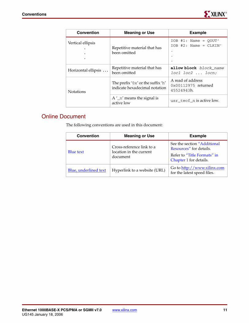
Online DocumentThe following conventions are used in this document:
Vertical ellipsis...
Repetitive material that has been omitted
IOB #1: Name = QOUT’ IOB #2: Name = CLKIN’...
Horizontal ellipsis . . . Repetitive material that has been omitted
allow block block_name loc1 loc2 ... locn;
Notations
The prefix ‘0x’ or the suffix ‘h’ indicate hexadecimal notation
A read of address 0x00112975 returned 45524943h.
A ‘_n’ means the signal is active low usr_teof_n is active low.
Convention Meaning or Use Example
Convention Meaning or Use Example
Blue textCross-reference link to a location in the current document
See the section “Additional Resources” for details.
Refer to “Title Formats” in Chapter 1 for details.
Blue, underlined text Hyperlink to a website (URL) Go to http://www.xilinx.com for the latest speed files.
12 www.xilinx.com Ethernet 1000BASE-X PCS/PMA or SGMII v7.0UG145 January 18, 2006
Preface: About This GuideR
Ethernet 1000BASE-X PCS/PMA or SGMII v7.0 www.xilinx.com 13UG145 January 18, 2006
R
Chapter 1
Introduction
The Ethernet 1000BASE-X PCS/PMA or SGMII core is a fully-verified solution that supports Verilog-HDL and VHDL. In addition, the example design in this guide is provided in both Verilog and VHDL formats.
This chapter introduces the core and provides some related information, including recommended design experience, additional resources, technical support, and how to submit feedback to Xilinx.
About the CoreThe Ethernet 1000BASE-X PCS/PMA or SGMII core is a Xilinx CORE Generator™ IP core, included in the latest IP Update on the Xilinx IP Center. For detailed information about the core, see http://www.xilinx.com/systemio/1gbsx_phy/index.htm. For information about system requirements, installation, and licensing options, see Chapter 2, “Installing and Licensing the Core.”
Recommended Design ExperienceAlthough the Ethernet 1000BASE-X PCS/PMA or SGMII core is a fully-verified solution, the challenge associated with implementing a complete design varies, depending on the configuration and functionality of the application. For best results, previous experience building high-performance, pipelined FPGA designs using Xilinx implementation software and user constraint files (UCFs) is recommended.
Contact your local Xilinx representative for a closer review and estimation for your specific requirements.
Additional Core ResourcesFor detailed information and updates about the Ethernet 1000BASE-X PCS/PMA or SGMII core, see the following documents, located on the Ethernet 1000BASE-X PCS/PMA or SGMII product page at http://www.xilinx.com/systemio/1gbsx_phy/index.htm.
• Xilinx Ethernet 1000BASE-X PCS/PMA or SGMII Data Sheet
• Xilinx Ethernet 1000BASE-X PCS/PMA or SGMII Release Notes
• Xilinx Ethernet 1000BASE-X PCS/PMA or SGMII User Guide
For updates to this document, see the Ethernet 1000BASE-X PCS/PMA or SGMII Getting Started Guide, also located on the Ethernet 1000BASE-X PCS/PMA or SGMII product page.

14 www.xilinx.com Ethernet 1000BASE-X PCS/PMA or SGMII v7.0UG145 January 18, 2006
Chapter 1: IntroductionR
Technical SupportFor technical support, see http://support.xilinx.com/. Questions are routed to a team of engineers with expertise using the Ethernet 1000BASE-X PCS/PMA or SGMII core.
Xilinx will provide technical support for use of this product as described in the Xilinx Ethernet 1000BASE-X PCS/PMA or the Xilinx SGMII User Guide and the Ethernet 1000BASE-X PCS/PMA or SGMII Getting Started Guide. Xilinx cannot guarantee timing, functionality, or support of this product for designs that do not follow these guidelines.
FeedbackXilinx welcomes comments and suggestions about the Ethernet 1000BASE-X PCS/PMA or SGMII core and the documentation supplied with the core.
Ethernet 1000BASE-X PCS/PMA or SGMII CoreFor comments or suggestions about the Ethernet 1000BASE-X PCS/PMA or SGMII core, please submit a WebCase from www.xilinx.com/support/clearexpress/websupport.htm/
Be sure to include the following information:
• Product name
• Core version number
• Explanation of your comments
DocumentFor comments or suggestions about this document, please submit a WebCase from www.xilinx.com/support/clearexpress/websupport.htm/
Be sure to include the following information:
• Document title
• Document number
• Page number(s) to which your comments refer
• Explanation of your comments

Ethernet 1000BASE-X PCS/PMA or SGMII v7.0 www.xilinx.com 15UG145 January 18, 2006
R
Chapter 2
Installing and Licensing the Core
This chapter provides instructions for installing the Ethernet 1000BASE-X PCS/PMA or SGMII core and obtaining a license for the core, which you must do before using the core in your designs. The Ethernet 1000BASE-X PCS/PMA or SGMII core is provided under the terms of the Xilinx LogiCORE Site License Agreement, which conforms to the terms of the SignOnce IP License standard defined by the Common License Consortium.
System Requirements
Windows
• Windows® 2000 Professional with Service Pack 2-4
• Windows XP Professional with Service Pack 1
Solaris/Linux
• Sun Solaris® 8/9
• Red Hat® Enterprise Linux 3.0 (32-bit and 64-bit)
Software
• Xilinx ISETM 8.1i
Before You BeginBefore installing the core, you must have a Xilinx.com account and the ISE 8.1i software installed on your system. If you have already completed these steps, go to “Installing the Core.”
1. Click Login at the top of the Xilinx home page; then follow the onscreen instructions to create a support account.
2. Install the ISE 8.1i software and the applicable Service Pack software. ISE Service Packs can be downloaded from www.xilinx.com/support/download.htm.
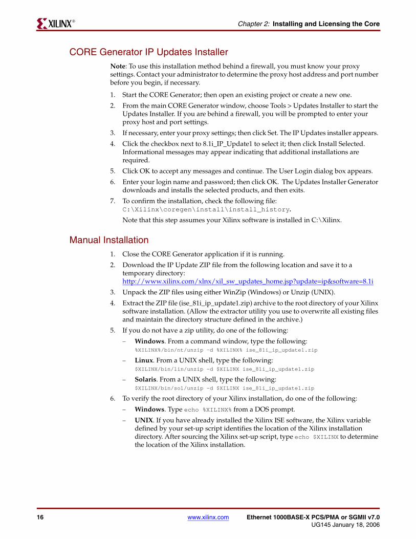
Installing the CoreYou can install the core in two ways—using the CORE Generator IP Updates Installer, which lets you select from a list of updates—or by performing a manual installation after downloading the core from the web.
16 www.xilinx.com Ethernet 1000BASE-X PCS/PMA or SGMII v7.0UG145 January 18, 2006
Chapter 2: Installing and Licensing the CoreR
CORE Generator IP Updates InstallerNote: To use this installation method behind a firewall, you must know your proxy settings. Contact your administrator to determine the proxy host address and port number before you begin, if necessary.
1. Start the CORE Generator; then open an existing project or create a new one.
2. From the main CORE Generator window, choose Tools > Updates Installer to start the Updates Installer. If you are behind a firewall, you will be prompted to enter your proxy host and port settings.
3. If necessary, enter your proxy settings; then click Set. The IP Updates installer appears.
4. Click the checkbox next to 8.1i_IP_Update1 to select it; then click Install Selected. Informational messages may appear indicating that additional installations are required.
5. Click OK to accept any messages and continue. The User Login dialog box appears.
6. Enter your login name and password; then click OK. The Updates Installer Generator downloads and installs the selected products, and then exits.
7. To confirm the installation, check the following file: C:\Xilinx\coregen\install\install_history. Note that this step assumes your Xilinx software is installed in C:\Xilinx.
Manual Installation1. Close the CORE Generator application if it is running.
2. Download the IP Update ZIP file from the following location and save it to a temporary directory: http://www.xilinx.com/xlnx/xil_sw_updates_home.jsp?update=ip&software=8.1i
3. Unpack the ZIP files using either WinZip (Windows) or Unzip (UNIX).
4. Extract the ZIP file (ise_81i_ip_update1.zip) archive to the root directory of your Xilinx software installation. (Allow the extractor utility you use to overwrite all existing files and maintain the directory structure defined in the archive.)
5. If you do not have a zip utility, do one of the following:
− Windows. From a command window, type the following:%XILINX%/bin/nt/unzip -d %XILINX% ise_81i_ip_update1.zip
− Linux. From a UNIX shell, type the following: $XILINX/bin/lin/unzip -d $XILINX ise_81i_ip_update1.zip
− Solaris. From a UNIX shell, type the following: $XILINX/bin/sol/unzip -d $XILINX ise_81i_ip_update1.zip
6. To verify the root directory of your Xilinx installation, do one of the following:
− Windows. Type echo %XILINX% from a DOS prompt.
− UNIX. If you have already installed the Xilinx ISE software, the Xilinx variable defined by your set-up script identifies the location of the Xilinx installation directory. After sourcing the Xilinx set-up script, type echo $XILINX to determine the location of the Xilinx installation.

Ethernet 1000BASE-X PCS/PMA or SGMII v7.0 www.xilinx.com 17UG145 January 18, 2006
Verifying the InstallationR
Verifying the Installation1. Start the CORE Generator.
2. After creating a new project or opening an existing one, the IP core functional categories appear at the left side of the window.
3. Click to expand or collapse the view of individual functional categories, or click the View by Name tab at the bottom of the list to see an alphabetical list of all cores in all categories.
4. To view specific versions of the cores, choose an option from the Show drop-down list at the top of the window:
− Latest Versions. Display the latest versions of all cores.
− All Versions. Display all versions of cores, including new cores and new versions of cores.
− All Versions including Obsolete. Display all cores, including those scheduled to become obsolete.
5. Determine if the installation was successful by verifying that the new core or cores appear in the CORE Generator GUI.
For additional assistance installing the IP Update, contact www.xilinx.com/support.
License OptionsThe Ethernet 1000BASE-X PCS/PMA or SGMII core has the following two licensing options.
Figure 2-1: CORE Generator Window
FunctionalCategories
Viewing Options
View by Name
18 www.xilinx.com Ethernet 1000BASE-X PCS/PMA or SGMII v7.0UG145 January 18, 2006
Chapter 2: Installing and Licensing the CoreR
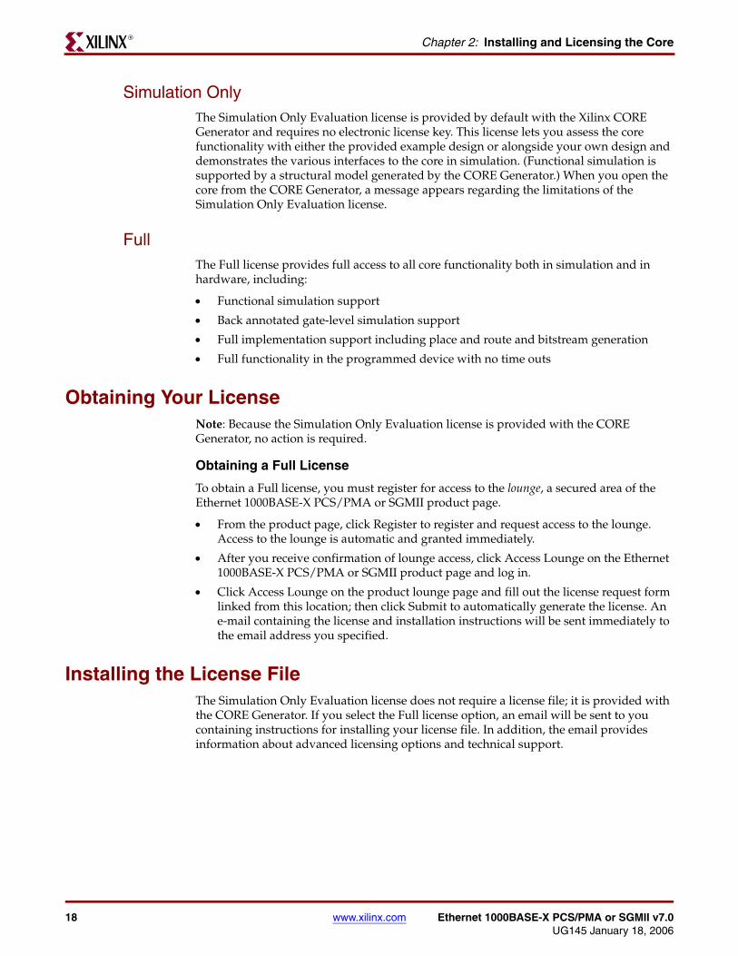
Simulation Only The Simulation Only Evaluation license is provided by default with the Xilinx CORE Generator and requires no electronic license key. This license lets you assess the core functionality with either the provided example design or alongside your own design and demonstrates the various interfaces to the core in simulation. (Functional simulation is supported by a structural model generated by the CORE Generator.) When you open the core from the CORE Generator, a message appears regarding the limitations of the Simulation Only Evaluation license.
Full The Full license provides full access to all core functionality both in simulation and in hardware, including:
• Functional simulation support
• Back annotated gate-level simulation support
• Full implementation support including place and route and bitstream generation
• Full functionality in the programmed device with no time outs
Obtaining Your LicenseNote: Because the Simulation Only Evaluation license is provided with the CORE Generator, no action is required.
Obtaining a Full License
To obtain a Full license, you must register for access to the lounge, a secured area of the Ethernet 1000BASE-X PCS/PMA or SGMII product page.
• From the product page, click Register to register and request access to the lounge. Access to the lounge is automatic and granted immediately.
• After you receive confirmation of lounge access, click Access Lounge on the Ethernet 1000BASE-X PCS/PMA or SGMII product page and log in.
• Click Access Lounge on the product lounge page and fill out the license request form linked from this location; then click Submit to automatically generate the license. An e-mail containing the license and installation instructions will be sent immediately to the email address you specified.
Installing the License FileThe Simulation Only Evaluation license does not require a license file; it is provided with the CORE Generator. If you select the Full license option, an email will be sent to you containing instructions for installing your license file. In addition, the email provides information about advanced licensing options and technical support.
Ethernet 1000BASE-X PCS/PMA or SGMII v7.0 www.xilinx.com 19UG145 January 18, 2006
R
Chapter 3
Quick Start Example Design
The quick start steps provided in this chapter let you quickly generate an Ethernet 1000BASE-X PCS/PMA or SGMII core, run the design through implementation with the Xilinx tools, and simulate the design using the provided demonstration test bench. For detailed information about the example design, see Chapter 4, “Detailed Example Design.”
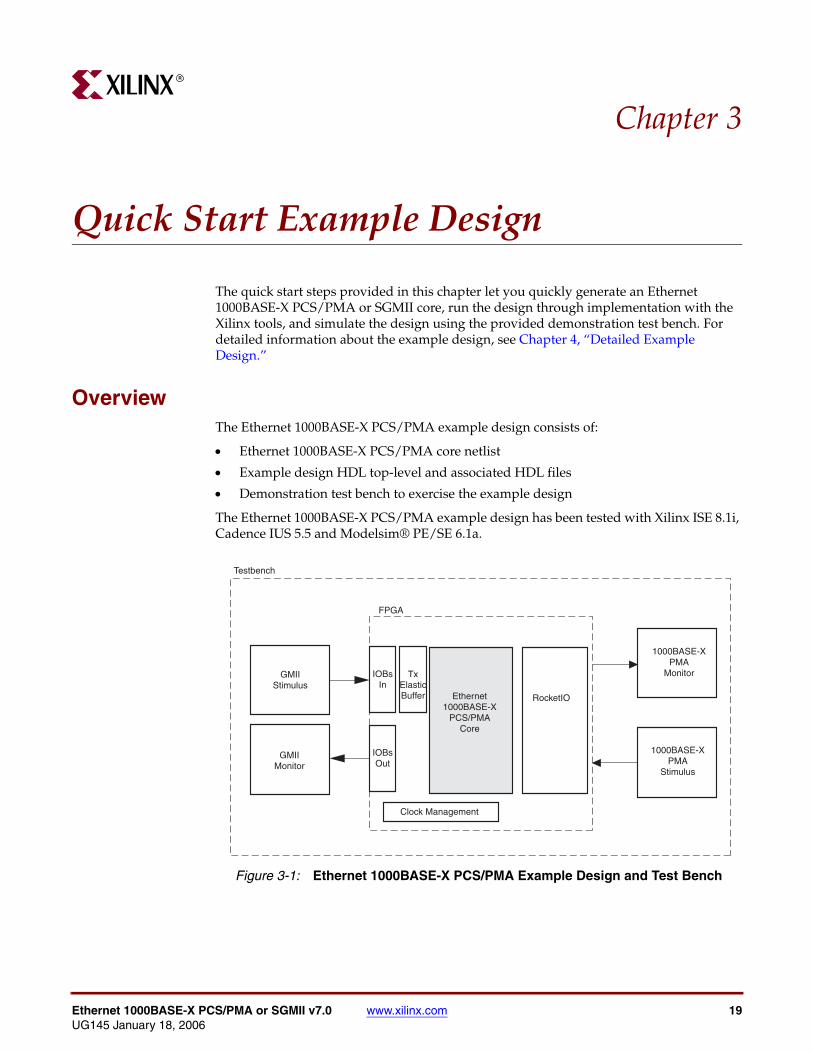
OverviewThe Ethernet 1000BASE-X PCS/PMA example design consists of:
• Ethernet 1000BASE-X PCS/PMA core netlist
• Example design HDL top-level and associated HDL files
• Demonstration test bench to exercise the example design
The Ethernet 1000BASE-X PCS/PMA example design has been tested with Xilinx ISE 8.1i, Cadence IUS 5.5 and Modelsim® PE/SE 6.1a.
Figure 3-1: Ethernet 1000BASE-X PCS/PMA Example Design and Test Bench
1000BASE-XPMA
Monitor
1000BASE-XPMA
Stimulus
GMIIStimulus
GMIIMonitor
IOBsIn
IOBsOut
Ethernet1000BASE-X
PCS/PMACore
Clock Management
FPGA
Testbench
RocketIO
TxElasticBuffer
20 www.xilinx.com Ethernet 1000BASE-X PCS/PMA or SGMII v7.0UG145 January 18, 2006
Chapter 3: Quick Start Example DesignR
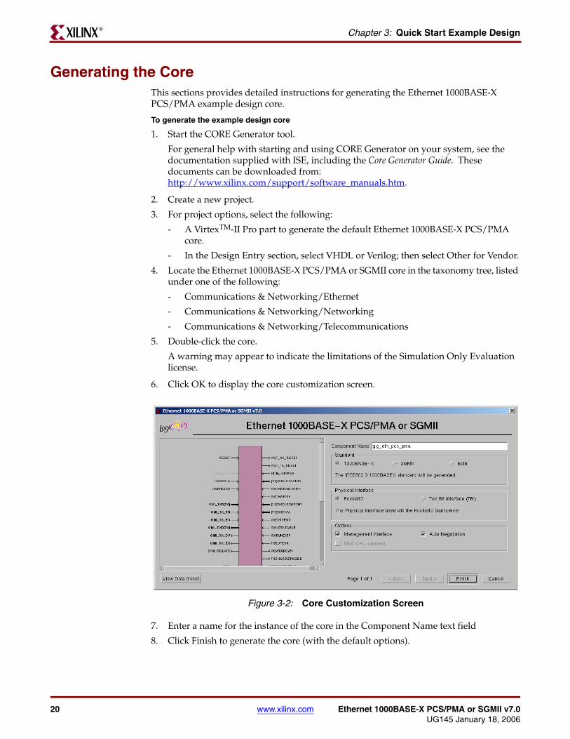
Generating the CoreThis sections provides detailed instructions for generating the Ethernet 1000BASE-X PCS/PMA example design core.
To generate the example design core
1. Start the CORE Generator tool.
For general help with starting and using CORE Generator on your system, see the documentation supplied with ISE, including the Core Generator Guide. These documents can be downloaded from: http://www.xilinx.com/support/software_manuals.htm.
2. Create a new project.
3. For project options, select the following:
- A VirtexTM-II Pro part to generate the default Ethernet 1000BASE-X PCS/PMA core.
- In the Design Entry section, select VHDL or Verilog; then select Other for Vendor.
4. Locate the Ethernet 1000BASE-X PCS/PMA or SGMII core in the taxonomy tree, listed under one of the following:
- Communications & Networking/Ethernet
- Communications & Networking/Networking
- Communications & Networking/Telecommunications
5. Double-click the core.
A warning may appear to indicate the limitations of the Simulation Only Evaluation license.
6. Click OK to display the core customization screen.
7. Enter a name for the instance of the core in the Component Name text field
8. Click Finish to generate the core (with the default options).
Figure 3-2: Core Customization Screen
Ethernet 1000BASE-X PCS/PMA or SGMII v7.0 www.xilinx.com 21UG145 January 18, 2006
Implementing the Example DesignR
The default core and its supporting files, including the example design, are generated in your project directly. For a detailed description of the design example files and directories, refer to “Directory Structure and File Descriptions” in Chapter 4.
Implementing the Example DesignNote: Available only with a Full license.
After the core is generated, the netlists and example design can be processed by the Xilinx implementation tools. The generated output files include several scripts to assist you in running the Xilinx software.
To implement the Ethernet 1000BASE-X PCS/PMA or SGMII sample design core
From the CORE Generator project directory window, type in the following:
For UNIX:
unix-shell> cd <project_dir>/<component_name>/implement
unix-shell> ./implement.sh
For Windows:
ms-dos> cd <project_dir>\<component_name>\implement
ms-dos> implement.bat
These commands execute a script that synthesizes, builds, maps, and place-and-routes the example design. The script then creates gate-level netlist HDL files in either VHDL or Verilog, along with associated timing information (SDF) files.
Simulating the Example Design
Setting up for SimulationTo run the gate-level simulation you must have the Xilinx Simulation Libraries compiled for your system. See the Compiling Xilinx Simulation Libraries (COMPXLIB) in the Xilinx ISE Synthesis and Verification Design Guide, and the Xilinx ISE Software Manuals and Help. You can download these documents from: http://www.xilinx.com/support/software_manuals.htm.
In addition, the simulator you use must provide SWIFT model support to simulate the Virtex-II Pro or Virtex-4 RocketIOTM transceivers.
In the simulation examples that follow, <project_dir> is the CORE Generator project directory; <component_name> is the component name as entered in the core customization window.
Functional SimulationNote: Available for both license types.
This section provides instructions for running a functional simulation or the Ethernet 1000BASE-X PCS/PMA or SGMII core using either VHDL or Verilog. The functional simulation model is provided when the core generated; implementing the core before simulation is not required.
22 www.xilinx.com Ethernet 1000BASE-X PCS/PMA or SGMII v7.0UG145 January 18, 2006
Chapter 3: Quick Start Example DesignR
To run a VHDL or Verilog functional simulation of the example design:
1. Open a command prompt or shell, then set the current directory to: <project_dir>/<component_name>/simulation/functional/
2. Launch the simulation script:
ModelSim: vsim -do simulate_mti.do
IUS: ./simulate_ncsim.sh
The simulation script compiles the functional simulation model, the example design files, the demonstration test bench, and adds relevant signals to a wave window. It then runs the simulation to completion. After completion, you can inspect the simulation transcript and waveform to observe the operation of the core.
Timing SimulationNote: Available only with a Full license.
This section contains instructions for running a timing simulation or the Ethernet 1000BASE-X PCS/PMA or SGMII core using either VHDL or Verilog. A timing simulation model is generated when run through the Xilinx tools using the implementation script. You must implement the core before attempting to run timing simulation.
To run a VHDL or Verilog timing simulation of the example design:
1. Run the implementation script (see “Implementing the Example Design”).
2. Open a command prompt or shell, then set the current directory to: <project_dir>/<component_name>/simulation/timing/
3. Launch the simulation script:
ModelSim: vsim -do simulate_mti.do
IUS: ./simulate_ncsim.sh
The simulator script compiles the gate-level model and the demonstration test bench, adds relevant signals to a wave window, and then runs the simulation to completion. You can then inspect the simulation transcript and waveform to observe the operation of the core.
What’s Next?For detailed information about the example design, including guidelines for modifying the design and extending the test bench, see Chapter 4, “Detailed Example Design.”
To begin using the Ethernet 1000BASE-X PCS/PMA or SGMII core in your own designs, see the Xilinx Ethernet 1000BASE-X PCS/PMA or SGMII User Guide.

Ethernet 1000BASE-X PCS/PMA or SGMII v7.0 www.xilinx.com 23UG145 January 18, 2006
R
Chapter 4
Detailed Example Design
This chapter provides detailed information about the Ethernet 1000BASE-X PCS/PMA or SGMII example design, including a description of files and the directory structure generated by the Xilinx CORE Generator, the purpose and contents of the provided scripts, the contents of the example HDL wrappers, and the demonstration test bench.
Directory Structure and File Descriptions
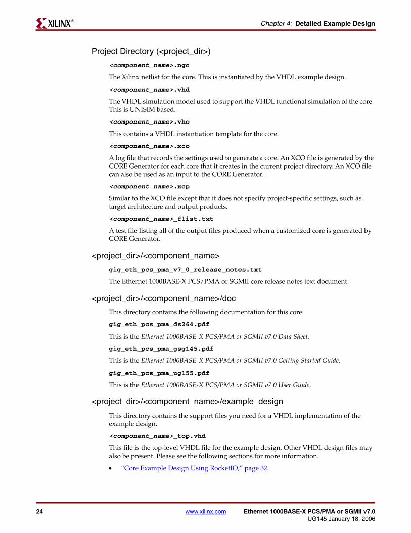
VHDL Design EntryFigure 4-1 shows the files and directories created by CORE Generator system in a VHDL Design Entry Project. In this example, <project_dir> is the CORE Generator project directory; <component_name> is the component name as entered in the core customization window.
Note: The implement and simulation/timing directories are only present with a Full license.
Figure 4-1: Core Directories and Files
<project_dir>
<component_name>
<component_name>.ngc<component_name>.vhd<component_name>.vho<component_name>.xco<component_name>.xcp<component_name>_flist.txt
doc
example_design<component_name>_top.vhd<component_name>_top.ucfOther Example Design VHDLfiles
implementimplement.batimplement.shxst.scrxst.prj results
Generated by the implement scriptsContains the back-annotated vhdl netlist files.
simulation
functional
timing
simulate_mti.dowave_mti.dosimulate_ncsim.shwave_ncsim.svdemo_tb.vhd
gig_eth_pcs_pma_v7_0_release_notes.txt
gig_eth_pcs_pma_ds264.pdfgig_eth_pcs_pma_gsg145.pdfgig_eth_pcs_pma_ug155.pdf
simulate_mti.dowave_mti.dosimulate_ncsim.shwave_ncsim.sv
24 www.xilinx.com Ethernet 1000BASE-X PCS/PMA or SGMII v7.0UG145 January 18, 2006
Chapter 4: Detailed Example DesignR
Project Directory (<project_dir>)
<component_name>.ngc
The Xilinx netlist for the core. This is instantiated by the VHDL example design.
<component_name>.vhd
The VHDL simulation model used to support the VHDL functional simulation of the core. This is UNISIM based.
<component_name>.vho
This contains a VHDL instantiation template for the core.
<component_name>.xco
A log file that records the settings used to generate a core. An XCO file is generated by the CORE Generator for each core that it creates in the current project directory. An XCO file can also be used as an input to the CORE Generator.
<component_name>.xcp
Similar to the XCO file except that it does not specify project-specific settings, such as target architecture and output products.
<component_name>_flist.txt
A test file listing all of the output files produced when a customized core is generated by CORE Generator.
<project_dir>/<component_name>
gig_eth_pcs_pma_v7_0_release_notes.txt
The Ethernet 1000BASE-X PCS/PMA or SGMII core release notes text document.
<project_dir>/<component_name>/doc
This directory contains the following documentation for this core.
gig_eth_pcs_pma_ds264.pdf
This is the Ethernet 1000BASE-X PCS/PMA or SGMII v7.0 Data Sheet.
gig_eth_pcs_pma_gsg145.pdf
This is the Ethernet 1000BASE-X PCS/PMA or SGMII v7.0 Getting Started Guide.
gig_eth_pcs_pma_ug155.pdf
This is the Ethernet 1000BASE-X PCS/PMA or SGMII v7.0 User Guide.
<project_dir>/<component_name>/example_design
This directory contains the support files you need for a VHDL implementation of the example design.
<component_name>_top.vhd
This file is the top-level VHDL file for the example design. Other VHDL design files may also be present. Please see the following sections for more information.
• “Core Example Design Using RocketIO,” page 32.

Ethernet 1000BASE-X PCS/PMA or SGMII v7.0 www.xilinx.com 25UG145 January 18, 2006
Directory Structure and File DescriptionsR
• “Core Example Design with Ten-Bit Interface,” page 36.
• “SGMII Example Design / Dynamic Switching Example Design,” page 40.
<project_dir>/implement
Note: This directory is only present with the Full license.
implement.sh
A UNIX shell script that processes the example design through the Xilinx tool flow. See “Implementation Scripts,” page 30 for more information.
implement.bat
A Windows batch file that process the example design through the Xilinx tool flow. See “Implementation Scripts,” page 30 for more information.
xst.prj
The XST project file for the example design; it enumerates all of the VHDL files that need to be synthesized.
xst.scr
The XST script file for the example design.
<project_dir>/implement/results
This directory is produced by the implementation scripts and is used to run through the example design and the core through the Xilinx implementation tools. Once the implement script has completed it contains the following files for timing simulation.
routed.vhd
The back-annotated simprim based VHDL model used for timing simulation. This is SIMPRIM-based.
routed.sdf
The timing information for simulation is contained in this file.
<project_dir>/<component_name>/simulation
The simulation directory and subdirectories that provide the files necessary to test a VHDL implementation of the example design.
demo_tb.vhd
The VHDL demonstration test bench file for the example design. See the following for more information.
• “Core Example Design Using RocketIO,” page 32.
• “Core Example Design with Ten-Bit Interface,” page 36.
• “SGMII Example Design / Dynamic Switching Example Design,” page 40.
<project_dir>/<component_name>/simulation/functional
simulate_mti.do
A ModelSim® macro file that compiles the VHDL sources and then runs the functional simulation to completion.
26 www.xilinx.com Ethernet 1000BASE-X PCS/PMA or SGMII v7.0UG145 January 18, 2006
Chapter 4: Detailed Example DesignR
wave_mti.do
A ModelSim macro file that opens a wave window and adds signals of interest to it. It is called by the simulate_mti.do macro file.
simulate_ncsim.sh
An IUS script file that compiles the VHDL sources and then runs the functional simulation to completion.
wave_ncsim.sv
An IUS macro file that opens a wave window and adds signals of interest to it. It is called by the simulate_ncsim.sh script file.
<project_dir>/<component_name>/simulation/timing
Note: This directory is only present with the Full license.
simulate_mti.do
A ModelSim macro file that compiles the VHDL sources and then runs the timing simulation to completion.
wave_mti.do
A ModelSim macro file that opens a wave window and adds signals of interest to it. It is called by the simulate_mti.do macro file.
simulate_ncsim.sh
An IUS script file that compiles the VHDL sources and then runs the timing simulation to completion.
wave_ncsim.sv
An IUS macro file that opens a wave window and adds signals of interest to it. It is called by the simulate_ncsim.sh script file.
Ethernet 1000BASE-X PCS/PMA or SGMII v7.0 www.xilinx.com 27UG145 January 18, 2006
Directory Structure and File DescriptionsR
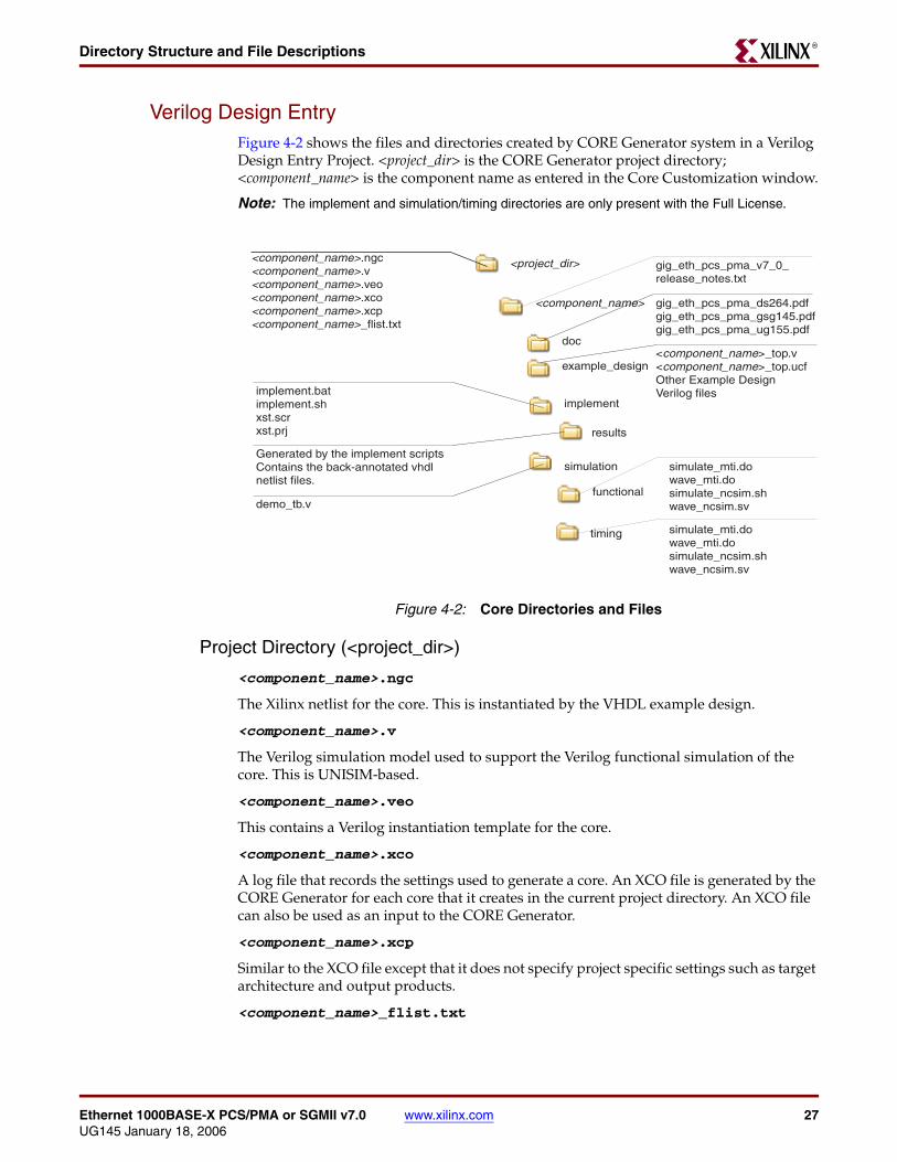
Verilog Design EntryFigure 4-2 shows the files and directories created by CORE Generator system in a Verilog Design Entry Project. <project_dir> is the CORE Generator project directory; <component_name> is the component name as entered in the Core Customization window.
Note: The implement and simulation/timing directories are only present with the Full License.
Project Directory (<project_dir>)
<component_name>.ngc
The Xilinx netlist for the core. This is instantiated by the VHDL example design.
<component_name>.v
The Verilog simulation model used to support the Verilog functional simulation of the core. This is UNISIM-based.
<component_name>.veo
This contains a Verilog instantiation template for the core.
<component_name>.xco
A log file that records the settings used to generate a core. An XCO file is generated by the CORE Generator for each core that it creates in the current project directory. An XCO file can also be used as an input to the CORE Generator.
<component_name>.xcp
Similar to the XCO file except that it does not specify project specific settings such as target architecture and output products.
<component_name>_flist.txt
Figure 4-2: Core Directories and Files
<project_dir>
<component_name>
<component_name>.ngc<component_name>.v<component_name>.veo<component_name>.xco<component_name>.xcp<component_name>_flist.txt
doc
example_design<component_name>_top.v<component_name>_top.ucfOther Example DesignVerilog files
implementimplement.batimplement.shxst.scrxst.prj results
Generated by the implement scriptsContains the back-annotated vhdl netlist files.
simulation
functional
timing
demo_tb.v
gig_eth_pcs_pma_v7_0_release_notes.txt
gig_eth_pcs_pma_ds264.pdfgig_eth_pcs_pma_gsg145.pdfgig_eth_pcs_pma_ug155.pdf
simulate_mti.dowave_mti.dosimulate_ncsim.shwave_ncsim.sv
simulate_mti.dowave_mti.dosimulate_ncsim.shwave_ncsim.sv
28 www.xilinx.com Ethernet 1000BASE-X PCS/PMA or SGMII v7.0UG145 January 18, 2006
Chapter 4: Detailed Example DesignR
A test file listing all of the output files produced when a customized core is generated by CORE Generator.
<project_dir>/<component_name>
gig_eth_pcs_pma_v7_0_release_notes.txt
The Ethernet 1000BASE-X PCS/PMA or SGMII core release notes text document.
<project_dir>/<component_name>/doc
This directory contains documentation for the core.
gig_eth_pcs_pma_ds264.pdf
This is the Xilinx Ethernet 1000BASE-X PCS/PMA or SGMII v7.0 Data Sheet.
gig_eth_pcs_pma_gsg145.pdf
This is the Xilinx Ethernet 1000BASE-X PCS/PMA or SGMII v7.0 Getting Started Guide.
gig_eth_pcs_pma_ug155.pdf
This is the Xilinx Ethernet 1000BASE-X PCS/PMA or SGMII v7.0 User Guide.
<project_dir>/<component_name>/example_design
This directory contains the support files necessary for a Verilog implementation of the example design.
<component_name>_top.v
This file is the top-level Verilog file for the example design. Other Verilog design files may also be present. Please see the following for more information.
• “Core Example Design Using RocketIO,” page 32
• “Core Example Design with Ten-Bit Interface,” page 36
• “SGMII Example Design / Dynamic Switching Example Design,” page 40
<project_dir>/implement
Note: This directory is only present with the Full license.
implement.sh
A UNIX shell script that processes the example design through the Xilinx tool flow. See “Implementation Scripts,” page 30 for more information.
implement.bat
A Windows batch file that process the example design through the Xilinx tool flow. See “Implementation Scripts,” page 30 for more information.
xst.prj
The XST project file for the example design. It enumerates all of the Verilog files that need to be synthesized.
xst.scr
The XST script file for the example design.
Ethernet 1000BASE-X PCS/PMA or SGMII v7.0 www.xilinx.com 29UG145 January 18, 2006
Directory Structure and File DescriptionsR
<project_dir>/implement/results
This directory is produced by the implementation scripts and is used to run through the example design and the core through the Xilinx implementation tools. Once the implement script has completed it contains the following files for timing simulation.
routed.v
The back-annotated simprim based Verilog model used for timing simulation. This is SimPrim-based.
routed.sdf
The timing information for simulation is contained in this file.
<project_dir>/<component_name>/simulation
The simulation directory and subdirectories provide the files you need to test a Verilog implementation of the example design.
demo_tb.v
The Verilog demonstration test bench file for the example design. See the following sections in this document for more information.
• “Core Example Design Using RocketIO,” page 32
• “Core Example Design with Ten-Bit Interface,” page 36
• “SGMII Example Design / Dynamic Switching Example Design,” page 40
<project_dir>/<component_name>/simulation/functional
simulate_mti.do
A ModelSim macro file that compiles the Verilog sources and then runs the functional simulation to completion.
wave_mti.do
A ModelSim macro file that opens a wave window and adds signals of interest to it. It is called by the simulate_mti.do macro file.
simulate_ncsim.sh
An IUS script file that compiles the Verilog sources and runs the functional simulation to completion.
wave_ncsim.sv
An IUS macro file that opens a wave window and adds signals of interest to it. It is called by the simulate_ncsim.sh script file.
<project_dir>/<component_name>/simulation/timing
Note: This directory is only present with the Full license.
simulate_mti.do
A ModelSim macro file that compiles the Verilog sources and then runs the timing simulation to completion.
wave_mti.do
30 www.xilinx.com Ethernet 1000BASE-X PCS/PMA or SGMII v7.0UG145 January 18, 2006
Chapter 4: Detailed Example DesignR
A ModelSim macro file that opens a wave window and adds signals of interest to it. It is called by the simulate_mti.do macro file.
simulate_ncsim.sh
An IUS script file that compiles the Verilog sources and then runs the timing simulation to completion.
wave_ncsim.sv
An IUS macro file that opens a wave window and adds signals of interest to it. It is called by the simulate_ncsim.sh script file.
Implementation ScriptsNote: These scripts are only present with the Full license.
The implementation script is either a shell script or batch file that processes the example design through the Xilinx tool flow. It is located at:
UNIX:
<project_dir>/<component_name>/implement/implement.sh
Windows:
<project_dir>/<component_name>/implement/implement.bat
The implement script performs the following steps:
1. The HDL example design files are synthesized using XST.
2. Ngdbuild is run to consolidate the core netlist and the example design netlist into the NGD file containing the entire design.
3. The design is mapped to the target technology.
4. The design is placed-and-routed on the target device.
5. Static timing analysis is performed on the routed design using trce.
6. A bitstream is generated.
7. Netgen runs on the routed design to generate a VHDL or Verilog netlist (as appropriate for the Design Entry project setting) and timing information in the form of SDF files.
The Xilinx tool flow generates several output and report files. These are saved in the following directory which is created by the implement script:
<project_dir>/<component_name>/implement/results
Simulation Scripts
Functional simulationThe test script is a ModelSim or an IUS macro that automates the simulation of the test bench. It is located at:
<project_dir>/<component_name>/simulation/functional/
The test script performs the following tasks:
• Compiles the structural UNISIM simulation model
Ethernet 1000BASE-X PCS/PMA or SGMII v7.0 www.xilinx.com 31UG145 January 18, 2006
Simulation ScriptsR
• Compiles HDL example design source code
• Compiles the demonstration test bench
• Starts a simulation of the test bench
• Opens a Wave window and adds signals of interest (wave_mti.do/wave_ncsim.sv)
• Runs the simulation to completion
Timing simulationNote: This script is only present with the Full license.
The test script is a ModelSim or an IUS macro that automates the simulation of the test bench. It is located at:
<project_dir>/<component_name>/simulation/timing/
The test script performs the following tasks.
• Compiles the SimPrim based gate level netlist simulation model
• Compiles the demonstration test bench
• Starts a simulation of the test bench
• Opens a Wave window and adds signals of interest (wave_mti.do/wave_ncsim.sv)
• Runs the simulation to completion

32 www.xilinx.com Ethernet 1000BASE-X PCS/PMA or SGMII v7.0UG145 January 18, 2006
Chapter 4: Detailed Example DesignR
Core Example Design Using RocketIO
Top-Level HDLFigure 4-3 illustrates the example design for a top-level HDL for the Ethernet 1000BASE-X PCS/PMA using RocketIO.
The following files describe the top-level example design for the Ethernet 1000BASE-X PCS/PMA core using a RocketIO core.
VHDL
project_dir>/<component_name>/example_design/<component_name>_top.vhd
Verilog
project_dir>/<component_name>/example_design/<component_name>_top.v
The example design HDL top level contains the following:
• An instance of the Ethernet 1000BASE-X PCS/PMA core
• An instance of a Virtex-II Pro or Virtex-4 RocketIO transceiver
• Clock management logic for the core and the RocketIO transceiver, including DCM and Global Clock Buffer instances
• A transmitter elastic buffer
• GMII interface logic, including IOB and DDR registers instances, where required
• Input and output buffers for other port signals of the top level
Figure 4-3: Top-Level HDL for the Ethernet 1000BASE-X PCS/PMA using RocketIO
Ethernet1000BASE-X
PCS/PMACore
Clock Management
FPGA
RocketIO
TransceiverGMII
IOBsIn
IOBsOut
Connect toClient MAC
PMA (Connect to
Optical Transceiver)
TxElasticBuffer

Ethernet 1000BASE-X PCS/PMA or SGMII v7.0 www.xilinx.com 33UG145 January 18, 2006
Core Example Design Using RocketIOR
The example design HDL top-level connects the GMII of the core to external IOBs and the PHY side interface of the core directly to a RocketIO instance. This configuration allows the functionality of the core to be demonstrated using a simulation package as discussed in this guide. The example design can also be synthesized and, if required, placed on a suitable board and demonstrated in hardware.
TransceiverA wrapper file for the Virtex-II Pro RocketIO or Virtex-4 Multi-Gigabit Transceiver is described in the following files:
VHDL
project_dir>/<component_name>/example_design/transceiver.vhd
Verilog
project_dir>/<component_name>/example_design/transceiver.v
This file instances a Virtex-II Pro RocketIO or Virtex-4 RocketIO and applies Gigabit Ethernet 1000BASE-X attributes to it. This transceiver wrapper is instantiated from the top-level HDL file for the example design.
For Virtex-4 FX devices only, a Calibration Block is required. See the Calibration Block Users Guide for more information.
This is decribed in the following files: VHDL
project_dir/<component_name>/example_design/cal_block_v1_2_1.vhd
Verilog
project_dir/<component_name>/example_design/cal_block_v1_2_1.v
Transmitter Elastic BufferThe Transmitter Elastic Buffer is described in the following files:
VHDL
project_dir>/<component_name>/example_design/tx_elastic_buffer.vhd
Verilog
project_dir>/<component_name>/example_design/tx_elastic_buffer.v
When the GMII is used externally (as in this example design), the GMII transmit signals (inputs to the core from a remote MAC at the other end of the interface) are synchronous to a clock that is likely to be derived from a different clock source to the core. For this reason, GMII transmit signals must be transferred into the core main clock domain before they can be used by the core and RocketIO. This is achieved with the Transmitter Elastic Buffer, an a synchronous FIFO implemented in distributed RAM. The operation of the elastic buffer is to attempt to maintain a constant occupancy by inserting or removing any idle sequences. This causes no corruption to the frames of data.
When the GMII is used as an internal interface, it is expected that the entire interface will be synchronous to a single clock domain and the Transmitter Elastic Buffer should be discarded. See the LogiCORE Ethernet 1000BASE-X PCS/PMA or SGMII User Guide for information about connecting the core to an internal GMII or an Ethernet MAC.
34 www.xilinx.com Ethernet 1000BASE-X PCS/PMA or SGMII v7.0UG145 January 18, 2006
Chapter 4: Detailed Example DesignR
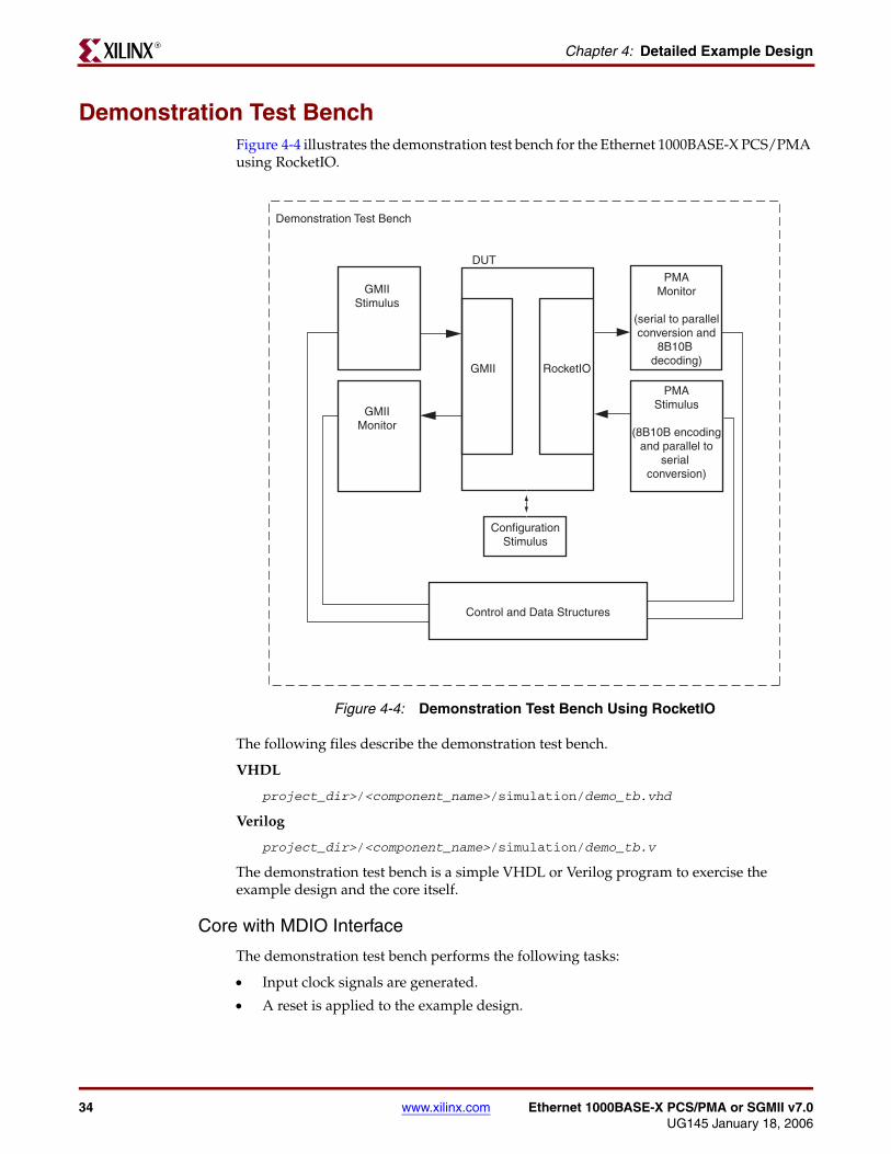
Demonstration Test BenchFigure 4-4 illustrates the demonstration test bench for the Ethernet 1000BASE-X PCS/PMA using RocketIO.
The following files describe the demonstration test bench.
VHDL
project_dir>/<component_name>/simulation/demo_tb.vhd
Verilog
project_dir>/<component_name>/simulation/demo_tb.v
The demonstration test bench is a simple VHDL or Verilog program to exercise the example design and the core itself.
Core with MDIO Interface
The demonstration test bench performs the following tasks:
• Input clock signals are generated.
• A reset is applied to the example design.
Figure 4-4: Demonstration Test Bench Using RocketIO
PMAMonitor
(serial to parallelconversion and
8B10B decoding)
PMAStimulus
(8B10B encodingand parallel to
serial conversion)
GMIIStimulus
GMIIMonitor
GMII RocketIO
DUT
Demonstration Test Bench
Control and Data Structures
ConfigurationStimulus
Ethernet 1000BASE-X PCS/PMA or SGMII v7.0 www.xilinx.com 35UG145 January 18, 2006
Demonstration Test BenchR
• The Ethernet 1000BASE-X PCS/PMA core is configured through the MDIO interface by injecting an MDIO frame into the example design. This disables Auto-Negotiation (if present) and takes the core out of the Isolate state.
• Four frames are injected into the GMII transmitter by the GMII stimulus block.
- the first frame is a minimum length frame
- the second frame is a type frame
- the third frame is an errored frame
- the fourth frame is a padded frame
• The serial data received at the RocketIO transmitter interface is converted to 10-bit parallel data, then 8B10B decoded. The resultant frames are checked by the PMA Monitor against the stimulus frames injected into the GMII transmitter to ensure data integrity.
• The same four frames are generated by the PMA Stimulus block. These are 8B10B encoded, converted to serial data and injected into the RocketIO receiver interface.
• Data frames received at the GMII receiver are checked by the GMII Monitor against the stimulus frames injected into the RocketIO receiver to ensure data integrity.
Core without MDIO Interface
The demonstration test bench performs the following tasks.
• Input clock signals are generated
• A reset is applied to the example design
• The Ethernet 1000BASE-X PCS/PMA core is configured using the Configuration Vector to take the core out of the Isolate state
• Four frames are injected into the GMII transmitter by the GMII stimulus block.
- the first frame is a minimum length frame
- the second frame is a type frame
- the third frame is an errored frame
- the fourth frame is a padded frame
• The serial data received at the RocketIO transmitter interface is converted to 10-bit parallel data, then 8B10B decoded. The resultant frames are checked by the PMA Monitor against the stimulus frames injected into the GMII transmitter to ensure data integrity.
• The same four frames are generated by the PMA Stimulus block. These are 8B10B encoded, converted to serial data and injected into the RocketIO receiver interface.
• Data frames received at the GMII receiver are checked by the GMII Monitor against the stimulus frames injected into the RocketIO receiver to ensure data is the same.
Customizing the Test Bench
Changing Frame Data
You can change the contents of the four frames used by the demonstration test bench by changing the data and valid fields for each frame defined. New frames can be added by defining a new frame of data. Modified frames are automatically updated in both stimulus and monitor functions.
36 www.xilinx.com Ethernet 1000BASE-X PCS/PMA or SGMII v7.0UG145 January 18, 2006
Chapter 4: Detailed Example DesignR
Changing Frame Error Status
Errors can be inserted into any of the predefined frames in any position by setting the “error” field to ‘1’ in any column of that frame. Injected errors are automatically updated in both stimulus and monitor functions.
Changing the Core Configuration
The configuration of the Ethernet 1000BASE-X PCS/PMA core used in the demonstration test bench can be altered.
Caution: Certain configurations of the core will cause the test bench to fail or to cause processes to run indefinitely. For example, the demonstration test bench will not Auto-Negotiate with the example design. You determine the configurations that can safely be used with the test bench.
When the MDIO interface option is selected, the core can be reconfigured by editing the injected MDIO frame in the demonstration test bench. See the Xilinx LogiCORE Ethernet 1000BASE-X PCS/PMA or SGMII User Guide for more information on using the MDIO interface.
When the MDIO interface option is not selected, the core can be reconfigured by modifying the configuration vector directly. See the Xilinx LogiCORE Ethernet 1000BASE-X PCS/PMA or SGMII User Guide for information on using the configuration vector.
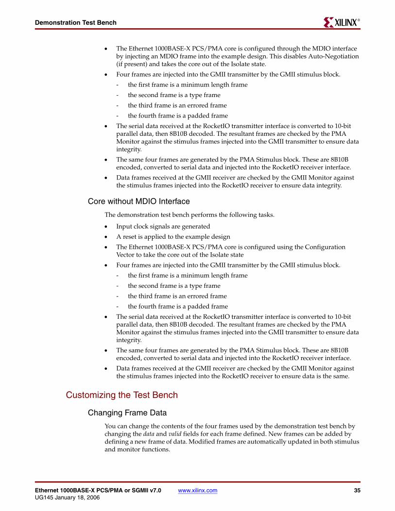
Core Example Design with Ten-Bit Interface
Example Design Top-Level HDLFigure 4-5 illustrates the example design for a top-level HDL with a 10-bit interface (TBI).
The example design for the Ethernet 1000BASE-X PCS/PMA core with TBI is described in the following files:
VHDL
project_dir>/<component_name>/example_design/<component_name>_top.vhd
Figure 4-5: Example Design Top-Level HDL for the Ethernet 1000BASE-X PCS with TBI
Ethernet1000BASE-X
PCS/PMACore
Clock Management
FPGA
GMII TBI
IOBsIn
IOBsIn
IOBsOut
IOBsOut
Connect toClient MAC
TBI
TxElasticBuffer
Ethernet 1000BASE-X PCS/PMA or SGMII v7.0 www.xilinx.com 37UG145 January 18, 2006
Core Example Design with Ten-Bit InterfaceR
Verilog
project_dir>/<component_name>/example_design/<component_name>_top.v
The HDL example design contains the following:
• An instance of the Ethernet 1000BASE-X PCS/PMA core
• Clock management logic, including DCM and Global Clock Buffer instances, where required
• GMII interface logic, including IOB and DDR registers instances, where required
• A transmitter elastic buffer
• TBI interface logic, including IOB and DDR registers instances, where required
• Input and output buffers for other port signals of the top level
The example design HDL top level connects the GMII and the TBI of the core to external IOBs. This allows the functionality of the core to be demonstrated using a simulation package as described in this guide.
The example design can also be synthesized and placed on a suitable board and demonstrated in hardware, if required.
Transmitter Elastic BufferThe Transmitter Elastic Buffer is described in the following files:
VHDL
project_dir>/<component_name>/example_design/tx_elastic_buffer.vhd
Verilog
project_dir>/<component_name>/example_design/tx_elastic_buffer.v
When the GMII is used externally (as in this example design), the GMII transmit signals, (inputs to the core from a remote MAC at the other end of the interface) are synchronous to a clock which is likely to be derived from a different clock source to the core. For this reason, GMII transmit signals must be transferred into the core main clock domain before they can be used by the core. This is achieved with the Transmitter Elastic Buffer, an asynchronous FIFO implemented in distributed RAM. The operation of the elastic buffer is to attempt to maintain a constant occupancy by inserting or removing Idle sequences as necessary. This causes no corruption to the frames of data.
When the GMII is used as an internal interface, it is expected that the entire interface will be synchronous to a single clock domain and the Transmitter Elastic Buffer should be discarded. See the Xilinx LogiCORE Ethernet 1000BASE-X PCS/PMA or SGMII User Guide for information about connecting the core to an internal GMII (for example, an Ethernet MAC).
38 www.xilinx.com Ethernet 1000BASE-X PCS/PMA or SGMII v7.0UG145 January 18, 2006
Chapter 4: Detailed Example DesignR
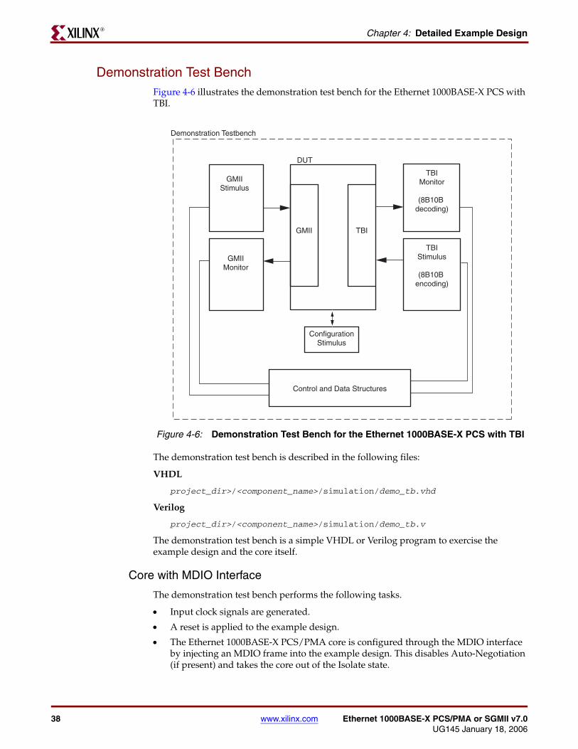
Demonstration Test BenchFigure 4-6 illustrates the demonstration test bench for the Ethernet 1000BASE-X PCS with TBI.
The demonstration test bench is described in the following files:
VHDL
project_dir>/<component_name>/simulation/demo_tb.vhd
Verilog
project_dir>/<component_name>/simulation/demo_tb.v
The demonstration test bench is a simple VHDL or Verilog program to exercise the example design and the core itself.
Core with MDIO Interface
The demonstration test bench performs the following tasks.
• Input clock signals are generated.
• A reset is applied to the example design.
• The Ethernet 1000BASE-X PCS/PMA core is configured through the MDIO interface by injecting an MDIO frame into the example design. This disables Auto-Negotiation (if present) and takes the core out of the Isolate state.
Figure 4-6: Demonstration Test Bench for the Ethernet 1000BASE-X PCS with TBI
TBIMonitor
(8B10B decoding)
TBIStimulus
(8B10B encoding)
GMIIStimulus
GMIIMonitor
GMII TBI
DUT
Demonstration Testbench
Control and Data Structures
ConfigurationStimulus

Ethernet 1000BASE-X PCS/PMA or SGMII v7.0 www.xilinx.com 39UG145 January 18, 2006
Core Example Design with Ten-Bit InterfaceR
• The following frames are injected into the GMII transmitter by the GMII stimulus block.
- the first is a minimum-length frame
- the second is a type frame
- the third is an errored frame
- the fourth is a padded frame
• The data received at the TBI transmitter interface is 8B10B decoded. The resultant frames are checked by the TBI Monitor against the stimulus frames injected into the GMII transmitter to ensure data integrity.
• The same four frames are generated by the TBI Stimulus block. These are 8B10B encoded and injected into the TBI receiver interface.
• Data frames received at the GMII receiver are checked by the GMII Monitor against the stimulus frames injected into the TBI receiver to ensure data integrity.
Core without MDIO Interface
The demonstration test bench performs the following tasks.
• Input clock signals are generated.
• A reset is applied to the example design.
• The Ethernet 1000BASE-X PCS/PMA core is configured via the Configuration Vector to take the core out of the Isolate state.
• The following frames are injected into the GMII transmitter by the GMII stimulus block.
- the first is a minimum length frame
- the second is a type frame
- the third is an errored frame
- the fourth is a padded frame
• The data received at the TBI transmitter interface is 8B10B decoded. The resultant frames are checked by the TBI Monitor against the stimulus frames injected into the GMII transmitter to ensure data is the same.
• The same four frames are generated by the TBI Stimulus block. These are 8B10B encoded and injected into the TBI receiver interface.
• Data frames received at the GMII receiver are checked by the GMII Monitor against the stimulus frames injected into the TBI receiver to ensure data is the same.
Customizing the Test BenchThis section provides information about making modifications to the demonstration test bench files.
Changing Frame Data
You can change the contents of the four frames used by the demonstration test bench by changing the data and valid fields for each frame defined in the test bench. Frames can be added by defining a new frame of data. Any modified frames are automatically updated in both stimulus and monitor functions.
40 www.xilinx.com Ethernet 1000BASE-X PCS/PMA or SGMII v7.0UG145 January 18, 2006
Chapter 4: Detailed Example DesignR
Changing Frame Error Status
Errors can be inserted into any of the predefined frames in any position by setting the “error” field to ‘1’ in any column of that frame. Injected errors are automatically updated in both stimulus and monitor functions.
Changing the Core Configuration
The configuration of the Ethernet 1000BASE-X PCS/PMA core used in the demonstration test bench can be altered.
Caution: Certain configurations of the core can cause the test bench to fail, or to cause processes to run indefinitely. For example, the demonstration test bench will not auto-negotiate with the design example. Determine the configurations that can safely be used with the test bench.
If the MDIO interface option has been selected, the core can be reconfigured by editing the injected MDIO frame in the demonstration test bench. See the Xilinx LogiCORE Ethernet 1000BASE-X PCS/PMA or SGMII User Guide for more information about using the MDIO interface.
If the MDIO interface option has not been selected, the core can be reconfigured by modifying the configuration vector directly. See the Xilinx LogiCORE Ethernet 1000BASE-X PCS/PMA or SGMII User Guide for information about using the configuration vector.
SGMII Example Design / Dynamic Switching Example DesignNote: This is the example design provided when the core is generated for the SGMII standard; it is also provided when the core is generated with the 1000BASE-X/SGMII dynamic switching capability.
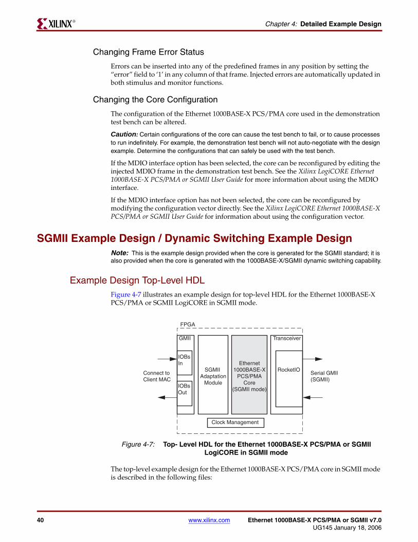
Example Design Top-Level HDLFigure 4-7 illustrates an example design for top-level HDL for the Ethernet 1000BASE-X PCS/PMA or SGMII LogiCORE in SGMII mode.
The top-level example design for the Ethernet 1000BASE-X PCS/PMA core in SGMII mode is described in the following files:
Figure 4-7: Top- Level HDL for the Ethernet 1000BASE-X PCS/PMA or SGMII LogiCORE in SGMII mode
Ethernet1000BASE-X
PCS/PMACore
(SGMII mode)
FPGA
RocketIO
TransceiverGMII
IOBsIn
IOBsOut
SGMII Adaptation
Module
Clock Management
Connect toClient MAC
Serial GMII(SGMII)

Ethernet 1000BASE-X PCS/PMA or SGMII v7.0 www.xilinx.com 41UG145 January 18, 2006
SGMII Example Design / Dynamic Switching Example DesignR
VHDL
project_dir>/<component_name>/example_design/<component_name>_top.vhd
Verilog
project_dir>/<component_name>/example_design/<component_name>_top.v
The example design HDL top level contains the following:
• An instance of the Ethernet 1000BASE-X PCS/PMA core in SGMII mode.
• An instance of a Virtex-II Pro or Virtex-4 RocketIO transceiver.
• Clock management logic for the core and the RocketIO transceiver, including DCM and Global Clock Buffer instances.
• An SGMII adaptation module containing:
- The clock management logic required to enable the SGMII example design to operate at 10 Mbps, 100 Mbps, and 1 Gbps
- GMII logic for both transmitter and receiver paths; the GMII style 8-bit interface is run at 125 MHz for 1 Gbps operation; 12.5 MHz for 100 Mbps operation; 1.25 MHz for 10 Mbps operation.
• External GMII logic, including IOB and DDR register instances, where required.
• Input and output buffers for other port signals of the example design top level.
The example design HDL top-level connects the GMII of the core to the SGMII adaptation module and the PHY side interface of the core directly to a RocketIO instance. This allows the functionality of the core to be demonstrated using a simulation package, as described in this guide.
TransceiverA wrapper file for the Virtex-II Pro RocketIO or Virtex-4 Multi-Gigabit Transceiver is described in the following files:
VHDL
project_dir>/<component_name>/example_design/transceiver.vhd
Verilog
project_dir>/<component_name>/example_design/transceiver.v
This file instances a Virtex-II Pro RocketIO or Virtex-4 RocketIO and applies Gigabit Ethernet 1000BASE-X attributes to it. This transceiver wrapper is instantiated from the top-level HDL file for the example design.
For Virtex-4 FX devices only, a Calibration Block is required. See the Calibration Block Users Guide for more information.
This is decribed in the following files: VHDL
project_dir/<component_name>/example_design/cal_block_v1_2_1.vhd
Verilog
project_dir/<component_name>/example_design/cal_block_v1_2_1.v
42 www.xilinx.com Ethernet 1000BASE-X PCS/PMA or SGMII v7.0UG145 January 18, 2006
Chapter 4: Detailed Example DesignR
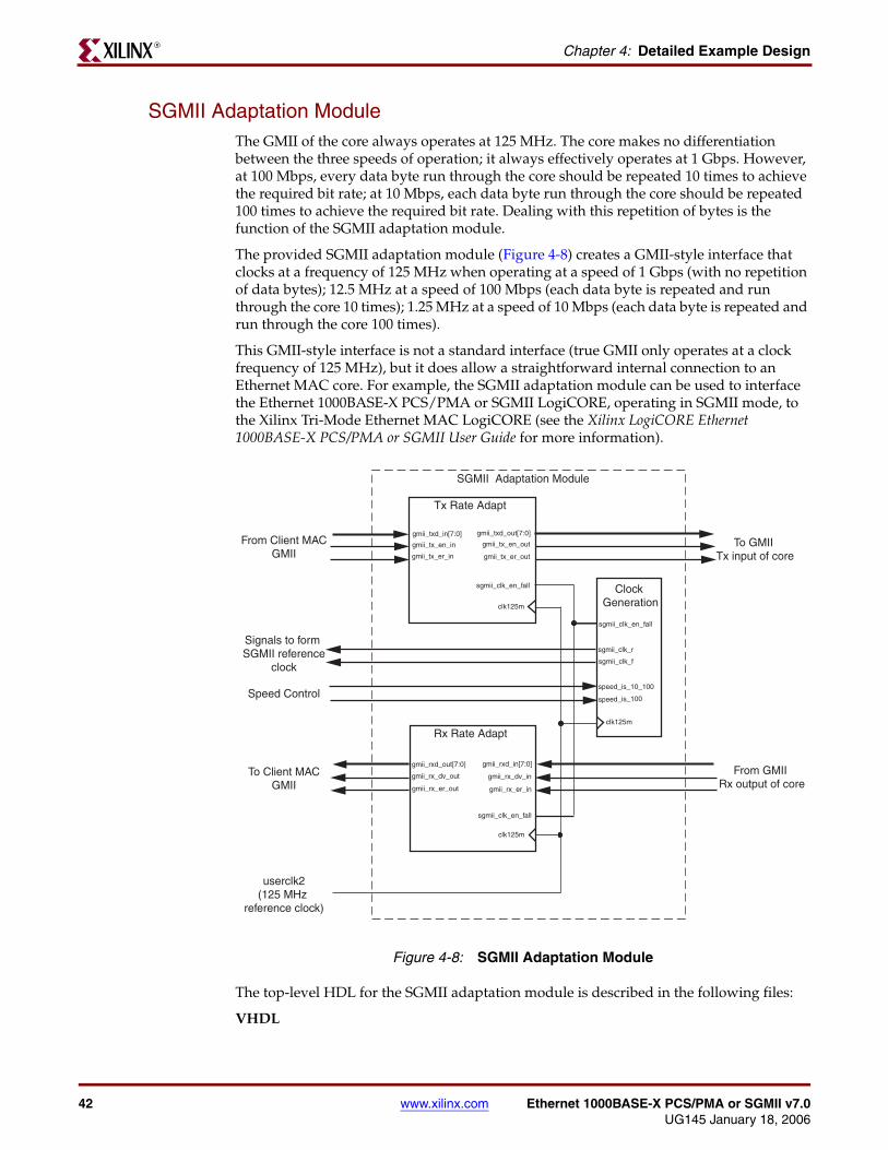
SGMII Adaptation ModuleThe GMII of the core always operates at 125 MHz. The core makes no differentiation between the three speeds of operation; it always effectively operates at 1 Gbps. However, at 100 Mbps, every data byte run through the core should be repeated 10 times to achieve the required bit rate; at 10 Mbps, each data byte run through the core should be repeated 100 times to achieve the required bit rate. Dealing with this repetition of bytes is the function of the SGMII adaptation module.
The provided SGMII adaptation module (Figure 4-8) creates a GMII-style interface that clocks at a frequency of 125 MHz when operating at a speed of 1 Gbps (with no repetition of data bytes); 12.5 MHz at a speed of 100 Mbps (each data byte is repeated and run through the core 10 times); 1.25 MHz at a speed of 10 Mbps (each data byte is repeated and run through the core 100 times).
This GMII-style interface is not a standard interface (true GMII only operates at a clock frequency of 125 MHz), but it does allow a straightforward internal connection to an Ethernet MAC core. For example, the SGMII adaptation module can be used to interface the Ethernet 1000BASE-X PCS/PMA or SGMII LogiCORE, operating in SGMII mode, to the Xilinx Tri-Mode Ethernet MAC LogiCORE (see the Xilinx LogiCORE Ethernet 1000BASE-X PCS/PMA or SGMII User Guide for more information).
The top-level HDL for the SGMII adaptation module is described in the following files:
VHDL
Figure 4-8: SGMII Adaptation Module
SGMII Adaptation Module
Tx Rate Adapt
Clock Generation
To GMII Tx input of core
From GMII Rx output of core
From Client MACGMII
To Client MACGMII
Signals to form SGMII reference
clock
userclk2(125 MHz
reference clock)
sgmii_clk_en_fall
sgmii_clk_r
clk125m
speed_is_10_100
speed_is_100
sgmii_clk_f
clk125m
sgmii_clk_en_fall
gmii_txd_in[7:0] gmii_txd_out[7:0]
gmii_tx_en_in gmii_tx_en_out
gmii_tx_er_in gmii_tx_er_out
Rx Rate Adapt
clk125m
sgmii_clk_en_fall
gmii_rxd_out[7:0] gmii_rxd_in[7:0]
gmii_rx_dv_out gmii_rx_dv_in
gmii_rx_er_out gmii_rx_er_in
Speed Control
Ethernet 1000BASE-X PCS/PMA or SGMII v7.0 www.xilinx.com 43UG145 January 18, 2006
SGMII Example Design / Dynamic Switching Example DesignR
project_dir>/<component_name>/example_design/sgmii_adapt/
sgmii_adapt.vhd
Verilog
project_dir>/<component_name>/example_design/sgmii_adapt/
sgmii_adapt.v
The SGMII adaptation module is described in several hierarchical sub-modules as illustrated in Figure 4-8. These sub-modules are described in separate HDL files as shown below.
Note that the 125 MHz reference clock (clk125m) used by the SGMII Adaptation logic is userclk2. This is the 125 MHz clock used to clock the Ethernet 1000BASE-X PCS/PMA or SGMII core and the clock routed to TXUSRCLK2 and RXUSRCLK2 of the RocketIO.
Clock GenerationThe clock generation module is described in the following files:
VHDL
project_dir>/<component_name>/example_design/sgmii_adapt/clk_gen.vhd
Verilog
project_dir>/<component_name>/example_design/sgmii_adapt/clk_gen.v
This file creates the necessary clocks and clock enables for use throughout the SGMII adaptation module. Clock frequencies are:
• 125 MHz at an operating speed of 1 Gbps
• 12.5 MHz at an operating speed of 100 Mbps
• 1.25 MHz at an operating speed of 10 Mbps
Figure 4-9 illustrates the output clock and clock enable signals for the Clock Generation module at 1 Gbps and 100 Mbps speeds.
At 1 Gbps, sgmii_clk_r is fixed at logic 0; sgmii_clk_f is fixed at logic 1. sgmii_clk_r is connected to the rising edge triggered flip-flop of an IOB output DDR, clocked with clk125m. sgmii_clk_f is connected to the falling edge triggered flip-flop of the same IOB output DDR. The result is the production of an inverted clock, sgmii_clk, that is forwarded off-chip. This IOB DDR output register is included in the top level HDL for the example design.
At 100 Mbps, the sgmii_clk_r and sgmii_clk_f signals toggle at the required clock frequency (every five clock periods of clk125m), also illustrated in Figure 4-9. sgmii_clk_r is synchronous to the rising edge of the 125 MHz reference clock (clk125m); sgmii_clk_f is synchronous to the falling edge of the clk125m. These are routed to the rising and falling edges of the IOB DDR output register to forward the SGMII reference clock (sgmii_clk) off chip.
At 10 Mbps, the situation is identical to that of 100 Mbps, with the exception that sgmii_clk_r and sgmii_clk_f toggle every 50 clock periods of clk125m.
sgmii_clk_en_fall is used as a clock enable throughout the SGMII adaptation logic. At 1 Gbps it is fixed at logic 1 indicating that every clk125m period is significant. At 100 Mbps, this signal is valid for a single period of clk125m every ten clocks and marks the falling edge of the SGMII reference clock, sgmii_clk. At 10 Mbps, this signal is valid for a single period of clk125m every one hundred clocks and again marks the falling edge
44 www.xilinx.com Ethernet 1000BASE-X PCS/PMA or SGMII v7.0UG145 January 18, 2006
Chapter 4: Detailed Example DesignR
sgmii_clk. This clock enable signal is used as the control for the data byte repetition in the Transmitter and Receiver Rate Adaptation modules.

Ethernet 1000BASE-X PCS/PMA or SGMII v7.0 www.xilinx.com 45UG145 January 18, 2006
SGMII Example Design / Dynamic Switching Example DesignR
Figure 4-9 shows the clock generator output clocks and clock enable configurations.
Johnson CounterThe Johnson Counter is described in the following files:
VHDL
project_dir>/<component_name>/example_design/sgmii_adapt/
johnson_cntr.vhd
Verilog
project_dir>/<component_name>/example_design/sgmii_adapt/
johnson_cntr.v
Figure 4-9: Clock Generator Output Clocks and Clock Enable
sgmii_clk_r
clk125 m
sgmii_clk_f
sgmii_clk_en_fall
sgmii_clk_r
sgmii_clk_f
sgmii_clk_en_fall
5 clk125 m cycles
'0'
'1'
'1'
Speed is 1 Gbps
Speed is 100 Mbps
clk125 m
10 clk125 m cycles
sgmii_clk(result of IOBoutput DDR)
sgmii_clk(result of IOBoutput DDR)

46 www.xilinx.com Ethernet 1000BASE-X PCS/PMA or SGMII v7.0UG145 January 18, 2006
Chapter 4: Detailed Example DesignR
The Johnson Counter is instantiated twice by the clock generation circuitry. The Johnson Counter is a shift register based clock divider that provides a divide-by-ten clock output.
The divide-by-ten clock is output directly from a flip-flop triggered on the rising edge of the 125 MHz reference clock, clk125m.
Johnson Counter capabilities are extended by using the clock enables; it is only the clock-enabled cycles that trigger the shift register, and are therefore divided down.
Transmitter Rate Adaptation ModuleThe Transmitter Rate Adaptation module is described in the following files:
VHDL
project_dir>/<component_name>/example_design/sgmii_adapt/
tx_rate_adapt.vhd
Verilog
project_dir>/<component_name>/example_design/sgmii_adapt/
tx_rate_adapt.v
This module accepts transmitter data from the GMII-style interface from the attached client MAC, and samples the input data on the 125 MHz reference clock, clk125m. This sampled data can then be connected directly to the input GMII of the Ethernet 1000BASE-X PCS/PMA or SGMII core. The 1 Gbps and 100 Mbps cases are illustrated in Figure 4-10.
At 1 Gbps the client MAC should drive the GMII transmitter data synchronously to the rising edge of clk125m. sgmii_clk_en_fall (derived from the Clock Generation module) is fixed at logic 1 and the input data is sampled on every clock cycle.
At 100 Mbps and 10 Mbps, the client MAC should drive the GMII transmitter data synchronously to the rising edge of sgmii_clk. The data is sampled (see Figure 4-10) on the sgmii_clk_en_fall pulse. Since this pulse marks the falling edge of sgmii_clk, it guarantees that the data is stable when sampled. The frequency of the sgmii_clk_en_fall pulse ensures that this data is repeated exactly 10 times when operating at a speed of 100 Mbps and 100 times when operating at a speed of 10 Mbps.

Ethernet 1000BASE-X PCS/PMA or SGMII v7.0 www.xilinx.com 47UG145 January 18, 2006
SGMII Example Design / Dynamic Switching Example DesignR
Receiver Rate Adaptation ModuleThe Receiver Rate Adaptation module is described in the following files:
VHDL
project_dir>/<component_name>/example_design/sgmii_adapt/
rx_rate_adapt.vhd
Verilog
project_dir>/<component_name>/example_design/sgmii_adapt/
rx_rate_adapt.v
This module accepts received data from the Ethernet 1000BASE-X PCS/PMA or SGMII core. This data is sampled and sent out of the GMII receiver interface for the attached client MAC. The 1 Gbps and 100 Mbps cases are illustrated in Figure 4-11.
At 1 Gbps, the data is valid on every clock cycle of the 125 MHz reference clock (clk125m). Data received from the core is clocked straight through the Receiver Rate Adaptation module.
Figure 4-10: Transmitter Rate Adaptation Module Data Sampling
sgmii_clk_en_fall
clk125 m
'1'
Speed is 1 Gbps
D0 D1 D2
D0 D1 D2
gmii_txd_in[7:0]
gmii_txd_out[7:0]
sgmii_clk_en_fall
Speed is 100 Mbps
gmii_txd_in[7:0]
gmii_txd_out[7:0]
D0
D0
D1
D1
D2
10 clk125 m cycles
clk125 m
sgmii_clk
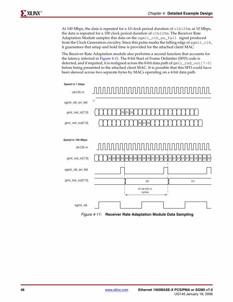
48 www.xilinx.com Ethernet 1000BASE-X PCS/PMA or SGMII v7.0UG145 January 18, 2006
Chapter 4: Detailed Example DesignR
At 100 Mbps, the data is repeated for a 10 clock period duration of clk125m; at 10 Mbps, the data is repeated for a 100 clock period duration of clk125m. The Receiver Rate Adaptation Module samples this data on the sgmii_clk_en_fall signal produced from the Clock Generation circuitry. Since this pulse marks the falling edge of sgmii_clk, it guarantees that setup and hold time is provided for the attached client MAC.
The Receiver Rate Adaptation module also performs a second function that accounts for the latency inferred in Figure 4-11. The 8-bit Start of Frame Delimiter (SFD) code is detected, and if required, it is realigned across the 8-bit data path of gmii_rxd_out[7:0] before being presented to the attached client MAC. It is possible that this SFD could have been skewed across two separate bytes by MACs operating on a 4-bit data path.
Figure 4-11: Receiver Rate Adaptation Module Data Sampling
sgmii_clk_en_fall
clk125 m
'1'
Speed is 1 Gbps
D0 D1 D2
D0 D1 D2
gmii_rxd_in[7:0]
gmii_rxd_out[7:0]
sgmii_clk_en_fall
Speed is 100 Mbps
gmii_rxd_in[7:0]
gmii_txd_out[7:0] D0 D1
10 clk125 m cycles
clk125 m
sgmii_clk
D0 D1 D2D0 D0 D0D0D0D0 D0 D0 D0 D1 D1 D1 D1 D1 D1 D1 D1 D1 D2 D2 D2
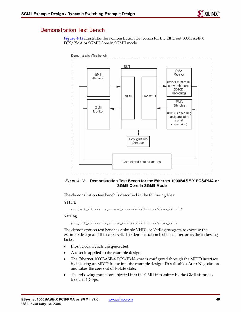
Ethernet 1000BASE-X PCS/PMA or SGMII v7.0 www.xilinx.com 49UG145 January 18, 2006
SGMII Example Design / Dynamic Switching Example DesignR
Demonstration Test BenchFigure 4-12 illustrates the demonstration test bench for the Ethernet 1000BASE-X PCS/PMA or SGMII Core in SGMII mode.
The demonstration test bench is described in the following files:
VHDL
project_dir>/<component_name>/simulation/demo_tb.vhd
Verilog
project_dir>/<component_name>/simulation/demo_tb.v
The demonstration test bench is a simple VHDL or Verilog program to exercise the example design and the core itself. The demonstration test bench performs the following tasks.
• Input clock signals are generated.
• A reset is applied to the example design.
• The Ethernet 1000BASE-X PCS/PMA core is configured through the MDIO interface by injecting an MDIO frame into the example design. This disables Auto-Negotiation and takes the core out of Isolate state.
• The following frames are injected into the GMII transmitter by the GMII stimulus block at 1 Gbps.
Figure 4-12: Demonstration Test Bench for the Ethernet 1000BASE-X PCS/PMA or SGMII Core in SGMII Mode
PMAMonitor
(serial to parallelconversion and
8B10B decoding)
PMAStimulus
(8B10B encodingand parallel to
serial conversion)
GMIIStimulus
GMIIMonitor
GMII RocketIO
DUT
Demonstration Testbench
Control and data structures
ConfigurationStimulus

50 www.xilinx.com Ethernet 1000BASE-X PCS/PMA or SGMII v7.0UG145 January 18, 2006
Chapter 4: Detailed Example DesignR
- the first is a minimum length frame
- the second is a type frame
- the third is an errored frame
- the fourth is a padded frame
• The serial data received at the RocketIO transmitter interface is converted to 10-bit parallel data, then 8B10B decoded. The resultant frames are checked by the PMA Monitor against the stimulus frames injected into the GMII transmitter to ensure data integrity.
• The same four frames are generated by the PMA Stimulus block. These are 8B10B encoded, converted to serial data and injected into the RocketIO receiver interface at 1 Gbps.
• Data frames received at the GMII receiver are checked by the GMII Monitor against the stimulus frames injected into the RocketIO receiver to ensure data integrity.
Customizing the Test Bench
Changing Frame Data
You can change the contents of the four frames used by the demonstration test bench by changing the data and valid fields for each frame defined in the test bench. New frames can be added by defining a new frame of data. Modified frames are automatically updated in both stimulus and monitor functions.
Changing Frame Error Status
Errors can be inserted into any of the predefined frames in any position by setting the “error” field to ‘1’ in any column of that frame. Injected errors are automatically updated in both stimulus and monitor functions.
Changing the Core Configuration
The configuration of the Ethernet 1000BASE-X PCS/PMA core used in the demonstration test bench can be altered.
Caution: Certain configurations of the core cause the test bench to fail, or to cause processes to run indefinitely. For example, the demonstration test bench will not Auto-Negotiate with the design example. Determine the configurations that can safely be used with the test bench.
The core can be reconfigured by editing the injected MDIO frame in the demonstration test bench. See the Xilinx LogiCORE Ethernet 1000BASE-X PCS/PMA or SGMII User Guide for information about using the MDIO interface.
Changing the Operational Speed
SGMII can be used to carry ethernet traffic at 10 Mbps, 100 Mbps or 1 Gbps. By default, the demonstration test bench is configured to operate at 1 Gbps. The speed of both the example design and test bench can be set to the desired operational speed by editing the following settings, recompiling the test bench, then running the simulation again.
1 Gbps operation
set speed_is_10_100 to logic 0
Ethernet 1000BASE-X PCS/PMA or SGMII v7.0 www.xilinx.com 51UG145 January 18, 2006
SGMII Example Design / Dynamic Switching Example DesignR
100 Mbps operation
set speed_is_10_100 to logic 1
set speed_is_100 to logic 1
10 Mbps operation
set speed_is_10_100 to logic 1
set speed_is_100 to logic 0

52 www.xilinx.com Ethernet 1000BASE-X PCS/PMA or SGMII v7.0UG145 January 18, 2006
Chapter 4: Detailed Example DesignR