lmg1210 200-v, 1.5-a, 3-a half-bridge gan driver with ... · 5-apr-2018 addendum-page 1 packaging...
TRANSCRIPT
AD
VA
NC
E I
NF
OR
MA
TIO
N
LDO
UVLOOTP
Delay Match
HB
BST
VIN
EN
PWM
DHL DLH
6 ± 18 V
200 V
HO
HS
5 VVDD
LO
VSS
EN
PWMDead Time
Copyright © 2018, Texas Instruments Incorporated
Product
Folder
Order
Now
Technical
Documents
Tools &
Software
Support &Community
An IMPORTANT NOTICE at the end of this data sheet addresses availability, warranty, changes, use in safety-critical applications,intellectual property matters and other important disclaimers. ADVANCE INFORMATION for pre-production products; subject tochange without notice.
LMG1210SNOSD12A –FEBRUARY 2018–REVISED MAY 2018
LMG1210 200-V, 1.5-A, 3-A Half-Bridge GaN Driver With Adjustable Dead Time
1
1 Features1• Ultra-High Speed Operation of 50 MHz
– 10 ns Typical Propagation Delay– 1.5 ns High-Side to Low-Side Matching– Pulse Width ≥ 3 ns
• 1.5-A Peak Source and 3.1-A Peak Sink Currents• Adjustable Dead-Time Control Feature• Highest Slew Rate Immunity in Industry of 300
V/ns• External Bootstrap Diode For Flexibility• High-Side to Low-Side Capacitance Less Than 1
pF• UVLO and Overtemperature Protection• Low-Inductance WQFN Package
2 Applications• High-Speed DC-DC Converters• RF Envelope Tracking• Class-D Audio Amplifiers• Class-E Wireless Charging
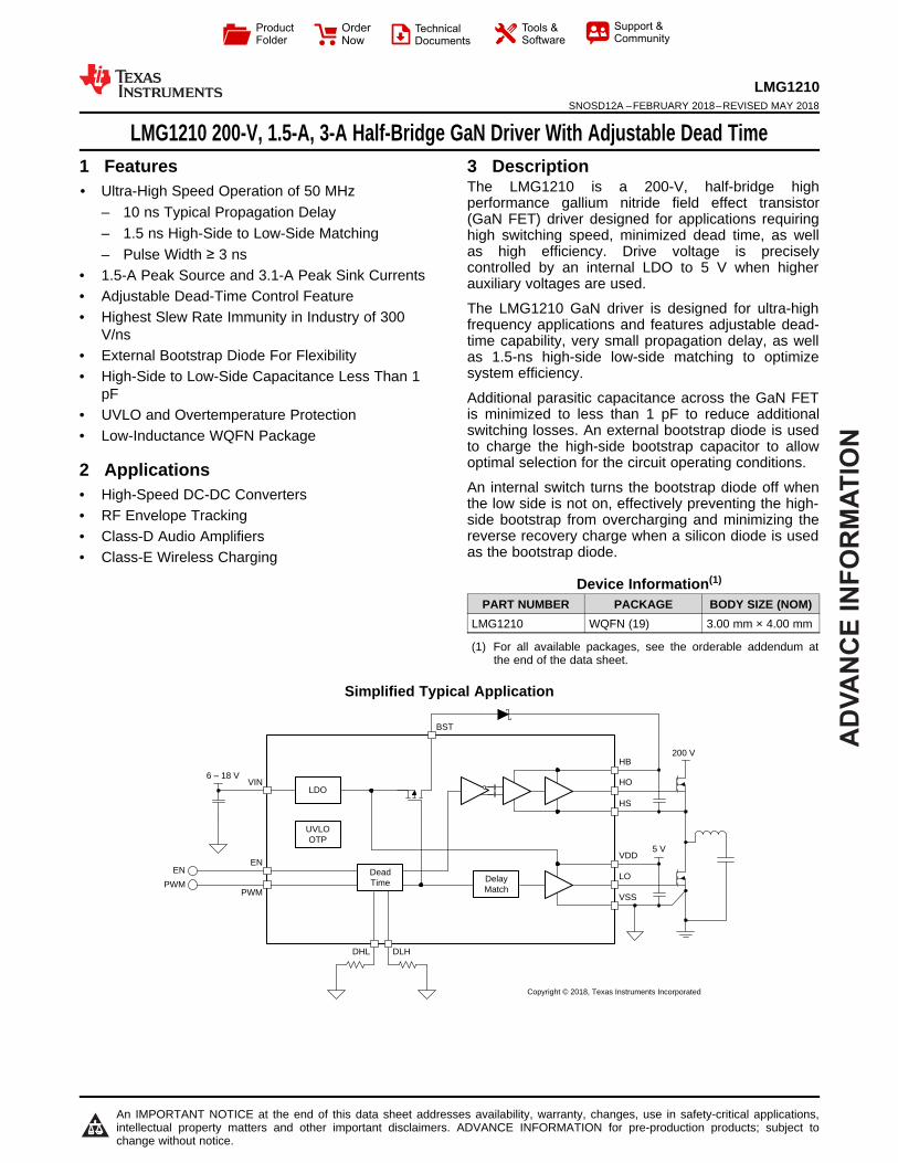
3 DescriptionThe LMG1210 is a 200-V, half-bridge highperformance gallium nitride field effect transistor(GaN FET) driver designed for applications requiringhigh switching speed, minimized dead time, as wellas high efficiency. Drive voltage is preciselycontrolled by an internal LDO to 5 V when higherauxiliary voltages are used.
The LMG1210 GaN driver is designed for ultra-highfrequency applications and features adjustable dead-time capability, very small propagation delay, as wellas 1.5-ns high-side low-side matching to optimizesystem efficiency.
Additional parasitic capacitance across the GaN FETis minimized to less than 1 pF to reduce additionalswitching losses. An external bootstrap diode is usedto charge the high-side bootstrap capacitor to allowoptimal selection for the circuit operating conditions.
An internal switch turns the bootstrap diode off whenthe low side is not on, effectively preventing the high-side bootstrap from overcharging and minimizing thereverse recovery charge when a silicon diode is usedas the bootstrap diode.
Device Information(1)
PART NUMBER PACKAGE BODY SIZE (NOM)LMG1210 WQFN (19) 3.00 mm × 4.00 mm
(1) For all available packages, see the orderable addendum atthe end of the data sheet.
Simplified Typical Application

AD
VA
NC
E IN
FO
RM
AT
ION
2
LMG1210SNOSD12A –FEBRUARY 2018–REVISED MAY 2018 www.ti.com
Product Folder Links: LMG1210
Submit Documentation Feedback Copyright © 2018, Texas Instruments Incorporated
Table of Contents1 Features .................................................................. 12 Applications ........................................................... 13 Description ............................................................. 14 Revision History..................................................... 25 Description (continued)......................................... 26 Pin Configuration and Functions ......................... 37 Specifications......................................................... 4
7.1 Absolute Maximum Ratings ...................................... 47.2 ESD Ratings ............................................................ 47.3 Recommended Operating Conditions....................... 47.4 Thermal Information ................................................. 57.5 Electrical Characteristics........................................... 57.6 Switching Characteristics .......................................... 7
8 Detailed Description .............................................. 88.1 Overview ................................................................... 88.2 Functional Block Diagram ......................................... 88.3 Feature Description................................................... 8
8.4 Device Functional Modes........................................ 109 Application and Implementation ........................ 11
9.1 Application Information............................................ 119.2 Typical Application ................................................. 119.3 Do's and Don'ts ...................................................... 14
10 Power Supply Recommendations ..................... 1511 Layout................................................................... 15
11.1 Layout Guidelines ................................................. 1511.2 Layout Example .................................................... 16
12 Device and Documentation Support ................. 1712.1 Documentation Support ....................................... 1712.2 Receiving Notification of Documentation Updates 1712.3 Community Resources.......................................... 1712.4 Trademarks ........................................................... 1712.5 Electrostatic Discharge Caution............................ 1712.6 Glossary ................................................................ 17
13 Mechanical, Packaging, and OrderableInformation ........................................................... 17
4 Revision History
Changes from Original (February 2018) to Revision A Page
• Changed Thermal Pad Pins and NC in Pin Functions table ................................................................................................. 3• Changed Power Supply Recommendations text. ................................................................................................................ 15• Changed layout example. ..................................................................................................................................................... 16
5 Description (continued)The GaN driver can operate in two different modes: independent input mode (IIM) and PWM mode. In the IIMeach of the outputs is independently controller by a dedicated input. In PWM mode the two complementaryoutput signals are generated from a single input, and the user can adjust the dead time from 0 to 20 ns for eachedge. The LMG1210 operates over a wide temperature range from –40°C to 125°C and is offered in a low-inductance WQFN package.

AD
VA
NC
E I
NF
OR
MA
TIO
N
PWM/LI
EN/HI
BST
Thermal Pad
HB
NC
1
HS
NC
NC
HO
HS
GND
LO
NC
GN
D
VD
D
VIN
DH
L
DLH
HS
1 2 3 4 5
15 14 13 12 11
10
9
8
7
6
16
17
18
19
(HS)
(GND)
3
LMG1210www.ti.com SNOSD12A –FEBRUARY 2018–REVISED MAY 2018
Product Folder Links: LMG1210
Submit Documentation FeedbackCopyright © 2018, Texas Instruments Incorporated
6 Pin Configuration and Functions
RVR Package19-Pin WQFN
Top View
Pin FunctionsPIN I/O DESCRIPTION
NC 1,11,15 n/a Not internally connected.VIN 2 I 6 V to 18 V input to LDO. If LDO is not required, connect to VDD.GND 3,7 I Low-side ground return: all low-side signals are referenced to this ground.VDD 4 O Low-side driver supply and LDO output. 5 VDHL 5 I Sets the dead time for a high-to-low transition in PWM mode by connecting a resistor to GND.DLH 6 I Sets the dead time for a low-to-high transition in PWM mode by connecting a resistor to GND.
Tie to VDD to select independent input mode.LO 8 O Low-side driver output.HS 9,13,16 I Switched node and high-side driver ground. These pins are internally connected; external
connection on board is recommended.HO 10 O High-side driver output.HB 12 I High-side driver supply.BST 17 O Bootstrap diode anode connection point.EN/HI 18 I Enable input or high-side driver control.PWM/LI 19 I PWM input or low-side driver control.Thermal Pad(HS) 21 I Connected to HS, must be connected.
Thermal Pad(GND) 20 I Connected to GND, must be connected.
NC1 14 NC For proper operation, this pin should be either unconnected or tied to HS.

AD
VA
NC
E IN
FO
RM
AT
ION
4
LMG1210SNOSD12A –FEBRUARY 2018–REVISED MAY 2018 www.ti.com
Product Folder Links: LMG1210
Submit Documentation Feedback Copyright © 2018, Texas Instruments Incorporated
(1) Stresses beyond those listed under Absolute Maximum Ratings may cause permanent damage to the device. These are stress ratingsonly, which do not imply functional operation of the device at these or any other conditions beyond those indicated under RecommendedOperating Conditions. Exposure to absolute-maximum-rated conditions for extended periods may affect device reliability.
7 Specifications
WARNINGAPPLICABLE TO PRE-PRODUCTION UNITS:Pre-production units have a silicon issue which causes the low-side bootstrapswitch to enter into a high-current state if a short L-H-L pulse is applied to thelow-side driver. The exciting pulse width is typically about 3 ns. The high-current state consumes an extra 140 mA typical. from the VDD rail. The part willrecover when a wider pulse is applied. This issue will be fixed for productionunits.
7.1 Absolute Maximum RatingsOver operating free-air temperature range (unless otherwise noted) (1)
MIN MAX UNITVIN Input Supply Voltage -0.5 20 VVDD 5V Supply Voltage -0.5 5.5 VVHS High Side Voltage Without Bootstrap Diode -300 300 VVHB-VHS Bootstrap supply voltage, continuous -0.5 5.5 VVLI/PWM, VHI/EN Input Pin Voltage on LI or HI -0.5 10 VVDHL, VDHL Voltage on DLH and DHL pins -0.5 VDD + 0.5VLO Low-side gate driver output -0.5 VDD + 0.5VHO High-side gate driver output VHS-0.5 VHB+ 0.5VBST Bootstrap pin voltage -0.5 VDD + 0.5TJ Operating Temperature -40 150 °C
(1) JEDEC document JEP155 states that 500-V HBM allows safe manufacturing with a standard ESD control process. Manufacturing withless than 500-V HBM is possible with the necessary precautions. Pins listed as ±XXX V may actually have higher performance.
(2) JEDEC document JEP157 states that 250-V CDM allows safe manufacturing with a standard ESD control process. Manufacturing withless than 250-V CDM is possible with the necessary precautions. Pins listed as ±YYY V may actually have higher performance.
7.2 ESD RatingsVALUE UNIT
V(ESD) Electrostatic dischargeHuman-body model (HBM), per ANSI/ESDA/JEDEC JS-001 (1) ±2000
VCharged-device model (CDM), per JEDEC specification JESD22-C101 (2) ±500
7.3 Recommended Operating Conditionsover operating free-air temperature range (unless otherwise noted)
MIN NOM MAX UNITVIN Input Supply Voltage (if using internal LDO) 6 18 VVDD 5V Supply Voltage 4.75 5.00 5.25 VVHS-VSS High-Side Voltage with Bootstrap Diode -VDD-0.5 200 VVHS-VSS High-Side Voltage Without Bootstrap diode -200 200 VVHB-VHS Bootstrap Supply Voltage 3.70 5.25 VVLIHI Input Pin Voltage -0.3 10 VTJ Operating Temperature -40 125 °CCMTI High Side Slew Rate 300 V/ns

AD
VA
NC
E I
NF
OR
MA
TIO
N
5
LMG1210www.ti.com SNOSD12A –FEBRUARY 2018–REVISED MAY 2018
Product Folder Links: LMG1210
Submit Documentation FeedbackCopyright © 2018, Texas Instruments Incorporated
(1) For more information about traditional and new thermal metrics, see the Semiconductor and IC Package Thermal Metrics applicationreport.
7.4 Thermal Information
THERMAL METRIC (1)LMG1210
UNITRVR (QFN)19 PINS
RθJA Junction-to-ambient thermal resistance 40.5 °C/WRθJC(top) Junction-to-case (top) thermal resistance 40 °C/WRθJB Junction-to-board thermal resistance 16.2 °C/WψJT Junction-to-top characterization parameter 2.9 °C/WψJB Junction-to-board characterization parameter 16.4 °C/W
(1) Ensured by design
7.5 Electrical CharacteristicsPARAMETER TEST CONDITIONS MIN TYP MAX UNIT
SUPPLY CURRENT
IDD5V Quiescent Current, Low-SideCircuits Only
LI,HI=0V, Independent Mode 250 400 μAEN=0V, PWM=X, PWM Input Mode,DHL and DLH floating 325 500 μA
IHB HB Quiescent Current HI=0V , Independent Mode 520 800 μAIHBS HB to VSS Quiescent Current VHS=100V 25 nAIHBSO HB to VSS Operating Current VHS=100V, FSW=1MHz 1 nAILSDyn Low-side dynamic current Unloaded, PWM Mode 1 1.25 mA/MHzIHSDyn High-side dynamic current Unloaded 0.5 0.6 mA/MHzLOW-SIDE TO HIGH-SIDE CAPACITANCE
CISO Capacitance from High to Low Side Low Side Pins Shorted Together,High Side Pins Shorted Together 0.25 pF
5V LDOV5V LDO Output 4.75 5.00 5.25 VVDO Dropout Voltage IO=100mA 400 750 mVILDOM Maximum Current 100 mAISC Short Circuit Current 110 250 mA
COUTMinimal Required OutputCapacitance (1) Effective Capacitance at Bias 0.3 µF
CESR Bypass Capacitor ESR (1) 0 500 mΩDIGITAL INPUT PINS (LI/PWM & HI/EN)VIR Input Rising Edge Threshold 1.70 2.45 VVIF Input Falling Edge Threshold 0.70 1.30 VVIHYS Input Hysteresis 1 VRIPD Input Pull-Down Resistance VLI,VHI=1V 100 200 300 kΩUNDERVOLTAGE LOCKOUTVDDR VDD Rising Threshold 4.00 4.25 4.50 VVDDH VDD Hysteresis 200 mVVHBR HB-HS Rising Threshold 3.40 3.55 3.70 VVHBH HB-HS Hysteresis 100 mVBOOTSTRAP DIODE SWITCHRSW Diode Switch On Resistance ID=100mA 0.4 0.5 ΩGATE DRIVERVOL Low-Level Output Voltage IOL=100mA 0.16 VVDD-VOH High-Level Output Voltage IOH=100mA 0.30 VIOL Peak Sink Current VOx=5V 2.2 3.1 4.3 A

AD
VA
NC
E IN
FO
RM
AT
ION
6
LMG1210SNOSD12A –FEBRUARY 2018–REVISED MAY 2018 www.ti.com
Product Folder Links: LMG1210
Submit Documentation Feedback Copyright © 2018, Texas Instruments Incorporated
Electrical Characteristics (continued)PARAMETER TEST CONDITIONS MIN TYP MAX UNIT
IOH Peak Source Current VOx=0V 0.85 1.58 2.2 A
VCLAMP Unpowered Gate Clamp Voltage VDD,VHB Floating, 1 mA pull-upapplied to LO/HO 0.55 0.8 V
THERMAL SHUTDOWN
TSDThermal Shutdown Switching, RisingEdge (1) 150 180 °C
TSD_LDOThermal Shut Down LDO, RisingEdge (1) 160 190 °C
THYS_SDThermal Hysteresis, LDO &Switching (1) 3 10 °C
TSD_HS Thermal Shutdown for High-Side,Rising Edge (1)
160 190 °C
DEADTIME CONTROL RESISTORSRPU Internal Pullup Resistor 23.5 25 26.5 kΩVDT Dead Time Voltage Range 0.8 1.8 V
FCDEADDead Time Low Pass Filter CornerFrequency 10 kHz

AD
VA
NC
E I
NF
OR
MA
TIO
N
7
LMG1210www.ti.com SNOSD12A –FEBRUARY 2018–REVISED MAY 2018
Product Folder Links: LMG1210
Submit Documentation FeedbackCopyright © 2018, Texas Instruments Incorporated
(1) Mismatch defined as the maximum of |TpLH-TpHL| and |TpHL-TpLH|(2) Pulses longer than tPW, but shorter than tPW,ext get extended to tPW,ext
7.6 Switching CharacteristicsVDD=5V, VHB-HS=4.5V, over operating free-air temperature range (unless otherwise noted)
PARAMETER TEST CONDITIONS MIN TYP MAX UNITINDEPENDENT INPUT MODEtPHL Turn-Off Delay 10 18 nstPLH Turn-On Delay 10 18 ns
tMTCHHigh-Off to Low-On and Low-Off toHigh-On Delay Matching(1) Over temperature, TjHI=TjLO 0.3 1.2 ns
tMTCHHigh-Off to Low-On and Low-Off toHigh-On Delay Matching (1)
Signal propagating during a 150V/ns CMT event 1 ns
tMTCHHigh-Off to Low-On and Low-Off toHigh-On Delay Matching (1) TjHI=TjLO=25C 0.2 ns
PWM INPUT MODEtPHL Turn-Off Delay 11 21 nstPLH Turn-On Delay, tDEAD=0 11 21 nstDEAD_MIN Minimum Dead Time Open Rext -0.5 0 0.7 nstDEAD_MAX Maximum Dead Time 20k Rext 18 20 22 nstEN Enable Propagation Time 11 20 nsOTHER CHARACTERISTICStOR Output Rise Time, Unloaded 10%-90% 0.5 nstOF Output Fall Time, Unloaded 90%-10% 0.5 nstORL Output Rise Time, Loaded CO=1nF, 10%-90% 5.6 nstOFL Output Fall Time, Loaded CO=1nF, 90%-10% 3.3 ns
tPW Minimum Input Pulse Width Minimum input pulse width, whichchanges the output 1.8 2.7 ns
tPW,ext Pulse extender width H-L-H pulse extender , unloaded (2) 4.5 9.5 ns
tSTLSStart-Up Time of low side after VCC-VSS goes over UVLO threshold.
Independent Control Mode 25 100 µsPWM Control Mode 100 150 µs
tSTHSStart-Up Time of High-Side AfterVHB-VHS Goes Above UVLO 16 28 µs
tPWD Pulse-Width Distortion |tPLH-tPHL| , Independent Input Mode 1 3 ns

AD
VA
NC
E IN
FO
RM
AT
ION
LDO
UVLOOTP
Delay Match
HB
BST
VIN
EN/HI
PWM/LI
DLHDHL
HO
HS
VDD
LO
VSS
Dead Time
1.8 V 1.8 V
Copyright © 2018, Texas Instruments Incorporated
8
LMG1210SNOSD12A –FEBRUARY 2018–REVISED MAY 2018 www.ti.com
Product Folder Links: LMG1210
Submit Documentation Feedback Copyright © 2018, Texas Instruments Incorporated
8 Detailed Description
8.1 OverviewThe LMG1210 is a high-speed half-bridge driver specifically designed to work with enhancement mode GaNFETs. Designed to operate up to 50 MHz, the LMG1210 is optimized for maximum performance and highlyefficient operation. This includes reducing additional capacitance at the switch node (HS) to less than 1 pF andincreased noise immunity up to 300 V/ns to minimize additional switching losses. By having a 17 ns maximumpropagation delay with 1.5 ns maximum mismatch, excessive dead times can be greatly reduced.
Auxiliary input voltages applied above 5 V enables an internal LDO to precisely regulate the output voltage at 5V, preventing damage on the gate. An external bootstrap diode allows the designer to select an optimal diode.An integrated switch in series with the bootstrap diode effectively clamps the bootstrap voltage and decreases Qrrlosses in the diode.
The LMG1210 comes in a low-inductance WQFN package designed for small gate drive loops with minimalvoltage overshoot.
8.2 Functional Block Diagram
8.3 Feature DescriptionThe LMG1210 provides numerous features to help customers when driving external GaN FETs.
8.3.1 Bootstrap Diode OperationAn internal switch enables the bootstrap only when the low-side GaN FET is on. If used in a converter where thelow-side FET operates in third quadrant conduction during the dead times, this provides two main benefits. First,it stops the bootstrap diode from overcharging the high-side bootstrap rail. Second, if using a pin junction diodewith Qrr as the bootstrap diode, it decreases the Qrr losses of the diode.
The part does not have an actual clamp on the high-side bootstrap supply. The bootstrap switch disablesconduction during the dead times, and the actual bootstrap capacitor voltage is set by the operating conditions ofthe circuit during the low-side on-time. The bootstrap voltage can be approximately calculated in Equation 1through Equation 3.
AD
VA
NC
E I
NF
OR
MA
TIO
NPWM
Independent Input Mode
DHL DLHOperating
Mode
VDD
9
LMG1210www.ti.com SNOSD12A –FEBRUARY 2018–REVISED MAY 2018
Product Folder Links: LMG1210
Submit Documentation FeedbackCopyright © 2018, Texas Instruments Incorporated
Feature Description (continued)The bootstrap voltage is given by Equation 1:
VBST = VDD – VF – VHS
where• VF is the forward voltage drop of the bootstrap diode. (1)
VHS is calculated in Equation 2:VHS = –IL × RDSON
where• IL is the inductor current defined as flowing out of the half-bridge• and RDSON is the FET on resistance. (2)
Substituting (2) into (1) gives the expression for the bootstrap voltage as Equation 3:VBST = VDD – VF + IL × RDSON (3)
From (3) one can determine that in an application where the current flows out of the half-bridge (IL is positive) thebootstrap voltage can be charged up to a voltage higher than VDD if IL × RDSON is greater than VF. Take care notto overcharge the bootstrap too much in this application by choosing a diode with a larger VF or limiting the IL ×RDSON product.
In an application where IL is negative, the IL × RDSON product subtracts from the available bootstrap cap voltage.In this case using a smaller VF diode is recommended if IL × RDSON is large.
8.3.2 LDO OperationAn internal LDO allows the driver to run off higher voltages from 6 V to 18 V and regulates the supply to 5 V, sothe LMG1210 can run off of higher input voltages with wide tolerances. To maintain stability of the internal LDO acapacitor of at least 0.47 µF with an ESR below 500 mΩ must be used, which most ceramic capacitors have.
If the input supply is already 5 V ±5%, then the LDO can be bypassed. This is achieved by connecting the 5 Vsupply directly to the VDD pin. The VIN pin should be tied to the VDD pin, and the capacitor on the VIN pin can beremoved. Do not ground the VIN pin.
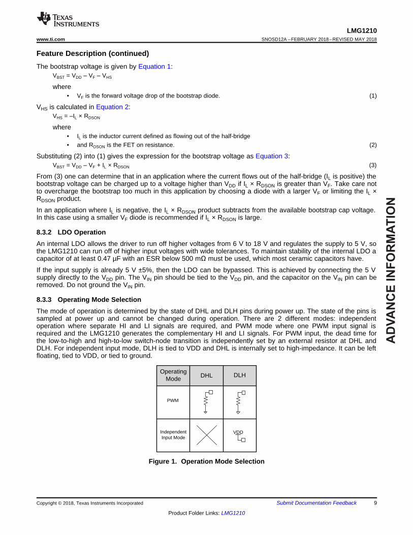
8.3.3 Operating Mode SelectionThe mode of operation is determined by the state of DHL and DLH pins during power up. The state of the pins issampled at power up and cannot be changed during operation. There are 2 different modes: independentoperation where separate HI and LI signals are required, and PWM mode where one PWM input signal isrequired and the LMG1210 generates the complementary HI and LI signals. For PWM input, the dead time forthe low-to-high and high-to-low switch-node transition is independently set by an external resistor at DHL andDLH. For independent input mode, DLH is tied to VDD and DHL is internally set to high-impedance. It can be leftfloating, tied to VDD, or tied to ground.
Figure 1. Operation Mode Selection

AD
VA
NC
E IN
FO
RM
AT
ION
10
LMG1210SNOSD12A –FEBRUARY 2018–REVISED MAY 2018 www.ti.com
Product Folder Links: LMG1210
Submit Documentation Feedback Copyright © 2018, Texas Instruments Incorporated
Feature Description (continued)8.3.4 Dead Time SelectionIn PWM mode the dead time can be set with a resistor placed between DHL/DLH and VSS. For a desired deadtime (tdt), the corresponding required resistance can be calculated in Equation 4 with tdt in ns and R in kΩ.
R = (900/tdt ) – 25 (4)
The maximum delay is 20 ns, which gives a minimum resistor value of 20 kΩ. It is acceptable to leave DHL andDLH floating if zero dead time is desired.
Using no dead time can result in shoot-through in some applications.
Before being used to generate the dead times, the voltages on the DHL and DLH pins are first filtered through aninternal RC filter with a nominal corner frequency of 10 kHz to attenuate switching noise.
8.3.5 Overtemperature ProtectionThe LMG1210 has three separate overtemperature thresholds: two on the low-side and one on the high-side.The lowest overtemperature threshold is the low-side switching threshold at 165 degrees typical. Whenexceeded, this disables switching on both the low and high sides. However, the 5 V LDO continues to operate.
If the low-side temperature continues to rise, that is, due to a short or external load on the 5 V LDO, then at 175degrees the low-side shuts down the 5 V LDO.
The high-side has an independent overtemperature threshold at 175 typical. When triggered, it only shuts off thehigh-side while the low-side may continue to operate.
If it is undesirable in an application to have only the high side shut off and not the low side, TI recommendsdesigning the thermal cooling of the board in a way to make the low-side die hotter. This can be achieved bycontrolling the size of the thermal planes connected to each DAP.
8.3.6 High-Performance Level ShifterThe LMG1210 uses a high-performance level shifter to translate the signal from the low side to the high side.The level shifter is built using TI's proprietary high-voltage capacitor technology, which showcase best-in-classCMTI (common-mode transient immunity). The level shifter can handle very high CMT (common-mode transient)rates while simultaneously providing low propagation time which does not vary depending on CMT rate.
8.4 Device Functional ModesTable 1 lists the functional modes for the LMG1210.
Table 1. LMG1210 Truth TableINPUTS PWM MODE INDEPENDENT MODE
EN/HI PWM/LI HO LO HO LO0 0 0 0 0 00 1 0 0 0 11 0 0 1 1 01 1 1 0 1 1

AD
VA
NC
E I
NF
OR
MA
TIO
N
LDO
HB
BST
VIN
EN/HI
PWM/LIDead Time
DHL DLH
6 ± 18 V
0 ± 200 V
HO
HS
5 VVDD
LO
VSS
Controller
LMG1210
Copyright © 2018, Texas Instruments Incorporated
11
LMG1210www.ti.com SNOSD12A –FEBRUARY 2018–REVISED MAY 2018
Product Folder Links: LMG1210
Submit Documentation FeedbackCopyright © 2018, Texas Instruments Incorporated
9 Application and Implementation
NOTEInformation in the following applications sections is not part of the TI componentspecification, and TI does not warrant its accuracy or completeness. TI’s customers areresponsible for determining suitability of components for their purposes. Customers shouldvalidate and test their design implementation to confirm system functionality.
9.1 Application InformationThe LMG1210 is designed to optimally drive GaN FETs in half-bridge configurations, such as synchronous buckand boost converters, as well as more complex topologies. By integrating the level shifting and bootstrapoperation the complexities of driving the high-side device are solved for the designer.
The list below shows some samples values for a typical 48 V to 12 V application synchronous buck.
• Input Voltage: 48 V• Output current: 10 A• Duty Cycle: 25 %• Bias voltage: 6 V• Duty Cycle: 25 %• Switching frequency: 1 MHz• Inductor: 4.7 µH
9.2 Typical Application
Figure 2. Simplified LMG1210 Configured as Synchronous Buck Converter

AD
VA
NC
E IN
FO
RM
AT
ION
12
LMG1210SNOSD12A –FEBRUARY 2018–REVISED MAY 2018 www.ti.com
Product Folder Links: LMG1210
Submit Documentation Feedback Copyright © 2018, Texas Instruments Incorporated
Typical Application (continued)9.2.1 Design RequirementsWhen designing a multi-MHz application that incorporates the LMG1210 gate driver and GaN power FETs, somedesign considerations must be evaluated first to make the most appropriate selection. Among theseconsiderations are layout optimization, circuit voltages, passive components, operating frequency, and controllerselection.
9.2.2 Detailed Design Procedure
9.2.2.1 Bypass CapacitorTo properly drive the GaN FETs, TI recommends placing high-quality ceramic bypass capacitors as close aspossible between the HB to HS and VDD to VSS. If using the LDO, the VDD-GND capacitor is required to be atleast 0.47 µF for stability. However, a larger capacitor may be required for many applications.
The bootstrap capacitor must be large enough to support charging the high-side FET and supplying the high-sidequiescent current when the high-side FET is on. The required capacitance can be calculated as Equation 5:
(QRR + QgH + IHB × ton)/ΔV = CBST,min
where• QgH is the gate charge of the high-side GaN FET,• IHB is the quiescent current of the high-side driver,• tON is the maximum on time period of the high side,• Qrr is the reverse recovery of the bootstrap diode• and ΔV is the acceptable droop on the bootstrap capacitor voltage. (5)
When using larger bootstrap capacitors, TI recommends that the VDD-VSS capacitor also be increased to keepthe ratio at least 5 to 1. If this is not maintained, the charging of the bootstrap capacitor can pull the VDD-VSS raildown sufficiently to cause UVLO conditions and potentially unwanted behavior.
9.2.2.2 Bootstrap Diode SelectionThe bootstrap diode blocks the high voltage from the gate drive circuitry when the switch node swings high, withthe rated blocking voltage equal to the maximum Vds of the GaN FET. For low or moderate frequency operationultra-fast recovery diodes (<50 ns) are recommended. The internal low voltage switch in the LMG1210 acts toreduce the reverse recovery. For high-frequency operation a Schottky diode is recommended. To minimizeswitching losses and improve performance, it is important to select a diode with low capacitance.
For extreme cases, where the low-side FET on time is less than 20 ns, TI recommends using a small GaN FETas synchronous bootstrap instead of a diode. In this case, TI recommends leaving the BST pin floating orconnected to VDD, and to connect the source of the synchronous bootstrap directly to VDD.
9.2.2.3 Handling Ground BounceFor the best switching performance, it is important to connect the VSS gate return to the source of the low-sideFET with a very low-inductance path.
However, doing so can cause the ground of the LMG1210 to bounce relative to the system or controller groundand cause erroneous switching transitions on the inputs. Multiple strategies can be employed to eliminate theseundesired transitions.
The LMG1210 has input hysteresis built into the input buffers to help counteract this effect, but this alone maynot be sufficient in all applications. The simplest option is to tie the system ground together and the powerground only at the LMG1210 (single-point connection). This gives the cleanest solution but may not always bepossible depending on system grounding requirements.
For moderate ground-bounce cases, a simple R-C filter can be built with a simple resistor in series with theinputs. The resistor should be close to the inputs of the LMG1210. The input capacitance of the LMG1210produces an RC filter which can help decrease ringing at the inputs. The addition of a small C on the inputs tosupplement the LMG1210 input capacitance can also be helpful. This solution is acceptable for moderate casesin applications where the extra delay is acceptable.

AD
VA
NC
E I
NF
OR
MA
TIO
N
Rsense
Vsense
Controller
Filter
LDO
HB
BST
VIN
EN/HI
PWM/LIDead Time
DHL DLH
6 ± 18 V
0 ± 200 V
HO
HS
5 VVDD
LO
VSS
LMG1210
Copyright © 2018, Texas Instruments Incorporated
13
LMG1210www.ti.com SNOSD12A –FEBRUARY 2018–REVISED MAY 2018
Product Folder Links: LMG1210
Submit Documentation FeedbackCopyright © 2018, Texas Instruments Incorporated
Typical Application (continued)For more extreme cases or where no delay is tolerable, using a common-mode choke provides the best results.One example application where the ground bounce is particularly challenging is when using a current senseresistor. In this application, the LMG1210 ground is connected to the GaN source, while the controller ground isconnected to the other side of the current sense resistor as shown in Figure 3.
Figure 3. LMG1210 Configured With Current Sense Resistor Using a CMC as Filter
The combination of high dI/dt experienced through the sense resistor inductance will cause severe ground noisethat could cause false triggering or even damage the part. To prevent this, a common-mode choke (CMC) can beused. Each signal requires its own CMC. Also, to provide additional RC filtering, a 100 Ω resistor should beadded to the signal output line before the LMG1210.
9.2.2.4 Independent Input ModeIn independent input mode, the signals LI and HI will propagate to the outputs LO and HO maintaining the samephase shift, varied only by the timing mismatch.
In this mode, the dead time-generating circuit will be inoperative, and the correct dead time value would have tobe generated by the controller.
The controller is responsible for assuring that the LI and HI on-times do not overlap and cause shoot-through.
9.2.2.5 Computing Power DissipationThe power dissipation of the LMG1210 can be divided up into three constituent parts. One is the quiescentcurrent which is defined in the Electrical Characteristics table. This is the current consumed when no switching istaking place.
The second is the dynamic power consumed in the internal circuits of the driver at each switching transitionregardless of the load on the output. This can be measured by switching the driver with no output load.
The third component is the power used to switch the load capacitance presented by the external FET.
If operating in PWM mode, there is an additional quiescent current consumed in the dead time resistors. Theadditional current consumed in each dead time pin can be calculated as Equation 6.
Iqdxx = 1.8/(25k + Rext) (6)

AD
VA
NC
E IN
FO
RM
AT
ION
14
LMG1210SNOSD12A –FEBRUARY 2018–REVISED MAY 2018 www.ti.com
Product Folder Links: LMG1210
Submit Documentation Feedback Copyright © 2018, Texas Instruments Incorporated
Typical Application (continued)The first component, the quiescent power, is given in the Electrical Characteristics table. The second component,the dynamic power dissipation can be calculated as Equation 7.
IINT = IDYN × Fsw
where• IDYN is the dynamic current consumption found in the Electrical Characteristics table• and Fsw is the switching frequency. (7)
The third component of the power dissipation is the gate driver power. The current associated to this loss can becalculated given the Qg of the FET as Equation 8:
I FET,g= Qg × Fsw (8)
or alternatively in terms of Ciss as Equation 9:IFET,g = Ciss × Vsup × Fsw (9)
These current consumption numbers should be calculated for both the high side and low side separately andadded together. When a total current consumption is computed, multiplying it by the input supply voltage gives aworst-case approximation for the total power dissipation of the LMG1210. If using a non-zero external gateresistor of value Rg,ext, some of this power will be dissipated in this external resistor, and can be subtracted fromthe power consumed inside the IC.
The WQFN package has two thermal pads: one for the low-side die and another for the high-side die. Thoughthere is good thermal coupling between the die and the associated thermal pad, there is very limited thermalcoupling between a die and the opposite thermal pad. This means that if power dissipation calculations indicate adie needs improved cooling, the cooling must be focused on cooling the correct thermal pad.
9.3 Do's and Don'tsWhen using the LMG1210, DO:1. Read and fully understand the data sheet, including the application notes and layout recommendations.2. Use a four-layer board and place the return power path on an inner layer to minimize power-loop inductance.3. Use small, surface-mount bypass and bus capacitors to minimize parasitic inductance.4. Use the proper size decoupling capacitors and place them close to the IC as described in the Layout
Guidelines section.5. Use common-mode chokes for the input signals to reduce ground bounce noise. If not, ensure the signal
source is connected to the signal GND plane which is tied to the power source only at the LMG1210 IC.
To avoid issues in your system when using the LMG1210, DON'T:1. Use a single-layer or two-layer PCB for the LMG1210 as the power-loop and bypass capacitor inductances
will be excessive and prevent proper operation of the IC.2. Reduce the bypass capacitor values below the recommended values.3. Allow the device to experience pin transients above 300 V as they may damage the device.4. Drive the IC from a controller with a separate ground connection than the GND pin of the IC, unless
connecting though a CMC.

AD
VA
NC
E I
NF
OR
MA
TIO
N
15
LMG1210www.ti.com SNOSD12A –FEBRUARY 2018–REVISED MAY 2018
Product Folder Links: LMG1210
Submit Documentation FeedbackCopyright © 2018, Texas Instruments Incorporated
10 Power Supply RecommendationsThe power to the LMG1210 can be supplied either through the LDO or the LDO can be bypassed and 5 V canbe supplied directly. The maximum input voltage to the LDO of the LMG1210 is specified in the electricalcharacteristics table. The minimum input of the LDO is set by the minimum drop-out of the LDO at theoperational current. The dropout at max current is specified in the electrical characteristics table, but a lowerdropout can be used in a lower-current application. A local bypass capacitor must be placed between the VIN andGND pins, and the VDD and GND pins. This capacitor must be placed as close as possible to the device. TIrecommends a low-ESR, ceramic, surface-mount capacitor. TI also recommends using 2 capacitors across VDDand GND pin: a 100 nF ceramic surface-mount capacitor for high frequency filtering placed very close to VDD andGND pin, and another surface-mount capacitor, 220 nF to 10 μF, for IC bias requirement. The VIN and GNDcapacitor can be removed if the LDO is bypassed.
11 Layout
11.1 Layout GuidelinesThe layout of the LMG1210 is critical for performance and functionality. The low inductance WQFN packagehelps mitigate many of the problems associated with board level parasitics, but take care with layout andplacement with components to insure proper operation. The following design rules are recommended.• Place LMG1210 as close to the GaN FETs as possible to minimize the length of high-current traces between
the HO/LO and the Gate of the GaN FETs• Place bootstrap diode as close as possible to the LMG1210 to minimize the inductance of the BST to HB
loop.• Place the bypass capacitors across VIN to VSS, VDD to VSS, and HB to HS as close to the LMG1210 pins
as possible. The VDD to VSS cap is a higher priority than the VIN to VSS cap.• Separate power traces and signal traces, such as output and input signals, and minimize any overlaps
between layers• Minimize capacitance from the high-side pins to the input pins to minimize noise injection.

AD
VA
NC
E IN
FO
RM
AT
ION
16
LMG1210SNOSD12A –FEBRUARY 2018–REVISED MAY 2018 www.ti.com
Product Folder Links: LMG1210
Submit Documentation Feedback Copyright © 2018, Texas Instruments Incorporated
11.2 Layout Example
Figure 4. LMG1210 Layout Example

AD
VA
NC
E I
NF
OR
MA
TIO
N
17
LMG1210www.ti.com SNOSD12A –FEBRUARY 2018–REVISED MAY 2018
Product Folder Links: LMG1210
Submit Documentation FeedbackCopyright © 2018, Texas Instruments Incorporated
12 Device and Documentation Support
12.1 Documentation Support
12.1.1 Related DocumentationFor related documentation see the following:• Dead Time Optimization for the LMG1210 Half-Bridge GaN Driver (SNVA815)• LMG1210 TINA-TI Reference Design (SNOM617)• LMG1210 TINA-TI Transient Spice Model (SNOM616)• LMG1210 PSpice Transient Model (SNOM615)
12.2 Receiving Notification of Documentation UpdatesTo receive notification of documentation updates, navigate to the device product folder on ti.com. In the upperright corner, click on Alert me to register and receive a weekly digest of any product information that haschanged. For change details, review the revision history included in any revised document.
12.3 Community ResourcesThe following links connect to TI community resources. Linked contents are provided "AS IS" by the respectivecontributors. They do not constitute TI specifications and do not necessarily reflect TI's views; see TI's Terms ofUse.
TI E2E™ Online Community TI's Engineer-to-Engineer (E2E) Community. Created to foster collaborationamong engineers. At e2e.ti.com, you can ask questions, share knowledge, explore ideas and helpsolve problems with fellow engineers.
Design Support TI's Design Support Quickly find helpful E2E forums along with design support tools andcontact information for technical support.
12.4 TrademarksE2E is a trademark of Texas Instruments.All other trademarks are the property of their respective owners.
12.5 Electrostatic Discharge CautionThis integrated circuit can be damaged by ESD. Texas Instruments recommends that all integrated circuits be handled withappropriate precautions. Failure to observe proper handling and installation procedures can cause damage.
ESD damage can range from subtle performance degradation to complete device failure. Precision integrated circuits may be moresusceptible to damage because very small parametric changes could cause the device not to meet its published specifications.
12.6 GlossarySLYZ022 — TI Glossary.
This glossary lists and explains terms, acronyms, and definitions.
13 Mechanical, Packaging, and Orderable InformationThe following pages include mechanical, packaging, and orderable information. This information is the mostcurrent data available for the designated devices. This data is subject to change without notice and revision ofthis document. For browser-based versions of this data sheet, refer to the left-hand navigation.
LMG1210 is released as MSL3. Products that exceed their floor life can be re-worked with a bake to drive outresidual moisture. IPC/JEDEC J-STD-033C provides guidance about the baking procedure and where youshould take care to ensure that the plastic housing (trays, tape and reel or tubes) can withstand the temperaturesbeing considered.

PACKAGE OPTION ADDENDUM
www.ti.com 5-Apr-2018
Addendum-Page 1
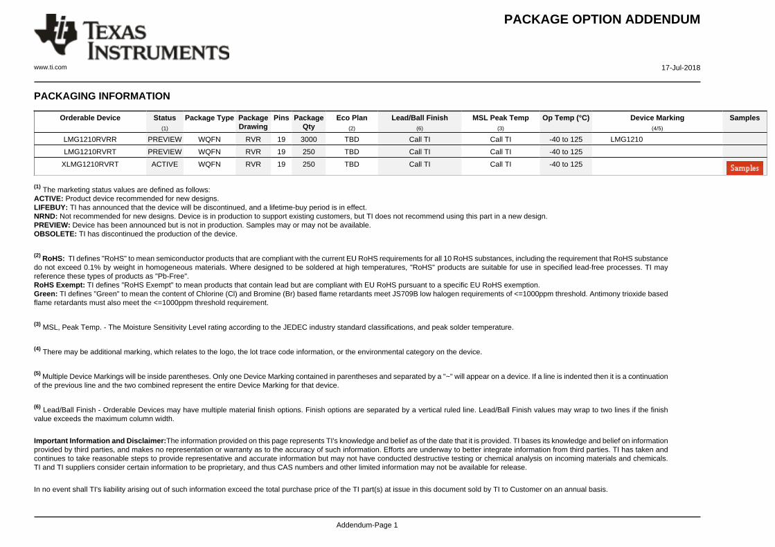
PACKAGING INFORMATION
Orderable Device Status(1)
Package Type PackageDrawing
Pins PackageQty
Eco Plan(2)
Lead/Ball Finish(6)
MSL Peak Temp(3)
Op Temp (°C) Device Marking(4/5)
Samples
LMG1210RVRR PREVIEW WQFN RVR 19 3000 TBD Call TI Call TI -40 to 125
LMG1210RVRT PREVIEW WQFN RVR 19 250 TBD Call TI Call TI -40 to 125
XLMG1210RVRT ACTIVE WQFN RVR 19 250 TBD Call TI Call TI -40 to 125
(1) The marketing status values are defined as follows:ACTIVE: Product device recommended for new designs.LIFEBUY: TI has announced that the device will be discontinued, and a lifetime-buy period is in effect.NRND: Not recommended for new designs. Device is in production to support existing customers, but TI does not recommend using this part in a new design.PREVIEW: Device has been announced but is not in production. Samples may or may not be available.OBSOLETE: TI has discontinued the production of the device.
(2) RoHS: TI defines "RoHS" to mean semiconductor products that are compliant with the current EU RoHS requirements for all 10 RoHS substances, including the requirement that RoHS substancedo not exceed 0.1% by weight in homogeneous materials. Where designed to be soldered at high temperatures, "RoHS" products are suitable for use in specified lead-free processes. TI mayreference these types of products as "Pb-Free".RoHS Exempt: TI defines "RoHS Exempt" to mean products that contain lead but are compliant with EU RoHS pursuant to a specific EU RoHS exemption.Green: TI defines "Green" to mean the content of Chlorine (Cl) and Bromine (Br) based flame retardants meet JS709B low halogen requirements of <=1000ppm threshold. Antimony trioxide basedflame retardants must also meet the <=1000ppm threshold requirement.
(3) MSL, Peak Temp. - The Moisture Sensitivity Level rating according to the JEDEC industry standard classifications, and peak solder temperature.
(4) There may be additional marking, which relates to the logo, the lot trace code information, or the environmental category on the device.
(5) Multiple Device Markings will be inside parentheses. Only one Device Marking contained in parentheses and separated by a "~" will appear on a device. If a line is indented then it is a continuationof the previous line and the two combined represent the entire Device Marking for that device.
(6) Lead/Ball Finish - Orderable Devices may have multiple material finish options. Finish options are separated by a vertical ruled line. Lead/Ball Finish values may wrap to two lines if the finishvalue exceeds the maximum column width.
Important Information and Disclaimer:The information provided on this page represents TI's knowledge and belief as of the date that it is provided. TI bases its knowledge and belief on informationprovided by third parties, and makes no representation or warranty as to the accuracy of such information. Efforts are underway to better integrate information from third parties. TI has taken andcontinues to take reasonable steps to provide representative and accurate information but may not have conducted destructive testing or chemical analysis on incoming materials and chemicals.TI and TI suppliers consider certain information to be proprietary, and thus CAS numbers and other limited information may not be available for release.
In no event shall TI's liability arising out of such information exceed the total purchase price of the TI part(s) at issue in this document sold by TI to Customer on an annual basis.

www.ti.com
PACKAGE OUTLINE
C
A A
19X 0.30.2
1.2±0.1
19X 0.50.3
0.8 MAX
(0.2) TYP
0.050.00
13X 0.5
2X2
2X1.7 0.1
2X 2.5
0.75±0.1
4X 1.25
(0.75) (0.975)
A 4.13.9
B
3.12.9
(0.1)
(0.05)
(0.75)
WQFN - 0.8 mm max heightRVR0019APLASTIC QUAD FLATPACK - NO LEAD
4222723/B 04/2016
PIN 1 INDEX AREA
SEATING PLANE
0.08 C
1
5 11
15
6 10
19 16
(OPTIONAL)PIN 1 ID 0.1 C A B
0.05
THERMAL PAD2X EXPOSED
PKG
SYMM20 21
NOTES: 1. All linear dimensions are in millimeters. Any dimensions in parenthesis are for reference only. Dimensioning and tolerancing per ASME Y14.5M. 2. This drawing is subject to change without notice. 3. The package thermal pad must be soldered to the printed circuit board for thermal and mechanical performance.
SCALE 3.500
SCALE 25.000SECTION A-ASECTION A-ATYPICAL

www.ti.com
EXAMPLE BOARD LAYOUT
0.05 MINALL AROUND
0.05 MAXALL AROUND
19X (0.25)
19X (0.6) ( ) TYPVIA
0.2
(R ) TYP0.05
4X(0.6)
(2.8)
(3.8)
13X (0.5)
(1.2)
2X(1.7)
(0.75)
(0.75) (0.975)
2X (1.25) 2X (1.25)
WQFN - 0.8 mm max heightRVR0019APLASTIC QUAD FLATPACK - NO LEAD
4222723/B 04/2016
PKG
1
5
6 10
11
15
1619
SYMM
LAND PATTERN EXAMPLESCALE:18X
20 21
NOTES: (continued) 4. This package is designed to be soldered to a thermal pad on the board. For more information, see Texas Instruments literature number SLUA271 (www.ti.com/lit/slua271).5. Vias are optional depending on application, refer to device data sheet. If any vias are implemented, refer to their locations shown on this view. It is recommended that vias under paste be filled, plugged or tented.
SOLDER MASKOPENING
METAL UNDERSOLDER MASK
SOLDER MASKDEFINED
METAL
SOLDER MASKOPENING
SOLDER MASK DETAILS
NON SOLDER MASKDEFINED
(PREFERRED)

www.ti.com
EXAMPLE STENCIL DESIGN
19X (0.6)
19X (0.25)
13X (0.5)
(3.8)
(2.8)
(R ) TYP0.05
4X(0.475)
2X (0.75) 2X (0.975)
2X (1.13)
2X (0.71)
4X(0.75)
2X (1.25) 2X (1.25)
WQFN - 0.8 mm max heightRVR0019APLASTIC QUAD FLATPACK - NO LEAD
4222723/B 04/2016
NOTES: (continued) 6. Laser cutting apertures with trapezoidal walls and rounded corners may offer better paste release. IPC-7525 may have alternate design recommendations.
PKG
METALTYP
SOLDER PASTE EXAMPLEBASED ON 0.125 mm THICK STENCIL
EXPOSED PADS 20 & 21:
83% PRINTED SOLDER COVERAGE BY AREASCALE:25X
SYMM
1
5
6 10
11
15
1619
2021
PACKAGE OPTION ADDENDUM
www.ti.com 17-Jul-2018
Addendum-Page 1
PACKAGING INFORMATION
Orderable Device Status(1)
Package Type PackageDrawing
Pins PackageQty
Eco Plan(2)
Lead/Ball Finish(6)
MSL Peak Temp(3)
Op Temp (°C) Device Marking(4/5)
Samples
LMG1210RVRR PREVIEW WQFN RVR 19 3000 TBD Call TI Call TI -40 to 125 LMG1210
LMG1210RVRT PREVIEW WQFN RVR 19 250 TBD Call TI Call TI -40 to 125
XLMG1210RVRT ACTIVE WQFN RVR 19 250 TBD Call TI Call TI -40 to 125
(1) The marketing status values are defined as follows:ACTIVE: Product device recommended for new designs.LIFEBUY: TI has announced that the device will be discontinued, and a lifetime-buy period is in effect.NRND: Not recommended for new designs. Device is in production to support existing customers, but TI does not recommend using this part in a new design.PREVIEW: Device has been announced but is not in production. Samples may or may not be available.OBSOLETE: TI has discontinued the production of the device.
(2) RoHS: TI defines "RoHS" to mean semiconductor products that are compliant with the current EU RoHS requirements for all 10 RoHS substances, including the requirement that RoHS substancedo not exceed 0.1% by weight in homogeneous materials. Where designed to be soldered at high temperatures, "RoHS" products are suitable for use in specified lead-free processes. TI mayreference these types of products as "Pb-Free".RoHS Exempt: TI defines "RoHS Exempt" to mean products that contain lead but are compliant with EU RoHS pursuant to a specific EU RoHS exemption.Green: TI defines "Green" to mean the content of Chlorine (Cl) and Bromine (Br) based flame retardants meet JS709B low halogen requirements of <=1000ppm threshold. Antimony trioxide basedflame retardants must also meet the <=1000ppm threshold requirement.
(3) MSL, Peak Temp. - The Moisture Sensitivity Level rating according to the JEDEC industry standard classifications, and peak solder temperature.
(4) There may be additional marking, which relates to the logo, the lot trace code information, or the environmental category on the device.
(5) Multiple Device Markings will be inside parentheses. Only one Device Marking contained in parentheses and separated by a "~" will appear on a device. If a line is indented then it is a continuationof the previous line and the two combined represent the entire Device Marking for that device.
(6) Lead/Ball Finish - Orderable Devices may have multiple material finish options. Finish options are separated by a vertical ruled line. Lead/Ball Finish values may wrap to two lines if the finishvalue exceeds the maximum column width.
Important Information and Disclaimer:The information provided on this page represents TI's knowledge and belief as of the date that it is provided. TI bases its knowledge and belief on informationprovided by third parties, and makes no representation or warranty as to the accuracy of such information. Efforts are underway to better integrate information from third parties. TI has taken andcontinues to take reasonable steps to provide representative and accurate information but may not have conducted destructive testing or chemical analysis on incoming materials and chemicals.TI and TI suppliers consider certain information to be proprietary, and thus CAS numbers and other limited information may not be available for release.
In no event shall TI's liability arising out of such information exceed the total purchase price of the TI part(s) at issue in this document sold by TI to Customer on an annual basis.

IMPORTANT NOTICE
Texas Instruments Incorporated (TI) reserves the right to make corrections, enhancements, improvements and other changes to itssemiconductor products and services per JESD46, latest issue, and to discontinue any product or service per JESD48, latest issue. Buyersshould obtain the latest relevant information before placing orders and should verify that such information is current and complete.TI’s published terms of sale for semiconductor products (http://www.ti.com/sc/docs/stdterms.htm) apply to the sale of packaged integratedcircuit products that TI has qualified and released to market. Additional terms may apply to the use or sale of other types of TI products andservices.Reproduction of significant portions of TI information in TI data sheets is permissible only if reproduction is without alteration and isaccompanied by all associated warranties, conditions, limitations, and notices. TI is not responsible or liable for such reproduceddocumentation. Information of third parties may be subject to additional restrictions. Resale of TI products or services with statementsdifferent from or beyond the parameters stated by TI for that product or service voids all express and any implied warranties for theassociated TI product or service and is an unfair and deceptive business practice. TI is not responsible or liable for any such statements.Buyers and others who are developing systems that incorporate TI products (collectively, “Designers”) understand and agree that Designersremain responsible for using their independent analysis, evaluation and judgment in designing their applications and that Designers havefull and exclusive responsibility to assure the safety of Designers' applications and compliance of their applications (and of all TI productsused in or for Designers’ applications) with all applicable regulations, laws and other applicable requirements. Designer represents that, withrespect to their applications, Designer has all the necessary expertise to create and implement safeguards that (1) anticipate dangerousconsequences of failures, (2) monitor failures and their consequences, and (3) lessen the likelihood of failures that might cause harm andtake appropriate actions. Designer agrees that prior to using or distributing any applications that include TI products, Designer willthoroughly test such applications and the functionality of such TI products as used in such applications.TI’s provision of technical, application or other design advice, quality characterization, reliability data or other services or information,including, but not limited to, reference designs and materials relating to evaluation modules, (collectively, “TI Resources”) are intended toassist designers who are developing applications that incorporate TI products; by downloading, accessing or using TI Resources in anyway, Designer (individually or, if Designer is acting on behalf of a company, Designer’s company) agrees to use any particular TI Resourcesolely for this purpose and subject to the terms of this Notice.TI’s provision of TI Resources does not expand or otherwise alter TI’s applicable published warranties or warranty disclaimers for TIproducts, and no additional obligations or liabilities arise from TI providing such TI Resources. TI reserves the right to make corrections,enhancements, improvements and other changes to its TI Resources. TI has not conducted any testing other than that specificallydescribed in the published documentation for a particular TI Resource.Designer is authorized to use, copy and modify any individual TI Resource only in connection with the development of applications thatinclude the TI product(s) identified in such TI Resource. NO OTHER LICENSE, EXPRESS OR IMPLIED, BY ESTOPPEL OR OTHERWISETO ANY OTHER TI INTELLECTUAL PROPERTY RIGHT, AND NO LICENSE TO ANY TECHNOLOGY OR INTELLECTUAL PROPERTYRIGHT OF TI OR ANY THIRD PARTY IS GRANTED HEREIN, including but not limited to any patent right, copyright, mask work right, orother intellectual property right relating to any combination, machine, or process in which TI products or services are used. Informationregarding or referencing third-party products or services does not constitute a license to use such products or services, or a warranty orendorsement thereof. Use of TI Resources may require a license from a third party under the patents or other intellectual property of thethird party, or a license from TI under the patents or other intellectual property of TI.TI RESOURCES ARE PROVIDED “AS IS” AND WITH ALL FAULTS. TI DISCLAIMS ALL OTHER WARRANTIES ORREPRESENTATIONS, EXPRESS OR IMPLIED, REGARDING RESOURCES OR USE THEREOF, INCLUDING BUT NOT LIMITED TOACCURACY OR COMPLETENESS, TITLE, ANY EPIDEMIC FAILURE WARRANTY AND ANY IMPLIED WARRANTIES OFMERCHANTABILITY, FITNESS FOR A PARTICULAR PURPOSE, AND NON-INFRINGEMENT OF ANY THIRD PARTY INTELLECTUALPROPERTY RIGHTS. TI SHALL NOT BE LIABLE FOR AND SHALL NOT DEFEND OR INDEMNIFY DESIGNER AGAINST ANY CLAIM,INCLUDING BUT NOT LIMITED TO ANY INFRINGEMENT CLAIM THAT RELATES TO OR IS BASED ON ANY COMBINATION OFPRODUCTS EVEN IF DESCRIBED IN TI RESOURCES OR OTHERWISE. IN NO EVENT SHALL TI BE LIABLE FOR ANY ACTUAL,DIRECT, SPECIAL, COLLATERAL, INDIRECT, PUNITIVE, INCIDENTAL, CONSEQUENTIAL OR EXEMPLARY DAMAGES INCONNECTION WITH OR ARISING OUT OF TI RESOURCES OR USE THEREOF, AND REGARDLESS OF WHETHER TI HAS BEENADVISED OF THE POSSIBILITY OF SUCH DAMAGES.Unless TI has explicitly designated an individual product as meeting the requirements of a particular industry standard (e.g., ISO/TS 16949and ISO 26262), TI is not responsible for any failure to meet such industry standard requirements.Where TI specifically promotes products as facilitating functional safety or as compliant with industry functional safety standards, suchproducts are intended to help enable customers to design and create their own applications that meet applicable functional safety standardsand requirements. Using products in an application does not by itself establish any safety features in the application. Designers mustensure compliance with safety-related requirements and standards applicable to their applications. Designer may not use any TI products inlife-critical medical equipment unless authorized officers of the parties have executed a special contract specifically governing such use.Life-critical medical equipment is medical equipment where failure of such equipment would cause serious bodily injury or death (e.g., lifesupport, pacemakers, defibrillators, heart pumps, neurostimulators, and implantables). Such equipment includes, without limitation, allmedical devices identified by the U.S. Food and Drug Administration as Class III devices and equivalent classifications outside the U.S.TI may expressly designate certain products as completing a particular qualification (e.g., Q100, Military Grade, or Enhanced Product).Designers agree that it has the necessary expertise to select the product with the appropriate qualification designation for their applicationsand that proper product selection is at Designers’ own risk. Designers are solely responsible for compliance with all legal and regulatoryrequirements in connection with such selection.Designer will fully indemnify TI and its representatives against any damages, costs, losses, and/or liabilities arising out of Designer’s non-compliance with the terms and provisions of this Notice.
Mailing Address: Texas Instruments, Post Office Box 655303, Dallas, Texas 75265Copyright © 2018, Texas Instruments Incorporated