li-ion linear battery charger with ldo · battery floating voltage 4.158i bat = 1 ma 4.2 4.242 v i...
TRANSCRIPT
December 2017 DocID024654 Rev 4 1/29
This is information on a product in full production. www.st.com
STNS01
Li-Ion linear battery charger with LDO
Datasheet - production data
Features Charges single-cell Li-Ion batteries with
CC/CV algorithm and charge termination
Charge current programmable up to 200 mA
1% accuracy on floating voltage (4.2 V)
Integrated 3.1 V LDO regulator
Automatic power path management
Battery overcharge protection
Battery over-discharge protection
Battery overcurrent protection
Charging timeout
Very low battery leakage in over-discharge/shutdown mode
Low quiescent current
Charge/fault status output
Charger enable input
Available in a DFN12L (3x3x0.75 mm) package
Applications Portable MP3 players
Portable low-power devices
Fitness portable devices
Description The STNS01 is a linear charger for single-cell Li-Ion batteries integrating an LDO regulator and several battery protection functions.
The STNS01 uses a CC/CV algorithm to charge the battery; the fast-charge current can be programmed using an external resistor. Pre-charge current and termination current are scaled accordingly. The floating voltage value is 4.2 V.
The input supply voltage is normally used to charge the battery and provide power to the LDO regulator. When a valid input voltage is not present and the battery is not empty, the device automatically switches to battery power.
The STNS01 integrates overcharge, over-discharge and overcurrent protection circuitry to prevent the battery from being damaged under fault conditions. It also features a charger enable input to stop the charging process when battery overtemperature is detected by an external circuitry.
When the shutdown mode is activated, the battery power consumption is reduced to less than 500 nA to maximize battery life during shelf time or shipping. The device is available in the DFN12L (3x3x0.75 mm) package.
Table 1: Device summary
Order code Package Packing
STNS01PUR DFN12L
(3x3x0.75 mm)
3000
parts per reel
Contents STNS01
2/29 DocID024654 Rev 4
Contents
1 Application schematic .................................................................... 6
2 Block diagram .................................................................................. 7
3 Pin configuration ............................................................................. 8
4 Maximum ratings ............................................................................. 9
5 Electrical characteristics .............................................................. 10
6 Typical performance characteristics (curves) ............................. 13
6.1 IN .................................................................................................... 15
6.2 SYS ................................................................................................. 15
6.3 LDO ................................................................................................. 15
6.4 SD ................................................................................................... 15
6.5 CHG ................................................................................................ 16
6.6 CEN ................................................................................................ 16
6.7 GND ................................................................................................ 17
6.8 NTC ................................................................................................. 17
6.9 ISET ................................................................................................ 17
6.10 BATMS ............................................................................................ 17
6.11 BATSNS .......................................................................................... 18
6.12 BAT ................................................................................................. 18
7 Operation description ................................................................... 19
7.1 Power-on ......................................................................................... 19
7.2 Battery charger ................................................................................ 19
7.3 Battery temperature monitoring ....................................................... 21
7.4 Battery overcharge protection ......................................................... 22
7.5 Battery over-discharge protection ................................................... 22
7.6 Battery discharge overcurrent protection ........................................ 22
7.7 Input overcurrent protection ............................................................ 22
7.8 SYS and LDO short-circuit protection ............................................. 23
7.9 IN overvoltage protection ................................................................ 23
7.10 Shutdown mode .............................................................................. 23
7.11 Thermal shutdown ........................................................................... 23
7.12 Reverse current protection .............................................................. 23
8 Package information ..................................................................... 24
STNS01 Contents
DocID024654 Rev 4 3/29
8.1 DFN12L (3x3x0.75 mm) package information ................................. 24
8.2 DFN12L (3x3x0.75 mm) packing information .................................. 26
9 Revision history ............................................................................ 28
List of tables STNS01
4/29 DocID024654 Rev 4
List of tables
Table 1: Device summary ........................................................................................................................... 1 Table 2: List of external components .......................................................................................................... 6 Table 3: Pin description .............................................................................................................................. 8 Table 4: Absolute maximum ratings ........................................................................................................... 9 Table 5: Thermal data ................................................................................................................................. 9 Table 6: Electrical characteristics ............................................................................................................. 10 Table 7: SYS pin voltage .......................................................................................................................... 15 Table 8: CHG pin state ............................................................................................................................. 16 Table 9: DFN12L (3x3x0.75 mm) package mechanical data ................................................................... 25 Table 10: Document revision history ........................................................................................................ 28
STNS01 List of figures
DocID024654 Rev 4 5/29
List of figures
Figure 1: STNS01 application schematic.................................................................................................... 6 Figure 2: STNS01 block diagram ................................................................................................................ 7 Figure 3: Pin configuration (top view) ......................................................................................................... 8 Figure 4: Start-up ...................................................................................................................................... 13 Figure 5: Start - up VBAT = 0 V ................................................................................................................ 13 Figure 6: Input OVP .................................................................................................................................. 13 Figure 7: IPRE-CHG to IFAST-CHG ......................................................................................................... 13 Figure 8: Plug USB ................................................................................................................................... 14 Figure 9: Unplug USB (battery powered).................................................................................................. 14 Figure 10: RON-BS vs. temperature ......................................................................................................... 14 Figure 11: Battery voltage vs. charge current ........................................................................................... 14 Figure 12: Load transient LDO pre-chg .................................................................................................... 14 Figure 13: Load transient LDO fast-chg.................................................................................................... 14 Figure 14: VLDO vs. temperature ............................................................................................................. 15 Figure 15: VLDO load static regulation ..................................................................................................... 15 Figure 16: Shutdown mode entry and exit (not to scale, deglitch times not included) ............................. 16 Figure 17: Charge disable / enable ........................................................................................................... 17 Figure 18: Charging flowchart ................................................................................................................... 20 Figure 19: CC-CV charging profile (not to scale) ...................................................................................... 21 Figure 20: Charging cycle profile .............................................................................................................. 21 Figure 21: Discharging cycle profile .......................................................................................................... 22 Figure 22: DFN12L (3x3x0.75 mm) package outline ................................................................................ 24 Figure 23: DFN12L (3x3x0.75 mm) recommended footprint .................................................................... 25 Figure 24: Tape outline ............................................................................................................................. 26 Figure 25: Reel outline .............................................................................................................................. 27
Application schematic STNS01
6/29 DocID024654 Rev 4
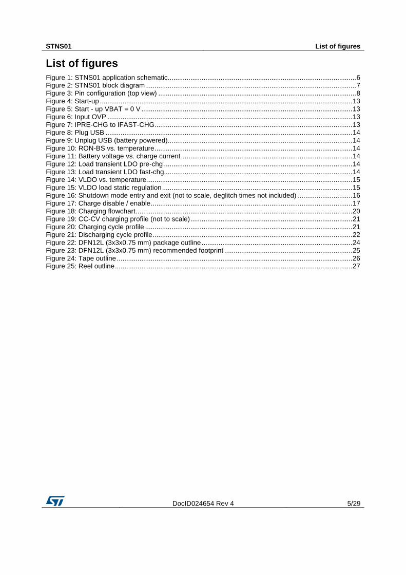
1 Application schematic Figure 1: STNS01 application schematic
Table 2: List of external components
Symbol Manufacturer Value Description Size
CIN Murata 2.2 µF GRM188R71A225KE15D
0603
CSYS Murata 2.2 µF GRM188R71A225KE15D
CLDO Murata 2.2 µF GRM188R71A225KE15D
RISET Any 1 kΩ – 13 kΩ Resistor
CBAT Murata 4.7 µF GRM188R61A475KE15D
D1 Any
Diode led
RDIV1, DIV2 Any
Depending on the BATMS status
RCHG Any 600 Ω Resistor
CLDO
2.2 µF GRM188R71A225KE15D
STNS01 Block diagram
DocID024654 Rev 4 7/29
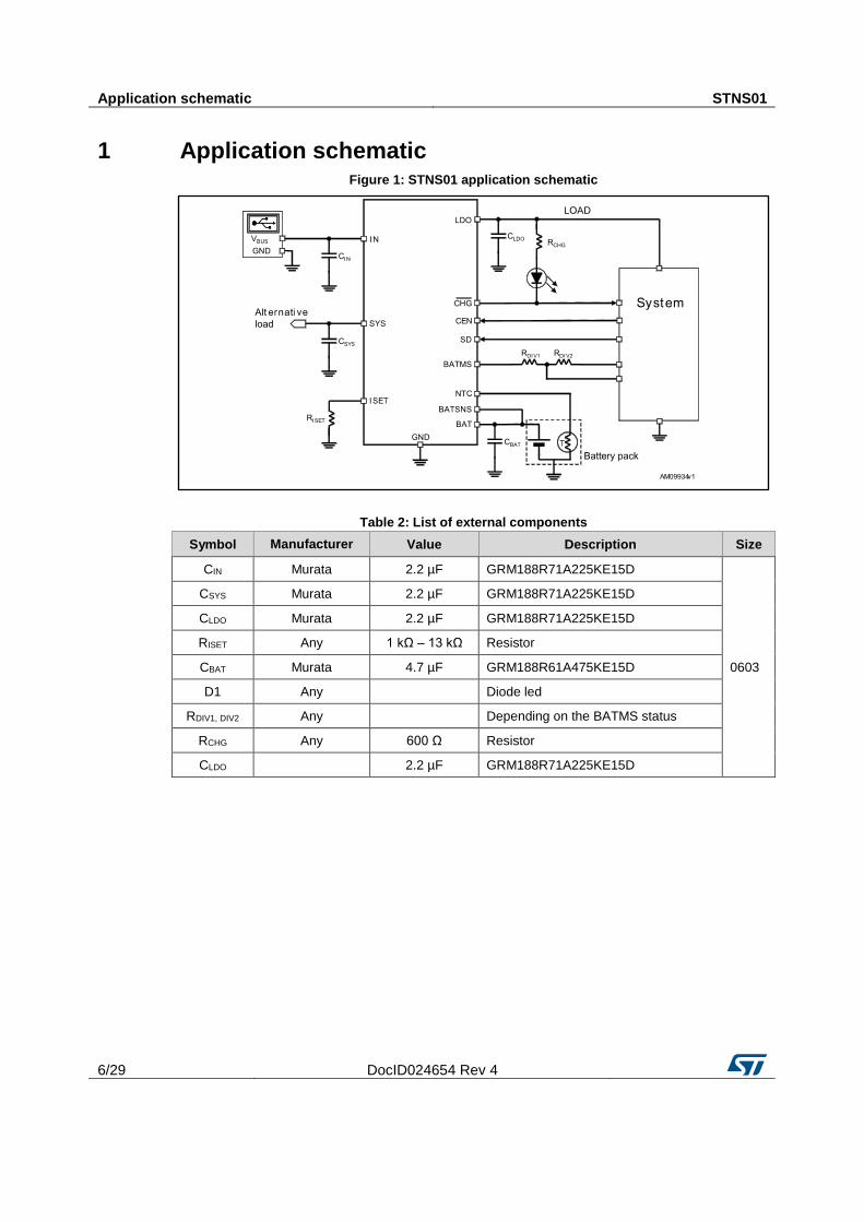
2 Block diagram Figure 2: STNS01 block diagram
Pin configuration STNS01
8/29 DocID024654 Rev 4
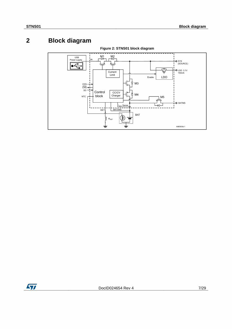
3 Pin configuration Figure 3: Pin configuration (top view)
Table 3: Pin description
Pin name Number Description
IN 1 Input supply voltage. Bypass this pin to ground with a 2.2 µF capacitor
SYS 2 System output. Bypass this pin to GND with a 2.2 µF ceramic capacitor
LDO 3 3.1 V LDO output. Bypass this pin to ground with a 1 μF ceramic capacitor
SD 4 Shutdown. Active high. 500 kΩ internal pull-down
CHG 5 Charging/fault flag. Active low
CEN 6 Charger enable pin. Active high. 500 kΩ internal pull-up (to LDO)
GND 7 Ground
NTC 8 Battery temperature monitor pin
ISET 9 Fast-charge programming resistor
BATMS 10 Battery voltage measurement pin
BATSNS 11 Battery voltage sensing. Connect as close as possible to the battery positive terminal
BAT 12 Battery positive terminal. Bypass this pin to GND with a 4.7 μF ceramic capacitor
Exposed pad
Connect to GND
STNS01 Maximum ratings
DocID024654 Rev 4 9/29
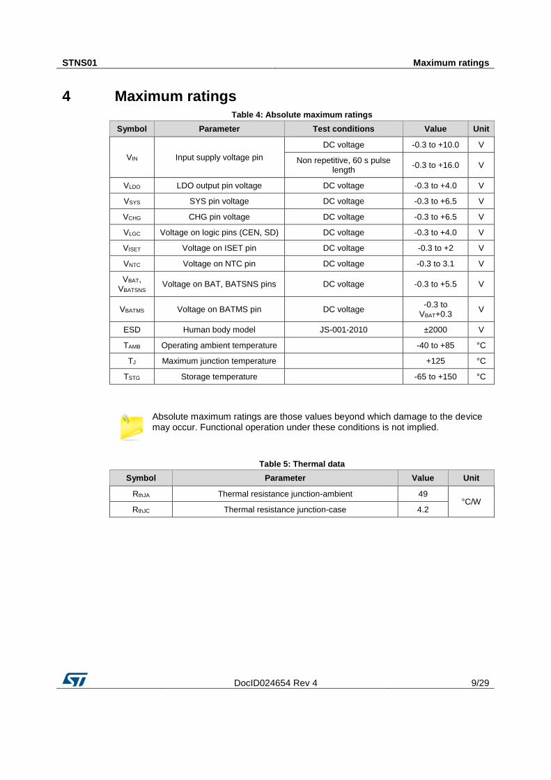
4 Maximum ratings Table 4: Absolute maximum ratings
Symbol Parameter Test conditions Value Unit
VIN Input supply voltage pin
DC voltage -0.3 to +10.0 V
Non repetitive, 60 s pulse length
-0.3 to +16.0 V
VLDO LDO output pin voltage DC voltage -0.3 to +4.0 V
VSYS SYS pin voltage DC voltage -0.3 to +6.5 V
VCHG CHG pin voltage DC voltage -0.3 to +6.5 V
VLGC Voltage on logic pins (CEN, SD) DC voltage -0.3 to +4.0 V
VISET Voltage on ISET pin DC voltage -0.3 to +2 V
VNTC Voltage on NTC pin DC voltage -0.3 to 3.1 V
VBAT, VBATSNS
Voltage on BAT, BATSNS pins DC voltage -0.3 to +5.5 V
VBATMS Voltage on BATMS pin DC voltage -0.3 to
VBAT+0.3 V
ESD Human body model JS-001-2010 ±2000 V
TAMB Operating ambient temperature
-40 to +85 °C
TJ Maximum junction temperature
+125 °C
TSTG Storage temperature
-65 to +150 °C
Absolute maximum ratings are those values beyond which damage to the device may occur. Functional operation under these conditions is not implied.
Table 5: Thermal data
Symbol Parameter Value Unit
RthJA Thermal resistance junction-ambient 49 °C/W
RthJC Thermal resistance junction-case 4.2
Electrical characteristics STNS01
10/29 DocID024654 Rev 4
5 Electrical characteristics
The values given in the following table are valid for - 40 °C < TJ < + 85 °C, VIN = 5 V, VBAT = 3.6 V, CLDO = 1 µF, CBAT = 4.7 µF, CIN = CSYS = 2.2 µF, RISET = 1 kΩ, SD = low, CEN = high, unless otherwise specified.
Table 6: Electrical characteristics
Symbol Parameter Test conditions Min. Typ. Max. Unit
VIN Operating input voltage VIN rising 4.55
5.4 V
VINOVP Input overvoltage protection VIN rising 5.6 5.9 6.2 V
VINOVPH Input overvoltage protection
hysteresis VIN falling
200
mV
VUVLO Undervoltage lock-out VIN falling 3.95 4.18 4.35 V
VUVLOH Undervoltage lock-out
hysteresis VIN rising
300
mV
IIN IN supply current
Charger disabled mode (CEN = low), ISYS = ILDO = 0 A
400
μA
Charging, VHOT < VNTC < VCOLD, including RISET current
1.4
mA
VFLOAT Battery floating voltage IBAT = 1 mA 4.158 4.2 4.242 V
IBAT BAT pin supply current
Battery-powered mode (VIN < VUVLO), ILDO = 0 A
6 10 µA
Standby mode, charge terminated
6 10 µA
Shutdown mode (SD = high)
100 500
nA Over-discharge mode (VBAT < VODC, VIN < VUVLO)
100 500
IFAST Fast-charge current
RISET = 500 Ω, constant-current mode ILDO + ISYS < 100 mA
400
mA RISET = 1 kΩ, constant-current
mode 180 200 220
RISET = 13 kΩ, constant-current mode
12 15 18
RISET Fast-charge programming
resistor range 1
13 kΩ
VISET ISET regulated voltage
1
VPRE Pre-charge to fast-charge battery voltage threshold
Charger active
3
V
IPRE Pre-charge current VBAT < 3 V, charger active
20
%IFAST
IEND End-of-charge current Charging in CV mode
10
%IFAST
VOCHG Battery voltage overcharge
threshold VBAT rising 4.245 4.275 4.305 V
VODC Battery voltage over-discharge threshold
VIN < VUVLO, ILDO = 100 mA 2.750 2.8 2.850 V
VODCR Battery voltage over-
discharge release threshold 3.0
V
STNS01 Electrical characteristics
DocID024654 Rev 4 11/29
Symbol Parameter Test conditions Min. Typ. Max. Unit
RON-IB Input to battery on-resistance
1 1.5 Ω
RON-BS Battery to SYS on-resistance ISINK = 100 mA
0.38 0.55 Ω
RON-
BATMS BATSNS to BATMS on-
resistance ISINK = 500 µA
270
Ω
VOL Output low level (CHG) ISINK = 5 mA
0.4 V
VIL Logic low input level (CEN,
SD) VLDO = 3.1 V
0.4 V
VIH Logic high input level (CEN,
SD) 1.6
V
RUP CEN pull-up resistor
375 500 625 kΩ
RDOWN SD pull-down resistor
375 500 625 kΩ
VLDO LDO output voltage ILDO = 1 mA 3.007 3.1 3.193 V
ΔVOUT-
LOAD LDO static load regulation ILDO = 1 mA to 150 mA
±0.002
%/mA
ISC LDO short-circuit current RLOAD = 0 Ω 250 350
mA
IBATOCP Battery discharge overcurrent
protection VIN<VUVLO (powered from BAT) 400
650 mA
IINLIM Input current limitation VSYS> VILIMSCTH; VUVLO < VIN <
VINOVP (powered from IN) 1
A
IINIMSCTH Input current limitation in short-circuit conditions
VSYS < VILIMSCTHINOVP (powered from IN)
400
mA
VILIMSCT H SYS voltage threshold for
input current limitation short-circuit detection
VUVLO < VIN < VINOVP
2
V
VSCLDO LDO short-circuit protection
threshold VIN < VUVLO or VIN > VINOVP
(powered from BAT) 0.7
V
VSCSYS SYS short-circuit protection
threshold VIN < VUVLO or VIN > VINOVP
(powered from BAT) VBAT -
0.8 V
INTCB NTC pin bias current VNTC = 0.25 V 48 50 52 µA
VHOT Thermal hot threshold Increasing NTC temperature 0.234 0.246 0.258 V
VCOLD Thermal cold threshold Decreasing NTC temperature 1.28 1.355 1.43 V
THYST Hot/cold temperature threshold hysteresis
10 kΩ NTC, ß = 3370
3
°C
TSD Thermal shutdown die
temperature 180
°C
TFAULT CHG pin blinking frequency Fault condition
1
Hz
tCHGD Input voltage connection to
charging-start delay
VBAT = 3.5 V, RNTC = 10 kΩ, battery detection not included
(tBDSRC + tBDSNK)
240
ms
tOCD Overcharge detection delay VBAT> VOCHG, VUVLO<VIN<VINOVP
1.2
s
tODD Over-discharge detection
delay VBAT < VODC and VIN < VUVLO or
VIN> VINOVP 400
ms
Electrical characteristics STNS01
12/29 DocID024654 Rev 4
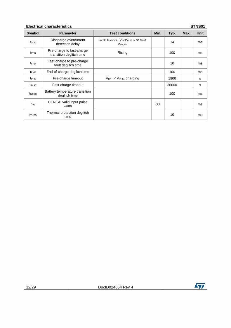
Symbol Parameter Test conditions Min. Typ. Max. Unit
tDOD Discharge overcurrent
detection delay IBAT> IBATOCP, VIN<VUVLO or VIN>
VINOVP 14
ms
tPFD Pre-charge to fast-charge
transition deglitch time Rising
100
ms
tFPD Fast-charge to pre-charge
fault deglitch time 10
ms
tEND End-of-charge deglitch time
100
ms
tPRE Pre-charge timeout VBAT < VPRE, charging
1800
s
tFAST Fast-charge timeout
36000
s
tNTCD Battery temperature transition
deglitch time 100
ms
tPW CEN/SD valid input pulse
width 30
ms
tTHPD Thermal protection deglitch
time 10
ms
STNS01 Typical performance characteristics (curves)
DocID024654 Rev 4 13/29
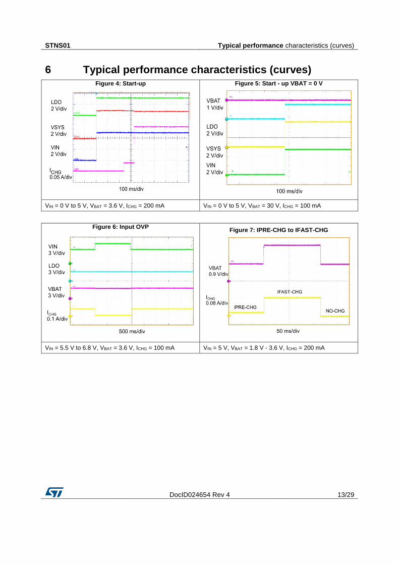
6 Typical performance characteristics (curves) Figure 4: Start-up
Figure 5: Start - up VBAT = 0 V
VIN = 0 V to 5 V, VBAT = 3.6 V, ICHG = 200 mA VIN = 0 V to 5 V, VBAT = 30 V, ICHG = 100 mA
Figure 6: Input OVP
Figure 7: IPRE-CHG to IFAST-CHG
VIN = 5.5 V to 6.8 V, VBAT = 3.6 V, ICHG = 100 mA VIN = 5 V, VBAT = 1.8 V - 3.6 V, ICHG = 200 mA
Typical performance characteristics (curves) STNS01
14/29 DocID024654 Rev 4
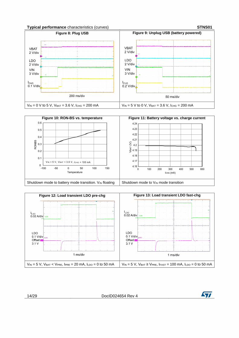
Figure 8: Plug USB
Figure 9: Unplug USB (battery powered)
VIN = 0 V to 5 V, VBAT = 3.6 V, ICHG = 200 mA VIN = 5 V to 0 V, VBAT = 3.6 V, ICHG = 200 mA
Figure 10: RON-BS vs. temperature
Figure 11: Battery voltage vs. charge current
Shutdown mode to battery mode transition. VIN floating Shutdown mode to VIN mode transition
Figure 12: Load transient LDO pre-chg
Figure 13: Load transient LDO fast-chg
VIN = 5 V, VBAT < VPRE, IPRE = 20 mA, ILDO = 0 to 50 mA VIN = 5 V, VBAT ≥ VPRE, IFAST = 100 mA, ILDO = 0 to 50 mA
STNS01 Typical performance characteristics (curves)
DocID024654 Rev 4 15/29
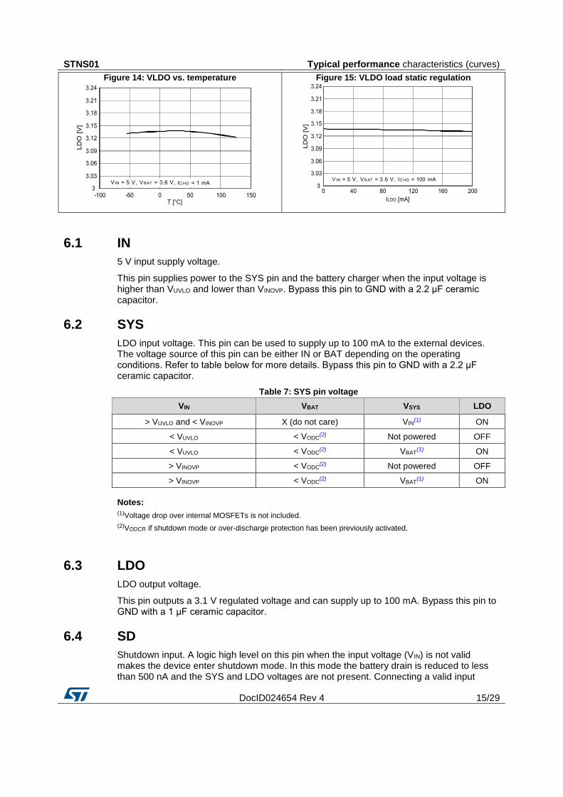
Figure 14: VLDO vs. temperature
Figure 15: VLDO load static regulation
6.1 IN
5 V input supply voltage.
This pin supplies power to the SYS pin and the battery charger when the input voltage is higher than VUVLO and lower than VINOVP. Bypass this pin to GND with a 2.2 μF ceramic capacitor.
6.2 SYS
LDO input voltage. This pin can be used to supply up to 100 mA to the external devices. The voltage source of this pin can be either IN or BAT depending on the operating conditions. Refer to table below for more details. Bypass this pin to GND with a 2.2 μF ceramic capacitor.
Table 7: SYS pin voltage
VIN VBAT VSYS LDO
> VUVLO and < VINOVP X (do not care) VIN(1) ON
< VUVLO < VODC(2) Not powered OFF
< VUVLO < VODC(2) VBAT
(1) ON
> VINOVP < VODC(2) Not powered OFF
> VINOVP < VODC(2) VBAT
(1) ON
Notes:
(1)Voltage drop over internal MOSFETs is not included. (2)VODCR if shutdown mode or over-discharge protection has been previously activated.
6.3 LDO
LDO output voltage.
This pin outputs a 3.1 V regulated voltage and can supply up to 100 mA. Bypass this pin to GND with a 1 μF ceramic capacitor.
6.4 SD
Shutdown input. A logic high level on this pin when the input voltage (VIN) is not valid makes the device enter shutdown mode. In this mode the battery drain is reduced to less than 500 nA and the SYS and LDO voltages are not present. Connecting a valid input
Typical performance characteristics (curves) STNS01
16/29 DocID024654 Rev 4
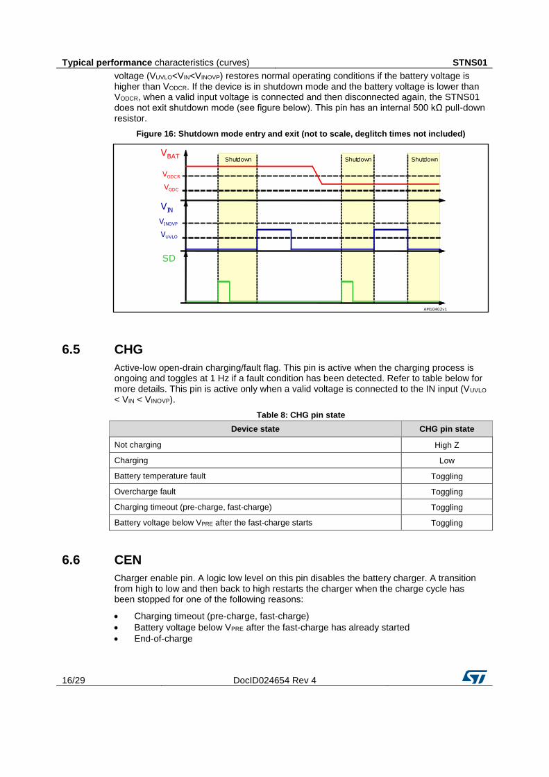
voltage (VUVLO<VIN<VINOVP) restores normal operating conditions if the battery voltage is higher than VODCR. If the device is in shutdown mode and the battery voltage is lower than VODCR, when a valid input voltage is connected and then disconnected again, the STNS01 does not exit shutdown mode (see figure below). This pin has an internal 500 kΩ pull-down resistor.
Figure 16: Shutdown mode entry and exit (not to scale, deglitch times not included)
6.5 CHG
Active-low open-drain charging/fault flag. This pin is active when the charging process is ongoing and toggles at 1 Hz if a fault condition has been detected. Refer to table below for more details. This pin is active only when a valid voltage is connected to the IN input (VUVLO < VIN < VINOVP).
Table 8: CHG pin state
Device state CHG pin state
Not charging High Z
Charging Low
Battery temperature fault Toggling
Overcharge fault Toggling
Charging timeout (pre-charge, fast-charge) Toggling
Battery voltage below VPRE after the fast-charge starts Toggling
6.6 CEN
Charger enable pin. A logic low level on this pin disables the battery charger. A transition from high to low and then back to high restarts the charger when the charge cycle has been stopped for one of the following reasons:
Charging timeout (pre-charge, fast-charge)
Battery voltage below VPRE after the fast-charge has already started
End-of-charge
STNS01 Typical performance characteristics (curves)
DocID024654 Rev 4 17/29
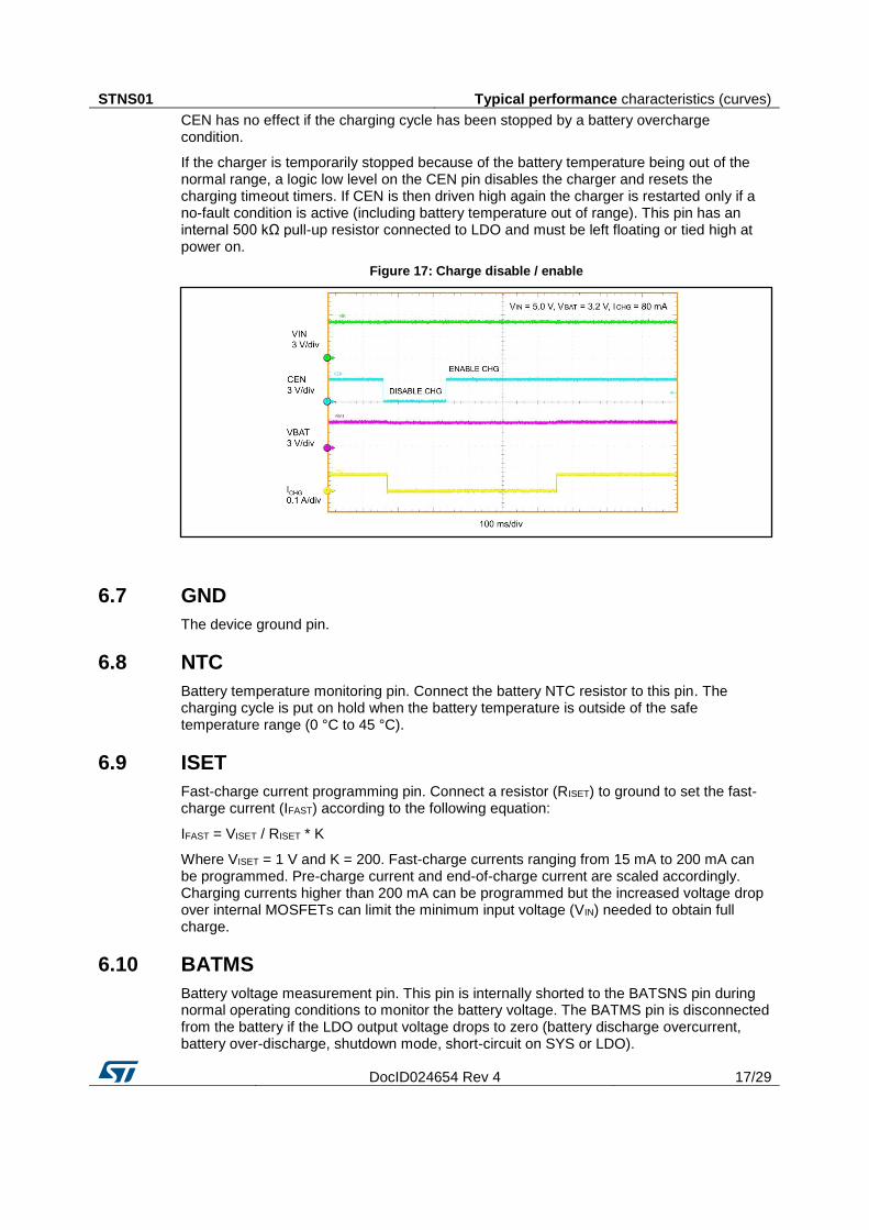
CEN has no effect if the charging cycle has been stopped by a battery overcharge condition.
If the charger is temporarily stopped because of the battery temperature being out of the normal range, a logic low level on the CEN pin disables the charger and resets the charging timeout timers. If CEN is then driven high again the charger is restarted only if a no-fault condition is active (including battery temperature out of range). This pin has an internal 500 kΩ pull-up resistor connected to LDO and must be left floating or tied high at power on.
Figure 17: Charge disable / enable
6.7 GND
The device ground pin.
6.8 NTC
Battery temperature monitoring pin. Connect the battery NTC resistor to this pin. The charging cycle is put on hold when the battery temperature is outside of the safe temperature range (0 °C to 45 °C).
6.9 ISET
Fast-charge current programming pin. Connect a resistor (RISET) to ground to set the fast-charge current (IFAST) according to the following equation:
IFAST = VISET / RISET * K
Where VISET = 1 V and K = 200. Fast-charge currents ranging from 15 mA to 200 mA can be programmed. Pre-charge current and end-of-charge current are scaled accordingly. Charging currents higher than 200 mA can be programmed but the increased voltage drop over internal MOSFETs can limit the minimum input voltage (VIN) needed to obtain full charge.
6.10 BATMS
Battery voltage measurement pin. This pin is internally shorted to the BATSNS pin during normal operating conditions to monitor the battery voltage. The BATMS pin is disconnected from the battery if the LDO output voltage drops to zero (battery discharge overcurrent, battery over-discharge, shutdown mode, short-circuit on SYS or LDO).
Typical performance characteristics (curves) STNS01
18/29 DocID024654 Rev 4
6.11 BATSNS
Battery voltage sense pin. This pin is needed to ensure accuracy on the floating voltage and battery voltage protection thresholds. The BATSNS pin must be connected as close as possible to the battery positive terminal.
6.12 BAT
Battery positive terminal connection pin. Bypass this pin to GND with a 4.7 μF ceramic capacitor.
STNS01 Operation description
DocID024654 Rev 4 19/29
7 Operation description
The STNS01 is a power management IC integrating a battery charger with a power path function, a battery temperature monitoring and a 3.1 V 100 mA LDO.
When a valid input voltage (VIN) is present on the IN pin, after security checks are performed, the battery charger starts charging the battery using a constant-current/constant-voltage charging algorithm. The input voltage (VIN) is considered to be valid if it is higher than VUVLO and lower than VINOVP. The power path architecture allows charging the battery and supplying the system at the same time. When the input voltage is not valid, the LDO (and every external IC connected to SYS) is supplied by the battery through a low resistance path. The device also provides protection to the battery against the following fault conditions:
Overcharge
Over-discharge
Charge overcurrent
Discharge overcurrent
If a fault condition is detected when the input voltage is valid (VUVLO < VIN < VINOVP), the CHG pin starts toggling, to inform the control logic that an error occurred.
The device can also be put in reduced battery drain mode (shutdown, IBAT < 500 nA) to maximize battery life during end-product shipping and shelf time.
7.1 Power-on
When the device is in shutdown mode, the pins LDO and SYS are not supplied. In order to turn the device on a valid input voltage must be connected (VIN). The CEN pin must be floating or tied high during power-on for proper operations.
7.2 Battery charger
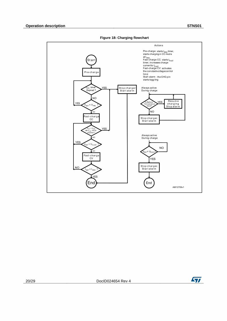
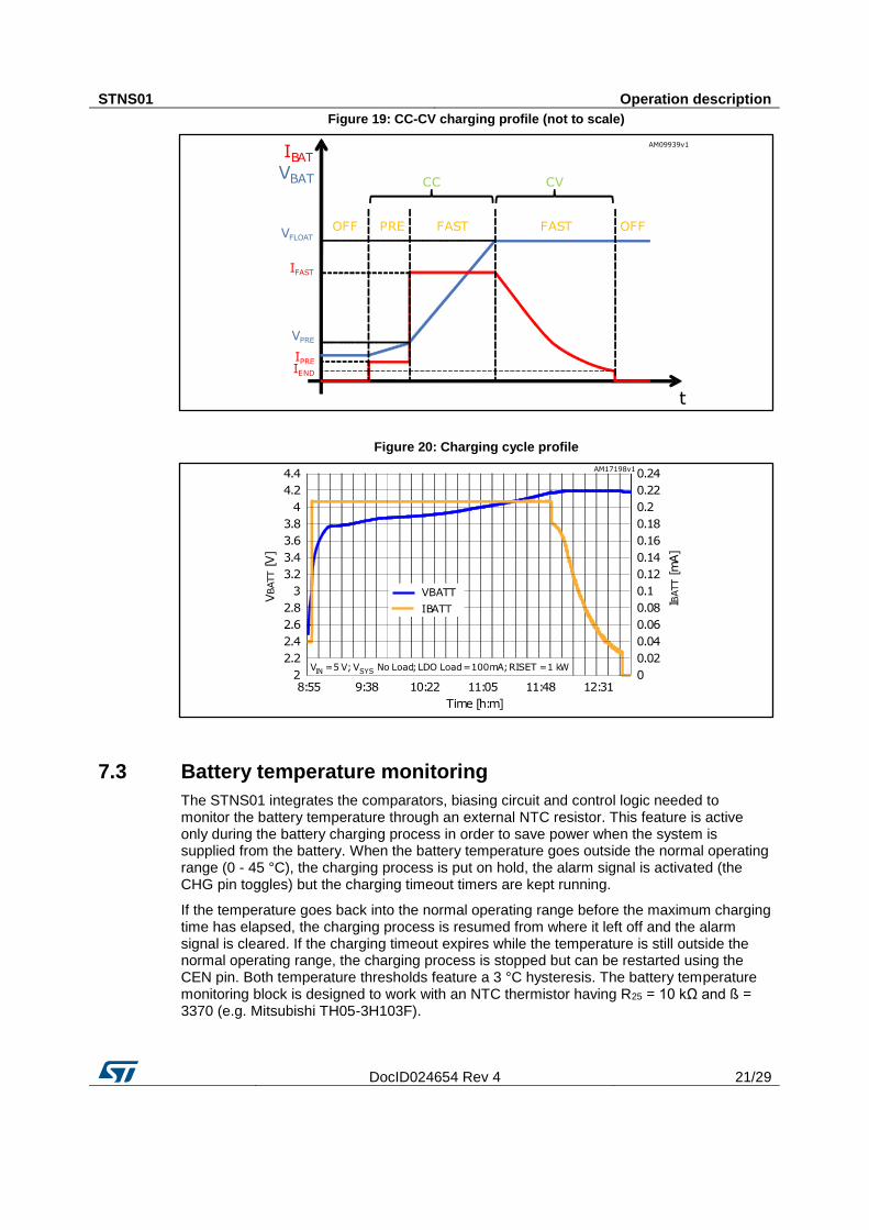
The STNS01's battery charger is designed to charge single cell Li-Ion batteries up to 4.2 V using a CC-CV charging algorithm. When a valid input voltage is detected, the STNS01 starts the charge cycle and the CHG pin switches from high impedance to low level. The charging process starts if the battery voltage is higher than VBATMIN. If the battery is deeply discharged (the battery voltage is lower than VPRE and higher than VBATMIN) the charger enters the pre-charge phase and starts charging in constant-current mode using a low current (IPRE = 20% IFAST). If the battery voltage does not reach the VPRE threshold within tPRE, the charging process is stopped and a fault is signaled. When the battery voltage reaches the VPRE threshold, the constant-current fast-charge phase is entered and the charging current is increased to IFAST. The value of IFAST can be programmed from 15 mA to 200 mA using an external resistor as described in the ISET pin description. Once the fast-charge phase has started, if the battery voltage decreases again below VPRE, the charging process is stopped and a fault is signaled. The constant-current fast-charge phase lasts as long as the battery voltage is lower than VFLOAT. When VBAT reaches VFLOAT, the charging algorithm switches to constant-voltage (CV) mode. During the CV mode the battery voltage is regulated to VFLOAT and the charging current starts decreasing. When the charging current reaches the IEND threshold (IEND = 10% IFAST), the charging process is stopped and the CHG pin is put in high impedance. If the fast-charge phase is not terminated within tFAST, the charging process is stopped and a fault is signaled. The battery temperature is monitored throughout the charging cycle for safety reasons. Refer to figure below for a simplified flowchart of the charging process.
Operation description STNS01
20/29 DocID024654 Rev 4
Figure 18: Charging flowchart
STNS01 Operation description
DocID024654 Rev 4 21/29
Figure 19: CC-CV charging profile (not to scale)
Figure 20: Charging cycle profile
7.3 Battery temperature monitoring
The STNS01 integrates the comparators, biasing circuit and control logic needed to monitor the battery temperature through an external NTC resistor. This feature is active only during the battery charging process in order to save power when the system is supplied from the battery. When the battery temperature goes outside the normal operating range (0 - 45 °C), the charging process is put on hold, the alarm signal is activated (the CHG pin toggles) but the charging timeout timers are kept running.
If the temperature goes back into the normal operating range before the maximum charging time has elapsed, the charging process is resumed from where it left off and the alarm signal is cleared. If the charging timeout expires while the temperature is still outside the normal operating range, the charging process is stopped but can be restarted using the CEN pin. Both temperature thresholds feature a 3 °C hysteresis. The battery temperature monitoring block is designed to work with an NTC thermistor having R25 = 10 kΩ and ß = 3370 (e.g. Mitsubishi TH05-3H103F).
Operation description STNS01
22/29 DocID024654 Rev 4
7.4 Battery overcharge protection
The battery overcharge protection is a safety feature, active when a valid input voltage is connected, preventing the battery voltage from exceeding a VOCHG value. Should an overcharge condition be detected, the current path from the input to the battery is blocked and a fault signal is activated (the CHG pin toggles at 8.2 Hz). When the battery voltage goes below VOCHG, normal operations can only be restarted by disconnecting and connecting back again the input voltage (VIN).
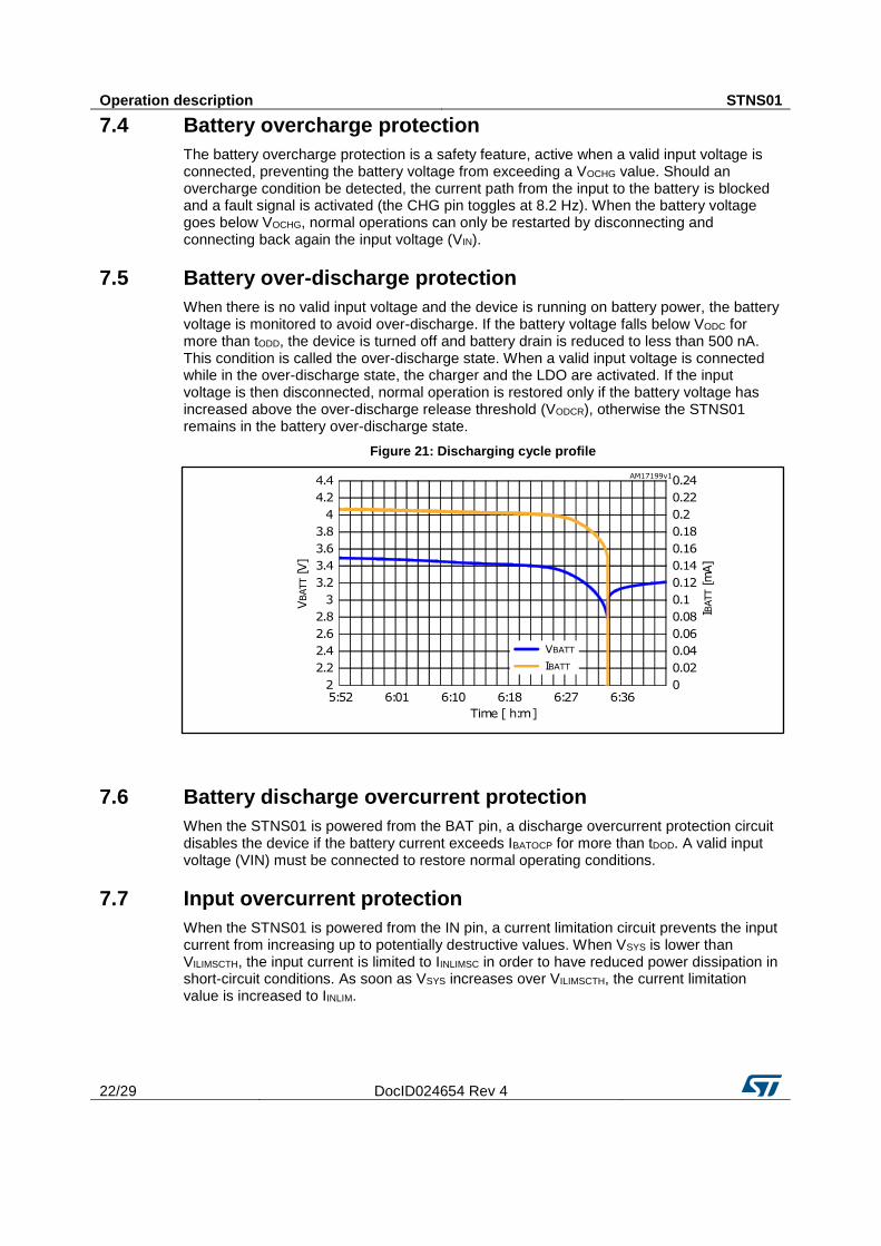
7.5 Battery over-discharge protection
When there is no valid input voltage and the device is running on battery power, the battery voltage is monitored to avoid over-discharge. If the battery voltage falls below VODC for more than tODD, the device is turned off and battery drain is reduced to less than 500 nA. This condition is called the over-discharge state. When a valid input voltage is connected while in the over-discharge state, the charger and the LDO are activated. If the input voltage is then disconnected, normal operation is restored only if the battery voltage has increased above the over-discharge release threshold (VODCR), otherwise the STNS01 remains in the battery over-discharge state.
Figure 21: Discharging cycle profile
7.6 Battery discharge overcurrent protection
When the STNS01 is powered from the BAT pin, a discharge overcurrent protection circuit disables the device if the battery current exceeds IBATOCP for more than tDOD. A valid input voltage (VIN) must be connected to restore normal operating conditions.
7.7 Input overcurrent protection
When the STNS01 is powered from the IN pin, a current limitation circuit prevents the input current from increasing up to potentially destructive values. When VSYS is lower than VILIMSCTH, the input current is limited to IINLIMSC in order to have reduced power dissipation in short-circuit conditions. As soon as VSYS increases over VILIMSCTH, the current limitation value is increased to IINLIM.
STNS01 Operation description
DocID024654 Rev 4 23/29
7.8 SYS and LDO short-circuit protection
In case of an abrupt short-circuit on SYS or LDO, the STNS01 is immediately turned off (no deglitch). This short-circuit protection intervenes when the SYS voltage drops below VSCSYS or the LDO output voltage drops below VSCLDO.
7.9 IN overvoltage protection
The STNS01 is normally powered from the battery when VIN > VINOVP while it is powered from the IN pin when VUVLO < VIN < VINOVP. In the latter case, if the input voltage temporarily increases over VINOVP due to a poorly regulated power supply, the STNS01 switches to battery power to protect any external circuit connected to SYS. If the input voltage (VIN) returns into the normal range, the device's supply voltage is switched back to the IN pin.
7.10 Shutdown mode
A high level on the shutdown digital input pin (SD) when no valid input voltage is connected makes the device enter shutdown (low power) mode. Battery drain is then reduced to less than 500 nA. The exit conditions for the shutdown mode are the same as for the over-discharge state (valid VIN connected and VBAT > VODCR).
7.11 Thermal shutdown
The STNS01 is protected against overheating which might be generated by the combination of ambient temperature and internal heating due to power dissipation. When the die temperature exceeds TSD the device is turned off. In order to restore normal operation the input voltage (VIN) must be disconnected and reconnected.
7.12 Reverse current protection
In order to prevent undesired battery discharge, when the input voltage (VIN) is lower than the battery voltage (VBAT), the current path from BAT to IN is blocked.
Package information STNS01
24/29 DocID024654 Rev 4
8 Package information
In order to meet environmental requirements, ST offers these devices in different grades of ECOPACK® packages, depending on their level of environmental compliance. ECOPACK® specifications, grade definitions and product status are available at: www.st.com. ECOPACK® is an ST trademark.
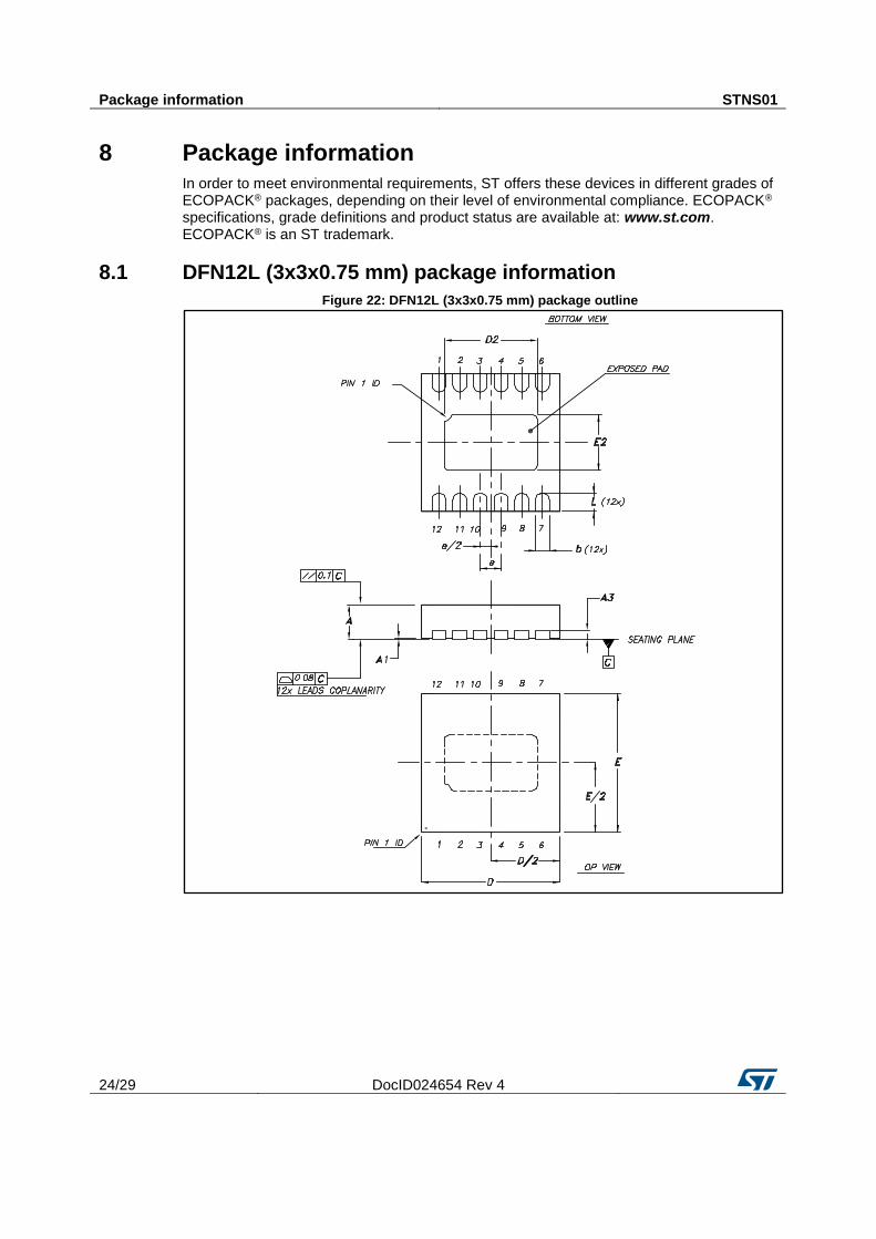
8.1 DFN12L (3x3x0.75 mm) package information
Figure 22: DFN12L (3x3x0.75 mm) package outline
STNS01 Package information
DocID024654 Rev 4 25/29
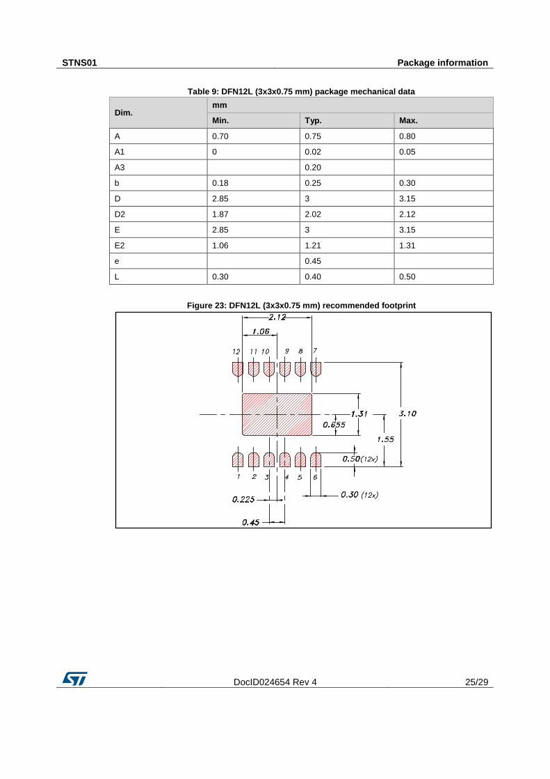
Table 9: DFN12L (3x3x0.75 mm) package mechanical data
Dim. mm
Min. Typ. Max.
A 0.70 0.75 0.80
A1 0 0.02 0.05
A3
0.20
b 0.18 0.25 0.30
D 2.85 3 3.15
D2 1.87 2.02 2.12
E 2.85 3 3.15
E2 1.06 1.21 1.31
e
0.45
L 0.30 0.40 0.50
Figure 23: DFN12L (3x3x0.75 mm) recommended footprint
Package information STNS01
26/29 DocID024654 Rev 4
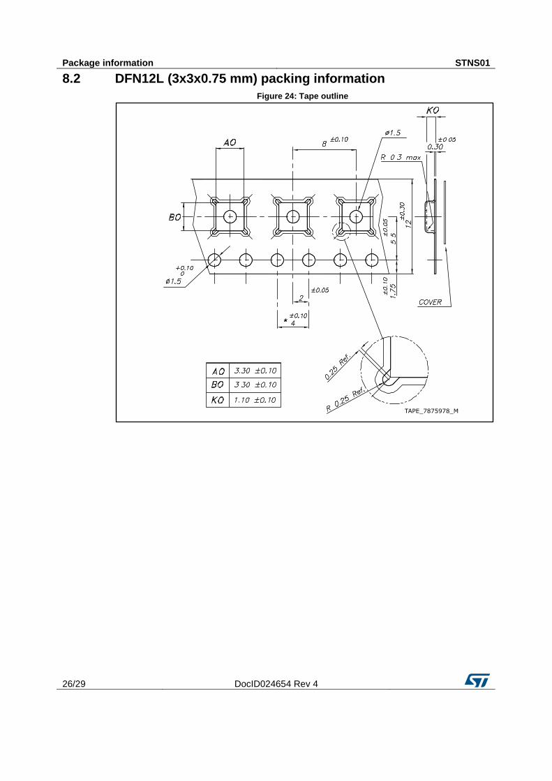
8.2 DFN12L (3x3x0.75 mm) packing information
Figure 24: Tape outline
STNS01 Package information
DocID024654 Rev 4 27/29
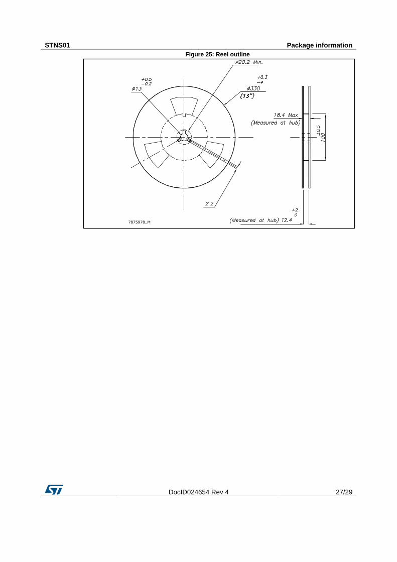
Figure 25: Reel outline
Revision history STNS01
28/29 DocID024654 Rev 4
9 Revision history Table 10: Document revision history
Date Revision Changes
17-May-2013 1 Initial release.
15-Jul-2013 2 Updated Table 6: Electrical characteristics.
11-May-2017 3 Updated section 5: "Electrical characteristics".
14-Dec-2017 4 Updated Table 5: "Thermal data" and Table 6:
"Electrical characteristics".
STNS01
DocID024654 Rev 4 29/29
IMPORTANT NOTICE – PLEASE READ CAREFULLY
STMicroelectronics NV and its subsidiaries (“ST”) reserve the right to make changes, corrections, enhancements, modifications, and improvements to ST products and/or to this document at any time without notice. Purchasers should obtain the latest relevant information on ST products before placing orders. ST products are sold pursuant to ST’s terms and conditions of sale in place at the time of order acknowledgement.
Purchasers are solely responsible for the choice, selection, and use of ST products and ST assumes no liability for application assistance or the design of Purchasers’ products.
No license, express or implied, to any intellectual property right is granted by ST herein.
Resale of ST products with provisions different from the information set forth herein shall void any warranty granted by ST for such product.
ST and the ST logo are trademarks of ST. All other product or service names are the property of their respective owners.
Information in this document supersedes and replaces information previously supplied in any prior versions of this document.
© 2017 STMicroelectronics – All rights reserved