lesson 20: preparing the schematic for the orcad and allegro pcb...
TRANSCRIPT

Getting Started with OrCAD Capture OrCAD Capture Version16.6
EMA Design Automation 385
Lesson 20: Preparing the Schematic for
the OrCAD and Allegro PCB
Editor
(Use this section to setup the design for the above tools.)
Lesson Objectives
After completing this lesson, you will be able to:
Add an OrCAD and Allegro PCB Editor part or net property to your design
Create a netlist for the OrCAD and Allegro PCB Editor
Part Properties for OrCAD and Allegro PCB Editor
There many OrCAD and Allegro PCB Editor part properties you can add to your design.
These are some of these properties are listed and described in the table that follows.
OrCAD and Allegro PCB
Editor Part Properties
Description
* PCB Footprint Defines the OrCAD and Allegro PCB Editor
footprint pattern. All OrCAD and Allegro
PCB Editor parts are required to have this
property. The name of this property can be
up to 255 characters long and may include
the characters A-Z, 0-9, as well as the dash
(hyphen) and underscore characters. Blank
spaces within the name are not permitted.
ALT_SYMBOLS Lists of alternate footprint patterns you can
use apply to your part during PCB layout.
Each alternate footprint must have the
same pin count.
Getting Started with OrCAD Capture OrCAD Capture Version16.6
EMA Design Automation 386
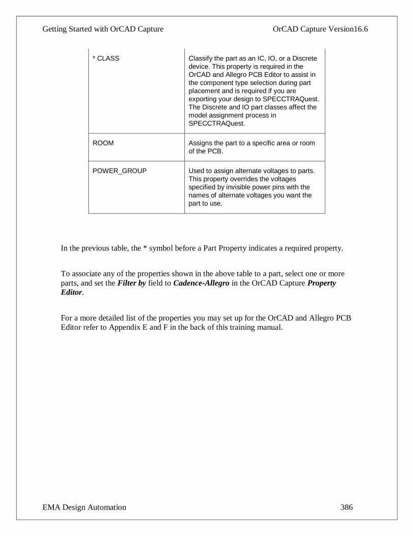
* CLASS Classify the part as an IC, IO, or a Discrete
device. This property is required in the
OrCAD and Allegro PCB Editor to assist in
the component type selection during part
placement and is required if you are
exporting your design to SPECCTRAQuest.
The Discrete and IO part classes affect the
model assignment process in
SPECCTRAQuest.
ROOM Assigns the part to a specific area or room
of the PCB.
POWER_GROUP Used to assign alternate voltages to parts.
This property overrides the voltages
specified by invisible power pins with the
names of alternate voltages you want the
part to use.
In the previous table, the * symbol before a Part Property indicates a required property.
To associate any of the properties shown in the above table to a part, select one or more
parts, and set the Filter by field to Cadence-Allegro in the OrCAD Capture Property
Editor.
For a more detailed list of the properties you may set up for the OrCAD and Allegro PCB
Editor refer to Appendix E and F in the back of this training manual.

Getting Started with OrCAD Capture OrCAD Capture Version16.6
EMA Design Automation 387
Grouping Parts for PCB Design
The above graphic illustrates how the ROOM property can be used to define the value
CHAN1 to all parts in the DAAMP1 schematic. This graphic shows how a polygon
defined on the OrCAD and Allegro PCB Editor board as CHAN1 can be used in the
OrCAD and Allegro PCB Editor to automatically place the DAAMP1 parts into the
CHAN1 room. If desired, the OrCAD and Allegro PCB Editor can be set up to display
error markers when parts are incorrectly located in a room.
Net Properties for the ORCAD and Allegro PCB Editor
There are many different ORCAD and Allegro PCB Editor net properties you can add to
your design. The table that follows describes five commonly used OrCAD Capture to
OrCAD and Allegro PCB Editor net properties. Refer to Appendix F for a more complete
list of additional net properties.
.
Getting Started with OrCAD Capture OrCAD Capture Version16.6
EMA Design Automation 388
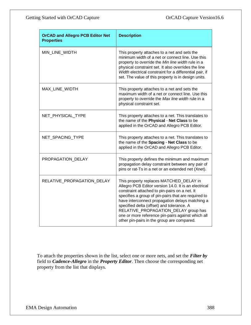
OrCAD and Allegro PCB Editor Net
Properties
Description
MIN_LINE_WIDTH This property attaches to a net and sets the
minimum width of a net or connect line. Use this property to override the Min line width rule in a
physical constraint set. It also overrides the line Width electrical constraint for a differential pair, if
set. The value of this property is in design units.
MAX_LINE_WIDTH This property attaches to a net and sets the
maximum width of a net or connect line. Use this property to override the Max line width rule in a
physical constraint set.
NET_PHYSICAL_TYPE This property attaches to a net. This translates to the name of the Physical - Net Class to be
applied in the OrCAD and Allegro PCB Editor.
NET_SPACING_TYPE This property attaches to a net. This translates to
the name of the Spacing - Net Class to be
applied in the OrCAD and Allegro PCB Editor.
PROPAGATION_DELAY This property defines the minimum and maximum
propagation delay constraint between any pair of
pins or rat-Ts in a net or an extended net (Xnet).
RELATIVE_PROPAGATION_DELAY This property replaces MATCHED_DELAY in
Allegro PCB Editor version 14.0. It is an electrical
constraint attached to pin-pairs on a net. It
specifies a group of pin-pairs that are required to
have interconnect propagation delays matching a
specified delta (offset) and tolerance. A
RELATIVE_PROPAGATION_DELAY group has
one or more reference pin-pairs against which all
other pin-pairs in the group are compared.
To attach the properties shown in the list, select one or more nets, and set the Filter by
field to Cadence-Allegro in the Property Editor. Then choose the corresponding net
property from the list that displays.

Getting Started with OrCAD Capture OrCAD Capture Version16.6
EMA Design Automation 389
Create Differential Pairs between flat nets
OrCAD Capture has the ability to allow you to create Differential Pairs between flat nets
in your design for the Allegro PCB Editor. You can set the DIFFERENTIAL_PAIR
property on selected nets using the Property Editor. See the Property filter for Cadence-
Allegro.
There is also a command Create Differential Pair located on the Tools pull-down menu.
In the Create Differential Pair dialog box you can view the nets defined in your design
and create a Differentials Pair between selected nets.
Getting Started with OrCAD Capture OrCAD Capture Version16.6
EMA Design Automation 390
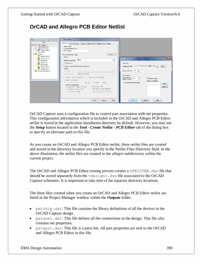
OrCAD and Allegro PCB Editor Netlist
OrCAD Capture uses a configuration file to control part association with net properties.
This configuration information which is included in the OrCAD and Allegro PCB Editor
netlist is stored in the application installation directory by default. However, you may use
the Setup button located in the Tool - Create Netlist - PCB Editor tab of the dialog box
to specify an alternate path to this file.
As you create an OrCAD and Allegro PCB Editor netlist, three netlist files are created
and stored in the directory location you specify in the Netlist Files Directory field. In the
above illustration, the netlist files are created in the allegro subdirectory within the
current project.
The OrCAD and Allegro PCB Editor routing process creates a SPECCTRA.dsn file that
should be stored separately from the <design>.dsn file associated to the OrCAD
Capture schematic. It is important to take note of the separate directory locations.
The three files created when you create an OrCAD and Allegro PCB Editor netlist are
listed in the Project Manager window within the Outputs folder.
pstchip.dat: This file contains the library definitions of all the devices in the
OrCAD Capture design.
pstxnet.dat: This file defines all the connections in the design. This file also
contains net properties.
pstxprt.dat: This file is a parts list. All part properties are sent to the OrCAD
and Allegro PCB Editor in this file.
Getting Started with OrCAD Capture OrCAD Capture Version16.6
EMA Design Automation 391
The Create Netlist window also lets you load the three netlist files into an OrCAD and
Allegro PCB Editor design.
You can use an alias in the configuration file to map an old Allegro PCB Editor property
into a new one. If you have a previous Allegro design that uses the DELAY_RULE
property, you can map this property to another property name (for example,
DELAY_RULE = PROPAGATION_DELAY).
Common Issues and Errors
The netlister has an Allegro PCB Editor-specific error checking mechanism that
generates a list of Allegro PCB Editor formatting errors, and halts the netlist generation.
The error messages are written to the session log. A netlist.log file is also written
to the current working directory.
The following table identifies and describes common problems associated with creating
or loading an OrCAD and Allegro PCB Editor netlist. For additional information, please
see Help - Product Notes within the OrCAD Capture application
Error Message Description
Missing PCB Footprint Every part in the design must have an assigned
PCB Footprint property to ensure operation of the
netlister. If you attempt to run the netlister before
PCB footprints are assigned, the process will
abort.
The footprint property can be defined through
either the library or parts in the design.

Getting Started with OrCAD Capture OrCAD Capture Version16.6
EMA Design Automation 392
No Connect Pins A pin with a No Connect symbol placed on it will
be tied to net name NC in the netlist. These are
unconnected pins, as opposed to No Connect
pins.
No Connect pins are non-electrical pins on the
physical package. No Connect pins are usually
not present on the OrCAD Capture symbol.
However, these pins must be defined, or else
errors occur when you load the netlist into the
OrCAD and Allegro PCB Editor. Use the NC
property to supply a list of No Connect pin
numbers for a part.
No connect pins can be added to the OrCAD
Capture symbol, but they must have unique pin
names (for example, NC1, NC2, and so on). Pins
that appear on the symbol should not be included
in any NC property.
OrCAD and Allegro PCB Editor package symbols
can contain mechanical pins, or pins without
numbers (for example, the mounting holes on a
connector). A part in the OrCAD Capture library
would not need an NC property to account for
these mounting holes.
Duplicate Pin Names If two or more visible pins have the same pin
name, the netlister will abort. However, if the pin
type is POWER, the netlister will automatically
alter the duplicated pin names to make them
unique.
Illegal Characters The netlist does not allow the use of single
quotes or exclamation marks in any pin, part, or
net names. It is best to use A-Z, 0-9, and the
underscore character as the only punctuation.
Missing Pin Number Every pin must have an assigned pin number.
The netlister will abort if you attempt to use it
before completing pin number assignments.
Creating an OrCAD and Allegro PCB Editor Netlist
You can create an OrCAD and Allegro PCB Editor netlist using the OrCAD Capture
commands Tools - Create Netlist - PCB Editor. Then import the three default OrCAD
and Allegro PCB Editor net files into OrCAD and Allegro PCB Editor.

Getting Started with OrCAD Capture OrCAD Capture Version16.6
EMA Design Automation 393
In your <install directory>, in the OrCAD Capture directory, is a configuration file that
lists the properties that the Netlister will extract from the OrCAD Capture Schematic for
both Parts and Nets. This file is the Allegro.cfg file. These are also the properties
that you will find listed under the Cadence-Allegro property filter in the OrCAD Capture
schematic editor. (See how to edit or create property filters in Lesson 13 of this manual.)
General Rules for Netlisting
The OrCAD and Allegro PCB Editor netlister extracts 3 ASCII files: PSTCHIP,
PSTXNET, and PSTXPRT.
Make sure that ALL parts have a PCB Footprint value.
Pin counts of the OrCAD Capture part must match the physical symbol (footprint).
ALL pins must have a pin name and number in the OrCAD Capture part.
To account for UNUSED pins (such as component mounting holes) use the NC part
property to list them or make the pins in the physical symbol (footprint) mechanical
pins.
There are attribute length limits and character limits for the OrCAD and Allegro PCB
Editor. See the following chart.
Getting Started with OrCAD Capture OrCAD Capture Version16.6
EMA Design Automation 394
* In the OrCAD and Allegro PCB Editor the default maximum number of characters is
30. You can set the initial length for new designs to a maximum length of 255 by using
the allegro_long_name_size environment variable (Choose Setup - User Preferences).
You can change the size in existing designs by choosing Set - design Parameters and
specifying a new maximum for the Long Name Size in the Design Tab.
Remember, it is recommended that you avoid the use of spaces in directory names,
design names and net names.
Common Errors
View these error messages in the OrCAD Capture Session Log.
PCB Footprint missing in OrCAD Capture
Footprint does not match library (symbol) name
Cannot find symbol - psm or pad path incorrect
Pin mismatch - pin numbers or total pin counts do not march from Footprint to
component symbol
Pin name not allowed
Pin Number missing in OrCAD Capture part.
Getting Started with OrCAD Capture OrCAD Capture Version16.6
EMA Design Automation 395
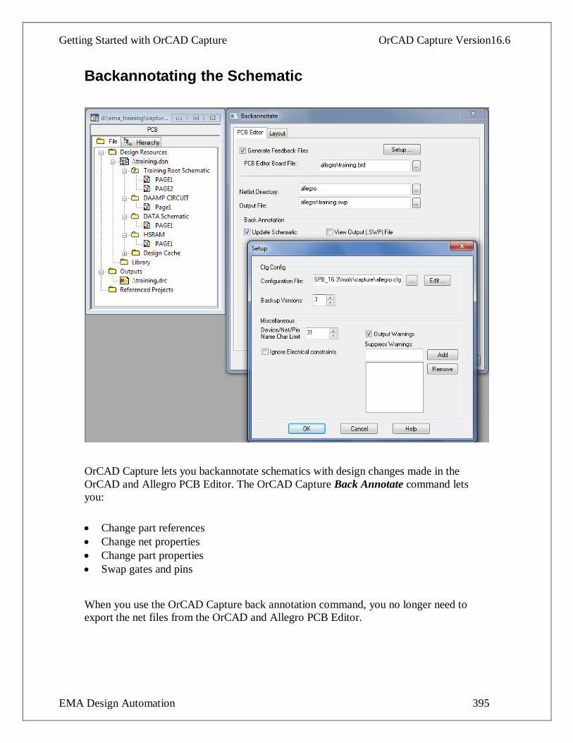
Backannotating the Schematic
OrCAD Capture lets you backannotate schematics with design changes made in the
OrCAD and Allegro PCB Editor. The OrCAD Capture Back Annotate command lets
you:
Change part references
Change net properties
Change part properties
Swap gates and pins
When you use the OrCAD Capture back annotation command, you no longer need to
export the net files from the OrCAD and Allegro PCB Editor.

Getting Started with OrCAD Capture OrCAD Capture Version16.6
EMA Design Automation 396
In the OrCAD and Allegro PCB Editor, when you use the File - Export Logic command
to send information back to the OrCAD Capture schematic, the OrCAD and Allegro PCB
Editor produces four backannotation files:
pinView.dat: Contains all pins and net connections
netView.dat: Contains all net properties
compView.dat: Contains all part properties
funcView.dat: Contains all gate properties
These files can also be produced in OrCAD Capture using the Tools - Back Annotate
command, and selecting the Generate Feedback Files option.
In OrCAD Capture, when you use the Tools - Back Annotate command, these four files
are processed into a single backannotation file, called a swap file. The swap file is then
used to update the OrCAD Capture schematic with new part references, as well as part
and net properties.
All gate and pin swapping data is automatically included in the swap file. The
backannotation of part and net properties is controlled by the Allegro.cfg file.
The Export - Logic files for the Back Annotation process must be in the same “Allegro”
subdirectory as the original Net List files.
Getting Started with OrCAD Capture OrCAD Capture Version16.6
EMA Design Automation 397
Lab 20-1: Adding OrCAD and Allegro PCB
Editor Properties
Lab Objectives
After completing this lab you will be able to:
Browse parts
Add a PCB Footprint property
Add other properties
View the Occurrence properties
An alternate method for doing some of the following labs is to use the Property Editor
and the Edit Object Properties method from the Project Manager window.
Browsing Parts
1. In the Training Project Manager window, click .\training.dsn, and select Edit -
Object Properties.
The Property Editor window opens displaying the current properties of all of the
parts in the design.
2. Set Filter by to: Cadence-Allegro.
3. Close the Property Editor window.
4. Select Edit - Browse - Parts from the main menu.
5. Click OK to continue.
The Browse Parts window lists all the parts in the design.
Adding the PCB Footprint Property
1. Scroll down and click on part reference U5.
2. Select Edit - Properties from the pop-up menu.
The Browse Spreadsheet displays properties currently attached to U5.
3. Locate the PCB Footprint column to verify a cell value of PLCC84.
4. If necessary, click in the cell, and enter: PLCC84
5. Click OK to continue.
6. Close the Browse Parts window, and save the design.
Getting Started with OrCAD Capture OrCAD Capture Version16.6
EMA Design Automation 398
Browsing Nets
1. In the Project Manager window, click on .\training.dsn, and select Edit -
Browse - Nets.
2. Click OK to continue.
The Browse Nets window lists all the nets in the design.
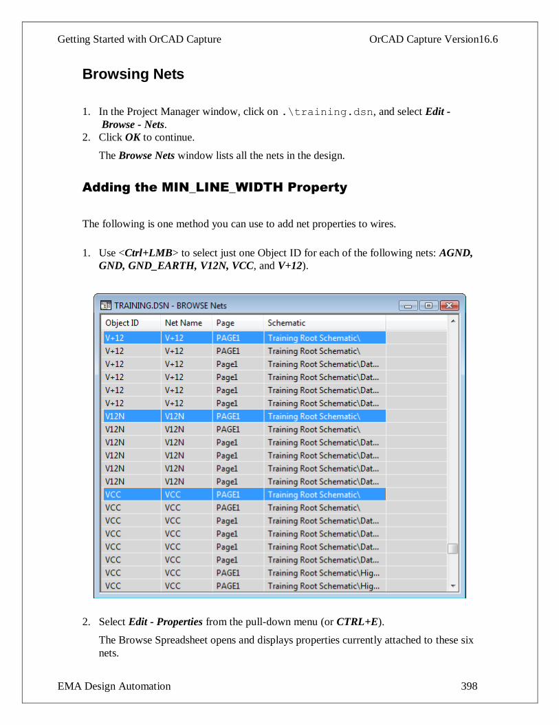
Adding the MIN_LINE_WIDTH Property
The following is one method you can use to add net properties to wires.
1. Use <Ctrl+LMB> to select just one Object ID for each of the following nets: AGND,
GND, GND_EARTH, V12N, VCC, and V+12).
2. Select Edit - Properties from the pull-down menu (or CTRL+E).
The Browse Spreadsheet opens and displays properties currently attached to these six
nets.
Getting Started with OrCAD Capture OrCAD Capture Version16.6
EMA Design Automation 399
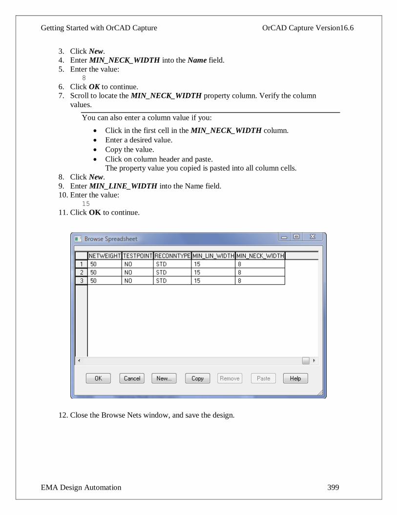
3. Click New.
4. Enter MIN_NECK_WIDTH into the Name field.
5. Enter the value: 8
6. Click OK to continue.
7. Scroll to locate the MIN_NECK_WIDTH property column. Verify the column
values.
You can also enter a column value if you:
Click in the first cell in the MIN_NECK_WIDTH column.
Enter a desired value.
Copy the value.
Click on column header and paste.
The property value you copied is pasted into all column cells.
8. Click New.
9. Enter MIN_LINE_WIDTH into the Name field.
10. Enter the value: 15
11. Click OK to continue.
12. Close the Browse Nets window, and save the design.

Getting Started with OrCAD Capture OrCAD Capture Version16.6
EMA Design Automation 400
Browsing Parts in the DAAMP Circuit
The following is only one of the ways to assign a property to parts in the OrCAD Capture
Schematic.
1. In the Project Manager window, click on the DAAMP Circuit schematic folder, and
select Edit - Browse - Parts.
2. Click OK to continue.
The Browse Parts window lists every occurrence of every part found in the DAAMP1
and DAAMP2 blocks.
Adding a ROOM Property to DAAMP1
1. Widen the column labeled Schematic to see the entire schematic path for each
occurrence.
2. Click on the Schematic column heading to sort the entries by schematic path.
All the DAAMP1 parts are now at the top of the list. The result is shown in the
following picture.
3. In the Reference column, use the <Shift> key and left mouse button (LMB) to group
select all the parts on the DAAMP1 page (as shown above).
4. Select Edit - Properties from the pull-down menu.
The Browse Spreadsheet appears, listing the selected part occurrences and their
current properties.
Getting Started with OrCAD Capture OrCAD Capture Version16.6
EMA Design Automation 401
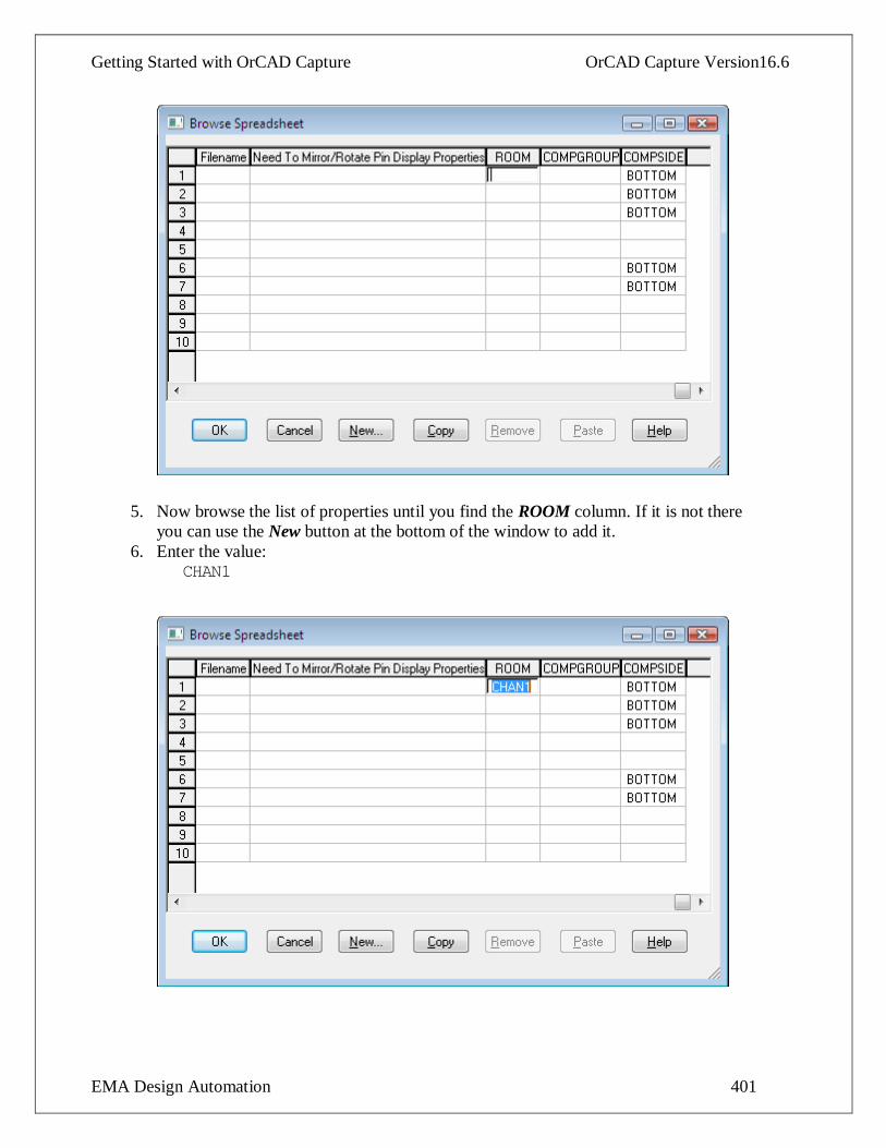
5. Now browse the list of properties until you find the ROOM column. If it is not there
you can use the New button at the bottom of the window to add it.
6. Enter the value: CHAN1
Getting Started with OrCAD Capture OrCAD Capture Version16.6
EMA Design Automation 402
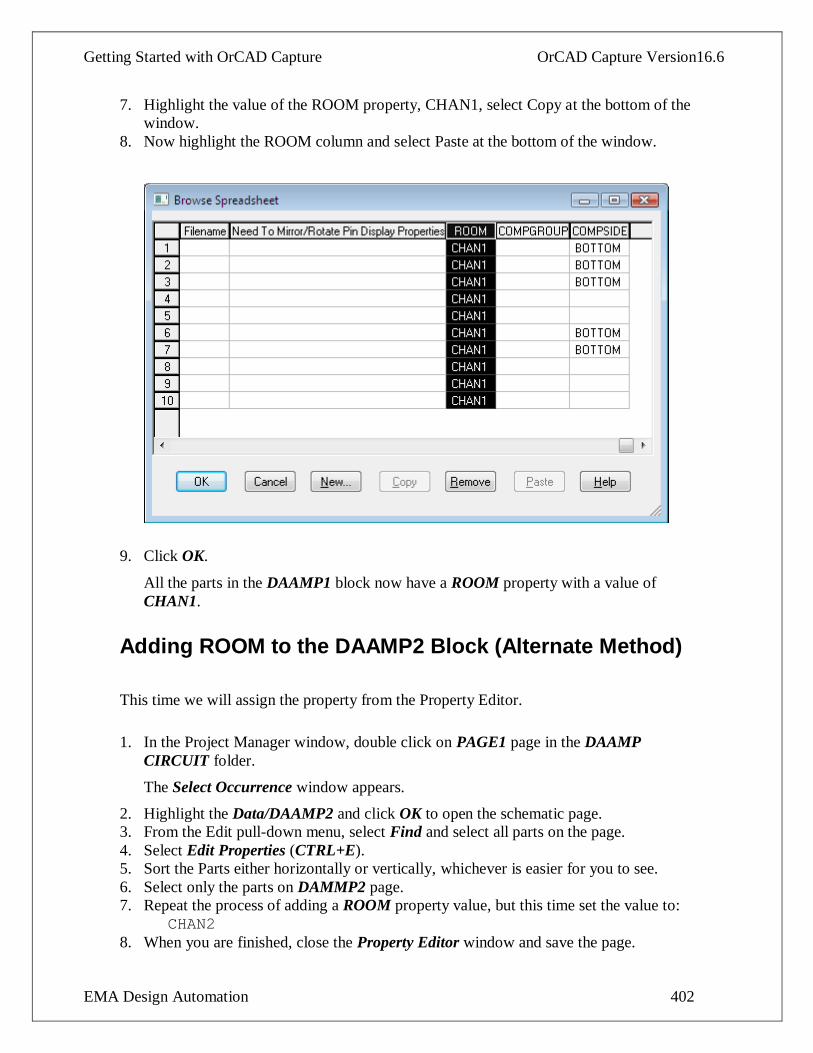
7. Highlight the value of the ROOM property, CHAN1, select Copy at the bottom of the
window.
8. Now highlight the ROOM column and select Paste at the bottom of the window.
9. Click OK.
All the parts in the DAAMP1 block now have a ROOM property with a value of
CHAN1.
Adding ROOM to the DAAMP2 Block (Alternate Method)
This time we will assign the property from the Property Editor.
1. In the Project Manager window, double click on PAGE1 page in the DAAMP
CIRCUIT folder.
The Select Occurrence window appears.
2. Highlight the Data/DAAMP2 and click OK to open the schematic page.
3. From the Edit pull-down menu, select Find and select all parts on the page.
4. Select Edit Properties (CTRL+E).
5. Sort the Parts either horizontally or vertically, whichever is easier for you to see.
6. Select only the parts on DAMMP2 page.
7. Repeat the process of adding a ROOM property value, but this time set the value to:
CHAN2
8. When you are finished, close the Property Editor window and save the page.
Getting Started with OrCAD Capture OrCAD Capture Version16.6
EMA Design Automation 403
Viewing the Occurrence Properties
1. To verify the changes, double click on PAGE1 page in the DAAMP Circuit folder.
The Select Occurrence window appears.
2. Click OK to open the Data/DAAMP2 schematic.
3. Resize the schematic window, and zoom to fit.
4. Select Edit - Find, and OK to select all parts on the page.
5. All the parts in the PAGE1 schematic are selected.
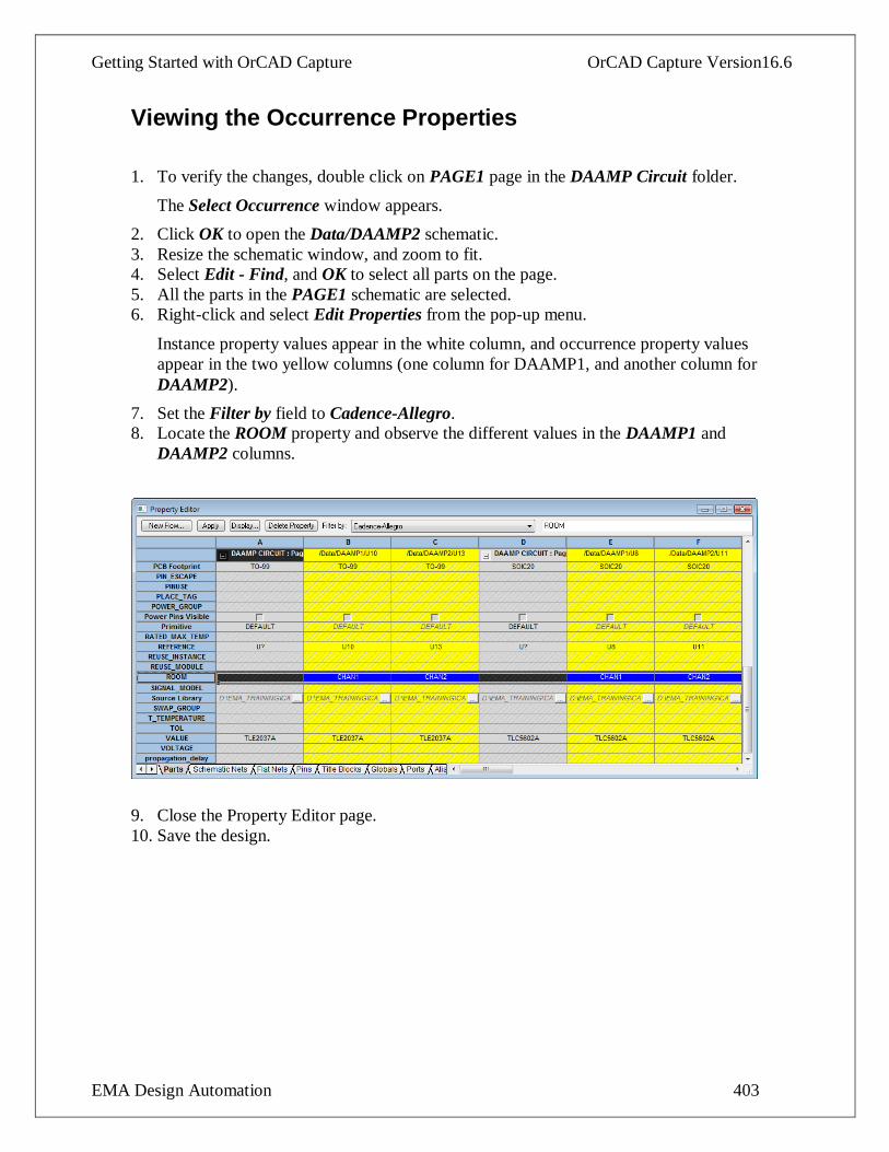
6. Right-click and select Edit Properties from the pop-up menu.
Instance property values appear in the white column, and occurrence property values
appear in the two yellow columns (one column for DAAMP1, and another column for
DAAMP2).
7. Set the Filter by field to Cadence-Allegro.
8. Locate the ROOM property and observe the different values in the DAAMP1 and
DAAMP2 columns.
9. Close the Property Editor page.
10. Save the design.
Getting Started with OrCAD Capture OrCAD Capture Version16.6
EMA Design Automation 404
Lab 20-2: Netlist for the OrCAD and
Allegro PCB Editor
Lab Objectives
After completing this lab you will be able to:
Create an OrCAD and Allegro PCB Editor netlist
View netlist files
Creating an OrCAD and Allegro PCB Editor Netlist
1. In the Project Manager, click on the design file and select Tools - Create Netlist.
2. Click the PCB Editor tab.
3. Click the Setup button in the upper right corner.
4. Click the browser button and navigate to the directory:
D:\<install directory>\tools\capture
5. Select the allegro.cfg file and click Open.
6. Click OK.
Getting Started with OrCAD Capture OrCAD Capture Version16.6
EMA Design Automation 405
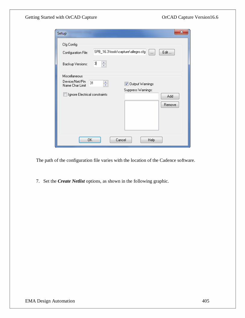
The path of the configuration file varies with the location of the Cadence software.
7. Set the Create Netlist options, as shown in the following graphic.

Getting Started with OrCAD Capture OrCAD Capture Version16.6
EMA Design Automation 406
8. Click OK.
9. Click Yes to create an allegro folder for the netlist files.
Observe that in the Project Manager window, the three OrCAD and Allegro PCB
Editor netlist files are listed in the Outputs folder.
Viewing the Netlist Files
1. In the Project Manager window, double click .\pstchip.dat.
This is the library definition file. Close the window.
2. In the Project Manager window, double click .\pstxnet.dat.
This is the nets and net properties file. Close the window.

Getting Started with OrCAD Capture OrCAD Capture Version16.6
EMA Design Automation 407
3. In the Project Manager window, double click .\pstxprt.dat.
This is the parts list and part properties file.
4. Close the netlist windows when you are done.
Closing the Training Project
1. Select File - Close.
This lesson did not generate inter-sheet references because this is a complex hierarchical
design. Inter-sheet references can be created for flat or simple hierarchical designs only.