led packaging market, technology and industry landscape · pdf filefromtechnologies to market...
TRANSCRIPT

From Technologies to Market
LED PACKAGING
-
Market, Technology and Industry Landscape
2017 Sample
Market and Technology ReportSource: Nasa

2
REPORT OBJECTIVES
This report serves to detail:
• LED industry and market status
• Process flows and technologies in LED packaging
• Recent LED packaging trends
• The importance of cost reduction in LED packaging
• Who is doing what
This report also provides market
• metrics at the LED material level
©2016 | www.yole.fr | LED Packaging 2017: Market, Technology and Industry Landscape | Sample

3
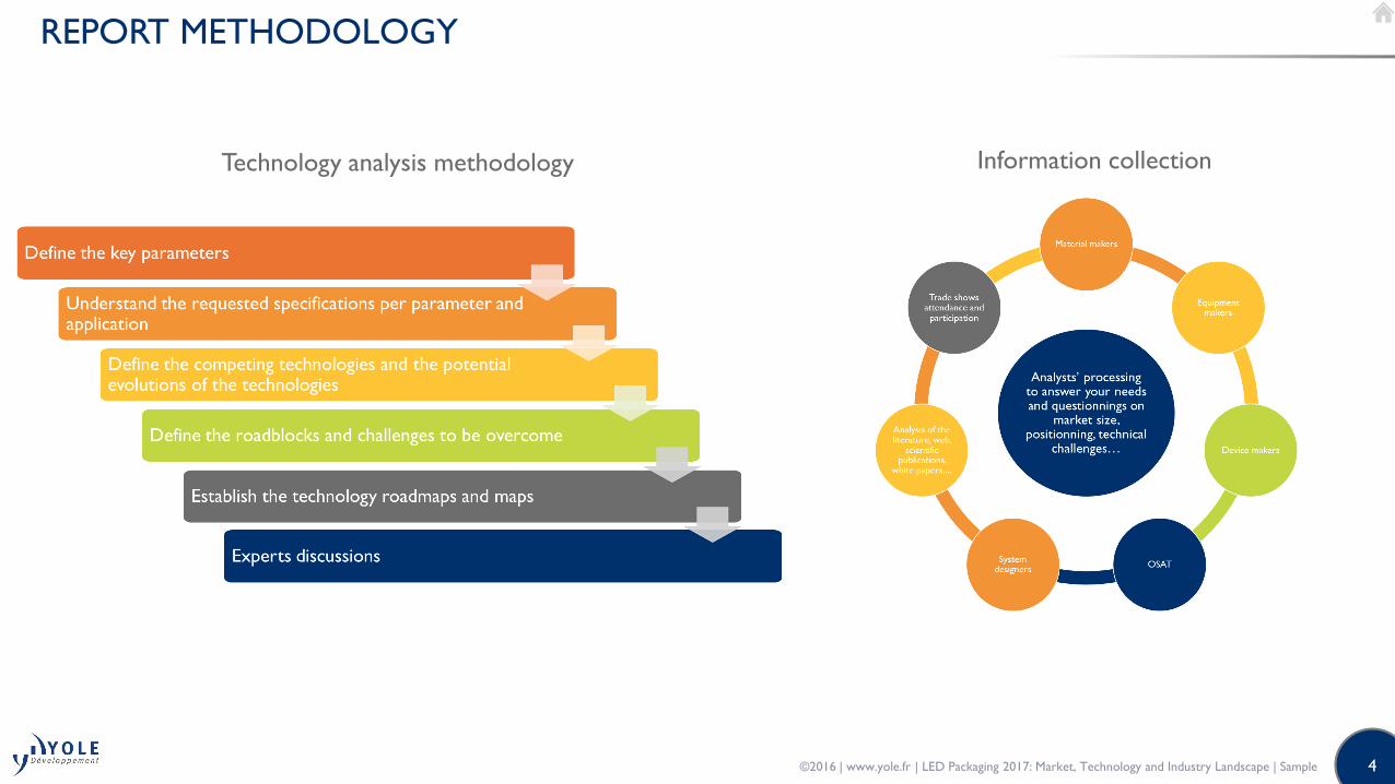
REPORT METHODOLOGY
Market segmentation methodology
Market forecast methodology
©2016 | www.yole.fr | LED Packaging 2017: Market, Technology and Industry Landscape | Sample
4
REPORT METHODOLOGY
Technology analysis methodology Information collection
©2016 | www.yole.fr | LED Packaging 2017: Market, Technology and Industry Landscape | Sample
5
o About the Author of the Report P8
o Glossary P9
o Executive Summary P10
o Status of the LED Industry (1/2) P35
LED Epitaxy Capacity Trends
• GaN MOCVD Capacity Evolution per Region (2010-2016)
• Top 10 Global LED Chip Manufacturers by Capacity
• Focus on China
• Top-20 LED Chipmakers In China
• Analysis
• GaN MOCVD Capacity Supply vs. Demand Trends
• Capacity and Wafer Start Geographic Breakdown
Packaged LED Market and Industry Trends
• Segmentation of Packaged LEDs
• History of LED Industry
• Market landscape
• Industrial Landscape
• Key Highlights
• Packaged LED Revenue Forecast - Split by Application
• Packaged LED Volume Forecast
• Split by Application
• Split by Package Type
• Split by Chip Type
• 2015 in a nutshell
• 2016 in a nutshell
• LED Market Trends
• Displays
• General Lighting
• Video Projector for Outdoor Display
• LED Packaging Companies Overview
o Status of the LED Industry (2/2) P35
Leading LED Packaging Companies / Regions
• Top-10 Players Revenue Analysis (2012 - 2015)
• 2015 Top-30 Players
• Market Shares Evolution per Region
• Trends
Zoom on Chinese Packaged LED Market and Industry
• Chinese Packaged LED Market and Industry Overview
• Top-30 LED Packaging Companies
• Overview
• Geographical Distribution
• 2015 Revenue
• Capacity (as of Q3-2016)
• Global Trends
Recent Trends in the Packaged LED Industry
• Overview
• Application Diversification - Automotive Lighting
• Vertical Integration - Module Level
• Vertical Integration - System Level
• Product Diversification - UV LEDs
• Product Diversification - IR LEDs
o LED Package Development (1/2) P78
Introduction
GaN-on-Si LEDs and GaN-on-GaN LEDs
• GaN-on-Si LEDs
• GaN-on-GaN LEDs
• Trends
Chip on Board (COB) LEDs
• Introduction
• Positioning - Package or Module?
• Drivers for Integration
TABLE OF CONTENT (1/6)
©2016 | www.yole.fr | LED Packaging 2017: Market, Technology and Industry Landscape | Sample

6
o LED Package Development (2/2) P78
Chip on Board (COB) LEDs
• Technology Trends
• High Density COB
• Spectrum Enhanced COB
• COB Evolution
• Industry
• Overview of Suppliers
• Main Areas of Development
• Manufacturing Process
• Market Segmentation and Uses
• COB LED Volume Forecast (2012 - 2021)
LED Filaments
• Overview
• Substrate Materials
• Manufacturing Process
• Performance and Cost
• Industry Trends
Flip Chip LEDs
• Introduction
• Benefits
• Key Players
• Applications
• TV
• Flash
• Automotive and General Lighting
• Flip Chip LED Volume Forecast (2012 - 2021)
Chip Scale Package (CSP) LEDs (1/2)
• Introduction
• Benefits
• CSP vs. Conventional Package
• Differences in CSP Architectures / Packages
Chip Scale Package (CSP) LEDs (2/2)
• CSP Cost Structure
• Low and Middle Power LEDs
• High Power LEDs
• Manufacturing Process
• Challenges
• Overview
• CSP Assembly onto Module / PCB
• Industry
• Key Players
• Highlights on US and European Manufacturers
• Highlights on Japanese Manufacturers
• Highlights on Korean Manufacturers
• Highlights on Taiwanese Manufacturers
• Highlights on Chinese Manufacturers
• Applications
• Flash
• Backlighting
• General Lighting
• Market Opportunities and Challenges
• CSP LED Volume Forecast (2012 - 2021)
o Overview of LED Packaging P144
The Functions of LED Packaging
Key Components of a Packaged LED
LED Packaging Typical Process Flow
Trends in GaN LED Chip Designs
Low and Middle Power LED Packaging
High Power LED Packaging
LED Package Power vs. Application
Cost Structure of Packaged LED
Supply Chain (Equipment and Material)
TABLE OF CONTENT (2/6)
©2016 | www.yole.fr | LED Packaging 2017: Market, Technology and Industry Landscape | Sample

7
o Wafer Bonding P158
Position in the Process Flow
Synthesis
Introduction
Process Selection
Technologies (Status, Trends and Alternatives)
Carrier Substrate
Equipment Suppliers
Miscellaneous - IP Aspects
o Substrate Removal P168
Position in the Process Flow
Synthesis
Introduction
Technologies
Laser Lift Off
• Overview
• Equipment Suppliers
• IP Aspects
• Yield Aspects
Chemical Lift Off
Other Techniques
The Case of GaAs-Based LEDs
o Die Singulation P180
Position in the Process Flow
Synthesis
Introduction
Overview of Die Singulation Techniques
Diamond Scribing
UV Laser Scribing
Scribing & Breaking - Comparison of Scribing Techniques
Blade Dicing
• Overview
• Advantages & Drawbacks
Laser Dicing / Ablation
• Overview
• Advantages & Drawbacks
• Focus on Serial Multibeam Laser Dicing
Stealth Dicing
• Overview
• Comparison with Traditional Dicing Techniques
Plasma Dicing
• Introduction
• Technologies of Panasonic and Plasma-Term
Global Benchmark of Dicing Technologies
Comparison of Die Singulation Technologies for LED
Cost Aspects
Dicing (and Backgrinding) Tape
Equipment Suppliers
Market Share by Technology
o Packaging Substrates (1/2) P205
Position in the Process Flow
Synthesis
Introduction
Low and Middle Power Packaged LEDs
• Overview
• New Materials (PCT, EMC, SMC and Ceramic)
High Power Packaged LEDs
• Thermal Management of High Power LEDs
• Leadframe Substrates
• Ceramic Substrates
• Choosing the Substrate Type
TABLE OF CONTENT (3/6)
©2016 | www.yole.fr | LED Packaging 2017: Market, Technology and Industry Landscape | Sample

8
o Packaging Substrates (2/2) P205
Chip On Board
• Substrate Comparison - MCPCB vs. Ceramic PCB
• COB vs. Package Substrate
Packaging Substrate Market
• Substrates vs. Circuit Board Material Options
• Choosing the Right Substrate
• High Power LED Substrate - Market Share by Substrate Type
• High Power LED Substrate Volume and Revenue Forecast (2012 -2021)
o ESD Protection P245
Position in the Process Flow
Synthesis
ESD / EOS Issues of High Power LEDs
Where are ESD / TVS Diodes Used?
Typical Symptom of ESD / EOS Damage
Zener / Avalanche Diodes
• Overview
• Illustration
• Trends
Zener / Avalanche Diodes Suppliers
Zener / Avalanche Diodes Volume and Revenue Forecast (2012 - 2021)
o Die Attach (1/2) P257
Position in the Process Flow
Synthesis
Introduction
Overview of Materials and Techniques
Resin / Adhesives
• Epoxy, Acrylic and Silicone
• Silver-Filled Epoxy
• Gold-Filled Epoxy
o Die Attach (1/2) P257
HMP Eutectic Soldering
• Au/Sn Solder Paste
• Metallization Techniques
• Flux Eutectic vs. Direct Eutectic
Silver Sintering
Potential Failure Associated to Die Attach
Comparison of Die Attach Techniques
• Gluing vs. Soldering
• Matching with Packaging Substrate
Die Attach Material vs. LED Package Power (and Applications)
Die Attach Technique vs. LED Package Type
Die Attach Material Volume and Revenue Forecast (2012 - 2021)
o Interconnections P286
Position in the Process
Synthesis
Overview
Wire Bonding
• Overview
• Comparison of Techniques
• Challenges
• Typical Failure
• Alternative - Ribbon Bonding
Flip Chip
• Overview
• Layout Principles and Technologies
• Main Techniques
• Underfill
• Trends
TABLE OF CONTENT (4/6)
©2016 | www.yole.fr | LED Packaging 2017: Market, Technology and Industry Landscape | Sample
9
o Encapsulation / Primary Optics P316
Position in the Process Flow
Synthesis
Introduction
Materials
• Overview
• Epoxy vs. Silicone
• Silicone (Overview and Comparison of Silicone Types)
Process
• Overview of Main Techniques
• Dispensing
• Molding
• Transfer vs. Compression Process
• Processability
• Comparison (Dispensing vs. Molding)
Interactions Encapsulant / Phosphors
• Overview
• Focus on Phosphor Sedimentation
• Focus on Chemical Compatibility
Failure Mechanisms
Material Suppliers (Overview, Analysis, Emerging Players & Recent Exits)
The Case of Packaged LED Lens
• Manufacturing Process
• Material
Trends
• Epoxy vs. Silicone
• Other Developments
Price Trends
Encapsulant Volume and Revenue Forecast (2012 - 2021)
Packaged LED Lens Material Volume and Revenue Forecast (2012 -2021)
o Phosphors (1/2) P350
Position in the Process Flow
Synthesis
The Different Ways to Generate White Light!
Key Requirements for LED Downconverters
LED Downconverters for Display Applications
LED Downconverters for Lighting Applications
Major White LED Designs
• Downconverter Combinations
• Trends
Configurations and Deposition Methods
On-Chip Configuration
• Overview
• Comparison
• The Case of CSP
Remote Phosphor
Material / Compositions
• Yellow Phosphors
• Green and Red Phosphors
• Focus on Garnets
• Focus on Silicates
• Focus on Nitrides and Oxynitrides
• Focus on Mn4+ Red Phosphors (PFS / KFS)
• Focus on “UV Chip + RGB Phosphor” Solutions
• Trends
• Timeline
• Application Matrix
Competitive Landscape
• Overview
• Focus on China
TABLE OF CONTENT (5/6)
©2016 | www.yole.fr | LED Packaging 2017: Market, Technology and Industry Landscape | Sample
10
o Phosphors (2/2) P350
Price Trends
• Introduction
• Focus on YAG and Nitrides
Quantum Dots
• Benefits & Challenges
• Display Applications
• Lighting Applications
Phosphor Volume Forecast (2012-2021) - Remote vs. On-Chip
Phosphor Revenue Forecast (2012-2021) - Split by Material
o Wafer Level Packaging P394
Synthesis
Overview
Manufacturing Status of WLP
True WLP
Technology Challenges
Trends
o Conclusion P402
o Appendix P406
TABLE OF CONTENT (6/6)
©2016 | www.yole.fr | LED Packaging 2017: Market, Technology and Industry Landscape | Sample

11
Biography & contact
ABOUT THE AUTHORS
Pars Mukish
Pars Mukish holds a master’s degree in Materials Science & Polymers (ITECH - France) and a master’s degree in Innovation &Technology Management (EM Lyon - France). Since 2015, he has overseen developing LED, OLED, and sapphire activities as aBusiness Unit Manager at Yole Développement. Previously, Pars worked for several years as a Marketing Analyst and Techno-Economic Analyst at the CEA (French Research Center).
©2016 | www.yole.fr | LED Packaging 2017: Market, Technology and Industry Landscape | Sample

12
Sample of the report
©2016 | www.yole.fr | LED Packaging 2017: Market, Technology and Industry Landscape | Sample

13
Total MOCVD capacity increased almost by a factor x5 since 2010 driven mostly by China (x25).
GaN MOCVD Capacity Evolution per Region (2010-2016)
LED EPITAXY CAPACITY TRENDS
©2016 | www.yole.fr | LED Packaging 2017: Market, Technology and Industry Landscape | Sample
14
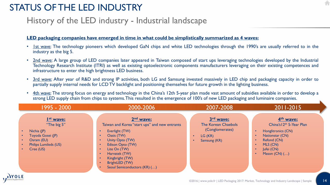
LED packaging companies have emerged in time in what could be simplistically summarized as 4 waves:
• 1st wave: The technology pioneers which developed GaN chips and white LED technologies through the 1990’s are usually referred to in theindustry as the big 5.
• 2nd wave: A large group of LED companies later appeared in Taiwan composed of start ups leveraging technologies developed by the IndustrialTechnology Research Institute (ITRI) as well as existing optoelectronic components manufacturers leveraging on their existing competences andinfrastructure to enter the high brightness LED business.
• 3rd wave: After year of R&D and strong IP activities, both LG and Samsung invested massively in LED chip and packaging capacity in order topartially supply internal needs for LCD TV backlight and positioning themselves for future growth in the lighting business.
• 4th wave: The strong focus on energy and technology in the China’s 12th 5-year plan made vast amount of subsidies available in order to develop astrong LED supply chain from chips to systems.This resulted in the emergence of 100’s of new LED packaging and luminaire companies.
History of the LED industry - Industrial landscape
STATUS OF THE LED INDUSTRY
1st wave:“The big 5”
• Nichia (JP)
• Toyoda Gosei (JP)
• Osram (EU)
• Philips Lumileds (US)
• Cree (US)
2nd wave:Taiwan and Korea “start ups” and new entrants
• Everlight (TW)
• Oasis (TW)
• Unity Opto (TW)
• Edison Opto (TW)
• Lite On (TW)
• Harvatek (TW)
• Kingbright (TW)
• BrightLED (TW)
• Seoul Semiconductors (KR) (…)
3rd wave:The Korean Chaebols
(Conglomerates)
• LG (KR)
• Samsung (KR)
4th wave:China’s12th 5-Year Plan
• Honglitronics (CN)
• Nationstar (CN)
• Refond (CN)
• MLS (CN)
• Jufei (CN)
• Mason (CN) (…)
1995 - 2000 2000-2006 2007-2008 2011-2015
©2016 | www.yole.fr | LED Packaging 2017: Market, Technology and Industry Landscape | Sample
15
Smart lighting will provide a further boost to lighting applications.
We expect “planned obsolescence” to become part of the luminaire maker strategy in consumer application.
LED Market Trends - General Lighting
STATUS OF THE LED INDUSTRY
• General lighting will drive LED demand.
• Strong penetration in outdoor and architectural lighting.
• Accelerating penetration in residential lighting.
• Better prospects than initially expected for LED as replacement of fluorescent tubes.
• Better prospects than expected in industrial lighting.
• Socket saturation won’t occur as fast as initially anticipated!
• Models usually assumed that because of the long lifetime of LEDs, the market will saturate once the majority of the light sockets havebeen converted… BUT:
• Actual lifetime is not as long as initially anticipated: 20,000-25,000 hours (or less) rather than 50,000 to 100,000 hours (initially quoted bythe industry).
• Smart lighting will trigger obsolescence in some markets.
• The availability of efficient, cheap and versatile light sources (LED) will increase the average consumption of artificial light per capita.
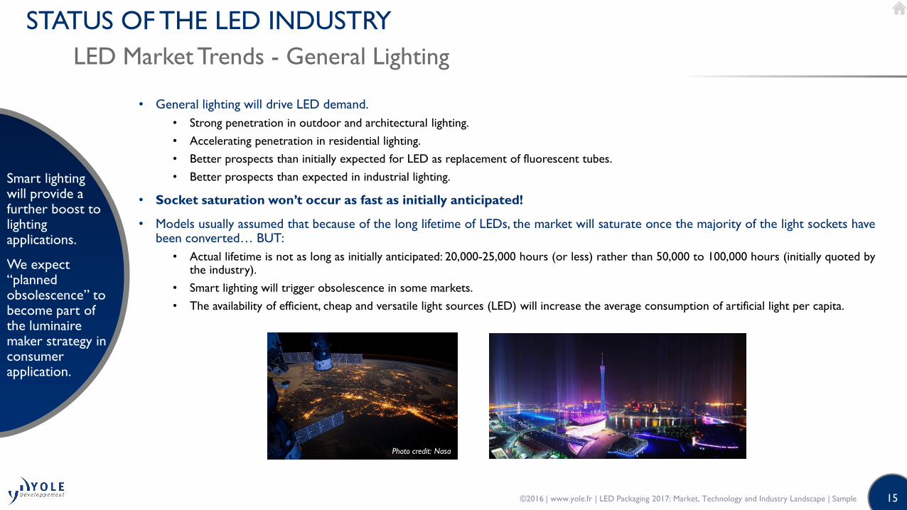
Photo credit: Nasa
©2016 | www.yole.fr | LED Packaging 2017: Market, Technology and Industry Landscape | Sample
16
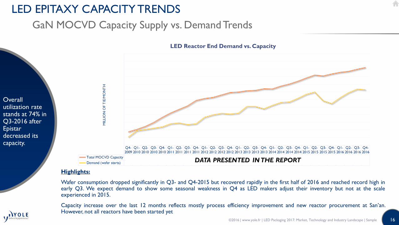
Overall utilization rate stands at 74% in Q3-2016 after Epistar decreased its capacity.
GaN MOCVD Capacity Supply vs. Demand Trends
LED EPITAXY CAPACITY TRENDS
Highlights:
Wafer consumption dropped significantly in Q3- and Q4-2015 but recovered rapidly in the first half of 2016 and reached record high inearly Q3. We expect demand to show some seasonal weakness in Q4 as LED makers adjust their inventory but not at the scaleexperienced in 2015.
Capacity increase over the last 12 months reflects mostly process efficiency improvement and new reactor procurement at San’an.However, not all reactors have been started yet
LED Reactor End Demand vs. Capacity
©2016 | www.yole.fr | LED Packaging 2017: Market, Technology and Industry Landscape | Sample
17
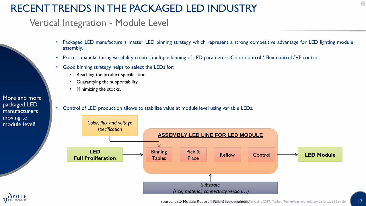
More and more packaged LED manufacturers moving to module level!
Vertical Integration - Module Level
RECENT TRENDS IN THE PACKAGED LED INDUSTRY
• Packaged LED manufacturers master LED binning strategy which represent a strong competitive advantage for LED lighting moduleassembly.
• Process manufacturing variability creates multiple binning of LED parameters: Color control / Flux control /VF control.
• Good binning strategy helps to select the LEDs for:
• Reaching the product specification.
• Guarantying the supportability.
• Minimizing the stocks.
• Control of LED production allows to stabilize value at module level using variable LEDs.
LED
Full Proliferation
Color, flux and voltage
specification
Substrate
(size, material, connectivity version…)
ASSEMBLY LED LINE FOR LED MODULE
Binning
Tables
Pick &
PlaceReflow Control LED Module
Source: LED Module Report - Yole Développement©2016 | www.yole.fr | LED Packaging 2017: Market, Technology and Industry Landscape | Sample

18
Most of the COB LED manufacturers are located in Asia.
Industry - Overview of Suppliers
COB LED
US:
Cree, Bridgelux, Lumileds (…)
+ 3 other players detailled in
the report
Russia:
XX
South Korea:
Seoul Semi., LG Innotek (…)
+ 6 other players detailled in the report
China:
Honglitronic, APT, CETC Huaying Electronics (…)
+ 17 other players detailled in the report
Germany:
Osram
Japan:
Sharp, Nichia, (…)
+ 4 other players
detailled in the report
Taiwan:
Edison Opto, Lextar,
Everlight (…)
+ 14 other players
detailled in the report
Finland:
XX
©2016 | www.yole.fr | LED Packaging 2017: Market, Technology and Industry Landscape | Sample
19
While a dedicated supply chain has emerged, sapphire filaments are often produced from rejected LED wafers.
Manufacturing Process (1/2)
LED FILAMENT
• The filament substrates typical dimension is: 30 (L) * 0.8 (W) * 0.4 to 0.8 (thickness) mm.
• They were initially cut with wire saws from 2” sapphire wafers (in many cases, reject from production for LED substrates).
• As demand increased, a dedicated supply chain emerged: many suppliers now start from a rectangular brick which is then sliced intoindividual window blanks before double side polishing. Laser cutting has replaced diamond wire saws.
• The filaments are then assembled onto a lead frame to facilitate subsequent processing for the manufacturing of the COB-typefilament (silver electrode metallization, die attach, interconnect, phosphor coating…).
Sapphire filament substrates
Picture: Zhejiang Terios New Energy
Finished and assembled LED filaments
Picture: Tevaja
©2016 | www.yole.fr | LED Packaging 2017: Market, Technology and Industry Landscape | Sample
20
Compared to MESA and vertical structures, Flip Chip LED can offer advantages toward reliability and lifetime, luminous output, package size and manufacturing cost.
Benefits (1/2)
FLIP CHIP LED
• Flip Chip (FC) LED manufacturing process use (in most case) a gold-tin eutectic direct bonding method where the chip is “stuck” onto the package substrate.
• Such structure of package allow for several features compared to MESA and vertical LEDs which have some unavoidabledisadvantages, such as faulty wire weld, surge strike, insufficient resistance to high current, bond wire breakage caused by the thermalexpansion and contraction of packaging silicone, yield affected by bond wire in manufacturing process (…).
No Wire Bonding
Reduce LEDs damage risk1
Increase light emitting area
Reduce package size
Low Sheet Resistance
/ Low Driving Current Allow for better thermal dissipation
Low Thermal
ResistanceAllows for high electrical currents
Flip Chip
LED
-
Direct
Bumping
or Eutectic
Bonding
Increase of reliability
and lifetime
Increase of luminosity
(with increased
operating efficiency)
Potential increase of
lm/W and lm/$
Decrease of package
size and allow for new
package structure
1. As gold wire can break during LED manufacturing process, under LED operation with huge temperature differences (…).
©2016 | www.yole.fr | LED Packaging 2017: Market, Technology and Industry Landscape | Sample

21
• Nichia has developed a CSP architecture to enable light output only on top of the LED contrary to other LED manufacturers.
• It allow to place the LEDs close to each other on the PCB because there is no side emission of the light and therefore no mutual absorption of light.
• Gap between LED can be reduced to 0.2mm compared to 1mm for conventional CSP LEDs.
• Following Nichia statement, there is no color shifting contrary to other CSP LEDs.
Differences in CSP Architectures / Packages
CSP LED
Difference between Nichia and conventional CSP architecture
Source: Nichia
• Seoul Semiconductor has developed its own CSP architecture that is simpler than conventional CSPdesign since there is no ceramic substrate.
• WICOP (Wafer Level Integrated Chip on PCB) is designed to directly connect the chip to the PCB as thereis no intermediate substrate.
• As the LED chip is directly connected onto the PCB, hence its thermal dissipation channel is especiallyshort, and has low thermal resistance. As a result, the driving current is double that of the average LEDpackage.
• Even if there are some differences between CSP LED manufacturers in the architecture of the “package”,all CSP LEDs have no need for main parts such as package or wire bonding.
Difference between Seoul
Semiconductor CSP and conventional
CSP architecture
Source: Seoul Semiconductor
©2016 | www.yole.fr | LED Packaging 2017: Market, Technology and Industry Landscape | Sample

22
LED Packaging Process Flow
OVERVIEW OF LED PACKAGING
Epiwafer
Carrier wafer
Epitaxial
substrate
Die
Lens
Carrier wafer
MESA
&
Vertical
Flip
Chip
LEGEND
Only for vertical LED
packaging
Can be “mixed” with
interconnection for Flip
Chip LED packaging
©2016 | www.yole.fr | LED Packaging 2017: Market, Technology and Industry Landscape | Sample

23
For both GaAs-based and Sapphire-based LEDs, wafer bonding enables improved thermal, electrical and/or optical properties.
Introduction (2/2)
WAFER BONDING
• In such designs (i.e.:VTF and TFFC LEDs), Sapphire is replaced by another carrier that offers higher thermal conductivity:
• Silicon-based LEDs involve also the transfer to a silicon carrier (i.e.: bonding step) and removal of the original Siliconsubstrate. Indeed, unlike Sapphire which is transparent, Silicon re-absorbs most of the light emitted toward the substrate.This significantly decreases the efficiency of the LED. The most common solution to the problem is to use a vertical LED structure:
• Regarding GaN-based LEDs (i.e.: GaN-on-GaN LEDs), no wafer bonding process is required.
Epitaxy Substrate
LED Epitaxial Layers
1. LED epiwafer
Bonding Layer
Bonding Layer
Carrier substrate
Epitaxy Substrate
LED Epitaxial Layers
Bonding Layer
Carrier substrate
LED Epitaxial Layers Bonding layer
Carrier substrate
LED Epitaxial Layers
4. VTF LED structure
Bonding Layer
n-contact pad
Epitaxy Substrate
LED Epitaxial LayersBonding Layer
Bonding Layer
Carrier substrate
Epitaxy Substrate
LED Epitaxial Layers
Bonding Layer
Carrier substrate
LED Epitaxial Layers Bonding layer
Carrier substrate
LED Epitaxial Layers
Bonding Layer
n-contact padTypical process flow of Vertical
Thin Film (VTF) LED
manufacturing
n-GaN
p-GaN
Epitaxy Substrate (Si)
Mirror layer
Carrier substrate (Si)
n-GaN
p-GaN
Epitaxy Substrate (Si)
Mirror layer
n-GaN
p-GaN Active layers
Epitaxy
Substrate (Si)
Emitted light
Absorbed light
n-GaN
p-GaN
Mirror layer
Carrier substrate (Si)
1. LED-on-Si 2. Mirror layer deposition 3. Carrier substrate bonding 4. Substrate removal
Bonding and removal
process for LED-On-Si
2. Carrier substrate bonding 3. Substrate removal
©2016 | www.yole.fr | LED Packaging 2017: Market, Technology and Industry Landscape | Sample

24
LLO is the most common substrate removal technique used for volume manufacturing. However, IP constraints, cost, performance limitations and damage caused to the epilayer provide incentive for the development of alternatives.
Other Techniques
SUBSTRATE REMOVAL
• We have identified 3 new techniques for substrate removal but current performance (development status) are not sufficient yet todirectly compete with LLO.
Technique Developer Comments
Chemical Mechanical
PlanarizationASTRI
• The process uses standard grinding and polishing combined with “polish stops”
structures made of hard material embedded into the structure to protect the
epi layers.
• Potentially, multiple wafers can be processed in batch.Also, there is less patent
issues than for LLO. And an increase of yield in terms of reverse current
specification can be achieved compared to LLO.
Electrochemical EtchingYale
University
• Substrate removal technique based on the creation of a nanoporous layer of
GaN using an electrochemical etcher. Further nitride layers are then grown. A
new substrate can then be applied to the top of the structure and the growth
substrate removed at the weakened nanoporous region.
Mechanical TransferNTT
• NTT has developed a technique for growing high-quality layered BN thin films
on sapphire substrates, and also growing high-quality GaN-based thin films on
BN. Since in this structure the cleavable BN plays the role of a release layer, one
can easily detach the GaN-based thin-film devices from the sapphire substrates
and transfer them to the other substrate.
More details on these Other Techniques
given in appendix
©2016 | www.yole.fr | LED Packaging 2017: Market, Technology and Industry Landscape | Sample

25
Global Benchmark of Dicing Technologies (i.e.: Not LED-Centric) (1/2)
DIE SINGULATION
Blade Dicing Laser Ablation Stealth Dicing Plasma Dicing
Upfront cost $200k XX XX
Cost of
Ownership (CoO)Medium XX Medium XX
Technology type Chipping Chipping No chipping No chipping
Debris Dust XX Dust-free XX
Water XX Required No water / cleaning required XX
Die strength Low XX Medium XX
Production yield Dicing line limitation Not so good: Line limitation Low kerf loss better yield High productivity
Thermal effect on
the deviceHeat effect Heat effect Unaffected Heat-free
Wafer breakage Breakage strength Wafer breakage Superior breakage strength Chip strength: > 3,000 MPa
Main Advantages• Standard process suitable for thick
wafer (> 250µm)• XX
• Clean process
• XX
• XX
• High level device strength
• Independent of die size
• XX
• XX
Main Drawbacks
• Dirty process
• Crack propagation
• Increased damage for thinner wafers
and small die
• XX
• Lateral damage
• XX
• Scratch on the surface > 200 µm
• XX
• XX
• Heat propagation can damage the die
• Disruptive technology
• XX
©2016 | www.yole.fr | LED Packaging 2017: Market, Technology and Industry Landscape | Sample

26
The diversity of LED structures, power levels, applications and process equipment considerations require different die attach solutions to optimize cost and performance aspects.
Die Attach Material vs. LED Package Power (and Applications)
DIE ATTACH
ApplicationThermal ConductivityDie Attach Material
LEGEND
LOW POWER SUPER HIGH POWERHIGH POWERMIDDLE POWER
XX
XXXX, XX, XX
LED Downlight
XX
Automotive Exterior Lighting (DRL, Tail, Signal)
Auto Head Lamp
T8 Tube Lamps
7 - XX W/mK
XX - XX W/mK > 200 W/mKXX - 200 W/mK
• XX
• XX
• Silver-Filled Epoxy
• XX
Pressure-Assisted Sintered
Ag
Pressureless Sintered Ag
XX
Perf
orm
an
ce (
Th
erm
al
an
d R
eliab
ilit
y)
0 - 0.3W > 4W1 - 4W0.3 - 1W
Source: Yole Développement / Alpha
©2016 | www.yole.fr | LED Packaging 2017: Market, Technology and Industry Landscape | Sample

27
• White light from packaged LEDs is generated by combining blue photons from LED chips with photons of other colors from phosphor material(s).However, as phosphors are mostly produced as powders, LED manufacturers have to blend it the encapsulant to suspend the phosphor powderand allow for simple deposition onto the blue LED chip.
• Many encapsulating materials are available on the market with a wide variety of physical and performance characteristics. LED packagers evaluateperformance of such materials along optical, mechanical, chemical and thermal metrics (with some figures of merit bearing more importance tothe overall package performance than others).
• Additionally, they have to make sure that such material will have the best fit with the phosphor used.
• Below are presented key parameters to consider for encapsulant and potential associated interactions with phosphor materials.
Interactions Encapsulant / Phosphors - Overview
ENCAPSULATION / PRIMARY OPTICS
KEY PARAMETERS
OF
INTERACTIONS
BETWEEN
ENCAPSULANT
AND PHOPSHORS
OPTICAL PROPERTIES
MECHANICAL PROPERTIES
CHEMICAL COMPATIBILITY
THERMAL CONDUCTIVITY
CURING PROCESS
More details on Each Parameter of
Interactions in appendix
©2016 | www.yole.fr | LED Packaging 2017: Market, Technology and Industry Landscape | Sample

28
Encapsulant material should represent a market volume of ~XX Metric Tons by 2021, mostly driven by Methyl Silicone (and Phenyl Silicone) materials.
EncapsulantVolume Forecast (2012-2021)
ENCAPSULATION / PRIMARY OPTICS
©2016 | www.yole.fr | LED Packaging 2017: Market, Technology and Industry Landscape | Sample

29
Phosphor quantity can vary significantly from one type of package to another.
On-Chip Configuration - Overview
PHOSPHORS
• Downconverters are usually mixed with a binder (Silicone, Epoxy) and deposited on the device. Alternatively, they can be in a ceramicform or embedded into a solid-state binder that is paired with phosphor chips afterwards (e.g.: glass).The major types are:
Increasing phosphor packing density
Casting (Dispersion): XX
CREE Osram
Conformal Coating Package level:
Conformal Coating or Pre-Form – Chip only:
Philips LumiledsPicture: System Plus Consulting
Volume conversion On-Chip conversion
Cost efficient but:
• Particle segregation, binder viscosity hard to control.
• XX
• XX
For XX and XX power packages.
Better color uniformity & XX (especially withceramics) but more expensive.
2014: Mostly for XX packages.
2015+: Increased adoption in XX.
©2016 | www.yole.fr | LED Packaging 2017: Market, Technology and Industry Landscape | Sample
30
Silicates were developed as an alternative to YAG and will lose ground as YAG IP falls into public domain.
Material / Compositions - Focus on Silicates
PHOSPHORS
• M2SiO4:Eu2+ (M=Ba, Sr, Ca) phosphors were originally studied in the 60’s.
• Compositions for LEDs silicate phosphors and the associated intellectual property has beenasserted by a group called the BOSE consortium, consisting of Tridonic, LeuchtstoffwerkBreitungen (LWB) and Litec (now part of Merck) all assignees on the fundamentalUS6809347 silicate patent. The consortium later added Toyoda Gosei which extended theclaims.
• The BOSE consortium later signed a cross licensing agreement with Intematix. Attempt bythe consortium to trademark the name BOSE for phosphors was denied after a complaintby electronic audio company Bose.
• Other companies like GE and Osram also own some IP on silicate phosphors for LEDs.
• Compositions have been developed to cover the green and red portions of the spectra,from 500 to more than 610 nm. However, thermal quenching and chemical instability areoften issues for the most extreme wavelength.
• Significant progress has been made on those aspects. Various types of coating have beenused to improve stability and performance have improved on a continuous basis.Performance of the best silicates are now approaching those of Yellow/Green YAGphosphors. However, those higher performance silicates come at a cost premium.
• Yellow silicates are being quickly displaced by YAG. Green silicates remain used in displayapplications. Orange silicates offer a cheaper alternative to some nitride for mid power LEDwhere photon flux and operating temperature are not too high.
Companies constituting the BOSE consortium
or having cross licensing agreement on silicates
©2016 | www.yole.fr | LED Packaging 2017: Market, Technology and Industry Landscape | Sample
31
RELATED REPORTS
Discover more related reports
within our bundles here.©2016 | www.yole.fr | LED Packaging 2017: Market, Technology and Industry Landscape | Sample

ORDER FORMLED Packaging 2017: Market, Technology and Industry Landscape
SHIPPING CONTACT
First Name:
Email:
Last Name:
Phone:
PAYMENT
BY CREDIT CARD Visa Mastercard Amex
Name of the Card Holder:
Credit Card Number:
Card Verification Value (3 digits except AMEX: 4 digits):
Expiration date:
BY BANK TRANSFERBANK INFO: HSBC, 1 place de la Bourse, F-69002 Lyon, France, Bank code: 30056, Branch code: 00170Account No: 0170 200 1565 87, SWIFT or BIC code: CCFRFRPP, IBAN: FR76 3005 6001 7001 7020 0156 587
RETURN ORDER BY • FAX: +33 (0)472 83 01 83• MAIL: YOLE DÉVELOPPEMENT, Le Quartz,
75 Cours Emile Zola, 69100 Villeurbanne/Lyon - France
SALES CONTACTS • North America - Steve Laferriere: +13106 008 267
[email protected] • Europe & RoW - Lizzie Levenez: + 49 15 123 544 182
[email protected]• Japan & Rest of Asia - Takashi Onozawa: +81 3 6869 6970
[email protected] • Greater China - Mavis Wang: +886 979 336 809
[email protected]• Specific inquiries: +33 472 830 180 – [email protected]
(1) Our Terms and Conditions of Sale are available at www.yole.fr/Terms_and_Conditions_of_Sale.aspx The present document is valid 24 months after its publishing date: December 14, 2016
/
ABOUT YOLE DEVELOPPEMENT
BILL TO
Name (Mr/Ms/Dr/Pr):
Job Title:
Company:
Address:
City:
State:
Postcode/Zip:
Country*:
*VAT ID Number for EU members:
Tel:
Email:
Date:
PRODUCT ORDER
Please enter my order for above named report: One user license*: Euro 5,490 Multi user license: Euro 6,490- The report will be ready for delivery from December 14, 2016- For price in dollars, please use the day’s exchange rate. All reports are
delivered electronically at payment reception. For French customers, add 20% for VAT
I hereby accept Yole Développement’s Terms and Conditions of Sale(1)
Signature:
*One user license means only one person at the company can use the report.
Founded in 1998, Yole Développement has grown to become a group of companies providing marketing, technology and strategy consulting, media in addition to corporate finance services. With a strong focus on emerging applications using silicon and/or micro manufacturing (technology or process), Yole Développement group has expanded to include more than 50 associates worldwide covering MEMS, Compound Semiconductors, LED, Image Sensors, Optoelectronics, Microfluidics & Medical, Photovoltaics, Advanced Packaging, Manufacturing, Nanomaterials and Power Electronics. The group supports industrial companies, investors and R&D organizations worldwide to help them understand markets and follow technology trends to develop their business.
MEDIA & EVENTS• i-Micronews.com, online disruptive technologies website• @Micronews, weekly e-newsletter• Communication & webcasts services• Events: Yole Seminars, Market Briefings…More information on www.i-micronews.com
CONTACTSFor more information about :• Consulting Services: Jean-Christophe Eloy ([email protected])• Financial Services: Jean-Christophe Eloy ([email protected])• Report Business: Fayçal Khamassi ([email protected])• Press relations: Sandrine Leroy ([email protected])
CONSULTING• Market data & research, marketing analysis• Technology analysis• Reverse engineering & costing services• Strategy consulting• Patent analysisMore information on www.yole.fr
REPORTS• Collection of technology & market reports• Manufacturing cost simulation tools• Component reverse engineering & costing
analysis• Patent investigationMore information on www.i-micronews.com/reports
FINANCIAL SERVICES• Mergers & Acquisitions• Due diligence• FundraisingMore information on Jean-Christophe Eloy ([email protected])
Definitions: “Acceptance”: Action by which the Buyer accepts the terms and conditions of sale in their entirety. It is done by signing the purchase order which mentions “I hereby accept Yole’s Terms and Conditions of Sale”.
“Buyer”: Any business user (i.e. any person acting in the course of its business activities, for its business needs) entering into the following general conditions to the exclusion of consumers acting in their personal interests.
“Contracting Parties” or “Parties”: The Seller on the one hand and the Buyer on the other hand.
“Intellectual Property Rights” (“IPR”) means any rights held by the Seller in its Products, including any patents, trademarks, registered models, designs, copyrights, inventions, commercial secrets and know-how, technical information, company or trading names and any other intellectual property rights or similar in any part of the world, notwithstanding the fact that they have been registered or not and including any pending registration of one of the above mentioned rights.
“License”: For the reports and databases, 3 different licenses are proposed. The buyer has to choose one license:• One user license: one person at the company can use the report.• Multi-user license: the report can be used by unlimited users
within the company. Subsidiaries and Joint-Ventures are not included.
• Corporate license: purchased under “Annual Subscription” program, the report can be used by unlimited users within the company. Joint-Ventures are not included.
“Products”: Depending on the purchase order, reports or database on MEMS, CSC, Optics/MOEMS, Nano, bio… to be bought either on a unit basis or as an annual subscription. (i.e. subscription for a period of 12 calendar months). The annual subscription to a package (i.e. a global discount based on the number of reports that the Buyer orders or accesses via the service, a global search service on line on I-micronews and a consulting approach), is defined in the order. Reports are established in PowerPoint and delivered on a PDF format and the database may include Excel files.
“Seller”: Based in Lyon (France headquarters), Yole Développement is a market research and business development consultancy company, facilitating market access for advanced technology industrial projects. With more than 20 market analysts, Yole works worldwide with the key industrial companies, R&D institutes and investors to help them understand the markets and technology trends.
1. SCOPE 1.1 The Contracting Parties undertake to observe the following
general conditions when agreed by the Buyer and the Seller. ANY ADDITIONAL, DIFFERENT, OR CONFLICTING TERMS AND CONDITIONS IN ANY OTHER DOCUMENTS ISSUED BY THE BUYER AT ANY TIME ARE HEREBY OBJECTED TO BY THE SELLER, SHALL BE WHOLLY INAPPLICABLE TO ANY SALE MADE HEREUNDER AND SHALL NOT BE BINDING IN ANY WAY ON THE SELLER.
1.2 This agreement becomes valid and enforceable between the Contracting Parties after clear and non-equivocal consent by any duly authorized person representing the Buyer. For these purposes, the Buyer accepts these conditions of sales when signing the purchase order which mentions “I hereby accept Yole’s Terms and Conditions of Sale”. This results in acceptance by the Buyer.
1.3 Orders are deemed to be accepted only upon written acceptance and confirmation by the Seller, within [7 days] from the date of order, to be sent either by email or to the Buyer’s address. In the absence of any confirmation in writing, orders shall be deemed to have been accepted.
2. MAILING OF THE PRODUCTS 2.1 Products are sent by email to the Buyer:
• within [1] month from the order for Products already released; or • within a reasonable time for Products ordered prior to their effective release. In this case, the Seller shall use its best endeavours to inform the Buyer of an indicative release date and the evolution of the work in progress.
2.2 Some weeks prior to the release date the Seller can propose a pre-release discount to the Buyer The Seller shall by no means be responsible for any delay in respect of article 2.2 above, and including incases where a new event or access to new contradictory information would require for the analyst extra time to compute or compare the data in order to enable the Seller to deliver a high quality Products.
2.3 The mailing of the Product will occur only upon payment by the Buyer, in accordance with the conditions contained in article 3.
2.4. The mailing is operated through electronic means either by email via the sales department or automatically online via an email/password. If the Product’s electronic delivery format is defective, the Seller undertakes to replace it at no charge to the Buyer provided that it is informed of the defective formatting within 90 days from the date of the original download or receipt of the Product.
2.5 The person receiving the Products on behalf of the Buyer shall immediately verify the quality of the Products and their conformity to the order. Any claim for apparent defects or for non-conformity shall be sent in writing to the Seller within 8 days of receipt of the Products. For this purpose, the Buyer agrees to produce sufficient evidence of such defects. .
2.6 No return of Products shall be accepted without prior information to the Seller, even in case of delayed delivery. Any Product returned to the Seller without providing prior information to the Seller as required under article 2.5 shall remain at the Buyer’s risk.
3. PRICE, INVOICING AND PAYMENT 3.1 Prices are given in the orders corresponding to each Product
sold on a unit basis or corresponding to annual subscriptions. They are expressed to be inclusive of all taxes. The prices may be reevaluated from time to time. The effective price is deemed to be the one applicable at the time of the order.
3.2 Yole may offer a pre release discount for the companies willing to acquire in the future the specific report and agreeing on the fact that the report may be release later than the anticipated release date. In exchange to this uncertainty, the company will get a discount that can vary from 15% to 10%.
3.3 Payments due by the Buyer shall be sent by cheque payable to Yole Développement, credit card or by electronic transfer to the following account: HSBC, 1 place de la Bourse 69002 Lyon France Bank code: 30056 Branch code: 00170 Account n°: 0170 200 1565 87BIC or SWIFT code: CCFRFRPP IBAN: FR76 3005 6001 7001 7020 0156 587
To ensure the payments, the Seller reserves the right to request down payments from the Buyer. In this case, the need of down payments will be mentioned on the order. 3.4 Payment is due by the Buyer to the Seller within 30 days
from invoice date, except in the case of a particular written agreement. If the Buyer fails to pay within this time and fails to contact the Seller, the latter shall be entitled to invoice interest in arrears based on the annual rate Refi of the «BCE» + 7 points, in accordance with article L. 441-6 of the French Commercial Code. Our publications (report, database, tool...) are delivered only after reception of the payment.
3.5 In the event of termination of the contract, or of misconduct, during the contract, the Seller will have the right to invoice at the stage in progress, and to take legal action for damages.
4. LIABILITIES 4.1 The Buyer or any other individual or legal person acting on
its behalf, being a business user buying the Products for its business activities, shall be solely responsible for choosing the Products and for the use and interpretations he makes of the documents it purchases, of the results he obtains, and of the advice and acts it deduces thereof.
4.2 The Seller shall only be liable for (i) direct and (ii) foreseeable pecuniary loss, caused by the Products or arising from a material breach of this agreement
4.3 In no event shall the Seller be liable for: a) damages of any kind, including without limitation, incidental or consequential damages (including, but not limited to, damages for loss of profits, business interruption and loss of programs or information) arising out of the use of or inability to use the Seller’s website or the Products, or any information provided on the website, or in the Products; b) any claim attributable to errors, omissions or other inaccuracies in the Product or interpretations thereof.
4.4 All the information contained in the Products has been obtained from sources believed to be reliable. The Seller does not warrant the accuracy, completeness adequacy or reliability of such information, which cannot be guaranteed to be free from errors.
4.5 All the Products that the Seller sells may, upon prior notice to the Buyer from time to time be modified by or substituted with similar Products meeting the needs of the Buyer. This modification shall not lead to the liability of the Seller, provided that the Seller ensures the substituted Product is similar to the Product initially ordered.
4.6 In the case where, after inspection, it is acknowledged that the Products contain defects, the Seller undertakes to replace the defective products as far as the supplies allow and without indemnities or compensation of any kind for labor costs, delays, loss caused or any other reason. The replacement is guaranteed for a maximum of two months starting from the delivery date. Any replacement is excluded for any event as set out in article 5 below.
4.7 The deadlines that the Seller is asked to state for the mailing of the Products are given for information only and are not guaranteed. If such deadlines are not met, it shall not lead to any damages or cancellation of the orders, except for non acceptable delays exceeding [4] months from the stated deadline, without information from the Seller. In such case only, the Buyer shall be entitled to ask for a reimbursement of its first down payment to the exclusion of any further damages.
4.8 The Seller does not make any warranties, express or implied, including, without limitation, those of sale ability and fitness for a particular purpose, with respect to the Products. Although the Seller shall take reasonable steps to screen Products for infection of viruses, worms, Trojan horses or other codes containing contaminating or destructive properties before making the Products available, the Seller cannot guarantee that any Product will be free from infection.
5. FORCE MAJEURE The Seller shall not be liable for any delay in performance directly or indirectly caused by or resulting from acts of nature, fire, flood, accident, riot, war, government intervention, embargoes, strikes, labor difficulties, equipment failure, late deliveries by suppliers or other difficulties which are beyond the control, and not the fault of the Seller.
6. PROTECTION OF THE SELLER’S IPR 6.1 All the IPR attached to the Products are and remain the
property of the Seller and are protected under French and international copyright law and conventions.
6.2 The Buyer agreed not to disclose, copy, reproduce, redistribute, resell or publish the Product, or any part of it to any other party other than employees of its company. The Buyer shall have the right to use the Products solely for its own internal information purposes. In particular, the Buyer shall therefore not use the Product for purposes such as: • Information storage and retrieval systems; • Recordings and re-transmittals over any network (including
any local area network); • Use in any timesharing, service bureau, bulletin board or
similar arrangement or public display; • Posting any Product to any other online service (including
bulletin boards or the Internet);• Licensing, leasing, selling, offering for sale or assigning the
Product. 6.3 The Buyer shall be solely responsible towards the Seller of
all infringements of this obligation, whether this infringement comes from its employees or any person to whom the Buyer has sent the Products and shall personally take care of any related proceedings, and the Buyer shall bear related financial consequences in their entirety.
6.4 The Buyer shall define within its company point of contact for the needs of the contract. This person will be the recipient of each new report in PDF format. This person shall also be responsible for respect of the copyrights and will guaranty that the Products are not disseminated out of the company.
6.5 In the context of annual subscriptions, the person of contact shall decide who within the Buyer, shall be entitled to access on line the reports on I-micronews.com. In this respect, the Seller will give the Buyer a maximum of 10 password, unless the multiple sites organization of the Buyer requires more passwords. The Seller reserves the right to check from time to time the correct use of this password.
6.6 In the case of a multisite, multi license, only the employee of the buyer can access the report or the employee of the companies in which the buyer have 100% shares. As a matter of fact the investor of a company, the joint venture done with a third party etc..cannot access the report and should pay a full license price.
7. TERMINATION 7.1 If the Buyer cancels the order in whole or in part or postpones
the date of mailing, the Buyer shall indemnify the Seller for the entire costs that have been incurred as at the date of notification by the Buyer of such delay or cancellation. This may also apply for any other direct or indirect consequential loss that may be borne by the Seller, following this decision.
7.2 In the event of breach by one Party under these conditions or the order, the non-breaching Party may send a notification to the other by recorded delivery letter upon which, after a period of thirty (30) days without solving the problem, the non-breaching Party shall be entitled to terminate all the pending orders, without being liable for any compensation.
8. MISCELLANEOUS All the provisions of these Terms and Conditions are for the benefit of the Seller itself, but also for its licensors, employees and agents. Each of them is entitled to assert and enforce those provisions against the Buyer. Any notices under these Terms and Conditions shall be given in writing. They shall be effective upon receipt by the other Party. The Seller may, from time to time, update these Terms and Conditions and the Buyer, is deemed to have accepted the latest version of these terms and conditions, provided they have been communicated to him in due time.
9. GOVERNING LAW AND JURISDICTION 9.1 Any dispute arising out or linked to these Terms and
Conditions or to any contract (orders) entered into in application of these Terms and Conditions shall be settled by the French Commercial Courts of Lyon, which shall have exclusive jurisdiction upon such issues.
9.2 French law shall govern the relation between the Buyer and the Seller, in accordance with these Terms and Conditions.
TERMS AND CONDITIONS OF SALES

33
FIELDS OF EXPERTISE
Yole Développement’s 30 analysts operate in the following areas
MEMS & Sensors
LED
Compound
Semi.
Imaging
Photonics
MedTech
Manufacturing
Advanced
Packaging
Batteries / Energy
Management
Power
Electronics
Displays
RF
Devices &
Techno.
©2016 | www.yole.fr | About Yole Développement
34
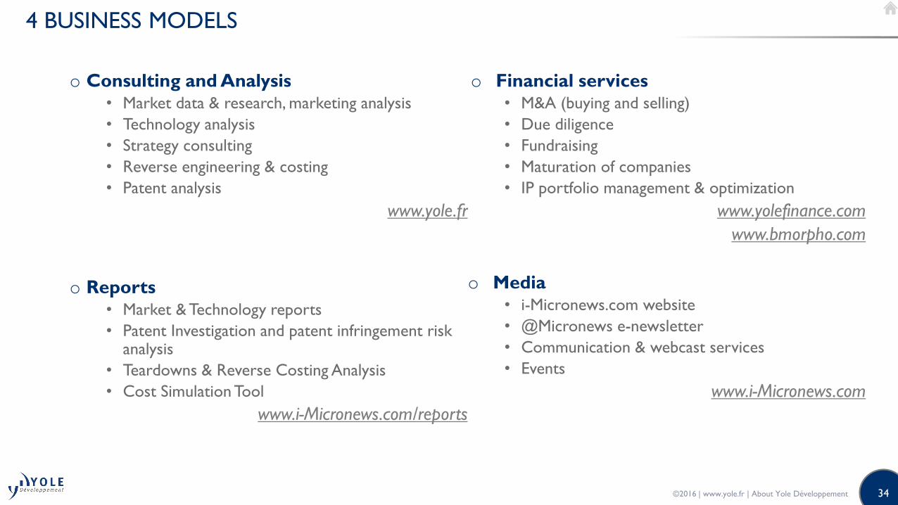
4 BUSINESS MODELS
o Consulting and Analysis
• Market data & research, marketing analysis
• Technology analysis
• Strategy consulting
• Reverse engineering & costing
• Patent analysis
www.yole.fr
o Reports
• Market & Technology reports
• Patent Investigation and patent infringement risk analysis
• Teardowns & Reverse Costing Analysis
• Cost Simulation Tool
www.i-Micronews.com/reports
o Financial services
• M&A (buying and selling)
• Due diligence
• Fundraising
• Maturation of companies
• IP portfolio management & optimization
www.yolefinance.com
www.bmorpho.com
o Media
• i-Micronews.com website
• @Micronews e-newsletter
• Communication & webcast services
• Events
www.i-Micronews.com
©2016 | www.yole.fr | About Yole Développement

35
A GROUP OF COMPANIES
Market,
technology and
strategy
consulting
www.yole.fr
M&A operations
Due diligences
www.yolefinance.com
Innovation and business maker
www.bmorpho.com
Manufacturing costs analysis
Teardown and reverse engineering
Cost simulation tools
www.systemplus.fr
IP analysis
Patent assessment
www.knowmade.fr
©2016 | www.yole.fr | About Yole Développement

36
OUR 2016 REPORTS PLANNING (1/2)
MARKET AND TECHNOLOGY REPORTS
by Yole Développement
o MEMS & SENSORS
− Gas Sensor Technology and Market 2016
− Status of the MEMS Industry 2016
− Sensors for Cellphones and Tablets 2016
− Inkjet Printhead Market & Technology Trends 2016
− Sensors for Biometry and Recognition 2016
− Finger Print Sensors Market and Technologies 2016
− Silicon Photonics 2016
− Emerging Non Volatile Memories 2016
o IMAGING & OPTOELECTRONICS
− Status of the CMOS Image Sensor Industry 2016
− Uncooled Infrared Imaging Technology & Market Trends 2016
− Imaging Technologies for Automotive 2016
− Sensors for Drones & Robots: Market Opportunities and Technology
Evolution 2016
− Silicon Photonics 2016
o MEDTECH
− BioMEMS: Microsystems for Healthcare Applications 2016
− Point of Need Testing 2016: Application of Microfluidic Technologies
o ADVANCED PACKAGING
− Fan-Out WLP: Technology Trends and Business Update 2016
− Embedded Die Packaging: Technologies and Markets Trends 2016
− 2.5D & 3D IC Business Update 2016
− Status and Prospects for the Advanced Packaging Industry in China 2016
− Fan-in Wafer Level Packaging: Market and Technology Trends 2016
o MANUFACTURING
− Equipment and Materials for Fan Out Technology (Wafer vs Panel)**
− Equipment and Materials for 3D T(X)V Technology**
− Thinning & Dicing Equipment for Advanced Packaging, MEMS, Photovoltaics,
LED, CMOS 2016
**To be confirmed
©2016 | www.yole.fr | About Yole Développement

37
OUR 2016 REPORTS PLANNING (2/2)
o COMPOUND SEMICONDUCTORS
− Power SiC 2016: Materials, Devices, Modules, and Applications
− GaN Modules, Devices and Substrates for Power Electronics 2016
− Sapphire Applications & Market 2016: from LED to Consumer Electronics
− GaN RF Devices Market: Applications, Players, Technology, and Substrates
2016 – 2022
− RF components and modules for cellphones 2016**
o LED
− Sapphire Applications and Market 2016: From LED to Consumer Electronics
− Thermal Management for LED and Power 2016
− LED Packaging 2016
− Microdisplays and MicroLEDs 2016**
− UV LEDs - Technology, Manufacturing and Application Trends
− OLED for Lighting - Technology, Industry and Market Trends 2016
− Automotive Lighting: Technologies, Industry and Market Trends 2016
o POWER ELECTRONICS
− Power Electronics for EV/HEV 2016: Market, Innovations and Trends
− Status of Power Electronics Industry 2016
− Passive Components Technologies and Market Trends for Power Electronics
2016
− Power SiC 2016: Materials, Devices, Modules, and Applications
− GaN Modules, Devices and Substrates for Power Electronics 2016
− Inverter Technologies Trends & Market Expectations 2016
− Opportunities for Power Electronics in Renewable Electricity Generation
2016
− Thermal Management for LED and Power 2016
− GaN RF Devices Market: Applications, Players, Technology, and Substrates
2016 - 2022
o BATTERY
− Stationary Storage and Automotive Li-ion Battery Packs
− Beyond Li-ion Batteries: Present and Future Li-ion Technology Challengers
PATENT ANALYSIS by Knowmadeo Patent Infringement (crossed analysis based on Knowmade and System Plus
Analysis expertise)
o Patent Investigation (crossed analysis based on Knowmade & Yole Développement
expertise)
o Patent Landscape
TEARDOWN & REVERSE COSTING by System Plus
ConsultingMore than 30 teardowns and reverse costing analysis and cost simulation tools to be
published in 2016.
©2016 | www.yole.fr | About Yole Développement

38
OUR 2015 PUBLISHED REPORTS LIST
o MEMS & SENSORS
− Sensors and Data Management for Autonomous Vehicles
− Sensors for Wearable Electronics And Mobile Healthcare
− Status of the MEMS Industry
− Uncooled Infrared Imaging Technology & Market Trends
− Infrared Detector Technology & Market Trends
− High-End Gyroscopes, Accelerometers and IMUs for Defense, Aerospace &
Industrial
− Emerging Non Volatile Memory (NVM) Technology & Market Trends
o IMAGING & OPTOELECTRONICS
− Camera Module Industry
− Uncooled Infrared Imaging Technology & Market Trends
− Status of the CMOS Image Sensors
− Infrared Detector Technology & Market Trends
o MEDTECH
− Sample Preparation Automation Through Emerging Microfluidic Technologies
− 2015 Microfluidic Applications in the Pharmaceutical, Life Sciences, In-Vitro
Diagnostic, and Medical Device Markets
− Sensors for Wearable Electronics And Mobile Healthcare
o COMPOUND SEMICONDUCTORS
− Sapphire Applications & Market 2015: from LED to Consumer Electronics
− SiC, GaN, and other Wide Band Gap (WBG) materials for power electronics
applications
− GaN and SiC Devices for Power Electronics Applications
o LED
− LED Lighting Module Technology, Industry and Market Trends 2015
− UV LED - Technology, Manufacturing and Application Trends
− Phosphors & Quantum Dots 2015: LED Downconverters for Lighting & Displays
− Sapphire Applications & Market 2015: from LED to Consumer Electronics
o POWER ELECTRONICS
− Power Packaging Technology Trends and Market Expectations
− Energy Management for Smart Grid, Cities and Buildings: Opportunities for Battery
Electricity Storage Solutions
− Status of Chinese Power Electronics Industry
− New Technologies and Architectures for Efficient Data Center
− IGBT Market and Technology Trends
− Status of Power Electronics Industry
− SiC, GaN, and other Wide Band Gap (WBG) materials for power electronics
applications
− GaN and SiC Devices for Power Electronics Applications
o ADVANCED PACKAGING
− Status of the Advanced Packaging Industry
− Supply Chain Readiness for Panel Manufacturing in Packaging
− Fan-in Wafer Level Packaging: Market and Technology Trends
− Flip Chip: Technologies and Markets Trends
− Fan-Out and Embedded Die: Technologies & Market Trends
o MANUFACTURING
− Photolithography Equipment and Materials for Advanced Packaging, MEMS and
LED Applications
− Emerging Non Volatile Memory (NVM) Technology & Market Trends
©2016 | www.yole.fr | About Yole Développement

39
CONTACT INFORMATION
Follow us on
• Consulting and Specific Analysis
• North America: Steve LaFerriere, Director of Northern America Business DevelopmentEmail: [email protected]
• Japan & Asia: Takashi Onozawa, Representative Director, Yole KKEmail: [email protected]
• RoW: Jean-Christophe Eloy, CEO & President, Yole DéveloppementEmail [email protected]
• Report business
• North America: Steve LaFerriere, Director of Northern America Business DevelopmentEmail: [email protected]
• Europe: Lizzie Levenez, EMEA Business Development ManagerEmail: [email protected]
• Japan & Asia: Takashi Onozawa, Representative Director, Yole KK.Email: [email protected]
• Greater China: Mavis Wang, Business Development DirectorEmail: [email protected]
• Financial services
• Jean-Christophe Eloy, CEO & PresidentEmail: [email protected]
• General
• Email: [email protected]
©2016 | www.yole.fr | About Yole Développement