lectures on memory interface on memory interface. ... • the memory system is divided into three...
TRANSCRIPT
Designed and Presented by
Dr. Ayman Elshenawy Elsefy
Dept. of Systems & Computer Eng..
Al-Azhar University
Email : [email protected]
eaymanelshenawy.wordpress.com
Lectures on Memory Interface

Lecture 1Microprocessor and Memory

Microprocessor Based Computer Systems
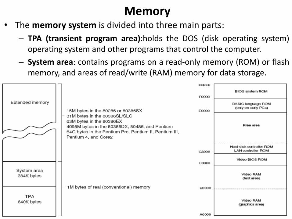
Memory• The memory system is divided into three main parts:
– TPA (transient program area):holds the DOS (disk operating system)operating system and other programs that control the computer.
– System area: contains programs on a read-only memory (ROM) or flashmemory, and areas of read/write (RAM) memory for data storage.
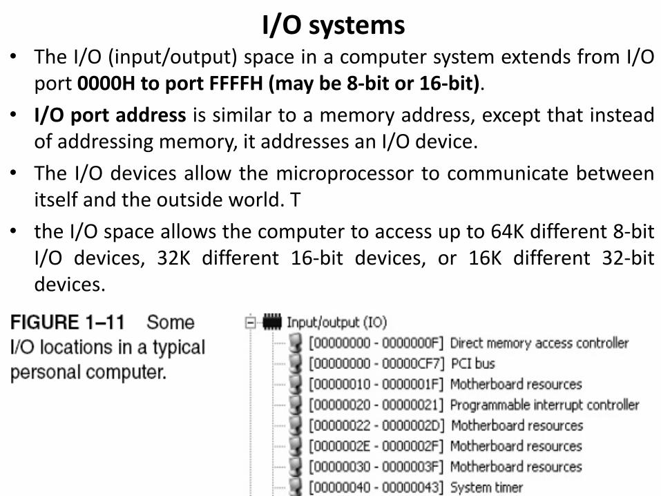
I/O systems• The I/O (input/output) space in a computer system extends from I/O
port 0000H to port FFFFH (may be 8-bit or 16-bit).
• I/O port address is similar to a memory address, except that insteadof addressing memory, it addresses an I/O device.
• The I/O devices allow the microprocessor to communicate betweenitself and the outside world. T
• the I/O space allows the computer to access up to 64K different 8-bitI/O devices, 32K different 16-bit devices, or 16K different 32-bitdevices.

Busses• A bus is a common group of wires that interconnect components in a
computer system.
• The buses transfer address, data, and control information between the microprocessor and its memory and I/O systems.
• Three buses exist for this transfer of information:
– Address
– Data Bus,
– Control signals Bus.

Microprocessor CPU• Is the controlling element in a computer system.
• controls memory and I/O through a series of connections called buses.
• The buses select an I/O or memory device, transfer data between an I/O device or memory and the CPU, and control the I/O and memory system.
• Memory and I/O are controlled through instructions that are stored in the memory and executed by the CPU.
• The CPU performs three main tasks:
– data transfer between itself and the memory or I/O systems.
– simple arithmetic and logic operations
– program flow via simple decisions.
• The power of the CPU is in its capability to execute billions of millions of instructions per second from a program or software (group of instructions) stored in the memory system.

Microprocessor

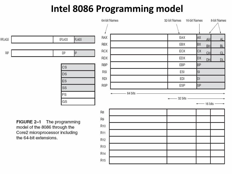
Intel 8086 Programming model• The programming model of the 8086 through the Core2 is considered
to be program visible (registers are used during applicationprogramming and are specified by the instructions).
• Some registers, detailed later in this chapter, are considered to beprogram invisible ( are not addressable directly during applicationsprogramming) but may be used indirectly during systemprogramming.
• Only the 80286 and above contain the program-invisible registersused to control and operate the protected memory system and otherfeatures of the microprocessor.
Intel 8086 Programming model
Intel 8086 Programming model• The programming model contains 8, 16, and 32-bit registers. And
some contains 64-bit registers when operated in the 64-bit mode
• The 8-bit registers are AH, AL, BH, BL, CH, CL, DH, and DL and arereferred using two-letter designations (ADD AL,AH instruction addsthe 8-bit contents of AH to AL, only AL changes due to instruction.)
• The 16-bit registers are AX, BX, CX, DX, SP, BP, DI, SI, IP, FLAGS, CS, DS,ES, SS, FS, and GS. Some of them consists of tow 8-bit registers(AX=AH + AL).
• The 16-bit registers are referenced with the two-letter designationssuch as AX ( ADD DX, CX instruction adds the 16-bit contents of CX toDX, Only DX changes due to this instruction).
• The extended 32-bit registers are EAX, EBX, ECX, EDX, ESP, EBP, EDI,ESI, EIP, and EFLAGS. These 32-bit extended registers, and 16-bitregisters FS and GS( ADD ECX, EBX adds the 32-bit contents of EBX toECX , Only ECX changes due to this instruction).

Intel 8086 Programming model• General-purpose registers:
– include EAX, EBX, ECX, EDX, EBP, EDI, and ESI.
– Hold various data sizes (bytes, words, or double words) and are used for almost any purpose, as dictated by a program.
– RAX (accumulator) , RBX (base index) ,
• Special Purpose registers
– include RIP, RSP, and RFLAGS; and the segment registers include CS, DS, ES, SS, FS, and GS.
– RIP (instruction register) , RSP (Stack pointer) ,RFLAGS (indicate the condition of the microprocessor and control its operation such as (C carry), (P parity ), (Z zero), (S Sign), (I interrupt), (O Overflow),…...
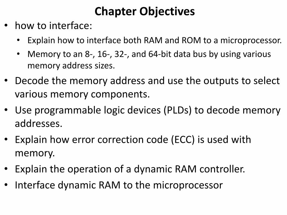
Chapter Objectives• how to interface:
• Explain how to interface both RAM and ROM to a microprocessor.
• Memory to an 8-, 16-, 32-, and 64-bit data bus by using various memory address sizes.
• Decode the memory address and use the outputs to select various memory components.
• Use programmable logic devices (PLDs) to decode memory addresses.
• Explain how error correction code (ECC) is used with memory.
• Explain the operation of a dynamic RAM controller.
• Interface dynamic RAM to the microprocessor

Introduction• Every microprocessor-based system has a memory system.
• There are two main types of memory:
• Read-Only memory (ROM). contains system software
and permanent system data.
• Random Access Memory (RAM) or read/write
memory, contains temporary data and application
software.
• This allows virtually any microprocessor to be interfaced to any
memory system.
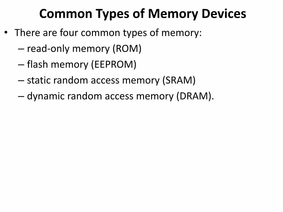
Common Types of Memory Devices
• There are four common types of memory:
– read-only memory (ROM)
– flash memory (EEPROM)
– static random access memory (SRAM)
– dynamic random access memory (DRAM).

• Computers employ many different types of memory to hold
data and programs.
Semi-conductor Memories
magnetic disks, USB sticks, DVDs etc.)
• Each type has its own characteristics and uses.
Computer Memory

• For the same price:
• CPU processing speed (the number of
instructions executed per second) has doubled
every 18 months.
• Computer memory has quadrupling in size every
36 months.
• Memory speed, has increased at a rate of less than
10% per year.
• A gap between the speed of the processor and the
speed of memory also increases.
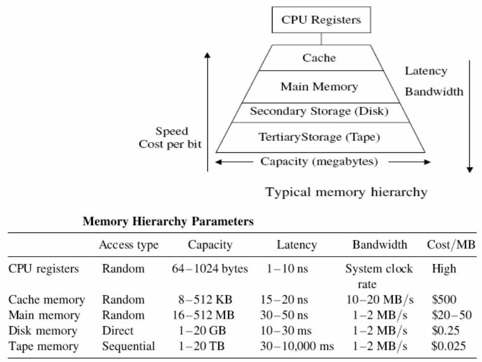
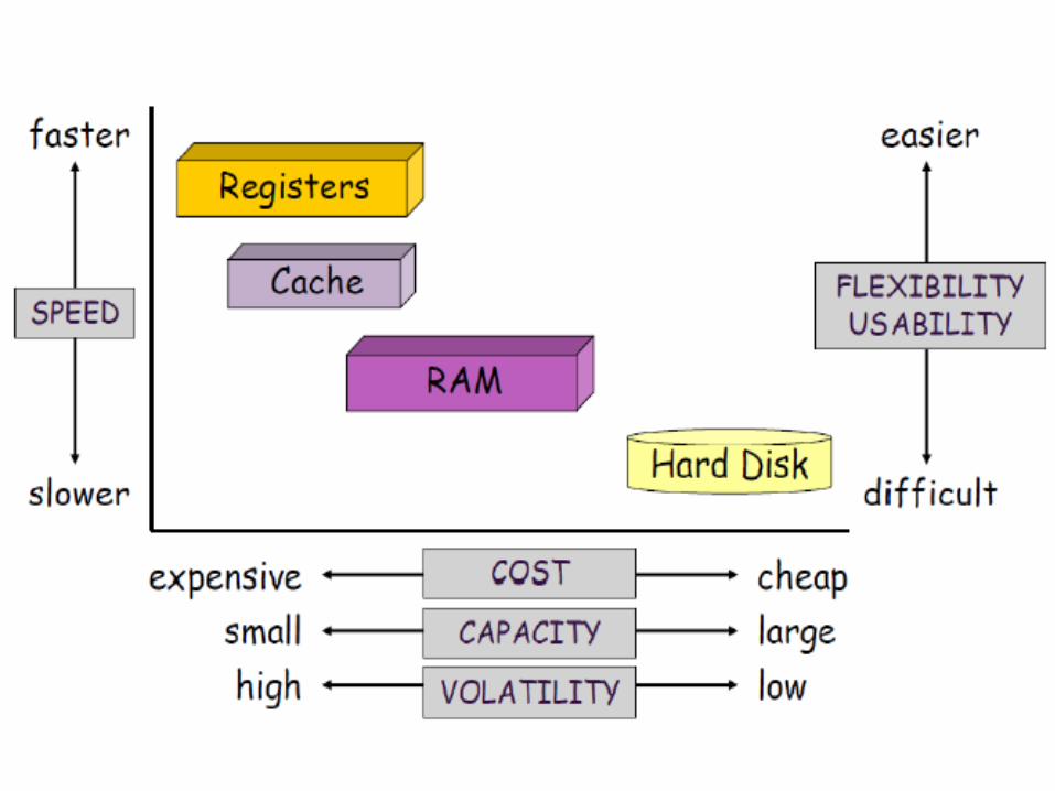
Memory Hierarchy

• A computer have several types of memory, ranging from
fast, expensive internal registers, to slow, inexpensive
Hard Magnetic Disks.
• Registers:• are matched in speed to the CPU
• consume a significant amount of power.
• only a small number of registers in a processor
• more expensive.
• Secondary storage:• such as hard magnetic disks.
• the cost per stored bit is small in terms of money and electrical
power.
• Access time is very long when compared with registers.
• Between the registers and secondary storage there are a
number of other forms of memory that bridge the gap
between the two.
Memory Hierarchy
• The memory hierarchy can be characterized by a number of
parameters:
• Access Type: how physically the memory read/write is
done (Random or Sequential).
• Capacity measured in bytes or KB or MB.
• Cycle time: the time elapsed from the start of a read
operation to the start of a next read.
• Latency is defined as the time interval between the
request for information and the access to the first bit of
that information.
• Bandwidth: the number of bits that can be accessed in
one second.
• Cost of a memory is usually specified as dollars/MB
• Total Cost = cost/MB * Memory Size.
Memory Hierarchy
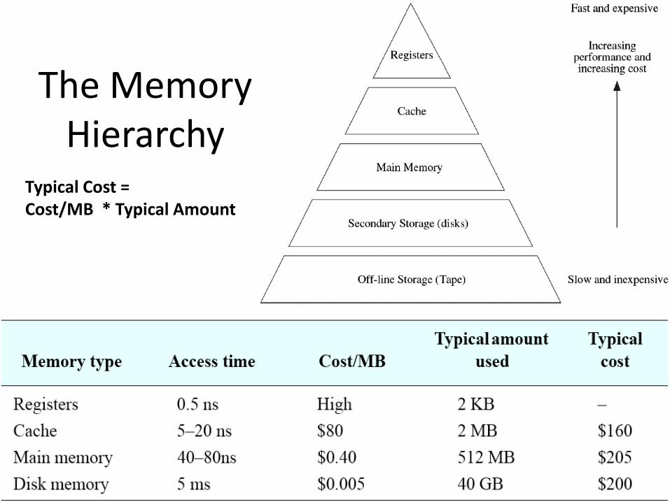
The Memory Hierarchy
Typical Cost = Cost/MB * Typical Amount

Memory Hierarchy
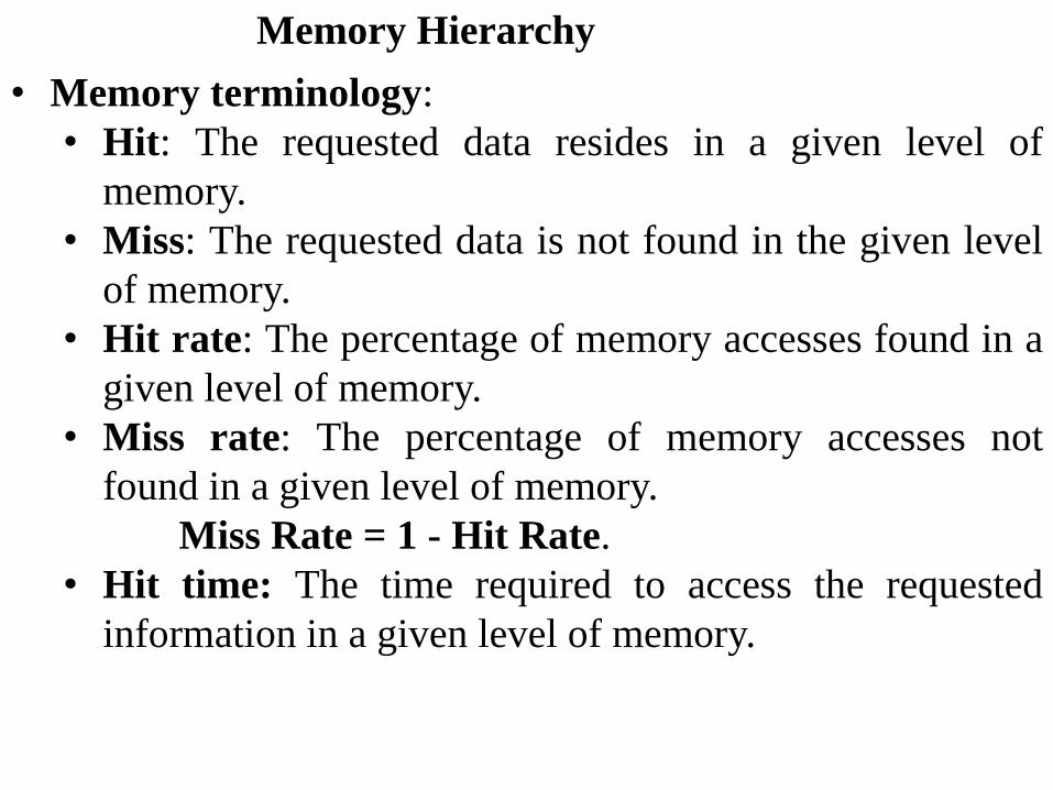
• Memory terminology:
• Hit: The requested data resides in a given level of
memory.
• Miss: The requested data is not found in the given level
of memory.
• Hit rate: The percentage of memory accesses found in a
given level of memory.
• Miss rate: The percentage of memory accesses not
found in a given level of memory.
Miss Rate = 1 - Hit Rate.
• Hit time: The time required to access the requested
information in a given level of memory.
Memory Hierarchy
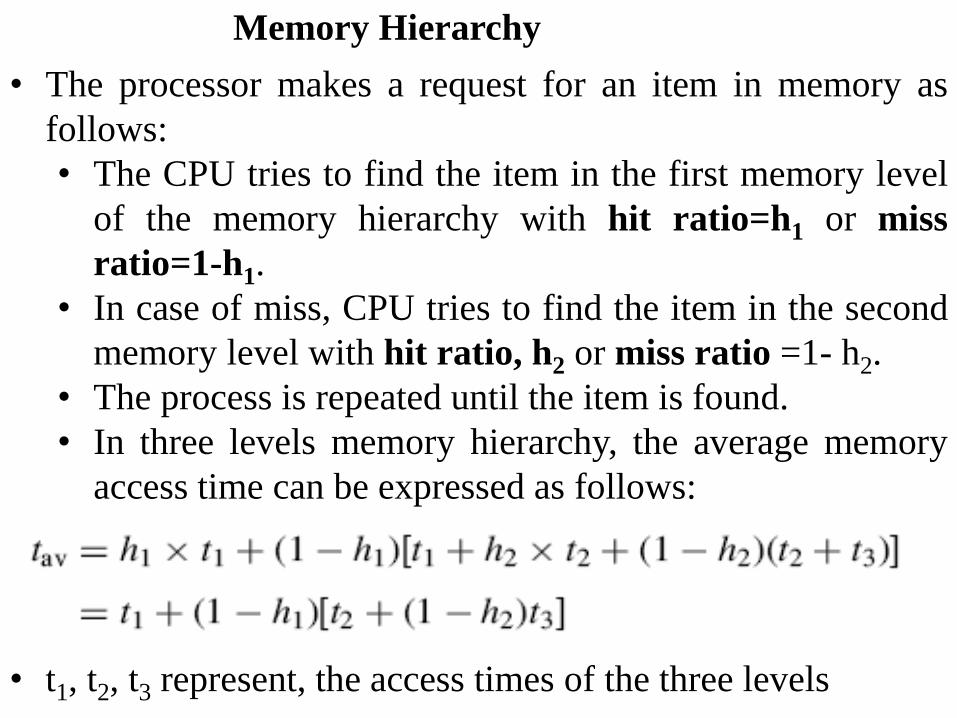
• The processor makes a request for an item in memory as
follows:
• The CPU tries to find the item in the first memory level
of the memory hierarchy with hit ratio=h1 or miss
ratio=1-h1.
• In case of miss, CPU tries to find the item in the second
memory level with hit ratio, h2 or miss ratio =1- h2.
• The process is repeated until the item is found.
• In three levels memory hierarchy, the average memory
access time can be expressed as follows:
• t1, t2, t3 represent, the access times of the three levels

Main Memory
• The Figure shows an interface between the main memory
and the CPU using two CPU registers:• MAR (Memory Address Register): used to store the address of
specific location.
• MDR (Memory Data Register): used to hold the data to be stored
and/or retrieved in/from the memory location

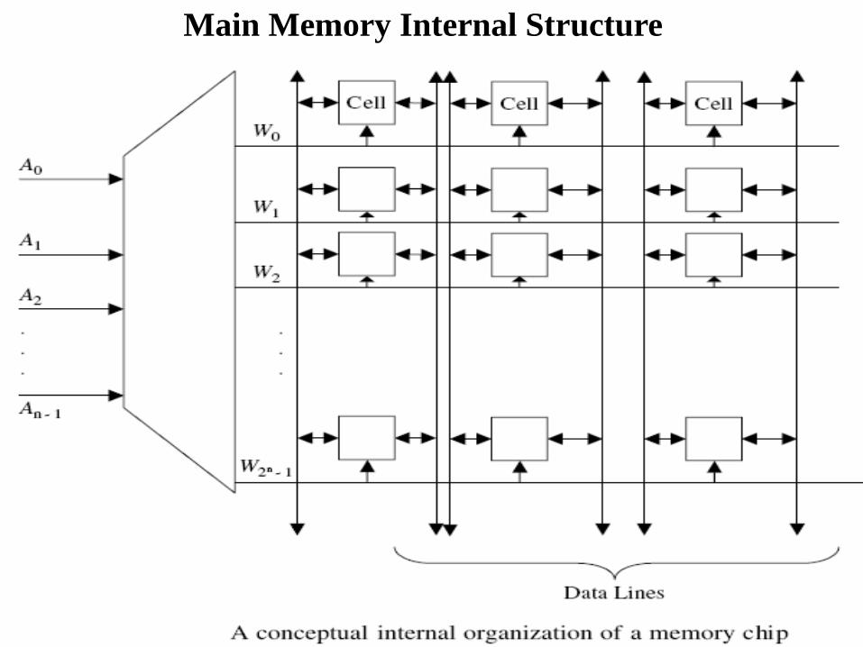
Main Memory Internal Structure
• Main memory consists of:
• rows and columns of basic cells that store one bit of
information.
• Cells in one row can be used to form a memory word.
• Address lines An-1An-2 . . A1A0 are used as inputs to the
address decoder in order to generate the word select lines
W2n-1 . . .W1W0.
• A given word select line is common to all memory cells
in the same row and is used to enable all cells in a row
for read or write.
• Data (bit) lines are used to input or output the contents
of cells. Each memory cell is connected to two data
lines. A given data line is common to all cells in a given
column.

2-1/2D Organization of a 64-Word by One-Bit RAM
Main Memory Internal Structure

Memory Pin connections
• All Memory devices have the following pins:
– Address input Pins
– Data input/output Pins
– Selection input Pins
– Control input Pins

Address Connections
• Used to select a memory location within the device.
• Labeled from A0 (least significant address input), to An-1
where n can be any value.
• No. of address pins = Log2 (Memory Locations)
• No. of Memory Locations = 2(Address Pins)
• A 1K memory device has 1024 memory locations and 10
address pins.
• It takes a 10-bit binary number to select any single
location on a 1024-location device.
• 1024 different combinations
• if a device has 11 address connections, it
has 211 =2048 bit = 2KB internal memory locations

Address Input Pins
• The number 400H (0100 0000 0000)B represents a
1K-byte section of the memory system.
• If a memory device is decoded to begin at memory
address 10000H and it is a 1K device, its last location
is at address (10000H + 400H)-1H = 103FFH—one
location less than 400H.
• 1000H is 4K. A memory device that contains a starting
address of 14000H that is 4K bytes long ends at
location 14FFFH—one location less than 1000H.
• A third number is 64K, or 10000H. A memory that
starts at location 30000H and ends at location 3FFFFH
is a 64K-byte memory.

• All memory devices have a set of data outputs or
input/outputs (bidirectional common I/O pins).
• data connections are points at which data are entered for
storage (WRITE) or extracted for reading
• Data pins are labeled D0 through D7 for an 8-bit-wide
memory device ( byte-wide memory ). most devices are 8
bits wide, some are 16 bits, 4 bits, or just 1 bit wide
• A memory device with 1K memory locations and 8 bits in
each location is often listed as a 1K 8 by the manufacturer
• Memory devices are often classified according to total bit
capacity.
Data Connections

• Each memory device has an input that selects or enables the
memory device ( sometimes more than one)
• This type of input is most often called a Chip Select (CS)
Chip Enable (CE) or simply Select (S) input.
• RAM memory generally has at least one or tow inputs, and
ROM has at least one
• If more than one CE connection is present,
all must be activated to read or write data.
Selection Connections

• ROM usually has one control input OE (Output Enable)
• allows data flow from output data pins.
• The OE enables and disables a set of three-state buffers located in
the device and must be active to read data.
• RAM has either one or two control inputs:
• if one control input, it is often called R/W (Read / Write)
• If the RAM has two control inputs:
– WE write enable must be active to perform memory write.
– OE Output Enable must be active to perform a memory read
• when the two controls are present, they must never both be active
at the same time
• If both inputs are inactive, data are neither written nor read. the
connections are at their high-impedance state.
Control Connections
Main Memory Cell
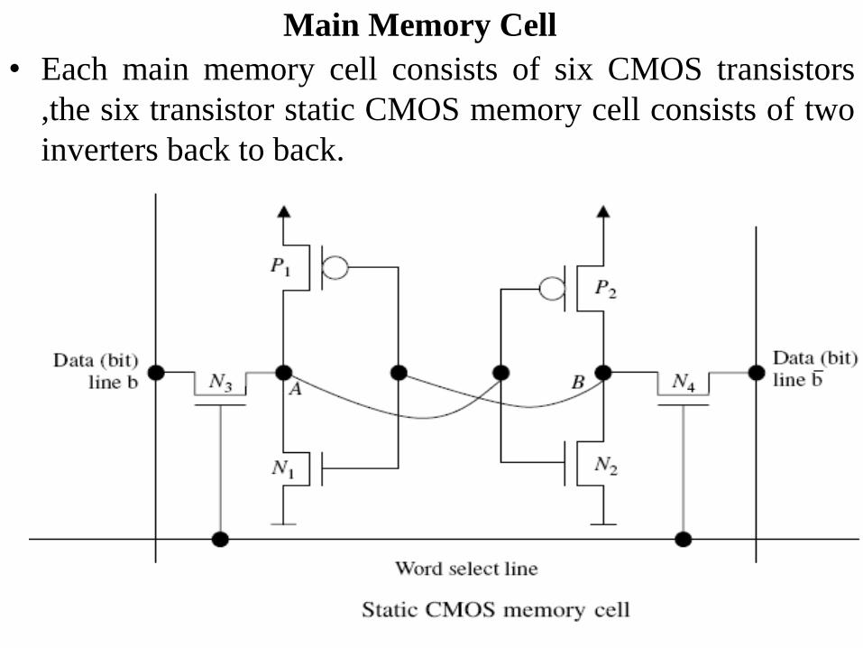
• Each main memory cell consists of six CMOS transistors
,the six transistor static CMOS memory cell consists of two
inverters back to back.
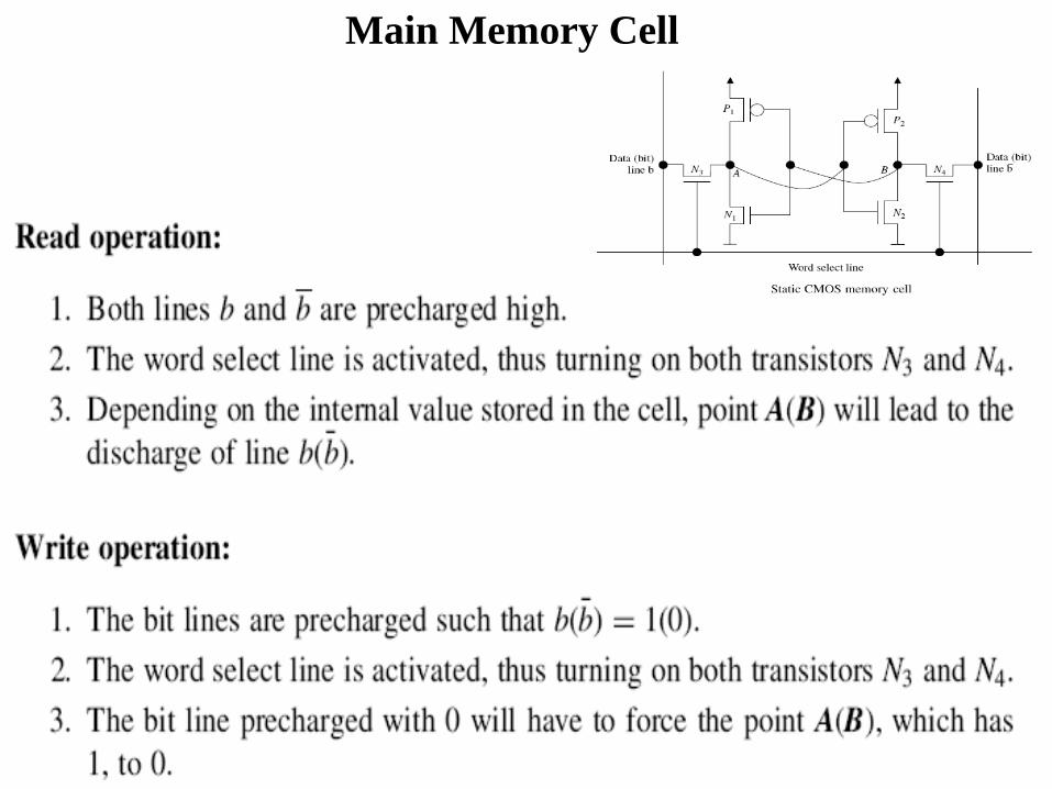
Main Memory Cell
Memory Design
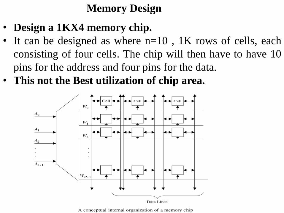
• Design a 1KX4 memory chip.
• It can be designed as where n=10 , 1K rows of cells, each
consisting of four cells. The chip will then have to have 10
pins for the address and four pins for the data.
• This not the Best utilization of chip area.

• Design a 1KX4
memory chip.
• It can be designed as
64 rows, each
consisting of 64 cells.
In this case, 6 address
lines forming the row
address.
• The remaining 4
address lines (column
address) will be used
to select the
appropriate 4 bits
among the available
64 bits constituting a
row.
Memory Design Factors
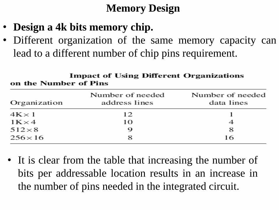
• Design a 4k bits memory chip.
• Different organization of the same memory capacity can
lead to a different number of chip pins requirement.
Memory Design
• It is clear from the table that increasing the number of
bits per addressable location results in an increase in
the number of pins needed in the integrated circuit.
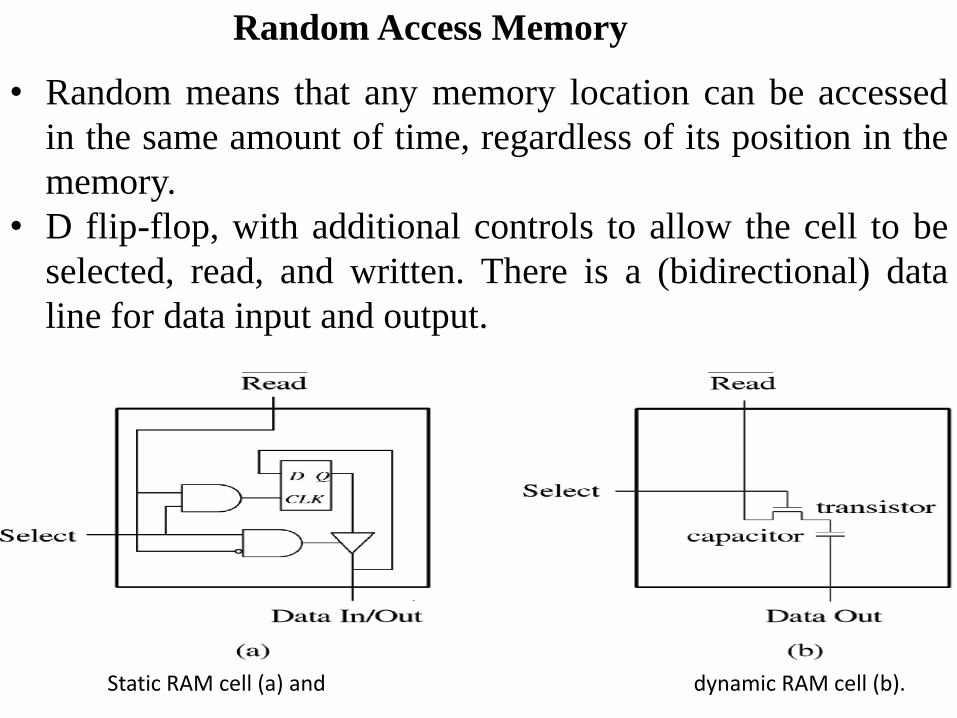
• Random means that any memory location can be accessed
in the same amount of time, regardless of its position in the
memory.
• D flip-flop, with additional controls to allow the cell to be
selected, read, and written. There is a (bidirectional) data
line for data input and output.
Random Access Memory
Static RAM cell (a) and dynamic RAM cell (b).

• A Four-Word Memory with Four Bits per Word in a 2D Organization.
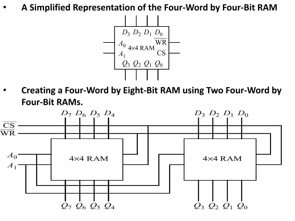
• A Simplified Representation of the Four-Word by Four-Bit RAM
• Creating a Four-Word by Eight-Bit RAM using Two Four-Word by Four-Bit RAMs.

Two Four-Word by Four-Bit RAMs Make up an Eight-Word by Four-Bit RAM

ROM Memory• The read-only memory (ROM):
– permanently stores programs and data that are resident to thesystem and must not change when power supply isdisconnected. The ROM is permanently programmed
– non-volatile memory, because its contents do not change even if power is disconnected.
• Today, the ROM is available in many forms.
• A device we call a ROM is purchased in mass quantitiesfrom a manufacturer and programmed during itsfabrication at the factory.

ROM Memory (EPROM and PROM)• The EPROM (erasable programmable read-only memory),
a type of ROM, is more commonly used when softwaremust be changed often or when too few are in demand tomake the ROM economical.
• An EPROM is programmed in the field on a device calledan EPROM programmer. The EPROM is also erasable ifexposed to high-intensity ultraviolet light for about 20minutes or so, depending on the type of EPROM.
• The PROM (programmable read-only memory) is alsoprogrammed in the field by burning open tiny NI-chromeor silicon oxide fuses; but once it is programmed, it cannotbe erased.

ROM Memory (Flash Memory)• The flash memory is also often called an EEPROM
(electrically erasable programmable ROM),or a NOVRAM (non-volatile RAM).
– Are electrically erasable in the system, but they require more time to erase than a normal RAM.
– The flash memory device is used to store setup information for systems such as the video card in the computer.
– It has all but replaced the EPROM in most computer systems for the BIOS memory.
– Some systems contain a password stored in the flash memory device.
– Flash memory has its biggest impact in memory cards for digital cameras and memory in MP3 audio players.

ROM Memory (Flash Memory)
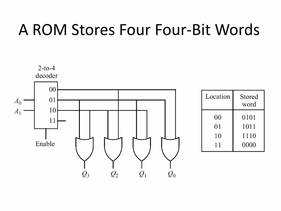
A ROM Stores Four Four-Bit Words
ROM Memory (Flash Memory)• Data appear on the output connections only after a logic 0
is placed on both 𝐶𝐸 and 𝑂𝐸 pin connections.
• If 𝐶𝐸 and 𝑂𝐸 are not both logic 0s, the data output connections remain at their high-impedance or off states.
• Note that the VPP pin must be placed at a logic 1 level for data to be read from the EPROM.
• In some cases, the VPP pin is in the same position as the 𝑊𝐸 pin on the SRAM.
• This will allow a single socket to hold either an EPROM or an SRAM.

ROM Memory (Flash Memory)

ROM Memory (Flash Memory)
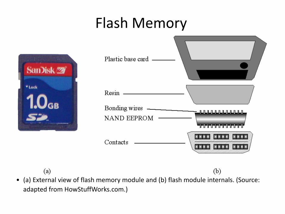
Flash Memory
• (a) External view of flash memory module and (b) flash module internals. (Source:
adapted from HowStuffWorks.com.)

Memory Access Time• Memory access time TACC—the time that it takes the
memory to read information. TACC is measured from theappearance of the address at the address inputs until theappearance of the data at the output connections.
• This is based on the assumption that the 𝐶𝐸 input goes low at the same time that the address inputs become stable. Also, 𝑂𝐸 must be a logic 0 for the output connections to become active.
• The basic speed of EPROM is 450 ns. And 086/8088 operated with a 5 MHz clock allowed memory 460 ns to access data.
• Wait states are required to operate properly with the 8086/8088 microprocessors.

Static RAM Devices• is a RAM chips that are based upon flip-flops, because the
contents of each location persist as long as power is
applied to the chips.
• Static RAM memory devices retain data for as long as DC
power is applied. Because no special action (except power)
is required to retain stored data, these devices are called
static memory.
• They are also called volatile memory because they will not
retain data without power.
• The SRAM, which stores temporary data, is used when the
size of the read/write memory is relatively small.

Static RAM Devices

Static RAM Devices

Static RAM Devices

Static RAM Devices

Static RAM Devices

Dynamic RAM Devices DRAM• The same as SRAM, except that it retains data for only 2 or
4 ms on an integrated capacitor. After 2 or 4 ms, thecontents of the DRAM must be completely rewritten(refreshed) because the capacitors, which store a logic 1 orlogic 0, lose their charges.
• Refresh is reading the content of memory location and write it again which is impossible task. This occurs during write, read or during special refresh cycle.
• the manufacturer has internally constructed the DRAM differently from the SRAM. So that, the entire content of the memory are refreshed with 256 reads in a 2- 4-ms.
• DRAM requires so many address pins that themanufacturers have decided to multiplex the addressinputs.

Dynamic RAM Devices DRAM• Is a RAM chips, employ a capacitor , which stores a
minute amount of electric charge, in which the charge
level represents a 1 or a 0.
• Capacitors are much smaller than flip-flops, so a
capacitor based DRAM can hold much more
information in the same area than an SRAM.
• Since the charges on the capacitors dissipate with time,
the charge in the capacitor storage cells in DRAMs
must be restored, or refreshed frequently.
Dynamic RAM Devices DRAM
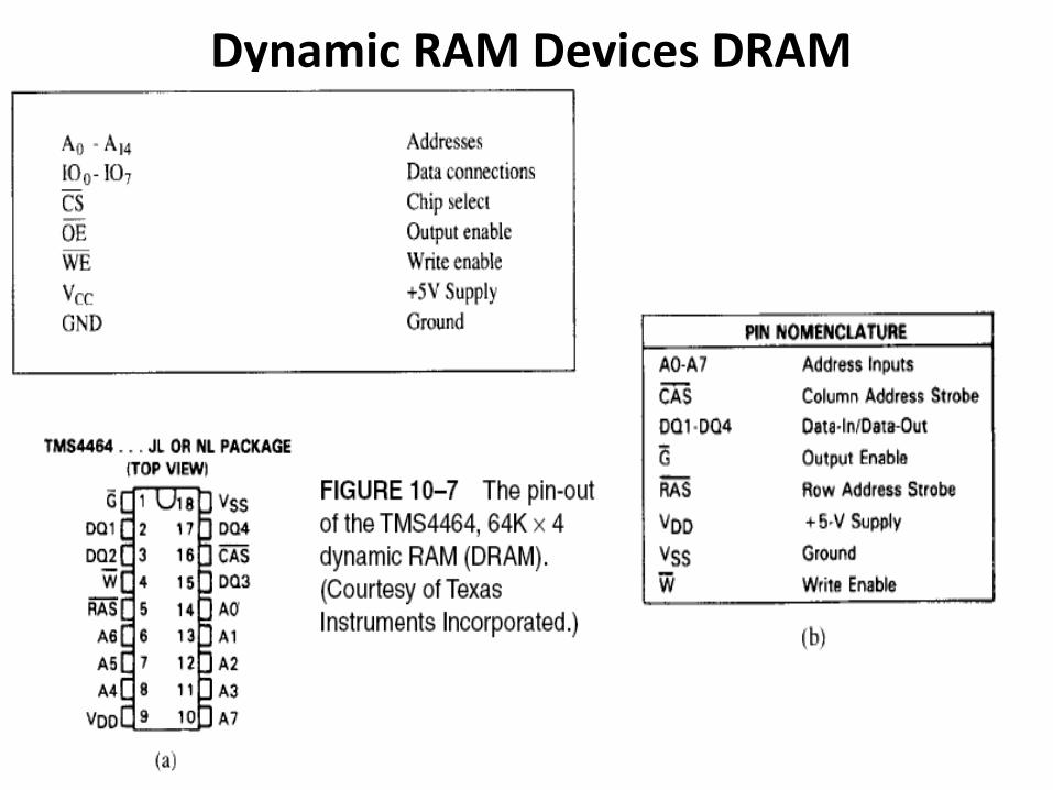
Dynamic RAM Devices DRAM• A DRAM 64K × 4 DRAM, which stores 256K bits of data. Can
use only eight address inputs instead of 16—the number required to address 64K memory locations.
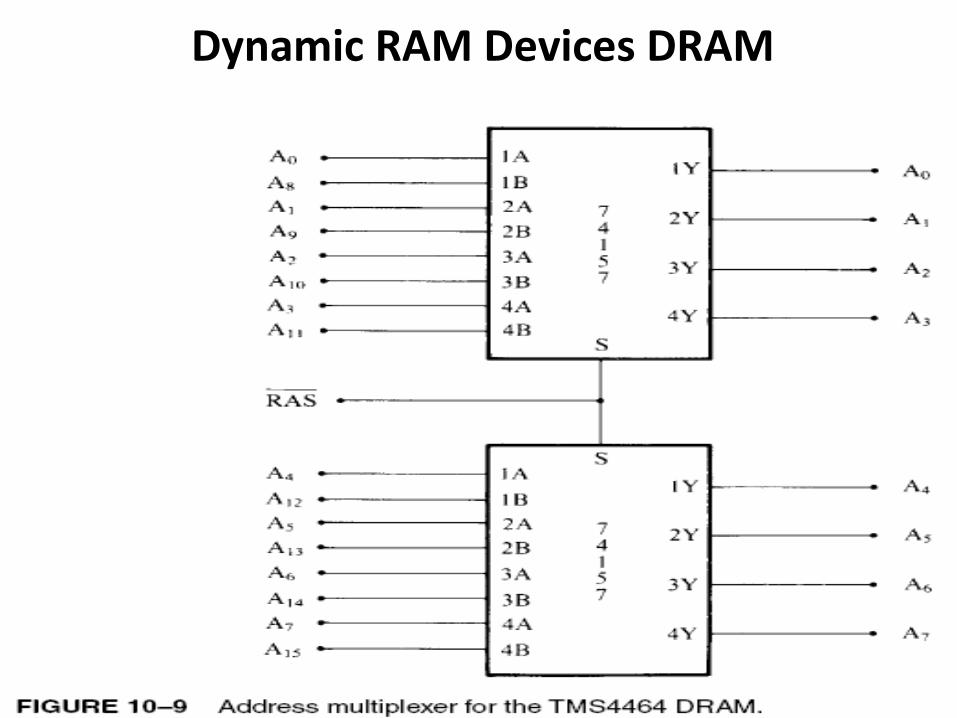
• The Multiplexing operation requires two special pins: the column address strobe (CAS ) and row address strobe ( RAS).
• First, A0–A7 are placed on the address pins and strobedinto an internal row latch by RAS as the row address.
• Next, the address bits A8--A15 are placed on the sameeight address inputs and strobed into an internal columnlatch by CAS as the column address.
• The 16-bit address held in these internal latches addresses the contents of one of the 4-bit memory locations.
Dynamic RAM Devices DRAM

Dynamic RAM Devices DRAM

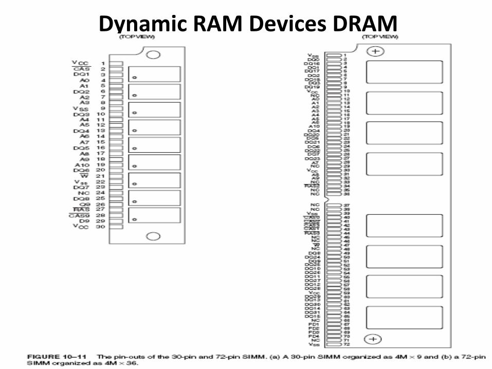
Dynamic RAM Devices DRAM• DRAM memory is often placed on small circuit boards
called SIMMs (Single In-Line Memory Modules).
• The 30-pin SIMM is organized most often as 1M × 8 or 1M × 9, and 4M × 8 or 4M × 9.
• The ninth bit is the parity bit.
• Also shown is a newer 72 pin SIMM. The 72-pin SIMMs are often organized as 1M × 32 or 1M × 36 (with parity).
• Other sizes are 2M × 32, 4M × 32, 8M × 32, and 16M × 32. These are also available with parity.
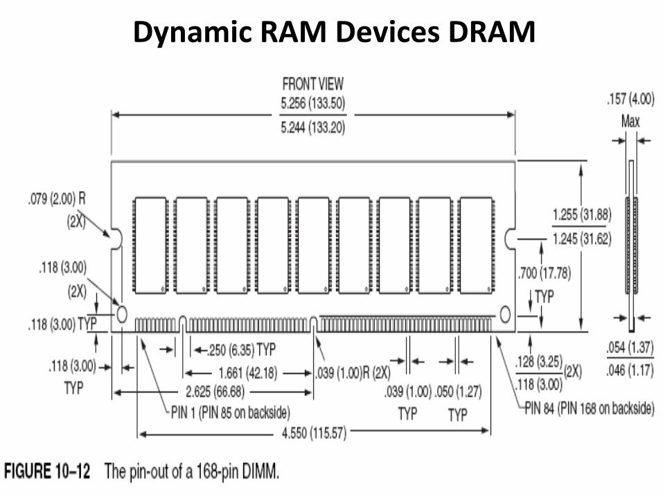
Dynamic RAM Devices DRAM• Pentium 4 microprocessors have a 64-bit wide data bus,
• SIMMs must be used in pairs to obtain a 64-bit-wide data connection.
• Today, the 64-bit-wide DIMMs (Dual In-line Memory Modules) have become the standard in most systems.
• The memory on these modules is organized as 64 bits wide. The common sizes available are 16M bytes (2M ×64), 32M bytes (4M × 64), 64M bytes (8M × 64), 128M bytes (16M × 64), 256M bytes (32M × 64), 512M bytes
• (64M × 64), and 1G bytes (128M × 64).
Dynamic RAM Devices DRAM
Dynamic RAM Devices DRAM

Sheet 11. What types of connections are common to all memory devices?
2. List the number of words found in each memory device for the following numbers of address connections:
(a) 8 (b) 11 (c) 12 (d) 13 (e) 20
3. List the number of data items stored in each of the following memory devices and the number of bits in each datum:
4. (a) 2K × 4 (b) 1K × l (c) 4K × 8 (d) 16K × 1 (e) 64K × 4
5. What is the purpose of the 𝐶𝑆 or 𝐶𝐸 pin on a memory component?
6. What is the purpose of the𝑂𝐸 pin on a memory device?
7. What is the purpose of the 𝑊𝐸 pin on a SRAM?
8. How many bytes of storage do the following EPROM memory devices contain?
(a) 2708 (b) 2716 (c) 2732 (d) 2764 (e) 27512
Sheet 19. Why won’t a 450 ns EPROM work directly with a 5 MHz 8088?
10. What can be stated about the amount of time needed to erase and write a location in a flash memory device?
11. SRAM is an acronym for what type of device?
12. The 4016 memory has a 𝐺 pin, 𝑆 and 𝑊 pin, and a pin. What are these pins used for in this RAM?
13. How much memory access time is required by the slowest 4016?
14. DRAM is an acronym for what type of device?
15. The 256M DIMM has 28 address inputs, yet it is a 256M DRAM. Explain how a 28-bit memory address is forced into 14 address inputs.
16. What are the purposes of the 𝐶𝐴𝑆 and 𝑅𝐴𝑆 inputs of a DRAM?
17. How much time is required to refresh the typical DRAM?