lectures chpter#4 mosfet of sedra semith (micro electronic circuits)
TRANSCRIPT

1
MOS Field-EffectTransistors (MOSFETs)

MOSFET ( Voltage Controlled Current Device)• MOS Metal Oxide Semiconductor
Physical Structure
• FET Field Effect TransistorThe current controlled mechanism is based on an electric field established by the
voltage applied to the control terminal – GATE
• Uni-polar Current is conducted by only one carrier
• IGFET Insulated Gate FET
• CMOSFET Complementary MOSFET
• 1930 was Known, 1960s Commercialized
1970s Most commonly used VLSI
• NMOSFET/PMOSFET n/p-channel enhancement mode MOSFET

MOSFET• Small Size
• Manufacturing process is simple
• Requires comparatively low power
• Implement digital & analog functions with a fewer resistors very large scale Integrated (VLSI) circuit
• Study Includes– Physical structure– Operation– Terminal characteristics– Circuit Models– Basic Circuit application
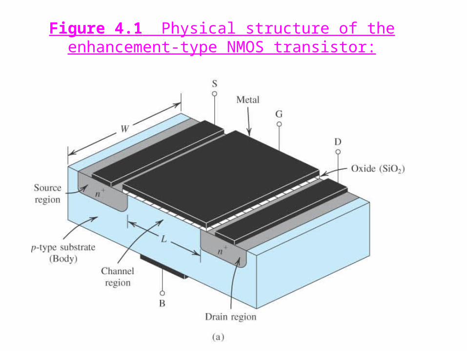
Figure 4.1 Physical structure of the enhancement-type NMOS transistor:

Device Structure• Types “n” channel enhancement MOSFET
“p” channel enhancement MOSFET
• “n” Channel MOSFET– Fabricated on a p-type substance that provides physical support for the
device.
– Two heavily doped n-type region are created • n+ Source (‘S’) n- for lightly doped ‘n’ type silicon• n+ Drain (‘D’) n+ for heavily doped ‘n’ type
silicon
– Area between source & Drain• Thin Layer of Silicon dioxide (SiO2) is grown with thickness of tox =
2-50 nanometers An excellent electrical insulator
• Metal is deposited on top of the oxide layer to form the Gate electrode. Metal contact is made to Source & Drain and the substrate (Body)

Figure 4.1 Physical structure of the enhancement-type NMOS transistor
Cross-section. Typically L = 0.1 to 3 m, W = 0.2 to 100 m, and
the thickness of the oxide layer (tox) is in the range of 2 to 50 nm.
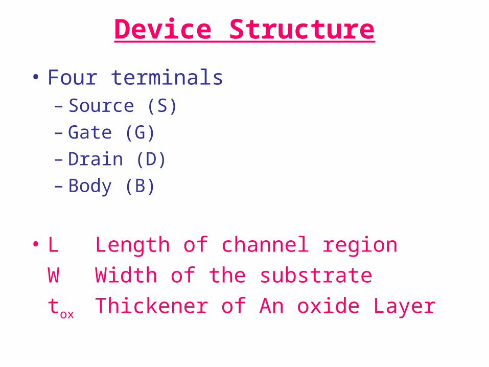
• Four terminals– Source (S)– Gate (G)– Drain (D)– Body (B)
• L Length of channel region
W Width of the substrate
tox Thickener of An oxide Layer
Device Structure
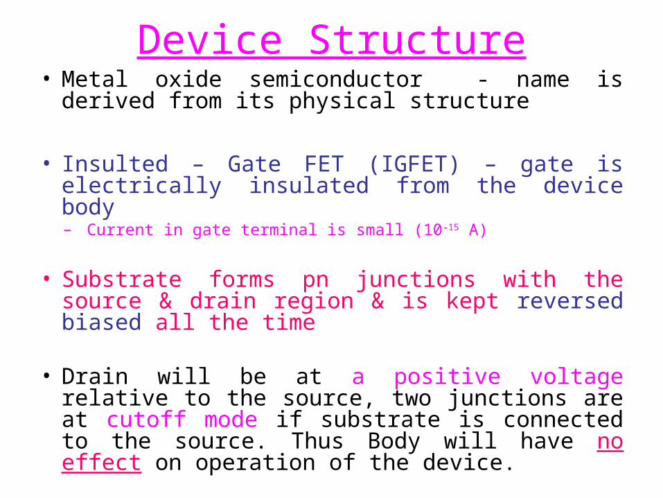
• Metal oxide semiconductor - name is derived from its physical structure
• Insulted – Gate FET (IGFET) – gate is electrically insulated from the device body– Current in gate terminal is small (10-15 A)
• Substrate forms pn junctions with the source & drain region & is kept reversed biased all the time
• Drain will be at a positive voltage relative to the source, two junctions are at cutoff mode if substrate is connected to the source. Thus Body will have no effect on operation of the device.
Device Structure
Principle of operation
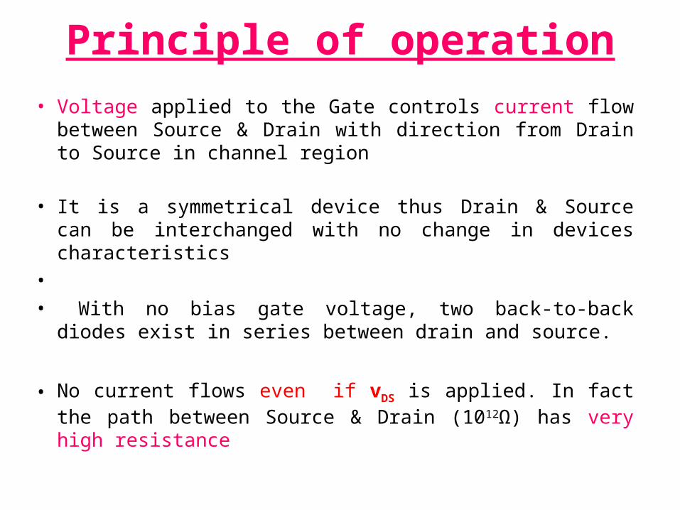
• Voltage applied to the Gate controls current flow between Source & Drain with direction from Drain to Source in channel region
• It is a symmetrical device thus Drain & Source can be interchanged with no change in devices characteristics
• • With no bias gate voltage, two back-to-back diodes exist
in series between drain and source.
• No current flows even if vDS is applied. In fact the path between Source & Drain (1012Ω) has very high resistance
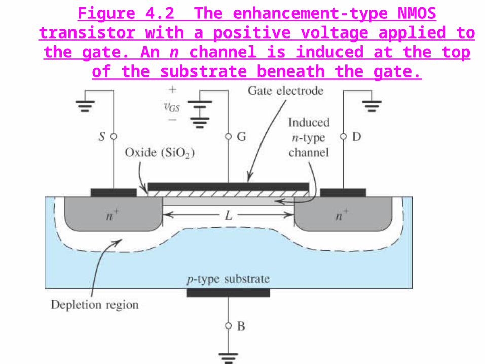
Figure 4.2 The enhancement-type NMOS transistor with a positive voltage applied to the gate. An n channel is induced at the top of the substrate beneath the gate.

Creating a Channel for Current Flow
• Source & Drain are grounded and a positive voltage (vGS) is applied to the gate.
• Holes are repelled-leaving behind a carrier depletion-region.
• Depletion region is populated with the bounded negative charges associated with the acceptor atoms and are uncovered because the neutralizing holes have been push downward into the substrate.
• Positive gate attracts electrons from the n+ source & drain region into the channel region.
• Due to electrons accumulated under the gate, an ‘n’ region is created & connects source & drain region.
• Thus if voltage is applied between source & drain, current flows due to mobile electrons between drain & source.
• ‘n’ region forms a channel – ‘n’ channel MOSET (NMOSFET)
Channel for Current Flow

• An ‘n’ channel MOSFET is formed in a ‘p’ type substrate. Known as “Inversion Layer”.
• The value of vGS that causes sufficient number of mobile electrons to be accumulate in the channel region to form conducting channel is called threshold Voltage “Vt”.
• Vt for ‘n’ channel is positive & value is 0.5 to 1V
Channel for Current Flow

Channel for Current Flow
• Gate & channel region form a parallel plate capacitor, with oxide layer as the capacitor dielectric.
• Positive charge is accumulated on gate electrode & negative charge on channel electrode.
• An electric field thus develops in the vertical direction.
• Capacitor charge controls the current flow through the channel when a voltage vDS is applied.
• Gate Channel
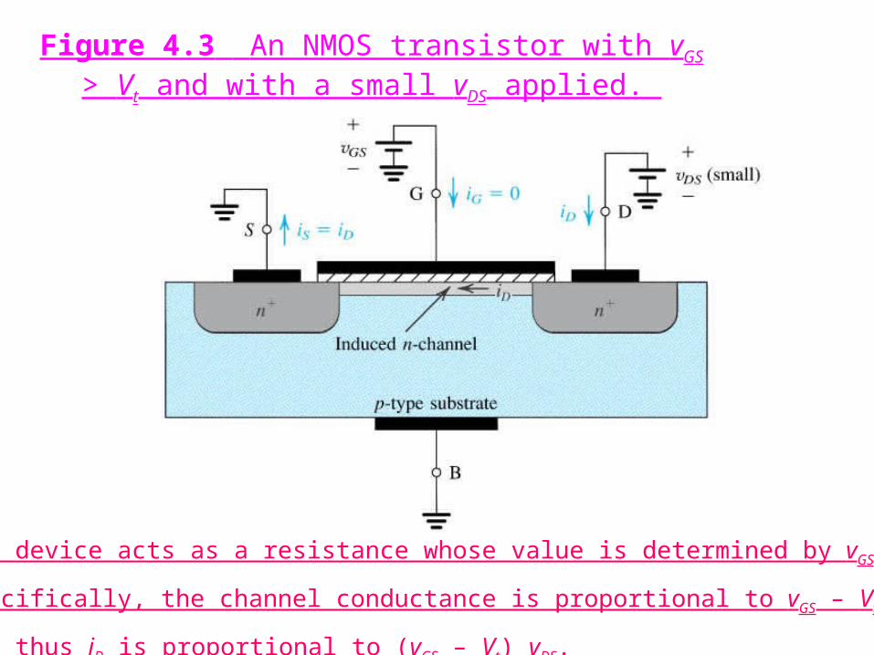
Figure 4.3 An NMOS transistor with vGS > Vt and with a small vDS applied.
The device acts as a resistance whose value is determined by vGS.
Specifically, the channel conductance is proportional to vGS – Vt’
and thus iD is proportional to (vGS – Vt) vDS.
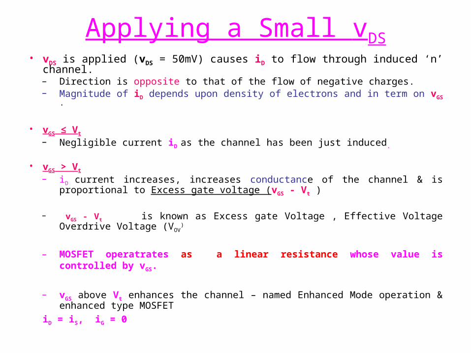
Applying a Small vDS• vDS is applied (vDS = 50mV) causes iD to flow through induced ‘n’ channel.
– Direction is opposite to that of the flow of negative charges. – Magnitude of iD depends upon density of electrons and in term on vGS .
• vGS ≤ Vt – Negligible current iD as the channel has been just induced.
• vGS > Vt – iD current increases, increases conductance of the channel & is proportional
to Excess gate voltage (vGS - Vt )
– vGS - Vt is known as Excess gate Voltage , Effective Voltage Overdrive Voltage (VOV
)
– MOSFET operatrates as a linear resistance whose value is controlled by vGS.
– vGS above Vt enhances the channel – named Enhanced Mode operation & enhanced type MOSFET
iD = iS, iG = 0
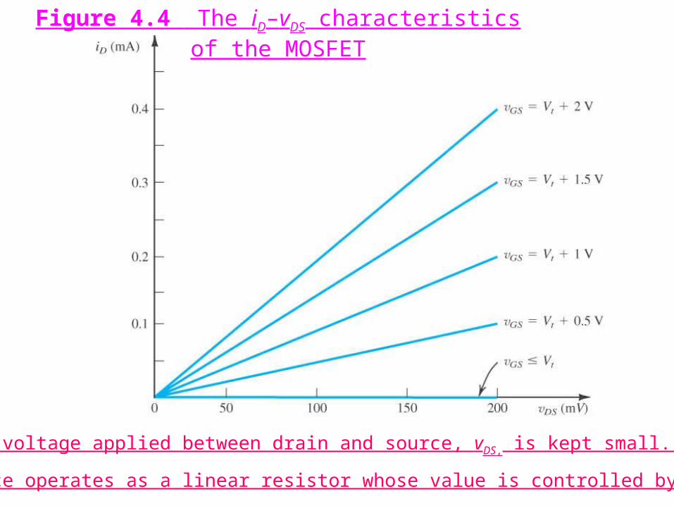
Figure 4.4 The iD–vDS characteristics of the MOSFET
When the voltage applied between drain and source, vDS, is kept small.
The device operates as a linear resistor whose value is controlled by vGS.
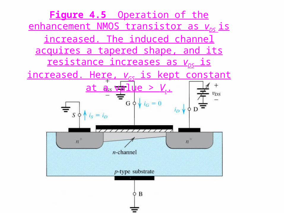
Figure 4.5 Operation of the enhancement NMOS transistor as vDS is increased. The induced channel
acquires a tapered shape, and its resistance increases as vDS is increased. Here, vGS is kept constant at a value >
Vt.
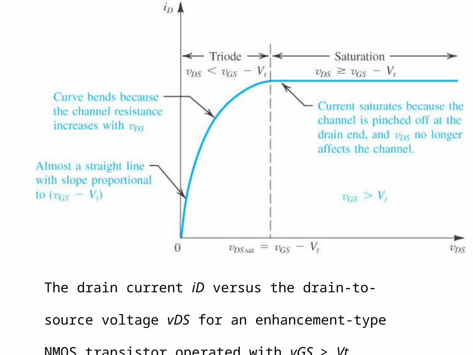
The drain current iD versus the drain-to-source voltage
vDS for an enhancement-type NMOS transistor operated
with vGS > Vt.
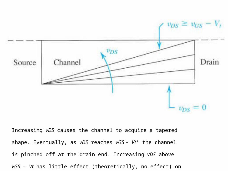
Increasing vDS causes the channel to acquire a tapered shape. Eventually,
as vDS reaches vGS – Vt’ the channel is pinched off at the drain end.
Increasing vDS above vGS – Vt has little effect (theoretically, no effect)
on the channel’s shape.
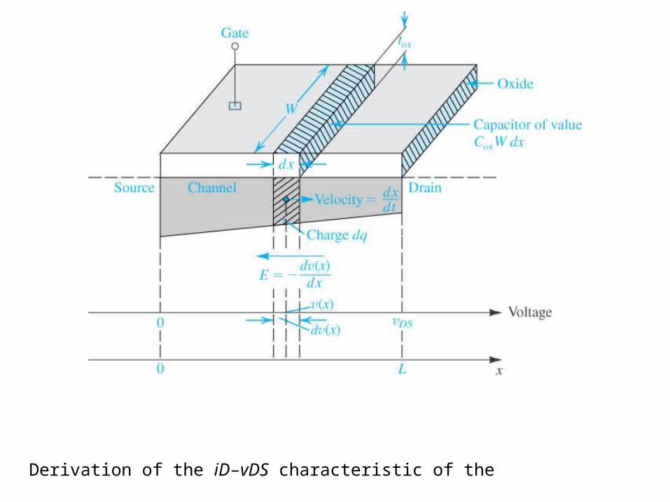
Derivation of the iD–vDS characteristic of the NMOS transistor.

Drain Current iD• Directly Proportional to:
– Mobility of Electrons in the channel μn (μm2/V)
– Gate Capacitance per unit gate area Cox (μF/ μm)
– Width of the substrate (μm)
– Gate-Source Voltage vGS (Volts)
– Drain-Source Voltage v DS (Volts)
• Indirectly Proportional to:– Length of the channel (μm)

iD – vDS relationshipTroide Mode
Saturation Mode

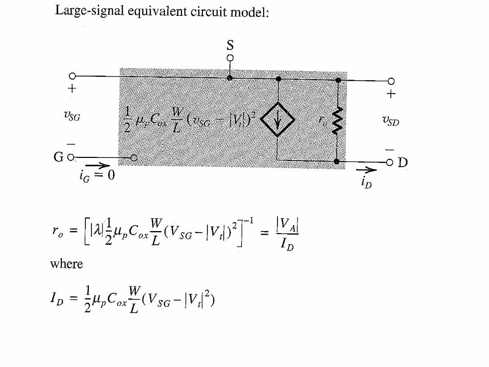
The p Channel MOSFET
• Fabricated on an n-type substrate with p+ regions for Drain & Source
• Holes are the current carriers.
• vGS & vDS are negative
• Threshold voltage Vt is negative.
• Both NMOS & PMOS are utilized in Complementary MOS or CMOS circuits

Cross-section of a CMOS integrated circuit. Note that the PMOS transistor is formed in
a separate n-type region, known as an n well. Another arrangement is also possible in
which an n-type body is used and the n device is formed in a p well. Not shown are the
connections made to the p-type body and to the n well; the latter functions as the body
terminal for the p-channel device.
Complementary MOS or CMOS
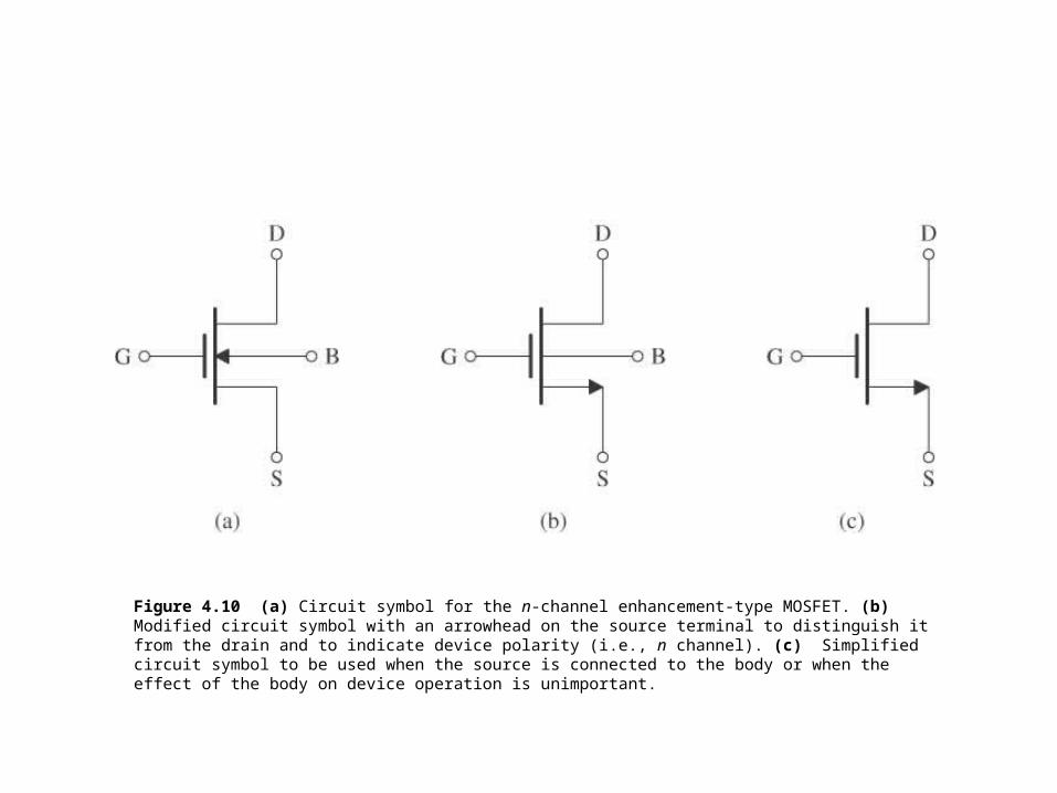
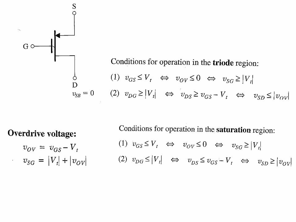
Figure 4.10 (a) Circuit symbol for the n-channel enhancement-type MOSFET. (b) Modified circuit symbol with an arrowhead on the source terminal to distinguish it from the drain and to indicate device polarity (i.e., n channel). (c) Simplified circuit symbol to be used when the source is connected to the body or when the effect of the body on device operation is unimportant.
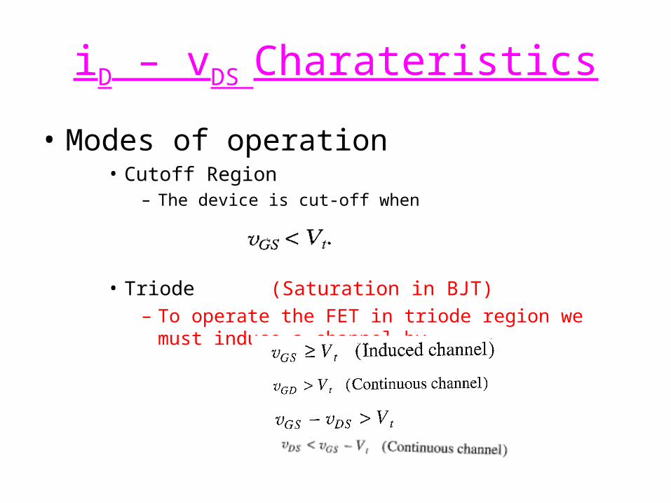
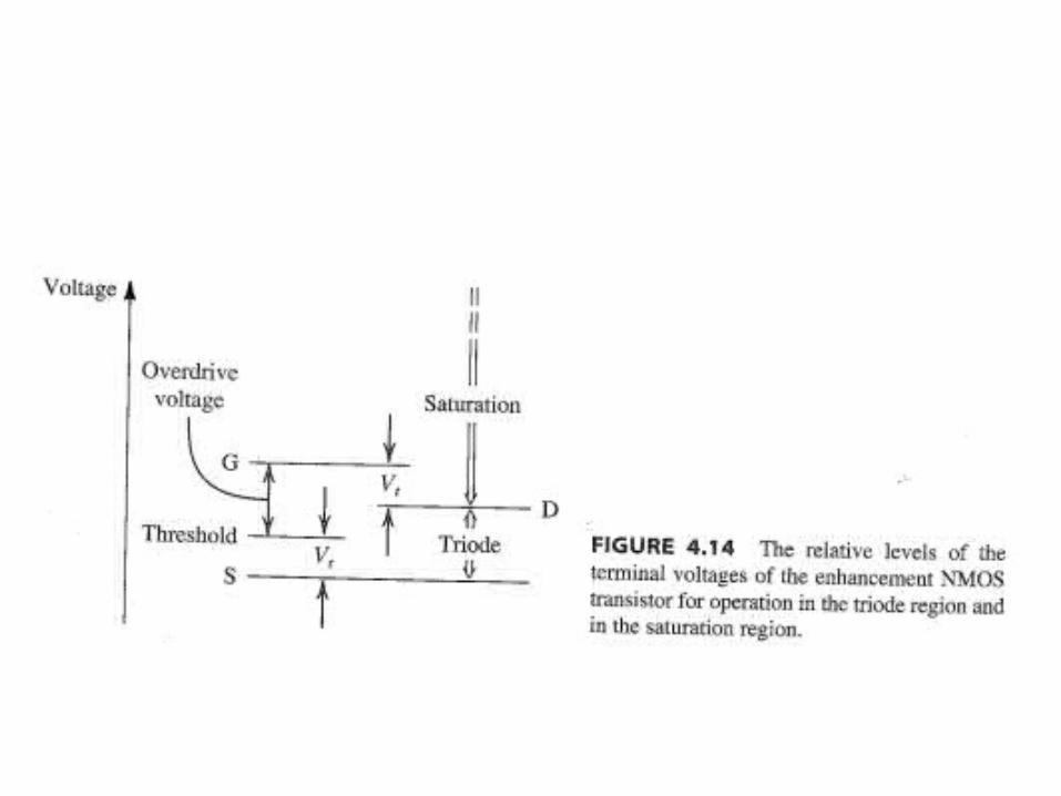
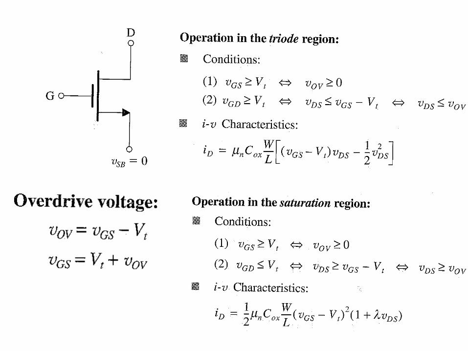
• Modes of operation• Cutoff Region
– The device is cut-off when
• Triode (Saturation in BJT)– To operate the FET in triode region we must induce a
channel by
iD – vDS Charateristics
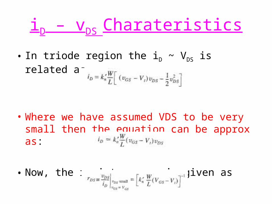
• In triode region the iD ~ VDS is related as
• Where we have assumed VDS to be very small then the equation can be approx as:
• Now, the resistance rDS is given as
iD – vDS Charateristics
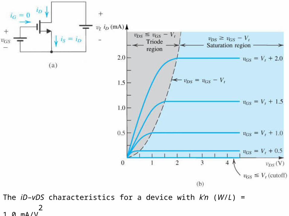
The iD–vDS characteristics for a device with k’n (W/L) = 1.0 mA/V2
.
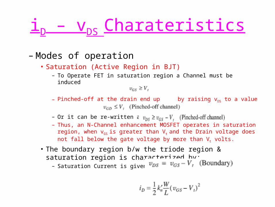
– Modes of operation• Saturation (Active Region in BJT)
– To Operate FET in saturation region a Channel must be induced
– Pinched-off at the drain end up by raising vDS to a value
– Or it can be re-written as
– Thus, an N-Channel enhancement MOSFET operates in saturation region, when vGS is greater than Vt and the Drain voltage does not fall below the gate voltage by more than Vt volts.
• The boundary region b/w the triode region & saturation region is characterized by:
– Saturation Current is given as:
iD – vDS Charateristics
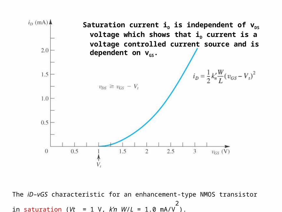
The iD–vGS characteristic for an enhancement-type NMOS transistor in saturation (Vt =
1 V, k’n W/L = 1.0 mA/V2
).
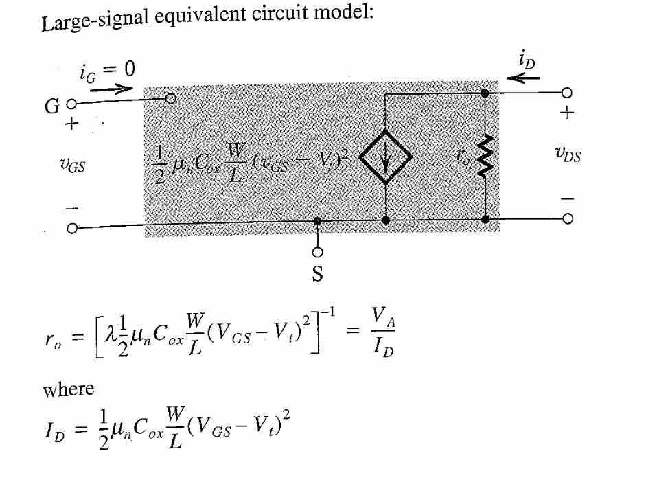
Saturation current iD is independent of vDS voltage which shows that iD current is a voltage controlled current source and is dependent on vGS.

Large-signal equivalent-circuit model of an n-channel MOSFET
operating in the saturation region.

Increasing vDS beyond vDSsat causes the channel pinch-off
point to move slightly away from the drain, thus reducing the
effective channel length (by DL).
Finite Output Resistance in Saturation
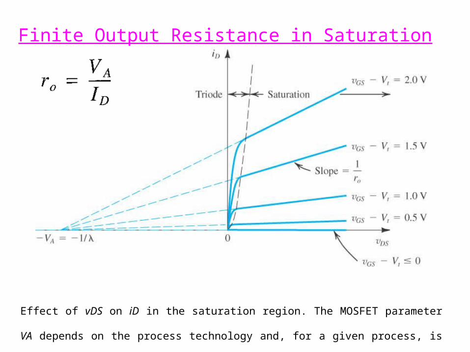
Effect of vDS on iD in the saturation region. The MOSFET parameter VA depends on the
process technology and, for a given process, is proportional to the channel length L.
Finite Output Resistance in Saturation
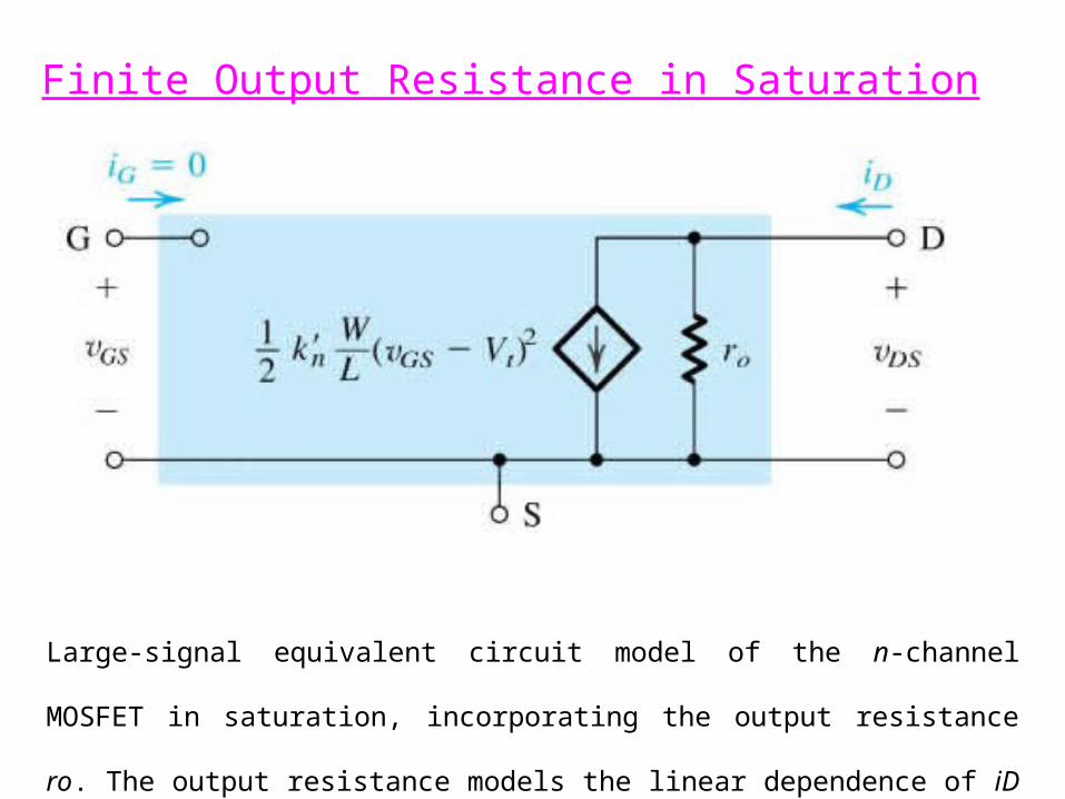
Large-signal equivalent circuit model of the n-channel MOSFET in saturation,
incorporating the output resistance ro. The output resistance models the linear
dependence of iD on vDS
Finite Output Resistance in Saturation
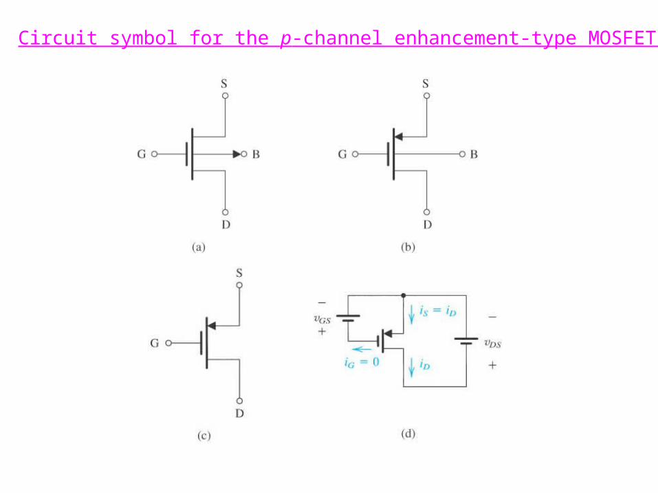
Circuit symbol for the p-channel enhancement-type MOSFET.
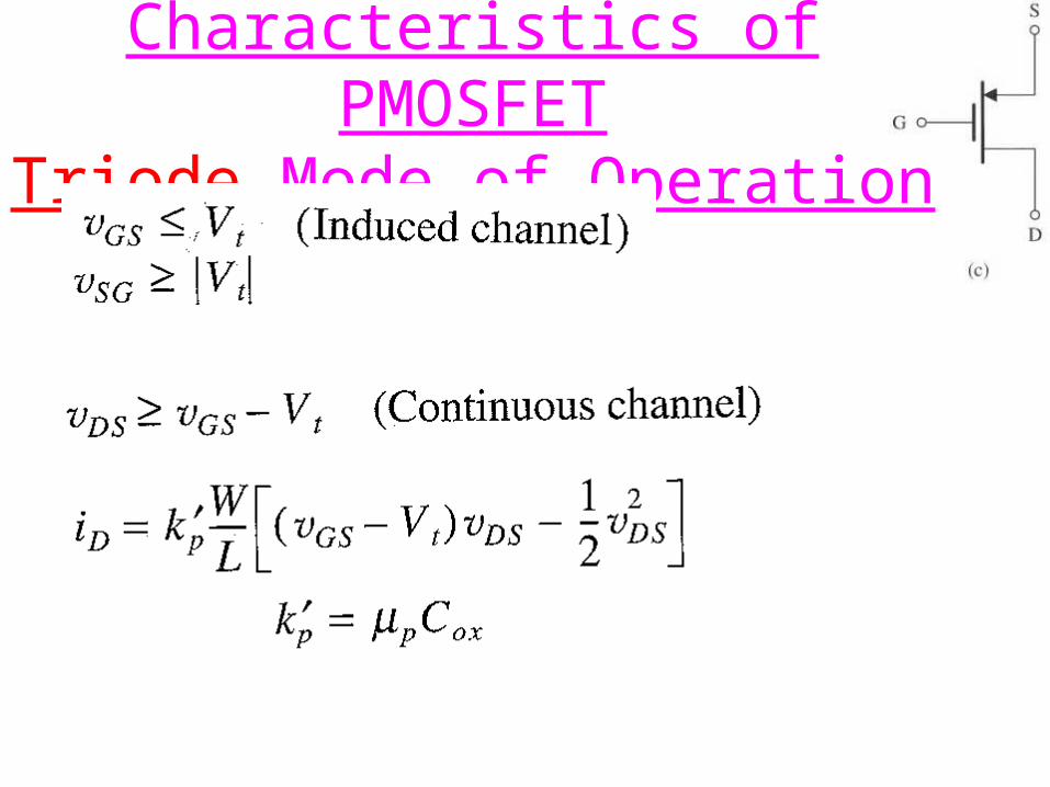
Characteristics of PMOSFETTriode Mode of Operation
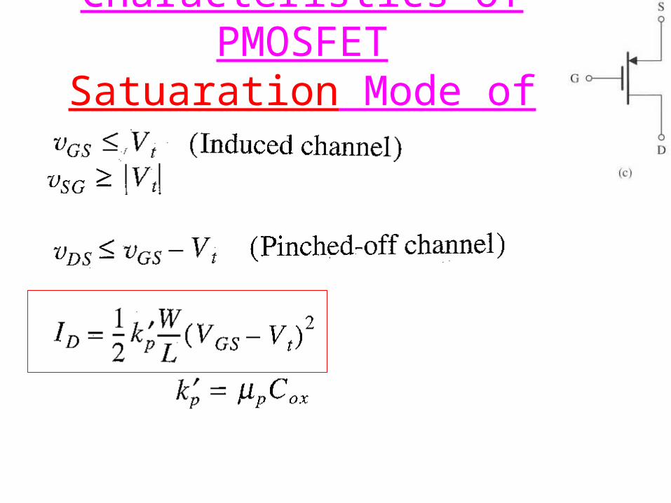
Characteristics of PMOSFETSatuaration Mode of Operation
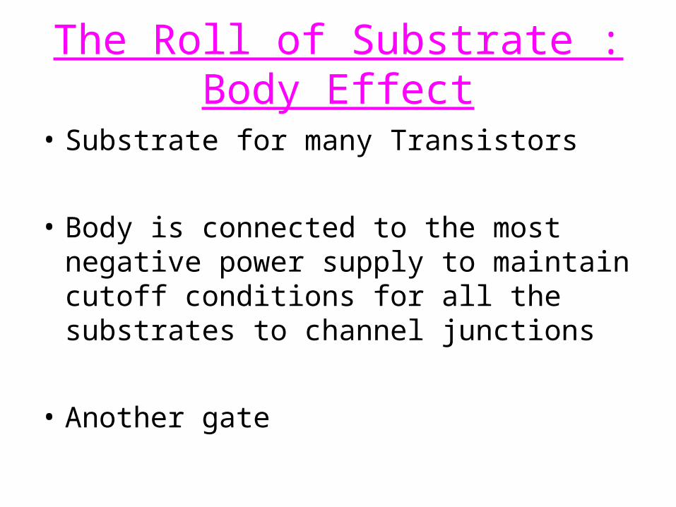
The Roll of Substrate :Body Effect
• Substrate for many Transistors
• Body is connected to the most negative power supply to maintain cutoff conditions for all the substrates to channel junctions
• Another gate
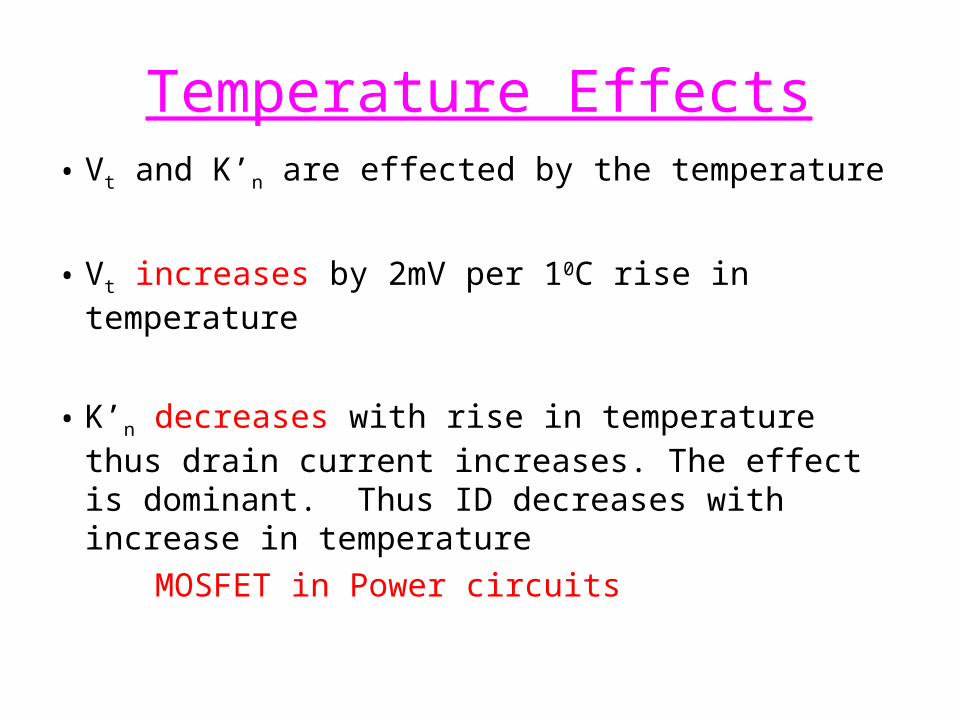
Temperature Effects• Vt and K’n are effected by the temperature
• Vt increases by 2mV per 10C rise in temperature
• K’n decreases with rise in temperature thus drain current increases. The effect is dominant. Thus ID decreases with increase in temperature
MOSFET in Power circuits
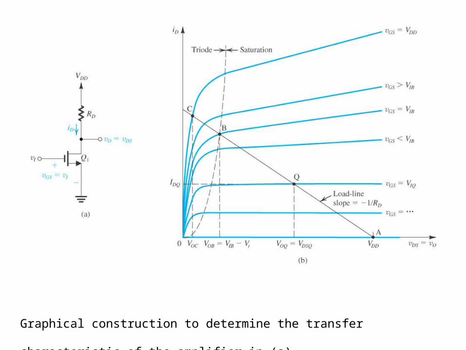
Graphical construction to determine the transfer characteristic of the
amplifier in (a).
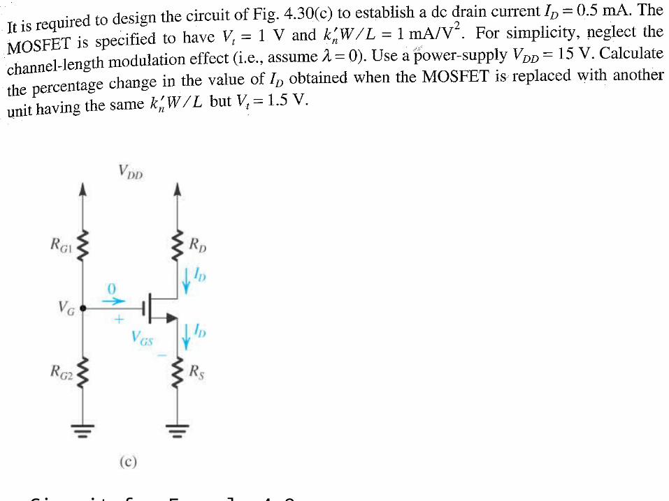
Circuit for Example 4.9.
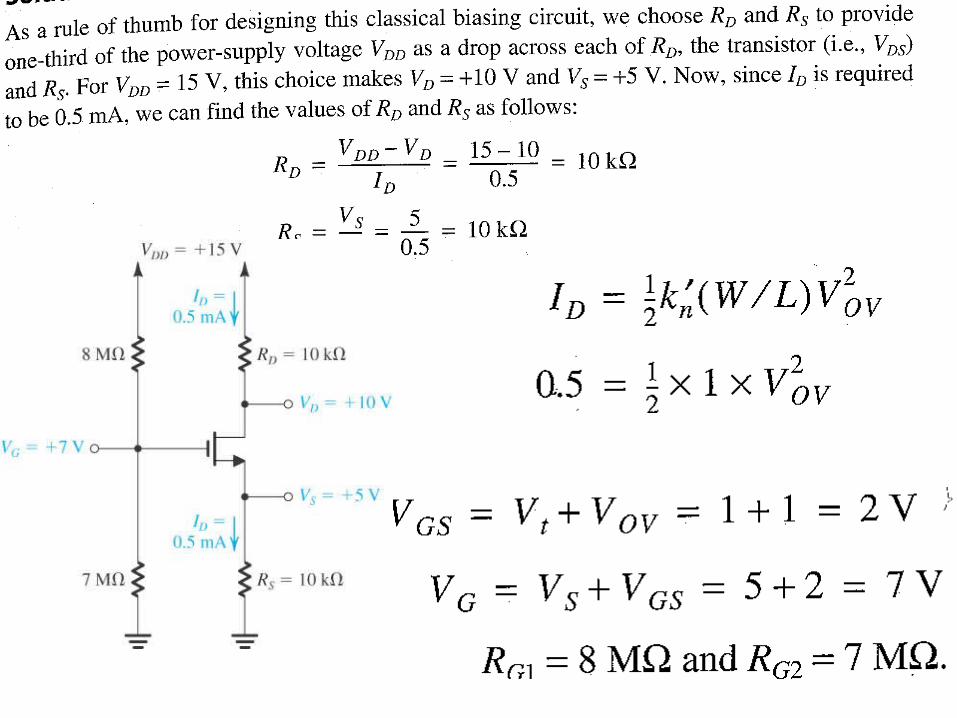
Biasing the MOSFET using a large drain-to-gate feedback resistance, RG.
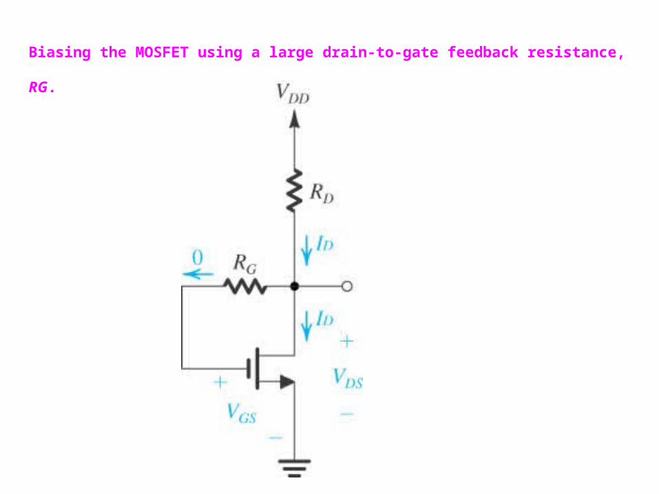
Biasing the MOSFET using a constant-current source
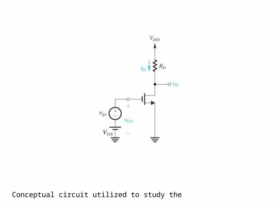
Conceptual circuit utilized to study the operation of the MOSFET
as a small-signal amplifier.
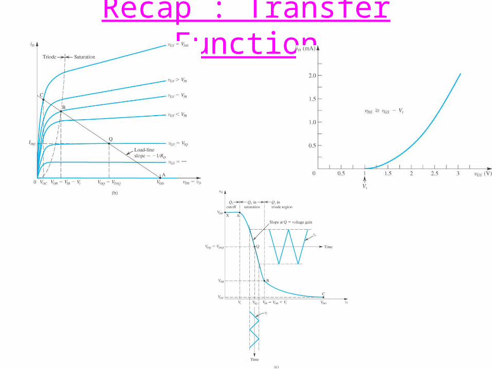
Recap : Transfer Function
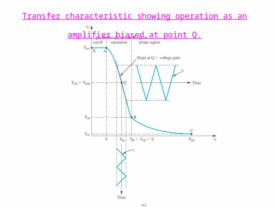
Transfer characteristic showing operation as an amplifier biased at point
Q.
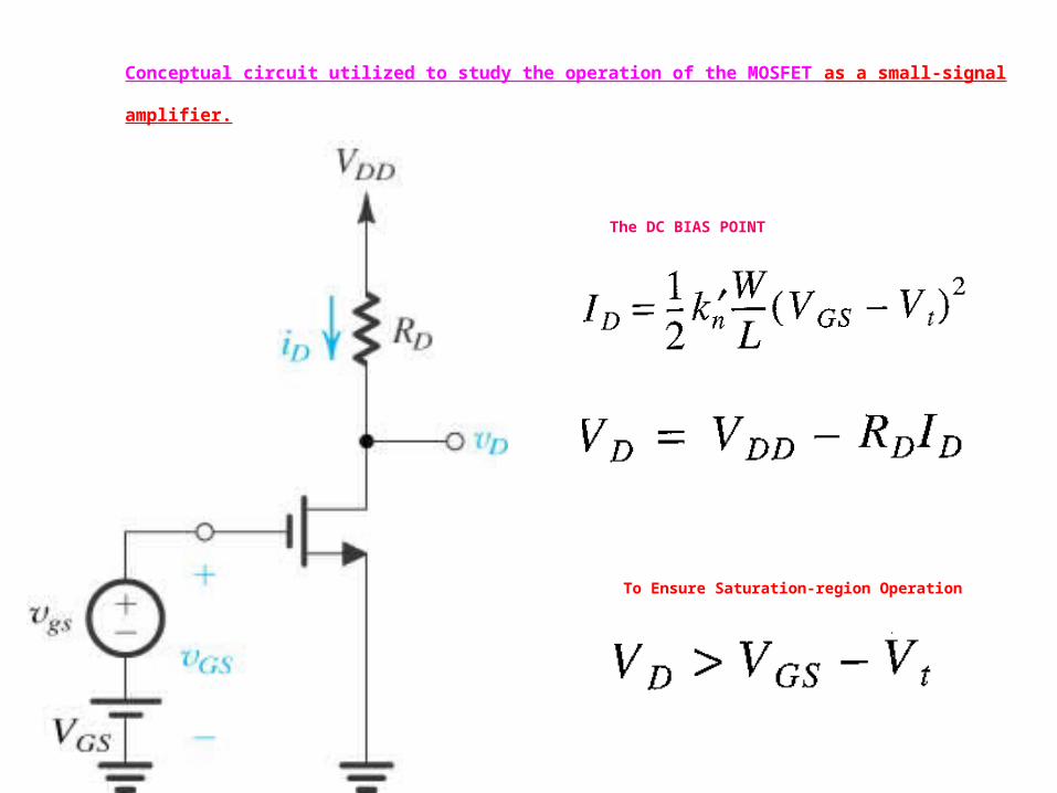
Conceptual circuit utilized to study the operation of the MOSFET as a small-signal amplifier.
The DC BIAS POINT
To Ensure Saturation-region Operation
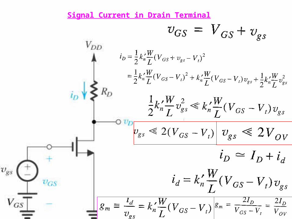
Signal Current in Drain Terminal

Total instantaneous voltages vGS and vD
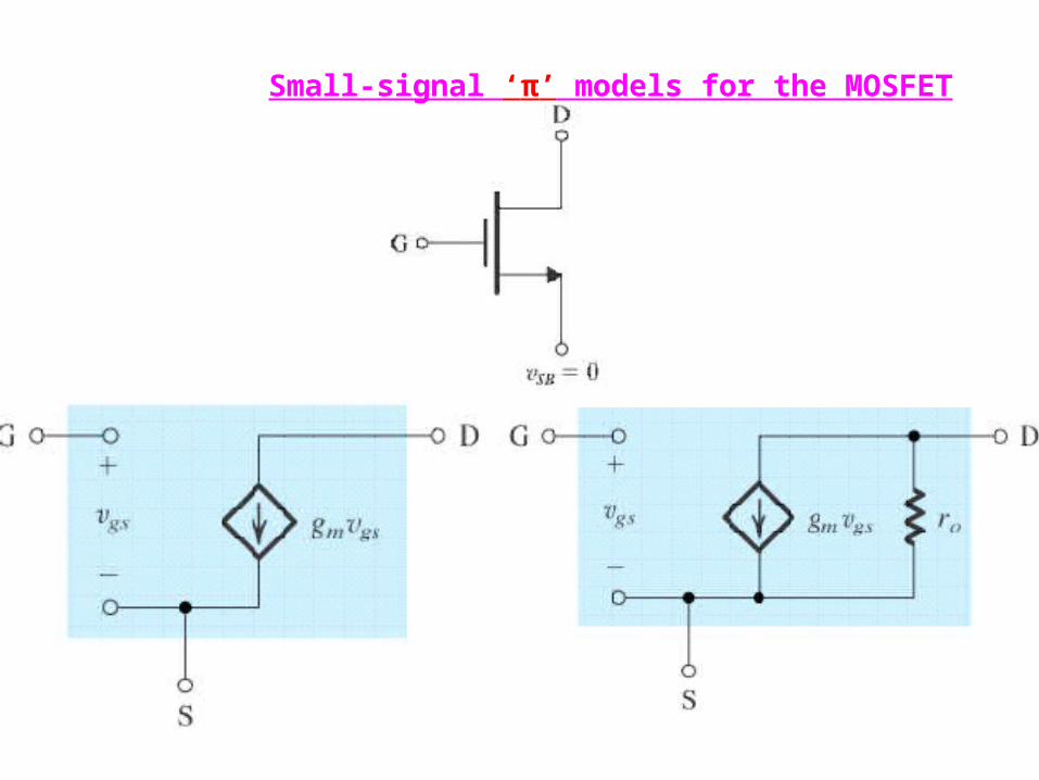
Small-signal ‘π’ models for the MOSFET
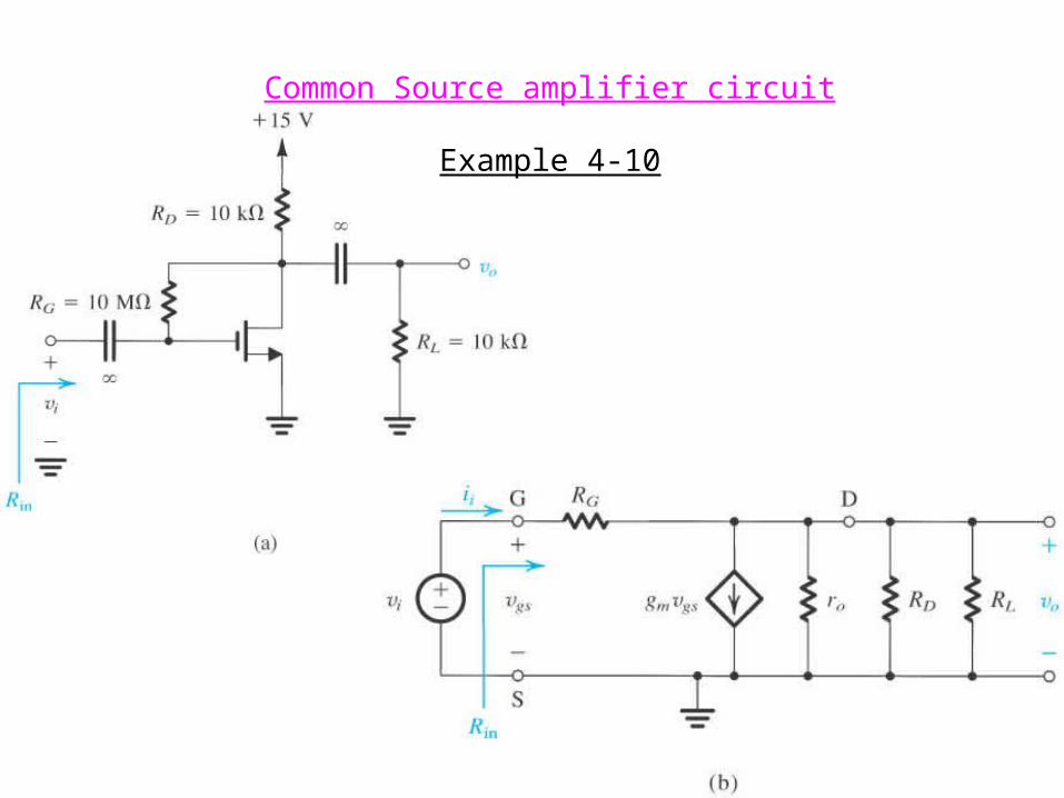
Common Source amplifier circuit
Example 4-10
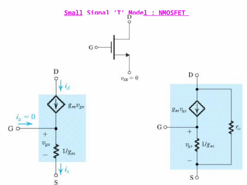
Small Signal ‘T’ Model : NMOSFET
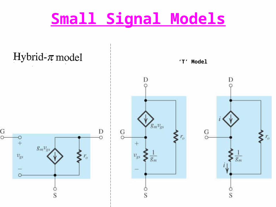
Small Signal Models
‘T’ Model

Single Stage MOS Amplifier
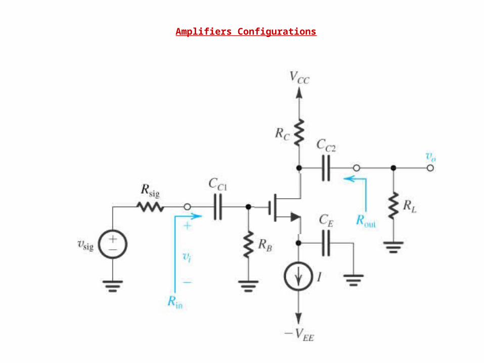
Amplifiers Configurations
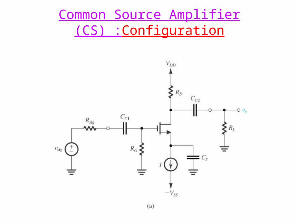
Common Source Amplifier (CS) :Configuration
Common Source Amplifier (CS)• Most widely used
• Signal ground or an ac earth is at the source through a bypass capacitor
• Not to disturb dc bias current & voltages coupling capacitors are used to pass the signal voltages to the input terminal of the amplifier or to the Load Resistance
• CS circuit is unilateral – – Rin does not depend on RL and vice versa
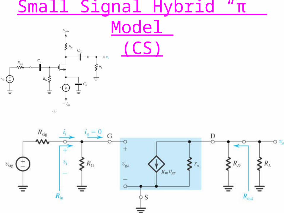
Small Signal Hybrid “π” Model (CS)
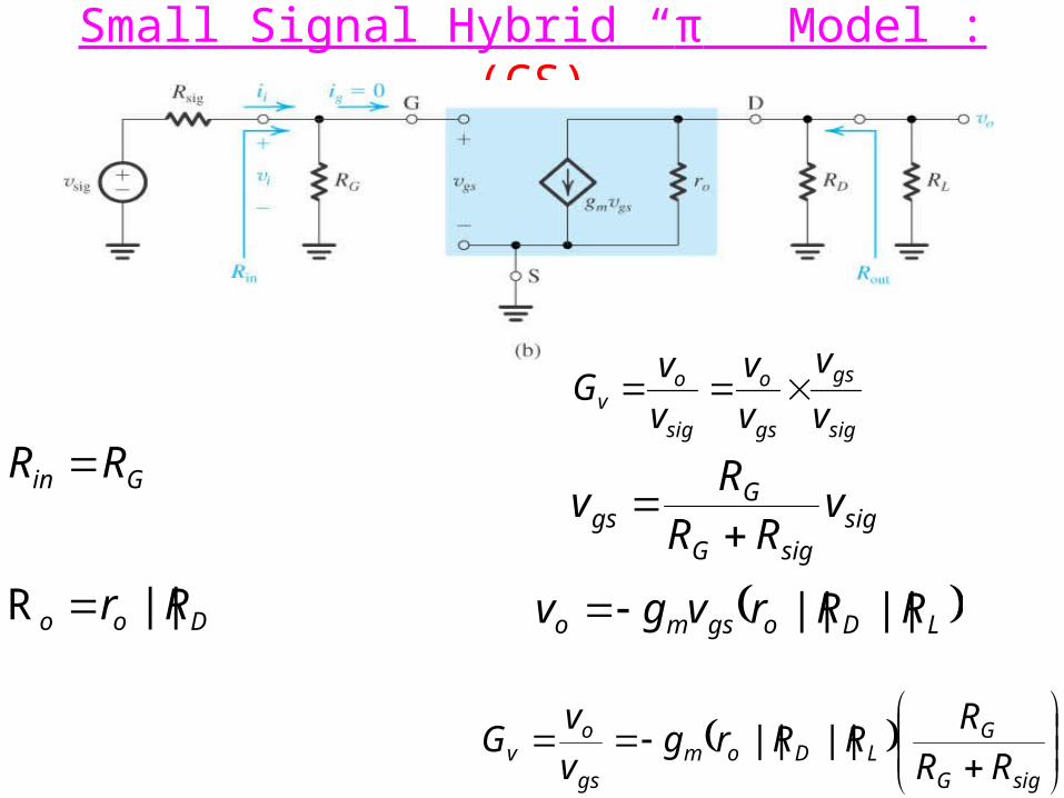
Small Signal Hybrid “π” Model : (CS)
Gin RR sig
sigG
Ggs v
RR
Rv
LDogsmo RRrvgv ||||
sigG
GLDom
gs
ov RR
RRRrg
v
vG ||||
Doo Rr ||R
sig
gs
gs
o
sig
ov v
v
v
v
v
vG
Small-signal analysis performed directly on the amplifier circuit with the MOSFET model implicitly
utilized.
Gin RR
sigG
GLDom
gs
o
RR
RRRrg
v
v||||
Doo Rr ||R
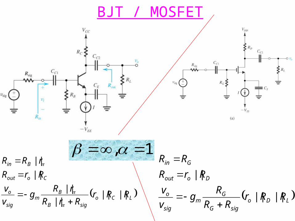
BJT / MOSFET
LCosigB
Bm
sig
o
Coout
Bin
RRrRrR
rRg
v
v
RrR
rRR
||||||
||
||
||
LDosigG
Gm
sig
o
Doout
Gin
RRrRR
Rg
v
v
RrR
RR
||||
||
1,
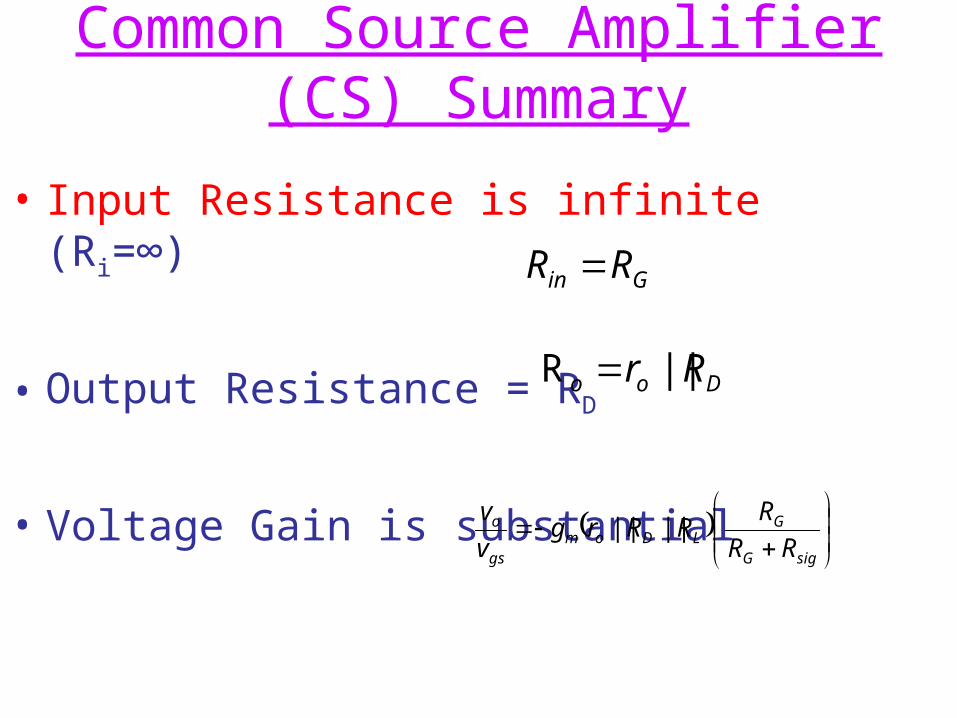
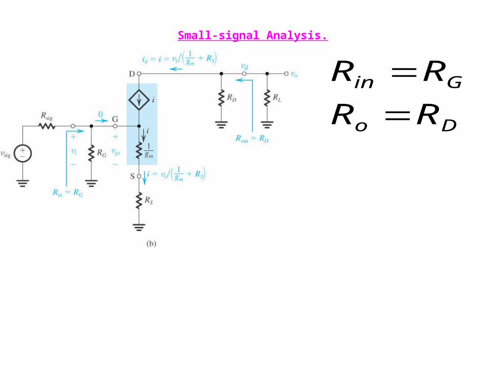
• Input Resistance is infinite (Ri=∞)
• Output Resistance = RD
• Voltage Gain is substantial
Common Source Amplifier (CS) Summary
Gin RR
sigG
GLDom
gs
o
RR
RRRrg
v
v||||
Doo Rr ||R
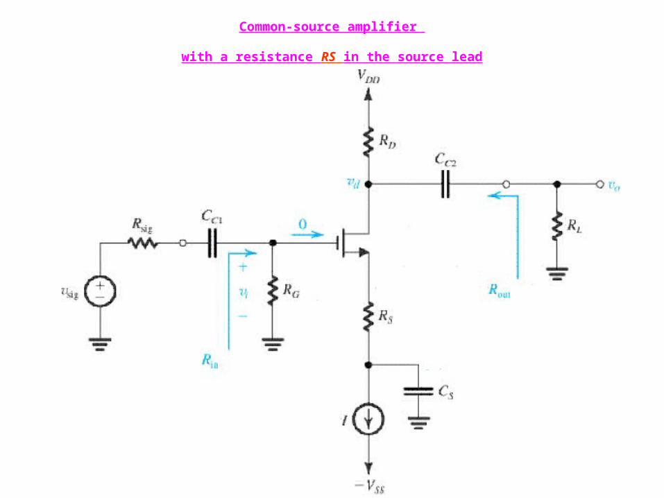
Common-source amplifier
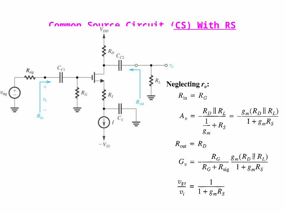
with a resistance RS in the source lead
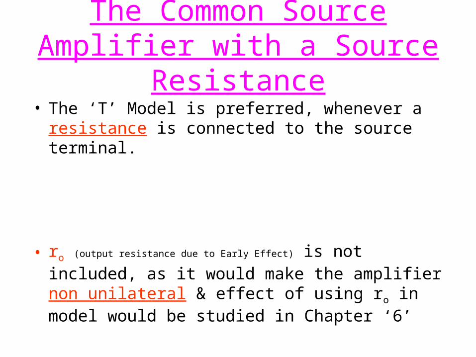
The Common Source Amplifier with a Source Resistance
• The ‘T’ Model is preferred, whenever a resistance is connected to the source terminal.
• ro (output resistance due to Early Effect) is not included, as it would make the amplifier non unilateral & effect of using ro in model would be studied in Chapter ‘6’

Small-signal equivalent circuit with ro neglected.
Sm
g
Rg
vi
1
Do
Gin
RR
RR
Small-signal Analysis.
sig
i
i
gs
gs
o
sig
ov v
v
v
v
v
v
v
vG
Sm
LDm
sigG
Gv
sig
o
sigsigG
Gi
Sm
ii
Sm
mgs
LDgsmo
Rg
RRg
RR
RG
v
v
vRR
Rv
Rg
vv
Rg
gv
RRvgv
1
||
11
1
||
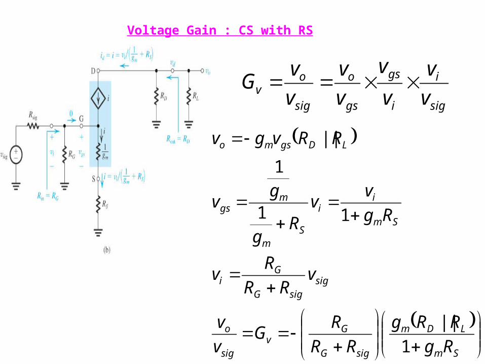
Voltage Gain : CS with RS
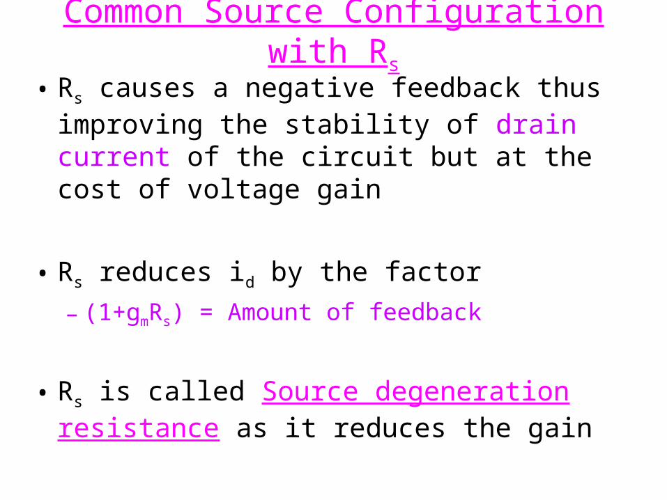
Common Source Configuration with Rs
• Rs causes a negative feedback thus improving the stability of drain current of the circuit but at the cost of voltage gain
• Rs reduces id by the factor
– (1+gmRs) = Amount of feedback
• Rs is called Source degeneration resistance as it reduces the gain
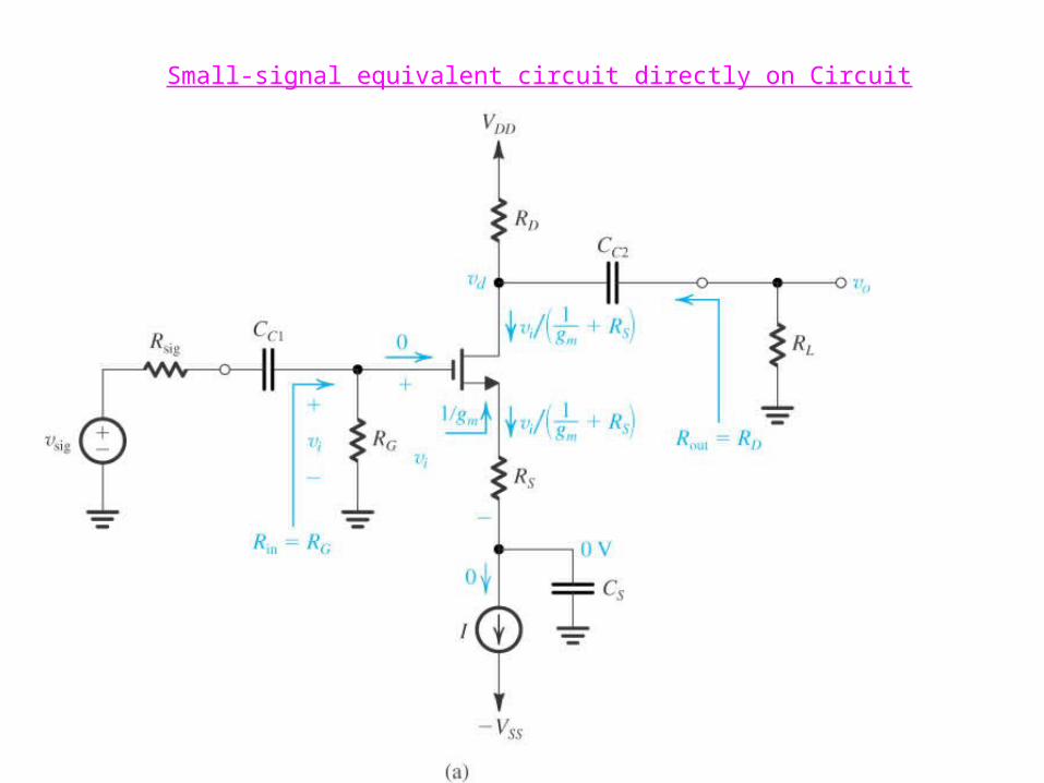
Small-signal equivalent circuit directly on Circuit
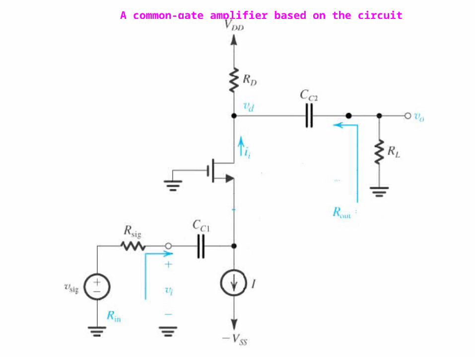
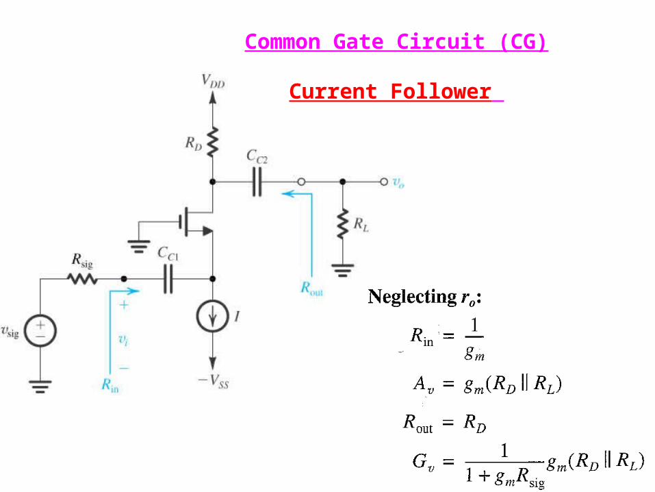
A common-gate amplifier based on the circuit
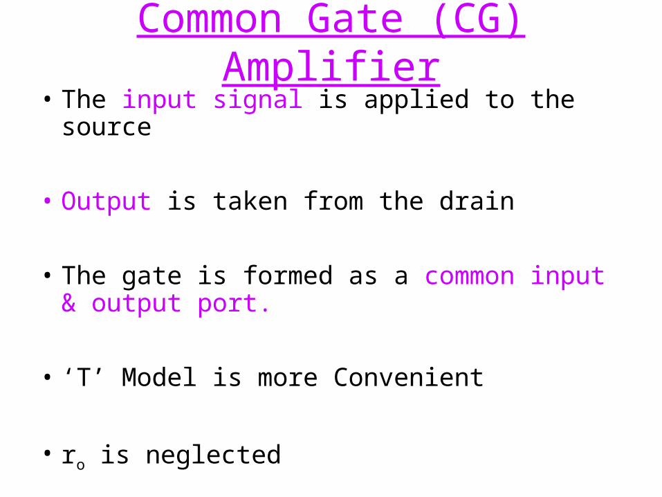
Common Gate (CG) Amplifier• The input signal is applied to the source
• Output is taken from the drain
• The gate is formed as a common input & output port.
• ‘T’ Model is more Convenient
• ro is neglected
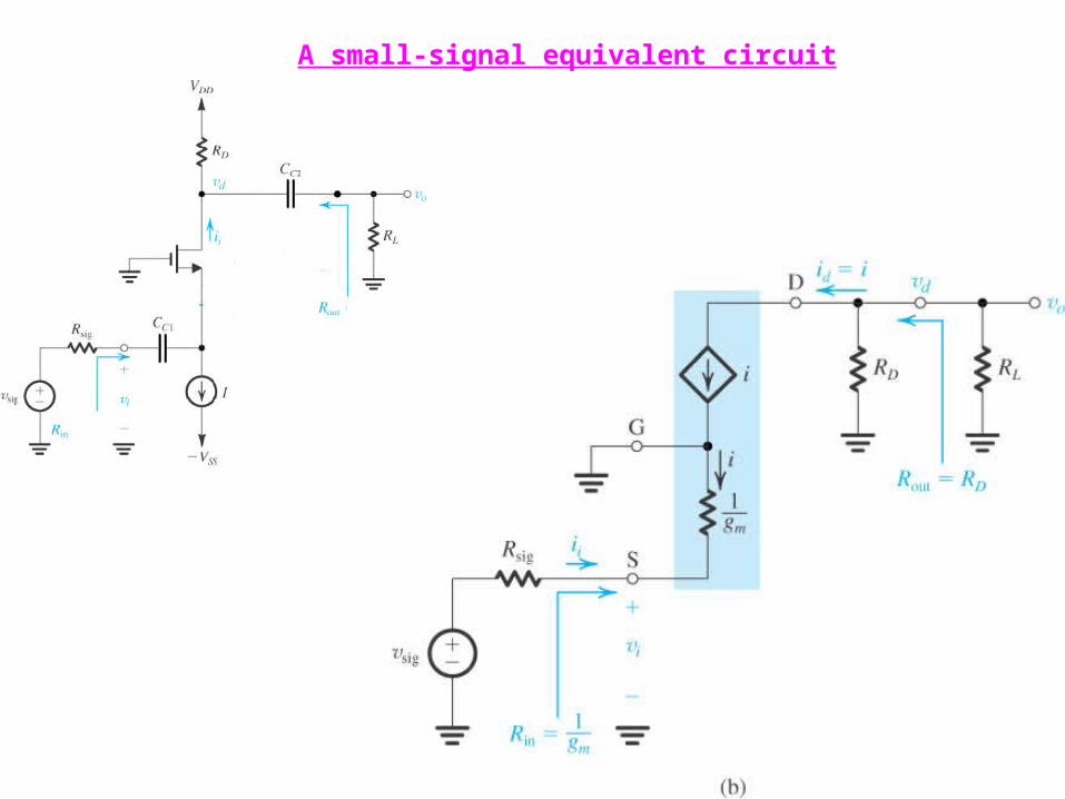
A small-signal equivalent circuit
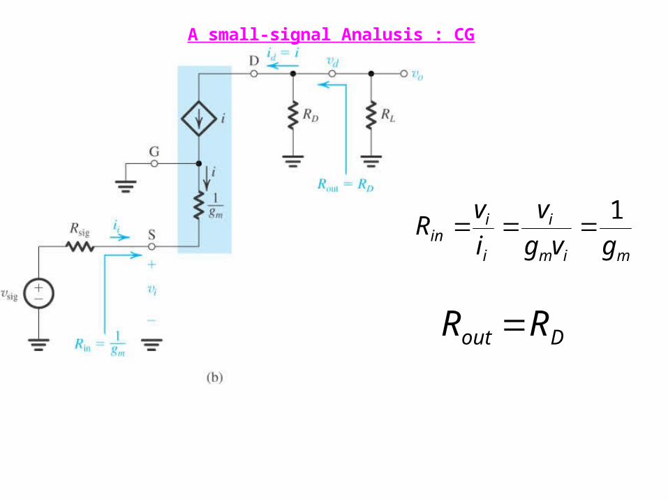
A small-signal Analusis : CG
mim
i
i
iin gvg
v
i
vR
1
Dout RR
A small-signal Analusis : CG
sigm
LDm
sig
ov
sigm
sigsig
sigm
msig
sigin
ini
LDimo
sig
i
i
o
sig
ov
Rg
RRg
v
vG
Rg
vv
Rg
gv
RR
Rv
RRvgv
v
v
v
v
v
vG
1
||
11
1
||

Small signal analysis directly on circuit
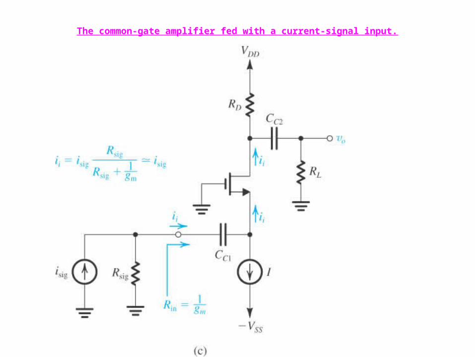
The common-gate amplifier fed with a current-signal input.
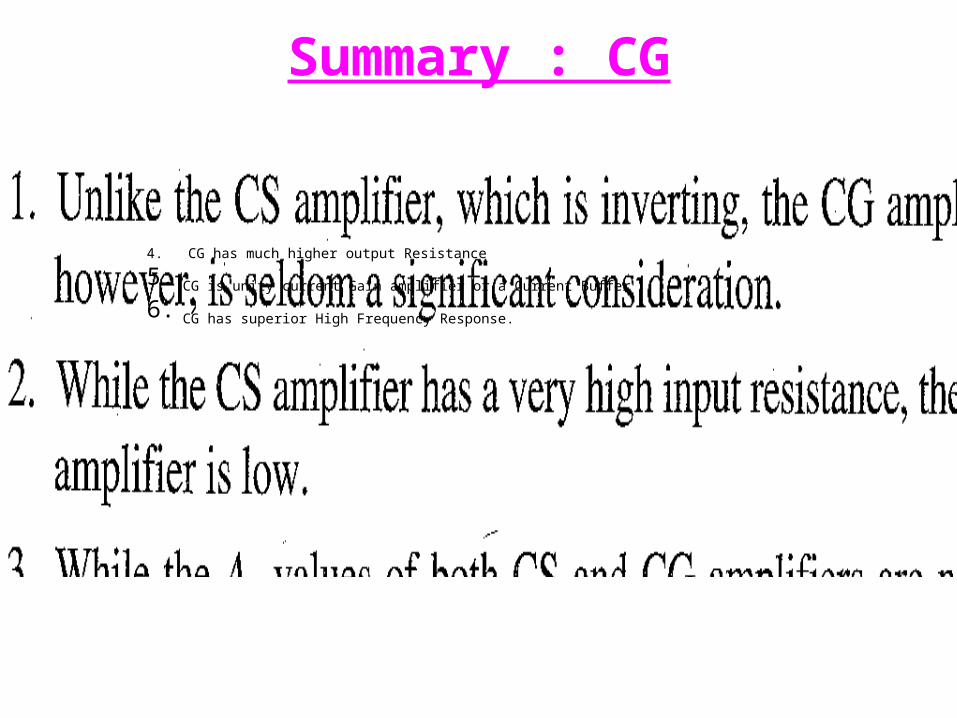
Summary : CG
4. CG has much higher output Resistance
5. CG is unity current Gain amplifier or a Current Buffer
6. CG has superior High Frequency Response.
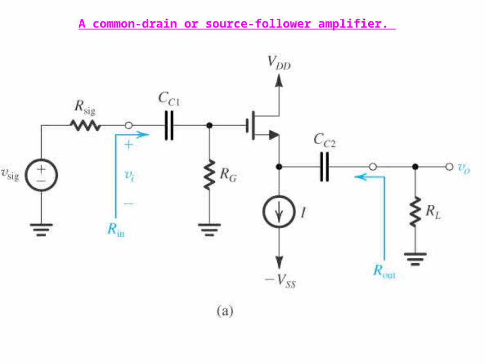
A common-drain or source-follower amplifier.
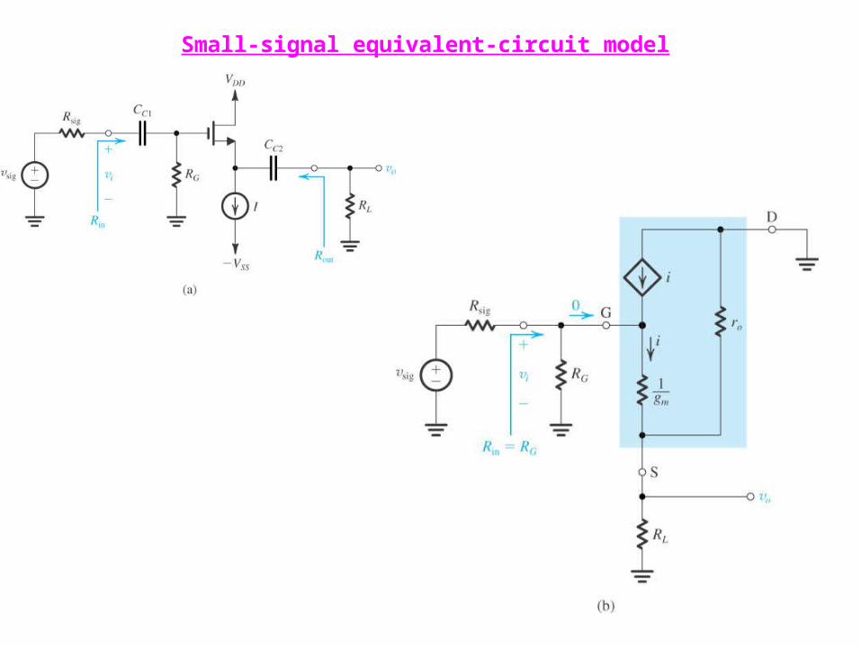
Small-signal equivalent-circuit model

Small-signal Analysis : CD
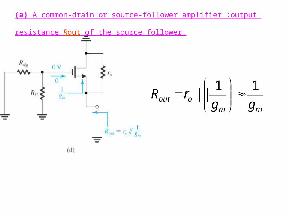
(a) A common-drain or source-follower amplifier :output resistance Rout of the source
follower.
mmoout gg
rR11
||
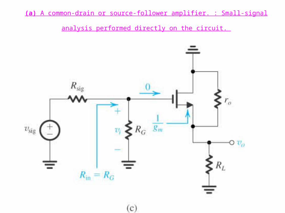
(a) A common-drain or source-follower amplifier. : Small-signal analysis performed directly on the
circuit.

Common Source Circuit (CS)
Common Source Circuit (CS) With RS
Common Gate Circuit (CG)
Current Follower
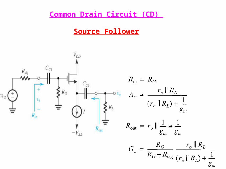
Common Drain Circuit (CD)
Source Follower
Summary & Comparison

Quiz No 4• Draw/Write the Following:
27-03-07
BJT MOSFET
Types npn pnp nMOS pMOS
Symbols
‘π’ Model
T Model
gm
Re/rs
rπ/rg
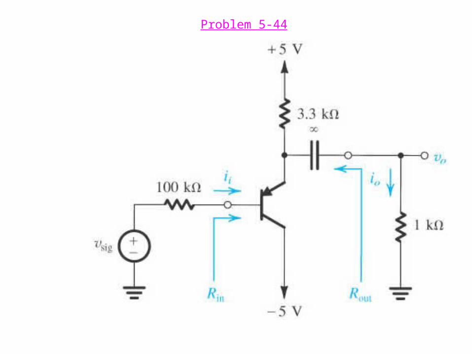
Problem 5-44
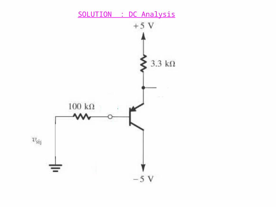
SOLUTION : DC Analysis
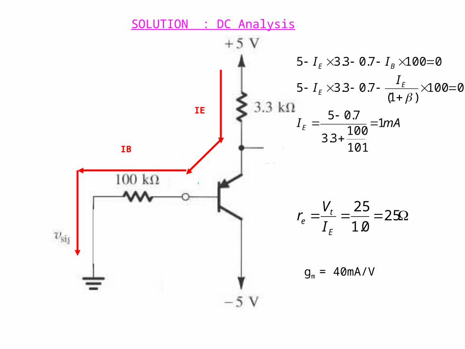
SOLUTION : DC Analysis
IE
mAI
II
II
E
EE
BE
1
101100
3.3
7.05
0100)1(
7.03.35
01007.03.35
250.1
25
E
te I
Vr
IB
gm = 40mA/V
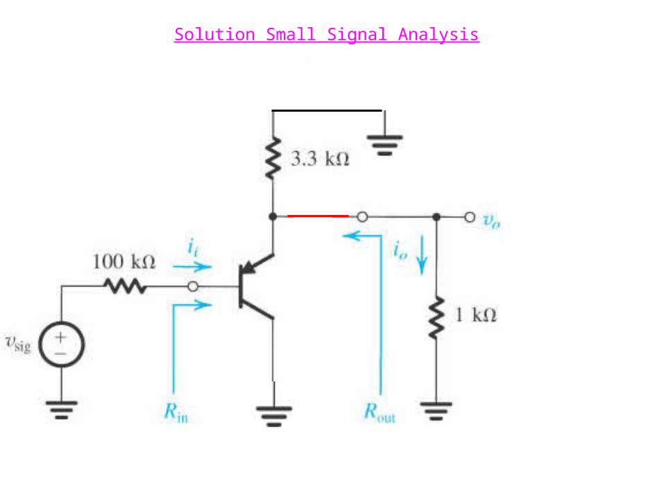
Solution Small Signal Analysis
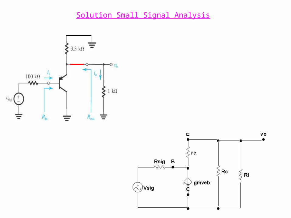
Solution Small Signal Analysis

Solution Small Signal Analysis : Input Resistance
Rin
ib
LCee
b
b
bin RRr
i
v
i
vR ||)1(
)1(
+
vb
-
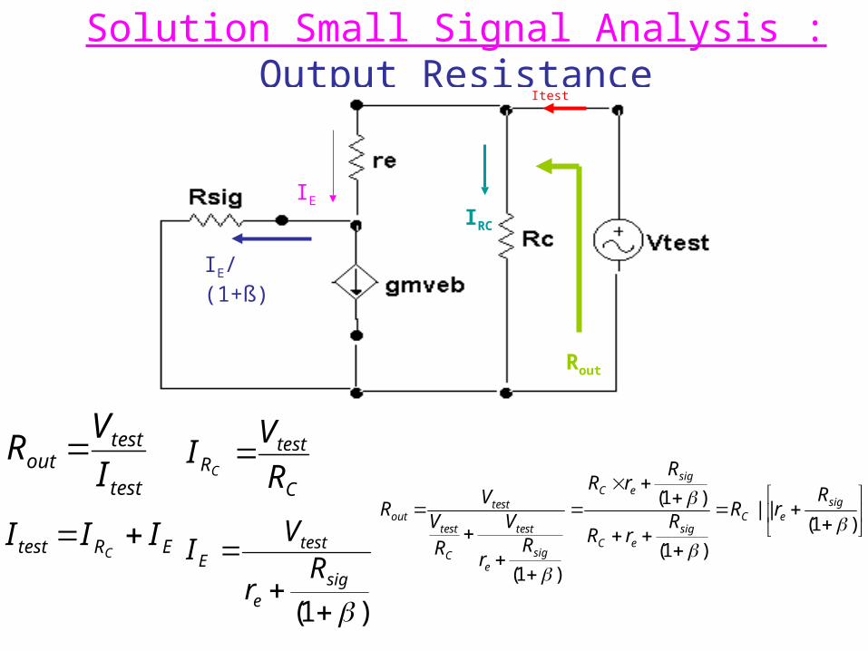
Solution Small Signal Analysis : Output ResistanceItest
IE
IE/(1+ß)
IRC
Rout
test
testout I
VR
)1(||
)1(
)1(
)1(
sigeC
sigeC
sigeC
sige
test
C
test
testout
RrR
RrR
RrR
Rr
VR
VV
R
ERtest IIIC
)1(
sig
e
testE R
r
VI
C
testR R
VI
C
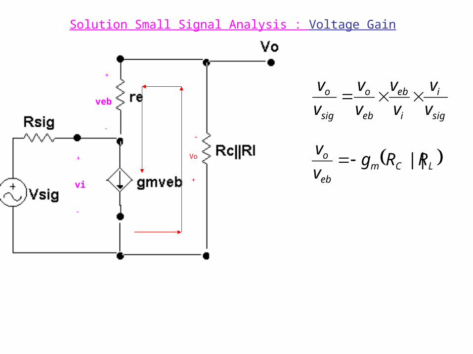
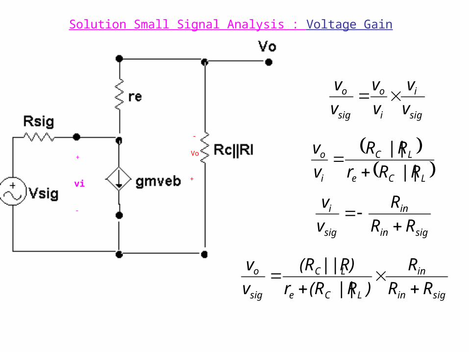
Solution Small Signal Analysis : Voltage Gain
+
-
LCmeb
o RRgv
v||+
-
vi
+
-
veb
sig
i
i
eb
eb
o
sig
o
v
v
v
v
v
v
v
v
Vo
Solution Small Signal Analysis : Voltage gain
sig
i
i
eb
eb
o
sig
o
v
v
v
v
v
v
v
v
LCmeb
o RRgv
v||+
-
vi
+
-
veb
LCe
e
i
eb
RRr
r
v
v
||
Solution Small Signal Analysis : Voltage Gain
sig
i
i
eb
eb
o
sig
o
v
v
v
v
v
v
v
v
LCmeb
o RRgv
v||
+
-
vi LCe
e
i
eb
RRr
r
v
v
||
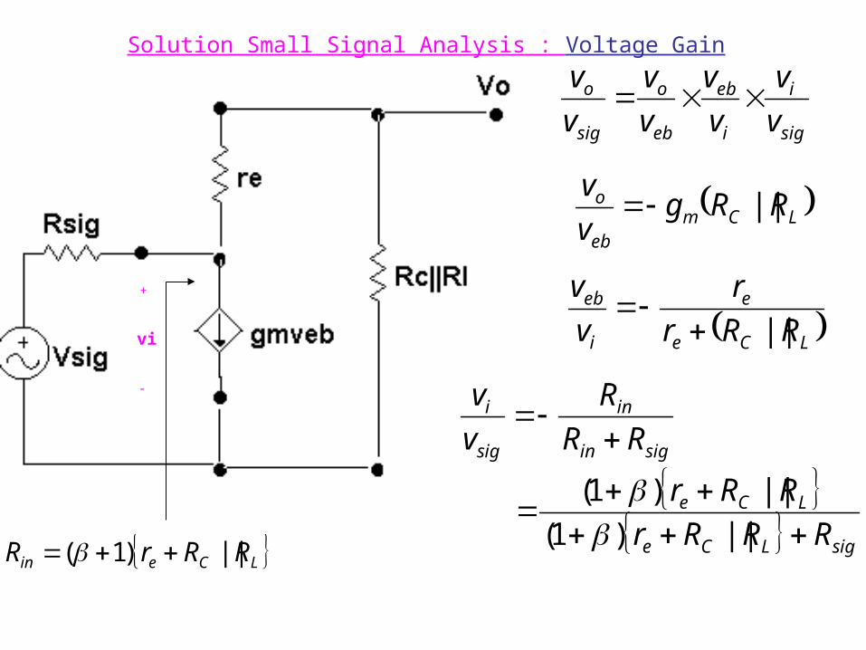
LCein RRrR ||)1(
sigLCe
LCe
sigin
in
sig
i
RRRr
RRr
RR
R
v
v
||)1(
||)1(
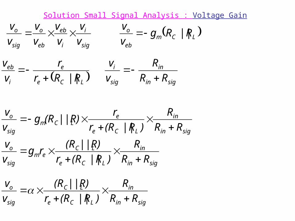
Solution Small Signal Analysis : Voltage Gain
sig
i
i
eb
eb
o
sig
o
v
v
v
v
v
v
v
v LCm
eb
o RRgv
v||
LCe
e
i
eb
RRr
r
v
v
||
sigin
in
LCe
eLCm
sig
o
RR
R
)R(Rr
r)||R(Rg
v
v
||
sigin
in
sig
i
RR
R
v
v
sigin
in
LCe
LC
sig
o
RR
R
)R(Rr
)||R(R
v
v
||
sigin
in
LCe
LCem
sig
o
RR
R
)R(Rr
)||R(Rrg
v
v
||
Solution Small Signal Analysis : Voltage Gain
+
-
LCe
LC
i
o
RRr
RR
v
v
||
||
+
-
vi
sig
i
i
o
sig
o
v
v
v
v
v
v
sigin
in
sig
i
RR
R
v
v
sigin
in
LCe
LC
sig
o
RR
R
)R(Rr
)||R(R
v
v
||
Vo
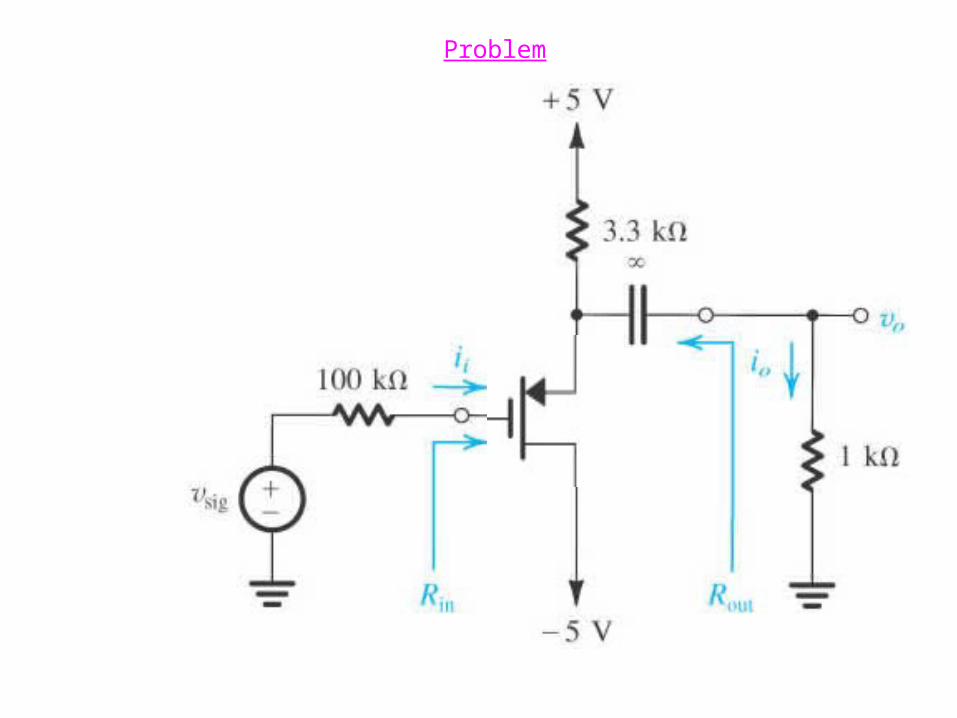
Problem
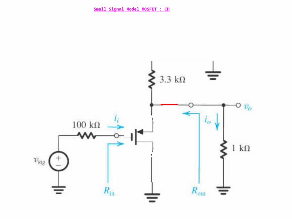
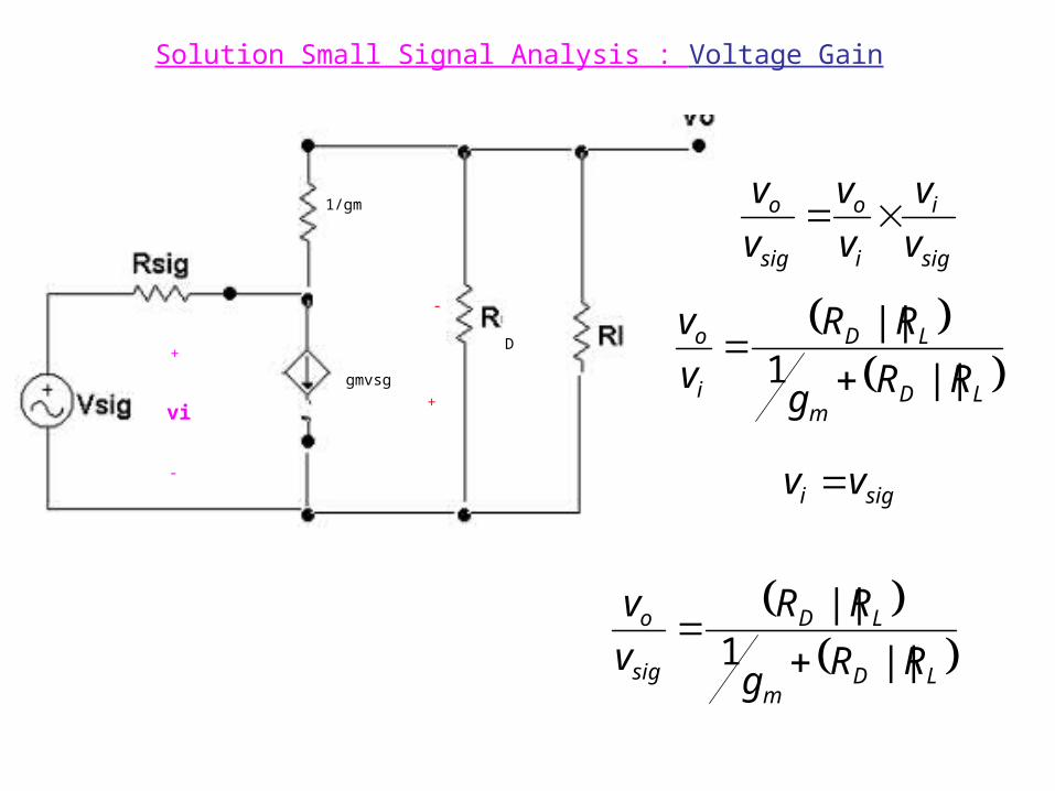
Small Signal Model MOSFET : CD

Solution Small Signal Analysis
1/gm
gmvsg
D
1/gm
gmvsg
D
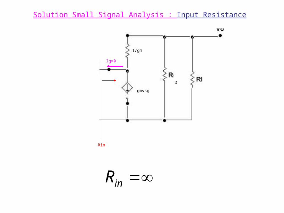
Solution Small Signal Analysis : Input Resistance
Rin
Ig=0
inR
1/gm
gmvsg
D
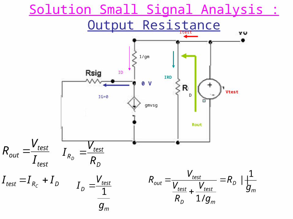
Solution Small Signal Analysis : Output ResistanceItest
ID
IG=0
IRD
Rout
test
testout I
VR
mD
m
test
D
test
testout g
R
gV
RV
VR
1||
/1
DRtest IIIC
m
testD
g
VI
1
D
testR R
VI
D
Vtest
0 V
1/gm
gmvsg
D
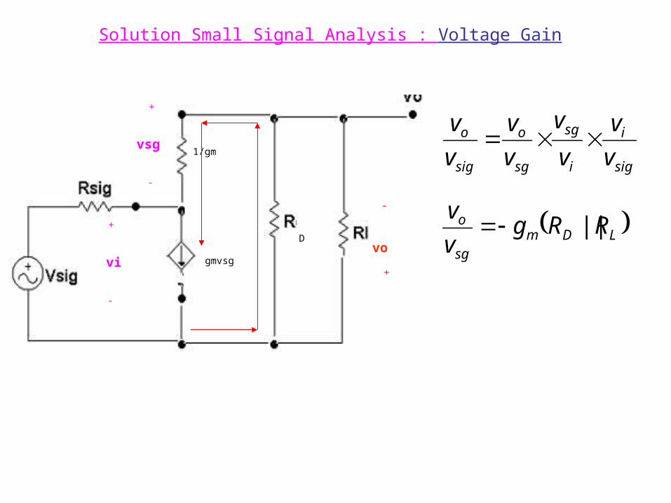
Solution Small Signal Analysis : Voltage Gain
+
-
LDmsg
o RRgv
v||+
-
vi
+
-
vsg
sig
i
i
sg
sg
o
sig
o
v
v
v
v
v
v
v
v
vo
1/gm
gmvsg
D
Solution Small Signal Analysis : Voltage gain
+
-
vi
+
-
vsg
LDm
m
i
sg
RRg
g
v
v
||1
1
1/gm
gmvsg
D
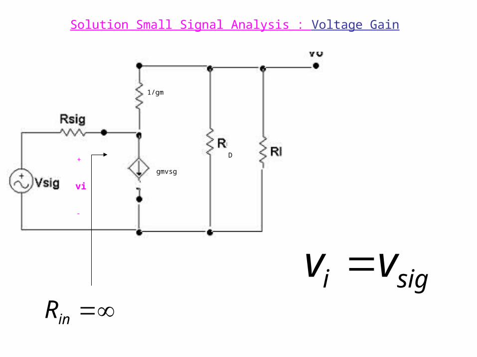
Solution Small Signal Analysis : Voltage Gain
+
-
vi
inRsigi vv
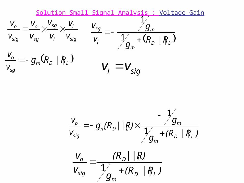
Solution Small Signal Analysis : Voltage Gain
)R(Rg
g)||R(Rg
v
v
LDm
mLDm
sig
o
||1
1
sigi vv LDmsg
o RRgv
v||
sig
i
i
sg
sg
o
sig
o
v
v
v
v
v
v
v
v
LDm
m
i
sg
RRg
g
v
v
||1
1
)R(Rg
)||R(R
v
v
LDm
LD
sig
o
||1
1/gm
gmvsg
D
Solution Small Signal Analysis : Voltage Gain
+
- LD
m
LD
i
o
RRg
RR
v
v
||1||
+
-
vi
sig
i
i
o
sig
o
v
v
v
v
v
v
sigi vv
LD
m
LD
sig
o
RRg
RR
v
v
||1||
Solution Small Signal Analysis
LCein RRrR ||)1(
)1(
||
sigeCout
RrRR
sigin
in
LCe
LC
sig
o
RR
R
)R(Rr
)||R(R
v
v
||
1
inR
mDout g
RR1
||
LD
m
LD
sig
o
RRg
RR
v
v
||1||
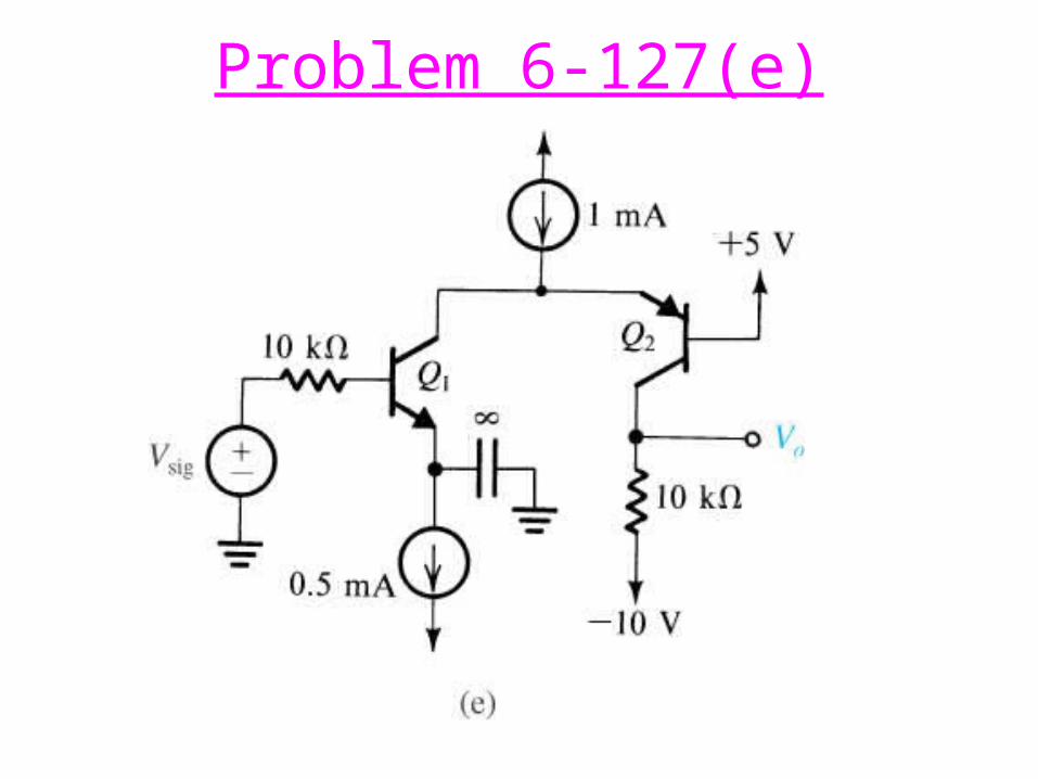
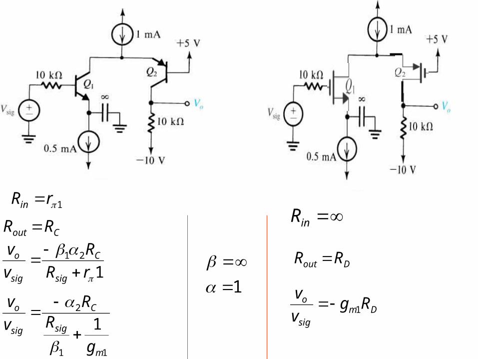
Problem 6-127(e)

DC Analysis 6-127(e)
mAI
AI
mAI
C
B
E
5.0
05101/5.0
5.0
100
1
1
1
mAI
AI
mAI
C
B
E
5.0
05101/5.0
5.0
100
2
2
2
eActiveinQ
VVVVV
VV
BC
C
mod
6.44.054.0
5105.010
2
22
2
eActiveinQ
VVVV
VV
BC
C
mod
4.04.0)10(5104.0
3.47.05
1
311
1
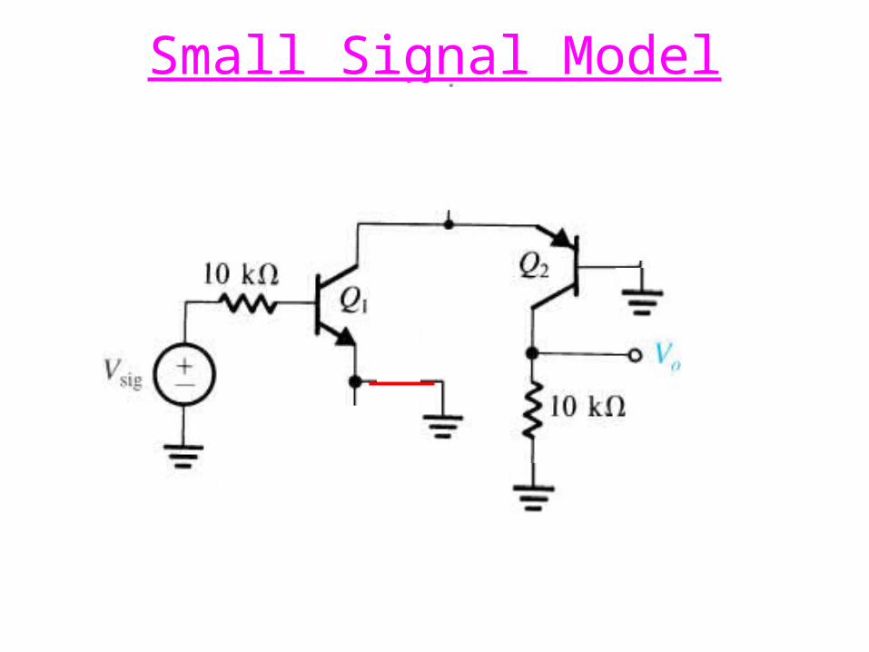
Small Signal Model
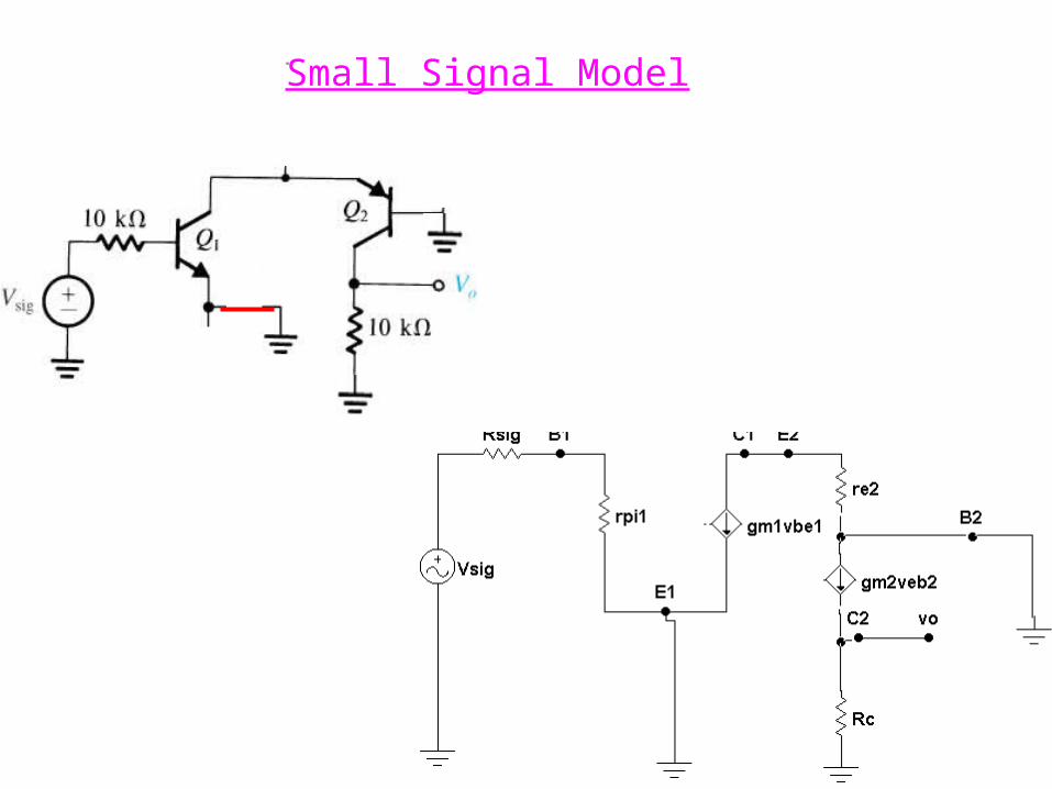
Small Signal Model
Small Signal Model
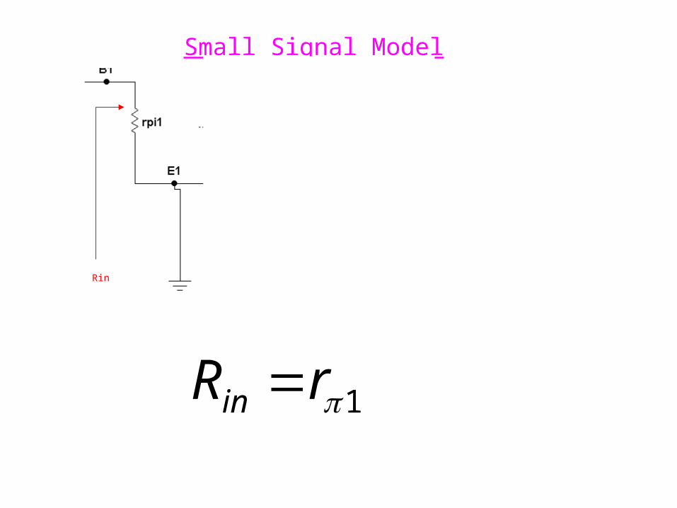
Rin
1rRin
Small Signal Model
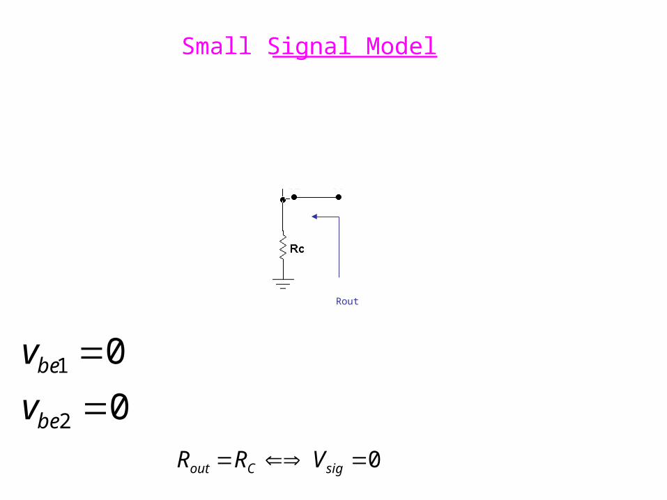
Rout
0 sigCout VRR
+
vbe1
-
01 bev
+
vbe2
-
02 bev
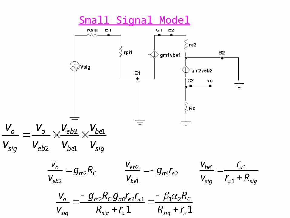
Small Signal Model
sigsig
be
Rr
r
v
v
1
11
sig
be
be
eb
eb
o
sig
o
v
v
v
v
v
v
v
v 1
1
2
2
211
2em
be
eb rgv
vCm
eb
o Rgv
v2
2
11211212
rR
R
rR
rrgRg
v
v
sig
C
sig
emCm
sig
o

Problem6-127(f)Replacing BJT with MOSFET
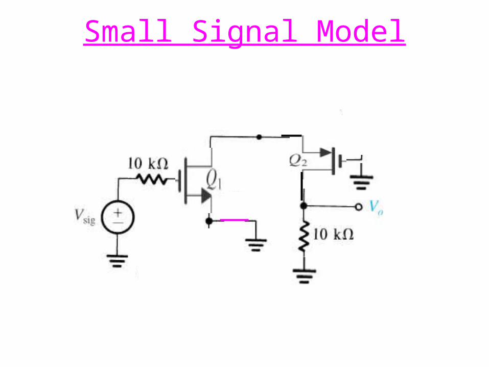
Small Signal Model
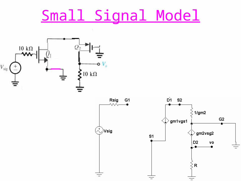
Small Signal Model
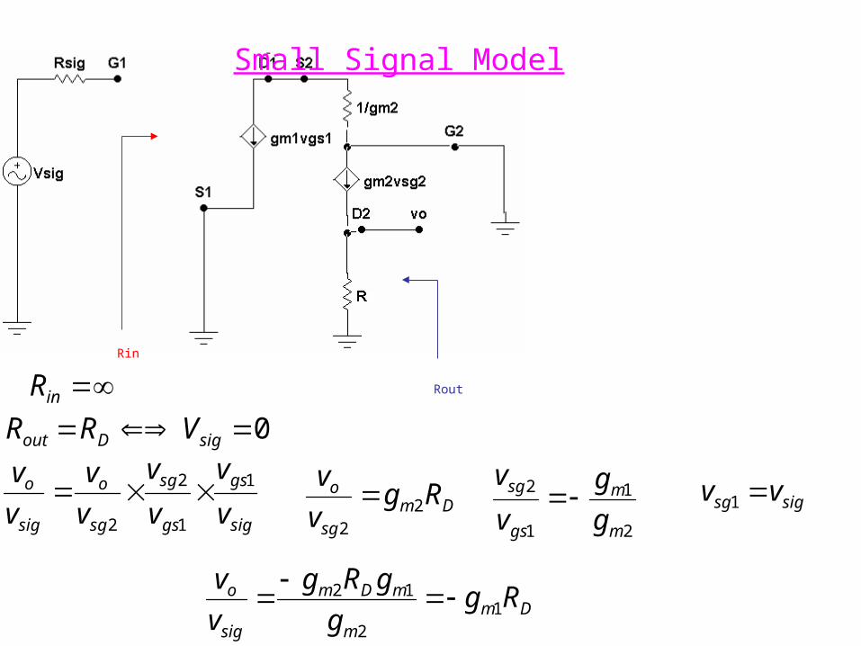
Small Signal Model
Rin
inR Rout
0 sigDout VRR
sigsg vv 1sig
gs
gs
sg
sg
o
sig
o
v
v
v
v
v
v
v
v 1
1
2
2
2
1
1
2
m
m
gs
sg
g
g
v
vDm
sg
o Rgv
v2
2
Dmm
mDm
sig
o Rgg
gRg
v
v1
2
12
1rRin
Cout RR
121
rR
R
v
v
sig
C
sig
o
1
inR
Dout RR
Dmsig
o Rgv
v1
11
2
1
m
sig
C
sig
o
g
RR
v
v

Problem 6-127(f)
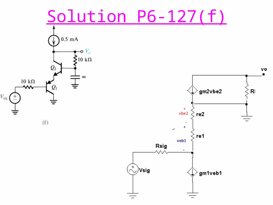
Solution P6-127(f)
+
+
-
-
vbe2
veb1
+
+
-
-
vbe2
veb1
+
vi
-
Solution P6-127(f)))(1( 211
1
1ee
b
bin rr
i
vR
Lout RR
sig
i
i
be
be
O
sig
O
v
v
v
v
v
v
v
v 2
2
21
22
ee
e
i
be
rr
r
v
v
sigee
ee
sigin
in
sig
i
Rrr
rr
RR
R
v
v
))(1(
))(1(
211
211
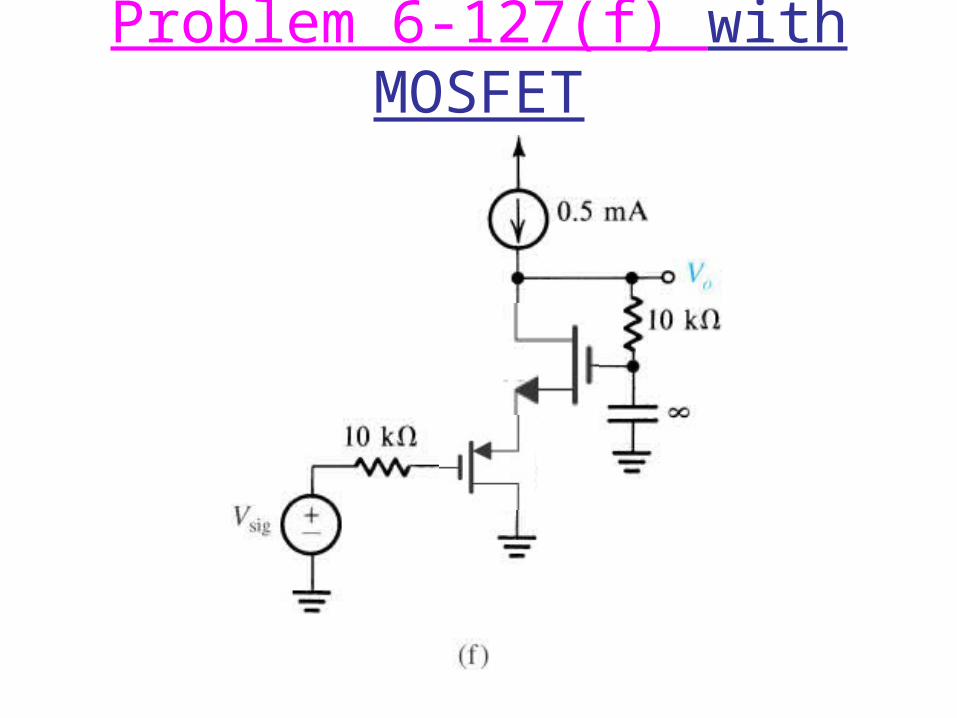
Problem 6-127(f) with MOSFET
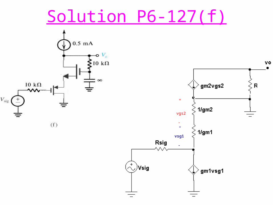
-
-
vgs2
vsg1
+
+
Solution P6-127(f)

-
-
vgs2
vsg1
+
+
Solution P6-127(f)
+vi
-
1g
iin i
vR
sig
i
i
gs
gs
O
sig
O
v
v
v
v
v
v
v
v 2
2
21
1
21
22
11
1
mm
m
mm
m
i
gs
gg
g
gg
g
v
v
sigi vv
ig1=0
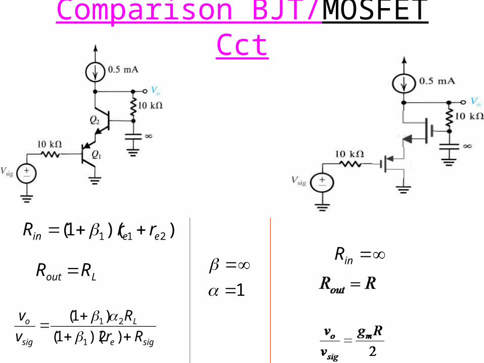
Comparison BJT/MOSFET Cct
inR))(1( 211 eein rrR
Lout RR
sige
L
sig
o
Rr
R
v
v
)2)(1(
)1(
1
21
1
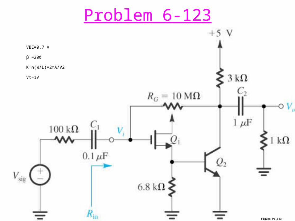
Figure P6.123
Problem 6-123
VBE=0.7 V
β =200
K’n(W/L)=2mA/V2
Vt=1V
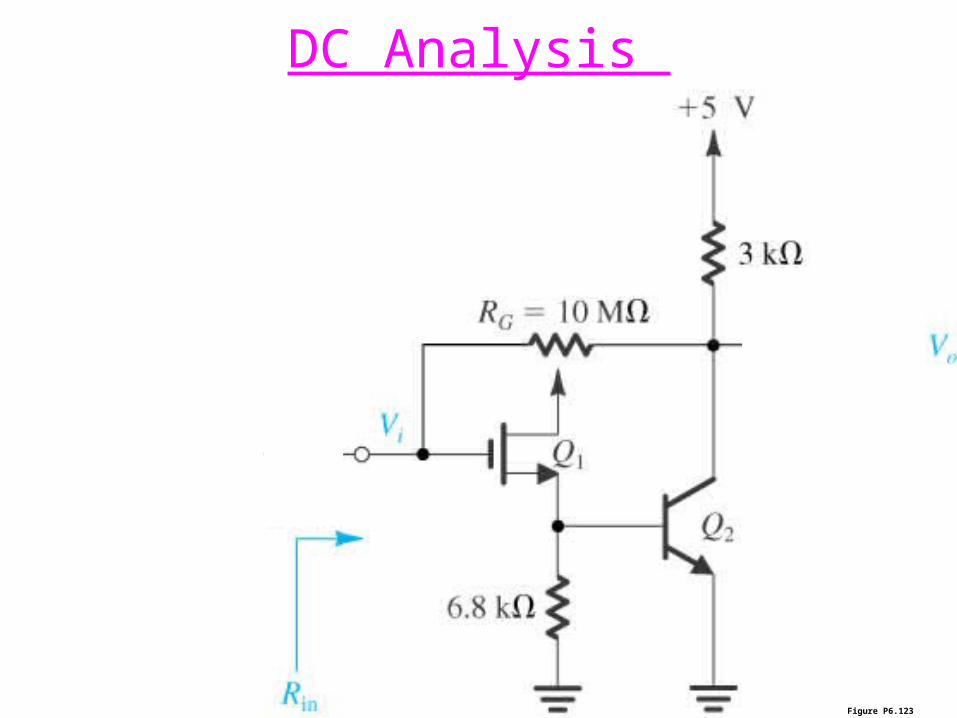
Figure P6.123
DC Analysis
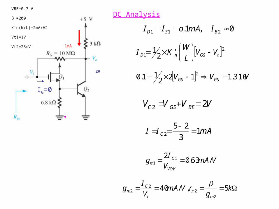
DC AnalysisVBE=0.7 V
β =200
K’n(W/L)=2mA/V2
Vt1=1V
Vt2=25mV
0.7V
I=0.7/6.8=0.1mA
0 ,1. 211 BSD ImAoII
VVV GSGS 316.112211.0 2
21 '2
1tGSnD VV
L
WKI
IG=0
2V
VVVV BEGSC 22
1mA
mAII C 13
252
VmAV
Ig
VOV
Dm /63.0
2 11
kg
rVmAV
Ig
mt
Cm 5,/40
22
22

Small Signal Model
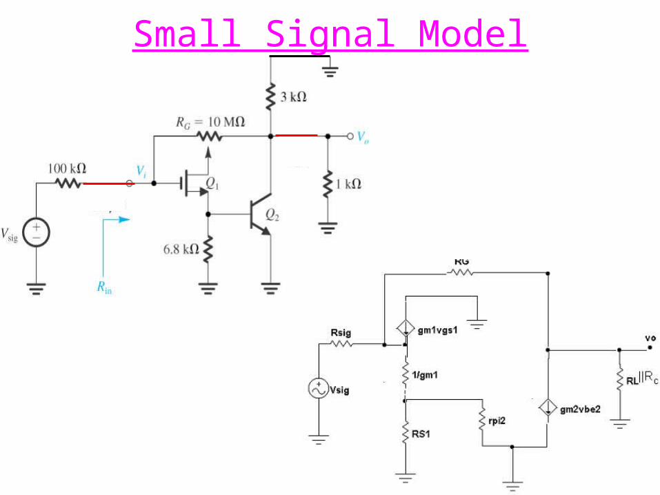
Small Signal Model
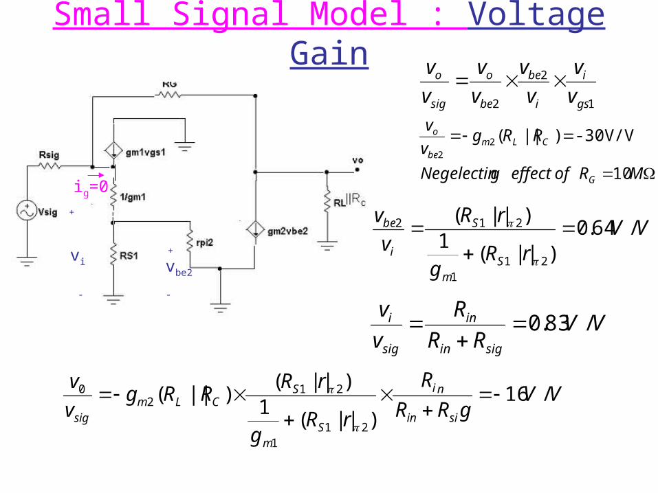
Small Signal Model : Voltage Gain
ig=0
+
vi
-
+
vbe2
-
1
2
2 gs
i
i
be
be
o
sig
o
v
v
v
v
v
v
v
v
MRofeffectgNegelectin
RRgv
v
G
C Lmbe
o
10
-30V/V )||(22
VVrR
g
rR
v
v
Sm
S
i
be /64.0)||(
1)||(
211
212
VVRR
R
v
v
sigin
in
sig
i /83.0
VVgRR
R
rRg
rRRRg
v
v
siin
ni
Sm
SCLm
sig
/16)||(
1)||(
)||(
211
212
0
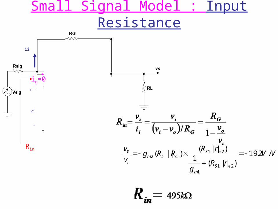
Small Signal Model : Input Resistance
Rin
+
vi
-
ii
VVrR
g
rRRRg
v
v
Sm
SCLm
i
/2.19)||(
1)||(
)||(
211
212
0
ig=0
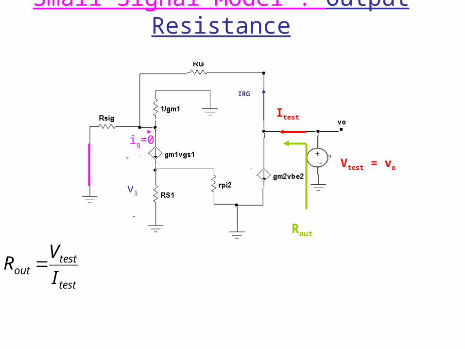
ig=0
+
vi
-
Rout
Vtest = vo
Itest
test
testout I
VR
IRG
Small Signal Model : Output Resistance
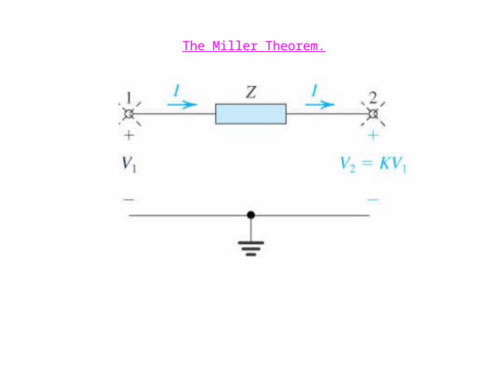
The Miller Theorem.
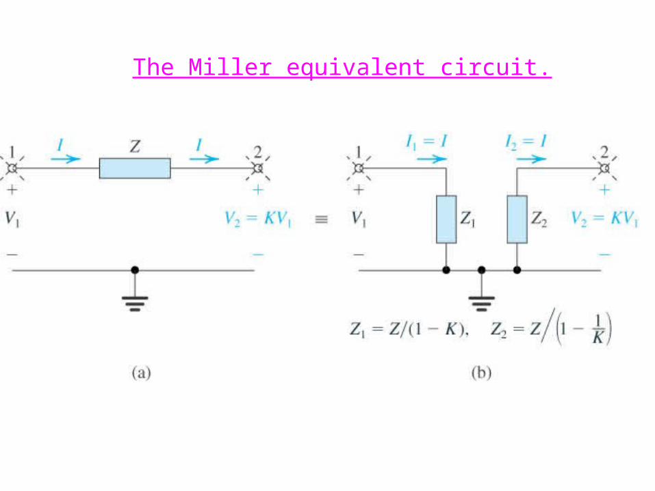
The Miller equivalent circuit.
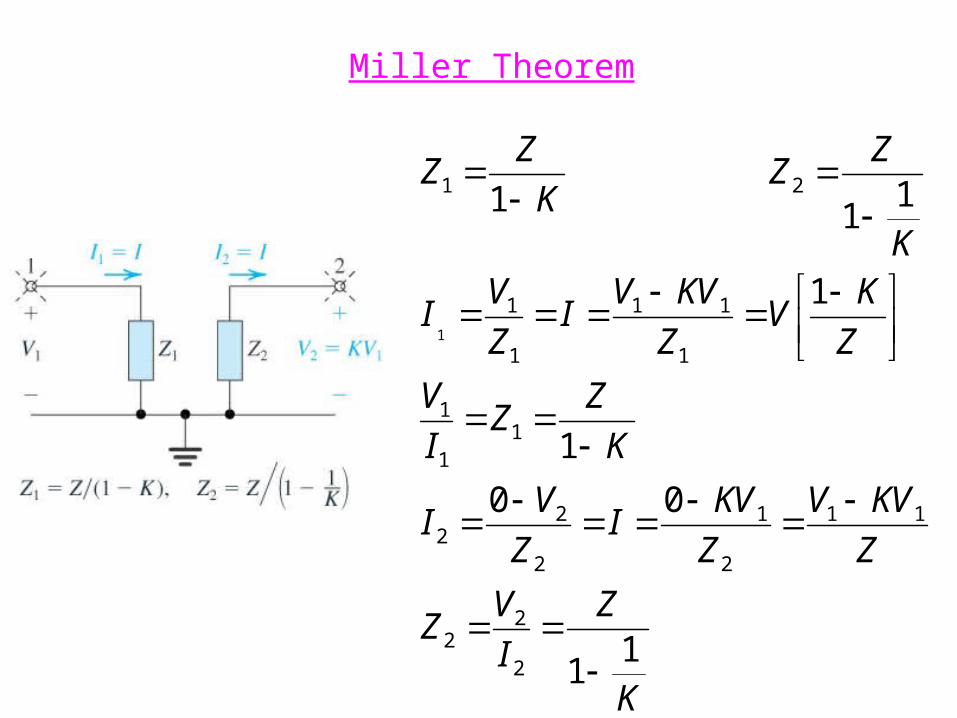
K
Z
I
VZ
Z
KVV
Z
KVI
Z
VI
K
ZZ
I
V
Z
KV
Z
KVVI
Z
VI
K
ZZ
K
ZZ
11
00
1
1
11
1
2
22
11
2
1
2
22
11
1
1
11
1
1
21
1
Miller Theorem
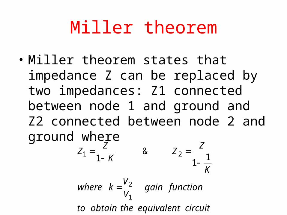
Miller theorem
• Miller theorem states that impedance Z can be replaced by two impedances: Z1 connected between node 1 and ground and Z2 connected between node 2 and ground where
circuitequivalenttheobtainto
functiongainV
Vkwhere
K
ZZ
K
ZZ
11
& 1
1
2
21

• Miller equivalent circuit is valid only as long as the rest of the circuit remains unchanged
• Miller equivalent circuit cannot be used directly to determine the output resistance of an amplifier. It is due to the fact for output impedance test source is required and thus circuit has a major change.
Miller theorem
Circuit for Example 6.7.
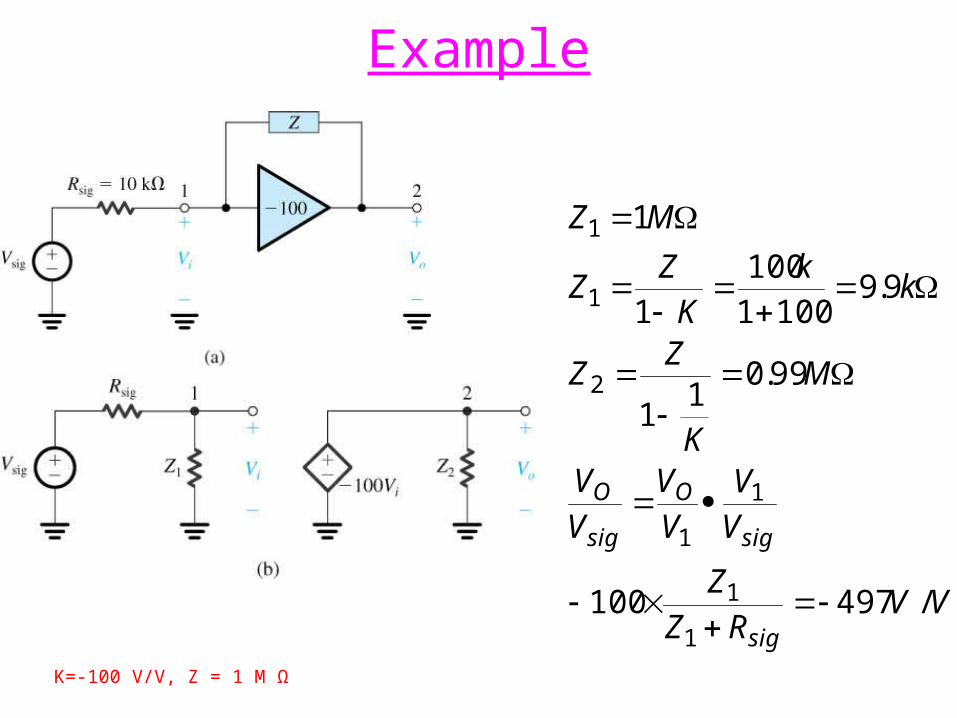
Example
VVRZ
Z
V
V
V
V
V
V
M
K
ZZ
kk
K
ZZ
MZ
sig
sig
O
sig
O
/ 497100
99.01
1
9.91001
100
1
1
1
1
1
1
2
1
1
K=-100 V/V, Z = 1 M Ω
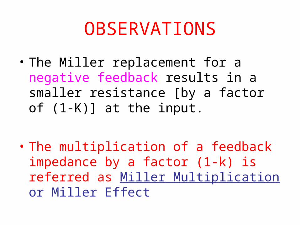
OBSERVATIONS
• The Miller replacement for a negative feedback results in a smaller resistance [by a factor of (1-K)] at the input.
• The multiplication of a feedback impedance by a factor (1-k) is referred as Miller Multiplication or Miller Effect

Small Signal ModelCE with RE includng r0
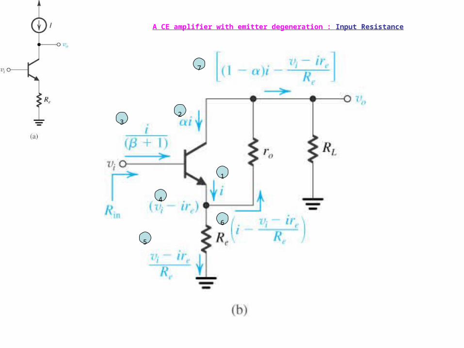
A CE amplifier with emitter degeneration : Input Resistance
1
23
4
5
6
7
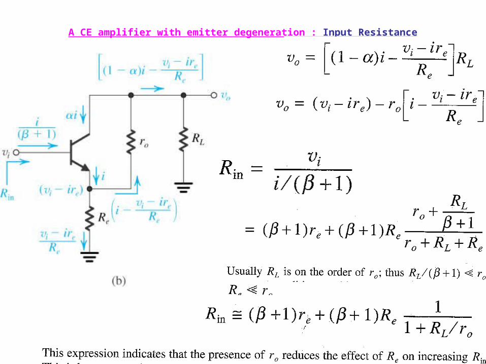
A CE amplifier with emitter degeneration : Input Resistance
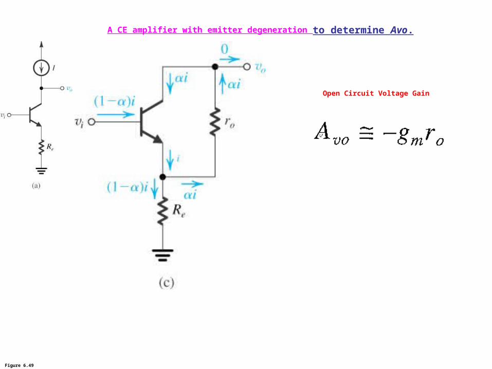
Figure 6.49
A CE amplifier with emitter degeneration to determine Avo.
Open Circuit Voltage Gain
A CE amplifier with emitter degeneration
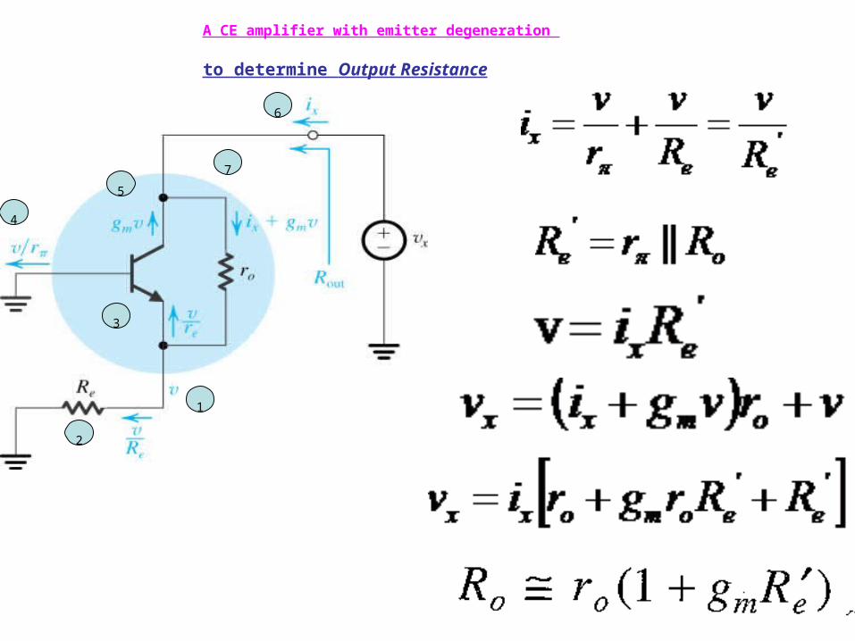
to determine Output Resistance
1
2
3
4
5
6
7
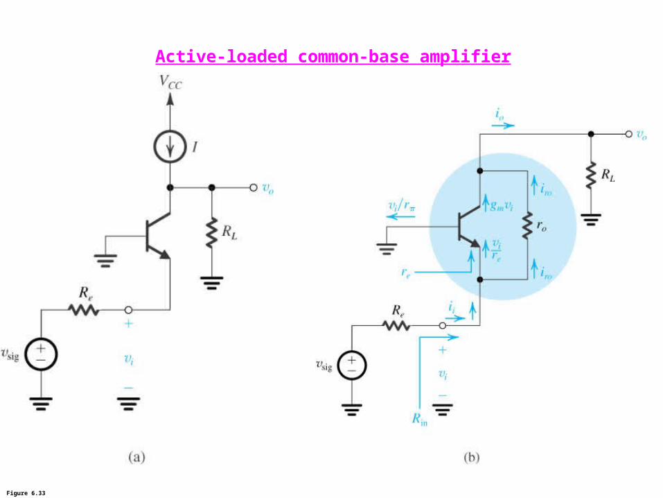
Figure 6.33
Active-loaded common-base amplifier
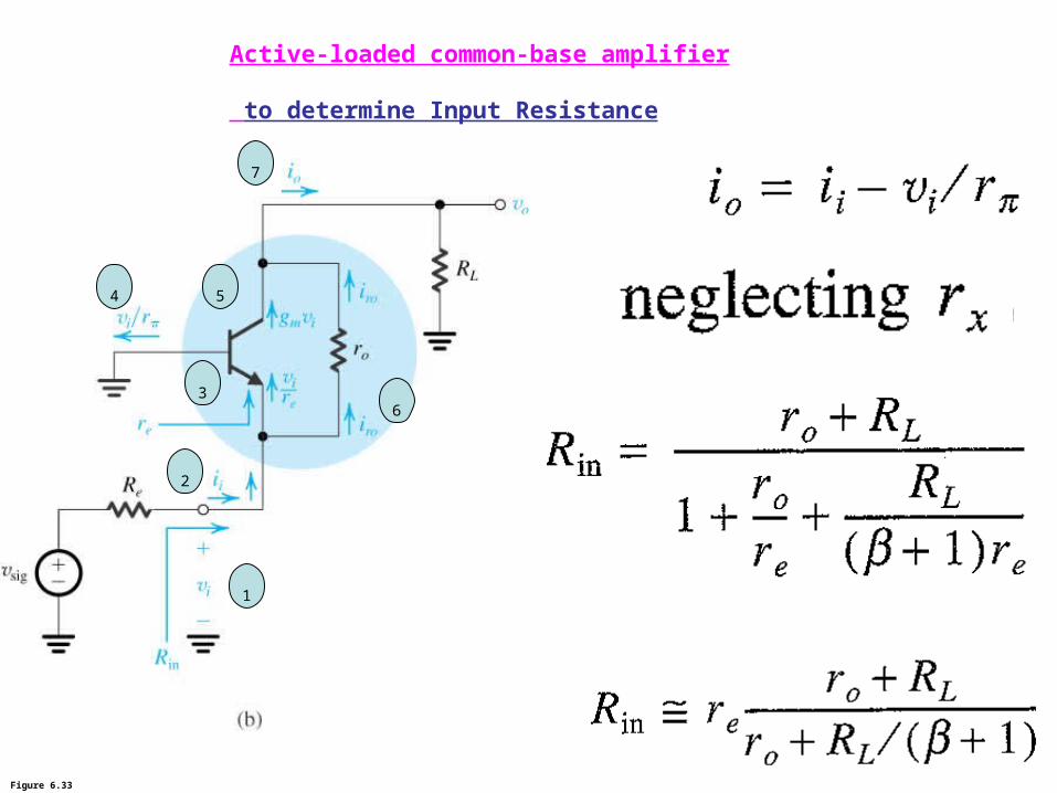
Figure 6.33
Active-loaded common-base amplifier
to determine Input Resistance
1
2
3
4 5
6
7
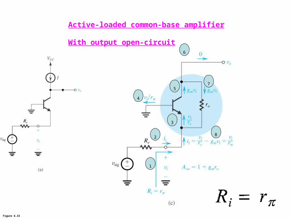
Figure 6.33
Active-loaded common-base amplifier
With output open-circuit
1
28
3
4
5
6
7
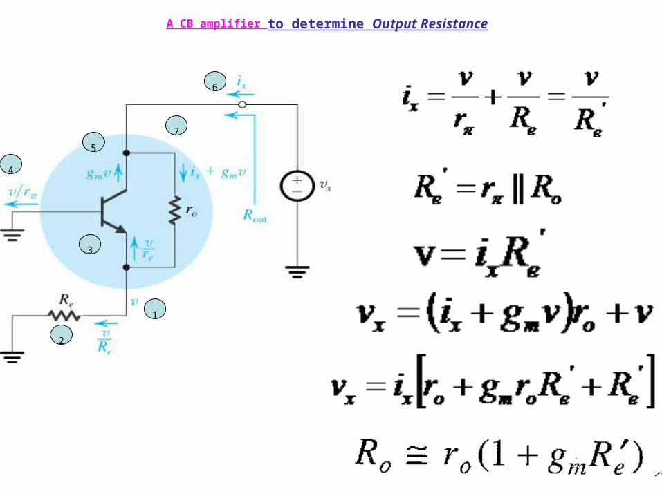
A CB amplifier to determine Output Resistance
1
2
3
4
5
6
7
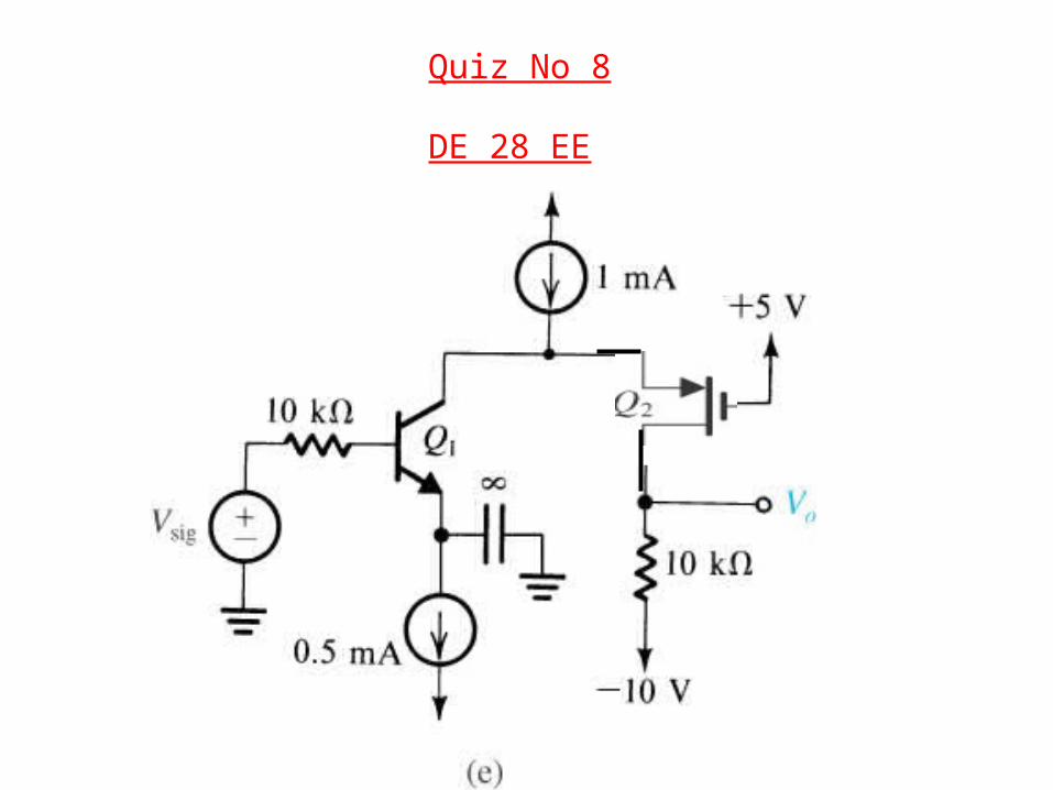
Quiz No 8
DE 28 EE

Quiz No 8
DE 28 EE