lecture 6: junction characterisation
TRANSCRIPT

Lecture 6 Junction characterisation
Jon Major
Nov 6th 2014
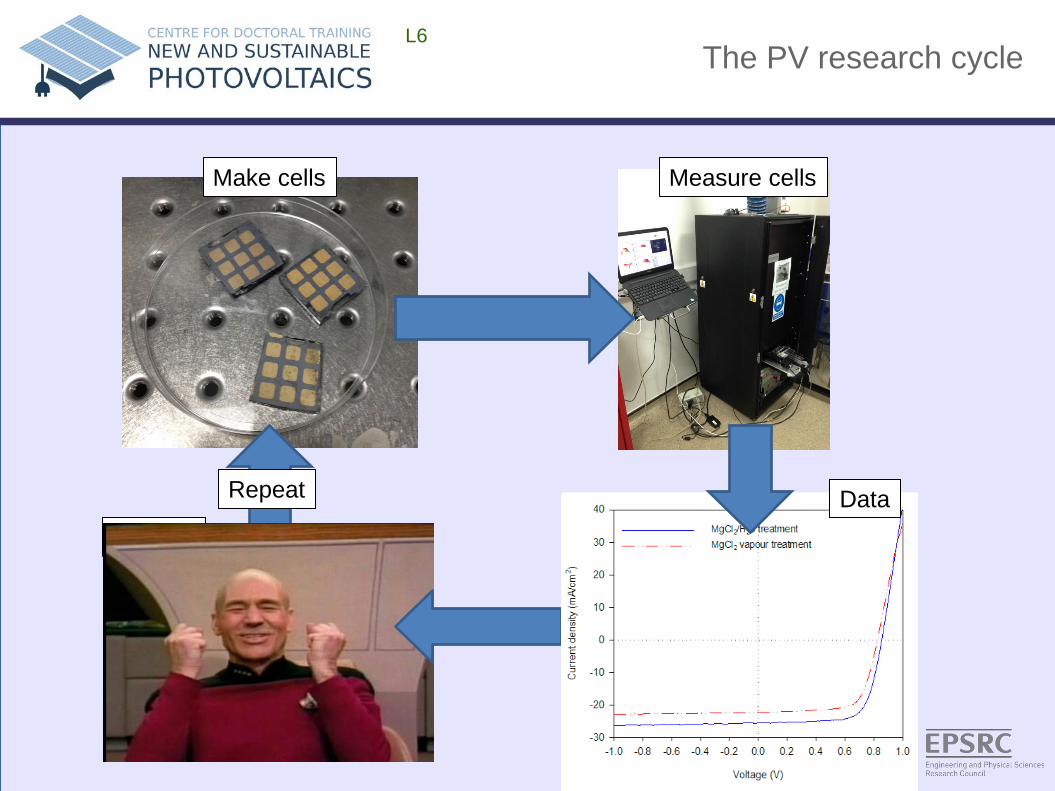
The PV research cycle L6
Voltage (V)
-1.0 -0.5 0.0 0.5 1.0
Cur
rent
den
sity
(mA
/cm
2 )
-20
0
20
40
1.1%4.9%
Make cells Measure cells
Despair
Repeat Data

Lecture Outline LX
• Analysis of current voltage (J-V) curves
• External quantum efficiency (EQE) measurements
• Capacitance voltage (C-V) measurements
Key junction characterisation techniques
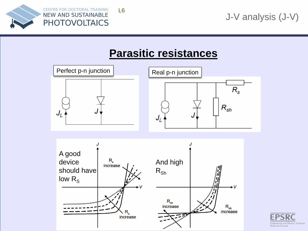
J-V analysis (J-V) L6
Parasitic resistances Perfect p-n junction Real p-n junction
A good device should have low RS
And high RSh
J-V analysis (J-V) L6
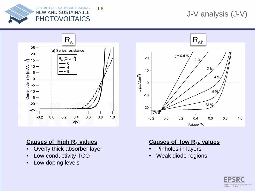
Rs Rsh
Causes of high RS values • Overly thick absorber layer • Low conductivity TCO • Low doping levels
Causes of low RSh values • Pinholes in layers • Weak diode regions
J-V analysis (J-V) L6
J-V analysis (J-V) L6
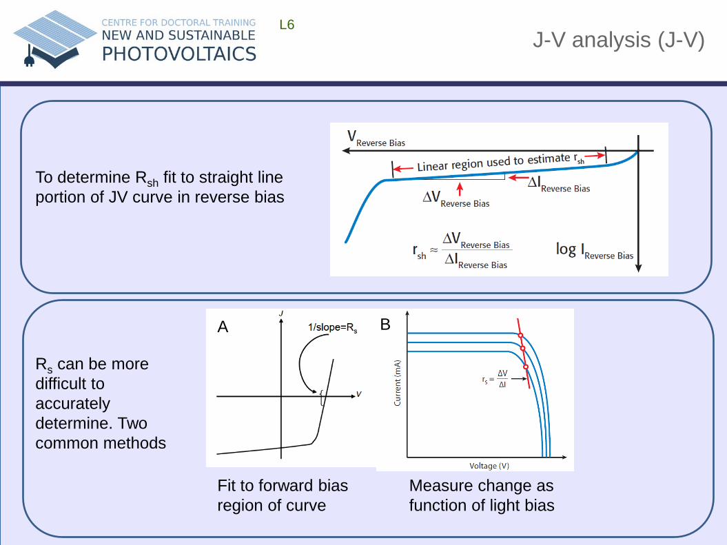
To determine Rsh fit to straight line portion of JV curve in reverse bias
Rs can be more difficult to accurately determine. Two common methods
Fit to forward bias region of curve
Measure change as function of light bias
A B
J-V analysis (J-V) L6
“Roll-over”
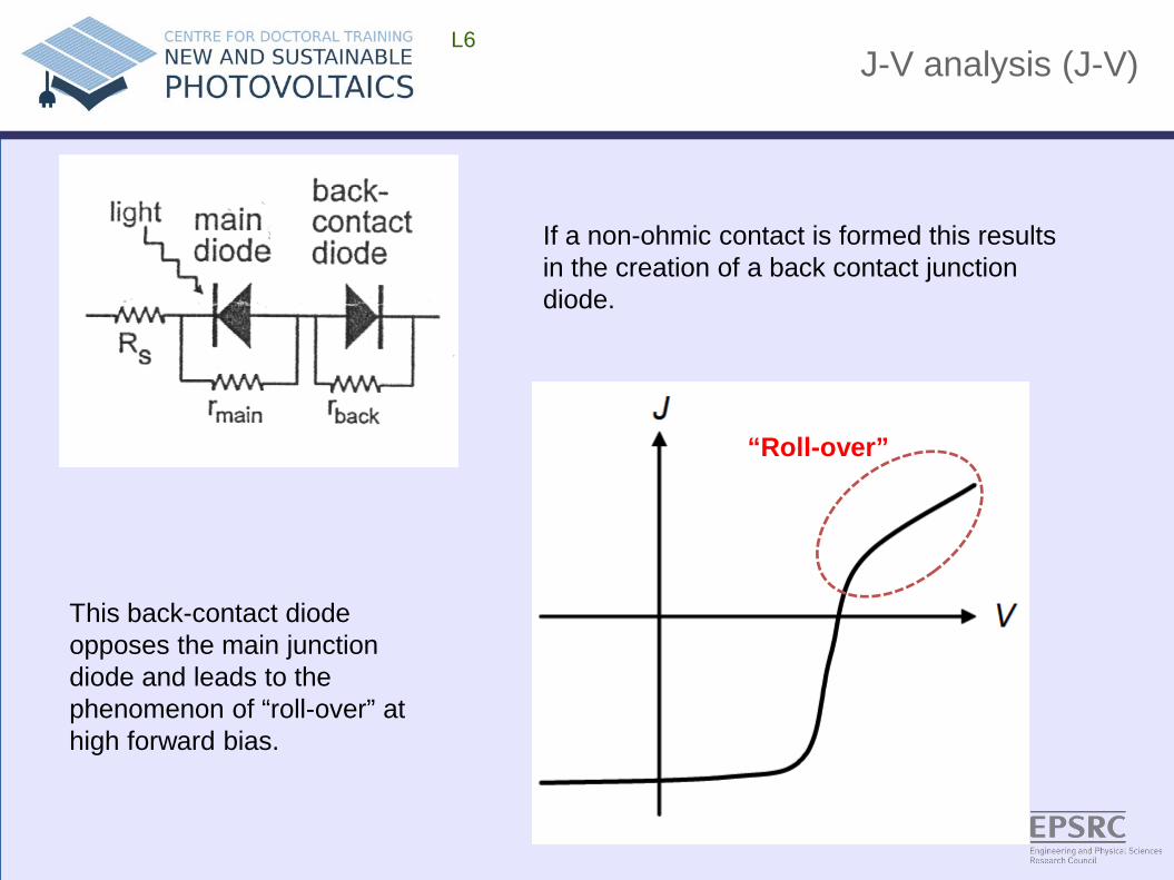
If a non-ohmic contact is formed this results in the creation of a back contact junction diode.
This back-contact diode opposes the main junction diode and leads to the phenomenon of “roll-over” at high forward bias.
J-V analysis (J-V) L6
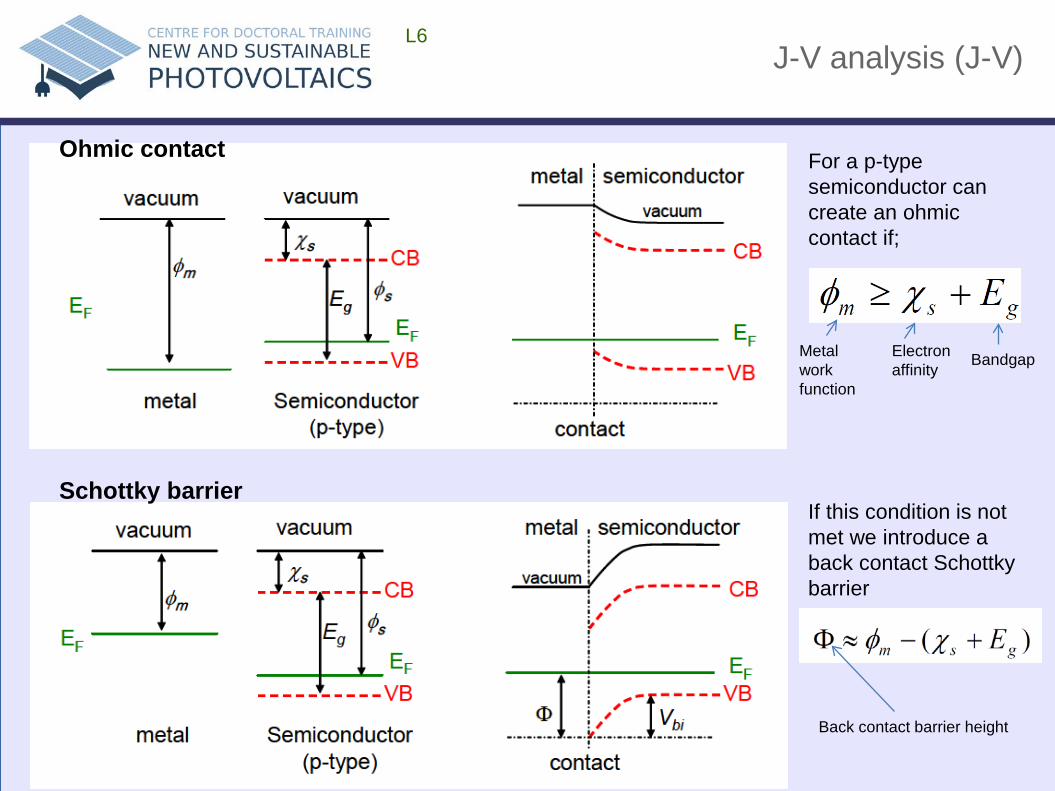
For a p-type semiconductor can create an ohmic contact if;
Schottky barrier
Ohmic contact
If this condition is not met we introduce a back contact Schottky barrier
Electron affinity Bandgap Metal
work function
Back contact barrier height
J-V-T analysis L6
-0.5 0.0 0.5 1.0 1.5
-40
-20
0
20
40
60
80
100
120
140
303 K
293 K
283 K
333 K
313 K323 K
273 K
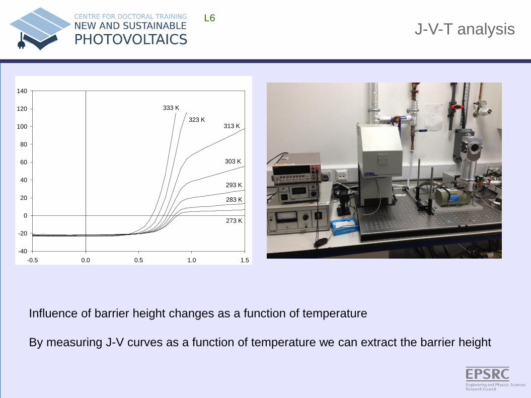
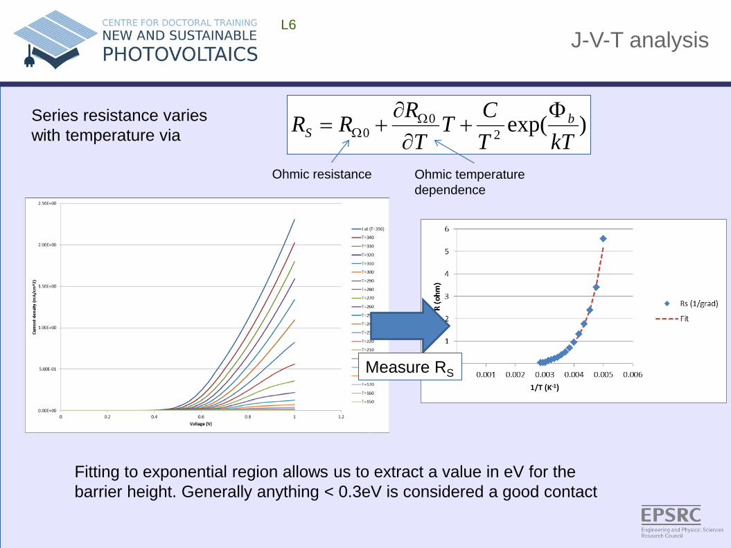
Influence of barrier height changes as a function of temperature By measuring J-V curves as a function of temperature we can extract the barrier height
J-V-T analysis L6
Fitting to exponential region allows us to extract a value in eV for the barrier height. Generally anything < 0.3eV is considered a good contact
)exp(20
0 kTTCT
TRRR b
SΦ
+∂∂
+= ΩΩ
Measure RS
Series resistance varies with temperature via
Ohmic resistance Ohmic temperature dependence

A cautionary tale L6
Errors in J-V analysis (J-V) L6
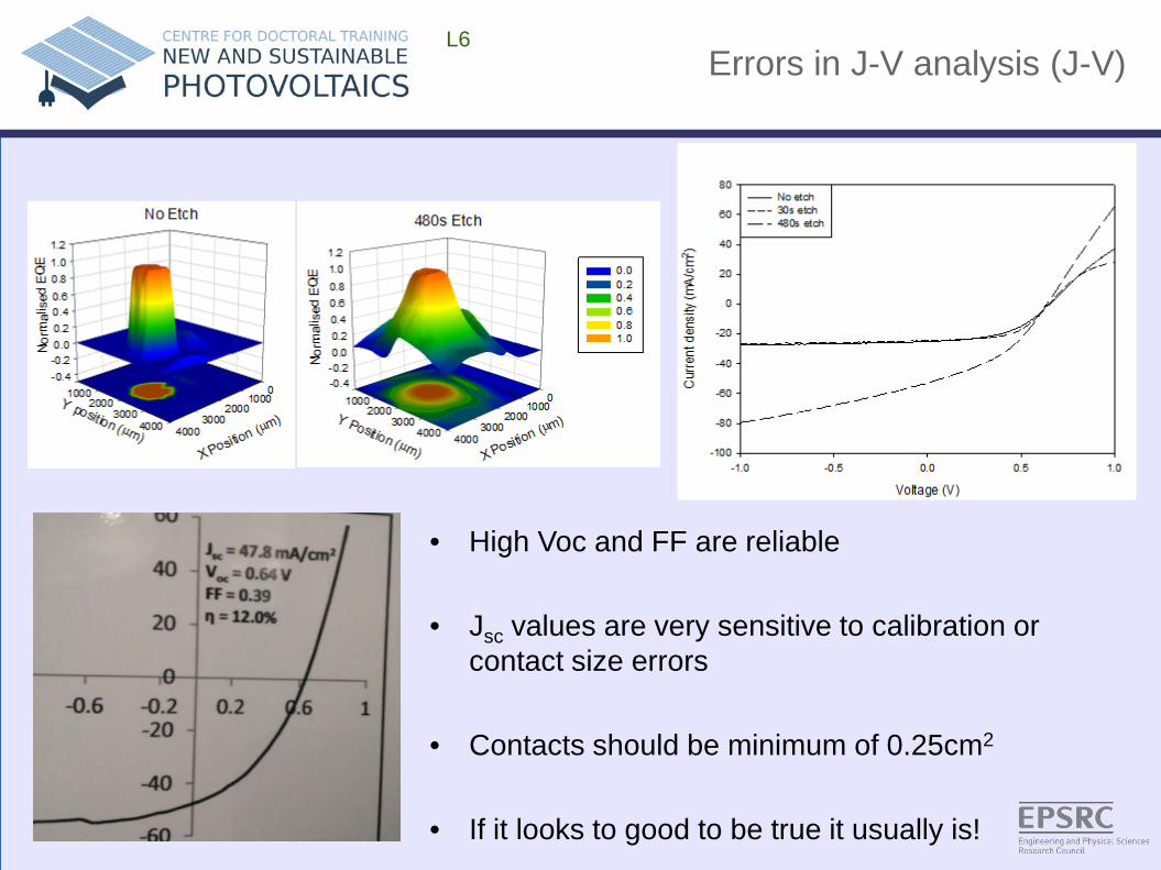
• High Voc and FF are reliable
• Jsc values are very sensitive to calibration or contact size errors
• Contacts should be minimum of 0.25cm2
• If it looks to good to be true it usually is!
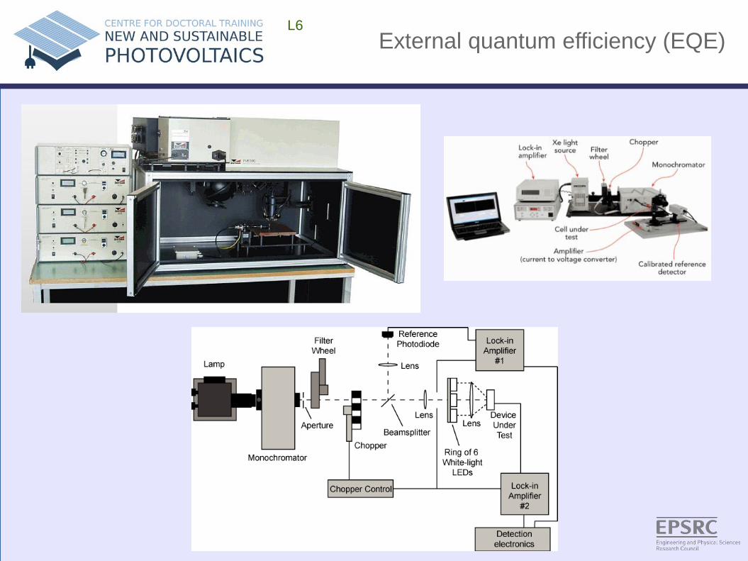
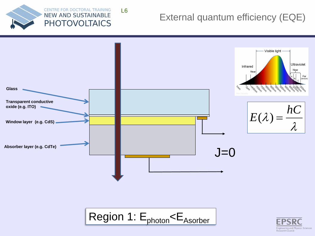
External quantum efficiency (EQE) L6
External quantum efficiency (EQE) L6
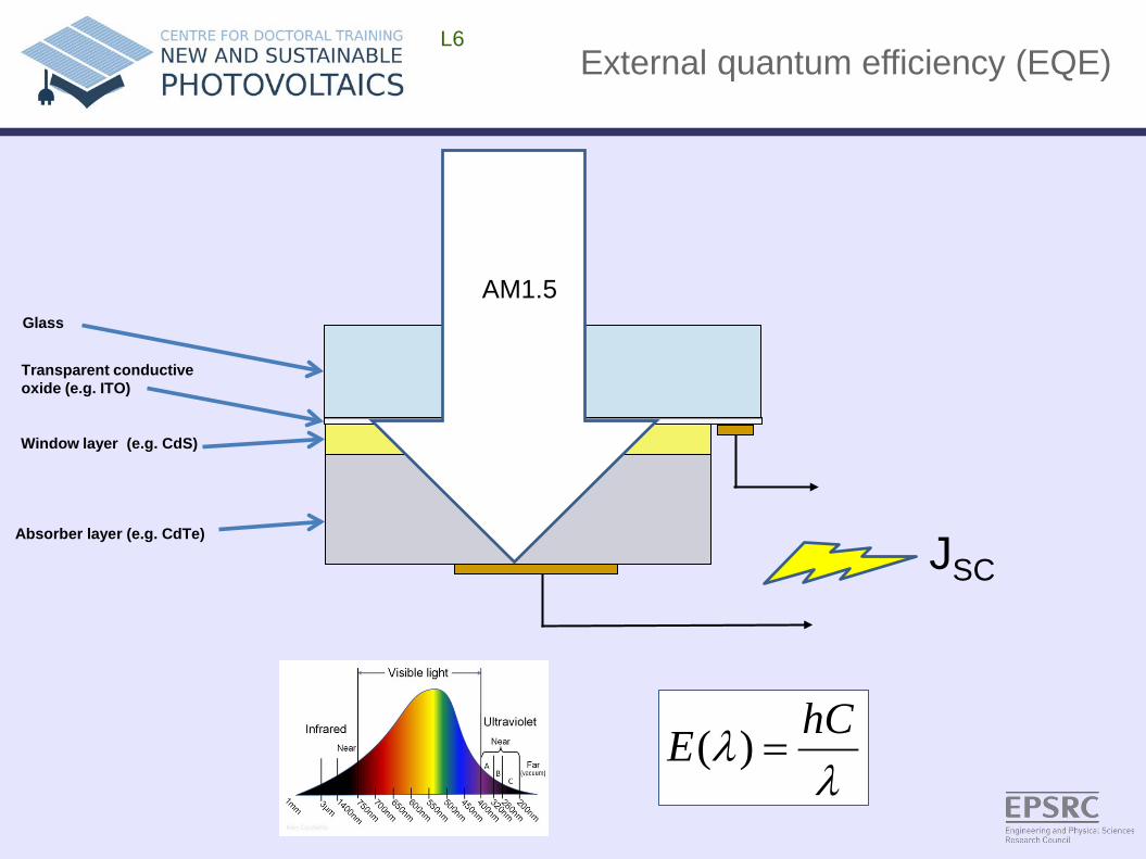
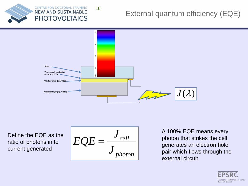
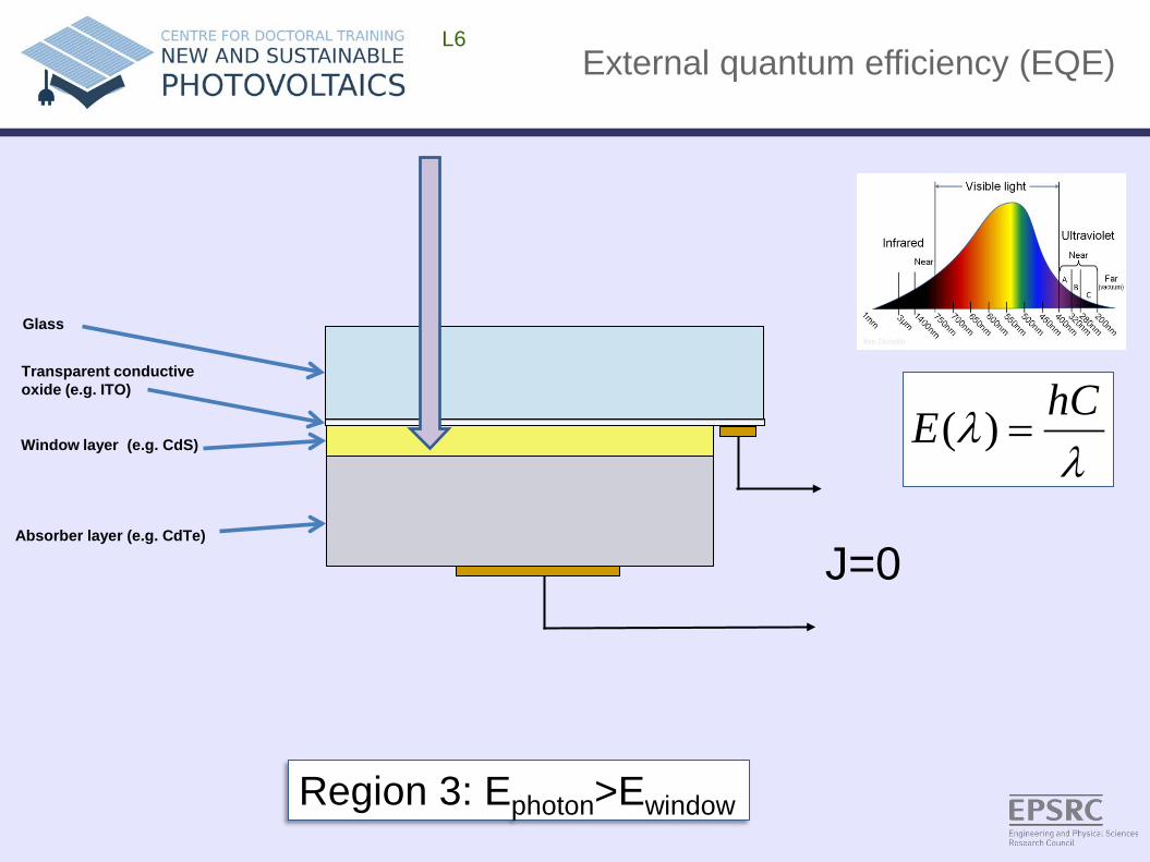
Absorber layer (e.g. CdTe)
Window layer (e.g. CdS)
Glass
Transparent conductive oxide (e.g. ITO)
λλ hCE =)(
AM1.5 AM1.5
JSC
External quantum efficiency (EQE) L6
)(λJ
photon
cell
JJEQE =
Define the EQE as the ratio of photons in to current generated
A 100% EQE means every photon that strikes the cell generates an electron hole pair which flows through the external circuit
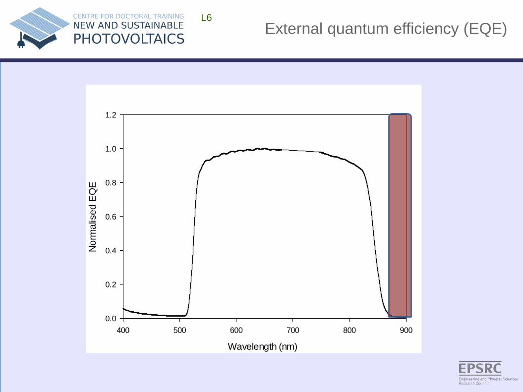
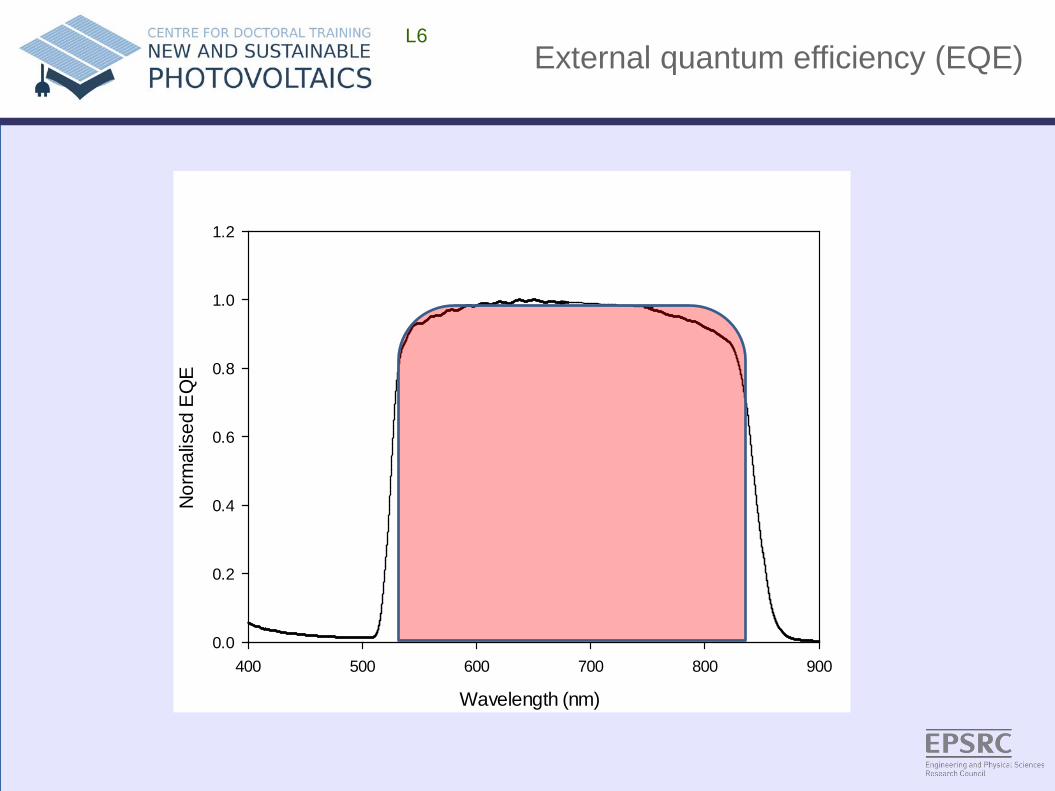
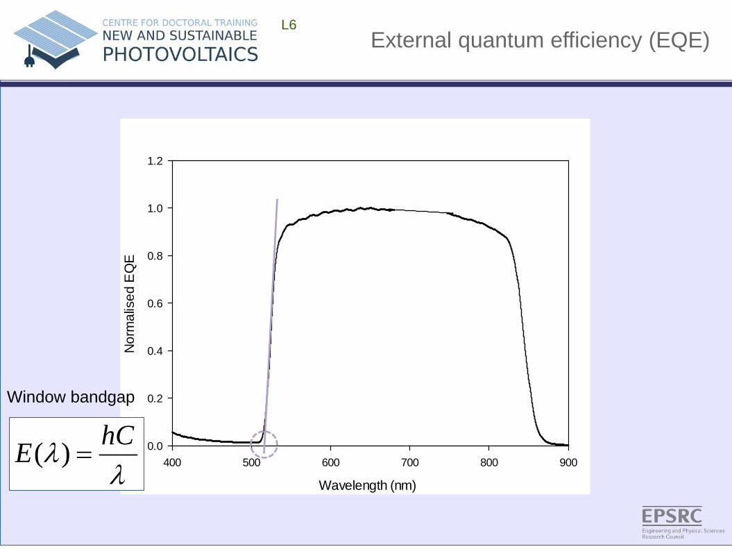
External quantum efficiency (EQE) L6
Wavelength (nm)
400 500 600 700 800 900
Nor
mal
ised
EQ
E
0.0
0.2
0.4
0.6
0.8
1.0
1.2
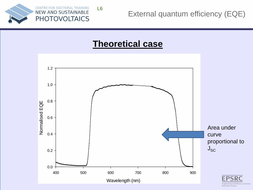
Theoretical case
Area under curve proportional to JSC
External quantum efficiency (EQE) L6
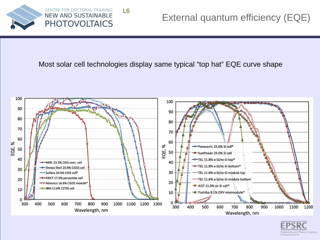
Most solar cell technologies display same typical “top hat” EQE curve shape
External quantum efficiency (EQE) L6
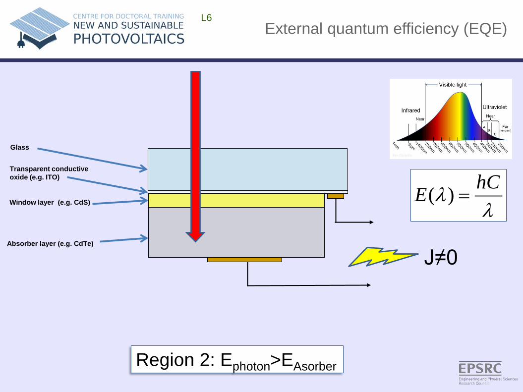
External quantum efficiency (EQE) L6
Absorber layer (e.g. CdTe)
Window layer (e.g. CdS)
Glass
Transparent conductive oxide (e.g. ITO)
λλ hCE =)(
J=0
Region 1: Ephoton<EAsorber
External quantum efficiency (EQE) L6
Wavelength (nm)
400 500 600 700 800 900
Nor
mal
ised
EQ
E
0.0
0.2
0.4
0.6
0.8
1.0
1.2
External quantum efficiency (EQE) L6
Absorber layer (e.g. CdTe)
Window layer (e.g. CdS)
Glass
Transparent conductive oxide (e.g. ITO)
λλ hCE =)(
J≠0
Region 2: Ephoton>EAsorber
External quantum efficiency (EQE) L6
Wavelength (nm)
400 500 600 700 800 900
Nor
mal
ised
EQ
E
0.0
0.2
0.4
0.6
0.8
1.0
1.2

External quantum efficiency (EQE) L6
Wavelength (nm)
400 500 600 700 800 900
Nor
mal
ised
EQ
E
0.0
0.2
0.4
0.6
0.8
1.0
1.2
Absorber bandgap
λλ hCE =)(
External quantum efficiency (EQE) L6
Absorber layer (e.g. CdTe)
Window layer (e.g. CdS)
Glass
Transparent conductive oxide (e.g. ITO)
λλ hCE =)(
J=0
Region 3: Ephoton>Ewindow

External quantum efficiency (EQE) L6
Wavelength (nm)
400 500 600 700 800 900
Nor
mal
ised
EQ
E
0.0
0.2
0.4
0.6
0.8
1.0
1.2
External quantum efficiency (EQE) L6
Wavelength (nm)
400 500 600 700 800 900
Nor
mal
ised
EQ
E
0.0
0.2
0.4
0.6
0.8
1.0
1.2
Window bandgap
λλ hCE =)(
External quantum efficiency (EQE) L6
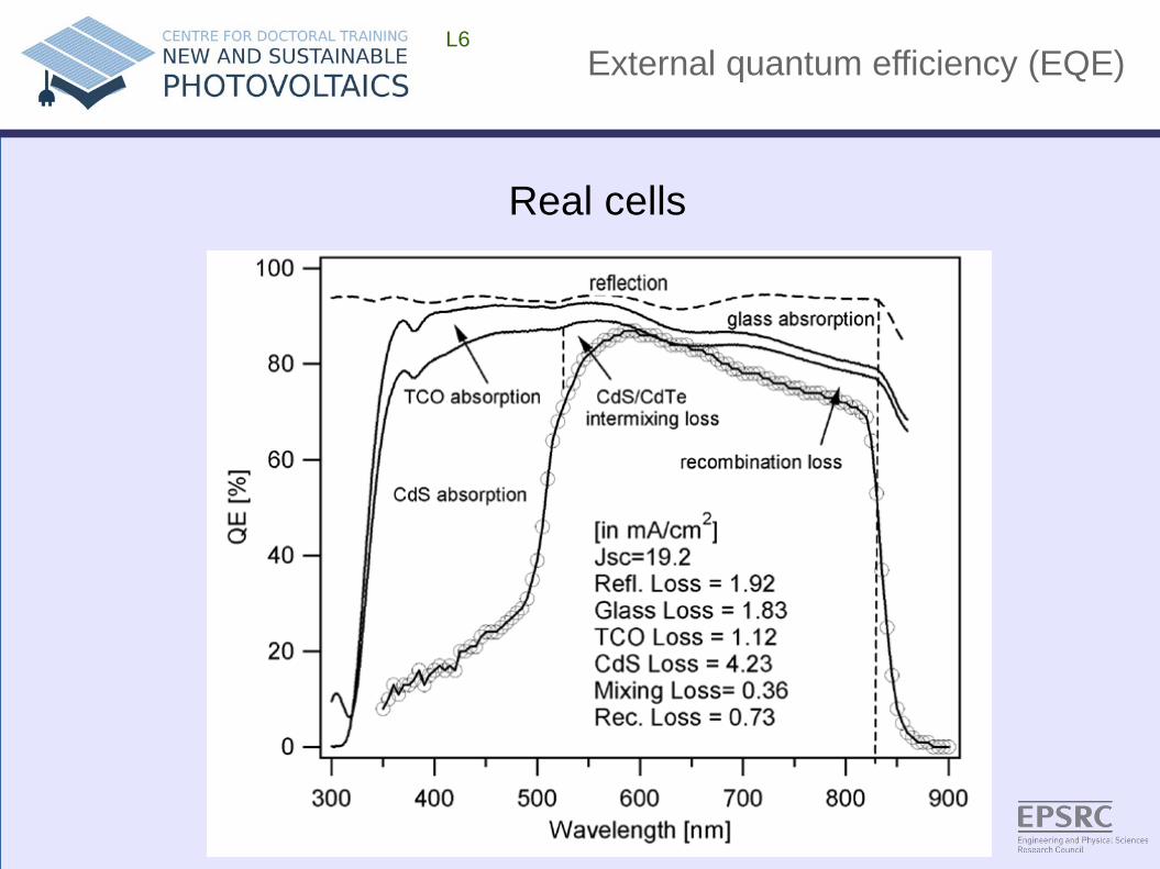
Real cells
External quantum efficiency (EQE) L6
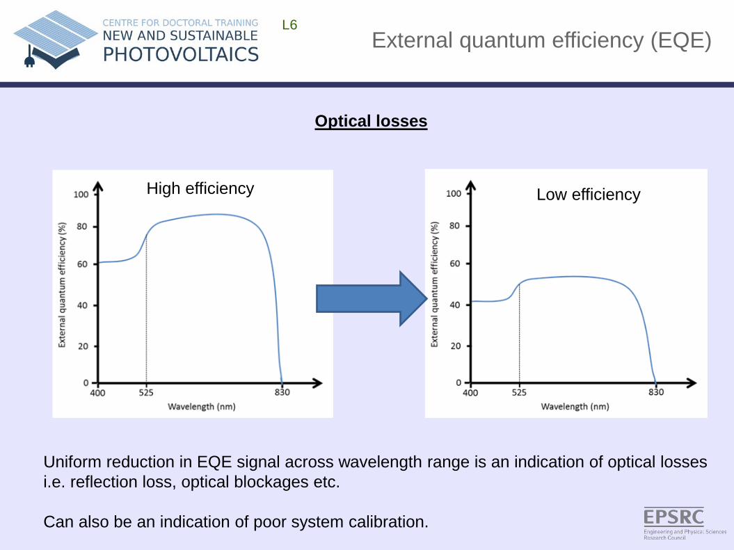
Optical losses
Uniform reduction in EQE signal across wavelength range is an indication of optical losses i.e. reflection loss, optical blockages etc. Can also be an indication of poor system calibration.
High efficiency Low efficiency

External quantum efficiency (EQE) L6
Wavelength (nm)
400 500 600 700 800 900
Nor
mal
ised
EQ
E
0.0
0.2
0.4
0.6
0.8
1.0
1.2300nm CdS250nm CdS200nm CdS
window/ n-type layer losses
Reduced window layer thickness allows more light transmission to absorber
Higher bandgap n-type layer shifts absorption edge
High efficiency
Lower efficiency
High efficiency
Lower efficiency

External quantum efficiency (EQE) L6
If absorber layer is thin or depletion width is narrow then longer wavelength photons have an increased probability of not contributing to photocurrent. See a decrease in EQE for longer wavelengths.
Deep penetration losses
External quantum efficiency (EQE) L6
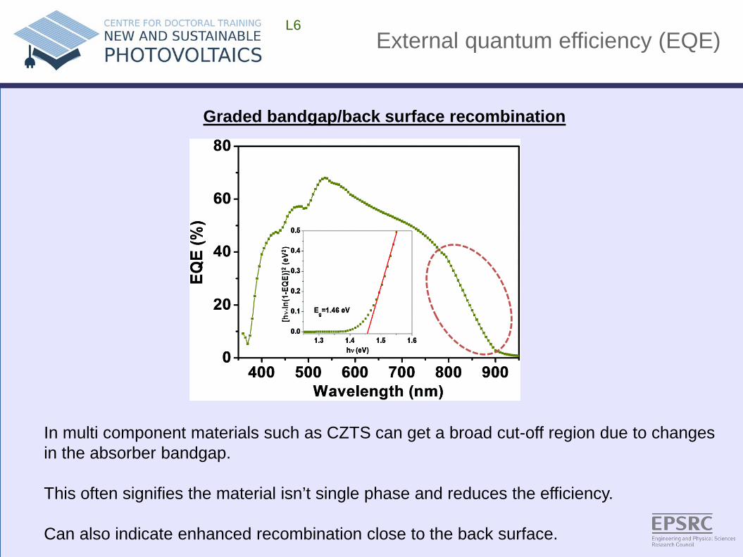
In multi component materials such as CZTS can get a broad cut-off region due to changes in the absorber bandgap. This often signifies the material isn’t single phase and reduces the efficiency. Can also indicate enhanced recombination close to the back surface.
Graded bandgap/back surface recombination
External quantum efficiency (EQE) L6
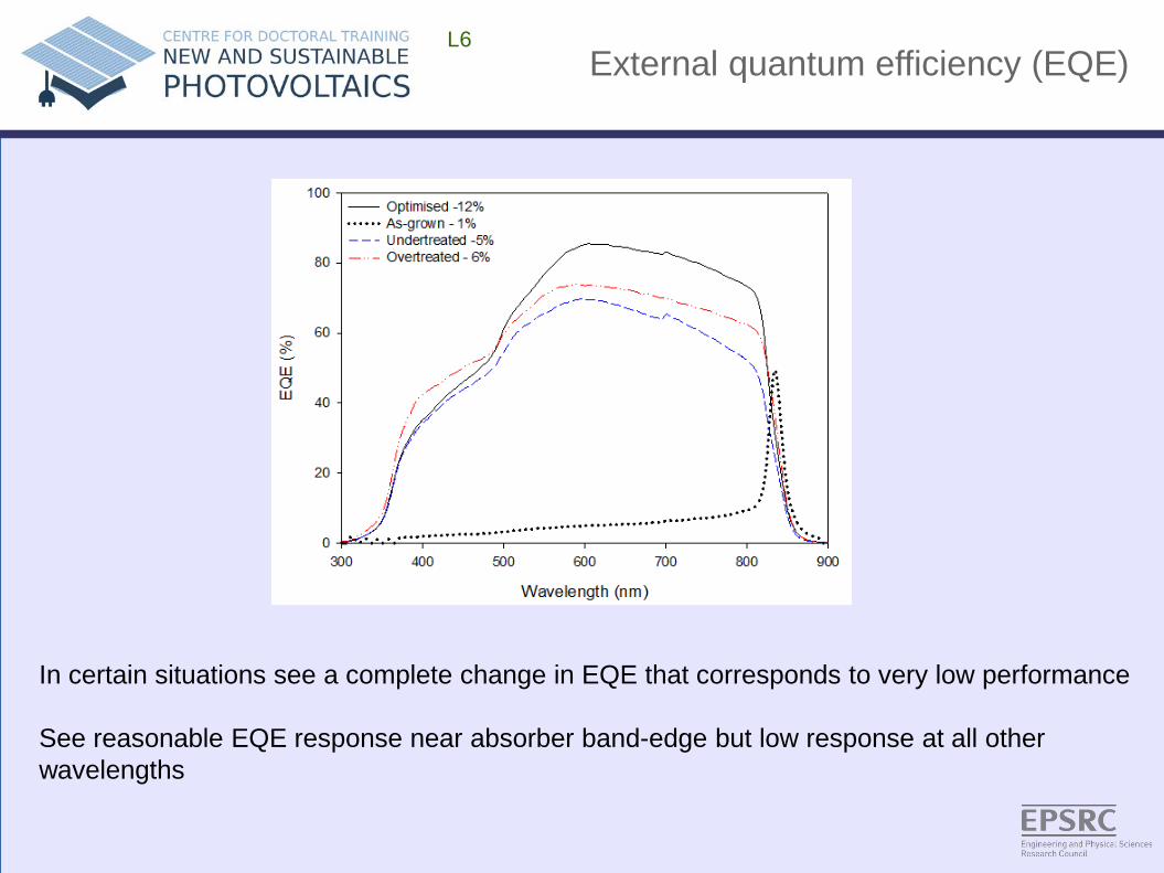
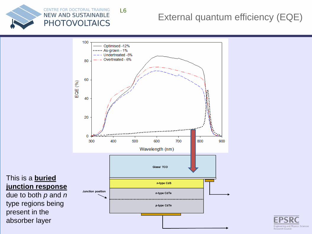
In certain situations see a complete change in EQE that corresponds to very low performance See reasonable EQE response near absorber band-edge but low response at all other wavelengths
External quantum efficiency (EQE) L6
This is a buried junction response due to both p and n type regions being present in the absorber layer
Capacitance Voltage analysis (C-V) L6
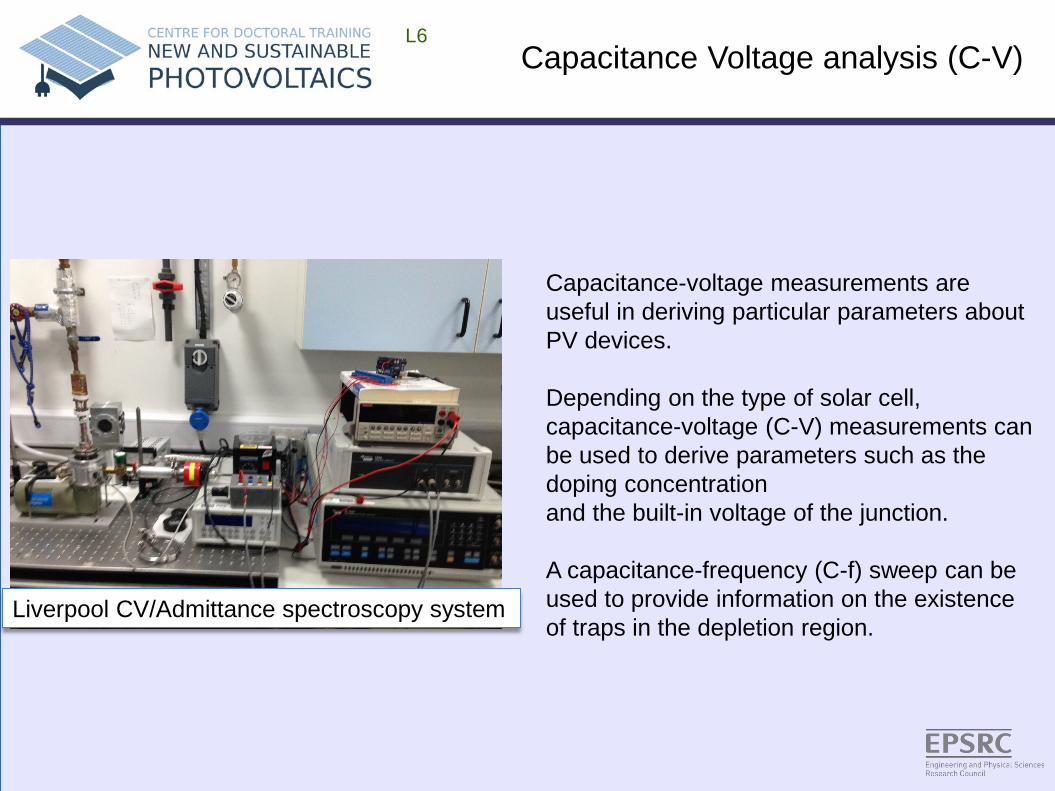
Capacitance-voltage measurements are useful in deriving particular parameters about PV devices. Depending on the type of solar cell, capacitance-voltage (C-V) measurements can be used to derive parameters such as the doping concentration and the built-in voltage of the junction. A capacitance-frequency (C-f) sweep can be used to provide information on the existence of traps in the depletion region.
Liverpool CV/Admittance spectroscopy system
Capacitance Voltage analysis (C-V) L6
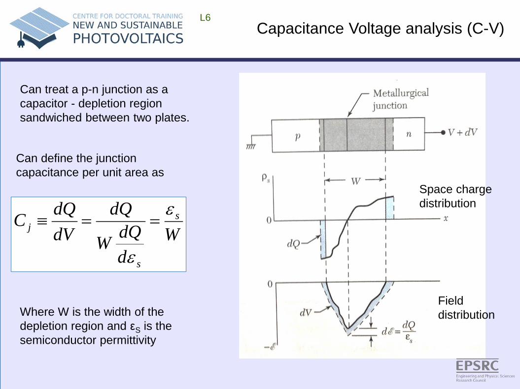
Field distribution
Space charge distribution
WddQW
dQdVdQC s
s
jε
ε
==≡
Can define the junction capacitance per unit area as
Where W is the width of the depletion region and εS is the semiconductor permittivity
Can treat a p-n junction as a capacitor - depletion region sandwiched between two plates.
Capacitance Voltage analysis (C-V) L6
as NqV
C ε21
2 =
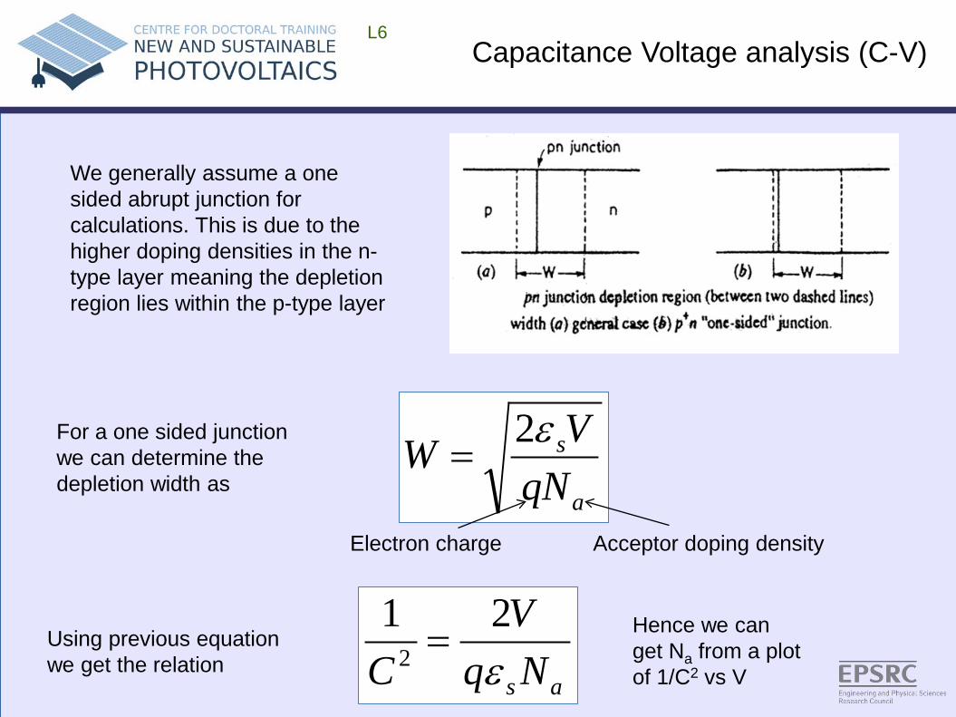
We generally assume a one sided abrupt junction for calculations. This is due to the higher doping densities in the n-type layer meaning the depletion region lies within the p-type layer
a
s
qNVW ε2
=For a one sided junction we can determine the depletion width as
Acceptor doping density Electron charge
Using previous equation we get the relation
Hence we can get Na from a plot of 1/C2 vs V
Capacitance Voltage analysis (C-V) L6
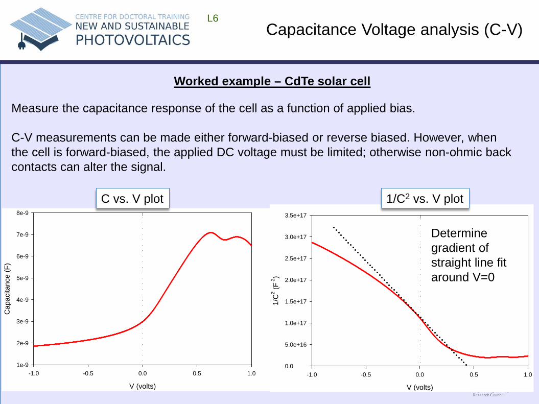
Measure the capacitance response of the cell as a function of applied bias. C-V measurements can be made either forward-biased or reverse biased. However, when the cell is forward-biased, the applied DC voltage must be limited; otherwise non-ohmic back contacts can alter the signal.
V (volts)
-1.0 -0.5 0.0 0.5 1.0
Cap
acita
nce
(F)
1e-9
2e-9
3e-9
4e-9
5e-9
6e-9
7e-9
8e-9
Worked example – CdTe solar cell
V (volts)
-1.0 -0.5 0.0 0.5 1.0
1/C
2 (F-2
)
0.0
5.0e+16
1.0e+17
1.5e+17
2.0e+17
2.5e+17
3.0e+17
3.5e+17
Determine gradient of straight line fit around V=0
C vs. V plot 1/C2 vs. V plot
Capacitance Voltage analysis (C-V) L6
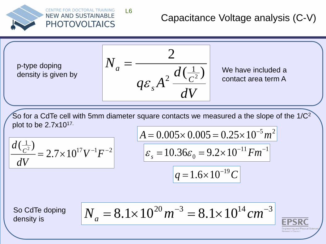
So for a CdTe cell with 5mm diameter square contacts we measured a the slope of the 1/C2 plot to be 2.7x10¹⁷.
dVd
AqN
Cs
a )(2
21
2ε=
21171
107.2)( 2 −−×= FV
dVd
C
251025.0005.0005.0 mA −×=×=111
0 102.936.10 −−×== Fms εε
Cq 19106.1 −×=
314320 101.8101.8 −− ×=×= cmmNaSo CdTe doping density is
p-type doping density is given by We have included a
contact area term A

Summary LX
• JV – RS and RSH can infer the issue
• J-V-T – Back contact barrier height measurements
• EQE – Layer behaviour and optical losses
• CV - doping density of p-type layer
Key junction characterisation techniques