lead selenide nanowire growth by vapor-liquid-solid mechanism under mask during plasma processing
TRANSCRIPT
ISSN 1063�7850, Technical Physics Letters, 2011, Vol. 37, No. 10, pp. 929–931. © Pleiades Publishing, Ltd., 2011.Original Russian Text © S.P. Zimin, E.S. Gorlachev, I.I. Amirov, V.V. Naumov, 2011, published in Pis’ma v Zhurnal Tekhnicheskoi Fiziki, 2011, Vol. 37, No. 19, pp. 80–87.
929
In recent years, there has been an increasing num�ber of publications devoted to one�dimensional nano�structures (nanowires, NWs) that are of interest fromthe standpoint of both basic research and practicalapplications [1, 2]. As a rule, NWs are obtained by themethods of so�called “bottom�up” deposition andepitaxial growth. The most universal mechanism ofone�dimensional nanostructure formation is their cat�alytic growth according to the vapor–liquid–solid(VLS) mechanism [3]. Both the physical theory andpractical aspects of this mechanism have been wellstudied [4–6]. Of special interest is the fabrication ofNWs based on lead chalcogenides PbX (X = Te, Se, S),for which the VLS mechanism provides both growth ofone�dimensional nanostructures with high degrees ofcrystallinity [7, 8] and formation of complicated net�works and hierarchical systems [9–11]. Owing to someunique properties of lead chalcogenides [12], theobtained nanostructures offer promising materials fornew�generation IR optoelectronic [13] and micro�thermoelectric [14] devices. However, the integrationof PbX nanowires into Si�based electronic devicesrequires developing an efficient and universal methodfor the NW growth on preset surface areas within theframework of traditional “top�down” operations, inparticular, plasma processing.
This Letter presents the results of an investigationof the formation of one�dimensional nanostructuresof lead chalcogenide on the surface of PbSe film undera mask at the stage of selective plasma etching.
The initial samples were PbSe films with thick�nesses within 1.5–5 µm grown by molecular beam epi�taxy (ETH, Zurich) on Si(111) single crystal substrateswith 2� to 4�nm�thick CaF2 buffer layers [13]. Theobtained PbSe/CaF2/Si(111) epitaxial structures wereprocessed in high�density inductively coupled plasma
(ICP) of low�pressure argon RF discharge [15, 16] atan RF bias power of 200–400 W supplied to the sub�strate holder electrode. The RF�ICP etching processwas performed using a stencil mask represented by380�µm�thick single�crystalline silicon wafer with aperiodic array of circular holes with a diameter of75 µm. The mask was spaced by several microns fromthe PbSe film surface. Since the rate of silicon sputter�ing in RF�ICP under the conditions employed wassignificantly lower than the sputtering rate of binaryPbX compounds [16], the exposed regions of Si sub�strate remained almost unetched.
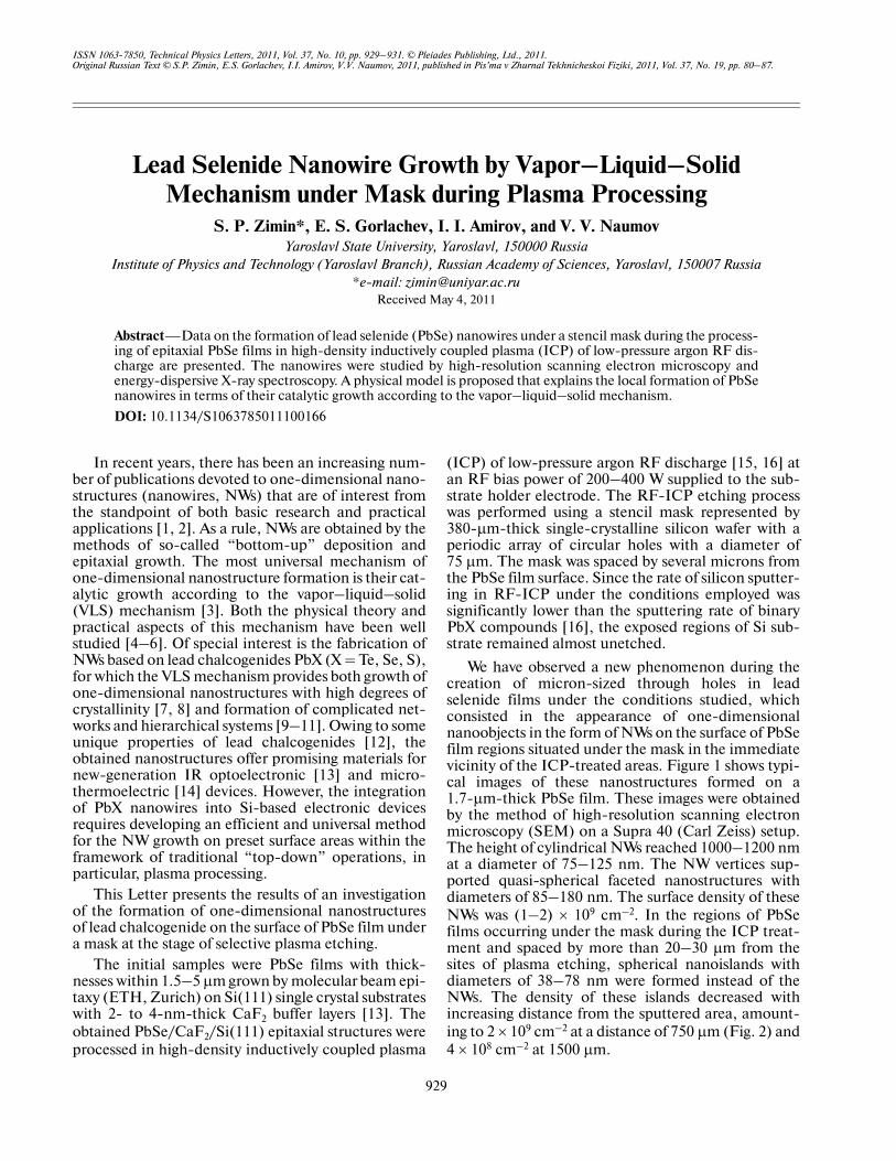
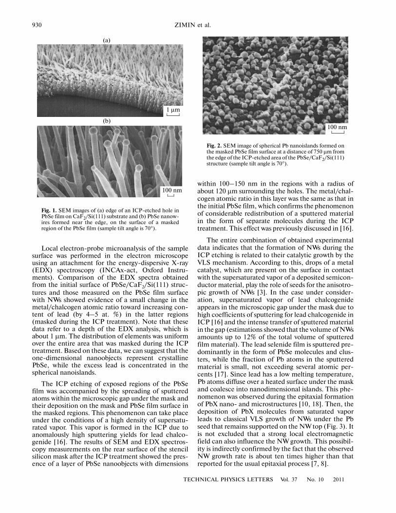
We have observed a new phenomenon during thecreation of micron�sized through holes in leadselenide films under the conditions studied, whichconsisted in the appearance of one�dimensionalnanoobjects in the form of NWs on the surface of PbSefilm regions situated under the mask in the immediatevicinity of the ICP�treated areas. Figure 1 shows typi�cal images of these nanostructures formed on a1.7�µm�thick PbSe film. These images were obtainedby the method of high�resolution scanning electronmicroscopy (SEM) on a Supra 40 (Carl Zeiss) setup.The height of cylindrical NWs reached 1000–1200 nmat a diameter of 75–125 nm. The NW vertices sup�ported quasi�spherical faceted nanostructures withdiameters of 85–180 nm. The surface density of theseNWs was (1–2) × 109 cm–2. In the regions of PbSefilms occurring under the mask during the ICP treat�ment and spaced by more than 20–30 µm from thesites of plasma etching, spherical nanoislands withdiameters of 38–78 nm were formed instead of theNWs. The density of these islands decreased withincreasing distance from the sputtered area, amount�ing to 2 × 109 cm–2 at a distance of 750 µm (Fig. 2) and4 × 108 cm–2 at 1500 µm.
Lead Selenide Nanowire Growth by Vapor–Liquid–Solid Mechanism under Mask during Plasma Processing
S. P. Zimin*, E. S. Gorlachev, I. I. Amirov, and V. V. NaumovYaroslavl State University, Yaroslavl, 150000 Russia
Institute of Physics and Technology (Yaroslavl Branch), Russian Academy of Sciences, Yaroslavl, 150007 Russia*e�mail: [email protected]
Received May 4, 2011
Abstract—Data on the formation of lead selenide (PbSe) nanowires under a stencil mask during the process�ing of epitaxial PbSe films in high�density inductively coupled plasma (ICP) of low�pressure argon RF dis�charge are presented. The nanowires were studied by high�resolution scanning electron microscopy andenergy�dispersive X�ray spectroscopy. A physical model is proposed that explains the local formation of PbSenanowires in terms of their catalytic growth according to the vapor–liquid–solid mechanism.
DOI: 10.1134/S1063785011100166
930
TECHNICAL PHYSICS LETTERS Vol. 37 No. 10 2011
ZIMIN et al.
Local electron�probe microanalysis of the samplesurface was performed in the electron microscopeusing an attachment for the energy�dispersive X�ray(EDX) spectroscopy (INCAx�act, Oxford Instru�ments). Comparison of the EDX spectra obtainedfrom the initial surface of PbSe/CaF2/Si(111) struc�tures and those measured on the PbSe film surfacewith NWs showed evidence of a small change in themetal/chalcogen atomic ratio toward increasing con�tent of lead (by 4–5 at. %) in the latter regions(masked during the ICP treatment). Note that thesedata refer to a depth of the EDX analysis, which isabout 1 µm. The distribution of elements was uniformover the entire area that was masked during the ICPtreatment. Based on these data, we can suggest that theone�dimensional nanoobjects represent crystallinePbSe, while the excess lead is concentrated in thespherical nanoislands.
The ICP etching of exposed regions of the PbSefilm was accompanied by the spreading of sputteredatoms within the microscopic gap under the mask andtheir deposition on the mask and PbSe film surface inthe masked regions. This phenomenon can take placeunder the conditions of a high density of supersatu�rated vapor. This vapor is formed in the ICP due toanomalously high sputtering yields for lead chalco�genide [16]. The results of SEM and EDX spectros�copy measurements on the rear surface of the stencilsilicon mask after the ICP treatment showed the pres�ence of a layer of PbSe nanoobjects with dimensions
within 100–150 nm in the regions with a radius ofabout 120 µm surrounding the holes. The metal/chal�cogen atomic ratio in this layer was the same as that inthe initial PbSe film, which confirms the phenomenonof considerable redistribution of a sputtered materialin the form of separate molecules during the ICPtreatment. This effect was previously discussed in [16].
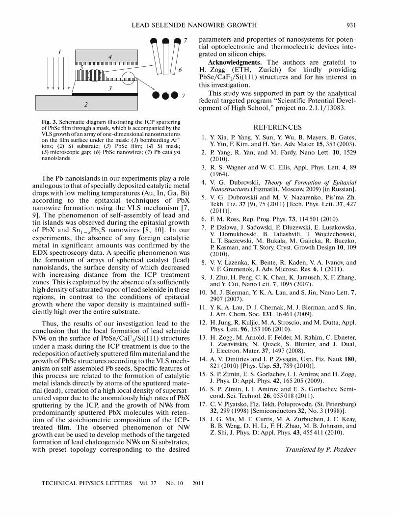
The entire combination of obtained experimentaldata indicates that the formation of NWs during theICP etching is related to their catalytic growth by theVLS mechanism. According to this, drops of a metalcatalyst, which are present on the surface in contactwith the supersaturated vapor of a deposited semicon�ductor material, play the role of seeds for the anisotro�pic growth of NWs [3]. In the case under consider�ation, supersaturated vapor of lead chalcogenideappears in the microscopic gap under the mask due tohigh coefficients of sputtering for lead chalcogenide inICP [16] and the intense transfer of sputtered materialin the gap (estimations showed that the volume of NWsamounts up to 12% of the total volume of sputteredfilm material). The lead selenide film is sputtered pre�dominantly in the form of PbSe molecules and clus�ters, while the fraction of Pb atoms in the sputteredmaterial is small, not exceeding several atomic per�cents [17]. Since lead has a low melting temperature,Pb atoms diffuse over a heated surface under the maskand coalesce into nanodimensional islands. This phe�nomenon was observed during the epitaxial formationof PbX nano� and microstructures [10, 18]. Then, thedeposition of PbX molecules from saturated vaporleads to classical VLS growth of NWs under the Pbseed that remains supported on the NW top (Fig. 3). Itis not excluded that a strong local electromagneticfield can also influence the NW growth. This possibil�ity is indirectly confirmed by the fact that the observedNW growth rate is about ten times higher than thatreported for the usual epitaxial process [7, 8].
1 µm
100 nm
Fig. 1. SEM images of (a) edge of an ICP�etched hole inPbSe film on CaF2/Si(111) substrate and (b) PbSe nanow�ires formed near the edge, on the surface of a maskedregion of the PbSe film (sample tilt angle is 70°).
100 nm
Fig. 2. SEM image of spherical Pb nanoislands formed onthe masked PbSe film surface at a distance of 750 µm fromthe edge of the ICP�etched area of the PbSe/CaF2/Si(111)structure (sample tilt angle is 70°).
(a)
(b)
TECHNICAL PHYSICS LETTERS Vol. 37 No. 10 2011
LEAD SELENIDE NANOWIRE GROWTH 931
The Pb nanoislands in our experiments play a roleanalogous to that of specially deposited catalytic metaldrops with low melting temperatures (Au, In, Ga, Bi)according to the epitaxial techniques of PbXnanowire formation using the VLS mechanism [7,9]. The phenomenon of self�assembly of lead andtin islands was observed during the epitaxial growthof PbX and Sn1 – xPbxS nanowires [8, 10]. In ourexperiments, the absence of any foreign catalyticmetal in significant amounts was confirmed by theEDX spectroscopy data. A specific phenomenon wasthe formation of arrays of spherical catalyst (lead)nanoislands, the surface density of which decreasedwith increasing distance from the ICP treatmentzones. This is explained by the absence of a sufficientlyhigh density of saturated vapor of lead selenide in theseregions, in contrast to the conditions of epitaxialgrowth where the vapor density is maintained suffi�ciently high over the entire substrate.
Thus, the results of our investigation lead to theconclusion that the local formation of lead selenideNWs on the surface of PbSe/CaF2/Si(111) structuresunder a mask during the ICP treatment is due to theredeposition of actively sputtered film material and thegrowth of PbSe structures according to the VLS mech�anism on self�assembled Pb seeds. Specific features ofthis process are related to the formation of catalyticmetal islands directly by atoms of the sputtered mate�rial (lead), creation of a high local density of supersat�urated vapor due to the anomalously high rates of PbXsputtering by the ICP, and the growth of NWs frompredominantly sputtered PbX molecules with reten�tion of the stoichiometric composition of the ICP�treated film. The observed phenomenon of NWgrowth can be used to develop methods of the targetedformation of lead chalcogenide NWs on Si substrates,with preset topology corresponding to the desired
parameters and properties of nanosystems for poten�tial optoelectronic and thermoelectric devices inte�grated on silicon chips.
Acknowledgments. The authors are grateful toH. Zogg (ETH, Zurich) for kindly providingPbSe/CaF2/Si(111) structures and for his interest inthis investigation.
This study was supported in part by the analyticalfederal targeted program “Scientific Potential Devel�opment of High School,” project no. 2.1.1/13083.
REFERENCES
1. Y. Xia, P. Yang, Y. Sun, Y. Wu, B. Mayers, B. Gates,Y. Yin, F. Kim, and H. Yan, Adv. Mater. 15, 353 (2003).
2. P. Yang, R. Yan, and M. Fardy, Nano Lett. 10, 1529(2010).
3. R. S. Wagner and W. C. Ellis, Appl. Phys. Lett. 4, 89(1964).
4. V. G. Dubrovskii, Theory of Formation of EpitaxialNanostructures (Fizmatlit, Moscow, 2009) [in Russian].
5. V. G. Dubrovskii and M. V. Nazarenko, Pis’ma Zh.Tekh. Fiz. 37 (9), 75 (2011) [Tech. Phys. Lett. 37, 427(2011)].
6. F. M. Ross, Rep. Prog. Phys. 73, 114 501 (2010).7. P. Dziawa, J. Sadowski, P. Dluzewski, E. Lusakowska,
V. Domukhovski, B. Taliashvili, T. Wojciechowski,L. T. Baczewski, M. Bukala, M. Galicka, R. Buczko,P. Kasman, and T. Story, Cryst. Growth Design 10, 109(2010).
8. V. V. Lazenka, K. Bente, R. Kaden, V. A. Ivanov, andV. F. Gremenok, J. Adv. Microsc. Res. 6, 1 (2011).
9. J. Zhu, H. Peng, C. K. Chan, K. Jarausch, X. F. Zhang,and Y. Cui, Nano Lett. 7, 1095 (2007).
10. M. J. Bierman, Y. K. A. Lau, and S. Jin, Nano Lett. 7,2907 (2007).
11. Y. K. A. Lau, D. J. Chernak, M. J. Bierman, and S. Jin,J. Am. Chem. Soc. 131, 16 461 (2009).
12. H. Jung, R. Kuljic, M. A. Stroscio, and M. Dutta, Appl.Phys. Lett. 96, 153 106 (2010).
13. H. Zogg, M. Arnold, F. Felder, M. Rahim, C. Ebneter,I. Zasavitskiy, N. Quack, S. Blunier, and J. Dual,J. Electron. Mater. 37, 1497 (2008).
14. A. V. Dmitriev and I. P. Zvyagin, Usp. Fiz. Nauk 180,821 (2010) [Phys. Usp. 53, 789 (2010)].
15. S. P. Zimin, E. S. Gorlachev, I. I. Amirov, and H. Zogg,J. Phys. D: Appl. Phys. 42, 165 205 (2009).
16. S. P. Zimin, I. I. Amirov, and E. S. Gorlachev, Semi�cond. Sci. Technol. 26, 055 018 (2011).
17. C. V. Plyatsko, Fiz. Tekh. Poluprovodn. (St. Petersburg)32, 299 (1998) [Semiconductors 32, No. 3 (1998)].
18. J. G. Ma, M. E. Curtis, M. A. Zurbuchen, J. C. Keay,B. B. Weng, D. H. Li, F. H. Zhao, M. B. Johnson, andZ. Shi, J. Phys. D: Appl. Phys. 43, 455 411 (2010).
Translated by P. Pozdeev
14
5
3
2
7
6
7
Fig. 3. Schematic diagram illustrating the ICP sputteringof PbSe film through a mask, which is accompanied by theVLS growth of an array of one�dimensional nanostructureson the film surface under the mask: (1) bombarding Ar+
ions; (2) Si substrate; (3) PbSe film; (4) Si mask;(5) microscopic gap; (6) PbSe nanowires; (7) Pb catalystnanoislands.