lcc & llc resonant converter for high-power, low … 785 lcc & llc resonant converter for...
TRANSCRIPT
Page 785
LCC & LLC Resonant Converter For High-Power, Low-Voltage,
High-Current Power Applications B.Anurag
M.Tech (Power Electronics),
Dept of EEE,
St.Martin’s Engineering College.
V.Sunil Kumar, M.E (EPS)
Associate Professor,
Dept of EEE,
St.Martin’s Engineering College.
ABSTRACT:
LCC thunderous converter with inductive channel
working in spasmodic current mode (DCM) can
accomplish zero-current exchanging (ZCS) for both
the force switches and rectifier diodes. In this way, it is
appropriate for high-control, low-voltage, high-current
force supplies. The DCM LCC resounding converter
with inductive channel may work in various working
modes when info voltage or burden changes, which
challenges the outline. This paper infers a mode limit
map, from which the working method of the converter
can be effectively decided. In light of the mode limit
outline, summed up ideal configuration technique is
proposed and an arrangement of ideal and standardized
converter parameters is resolved, which can be
effectively changed over into genuine parameters as
indicated by the converter detail. Three 5 kW models
with various converter parameters are created and tried
in the lab, and the exploratory results demonstrate that
with the arrangement of ideal parameters, the
converter can accomplish the most astounding
proficiency over the whole info voltage and burden
range.
Index Terms:
Discontinuous current mode (DCM), LCC resonant
converter, mode boundary map, optimal design, zero-
current switching (ZCS).
I. INTRODUCTION:
High-control, low-voltage, high-current force supplies
are broadly utilized as a part of electroplating [1],
electrolyzing [2], welding [3] and excitation for
superconducting magnet [4], and so on.
In these force supplies, IGBTs are usually utilized as
the force switches. It is liked to accomplish zero-
current exchanging (ZCS) for IGBTs to diminish the
turn-off misfortunes came about by the present tail [5].
Full converters are great possibility for accomplishing
ZCS. Arrangement full converter (SRC) [6] and
parallel thunderous converter (PRC) [7] are two
essential resounding converters. SRC offers high
productivity at light load, yet it has an extensive
variety of exchanging recurrence and its yield voltage
can't be controlled at a heap [8]. PRC has a restricted
scope of exchanging recurrence, and its yield voltage
can be controlled at no heap; be that as it may, the
effectiveness at light load is generally low [8].
Keeping in mind the end goal to beat the weaknesses
of SRC and PRC, different other full converters with
more than two thunderous parts have been proposed
[9], [10].
Among them, LLC full converter [11], [12] and LCC
thunderous converter [13]–[24] are the most well
known converters. The yield channel of a thunderous
converter can be either a capacitive channel or an
inductive channel [9], [10]. For the LLC full converter,
the yield channel ought to be the capacitive one. For
the LCC resounding converter, both the capacitive
channel [13]–[19] and inductive channel [20]–[24] can
be embraced. In high-control, low-voltage, high-
current force supplies, the inductive channel is alluring
since the present swell in the yield channel capacitor is
moderately littler contrasted with that in the capacitive
channel. There-fore, LCC thunderous converter with
inductive channel is appealing for these applications.
The LCC thunderous converter with inductive channel
can work in constant current mode (CCM) [20]–[22]
Page 786
or intermittent current mode (DCM) [23], [24]. In
CCM, if the LCC resounding converter with inductive
channel works above reverberation, the force switches
can accomplish zero-voltage exchanging (ZVS) [20],
[21]; on the off chance that it works beneath
reverberation, the force switches can accomplish ZCS
turn-off, however hard turn-on [22]. In DCM, both the
ZCS turn-on and turn-off can be accomplished,
prompting low exchanging misfortunes [23], [24]. In
this way, letting the LCC thunderous converter with
inductive channel to work in DCM is a superior
decision for high-control, low-voltage, high-current
applications.
The framework of LCC reverberating converter has
been extensively inspected [13]–[24], and the DCM
LCC full converter with inductive channel has been
based on in [23] and [24]. The DCM LCC deafening
converter with inductive direct can work in various
working modes, and the working mode may change
with the assortments of information voltage and
weight, which challenges the layout of the converter
parameters. In [23] and [24], two distinctive working
modes are considered for configuration, separately,
and in this way, the converter has not been enhanced
with varieties of the info voltage and burden. Besides,
outlines depend on the particular determinations of the
converters.
For different details, the converter ought to be
overhauled. To tackle these issues, this paper proposes
the idea of the mode limit map for the DCM LCC full
converter with inductive channel, from which the
working method of the converter can be effortlessly
decided. In light of the mode limit delineate, summed
up ideal outline system with the varieties of
information voltage and burden is proposed and an
arrangement of standardized converter parameters is
resolved, which can be effectively changed over into
genuine converter parameters, regardless of what the
converter particular is. With this arrangement of
parameters, the converter can accomplish a high
effectiveness over the whole information voltage and
burden ranges.
This paper is sorted out as takes after. In Section II,
the conceivable working methods of the DCM LCC
resounding converter with inductive channel are
quickly looked into. In Section III, the mode limit
guide is determined. In Section IV, the enduring state
qualities of the converter are given. In Section V, an
arrangement of ideal and standardized converter
parameters is resolved in view of the mode limit map.
In Section VI, three 50 V/100 A proto-sorts are
manufactured and tried. One model is planned with
the proposed set of ideal parameters; the other two
proto-sorts are utilized for examinations. In these two
models, one is outlined with the arrangement of
parameters from [24], and the other is composed with
the parameters so it goes about as a DCM PRC. The
test comes about check that the model with the
proposed set of parameters accomplishes a higher
effectiveness than the other two models over the
whole information voltage and burden range. At long
last, Section VII finishes up this paper.
II. REVIEW OF OPERATING MODES OF DCM
LCC RESONANT CONVERTER WITH
INDUCTIVE FILTER
Fig. 1 demonstrates the primary circuit of the LCC
resounding converter with inductive channel. The
parallel full capacitor Cp is purposefully set on the
auxiliary side of the transformer to make utilization of
the spillage inductor of the transformer as a part of the
thunderous inductor. The inductor Lr speaks to the
aggregate of the resounding inductor and the spillage
inductor of the transformer. Lf and Cf form the
inductive channel. The converter is operated in DCM
by gating the switches Q1−Q4 with an altered on-time
and variable recurrence to manage the yield voltage.
Before investigation, it is accepted that every one of
the segments are perfect and Lf is sufficiently vast to
be viewed as a present source with the estimation of
yield current Io. Because of the symmetrical operation,
just the half cycle when Q1 and Q4 are leading is
investigated here. Fig. 2 demonstrates all the
conceivable identical circuits during diverse working
interims down the middle cycle, where the circuit
shaped by Lf , Cf , and RL d is improved to the present
Page 787
source Io and the parallel thunderous capacitor Cp is
reflected to the essential side of the transformer, meant
by Cp.
Fig.1.Main circuit of the LCC resonant converter
with inductive filter.
Interval 0 [Prior to 0]:
iLr=0 and the load currentIofreewheels through DR1 and
DR2 . Therefore, vCp = 0 and vC s has an initial value.
Interval 1 [t0, t1 ]: Att0,Q1, andQ4are turned on with
ZCS,andVin is applied on the resonant tank.
Consequently, Lr and Csstart to resonate,
andiLrincreases from zero. AsiLr<Io/n, DR1and DR2still
keep conducting andvCp=0.
Interval 2 [After t1]:
Att1,iLrincreasestoIo/n.DR2turnsoff naturally, and Io
flows through DR1 . After t1,iLr>Io /n. Hence, Cp is
charged and vCp increases from zero. Lr ,Cs , and
Cpstart to resonate.Over the span of reverberation, iLr
will cross zero twice: the first run through is that iLr
crosses zero from the positive bearing, indicated by
ti+; and the second time is that iLr crosses zero from
the negative course, meant by ti−. vC p will cross zero
once from the positive course, meant by tv+. tv+ could
be later than ti−, inside [ti+ , ti−], or sooner than ti+ ,
and this will prompt three conceivable working modes,
which are named as Mode 1, Mode 2, and Mode 3,
separately. The key working waveforms of these three
working modes are appeared in Fig. 3. In these
working modes, Q1 and Q4 are killed with ZCS when
iLr decreases to negative and moves through D1 and
D4 during [ti+,ti−].At the point when both iLr and v
Cp return to zero, the converter will come back to
Interval 0. The nitty gritty conditions of Mode 1 and
Mode 2 can be found from [23] and [24], separately.
The standardized types of the conditions of all these
three working modes are determined in Appendix A.
The physical amounts in these conditions are
standardized as for the base amounts characterized in
Table I. Unfaltering state arrangements of the
converter can be gotten from these conditions.
Fig. 2. Possible operating intervals in half cycle.(a)
Interval 0. (b) Interval 1.(c) Interval 2. (d) Interval
3
TABLE I: DEFINITION OF BASE QUANTITIES
Page 788
Fig. 3. Key operating waveforms. (a) Mode 1. (b)
Mode 2. (c) Mode 3.
III. DERIVATION OF THE MODE
BOUNDARY MAP
A. Boundary Curve between Mode 1 and Non-ZCS
Area:
As seen in Fig. 3(a), LrCs and Cp resonate after t1 in
Mode 1. In order to achieve ZCS turn-off for the
power switches, iLr should cross zero. So, according to
(A8), we have
According to (1), the boundary condition between
Mode 1 and non-ZCS area is
Combining and solving (2), (A5), (A9), (A11), and
(A16) can obtain the equation of the boundary curve of
Mode 1 and non-ZCS area as
whereIo N = IoZr/(nVin ), λ = Cp/Cs . The detailed
derivation of (3) is shown in Appendix B. According
to (3), Curve 1, which is the boundary curve between
Mode 1 and non-ZCS area, is drawn in Fig. 4.
B. Boundary Curve Between Mode 1 and Mode 2
tv+=ti−is the boundary condition between Mode 1
andMode 2. This implies VC pN 2 = 0 in Mode 1.
Likewise, combining and solving VC pN 2 = 0, (A5),
(A9)–(A11), and (A16), the boundary curve equation
between Mode 1 and Mode 2 can be derived as
Fig. 4.Mode boundary map of DCM LCC resonant
converter with inductive filter.
According to (4), Curve 2, which is the boundary
curve be-tween Mode 1 and Mode 2, is drawn in Fig.
4.
C. Boundary Curve Between Mode 2 and Mode 3
tv+=ti+is the boundary condition between Mode 2
andMode 3. This implies IL rN 2 = 0 in Mode 2.
Likewise, solving IL rN 2=0, (A5), (A17)–(A19), (A23),
(A24), and (A25), theequation of the boundary curve
between Mode 2 and Mode 3 can be derived as
Page 789
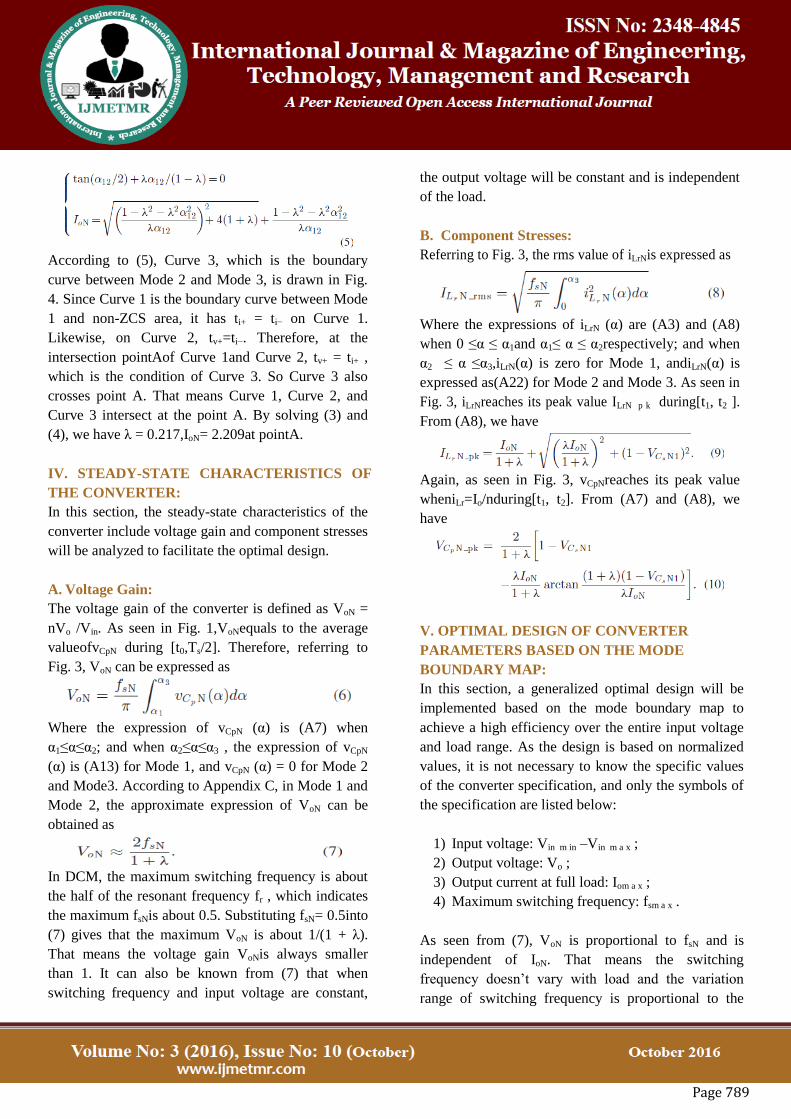
According to (5), Curve 3, which is the boundary
curve between Mode 2 and Mode 3, is drawn in Fig.
4. Since Curve 1 is the boundary curve between Mode
1 and non-ZCS area, it has ti+ = ti− on Curve 1.
Likewise, on Curve 2, tv+=ti−. Therefore, at the
intersection pointAof Curve 1and Curve 2, tv+ = ti+ ,
which is the condition of Curve 3. So Curve 3 also
crosses point A. That means Curve 1, Curve 2, and
Curve 3 intersect at the point A. By solving (3) and
(4), we have λ = 0.217,IoN= 2.209at pointA.
IV. STEADY-STATE CHARACTERISTICS OF
THE CONVERTER:
In this section, the steady-state characteristics of the
converter include voltage gain and component stresses
will be analyzed to facilitate the optimal design.
A. Voltage Gain:
The voltage gain of the converter is defined as VoN =
nVo /Vin. As seen in Fig. 1,VoNequals to the average
valueofvCpN during [t0,Ts/2]. Therefore, referring to
Fig. 3, VoN can be expressed as
Where the expression of vCpN (α) is (A7) when
α1≤α≤α2; and when α2≤α≤α3 , the expression of vCpN
(α) is (A13) for Mode 1, and vCpN (α) = 0 for Mode 2
and Mode3. According to Appendix C, in Mode 1 and
Mode 2, the approximate expression of VoN can be
obtained as
In DCM, the maximum switching frequency is about
the half of the resonant frequency fr , which indicates
the maximum fsNis about 0.5. Substituting fsN= 0.5into
(7) gives that the maximum VoN is about 1/(1 + λ).
That means the voltage gain VoNis always smaller
than 1. It can also be known from (7) that when
switching frequency and input voltage are constant,
the output voltage will be constant and is independent
of the load.
B. Component Stresses:
Referring to Fig. 3, the rms value of iLrNis expressed as
Where the expressions of iLrN (α) are (A3) and (A8)
when 0 ≤α ≤ α1and α1≤ α ≤ α2respectively; and when
α2 ≤ α ≤α3,iLrN(α) is zero for Mode 1, andiLrN(α) is
expressed as(A22) for Mode 2 and Mode 3. As seen in
Fig. 3, iLrNreaches its peak value ILrN p k during[t1, t2 ].
From (A8), we have
Again, as seen in Fig. 3, vCpNreaches its peak value
wheniLr=Io/nduring[t1, t2]. From (A7) and (A8), we
have
V. OPTIMAL DESIGN OF CONVERTER
PARAMETERS BASED ON THE MODE
BOUNDARY MAP:
In this section, a generalized optimal design will be
implemented based on the mode boundary map to
achieve a high efficiency over the entire input voltage
and load range. As the design is based on normalized
values, it is not necessary to know the specific values
of the converter specification, and only the symbols of
the specification are listed below:
1) Input voltage: Vin m in –Vin m a x ;
2) Output voltage: Vo ;
3) Output current at full load: Iom a x ;
4) Maximum switching frequency: fsm a x .
As seen from (7), VoN is proportional to fsN and is
independent of IoN. That means the switching
frequency doesn’t vary with load and the variation
range of switching frequency is proportional to the
Page 790
variation range of input voltage. Therefore, the range
of switching frequency cannot be reduced and when
the maximum switching frequency fsmax is given, the
minimum switching frequency is determined by the
range of input voltage. In order to improve the converter
efficiency, we should reduce the switching losses and
conduction losses. Since the power switches can
realize ZCS, the switching losses are quite small and
can be ignored compared with conduction losses.
Therefore, in order to improve the converter efficiency,
we should mainly reduce the conduction losses, which
mean the circulating current of the resonant tank should
be reduced. Since the circulating current of the resonant
tank will be reduced with the reduction of the energy
that is fed back to the input voltage by the resonant tank.
So the optimization goal is to achieve the lowest
energy that is fed back to the input voltage by the
resonant tank.
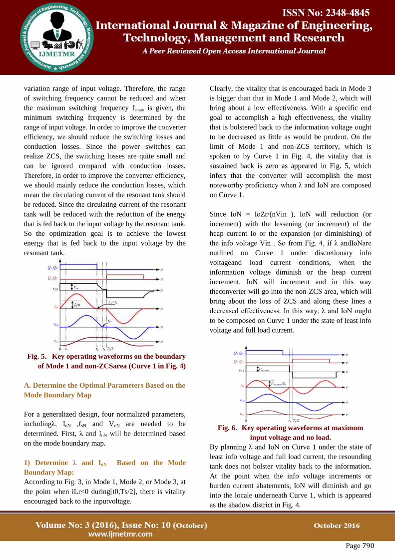
Fig. 5. Key operating waveforms on the boundary
of Mode 1 and non-ZCSarea (Curve 1 in Fig. 4)
A. Determine the Optimal Parameters Based on the
Mode Boundary Map
For a generalized design, four normalized parameters,
includingλ, IoN ,fsN and VoN are needed to be
determined. First, λ and IoN will be determined based
on the mode boundary map.
1) Determine λ and IoN Based on the Mode
Boundary Map:
According to Fig. 3, in Mode 1, Mode 2, or Mode 3, at
the point when iLr<0 during[t0,Ts/2], there is vitality
encouraged back to the inputvoltage.
Clearly, the vitality that is encouraged back in Mode 3
is bigger than that in Mode 1 and Mode 2, which will
bring about a low effectiveness. With a specific end
goal to accomplish a high effectiveness, the vitality
that is bolstered back to the information voltage ought
to be decreased as little as would be prudent. On the
limit of Mode 1 and non-ZCS territory, which is
spoken to by Curve 1 in Fig. 4, the vitality that is
sustained back is zero as appeared in Fig. 5, which
infers that the converter will accomplish the most
noteworthy proficiency when λ and IoN are composed
on Curve 1.
Since IoN = IoZr/(nVin ), IoN will reduction (or
increment) with the lessening (or increment) of the
heap current Io or the expansion (or diminishing) of
the info voltage Vin . So from Fig. 4, if λ andIoNare
outlined on Curve 1 under discretionary info
voltageand load current conditions, when the
information voltage diminish or the heap current
increment, IoN will increment and in this way
theconverter will go into the non-ZCS area, which will
bring about the loss of ZCS and along these lines a
decreased effectiveness. In this way, λ and IoN ought
to be composed on Curve 1 under the state of least info
voltage and full load current.
Fig. 6. Key operating waveforms at maximum
input voltage and no load.
By planning λ and IoN on Curve 1 under the state of
least info voltage and full load current, the resounding
tank does not bolster vitality back to the information.
At the point when the info voltage increments or
burden current abatements, IoN will diminish and go
into the locale underneath Curve 1, which is appeared
as the shadow district in Fig. 4.
Page 791
As of now, there is vitality bolstered back to the info.
The vitality encouraged back achieves its biggest
worth at most extreme info voltage and no heap, and
for this situation, the pinnacle current of iLr
equivalents to Vin m a x/Zr as appeared in Fig. 6.
Keeping in mind the end goal to decrease the vitality
nourished back at most extreme information voltage
and noload, the trademark impedance of the
thunderous tank, Zr , ought to be intended to be bigger.
From Fig. 4, it can be watched that on Curve 1, when λ
expands, IoN will increment. Since IoN=Iom a
xZr/(nVin m in),Zris around proportionaltoIoN . That
implies if λ is planned bigger, Zr can be intended to be
bigger. In any case, if λ is intended to be bigger than
the worth at point A, the converter will get into Mode
3 and the productivity will be debased. In this manner,
λ and IoN at least information voltage and full load
current are chosen at point An is the ideal decision.
2) Determine fsN and VoN :
As talked about above, λ and IoN at minimum
information voltage and full load current ought to be
planned at point A to minimize the vitality bolstered
back to the information voltage, and in this manner to
enhance the converter productivity. To encourage
enhance the converter productivity, the time interim
while iLr = 0 ought to be lessened, which relates to the
time interim from t3 to Ts/2, as appeared in Fig. 5,
since amid this time interim, the input voltage does not
give vitality to the resounding tank. So it is best to
diminish this time interim to zero, and hence, the
converter works in basic CCM at least information
voltage and full load current. At the point when the
information voltage increments or burden current
abatements, the converter will go into DCM. Along
these lines, fs Nat least info voltage and full load ought
to be designed as fsN = π/(α1 + α12 + α23), so that the
converter works incritical CCM. Whenever λ, IoN and
fsN are all decided, VoN can be controlled by (6).
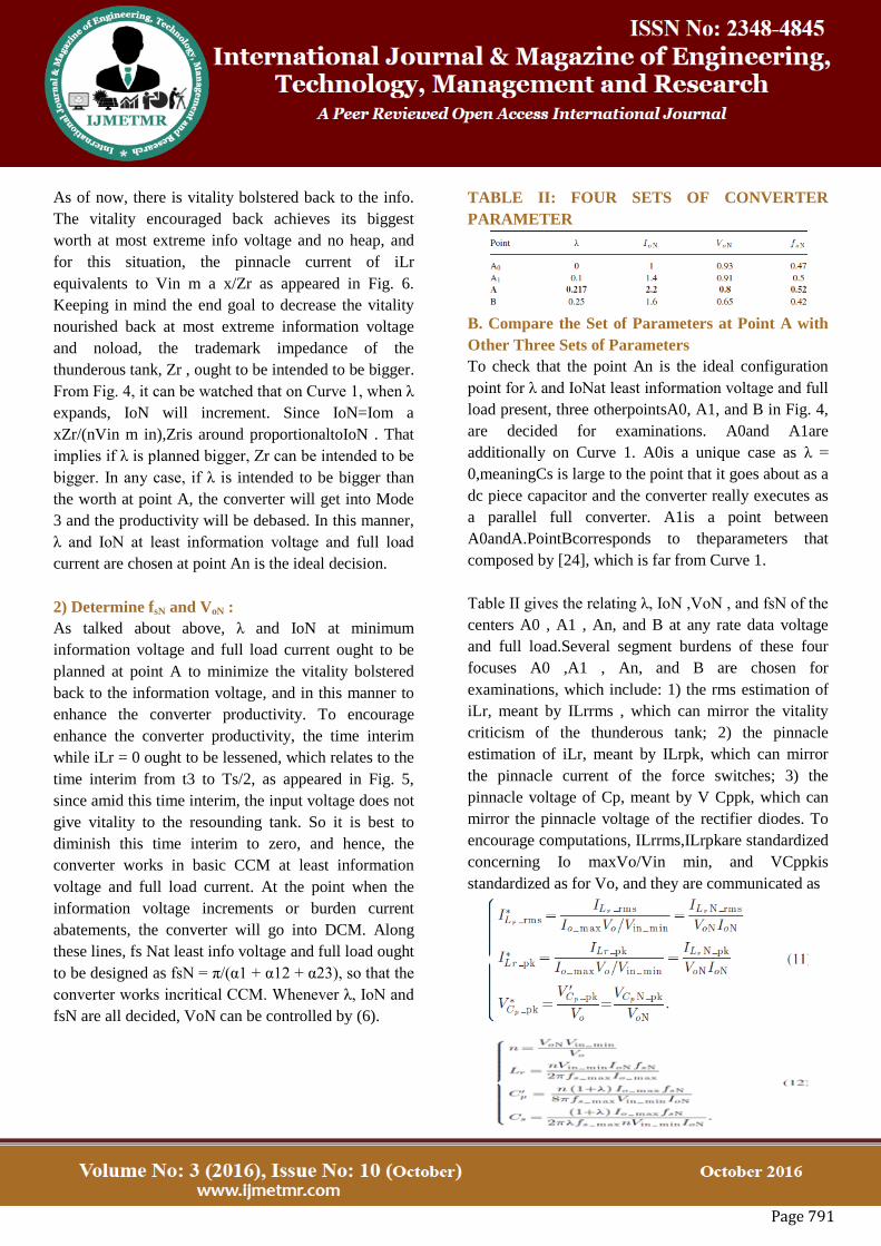
TABLE II: FOUR SETS OF CONVERTER
PARAMETER
B. Compare the Set of Parameters at Point A with
Other Three Sets of Parameters
To check that the point An is the ideal configuration
point for λ and IoNat least information voltage and full
load present, three otherpointsA0, A1, and B in Fig. 4,
are decided for examinations. A0and A1are
additionally on Curve 1. A0is a unique case as λ =
0,meaningCs is large to the point that it goes about as a
dc piece capacitor and the converter really executes as
a parallel full converter. A1is a point between
A0andA.PointBcorresponds to theparameters that
composed by [24], which is far from Curve 1.
Table II gives the relating λ, IoN ,VoN , and fsN of the
centers A0 , A1 , An, and B at any rate data voltage
and full load.Several segment burdens of these four
focuses A0 ,A1 , An, and B are chosen for
examinations, which include: 1) the rms estimation of
iLr, meant by ILrrms , which can mirror the vitality
criticism of the thunderous tank; 2) the pinnacle
estimation of iLr, meant by ILrpk, which can mirror
the pinnacle current of the force switches; 3) the
pinnacle voltage of Cp, meant by V Cppk, which can
mirror the pinnacle voltage of the rectifier diodes. To
encourage computations, ILrrms,ILrpkare standardized
concerning Io maxVo/Vin min, and VCppkis
standardized as for Vo, and they are communicated as
Page 792
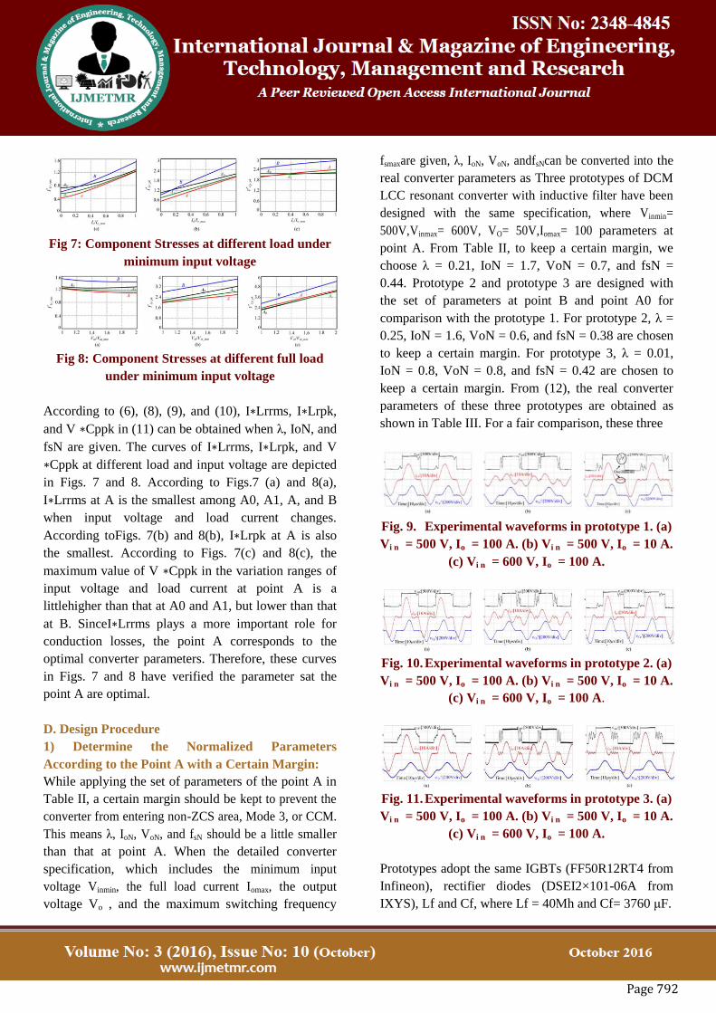
Fig 7: Component Stresses at different load under
minimum input voltage
Fig 8: Component Stresses at different full load
under minimum input voltage
According to (6), (8), (9), and (10), I∗Lrrms, I∗Lrpk,
and V ∗Cppk in (11) can be obtained when λ, IoN, and
fsN are given. The curves of I∗Lrrms, I∗Lrpk, and V
∗Cppk at different load and input voltage are depicted
in Figs. 7 and 8. According to Figs.7 (a) and 8(a),
I∗Lrrms at A is the smallest among A0, A1, A, and B
when input voltage and load current changes.
According toFigs. 7(b) and 8(b), I∗Lrpk at A is also
the smallest. According to Figs. 7(c) and 8(c), the
maximum value of V ∗Cppk in the variation ranges of
input voltage and load current at point A is a
littlehigher than that at A0 and A1, but lower than that
at B. SinceI∗Lrrms plays a more important role for
conduction losses, the point A corresponds to the
optimal converter parameters. Therefore, these curves
in Figs. 7 and 8 have verified the parameter sat the
point A are optimal.
D. Design Procedure
1) Determine the Normalized Parameters
According to the Point A with a Certain Margin:
While applying the set of parameters of the point A in
Table II, a certain margin should be kept to prevent the
converter from entering non-ZCS area, Mode 3, or CCM.
This means λ, IoN, VoN, and fsN should be a little smaller
than that at point A. When the detailed converter
specification, which includes the minimum input
voltage Vinmin, the full load current Iomax, the output
voltage Vo , and the maximum switching frequency
fsmaxare given, λ, IoN, VoN, andfsNcan be converted into the
real converter parameters as Three prototypes of DCM
LCC resonant converter with inductive filter have been
designed with the same specification, where Vinmin=
500V,Vinmax= 600V, VO= 50V,Iomax= 100 parameters at
point A. From Table II, to keep a certain margin, we
choose λ = 0.21, IoN = 1.7, VoN = 0.7, and fsN =
0.44. Prototype 2 and prototype 3 are designed with
the set of parameters at point B and point A0 for
comparison with the prototype 1. For prototype 2, λ =
0.25, IoN = 1.6, VoN = 0.6, and fsN = 0.38 are chosen
to keep a certain margin. For prototype 3, λ = 0.01,
IoN = 0.8, VoN = 0.8, and fsN = 0.42 are chosen to
keep a certain margin. From (12), the real converter
parameters of these three prototypes are obtained as
shown in Table III. For a fair comparison, these three
Fig. 9. Experimental waveforms in prototype 1. (a)
Vi n = 500 V, Io = 100 A. (b) Vi n = 500 V, Io = 10 A.
(c) Vi n = 600 V, Io = 100 A.
Fig. 10. Experimental waveforms in prototype 2. (a)
Vi n = 500 V, Io = 100 A. (b) Vi n = 500 V, Io = 10 A.
(c) Vi n = 600 V, Io = 100 A.
Fig. 11. Experimental waveforms in prototype 3. (a)
Vi n = 500 V, Io = 100 A. (b) Vi n = 500 V, Io = 10 A.
(c) Vi n = 600 V, Io = 100 A.
Prototypes adopt the same IGBTs (FF50R12RT4 from
Infineon), rectifier diodes (DSEI2×101-06A from
IXYS), Lf and Cf, where Lf = 40Μh and Cf= 3760 μF.
Page 793
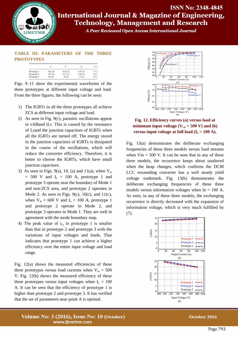
TABLE III: PARAMETERS OF THE THREE
PROTOTYPES
Figs. 9–11 show the experimental waveforms of the
three prototypes at different input voltage and load.
From the three figures, the following can be seen:
1) The IGBTs in all the three prototypes all achieve
ZCS at different input voltage and load.
2) As seen in Fig. 9(c), parasitic oscillations appear
in vABand iLr. This is caused by the resonance
of Lrand the junction capacitors of IGBTs when
all the IGBTs are turned off. The energy stored
in the junction capacitors of IGBTs is dissipated
in the course of the oscillations, which will
reduce the converter efficiency. Therefore, it is
better to choose the IGBTs, which have small
junction capacitors.
3) As seen in Figs. 9(a), 10, (a) and 11(a), when Vin
= 500 V and Io = 100 A, prototype 1 and
prototype 3 operate near the boundary of Mode 1
and non-ZCS area, and prototype 2 operates in
Mode 2. As seen in Figs. 9(c), 10(c), and 11(c),
when Vin = 600 V and Io = 100 A, prototype 1
and prototype 2 operate in Mode 2, and
prototype 3 operates in Mode 1. They are well in
agreement with the mode boundary map.
4) The peak value of iLr in prototype 1 is smaller
than that in prototype 2 and prototype 3 with the
variations of input voltages and loads. That
indicates that prototype 1 can achieve a higher
efficiency over the entire input voltage and load
range.
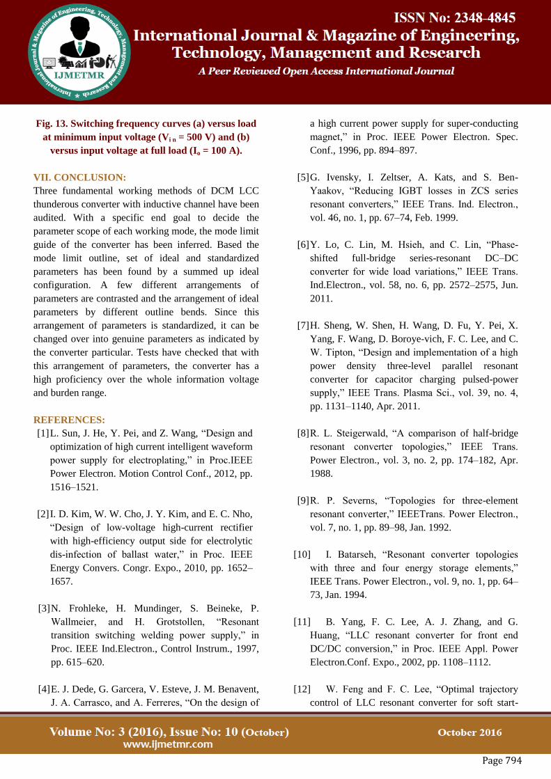
Fig. 12(a) shows the measured efficiencies of these
three prototypes versus load currents when Vin = 500
V. Fig. 12(b) shows the measured efficiency of these
three prototypes versus input voltages when Io = 100
A. It can be seen that the efficiency of prototype 1 is
higher than prototype 2 and prototype 3. It has verified
that the set of parameters near point A is optimal.
Fig. 12. Efficiency curves (a) versus load at
minimum input voltage (Vi n = 500 V) and (b)
versus input voltage at full load (Io = 100 A).
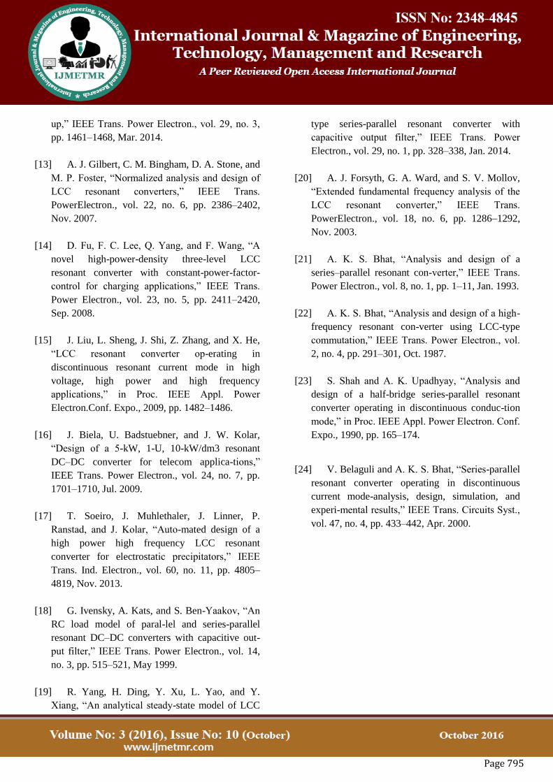
Fig. 13(a) demonstrates the deliberate exchanging
frequencies of these three models versus load streams
when Vin = 500 V. It can be seen that in any of these
three models, the recurrence keeps about unaltered
when the heap changes, which confirms the DCM
LCC resounding converter has a well steady yield
voltage trademark. Fig. 13(b) demonstrates the
deliberate exchanging frequencies of these three
models versus information voltages when Io = 100 A.
As seen, in any of these three models, the exchanging
recurrence is directly decreased with the expansion of
information voltage, which is very much fulfilled by
(7).
Page 794
Fig. 13. Switching frequency curves (a) versus load
at minimum input voltage (Vi n = 500 V) and (b)
versus input voltage at full load (Io = 100 A).
VII. CONCLUSION:
Three fundamental working methods of DCM LCC
thunderous converter with inductive channel have been
audited. With a specific end goal to decide the
parameter scope of each working mode, the mode limit
guide of the converter has been inferred. Based the
mode limit outline, set of ideal and standardized
parameters has been found by a summed up ideal
configuration. A few different arrangements of
parameters are contrasted and the arrangement of ideal
parameters by different outline bends. Since this
arrangement of parameters is standardized, it can be
changed over into genuine parameters as indicated by
the converter particular. Tests have checked that with
this arrangement of parameters, the converter has a
high proficiency over the whole information voltage
and burden range.
REFERENCES:
[1] L. Sun, J. He, Y. Pei, and Z. Wang, “Design and
optimization of high current intelligent waveform
power supply for electroplating,” in Proc.IEEE
Power Electron. Motion Control Conf., 2012, pp.
1516–1521.
[2] I. D. Kim, W. W. Cho, J. Y. Kim, and E. C. Nho,
“Design of low-voltage high-current rectifier
with high-efficiency output side for electrolytic
dis-infection of ballast water,” in Proc. IEEE
Energy Convers. Congr. Expo., 2010, pp. 1652–
1657.
[3] N. Frohleke, H. Mundinger, S. Beineke, P.
Wallmeier, and H. Grotstollen, “Resonant
transition switching welding power supply,” in
Proc. IEEE Ind.Electron., Control Instrum., 1997,
pp. 615–620.
[4] E. J. Dede, G. Garcera, V. Esteve, J. M. Benavent,
J. A. Carrasco, and A. Ferreres, “On the design of
a high current power supply for super-conducting
magnet,” in Proc. IEEE Power Electron. Spec.
Conf., 1996, pp. 894–897.
[5] G. Ivensky, I. Zeltser, A. Kats, and S. Ben-
Yaakov, “Reducing IGBT losses in ZCS series
resonant converters,” IEEE Trans. Ind. Electron.,
vol. 46, no. 1, pp. 67–74, Feb. 1999.
[6] Y. Lo, C. Lin, M. Hsieh, and C. Lin, “Phase-
shifted full-bridge series-resonant DC–DC
converter for wide load variations,” IEEE Trans.
Ind.Electron., vol. 58, no. 6, pp. 2572–2575, Jun.
2011.
[7] H. Sheng, W. Shen, H. Wang, D. Fu, Y. Pei, X.
Yang, F. Wang, D. Boroye-vich, F. C. Lee, and C.
W. Tipton, “Design and implementation of a high
power density three-level parallel resonant
converter for capacitor charging pulsed-power
supply,” IEEE Trans. Plasma Sci., vol. 39, no. 4,
pp. 1131–1140, Apr. 2011.
[8] R. L. Steigerwald, “A comparison of half-bridge
resonant converter topologies,” IEEE Trans.
Power Electron., vol. 3, no. 2, pp. 174–182, Apr.
1988.
[9] R. P. Severns, “Topologies for three-element
resonant converter,” IEEETrans. Power Electron.,
vol. 7, no. 1, pp. 89–98, Jan. 1992.
[10] I. Batarseh, “Resonant converter topologies
with three and four energy storage elements,”
IEEE Trans. Power Electron., vol. 9, no. 1, pp. 64–
73, Jan. 1994.
[11] B. Yang, F. C. Lee, A. J. Zhang, and G.
Huang, “LLC resonant converter for front end
DC/DC conversion,” in Proc. IEEE Appl. Power
Electron.Conf. Expo., 2002, pp. 1108–1112.
[12] W. Feng and F. C. Lee, “Optimal trajectory
control of LLC resonant converter for soft start-
Page 795
up,” IEEE Trans. Power Electron., vol. 29, no. 3,
pp. 1461–1468, Mar. 2014.
[13] A. J. Gilbert, C. M. Bingham, D. A. Stone, and
M. P. Foster, “Normalized analysis and design of
LCC resonant converters,” IEEE Trans.
PowerElectron., vol. 22, no. 6, pp. 2386–2402,
Nov. 2007.
[14] D. Fu, F. C. Lee, Q. Yang, and F. Wang, “A
novel high-power-density three-level LCC
resonant converter with constant-power-factor-
control for charging applications,” IEEE Trans.
Power Electron., vol. 23, no. 5, pp. 2411–2420,
Sep. 2008.
[15] J. Liu, L. Sheng, J. Shi, Z. Zhang, and X. He,
“LCC resonant converter op-erating in
discontinuous resonant current mode in high
voltage, high power and high frequency
applications,” in Proc. IEEE Appl. Power
Electron.Conf. Expo., 2009, pp. 1482–1486.
[16] J. Biela, U. Badstuebner, and J. W. Kolar,
“Design of a 5-kW, 1-U, 10-kW/dm3 resonant
DC–DC converter for telecom applica-tions,”
IEEE Trans. Power Electron., vol. 24, no. 7, pp.
1701–1710, Jul. 2009.
[17] T. Soeiro, J. Muhlethaler, J. Linner, P.
Ranstad, and J. Kolar, “Auto-mated design of a
high power high frequency LCC resonant
converter for electrostatic precipitators,” IEEE
Trans. Ind. Electron., vol. 60, no. 11, pp. 4805–
4819, Nov. 2013.
[18] G. Ivensky, A. Kats, and S. Ben-Yaakov, “An
RC load model of paral-lel and series-parallel
resonant DC–DC converters with capacitive out-
put filter,” IEEE Trans. Power Electron., vol. 14,
no. 3, pp. 515–521, May 1999.
[19] R. Yang, H. Ding, Y. Xu, L. Yao, and Y.
Xiang, “An analytical steady-state model of LCC
type series-parallel resonant converter with
capacitive output filter,” IEEE Trans. Power
Electron., vol. 29, no. 1, pp. 328–338, Jan. 2014.
[20] A. J. Forsyth, G. A. Ward, and S. V. Mollov,
“Extended fundamental frequency analysis of the
LCC resonant converter,” IEEE Trans.
PowerElectron., vol. 18, no. 6, pp. 1286–1292,
Nov. 2003.
[21] A. K. S. Bhat, “Analysis and design of a
series–parallel resonant con-verter,” IEEE Trans.
Power Electron., vol. 8, no. 1, pp. 1–11, Jan. 1993.
[22] A. K. S. Bhat, “Analysis and design of a high-
frequency resonant con-verter using LCC-type
commutation,” IEEE Trans. Power Electron., vol.
2, no. 4, pp. 291–301, Oct. 1987.
[23] S. Shah and A. K. Upadhyay, “Analysis and
design of a half-bridge series-parallel resonant
converter operating in discontinuous conduc-tion
mode,” in Proc. IEEE Appl. Power Electron. Conf.
Expo., 1990, pp. 165–174.
[24] V. Belaguli and A. K. S. Bhat, “Series-parallel
resonant converter operating in discontinuous
current mode-analysis, design, simulation, and
experi-mental results,” IEEE Trans. Circuits Syst.,
vol. 47, no. 4, pp. 433–442, Apr. 2000.