laboratory for interconnecting and packaging electronic ... · pdf filefaculty of microsystem...
TRANSCRIPT
Faculty of Microsystem Electronics
and Photonics
Laboratory for Interconnecting
and Packaging
Electronic Circuits
Wrocław, Poland
http://www.lipec.info
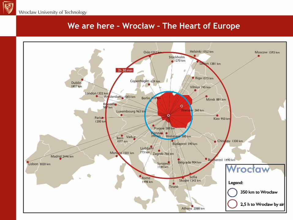
We are here – Wrocław – The Heart of Europe
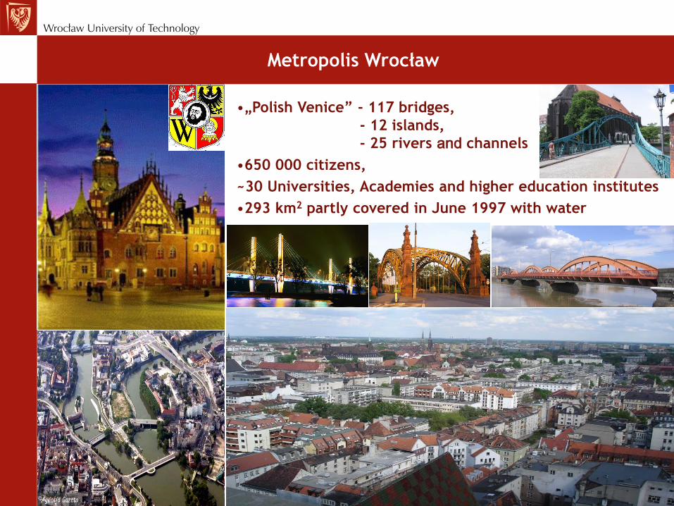
Metropolis Wrocław
•„Polish Venice” - 117 bridges,
- 12 islands,
- 25 rivers and channels
•650 000 citizens,
~30 Universities, Academies and higher education institutes
•293 km2 partly covered in June 1997 with water
Wrocław University of Technology
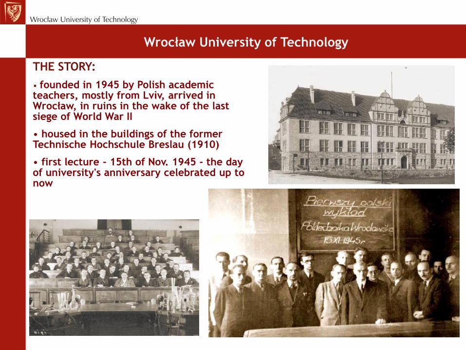
THE STORY:
• founded in 1945 by Polish academic teachers, mostly from Lviv, arrived in Wrocław, in ruins in the wake of the last siege of World War II
• housed in the buildings of the former Technische Hochschule Breslau (1910)
• first lecture - 15th of Nov. 1945 - the day of university's anniversary celebrated up to now
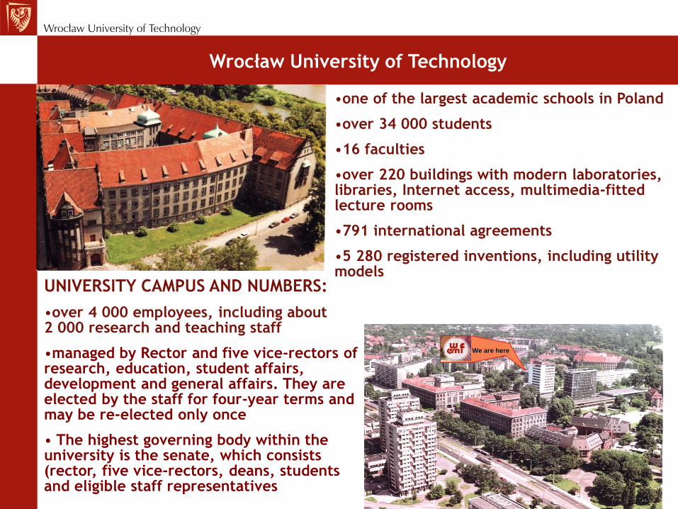
UNIVERSITY CAMPUS AND NUMBERS:
•over 4 000 employees, including about 2 000 research and teaching staff
•managed by Rector and five vice-rectors of research, education, student affairs, development and general affairs. They are elected by the staff for four-year terms and may be re-elected only once
• The highest governing body within the university is the senate, which consists (rector, five vice-rectors, deans, students and eligible staff representatives
Wrocław University of Technology
We are here
•one of the largest academic schools in Poland
•over 34 000 students
•16 faculties
•over 220 buildings with modern laboratories, libraries, Internet access, multimedia-fitted lecture rooms
•791 international agreements
•5 280 registered inventions, including utility models
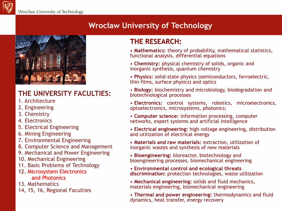
THE UNIVERSITY FACULTIES:1. Architecture
2. Engineering
3. Chemistry
4. Electronics
5. Electrical Engineering
6. Mining Engineering
7. Environmental Engineering 8. Computer Science and Management9. Mechanical and Power Engineering10. Mechanical Engineering11. Basic Problems of Technology12. Microsystem Electronics
and Photonics13. Mathematics14, 15, 16, Regional Faculties
THE RESEARCH:
• Mathematics: theory of probability, mathematical statistics, functional analysis, differential equations
• Chemistry: physical chemistry of solids, organic and inorganic synthesis, quantum chemistry
• Physics: solid-state physics (semiconductors, ferroelectric, thin films, surface physics) and optics
• Biology: biochemistry and microbiology, biodegradation and biotechnological processes
• Electronics: control systems, robotics, microelectronics,optoelectronics, microsystems, photonics;
• Computer science: information processing, computer networks, expert systems and artificial intelligence
• Electrical engineering: high voltage engineering, distribution and utilization of electrical energy
• Materials and raw materials: extraction, utilization of inorganic wastes and synthesis of new materials
• Bioengineering: bioreactor, biotechnology and bioengineering processes, biomechanical engineering
• Environmental control and ecological threats discrimination: protection technologies, waste utilization
• Mechanical engineering: solids and fluid mechanics, materials engineering, biomechanical engineering
• Thermal and power engineering: thermodynamics and fluid dynamics, heat transfer, energy recovery
Wrocław University of Technology
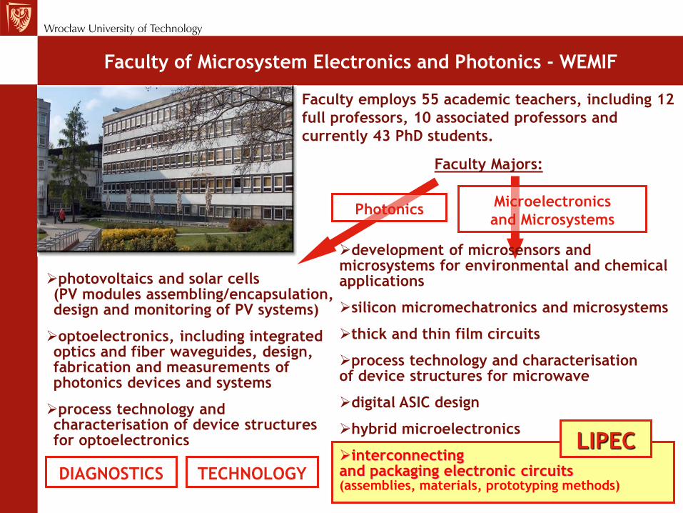
Faculty of Microsystem Electronics and Photonics - WEMIF
Faculty employs 55 academic teachers, including 12
full professors, 10 associated professors and
currently 43 PhD students.
Faculty Majors:
Microelectronics
and Microsystems
development of microsensors and microsystems for environmental and chemical applications
silicon micromechatronics and microsystems
thick and thin film circuits
process technology and characterisation of device structures for microwave
digital ASIC design
hybrid microelectronics
interconnecting and packaging electronic circuits(assemblies, materials, prototyping methods)
Photonics
photovoltaics and solar cells (PV modules assembling/encapsulation, design and monitoring of PV systems)
optoelectronics, including integrated optics and fiber waveguides, design, fabrication and measurements of photonics devices and systems
process technology and characterisation of device structures for optoelectronics
DIAGNOSTICS TECHNOLOGY
LIPEC
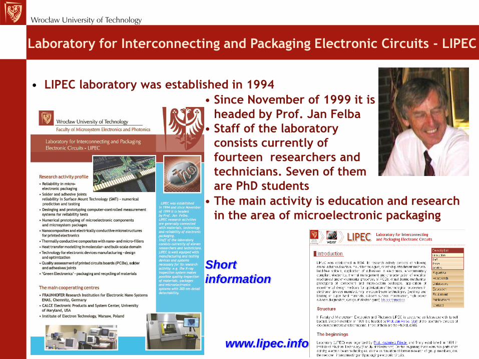
• LIPEC laboratory was established in 1994
www.lipec.info
Laboratory for Interconnecting and Packaging Electronic Circuits - LIPEC
• Since November of 1999 it is
headed by Prof. Jan Felba
• Staff of the laboratory
consists currently of
fourteen researchers and
technicians. Seven of them
are PhD students
• The main activity is education and research
in the area of microelectronic packaging
Short
information
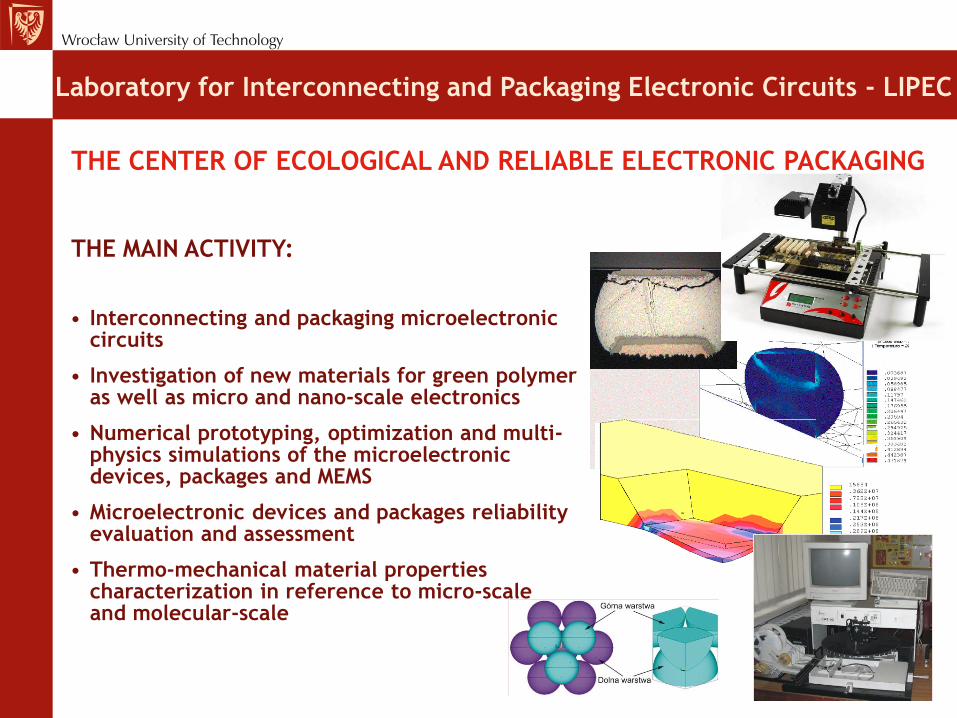
• Interconnecting and packaging microelectronic circuits
• Investigation of new materials for green polymer as well as micro and nano-scale electronics
• Numerical prototyping, optimization and multi-physics simulations of the microelectronic devices, packages and MEMS
• Microelectronic devices and packages reliability evaluation and assessment
• Thermo-mechanical material properties characterization in reference to micro-scale and molecular-scale
THE CENTER OF ECOLOGICAL AND RELIABLE ELECTRONIC PACKAGING
THE MAIN ACTIVITY:
Laboratory for Interconnecting and Packaging Electronic Circuits - LIPEC
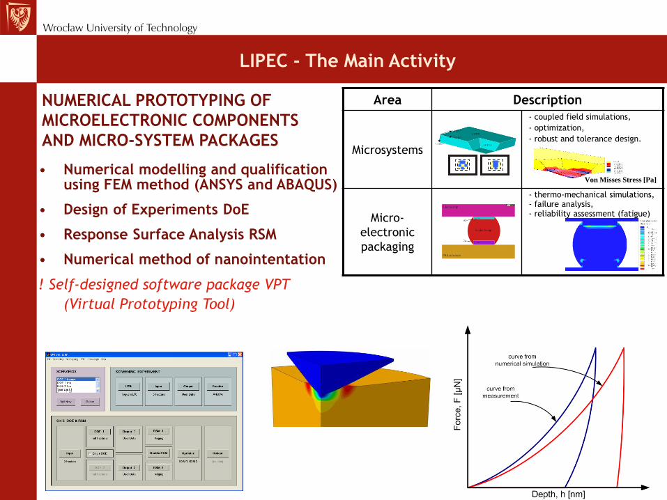
LIPEC - The Main Activity
Von Misses Stress [Pa]
Area Description
Microsystems
- coupled field simulations,
- optimization,
- robust and tolerance design.
Micro-
electronic
packaging
- thermo-mechanical simulations,- failure analysis,- reliability assessment (fatigue)
<110>
<110>
<100>
(100)
(111)
• Numerical modelling and qualification using FEM method (ANSYS and ABAQUS)
• Design of Experiments DoE
• Response Surface Analysis RSM
• Numerical method of nanointentation
! Self-designed software package VPT
(Virtual Prototyping Tool)
NUMERICAL PROTOTYPING OF
MICROELECTRONIC COMPONENTS
AND MICRO-SYSTEM PACKAGES
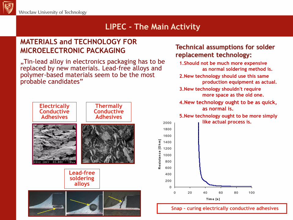
ElectricallyConductiveAdhesives
ThermallyConductiveAdhesives
MATERIALS and TECHNOLOGY FOR
MICROELECTRONIC PACKAGING
„Tin-lead alloy in electronics packaging has to be replaced by new materials. Lead-free alloys and polymer-based materials seem to be the most probable candidates”
Lead-free soldering
alloys0
200
400
600
800
1000
1200
1400
1600
1800
2000
0 20 40 60 80 100
Tim e [s ]
Re
sis
tan
ce
[O
hm
]
Snap – curing electrically conductive adhesives
1.Should not be much more expensive
as normal soldering method is.
2.New technology should use this same
production equipment as actual.
3.New technology shouldn't require
more space as the old one.
4.New technology ought to be as quick,
as normal is.
5.New technology ought to be more simply
like actual process is.
Technical assumptions for solder
replacement technology:
LIPEC - The Main Activity
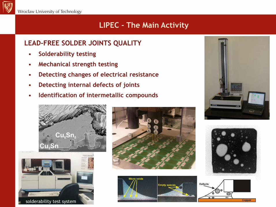
LEAD-FREE SOLDER JOINTS QUALITY
solderability test system
LIPEC - The Main Activity
• Solderability testing
• Mechanical strength testing
• Detecting changes of electrical resistance
• Detecting internal defects of joints
• Identification of intermetallic compounds
Silver Jum per
Adhesive
Join t
Strip
l
g
d
d
LIPEC - The Main Activity
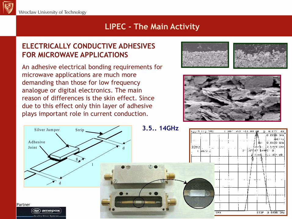
ELECTRICALLY CONDUCTIVE ADHESIVES
FOR MICROWAVE APPLICATIONS
An adhesive electrical bonding requirements for
microwave applications are much more
demanding than those for low frequency
analogue or digital electronics. The main
reason of differences is the skin effect. Since
due to this effect only thin layer of adhesive
plays important role in current conduction.
3.5.. 14GHz
Partner
LIPEC - The Main Activity
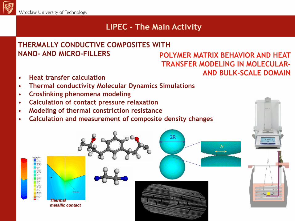
• Heat transfer calculation
• Thermal conductivity Molecular Dynamics Simulations
• Croslinking phenomena modeling
• Calculation of contact pressure relaxation
• Modeling of thermal constriction resistance
• Calculation and measurement of composite density changes
2R2R
2r
Thermal
metallic contact
POLYMER MATRIX BEHAVIOR AND HEAT
TRANSFER MODELING IN MOLECULAR-
AND BULK-SCALE DOMAIN
THERMALLY CONDUCTIVE COMPOSITES WITH
NANO- AND MICRO-FILLERS
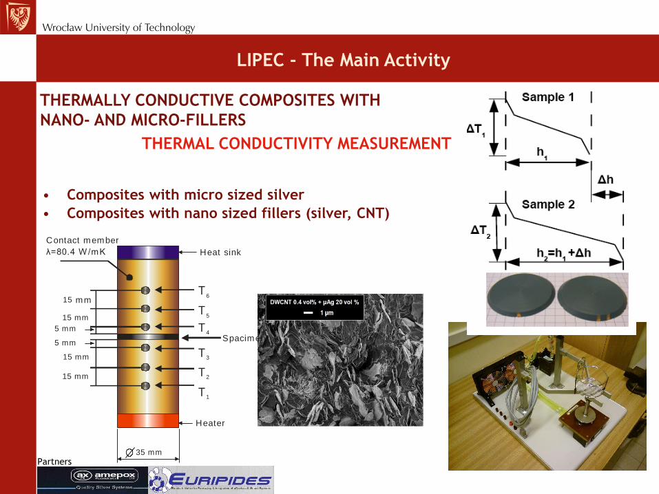
LIPEC - The Main Activity
• Composites with micro sized silver
• Composites with nano sized fillers (silver, CNT)
THERMALLY CONDUCTIVE COMPOSITES WITH
NANO- AND MICRO-FILLERS
T 1
T 2
T 3
T 4
T5
T6
15 mm
15 mm
15 mm
15 mm
5 mm
5 mm
Spacimen
35 mm
Heater
Heat sink
Contact member
λ=80.4 W/mK
Partners
THERMAL CONDUCTIVITY MEASUREMENT
LIPEC - The Main Activity
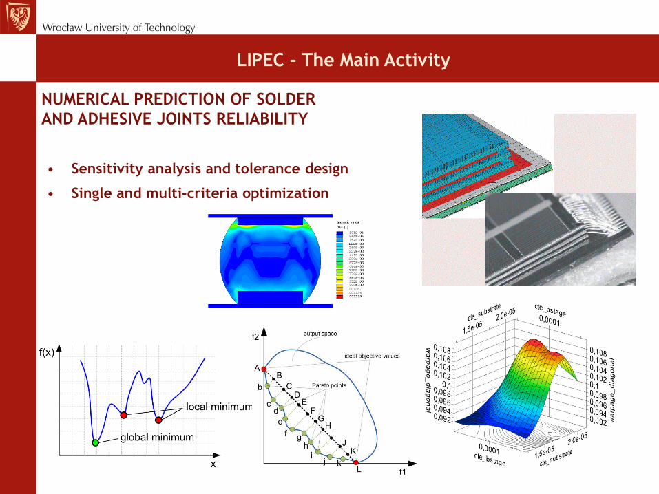
• Sensitivity analysis and tolerance design
• Single and multi-criteria optimization
NUMERICAL PREDICTION OF SOLDER
AND ADHESIVE JOINTS RELIABILITY
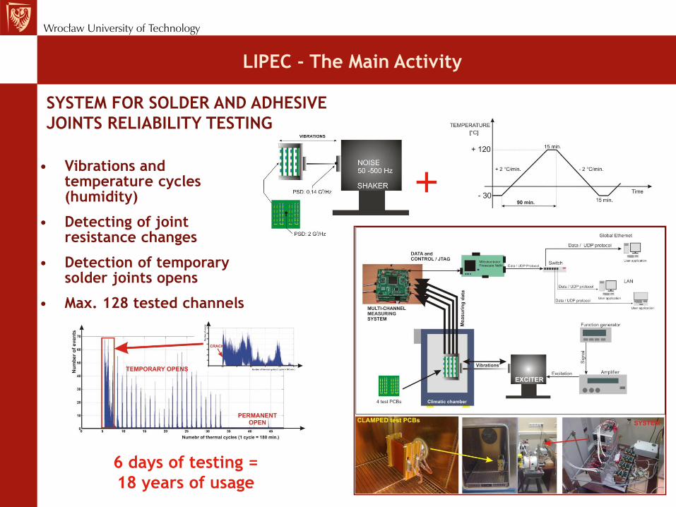
LIPEC - The Main Activity
SYSTEM FOR SOLDER AND ADHESIVE
JOINTS RELIABILITY TESTING
+
6 days of testing =
18 years of usage
• Vibrations and temperature cycles (humidity)
• Detecting of joint resistance changes
• Detection of temporary solder joints opens
• Max. 128 tested channels
LIPEC - The Main Activity
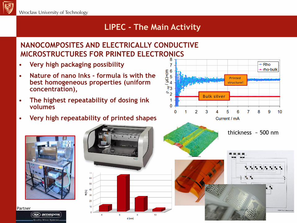
NANOCOMPOSITES AND ELECTRICALLY CONDUCTIVE
MICROSTRUCTURES FOR PRINTED ELECTRONICS
• Very high packaging possibility
• Nature of nano Inks - formula is with the best homogeneous properties (uniform concentration),
• The highest repeatability of dosing ink volumes
• Very high repeatability of printed shapes
Printed
structure!
Bulk silver
Partner
thickness ~ 500 nm
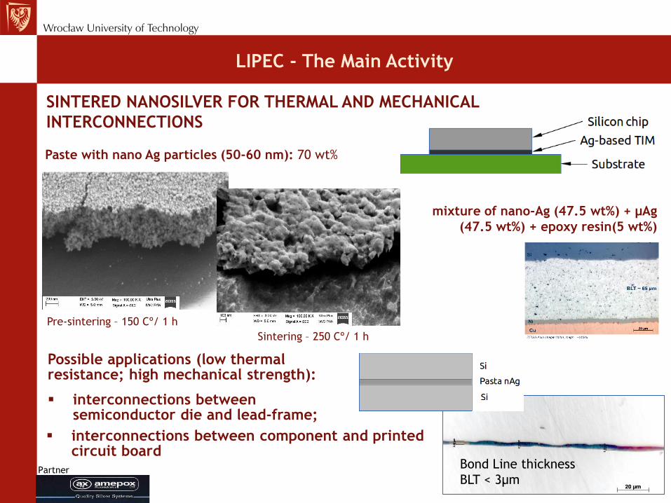
LIPEC - The Main Activity
SINTERED NANOSILVER FOR THERMAL AND MECHANICAL
INTERCONNECTIONS
Partner
Paste with nano Ag particles (50-60 nm): 70 wt%
Pre-sintering – 150 Cº/ 1 h
Sintering – 250 Cº/ 1 h
Bond Line thickness
BLT < 3µm
mixture of nano-Ag (47.5 wt%) + µAg
(47.5 wt%) + epoxy resin(5 wt%)
Possible applications (low thermalresistance; high mechanical strength):
interconnections between semiconductor die and lead-frame;
interconnections between component and printedcircuit board
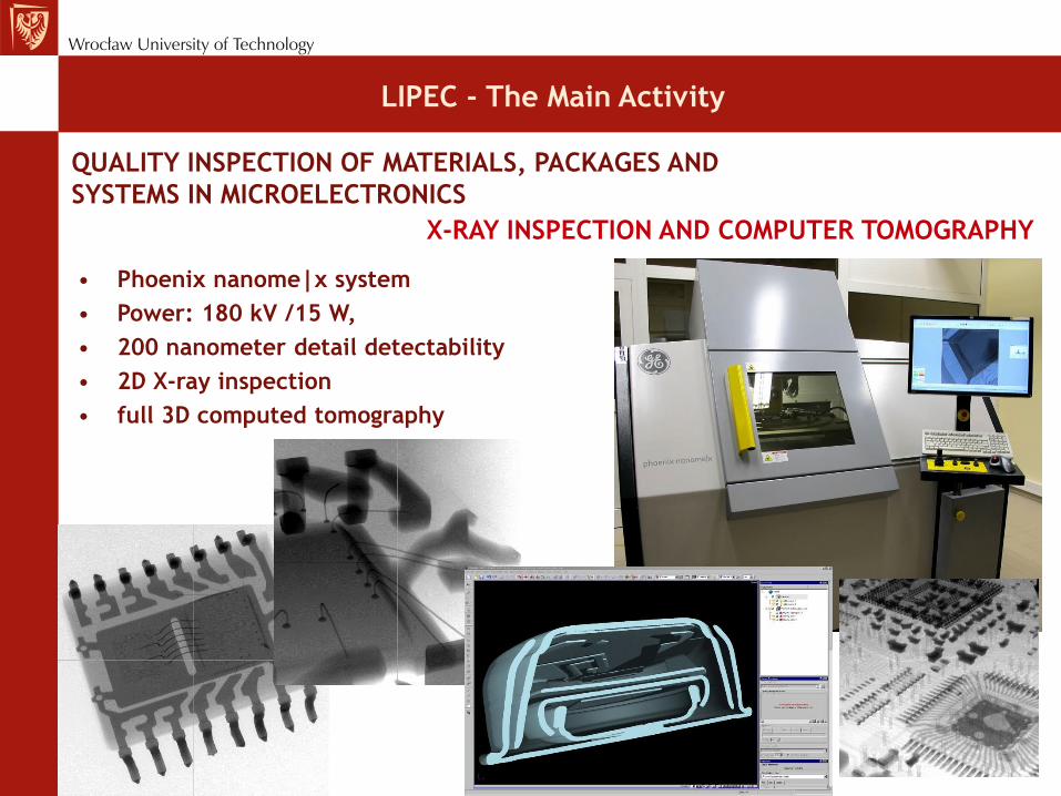
QUALITY INSPECTION OF MATERIALS, PACKAGES AND
SYSTEMS IN MICROELECTRONICS
LIPEC - The Main Activity
• Phoenix nanome|x system
• Power: 180 kV /15 W,
• 200 nanometer detail detectability
• 2D X-ray inspection
• full 3D computed tomography
X-RAY INSPECTION AND COMPUTER TOMOGRAPHY
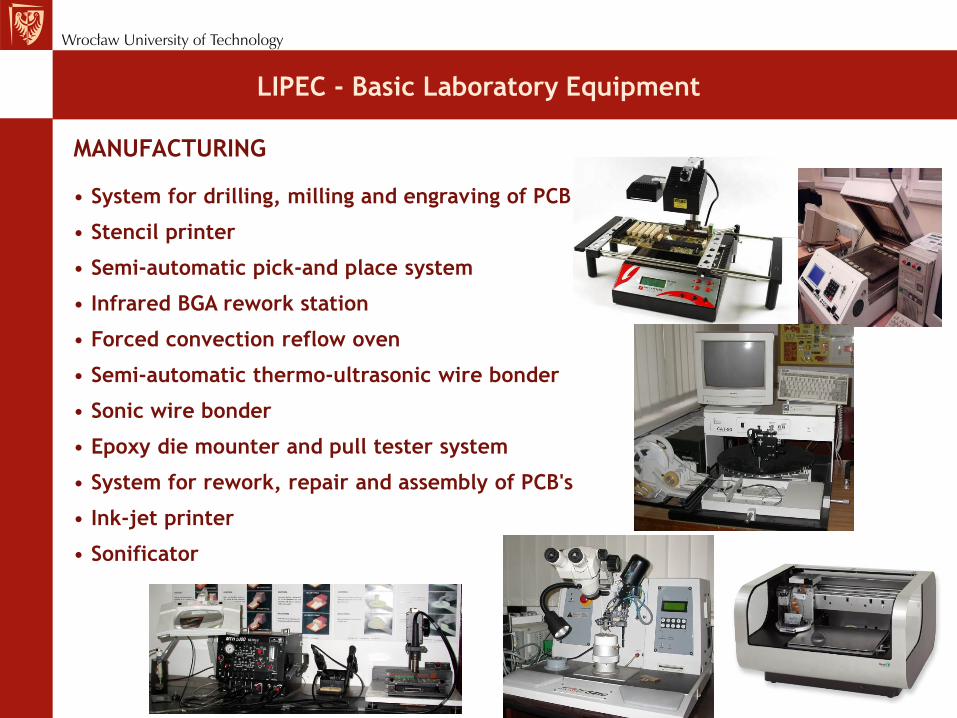
• System for drilling, milling and engraving of PCB
• Stencil printer
• Semi-automatic pick-and place system
• Infrared BGA rework station
• Forced convection reflow oven
• Semi-automatic thermo-ultrasonic wire bonder
• Sonic wire bonder
• Epoxy die mounter and pull tester system
• System for rework, repair and assembly of PCB's
• Ink-jet printer
• Sonificator
LIPEC - Basic Laboratory Equipment
MANUFACTURING
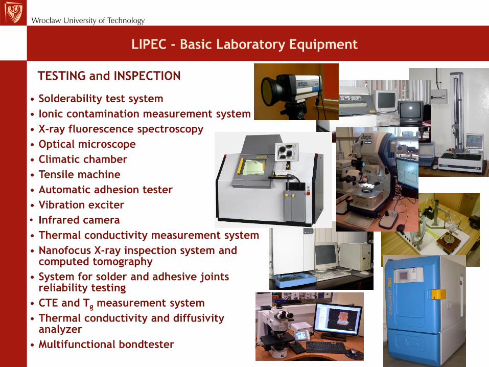
• Solderability test system
• Ionic contamination measurement system
• X-ray fluorescence spectroscopy
• Optical microscope
• Climatic chamber
• Tensile machine
• Automatic adhesion tester
• Vibration exciter
• Infrared camera
• Thermal conductivity measurement system
• Nanofocus X-ray inspection system andcomputed tomography
• System for solder and adhesive joints reliability testing
• CTE and Tg measurement system
• Thermal conductivity and diffusivity analyzer
• Multifunctional bondtester
LIPEC - Basic Laboratory Equipment
TESTING and INSPECTION
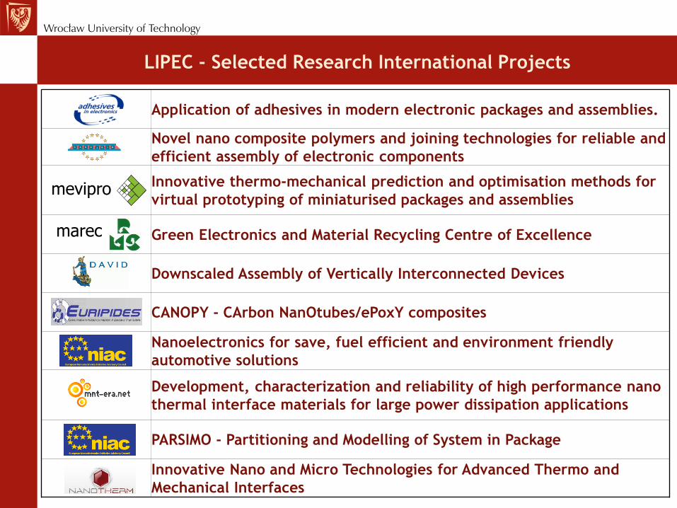
Application of adhesives in modern electronic packages and assemblies.
Novel nano composite polymers and joining technologies for reliable and
efficient assembly of electronic components
Innovative thermo-mechanical prediction and optimisation methods for
virtual prototyping of miniaturised packages and assemblies
Green Electronics and Material Recycling Centre of Excellence
Downscaled Assembly of Vertically Interconnected Devices
CANOPY - CArbon NanOtubes/ePoxY composites
Nanoelectronics for save, fuel efficient and environment friendly
automotive solutions
Development, characterization and reliability of high performance nano
thermal interface materials for large power dissipation applications
PARSIMO - Partitioning and Modelling of System in Package
Innovative Nano and Micro Technologies for Advanced Thermo and
Mechanical Interfaces
LIPEC - Selected Research International Projects
mevipro
marec
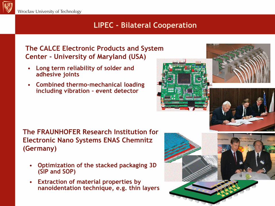
LIPEC - Bilateral Cooperation
• Long term reliability of solder and adhesive joints
• Combined thermo-mechanical loading including vibration – event detector
The CALCE Electronic Products and System
Center - University of Maryland (USA)
• Optimization of the stacked packaging 3D (SIP and SOP)
• Extraction of material properties by nanoidentation technique, e.g. thin layers
The FRAUNHOFER Research Institution for
Electronic Nano Systems ENAS Chemnitz
(Germany)
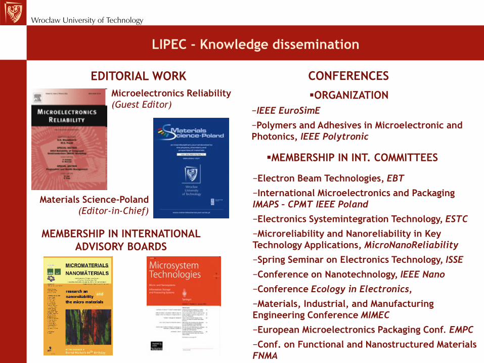
LIPEC - Knowledge dissemination
CONFERENCESEDITORIAL WORK
Microelectronics Reliability
(Guest Editor)
Materials Science-Poland
(Editor-in-Chief)
MEMBERSHIP IN INTERNATIONAL
ADVISORY BOARDS
ORGANIZATION
MEMBERSHIP IN INT. COMMITTEES
−IEEE EuroSimE
−Polymers and Adhesives in Microelectronic and
Photonics, IEEE Polytronic
−Electron Beam Technologies, EBT
−International Microelectronics and Packaging
IMAPS – CPMT IEEE Poland
−Electronics Systemintegration Technology, ESTC
−Microreliability and Nanoreliability in Key
Technology Applications, MicroNanoReliability
−Spring Seminar on Electronics Technology, ISSE
−Conference on Nanotechnology, IEEE Nano
−Conference Ecology in Electronics‚
−Materials, Industrial, and Manufacturing
Engineering Conference MIMEC
−European Microelectronics Packaging Conf. EMPC
−Conf. on Functional and Nanostructured Materials
FNMA
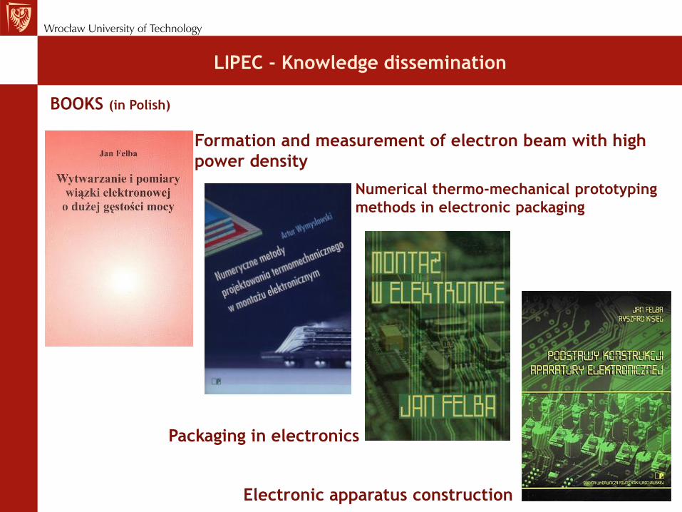
LIPEC - Knowledge dissemination
BOOKS (in Polish)
Electronic apparatus construction
Packaging in electronics
Numerical thermo-mechanical prototyping
methods in electronic packaging
Formation and measurement of electron beam with high
power density
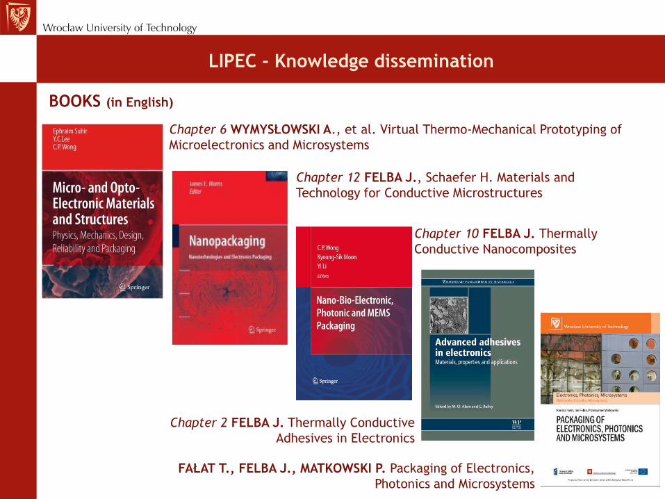
LIPEC - Knowledge dissemination
BOOKS (in English)
Chapter 6 WYMYSŁOWSKI A., et al. Virtual Thermo-Mechanical Prototyping of
Microelectronics and Microsystems
Chapter 12 FELBA J., Schaefer H. Materials and
Technology for Conductive Microstructures
Chapter 10 FELBA J. Thermally
Conductive Nanocomposites
Chapter 2 FELBA J. Thermally Conductive
Adhesives in Electronics
FAŁAT T., FELBA J., MATKOWSKI P. Packaging of Electronics,
Photonics and Microsystems
LIPEC - Knowledge dissemination
BOOKS (in English)
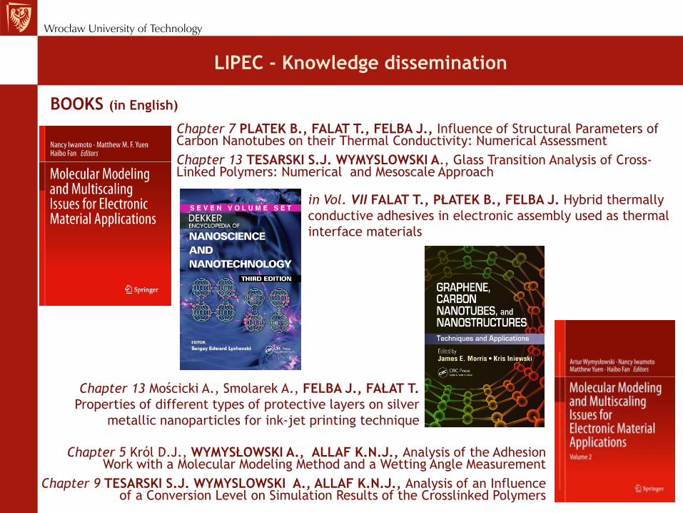
Chapter 13 Mościcki A., Smolarek A., FELBA J., FAŁAT T.
Properties of different types of protective layers on silver
metallic nanoparticles for ink-jet printing technique
Chapter 7 PLATEK B., FALAT T., FELBA J., Influence of Structural Parameters of Carbon Nanotubes on their Thermal Conductivity: Numerical Assessment
Chapter 13 TESARSKI S.J. WYMYSLOWSKI A., Glass Transition Analysis of Cross-Linked Polymers: Numerical and Mesoscale Approach
in Vol. VII FALAT T., PŁATEK B., FELBA J. Hybrid thermally
conductive adhesives in electronic assembly used as thermal
interface materials
Chapter 5 Król D.J., WYMYSŁOWSKI A., ALLAF K.N.J., Analysis of the Adhesion Work with a Molecular Modeling Method and a Wetting Angle Measurement
Chapter 9 TESARSKI S.J. WYMYSLOWSKI A., ALLAF K.N.J., Analysis of an Influence of a Conversion Level on Simulation Results of the Crosslinked Polymers