lab07 lecture
TRANSCRIPT
8/2/2019 Lab07 Lecture
http://slidepdf.com/reader/full/lab07-lecture 1/6
ECE238 laboratory lecture notes University of New Mexico
1
Lecture notes - Introduction to Accumulators andFPGAs
Accumulator Basics
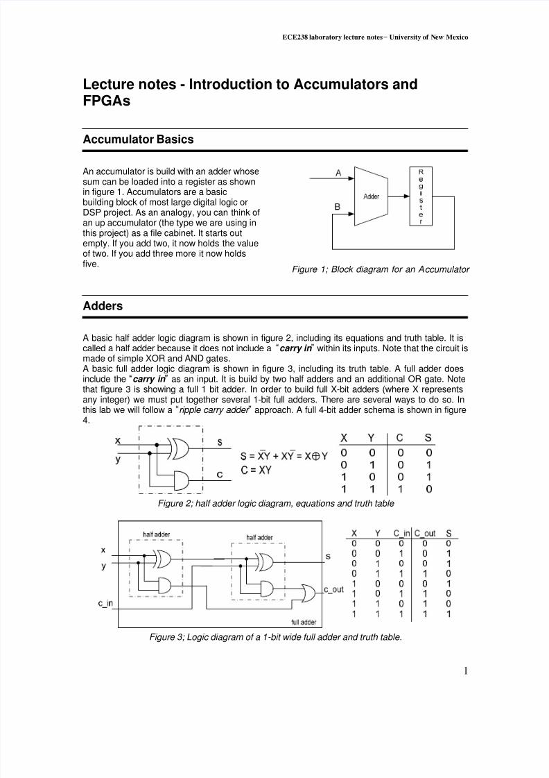
An accumulator is build with an adder whosesum can be loaded into a register as shownin figure 1. Accumulators are a basicbuilding block of most large digital logic orDSP project. As an analogy, you can think ofan up accumulator (the type we are using inthis project) as a file cabinet. It starts outempty. If you add two, it now holds the valueof two. If you add three more it now holdsfive.
Figure 1; Block diagram for an Accumulator
Adders
A basic half adder logic diagram is shown in figure 2, including its equations and truth table. It iscalled a half adder because it does not include a carry in within its inputs. Note that the circuit ismade of simple XOR and AND gates. A basic full adder logic diagram is shown in figure 3, including its truth table. A full adder doesinclude the carry in as an input. It is build by two half adders and an additional OR gate. Notethat figure 3 is showing a full 1 bit adder. In order to build full X-bit adders (where X representsany integer) we must put together several 1-bit full adders. There are several ways to do so. In
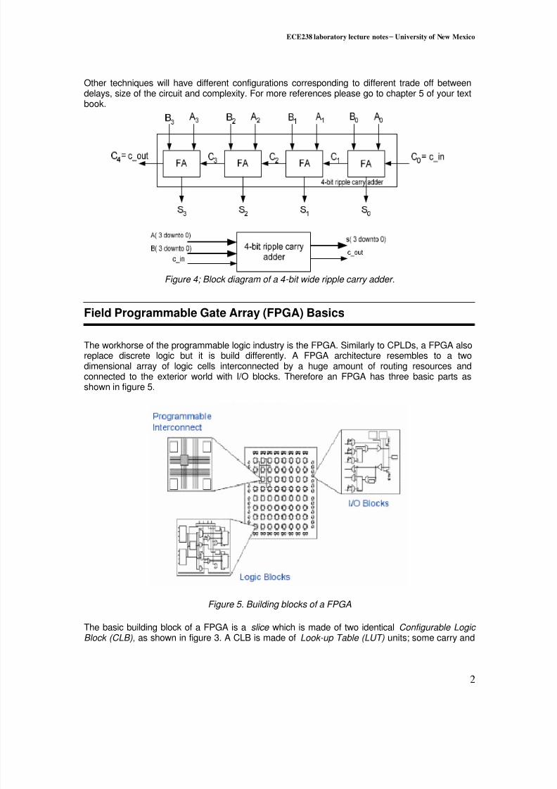
this lab we will follow a ripple carry adder approach. A full 4-bit adder schema is shown in figure4.
Figure 2 ; half adder logic diagram, equations and truth table
Figure 3 ; Logic diagram of a 1- bit wide full adder and truth table.
8/2/2019 Lab07 Lecture
http://slidepdf.com/reader/full/lab07-lecture 2/6
ECE238 laboratory lecture notes University of New Mexico
2
Other techniques will have different configurations corresponding to different trade off betweendelays, size of the circuit and complexity. For more references please go to chapter 5 of your textbook.
Figure 4 ; Block diagram of a 4 - bit wide ripple carry adder.
Field Programmable Gate Array (FPGA) Basics
The workhorse of the programmable logic industry is the FPGA. Similarly to CPLDs, a FPGA alsoreplace discrete logic but it is build differently. A FPGA architecture resembles to a twodimensional array of logic cells interconnected by a huge amount of routing resources andconnected to the exterior world with I/O blocks. Therefore an FPGA has three basic parts asshown in figure 5.
Figure 5. Building blocks of a FPGA
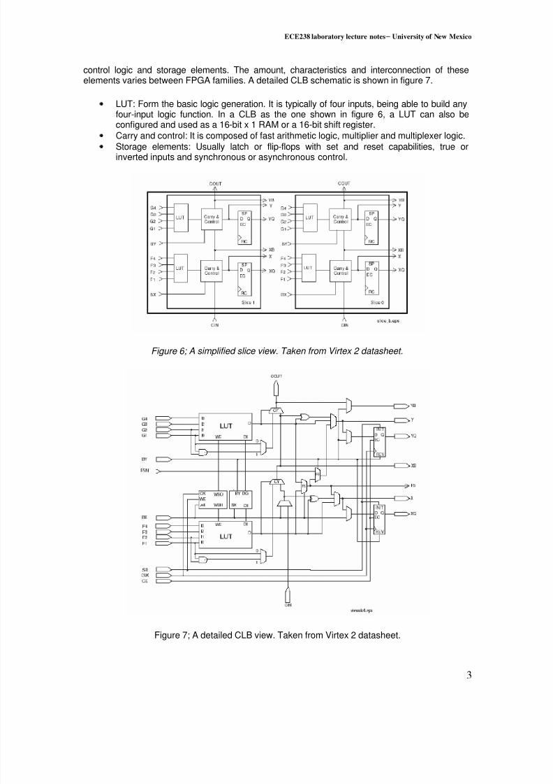
The basic building block of a FPGA is a slice which is made of two identical Configurable Logic Block (CLB), as shown in figure 3. A CLB is made of Look -up Table (LUT) units; some carry and
8/2/2019 Lab07 Lecture
http://slidepdf.com/reader/full/lab07-lecture 3/6
ECE238 laboratory lecture notes University of New Mexico
3
control logic and storage elements. The amount, characteristics and interconnection of theseelements varies between FPGA families. A detailed CLB schematic is shown in figure 7.
LUT: Form the basic logic generation. It is typically of four inputs, being able to build anyfour-input logic function. In a CLB as the one shown in figure 6, a LUT can also beconfigured and used as a 16-bit x 1 RAM or a 16-bit shift register.
Carry and control: It is composed of fast arithmetic logic, multiplier and multiplexer logic. Storage elements: Usually latch or flip-flops with set and reset capabilities, true orinverted inputs and synchronous or asynchronous control.
Figure 6 ; A simplified slice view. Taken from Virtex 2 datasheet.
Figure 7; A detailed CLB view. Taken from Virtex 2 datasheet.
8/2/2019 Lab07 Lecture
http://slidepdf.com/reader/full/lab07-lecture 4/6
ECE238 laboratory lecture notes University of New Mexico
4
For you to have an idea of how much logic we can fit in the chips on the boards we will use for,note that they have around 400 CLBs. It is also common to measure a FPGA size by useable orsystem gates. If you remember the work you did earlier in the semester with the 7400 chip youwill recall that the chip contained four two input NAND gates. Given the belief that any logic can
be developed using enough two input NAND gates, this measure has been assigned theuseable/system gates term. The Digilent boards (containing the Xilinx SpartanXL FPGA chips) wewill be using for the rest of the semester are described as having 10 thousand useable gates.
Each day, the number of useable gates increases, as does the speed. What is the standard todaywill be considered antique in the next year or so. The one underlying theme that will continue tosurvive is the coding scheme. You can use VHDL to program ANY CPLD and ANY FPGA. That iswhy hardware description languages are critical to know.
Finally, a significant difference with CPLDs is that a FPGA is a SRAM device, it requires externaldevices for configuration after each power cycle. In general, FPGAs offer more logic flexibility andmore sophisticated system features than CPLDs: clock management, on-chip RAM, DSPfunctions (multipliers), etc. Why can say that FPGA are generally used for larger and more
complex designs. Be aware tough, that they consume a lot more power than a CPLD.
Using the Digilent XL Prototyping Board
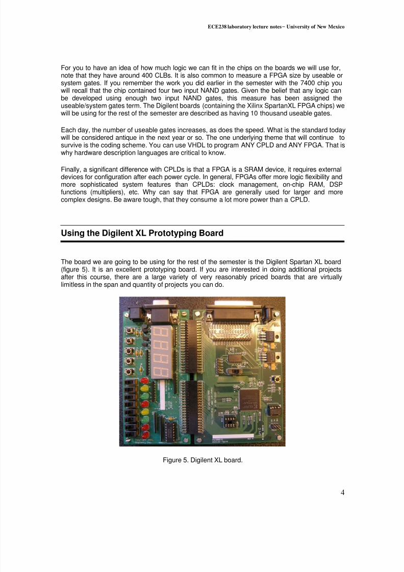
The board we are going to be using for the rest of the semester is the Digilent Spartan XL board(figure 5). It is an excellent prototyping board. If you are interested in doing additional projectsafter this course, there are a large variety of very reasonably priced boards that are virtuallylimitless in the span and quantity of projects you can do.
Figure 5. Digilent XL board.
8/2/2019 Lab07 Lecture
http://slidepdf.com/reader/full/lab07-lecture 5/6
ECE238 laboratory lecture notes University of New Mexico
5
The Xilinx FPGA on the board is a 3.3volt, 10,000 useable gate device. Once again you can seewhere we are using lower voltages (3.3 vs. the 5 from the discrete logic) to conserve power andheat. The trend is towards lower and lower voltages in programmable logic. The device has aspeed grade of 5. This is the 5C that you see at the bottom of the chip. A large number of thesechips are cut at a single time from a large wafer. The chips closer to the center of the wafer are ofbetter quality and their speed is higher (thus a higher number and price). The lower the numberthe further from the center of the wafer and thus the slower the device (and cheaper the cost). Forour chip (XC2S30), they come in speed grades 4 and 5.
We will also begin using more and more files within each project. This is necessary anytime youwish to increase your level of complexity and increase the quantity of things you wish toaccomplish.
Floorplanner
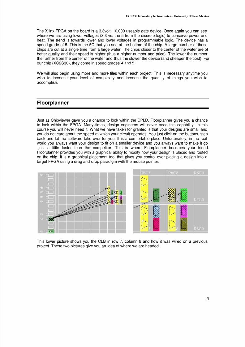
Just as Chipviewer gave you a chance to look within the CPLD, Floorplanner gives you a chanceto look within the FPGA. Many times, design engineers will never need this capability. In thiscourse you will never need it. What we have taken for granted is that your designs are small andyou do not care about the speed at which your circuit operates. You just click on the buttons, stepback and let the software take over for you. It is a comfortable place. Unfortunately, in the realworld you always want your design to fit on a smaller device and you always want to make it go
just a little faster than the competitor. This is where Floorplanner becomes your friend.Floorplanner provides you with a graphical ability to modify how your design is placed and routedon the chip. It is a graphical placement tool that gives you control over placing a design into atarget FPGA using a drag and drop paradigm with the mouse pointer.
This lower picture shows you the CLB in row 7, column 8 and how it was wired on a previousproject. These two pictures give you an idea of where we are headed.
8/2/2019 Lab07 Lecture
http://slidepdf.com/reader/full/lab07-lecture 6/6
This document was created with Win2PDF available at http://www.daneprairie.com.The unregistered version of Win2PDF is for evaluation or non-commercial use only.