lab manual “silvaco atlas – device simulation software”
TRANSCRIPT
LAB MANUAL
“Silvaco ATLAS – DeviceSimulation Software”
Centre for Detector & Related Software Technology(CDRST)
Department of Physics & Astrophysics, University of Delhi
1
INDEX
1. OVERVIEW………………………………………………....3
2. ABOUT SILICON DETECTOR………………………...…4
2.1 Silicon tracker of CMS at LHC……………………………4 2.2 Radiation Damage………………………….………...........5
3. SILVACO SIMULATION ENVIRONMENT USED FOR SILICON DETECTOR……………………………………....6
4.ATLAS OVERVIEW …………………..…………....…..…...7
5. DECKBUILD OVERVIEW…………….…………….……..8
6. DEV-EDIT OVERVIEW……………………….……..……..9
7. DEVICE BASIC CONSTRUCTION LAYOUT.…………10
7.1 Mesh Construction……………………………………..10 7.2. Regions…………………………………………………11
7.3. Electrodes………………………………………….…...117.4. Doping………………………………………………….127.5. Material…………………………………………….…..127.6. Models………………………………………………….127.7. Solution Method……………………………………….137.8. Solution Specification………………………………....147.9. Data Extraction And Plotting………………………...15
8. DEMO EXAMPLE: CREATING A TWO DIMENSIONAL PAD DIODE STRUCTURE…………….…………………16
REFERENCES
2
1. OVERVIEW
The construction of experimental specimens is the process followed by most research centers
and manufacturers of Silicon detectors. Although it is the most reliable procedure for
evaluating the performance of a detector cell, it is still costly and time consuming. On the
other hand, modeling using software provides a fast, consistent, and relatively inexpensive
way to design silicon detectors. Modeling and simulation allows for thousands of
combinations to be investigated before the fabrication of actual examples. Here we use of
Silvaco ATLASTM simulation software to model a Silicon Detector cell and evaluate the
performance for different variations of cell parameters. Silvaco TCAD tool is a widely used
software package for the simulation of various type of Si devices.
2. ABOUT SILICON DETECTOR
Particle detectors are devices, or instruments that can detect track, momentum, energy, etc. of
the incident particles. There are 3 types of detectors: solid, liquid, gas. Our study is focused
on solid semiconductor silicon detectors because of various advantages over liquid and
gaseous detectors. The energy required for the generation of electron hole pairs is
comparatively smaller. These have high density of atoms and therefore are compact. They
have a smaller size and can be carried easily from one place to another. Silicon is chosen
because it is easily available and its natural oxide can act as both insulating and passivating
layers. It can be operated at room temperature. Also it has a developed electronics
technology.
A pn junction is formed by diffusing p-type impurities on a n-type wafer or vice versa. The
majority carriers (electrons in n-type, holes in p-type) diffuse to the other side because of the
density gradient, leaving behind ions. This region of positive and negative ions formed is
called depletion region. The electric field and the potential developed in this region can be
calculated using the Poisson’s equation. Also the depletion width can be calculated. The
diagrammatical view is shown in Figure 1.
The above theory has been generated from [R1, R2, R3, R4].
3
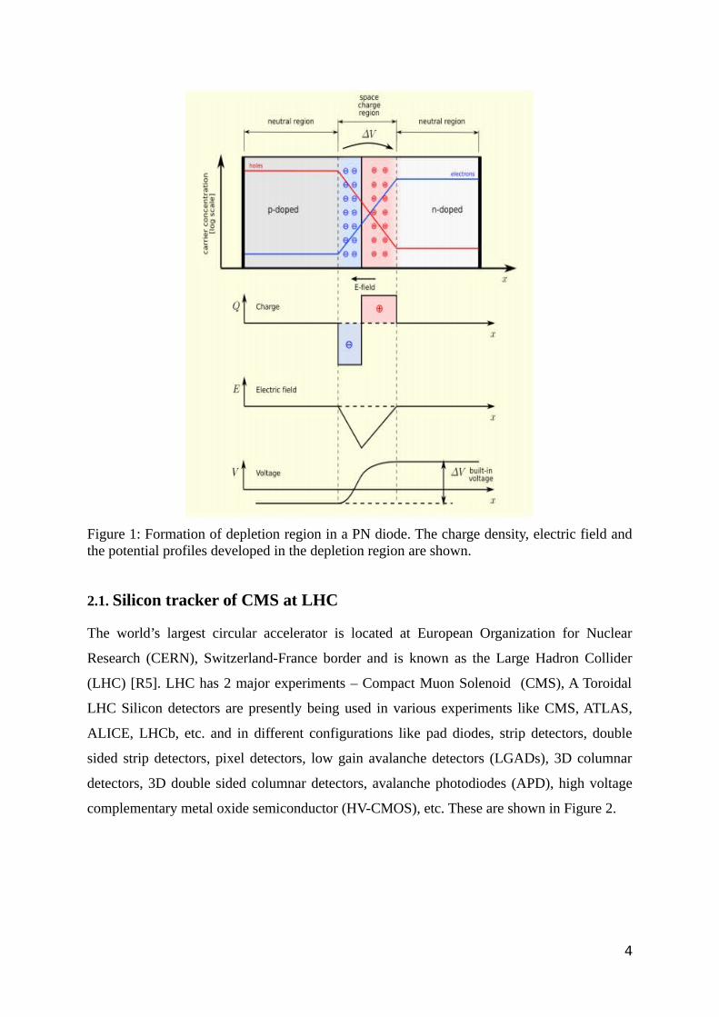
Figure 1: Formation of depletion region in a PN diode. The charge density, electric field andthe potential profiles developed in the depletion region are shown.
2.1. Silicon tracker of CMS at LHC
The world’s largest circular accelerator is located at European Organization for Nuclear
Research (CERN), Switzerland-France border and is known as the Large Hadron Collider
(LHC) [R5]. LHC has 2 major experiments – Compact Muon Solenoid (CMS), A Toroidal
LHC Silicon detectors are presently being used in various experiments like CMS, ATLAS,
ALICE, LHCb, etc. and in different configurations like pad diodes, strip detectors, double
sided strip detectors, pixel detectors, low gain avalanche detectors (LGADs), 3D columnar
detectors, 3D double sided columnar detectors, avalanche photodiodes (APD), high voltage
complementary metal oxide semiconductor (HV-CMOS), etc. These are shown in Figure 2.
4
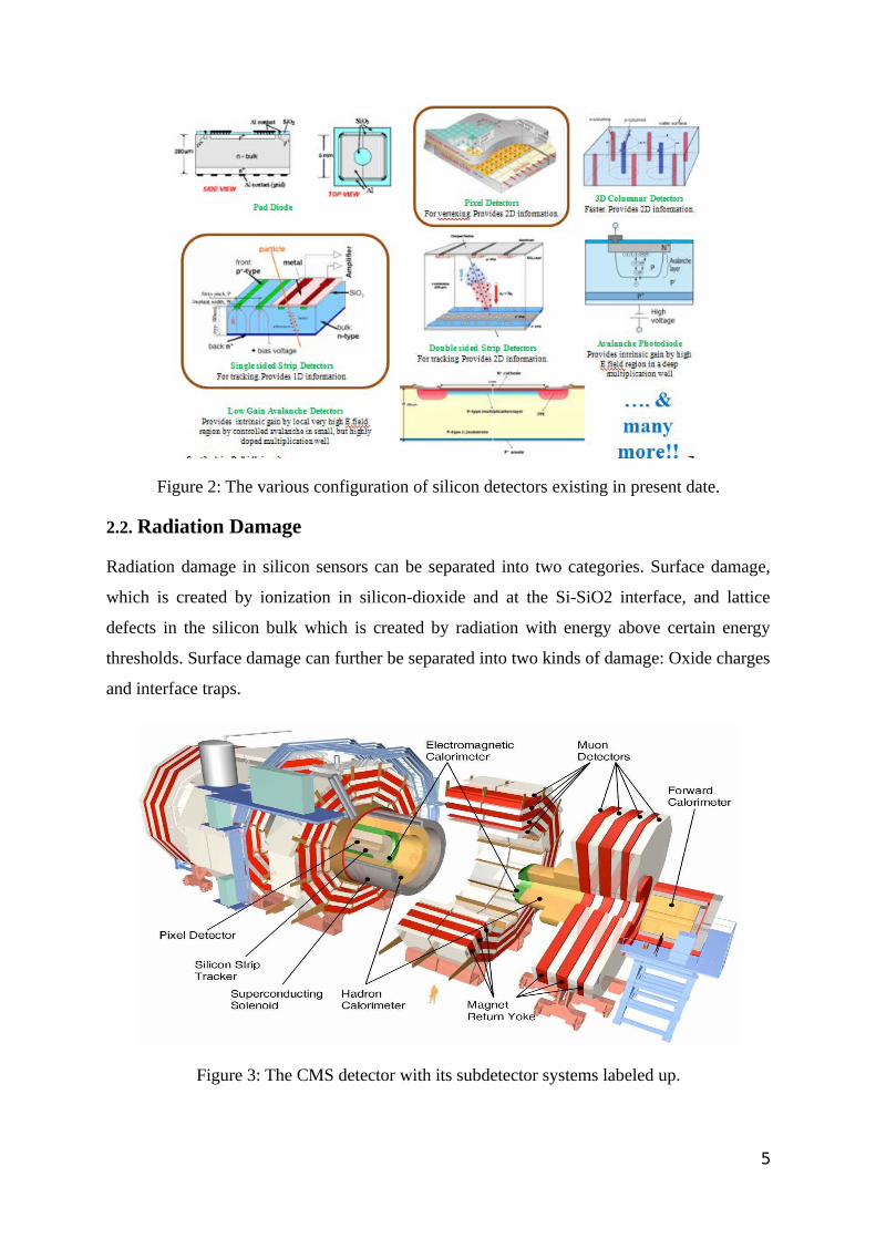
Figure 2: The various configuration of silicon detectors existing in present date.
2.2. Radiation Damage
Radiation damage in silicon sensors can be separated into two categories. Surface damage,
which is created by ionization in silicon-dioxide and at the Si-SiO2 interface, and lattice
defects in the silicon bulk which is created by radiation with energy above certain energy
thresholds. Surface damage can further be separated into two kinds of damage: Oxide charges
and interface traps.
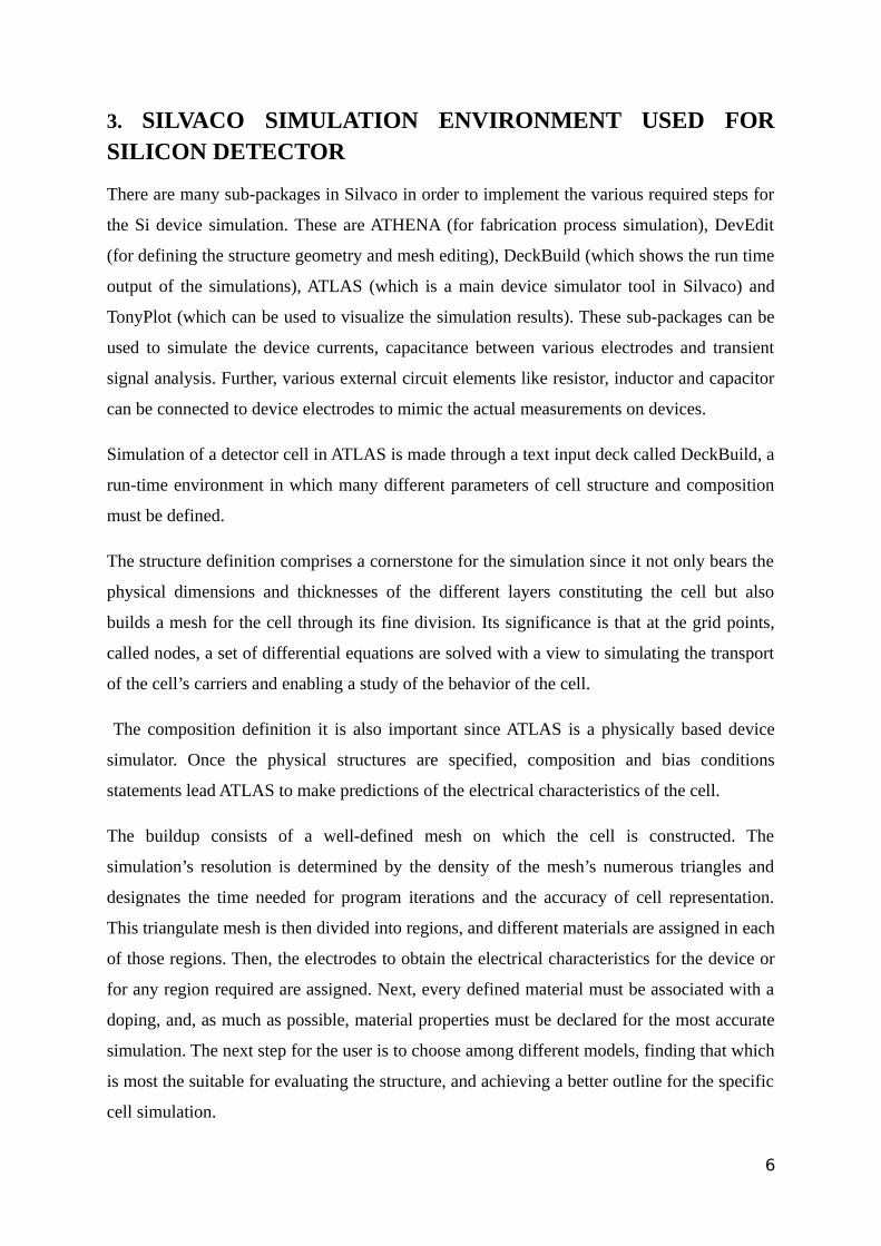
Figure 3: The CMS detector with its subdetector systems labeled up.
5
3. SILVACO SIMULATION ENVIRONMENT USED FORSILICON DETECTOR
There are many sub-packages in Silvaco in order to implement the various required steps for
the Si device simulation. These are ATHENA (for fabrication process simulation), DevEdit
(for defining the structure geometry and mesh editing), DeckBuild (which shows the run time
output of the simulations), ATLAS (which is a main device simulator tool in Silvaco) and
TonyPlot (which can be used to visualize the simulation results). These sub-packages can be
used to simulate the device currents, capacitance between various electrodes and transient
signal analysis. Further, various external circuit elements like resistor, inductor and capacitor
can be connected to device electrodes to mimic the actual measurements on devices.
Simulation of a detector cell in ATLAS is made through a text input deck called DeckBuild, a
run-time environment in which many different parameters of cell structure and composition
must be defined.
The structure definition comprises a cornerstone for the simulation since it not only bears the
physical dimensions and thicknesses of the different layers constituting the cell but also
builds a mesh for the cell through its fine division. Its significance is that at the grid points,
called nodes, a set of differential equations are solved with a view to simulating the transport
of the cell’s carriers and enabling a study of the behavior of the cell.
The composition definition it is also important since ATLAS is a physically based device
simulator. Once the physical structures are specified, composition and bias conditions
statements lead ATLAS to make predictions of the electrical characteristics of the cell.
The buildup consists of a well-defined mesh on which the cell is constructed. The
simulation’s resolution is determined by the density of the mesh’s numerous triangles and
designates the time needed for program iterations and the accuracy of cell representation.
This triangulate mesh is then divided into regions, and different materials are assigned in each
of those regions. Then, the electrodes to obtain the electrical characteristics for the device or
for any region required are assigned. Next, every defined material must be associated with a
doping, and, as much as possible, material properties must be declared for the most accurate
simulation. The next step for the user is to choose among different models, finding that which
is most the suitable for evaluating the structure, and achieving a better outline for the specific
cell simulation.
6
A specification of different particles (MIP, LASER) illuminates the cell as in real conditions,
simulating different regions of the detector cell, depending on the beam chosen. Also, the
selection of a method, among the different offered by the ATLASTM library, is needed for
solving the differential equations through which the cell’s operating characteristics arise.
These characteristics from the simulation can be saved in a log file and used to create plots
using TONYPLOT, the interactive graphics and analysis package included in the program.
The preceding analysis of cell buildup is illustrated in Figure 1
4. ATLAS OVERVIEW
Atlas provides general capabilities for physically-based two (2D) and three-dimensional (3D)
simulation of semiconductor devices. It predicts the electrical behavior of specified
semiconductor structures and provides insight into the internal physical mechanisms
associated with device operation.
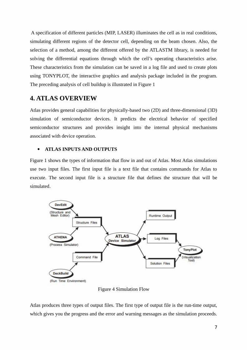
ATLAS INPUTS AND OUTPUTS
Figure 1 shows the types of information that flow in and out of Atlas. Most Atlas simulations
use two input files. The first input file is a text file that contains commands for Atlas to
execute. The second input file is a structure file that defines the structure that will be
simulated.
Figure 4 Simulation Flow
Atlas produces three types of output files. The first type of output file is the run-time output,
which gives you the progress and the error and warning messages as the simulation proceeds.
7
The second type of output file is the log file, which stores all terminal voltages and currents
from the device analysis. The third type of output file is the solution file, which stores 2D and
3D data relating to the values of solution variables within the device at a given bias point.
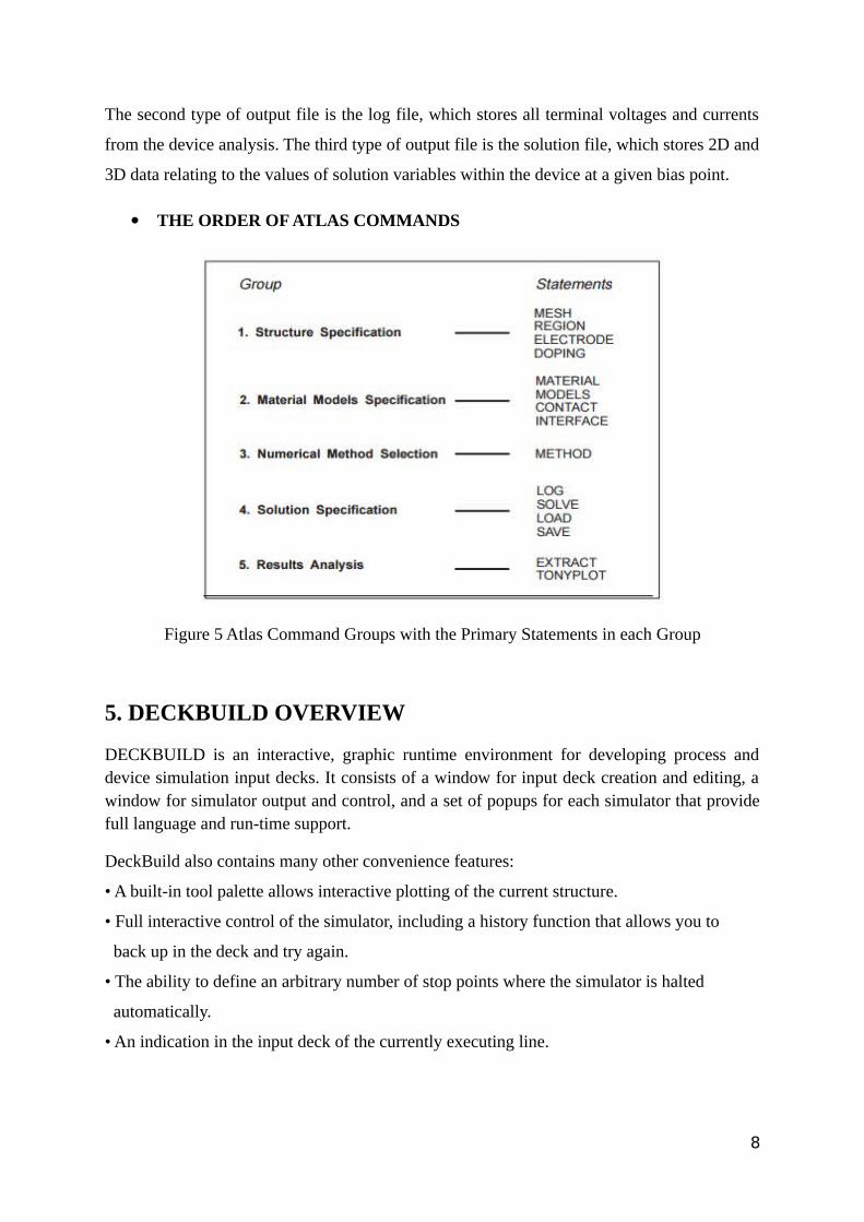
THE ORDER OF ATLAS COMMANDS
Figure 5 Atlas Command Groups with the Primary Statements in each Group
5. DECKBUILD OVERVIEW
DECKBUILD is an interactive, graphic runtime environment for developing process anddevice simulation input decks. It consists of a window for input deck creation and editing, awindow for simulator output and control, and a set of popups for each simulator that providefull language and run-time support.
DeckBuild also contains many other convenience features:
• A built-in tool palette allows interactive plotting of the current structure.
• Full interactive control of the simulator, including a history function that allows you to
back up in the deck and try again.
• The ability to define an arbitrary number of stop points where the simulator is halted
automatically.
• An indication in the input deck of the currently executing line.
8
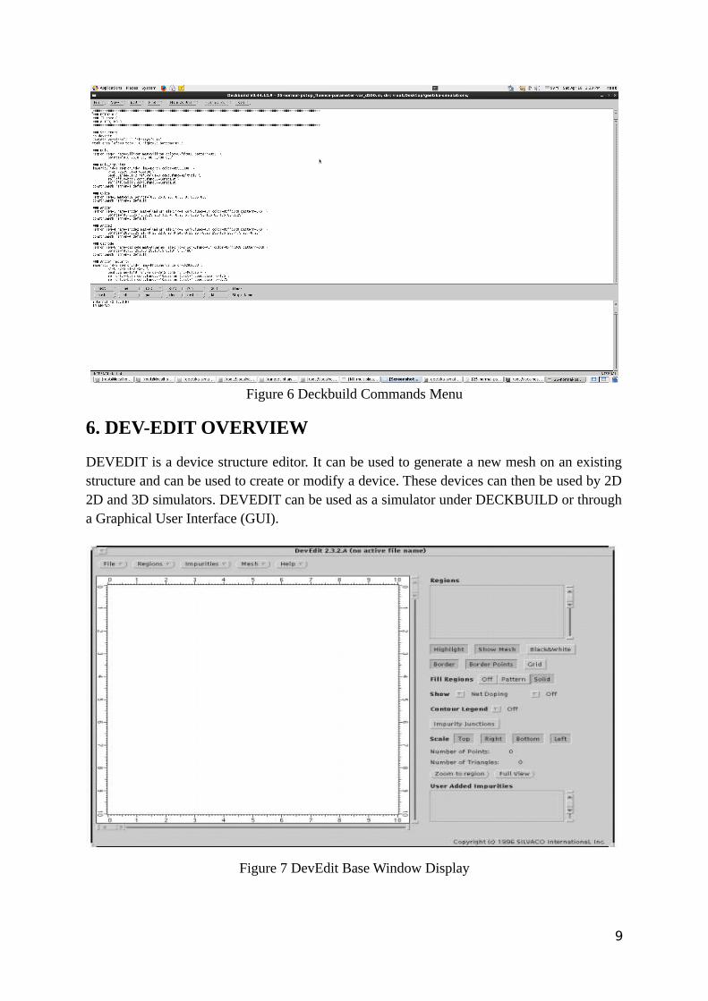
Figure 6 Deckbuild Commands Menu
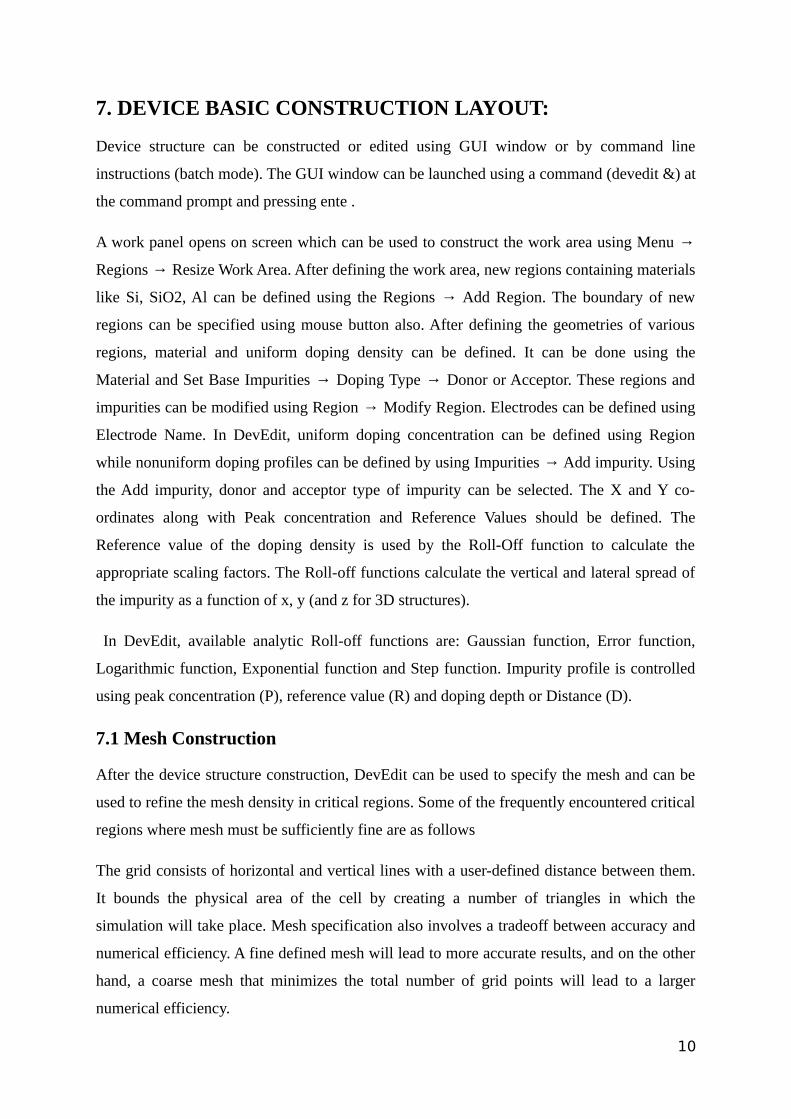
6. DEV-EDIT OVERVIEW
DEVEDIT is a device structure editor. It can be used to generate a new mesh on an existingstructure and can be used to create or modify a device. These devices can then be used by 2D2D and 3D simulators. DEVEDIT can be used as a simulator under DECKBUILD or througha Graphical User Interface (GUI).
Figure 7 DevEdit Base Window Display
9
7. DEVICE BASIC CONSTRUCTION LAYOUT:
Device structure can be constructed or edited using GUI window or by command line
instructions (batch mode). The GUI window can be launched using a command (devedit &) at
the command prompt and pressing ente .
A work panel opens on screen which can be used to construct the work area using Menu →
Regions → Resize Work Area. After defining the work area, new regions containing materials
like Si, SiO2, Al can be defined using the Regions → Add Region. The boundary of new
regions can be specified using mouse button also. After defining the geometries of various
regions, material and uniform doping density can be defined. It can be done using the
Material and Set Base Impurities → Doping Type → Donor or Acceptor. These regions and
impurities can be modified using Region → Modify Region. Electrodes can be defined using
Electrode Name. In DevEdit, uniform doping concentration can be defined using Region
while nonuniform doping profiles can be defined by using Impurities → Add impurity. Using
the Add impurity, donor and acceptor type of impurity can be selected. The X and Y co-
ordinates along with Peak concentration and Reference Values should be defined. The
Reference value of the doping density is used by the Roll-Off function to calculate the
appropriate scaling factors. The Roll-off functions calculate the vertical and lateral spread of
the impurity as a function of x, y (and z for 3D structures).
In DevEdit, available analytic Roll-off functions are: Gaussian function, Error function,
Logarithmic function, Exponential function and Step function. Impurity profile is controlled
using peak concentration (P), reference value (R) and doping depth or Distance (D).
7.1 Mesh Construction
After the device structure construction, DevEdit can be used to specify the mesh and can be
used to refine the mesh density in critical regions. Some of the frequently encountered critical
regions where mesh must be sufficiently fine are as follows
The grid consists of horizontal and vertical lines with a user-defined distance between them.
It bounds the physical area of the cell by creating a number of triangles in which the
simulation will take place. Mesh specification also involves a tradeoff between accuracy and
numerical efficiency. A fine defined mesh will lead to more accurate results, and on the other
hand, a coarse mesh that minimizes the total number of grid points will lead to a larger
numerical efficiency.
10
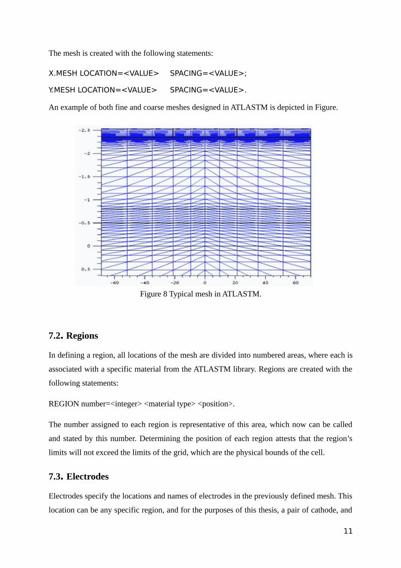
The mesh is created with the following statements:
X.MESH LOCATION=<VALUE> SPACING=<VALUE>;
Y.MESH LOCATION=<VALUE> SPACING=<VALUE>.
An example of both fine and coarse meshes designed in ATLASTM is depicted in Figure.
Figure 8 Typical mesh in ATLASTM.
7.2. Regions
In defining a region, all locations of the mesh are divided into numbered areas, where each is
associated with a specific material from the ATLASTM library. Regions are created with the
following statements:
REGION number=<integer> <material type> <position>.
The number assigned to each region is representative of this area, which now can be called
and stated by this number. Determining the position of each region attests that the region’s
limits will not exceed the limits of the grid, which are the physical bounds of the cell.
7.3. Electrodes
Electrodes specify the locations and names of electrodes in the previously defined mesh. This
location can be any specific region, and for the purposes of this thesis, a pair of cathode, and
11
anode electrodes was assigned in the two individual cells that form the tandem CIGS cell.
The format to define the electrodes is:
ELECTRODE NAME = <electrode name> <position>.
BOTTOM and TOP statements specify that the electrode is positioned along the bottom or
the top of the device, respectively. Otherwise, minimum and maximum position boundaries
must be specified, using the X.MIN, X.MAX, Y.MIN, Y.MAX statements.
7.4. Doping
DOPING specifies doping profiles in the device structure, either analytically or
from an input file. The DOPING statement is:
DOPING <distribution type> <dopant type> <position parameters>.
Uniform, Gaussian or non-standard (user defined from a custom file) distributions can be
used to generate the doping profile. The type and concentration of doping must be defined
next as well as the region to be doped.
7.5. Material
The previously defined and doped region must be associated with specific materials. These
materials, their properties, and physical parameters can be selected from the ATLAS
database, among a number of elements, compounds, and alloys. The user specifies the
material and its properties using the general statement form:
MATERIAL <localization> <material definition>.
A specific example used in this thesis is:
MATERIAL MATERIAL=Si EG300=1.12 PERMITTIVITY=<VALUE> \
AFFINITY=<> MUN=<> MUP=<> NC300=<> NV300=<>.
In this example, the material used is the Si with band gap equal to 1.12 eV,
dielectric permittivity equal to <VALUE> F/m, and electron affinity equal to <VALUE> eV.
More properties include low-field electron and hole mobility, in cm2 /Vs units, equal to ten
and one, respectively. Also, the conduction and valance band densities at 300 respectively.
These material properties and physical parameters are defined for every region consisting of
12
the specific material. The user can change the material properties only in a region by
replacing the second MATERIAL from the above example with a REGION statement
describing this specific region.
7.6. Models
Once we define the mesh, geometry, and doping profiles, we can modify the characteristics of
electrodes, change the default material parameters, and choose which physical models
ATLAS will use during the device simulation. The physical models are grouped into five
classes: mobility, recombination, carrier statistics, impact ionization, and tunneling, and
details for each model are contained in the ATLAS user manual. The general MODELS
statement is:
MODELS <model name>.
Physical models can be enabled on a material-by-material basis. This is useful for
heterojunction device simulation and other simulations where multiple semiconductor regions
are defined and may have different characteristics.
7.7. Solution Method
The numerical methods to be used for solving the equations and parameters associated with
these algorithms are determined by the METHOD statement. Several numerical methods are
contained in the ATLASTM library, but there are three main types.
The GUMMEL method is used for weakly coupled system equations, with only linear
convergence. The NEWTON method is used for strongly coupled system equations, with
quadratic convergence, requiring ATLAS to spend more time solving for quantities which are
essentially constant or weakly coupled. To obtain and ensure convergence, a more accurate
approximation is needed from the system. Finally, the BLOCK method provides faster
simulations when the NEWTON method is unable to provide a reliable solution.
7.8. Solution Specification
ATLAS can calculate DC, AC small signal, and transient solutions. Obtaining solutions is
similar to setting up parametric test equipment for device tests. The user usually defines the
voltages on each electrode in the device. ATLAS then calculates the current through each
13
electrode and the internal quantities, such as carrier concentrations and electric fields
throughout the device.
In all simulations, the device starts with zero bias on all electrodes. Solutions are obtained by
stepping the biases on electrodes from this initial equilibrium condition. To obtain
convergence for the equations used, the user should supply a good initial guess for the
variables to be evaluated at each bias point. The ATLAS solver uses this initial guess and
iterates to a converged solution. Solution specification can be divided up into four parts:
LOG, SOLVE, LOAD, and SAVE.Log files store the terminal characteristics calculated by
ATLAS. These are the currents and voltages for each electrode in DC simulations. For
example, the statement:
LOG OUTF=<FILENAME>
is used to open a log file, and terminal characteristics from all SOLVE statements after the
LOG statement are then saved to this file. Log files contain only the terminal characteristics
and are typically viewed in TONYPLOT.
The SOLVE statement follows a LOG statement and instructs ATLAS to perform a solution
for one or more specified bias points. The LOAD and SAVE statements are used together to
help create better initial guesses for bias points. The SAVE statement saves simulation results
into files for visualization or for future use as an initial guess, and after that the LOAD
statement loads a solution file whenever required to assist in the solution.
7.9. Data Extraction and Plotting
Extracting the data and plotting it is the final section of the input deck. The EXTRACT
statement is provided within the DeckBuild environment. It has a flexible syntax that allows
the user to extract device parameters and construct specific EXTRACT routines. By default,
EXTRACT statements work on the currently open log file, are generally case sensitive, and
operate on the previous solved curve or structure file. All graphics in ATLAS are performed
by saving a file and loading the file into TONYPLOT. The log files produced by ATLAS and
the current-voltage cell characteristic can be plotted and observed in TONYPLOT.
14
8. DEMO EXAMPLE: CREATING A TWO DIMENSIONAL
PAD DIODE STRUCTURE
######################################################################################### GEOMETRY## Width=1um, Thickness=300um## Bulk=n-type, 2e11cm-3########################################################################################
go devedit DevEdit version="2.0" library="1.14"
########################################################################################## Diode Structure########################################################################################
work.area left=0 top=-1 right=1 bottom=301
region reg=1 name=Silicon mat=Silicon color=0xffc000 pattern=0x3 \points="0,0 1,0 1,300 0,300 0,0"
impurity id=1 region.id=1 imp=Phosphorus color=0x906000 \x1=0 x2=1 y1=0 y2=300 \peak.value=2e11 ref.value=0 comb.func=Multiply \rolloff.y=both conc.func.y=Constant \rolloff.x=both conc.func.x=Constant
constr.mesh region=1 default
########################
region reg=2 name=anode mat=Aluminum elec.id=1 work.func=4.1 color=0xffc8c8 pattern=0x6 \
points="0,0 1,0 1,-1 0,-1 0,0"
constr.mesh region=2 default
########################
region reg=3 name=cathode mat=Aluminum elec.id=2 work.func=4.1 color=0xffc8c8 pattern=0x6 \
points="0,300 1,300 1,301 0,301 0,300"
constr.mesh region=3 default
########################
impurity id=2 region.id=1 imp=Boron color=0x906000 \x1=0 x2=1 y1=0 y2=0 \peak.value=1e19 ref.value=2e11 comb.func=Multiply \
15
rolloff.y=both conc.func.y="Gaussian (Dist)" conc.param.y=2.0 \rolloff.x=both conc.func.x="Gaussian (Dist)" conc.param.x=0
impurity id=3 region.id=1 imp=Phosphorus color=0x906000 \x1=0 x2=1 y1=300 y2=300 \peak.value=1e19 ref.value=2e11 comb.func=Multiply \rolloff.y=both conc.func.y="Gaussian (Dist)" conc.param.y=2 \rolloff.x=both conc.func.x="Gaussian (Dist)" conc.param.x=0
############################################################################################ Mesh Formation and Refinement##########################################################################################
base.mesh height=5 width=5bound.cond !apply max.slope=28 max.ratio=300 rnd.unit=0.001 line.straightening=1 align.points when=automatic
imp.refine imp="NetDoping" sensitivity=1.25constr.mesh max.angle=90 max.ratio=300 max.height=1 max.width=0.1 min.height=0.02 min.width=0.02
Mesh Mode=MeshBuildconstr.mesh type=Semiconductor defaultconstr.mesh type=Insulator defaultconstr.mesh type=Metal defaultconstr.mesh type=Other default
refine mode=x x1=0 y1=-1 x2=1 y2=1refine mode=y x1=0 y1=-1 x2=1 y2=1
structure outf=n-type-2e11-diode.str
SIMULATING A PAD DIODE (Non Irradiate)
go atlas mesh infile= n-type-2e11-diode.strmaterial material=silicon region=1 Eg300=1.12 TAUN0=1e-4 TAUP0=1e-4contact name=anode resistance=1e6
model bipolar temp=253.0 print
impact SELB
solve initmethod newton climit=1e-4 maxtrap=25
log outfile= n-type-2e11-fluence-0.logsolve vcathode=0 vstep=10 vfinal=500 name=cathode AC FREQ=1e3 ANAME=anodestructure outf= n-type-2e11-fluence-0-500V.str
SIMULATING A PAD DIODE (Irradiate)
16
go atlas mesh infile= n-type-2e11-diode.strmaterial material=silicon region=1 Eg300=1.12 TAUN0=1e-4 TAUP0=1e-4contact name=anode resistance=1e6
trap e.level=0.51 acceptor density=8e13 degen=1 \sign=2e-14 sigp=2.6e-14trap e.level=0.48 donor density=6e13 degen=1 \sign=2e-14 sigp=2e-14
model bipolar temp=253.0 print
impact SELB
solve initmethod newton climit=1e-4 maxtrap=25
log outfile= n-type-2e11-fluence-2e13.logsolve vcathode=0 vstep=10 vfinal=500 name=cathode AC FREQ=1e3 ANAME=anodestructure outf= n-type-2e11-fluence-2e13-two-trap-500V.str
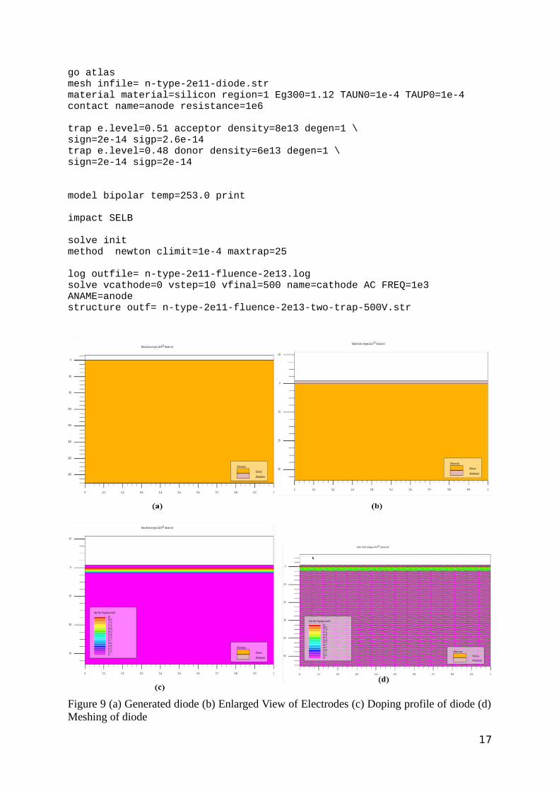
Figure 9 (a) Generated diode (b) Enlarged View of Electrodes (c) Doping profile of diode (d)Meshing of diode
17
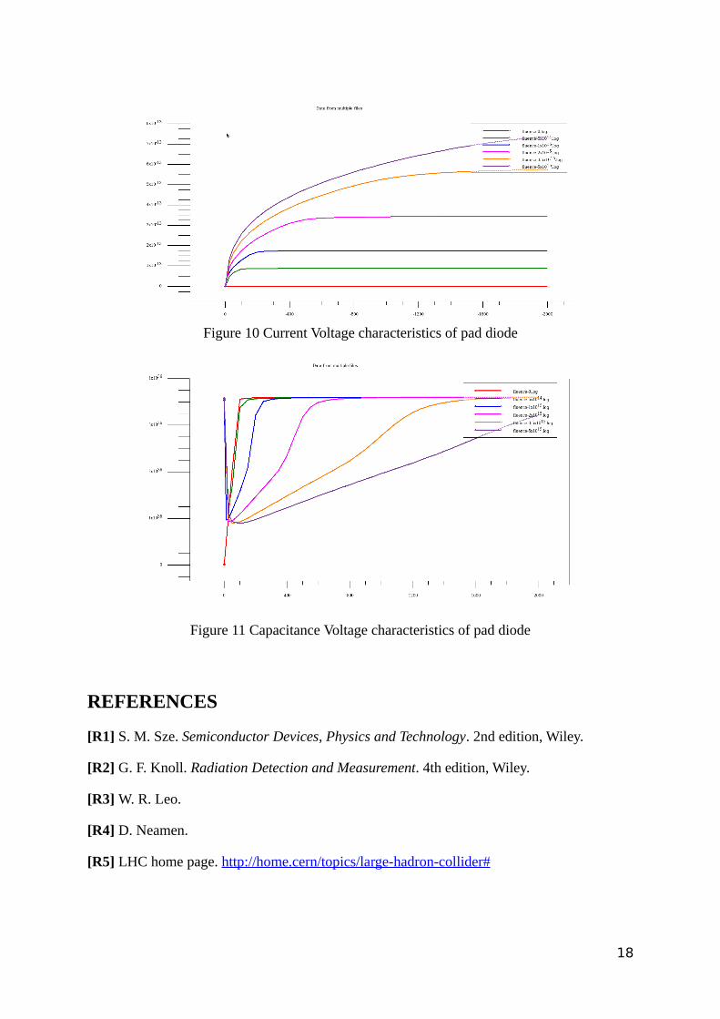
Figure 10 Current Voltage characteristics of pad diode
Figure 11 Capacitance Voltage characteristics of pad diode
REFERENCES
[R1] S. M. Sze. Semiconductor Devices, Physics and Technology. 2nd edition, Wiley.
[R2] G. F. Knoll. Radiation Detection and Measurement. 4th edition, Wiley.
[R3] W. R. Leo.
[R4] D. Neamen.
[R5] LHC home page. http://home.cern/topics/large-hadron-collider#
18