l2432 lcd
TRANSCRIPT

AN No.SIG-CHMO9805A
Liquid Crystal DisplaysLiquid Crystal Displays
Application NotesApplication Notes
Seiko Instruments GmbHSeiko Instruments GmbH
Standard Character ModulesStandard Character Modules

AN No.SIG-CHMO9805A
Notice
This manual describes the technical information, the functions, and the instructions of Liquid CrystalDisplay Modules from Seiko Instruments GmbH. Please read this instruction manual carefully tofamiliarise yourself with the functions and make the best use of them. The descriptions here aresubject to change without notice.
Revision Record
Edition Revision Date
1 Original May 29,1998
Seiko Instruments GmbH 1998
Printed in Germany
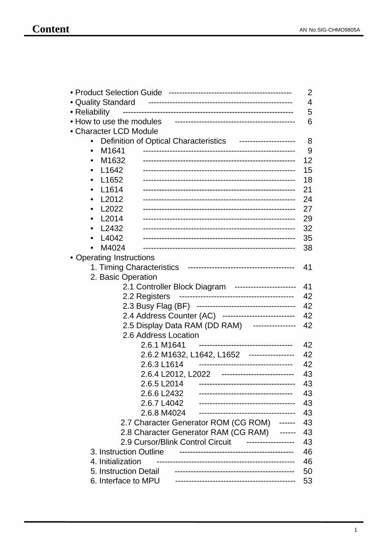
AN No.SIG-CHMO9805AContent
• Product Selection Guide ---------------------------------------------- 2• Quality Standard ------------------------------------------------------ 4• Reliability ---------------------------------------------------------------- 5• How to use the modules --------------------------------------------- 6• Character LCD Module
• Definition of Optical Characteristics --------------------- 8• M1641 --------------------------------------------------------- 9• M1632 --------------------------------------------------------- 12• L1642 --------------------------------------------------------- 15• L1652 --------------------------------------------------------- 18• L1614 --------------------------------------------------------- 21• L2012 --------------------------------------------------------- 24• L2022 --------------------------------------------------------- 27• L2014 --------------------------------------------------------- 29• L2432 --------------------------------------------------------- 32• L4042 --------------------------------------------------------- 35• M4024 --------------------------------------------------------- 38
• Operating Instructions1. Timing Characteristics ---------------------------------------- 412. Basic Operation
2.1 Controller Block Diagram ----------------------- 41 2.2 Registers ------------------------------------------- 42 2.3 Busy Flag (BF) ------------------------------------- 42 2.4 Address Counter (AC) --------------------------- 42 2.5 Display Data RAM (DD RAM) ---------------- 42 2.6 Address Location
2.6.1 M1641 ----------------------------------- 422.6.2 M1632, L1642, L1652 ----------------- 422.6.3 L1614 ----------------------------------- 422.6.4 L2012, L2022 --------------------------- 432.6.5 L2014 ------------------------------------ 432.6.6 L2432 ----------------------------------- 432.6.7 L4042 ------------------------------------ 432.6.8 M4024 ------------------------------------ 43
2.7 Character Generator ROM (CG ROM) ------ 432.8 Character Generator RAM (CG RAM) ------ 432.9 Cursor/Blink Control Circuit ------------------ 43
3. Instruction Outline ------------------------------------------- 464. Initialization ---------------------------------------------------- 465. Instruction Detail --------------------------------------------- 506. Interface to MPU --------------------------------------------- 53
1

AN No.SIG-CHMO9805AProduct Selection Guide
Character Format (character x line) 16 x 1 16 x 2 16 x 2 16 x 2 16 x 4 20 x 2
Model M1641 M1632 L1642 L1652 L1614 L2012
Ref lective M16410AS M16320AS L164200J000S L165200J200S L161400J000S L201200J000S
EL backlight M16419DWS M16329DWS L164221J000S L165221J200S L161421J000S L201221J000S
LED backlight M16417DYS M16327DYS L1642B1J000S L1652B1J200S L1614B1J000S L2012B1J000S
Ref lective (w ide temp) M16410CS M16320CS L164200L000S L165200L200S L161400L000S L201200L000S
LED backlight (w ide temp) M16417JYS M16327JYS L1642B1L000S L1652B1L200S L1614B1L000S L2012B1L000S
Character font 5x7 dots + cursor 5x7 dots + cursor 5x7 dots + cursor 5x7 dots + cursor 5x7 dots + cursor 5x7 dots + cursor
Module Ref lective 80,0 x 36,0 x 11,3 85,0 x 30,0 x 10,1 80,0 x 36,0 x 11,3 122,0 x 44,0 x 11,3 87,0 x 60,0 x 11,6 116,0 x 37,0 x 11,3
size EL backlight 80,0 x 36,0 x 11,3 85,0 x 30,0 x 10,1 80,0 x 36,0 x 11,3 122,0 x 44,0 x 11,3 87,0 x 60,0 x 11,6 116,0 x 37,0 x 11,3
(HxVxT) mm LED backlight 80,0 x 36,0 x 15,8 80,0 x 30,0 x 15,8 80,0 x 36,0 x 15,8 122,0 x 44,0 x 15,8 87,0 x 60,0 x 15,8 116,0 x 37,0 x 15,8
View ing area (HxV) mm 64,5 x 13,8 62,0 x 16,0 64,5 x 13,8 99,0 x 24,0 61,8 x 25,2 83,0 x 18,6
Character size (HxV) mm 3,07 x 5,73 2,78 x 4,27 2,95 x 3,80 4,84 x 8,06 2,95 x 4,15 3,20 x 4,85
Dot size (HxV) mm 0,55 x 0,75 0,50 x 0,55 0,50 x 0,55 0,92 x 1,10 0,55 x 0,55 0,60 x 0,65
Pow er supply voltage (VDD-VSS) + 5 V + 5 V + 5 V + 5 V + 5 V + 5 V
Current consumption IDD 1,5 2,0 1,6 2,0 2,7 2,0
(mA,typ) ILC 0,2 0,2 0,3 0,4 1,1 0,4
Driving method (duty) 1/16 1/16 1/16 1/16 1/16 1/16
KS0066 KS0066 KS0066 KS0066 KS0066 KS0066
Built-in LSI or equivalent MSM5839 MSM5839 MSM5839 KS0063 KS0063
or equivalent or equivalent or equivalent or equivalent or equivalent
Operating normal temp. 0 to + 50 0 to + 50 0 to + 50 0 to + 50 0 to + 50 0 to + 50
temperature ( ºC) w ide temp. - 20 to + 70 - 20 to + 70 - 20 to + 70 - 20 to + 70 - 20 to + 70 - 20 to + 70
Storage normal temp. - 20 to + 60 - 20 to + 60 - 20 to + 60 - 20 to + 60 - 20 to + 60 - 20 to + 60
temperature ( ºC) w ide temp. - 30 to + 80 - 30 to + 80 - 30 to + 80 - 30 to + 80 - 30 to + 80 - 30 to + 80
Weight Ref lective 25 25 25 50 50 40
(g, typ.) EL backlight 30 30 30 55 55 45
LED backlight 35 40 35 65 65 60
Model 5S 5S 5S 5C 5A 5A
Inverters Pow er supply (V) + 5.0 + 5,0 + 5.0 + 5.0 + 5.0 + 5.0
for EL current consumption (mA) 10 10 10 35 45 45
Forw ard current
LED consumption (mA) 100 112 100 240 200 154
backlight Forw ard input voltage
(V,typ.) + 4,1 + 4,1 + 4,1 + 4,1 + 4,1 + 4,1
Page 9 12 15 18 21 24
Dot Matrix Liquid Crystal Display ModuleCharacter Type
• Slim, light-weight and low power consumption• High contrast and wide viewing angle• Built-in controller for easy interface• Available EL and LED backlight type• Available in wide temperature type
FEATURES
2
The table below shows a quick reference guide of the character LCD modules. You can see the standardspecifications and other optical specifications on the reference page of each model shown in the table below.

AN No.SIG-CHMO9805AProduct Selection Guide
Character Format (character x line) 20 x 2 20 x 4 24 x 2 40 x 2 40 x 4
Model L2022 L2014 L2432 L4042 M4024
Reflective - L201400J000S L243200J000S L404200J000S M40240AS
EL backlight - L201421J000S L243221J000S L404221J000S M40249DWS
LED backlight - L2014B1J000S L2432B1J000S L4042B1J000S M40247DYS
Reflective (w ide temp) L202200P000S L201400L000S L243200L000S L404200L000S M40240CS
LED backlight (w ide temp) L2022B1P000S L2014B1L000S L2432B1L000S L4042B1L000S M40247JYS
Character font 5x7 dots + cursor 5x7 dots + cursor 5x7 dots + cursor 5x7 dots + cursor 5x7 dots + cursor
Module Reflective 180,0 x 40,0 x 10,5 98,0 x 60,0 x 11,6 118,0 x 36,0 x 11,3 182,0 x 33,5 x 11,3 190,0 x 54,0 x 10,1
size EL backlight 180,0 x 40,0 x 10,5 98,0 x 60,0 x 11,6 118,0 x 36,0 x 11,3 182,0 x 33,5 x 11,3 190,0 x 54,0 x 10,1
(HxVxT) mm LED backlight 180,0 x 40,0 x 14,8 98,0 x 60,0 x 15,8 118,0 x 36,0 x 15,8 182,0 x 33,5 x 16,3 190,0 x 54,0 x 16,3
View ing area (HxV) mm 149,0 x 23,0 76,0 x 25,2 94,5 x 17,8 154,4 x 15,8 147,0 x 29,5
Character size (HxV) mm 6,00 x 9,66 2,95 x 4,15 3,20 x 4,85 3,20 x 4,85 2,78 x 4,27
Dot size (HxV) mm 1,12 x 1,12 0,55 x 0,55 0,60 x 0,65 0,60 x 0,65 0,50 x 0,55
Pow er supply voltage (VDD-VSS) + 5 V + 5 V + 5 V + 5 V + 5 V
Current consumption IDD 4,2 2,9 2,5 3,0 8,0
(mA,typ) ILC 2,6 1,2 0,5 1,0 3,0
Driving method (duty) 1/16 1/16 1/16 1/16 1/16
KS0066 KS0066 KS0066 KS0066 KS0066
Built-in LSI KS0063 MSM5839 KS0063 KS0063 MSM5839
or equivalent or equivalent or equivalent or equivalent or equivalent
Operating normal temp. - 0 to + 50 0 to + 50 0 to + 50 0 to + 50
temperature ( ºC) w ide temp. - 20 to + 70 - 20 to + 70 - 20 to + 70 - 20 to + 70 - 20 to + 70
Storage normal temp. - - 20 to + 60 - 20 to + 60 - 20 to + 60 - 20 to + 60
temperature ( ºC) w ide temp. - 30 to + 80 - 30 to + 80 - 30 to + 80 - 30 to + 80 - 30 to + 80
Weight Reflective 80 55 40 70 90
(g, typ.) EL backlight - 60 45 75 105
LED backlight 110 70 60 95 140
Model - 5A 5A 5C 5D
Inverters Pow er supply (V) + 5.0 + 5.0 + 5.0 + 5.0 + 5.0
for EL current consumption (mA) - 45 45 25 80
Forw ard current
LED consumption (mA) 320 240 150 260 480
backlight Forw ard input voltage
(V,typ.) + 4,1 + 4,1 + 4,1 + 4,1 + 4,1
Page 27 29 32 35 38
Dot Matrix Liquid Crystal Display ModuleCharacter Type
• Slim, light-weight and low power consumption• High contrast and wide viewing angle• Built-in controller for easy interface• Available EL and LED backlight type• Available in wide temperature type
FEATURES
The table below shows a quick reference guide of the character LCD modules. You can see the standardspecifications and other optical specifications on the reference page of each model shown in the table below.
3

AN No.SIG-CHMO9805AQuality Standard
2. Shipping assurance level is as follows
Rank Zone Defect AQL
Major defect A Display area Display functions
(Appearance) current consumption 0.4%
(Functions) Missing display functions
No display
Minor defect A Display area Polarizer defect
Uneven contrast
Crosstalk
Black spots
B Boundary of display area Black streaks 1.0%
to view ing area Bubbles
Cromaticity
Uniformity
C Panel frame Scratches
Circuit board Dirt
3. Zone definition
A : Active display area
B : Viewing area
C : Outside of window
A : active display areaB : viewing area excluding active display areaC : area of entire module excluding viewing area (metal frame, PCB etc)
1. Quality Assurance 1.1 Conformity
The performances, functions, and reliability of the products conform to the Product Specification. 1.2 Responsibility
Customers are responsible for any defect in quality caused after incoming inspection. 1.3 Warranty
The quality warranty is valid for one year after the delivery.
4. Appearance Defect See individual defects standards in Delivery Specifications
4

AN No.SIG-CHMO9805AReliability
Test Item Test Conditions result
Operation at 40 ºC ± 2 ºC No abnormalities
high temperature 90% RH for 500 hours in functions* and
and humidity appearance**
Operation at 60 ºC ± 2 ºC for 500hrs No abnormalities
high temperature in functions* and
appearance**
Heat shock -20 ºC ⇔ +60 ºC
Left for 1 hour at No abnormalities
each temperature, in functions* and
transition time 5 minutes appearance**
repeated 10 times
Low Temperature -20 ºC ± 2 ºC for 500hrs No abnormalities
in functions* and
appearance**
Vibration Sweep for 1 min. at
10Hz, 55Hz, 10Hz No abnormalities
amplitude 1.5mm 2 hours in functions* and
each in the X,Y and Z appearance**
directions
Drop shock Dropped onto a board No abnormalities
from a height of 30cm in functions* and
appearance**
* Dissipation current, contrast and display functions
** Ploarizer deterioration, other appearance defect
Test Item Test Conditions result
Operation at 60 ºC ± 2 ºC No abnormalities
high temperature 90% RH for 500 hours in functions* and
and humidity appearance**
Operation at 80 ºC ± 2 ºC for 500hrs No abnormalities
high temperature in functions* and
appearance**
Heat shock -30 ºC ⇔ +80 ºC
Left for 1 hour at No abnormalities
each temperature, in functions* and
transition time 5 minutes appearance**
repeated 10 times
Low Temperature -30 ºC ± 2 ºC for 500hrs No abnormalities
in functions* and
appearance**
Vibration Sw eep for 1 min. at
10Hz, 55Hz, 10Hz No abnormalities
amplitude 1.5mm 2 hours in functions* and
each in the X,Y and Z appearance**
directions
Drop shock Dropped onto a board No abnormalities
from a height of 30cm in functions* and
appearance**
* Dissipation current, contrast and display functions
** Polarizer deterioration, other appearance defect
1. Reliability Test1.1 Normal Temperature type
1.2 Wide Temperature type
Item Conditions Standard Unit
Life time 25 ºC ± 10 ºC 100,000 or more hours
< 65 %RH
2. LCD Life Time
3. Definition of LCD service life• Contrast becomes 30% of initial value• Current consumption becomes three times higher than
initial value• Remarkable alignment deterioration occurs in LCD
cell layer• Unusual operation occurs in display functions
5

AN No.SIG-CHMO9805AHow To Use LCD Module
1. Safety• If the LCD panel is damaged, be careful not to get the liquid
crystal in your mouth and not to be injured by crushedglass.
• If you should swallow the liquid crystal , first wash yourmouth thoroughly with water, then drink a lot of waterinduce vomiting and then consult a physician.
• If the liquid crystal should get in your eyes, flush your eyeswith running water for at least fifteen minutes.
• If the liquid crystal touches your skin or clothes, remove itand wash the affected part of your skin or clothes with soapand running water.
• High voltage is applied to the lead terminals of the EL lamp.Do not touch any part of the lead terminals. (For LCDmodule with EL backlight)
• Do not use EL inverters without a load or in the short-circuitmode.
• Use the LCD module within the rated voltage to preventoverheating and/or damage. Also, take steps to ensure thatthe connector does not come off.
2. LCD Handling• Please keep the temperature within the specified range for
use and storage. Polarization degradation, bubblegeneration or polarizer peel-off may occur with hightemperature and high humidity.
• Do not touch, push or rub the exposed polarizers withanything harder than hardness of 3B (glass, tweezers,etc..).
• When the display surface becomes dusty, wipe gently withabsorbent cotton or other soft material like chamois soakedin petroleum benzene. Do not scrub hard to avoid damagingthe display surface.
• Wipe off saliva or water drops immediately. Contact withwater over a long period of time may cause deformation orcolor fading.
• Avoid contact with oil and fats.• Condensation on the surface and contact terminals due to
cold will damage, stain or dirty the polarizers. After productsare tested at low temperatures they must be warmed up in acontainer before coming in contact with room temperatureair.
• Do not put or attach anything on the display area to avoidleaving marks on.
• Do not touch the display area with bare hands, damage thedisplay area and degrade insulation between terminals.(some cosmetics are detrimental to the polarizers)
• As glass is fragile, it tends to become cracked or chippedduring handling especially on the edges, Please avoiddropping or jarring.
3. LCD Module3.1 Mounting LCD module• Use the specified mounting parts and holes to mount the
module.• Connect a 10 µF capacitor between the power supply
terminals to eliminate noise.
Module
Screw
Transparent plateFitting plate
Small gap
• Make sure that no stress is applied on the module when it ismounted. The application of stress for a long time maydamage the LCD panel and the ICs substrates.
• To protect the polarizer and the LCD panel, cover the displaysurface with a transparent plate, for example, acrylic or glass,with a small gap between the transparent plate and the LCDsurface.
• Do not apply input signals when power supply voltage isn'tapplied.
3.2 Precaution for handling LCD module Since the module has been assembled and adjusted with a
high degree of precision, avoid applying excessive shocks tothe module or making any modifications to it.
• Do not alter, modify or change the shape of the tab on themetal frame.
• Do not make extra holes on the PCB, modify its shape orchange the positions of components attached.
• Do not damage or modify the pattern wiring on the PCB• Do not modify the zebra rubber or touch it with another
materials.• Do not make any modifications with a soldering iron except
indicating area.• Do not drop, bend or twist the module.
3.3 Electro-static discharge Since CMOS ICs are mounted on the module, special
attention has to be paid to the electric-static discharge.• Make sure that you are connected to the ground during
handling of the module.• Before removing the module from packing unit make sure
that the module and yourself have the same electricpotential.
• When soldering the terminal of the module, make sure thatthe AC power source for the soldering iron does not leak.
• When using an electric screwdriver to attach the module, thescrewdriver should be grounded to minimise as much aspossible any transmission of electro-magnetic wavesproduced by sparks coming from the accumulator of themotor.
• Make your clothes and working bench the ground potentialas much as possible.
• Avoid to generate static electricity, relative humidity shouldbe 50 ~ 60 %RH.
3.4 Precaution for operation• Proper operating voltage for LCD gives optimum viewing
angle.• If LCD surface is pressed harder during operation, the
display becomes abnormal and then will return to normalafter the pressure is released. However, it may generatebubbles and cause permanent damage to the LCD.
• Condensation may generate electrochemical reaction andthen it may cause open or short circuit on the terminal.
3.5 Cleaning• Do not wipe the polarizer with a dry cloth, as it may scratch
the surface.• Wipe the module gently with a soft cloth soaked with a
petroleum benzene.• Do not use ketonic solvents (ketone, acetone etc.) or
aromatic solvents (toluene and xylenen) as they maydamage the polarizing plate.
4. Storage• Store the module in the dark place. Keep the temperature
between 15 ºC and 35 ºC and the humidity below 65%RH.• Do not store the module near organic solvents or corrosive
gases.• Make sure that no stress or vibration is applied to the
module when it is stored.• Use the products with EL backlight within 6 months after
receiving them.
6

AN No.SIG-CHMO9805AHow To Use LCD Module
5. Handling the LED backlight• When soldering the LED connector, the soldering iron
temperature should not exceed 260 ºC and soldering timeshould be within 3 seconds
• For cleaning, wipe with soft cloth and use only the followingchemicals Ethanol Isopropyl alcohol
6. Handling the EL backlight• Your design should make it easy to replace the EL backlight
since they have a shorter service life than the othercomponents of LCD modules.
• Do not bend the EL leads when soldering them on the circuitboard of the LCD modules otherwise they may break.
• To set the EL backlight into the LCD module, push the ELbacklight with its emitting side up, without pushing the rubberconnectors too hard. If you damage them, the LCD modulemay not work properly.
• Do not damage the film surface of the EL backlight otherwisethe backlight will be damaged by humidity.
• Since high voltage is applied to the EL lead terminals, becareful not to touch the EL terminals.
• Do not use EL inverters without a load or in the short-circuitmode.
7

AN No.SIG-CHMO9805ACharacter LCD Module
Angles ∅ ∅ and θ θ
θ1θ2(θ=0)
Z
XX’
Y’(∅=180 ° )
Y (∅=180 ° ) (θ=90°)
∅
Viewing Angle θθ11 and θ θ22
2.0
θ2
C max.
θ1
Contrast C
Viewing Angle
C=Brightness (reflection) of non-selected segment (B2)
Brightness (reflection) of selected segment (B1)
B2
B1
Brightness (reflection)of selected segment
Brightness (reflection)of non-selected segment
0
(Dark)
Brightness(reflection)
(bright)
(%)
Operating Voltage (V)
Contrast C
1/fFRM
Vop
r
Unselected state
Selected state(display ON)
Unselected state(display OFF)
100%90%
ton toff
10%
Brightness(transmissin)
(Bright)
(Dark)
Voltage
(V)
Vopr : Operating VoltagefFRM : Frame Frequencyton : Response time (rise)toff : Response time (fall)
Definition of Optical Characteristics Term
Response Time
8

AN No.SIG-CHMO9805A
16 Characters x 1 line5 x 7 Dot Matrix + Cursor1/16 Duty5V single Power SupplyAvailable in EL and LED Backlight type
M1641 (16 x 1)
Note : Only dimension changes between Reflective/EL and LED backlight is the thickness
Absolute Maximum Ratings
Electrical Characteristics
Mechanical Characteristics
Pin Function
Dimensions
VSS=0V, Ta=25ºC
Item Symbol Conditions Min. Max. Unit
Pow er supply VDD -0.3 6.0 V
voltage VLC -0.3 VDD V
Input voltage Vin -0.3 VDD +0.3 V
Operating temperature
Normal Topr 0 +50 ºC
Wide Topr -20 +70 ºC
Storage temperature
Normal Tstg -20 +60 ºC
Wide Tstg -30 +80 ºC
Storage < 48 hrs +20 +85 %RH
humidity <1000 hrs +20 +65 %RH
No. Name Function
1 VSS GND
2 VDD Pow er supply voltage +5V
3 VLC Liquid crystal driving voltage
4 RS L : Instruction code input
H: Data input
5 R/W L : Data w rite from MPU to LCM
H : Data read from LCM to MPU
6 E Enable
7 DB0 Data bus line
8 DB1 Data bus line
9 DB2 Data bus line
10 DB3 Data bus line
11 DB4 Data bus line
12 DB5 Data bus line
13 DB6 Data bus line
14 DB7 Data bus line
Item Specifications Unit
Module size (H x V) 80.0 x 36.0 mm
Thickness Reflective/EL 11.3 mm
LED 15.8 mm
View ing area (H x V) 64.5 x 13.8 mm
Character size w ith cursor (H x V) 3.07 x 6.56 mm
Mounting hole distance (H x V) 75.0 x 31.0 mm
Reflective 25 g
Weight EL backlight 30 g
LED backlight 35 g
H : Horizontal, V : Vertical
VDD=5V± 5%, VSS=0V, Ta=0 ~ 50ºC
Item Symbol Conditions Min. Typ. Max. Unit
Pow er supply VDD 4.75 5.00 5.25 V
voltage VDD - VLC 3.0 - 6.3 V
Input High V IH1 2.2 - VDD V
voltage Low V IL1 0 - 0.6 V
Output High VOH1 -IOH=0.205mA 2.4 - - V
voltage Low VLH1 -IOL=1.2mA - - 0.4 V
Current consumption *
Normal Temp IDD Ta=25ºC - 1.3 2.0 mA
type ILC VLC=0.25V - 0.2 0.6 mA
Wide Temp. IDD Ta=25ºC - 1.6 2.5 mA
type ILC VLC=-0.6V - 0.3 1.0 mA
* test pattern : check board pattern
M1641 (1x16) Unit: mm. General tolerance ±0,5 mm
LED Backlight
9
Reflective/EL Backlight

AN No.SIG-CHMO9805AM1641 (16 x 1)
Optical Characteristics
2.Wide Temperature Range Type
1. Normal Temperature Range Type
1. Absolute Maximum Ratings
2. Electrical Characteristics
LED Backlight
temperature (ºC)
240
60
+25 +70
LED forwardcurrentconsumption(mA)
-200
Anode
Cathode
total number of LED chips =2 x 8 = 16 pcs
* LED forward current consumption and operating temperature characteristics are as follows.
Ta=21ºC, Vopr=4.75V
Item Symbol Conditions Min. Typ. Max. Unit
View ing θ 1 C ≥ 2 - - -15
angle θ 2 Φ = 0 º 55 - - deg.
θ 2 - θ 1 70 - -
Contrast C θ =+2 5 º, Φ = 0 º - 5 - -
ton (rise) θ =0 º - 150 200 msec
Response toff (fall) Φ =0 º - 200 220 msec
time ton (rise) θ = 0 º, Φ = 0 º - 750 800 msec
toff (fall) Ta = 0ºC, Vopr=5.0V - 600 700 msec
Measuring equipment : Canon illuminater LC-4SR
Ta=25ºC
Item Symbol Specifications Unit
LED forw ard current IF 240 mA
consumption *
LED reverse voltage VR 8 V
Allow able loss PD 1.05 W
Operating temperature Topr -20 ~ +70 ºC
Storage Temperature Tstg -40 ~ +80 ºC
Ta=25ºC
Item Symbol Conditions Min. Typ. Max. Unit
LED forw ard VF IF=120mA 3.8 4.1 4.4 V
input voltage
LED reverse IR VR=8V - - 0.16 mA
current
Peak Emitting w avelength IF=120mA* - 570 - nm
Spectral half-w idth IF=120mA* - 30 - nm
Brightness L IF=120mA* 120 150 - cd/m²
Ta=21ºC, 1/16 Duty, Vopr=VDD - VLC
Item Symbol Conditions Min. Typ. Max. Unit
View ing θ 1 C ≥ 2 - - -15
angle θ 2 Φ = 0 º 55 - - deg.
θ 2 - θ 1 70 - -
Contrast C θ =+20 º, Φ = 0 º - 5 - -
Vop=5,6v
ton (rise) θ = 0 º, Φ = 0 º - 150 200 msec
Response toff (fall) Ta = 21ºC, Vopr=5.6V - 200 220 msec
time ton (rise) θ = 0 º, Φ = 0 º - 750 800 msec
toff (fall) Ta = 0ºC, Vopr=5.9V - 600 700 msec
Measuring equipment : Canon illuminater LC-4SR
Circuit Block diagram
Recommended Operating VoltageThe recommended value (Vopr) for an ambient temperature
is as follow s. Vopr=VDD - VLC
Temperature (ºC) -20 0 +25 +50 +70
Vopr (V) Normal - 5.00 4.75 4.50 -
Wide 6.20 5.90 5.60 5.40 5.20
Common Signal
40
Segment Signal
Controller
VDDVSSVLC
DB0 ~ 7
RSR/W
E
LCD (16 x 1)
40
8 8
10

AN No.SIG-CHMO9805AM1641 (16 x 1)
1.Absolute Maximum Ratings
2. Brightness, Current, Life Characteristics
3.4 Inverter Dimensions (unit : mm)
Pin No. Function
1 Input : 5V DC
2 Common : GND
3 Output
EL Backlight
3.1 Electrical Characteristics (When combined with EL lamp)
3.2 Tolerance (Inverter only)
3.3 Maximum Ratings (Inverter only)
3. Suitable Inverter 5S
Item Symbol Standard Unit
Operating Vopr AC 150V, 1KHz V
voltage Sinew ave
Operating Topr 0 ~ +50 ºC
temperature
Storage Tstg -20 ~ + 60 ºC
temperature
Storage 0 ~ 10 % RH (60 ºC)
humidity 0 ~ 30 % RH (40 ºC)
Item Conditions Specifications Unit
Brightness 100V, 400Hz 40 min. cd/m²
Sinew ave
Current 100V, 400Hz 1.5 max. mA
Sinew ave
Life 100V, 400Hz, Sinew ave 3,000
25ºC,50%RH hrs
Using 5S Inverter 6,000
25ºC,50%RH
Ta=25ºC
Item Symbol Conditions Specifications Unit
Oscillating f INV V IN=5VDC 550 typ. Hz
frequency
Output voltage VOUT V IN=5VDC 100 typ. V
Output current IOUT V IN=5VDC 1.5 typ. mA
Input current V IN 10 Vrms
Voltage IIN V IN=5VDC 5 typ VDC
Item Specifications Unit
Input voltage 3.0 to 6.0 V
Load range 25 to 40 cm²
Item Specifications Unit
Input voltage 7.0 V
Load range 50 cm²
Operating temperature -10 to +60 ºC
Storage temperature -20 to +70 ºC
3-∅0.6
15
1.5
5 13
1
23
13
8.5
2.25
2 m
in.
11

AN No.SIG-CHMO9805A
16 Characters x 2 line5 x 7 Dot Matrix + Cursor1/16 Duty5V single Power SupplyAvailable in EL and LED Backlight type
M1632 (16 x 2)
Note : Only dimension changes between Reflective/EL and LED backlight is the thickness.
Absolute Maximum Ratings
Electrical Characteristics
Mechanical Characteristics
Pin Function
Dimensions
VSS=0V, Ta=25ºC
Item Symbol Conditions Min. Max. Unit
Pow er supply VDD -0.3 6.0 V
voltage VLC -0.3 VDD V
Input voltage Vin -0.3 VDD +0.3 V
Operating temperature
Normal Topr 0 +50 ºC
Wide Topr -20 +70 ºC
Storage temperature
Normal Tstg -20 +60 ºC
Wide Tstg -30 +80 ºC
Storage < 48 hrs +20 +85 %RH
humidity <1000 hrs +20 +65 %RH
No. Name Function
1 VSS GND
2 VDD Pow er supply voltage +5V
3 VLC Liquid crystal driving voltage
4 RS L : Instruction code input
H: Data input
5 R/W L : Data w ri te from MPU to LCM
H : Data read from LCM to MPU
6 E Enable
7 DB0 Data bus line
8 DB1 Data bus line
9 DB2 Data bus line
10 DB3 Data bus line
11 DB4 Data bus line
12 DB5 Data bus line
13 DB6 Data bus line
14 DB7 Data bus line
( 15 ) A Anode (+) for LED backlight( 16 ) K Cathode (-) for LED backlight
Item Specifications Unit
Module size (H x V) 85.0 x 30.0 mm
Thickness Reflective/EL 10.1 mm
LED 15.8 mm
View ing area (H x V) 62.0 x 16.0 mm
Character size w ith cursor (H x V) 2.78 x 4.89 mm
Mounting hole distance (H x V) 82.0 x 24.0 mm
Reflective 25 g
Weight EL backlight 30 g
LED backlight 40 g
H : Horizontal, V : Vertical
VDD=5V± 5%, VSS=0V, Ta=0 ~ 50ºC
Item Symbol Conditions Min. Typ. Max. Unit
Pow er supply VDD 4.75 5.00 5.25 V
voltage VDD - VLC 3.0 - 6.3 V
Input High V IH1 2.2 - VDD V
voltage Low V IL1 0 - 0.6 V
Output High VOH1 -IOH=0.205mA 2.4 - - V
voltage Low VLH1 -IOL=1.2mA - - 0.4 V
Current consumption *
Normal Temp IDD Ta=25ºC - 1.6 2.5 mA
type ILC VLC=0.25V - 0.2 1.0 mA
Wide Temp. IDD Ta=25ºC - 1.6 2.5 mA
type ILC VLC=-0.6V - 0.3 1.0 mA
* test pattern : check board pattern
M1632 (2x16) Unit: mm, General tolerance ±0.5 mm
LED BacklightReflective/EL Backlight
12

AN No.SIG-CHMO9805AM1632 (16 x 2)
Optical Characteristics
2.Wide Temperature Range Type
1. Normal Temperature Range Type
1. Absolute Maximum Ratings
2. Electrical Characteristics
LED Backlight
temperature (ºC)
200
116
+25 +70
LED forwardcurrentconsumption(mA)
-200
Anode
Cathode
total number of LED chips =2 x 8 = 16 pcs
* LED forward current consumption and operating temperature characteristics are as follows.
Ta=21ºC, 1/16 Duty, Vopr=4.75V
Item Symbol Conditions Min. Typ. Max. Unit
View ing θ 1 C ≥ 2 - - -15
angle θ 2 Φ = 0 º 55 - - deg.
θ 2 - θ 1 70 - -
Contrast C θ =+2 5 º, Φ = 0 º - 5 - -
ton (rise) θ =0 º - 150 200 msec
Response toff (fall) Φ =0 º - 200 220 msec
time ton (rise) θ = 0 º, Φ = 0 º - 750 800 msec
toff (fall) Ta = 0ºC, Vopr=5.0V - 600 700 msec
Measuring equipment : Canon illuminater LC-4SR
Ta=25ºC
Item Symbol Specifications Unit
LED forw ard current IF 200 mA
consumption *
LED reverse voltage VR 8 V
Allow able loss PD 0.92 W
Operating Temperature Topr - 20 ~ +70 ºC
Storage Temperature Tstg - 40 ~ + 80 ºC
Ta=25ºC
Item Symbol Conditions Min. Typ. Max. Unit
LED forw ard VF IF=112mA 3.8 4.1 4.4 V
input voltage
LED reverse IR VR=8V - - 0.16 mA
current
Brightness L IF=112mA* 40 50 - cd/m²
Ta=21ºC, 1/16 Duty, Vopr=VDD - VLC
Item Symbol Conditions Min. Typ. Max. Unit
View ing θ 1 C ≥ 2 - - -15
angle θ 2 Φ = 0 º 55 - - deg.
θ 2 - θ 1 Vop=5,6v 70 - -
Contrast C θ =+20 º, Φ = 0 º - 5 - -
Vop=5,6v
ton (rise) θ = 0 º, Φ = 0 º - 150 200 msec
Response toff (fall) Ta = 21ºC, Vopr=5.6V - 200 220 msec
time ton (rise) θ = 0 º, Φ = 0 º - 750 800 msec
toff (fall) Ta = 0ºC, Vopr=5.9V - 600 700 msec
Measuring equipment : Canon illuminater LC-4SR
Circuit Block diagram
Recommended Operating VoltageThe recommended value (Vopr) for an ambient temperature
is as follow s. Vopr=VDD - VLC
Temperature (ºC) -20 0 +25 +50 +70
Vopr (V) Normal - 5.00 4.75 4.50 -
Wide 6.20 5.90 5.60 5.40 5.20
Timing Signal 3
Common Signal
Serial Data
Segment Signal
16
40Controller
VDDVSSVLC
DB0 ~ 7
RSR/W
E
LCD (16 x 2)
40
SegmentDriver
13

AN No.SIG-CHMO9805AM1632 (16 x 2)
1.Absolute Maximum Ratings
2. Brightness, Current, Life Characteristics
3.4 Inverter Dimensions (unit : mm)
Pin No. Function
1 Input : 5V DC
2 Common : GND
3 Output
EL Backlight
3.1 Electrical Characteristics (When combined with EL lamp)
3.2 Tolerance (Inverter only)
3.3 Maximum Ratings (Inverter only)
3. Suitable Inverter 5S
Item Symbol Standard Unit
Operating Vopr AC 150V, 1KHz V
voltage Sinew ave
Operating Topr -10 ~ +50 ºC
temperature
Storage Tstg -20 ~ + 60 ºC
temperature
Storage 0 ~ 10 % RH (60 ºC)
humidity 0 ~ 30 % RH (40 ºC)
Item Conditions Specifications Unit
Brightness 100V, 400Hz 30 min. cd/m²
Sinew ave 35 typ.
Current 100V, 400Hz 1.2 typ. mA
Sinew ave 1.7 max
Life * 100V, 400Hz, Sinew ave 1,500
25ºC,50%RH hrs
Using 5S Inverter 4,000
25ºC,50%RH
* Def inition of Life : Used continuously dow n to 10 cd/m²
Ta=25ºC
Item Symbol Conditions Specifications Unit
Oscillating f INV V IN=5VDC 550 typ. Hz
frequency
Output voltage VOUT V IN=5VDC 100 typ. V
Output current IOUT V IN=5VDC 1.5 typ. mA
Input current V IN 5 typ VDC
voltage IIN V IN=5VDC 10 typ mA
Initial brightness B V IN=5VDC 35 typ. cd/m²
Surface brightness BP V IN=5VDC 7 typ. cd/m²
(panel upper side) Vopr=0V
Item Specifications Unit
Input voltage 3.0 to 6.0 V
Load range 5 to 15 cm²
Item Specifications Unit
Input voltage 7.0 V
Load range 50 cm²
Operating temperature -10 to +60 ºC
Storage temperature -20 to +70 ºC
3-∅ 0.6
15
1.5
5 13
1
23
13
8.5
2.25
2 m
in.
14

AN No.SIG-CHMO9805A
16 Characters x 2 line5 x 7 Dot Matrix + Cursor1/16 Duty5V single Power SupplyAvailable in EL and LED Backlight type
L1642 (16 x 2)
Note : Only dimension changes between Reflective/EL and LED backlight is thickness.
Absolute Maximum Ratings
Electrical Characteristics
Mechanical Characteristics
Pin Function
Dimensions
VSS=0V, Ta=25ºC
Item Symbol Conditions Min. Max. Unit
Pow er supply VDD -0.3 6.0 V
voltage VLC -0.3 VDD V
Input voltage Vin -0.3 VDD +0.3 V
Operating temperature
Normal Topr 0 +50 ºC
Wide Topr -20 +70 ºC
Storage temperature
Normal Tstg -20 +60 ºC
Wide Tstg -30 +80 ºC
Storage < 48 hrs +20 +85 %RH
humidity <1000 hrs +20 +65 %RH
No. Name Function
1 VSS GND
2 VDD Pow er supply voltage +5V
3 VLC Liquid crystal driving voltage
4 RS L : Instruction code input
H: Data input
5 R/W L : Data w rite from MPU to LCM
H : Data read from LCM to MPU
6 E Enable
7 DB0 Data bus line
8 DB1 Data bus line
9 DB2 Data bus line
10 DB3 Data bus line
11 DB4 Data bus line
12 DB5 Data bus line
13 DB6 Data bus line
14 DB7 Data bus line
( 15 ) A Anode (+) for LED backlight
( 16 ) K Cathode (-) for LED backlight
Item Specifications Unit
Module size (H x V) 80.0 x 36.0 mm
Thickness Reflective/EL 11.3 mm
LED 15.8 mm
View ing area (H x V) 64.5 x 13.8 mm
Character size w ith cursor (H x V) 2.95 x 4.35 mm
Mounting hole distance (H x V) 75.0 x 31.0 mm
Reflective 25 g
Weight EL backlight 30 g
LED backlight 35 g
H : Horizontal, V : Vertical
VDD=5V± 5%, VSS=0V, Ta=0 ~ 50ºC
Item Symbol Conditions Min. Typ. Max. Unit
Pow er supply VDD 4.75 5.00 5.25 V
voltage VDD - VLC 3.0 - 6.3 V
Input High V IH1 2.2 - VDD V
voltage Low V IL1 0 - 0.6 V
Output High VOH1 -IOH=0.205mA 2.4 - - V
voltage Low VLH1 -IOL=1.2mA - - 0.4 V
Current consumption *
Normal Temp IDD Ta=25ºC - 1.6 3.0 mA
type ILC VLC=0.25V - 0.3 1.0 mA
Wide Temp. IDD Ta=25ºC - 1.6 3.0 mA
type ILC VLC=-0.6V - 0.4 1.0 mA
* test pattern : check board pattern
L1642 (2x16) Unit: mm, General tolerance ±0.5 mm
LED BacklightReflective/EL Backlight
15

AN No.SIG-CHMO9805AL1642 (16 x 2)
Optical Characteristics
2.Wide Temperature Range Type
1. Normal Temperature Range Type
1. Absolute Maximum Ratings
2. Electrical Characteristics
LED Backlight
240
60
+25 +70
LED forwardcurrentconsumption(mA)
temperature (ºC)-20
0
Anode
Cathode
total number of LED chips =2 x 12 = 24 pcs
* LED forward current consumption and operating temperature characteristics are as follows.
Ta=21ºC, 1/16 Duty, Vopr=4.75V
Item Symbol Conditions Min. Typ. Max. Unit
View ing θ 1 C ≥ 2 - - -15
angle θ 2 Φ = 0 º 55 - - deg.
θ 2 - θ 1 70 - -
Contrast C θ =+2 5 º, Φ = 0 º - 5 - -
ton (rise) θ =0 º - 150 200 msec
Response toff (fall) Φ =0 º - 200 220 msec
time ton (rise) θ = 0 º, Φ = 0 º - 750 800 msec
toff (fall) Ta = 0ºC, Vopr=5.0V - 600 700 msec
Measuring equipment : Canon illuminater LC-4SR
Ta=25ºC
Item Symbol Specifications Unit
LED forw ard current IF 240 mA
consumption *
LED reverse voltage VR 8 V
Allow able loss PD 1.05 W
Operating Temperature Topr - 20 ~ +70 ºC
Storage Temperature Tstg - 40 ~ + 80 ºC
Ta=25ºC
Item Symbol Conditions Min. Typ. Max. Unit
LED forw ard VF IF=120mA 3.8 4.1 4.4 V
input voltage
LED reverse IR VR=8V - - 0.2 mA
current
Peak emitting IR IF=120mA* - 570 - nm
w avelength
Spectral DI IF=120mA* - 30 - nm
half-w idth
Brightness L IF=120mA* - 40 50 cd/m²
Ta=21ºC, 1/16 Duty, Vopr=VDD - VLC
Item Symbol Conditions Min. Typ. Max. Unit
View ing θ 1 C ≥ 2 - - -15
angle θ 2 Φ = 0 º 55 - - deg.
θ 2 - θ 1 Vop=5,6v 70 - -
Contrast C θ =+20 º, Φ = 0 º - 5 - -
Vop=5,6v
ton (rise) θ = 0 º, Φ = 0 º - 150 200 msec
Response toff (fall) Ta = 21ºC, Vopr=5.6V - 200 220 msec
time ton (rise) θ = 0 º, Φ = 0 º - 750 800 msec
toff (fall) Ta = 0ºC, Vopr=5.9V - 600 700 msec
Measuring equipment : Canon illuminater LC-4SR
Circuit Block diagram
Recommended Operating VoltageThe recommended value (Vopr) for an ambient temperature
is as follow s. Vopr=VDD - VLC
Temperature (ºC) -20 0 +25 +50 +70
Vopr (V) Normal - 5.00 4.75 4.50 -
Wide 6.20 5.90 5.60 5.40 5.20
Common Signal
Timing Signal3
Serial Data
Segment Signal
16
40Controller
VDDVSSVLC
DB0 ~ 7
RSR/W
E
LCD (16 x 2)
40
SegmentDriver
16

AN No.SIG-CHMO9805AL1642 (16 x 2)
1.Absolute Maximum Ratings
2. Brightness, Current, Life Characteristics
3.4 Inverter Dimensions (unit : mm)
Pin No. Function
1 Input : 5V DC
2 Common : GND
3 Output
EL Backlight
3.1 Electrical Characteristics (When combined with EL lamp)
3.2 Tolerance (Inverter only)
3.3 Maximum Ratings (Inverter only)
3. Suitable Inverter 5S
Item Symbol Standard Unit
Operating Vopr AC 150V, 1KHz V
voltage Sinew ave
Operating Topr 0 ~ +50 ºC
temperature
Storage Tstg -20 ~ + 60 ºC
temperature
Storage 0 ~ 10 % RH (60 ºC)
humidity 0 ~ 30 % RH (40 ºC)
Item Conditions Specifications Unit
Brightness 100V, 400Hz 30 min. cd/m²
Sinew ave 35 typ.
Current 100V, 400Hz 1.2 typ. mA
Sinew ave 1.7 max
Life 100V, 400Hz, Sinew ave 1,500
25ºC,50%RH hrs
Using 5S Inverter 4,000
25ºC,50%RH
Item Specifications Unit
Input voltage 3.0 to 6.0 V
Load range 25 to 40 cm²
Item Specifications Unit
Input voltage 7.0 V
Load range 50 cm²
Operating temperature -10 to +60 ºC
Storage temperature -20 to +70 ºC
3-∅0.6
15
1.5
5 13
1
23
13
8.5
2.25
2 m
in.
Ta=25ºC
Item Symbol Conditions Specifications Unit
Oscillating f INV V IN=5VDC 550 typ. Hz
frequency
Output voltage VOUT V IN=5VDC 100 typ. V
Output current IOUT V IN=5VDC 1.5 typ. mA
Input current V IN 10 Vrms
voltage IIN V IN=5VDC 5 typ VDC
17

AN No.SIG-CHMO9805A
16 Characters x 2 line5 x 7 Dot Matrix + Cursor1/16 Duty5V single Power SupplyAvailable in EL and LED Backlight type
L1652 (16 x 2)
Note : Only dimension changes between Reflective/EL and LED backlight is thickness.
Absolute Maximum Ratings
Electrical Characteristics
Mechanical Characteristics
Pin Function
Dimensions
VSS=0V, Ta=25ºC
Item Symbol Conditions Min. Max. Unit
Pow er supply VDD -0.3 6.0 V
voltage VLC -0.3 VDD V
Input voltage Vin -0.3 VDD +0.3 V
Operating temperature
Normal Topr 0 +50 ºC
Wide Topr -20 +70 ºC
Storage temperature
Normal Tstg -20 +60 ºC
Wide Tstg -30 +80 ºC
Storage < 48 hrs +20 +85 %RH
humidity <1000 hrs +20 +65 %RH
No. Name Function
1 VSS GND
2 VDD Pow er supply voltage +5V
3 VLC Liquid crystal driving voltage
4 RS L : Instruction code input
H: Data input
5 R/W L : Data w rite from MPU to LCM
H : Data read from LCM to MPU
6 E Enable
7 DB0 Data bus line
8 DB1 Data bus line
9 DB2 Data bus line
10 DB3 Data bus line
11 DB4 Data bus line
12 DB5 Data bus line
13 DB6 Data bus line
14 DB7 Data bus line
( 15 ) A Anode (+) for LED backlight
( 16 ) K Cathode (-) for LED backlight
Item Specifications Unit
Module size (H x V) 122.0 x 44.0 mm
Thickness Reflective/EL 11.3 mm
LED 15.8 mm
View ing area (H x V) 99.0 x 24.0 mm
Character size w ith cursor (H x V) 4.84 x 9.66 mm
Mounting hole distance (H x V) 115.0 x 37.0 mm
Reflective 50 g
Weight EL backlight 55 g
LED backlight 65 g
H : Horizontal, V : Vertical
VDD=5V± 5%, VSS=0V, Ta=0 ~ 50ºC
Item Symbol Conditions Min. Typ. Max. Unit
Pow er supply VDD 4.75 5.00 5.25 V
voltage VDD - VLC 3.0 - 6.3 V
Input High VIH1 2.2 - VDD V
voltage Low V IL1 0 - 0.6 V
Output High VOH1 -IOH=0.205mA 2.4 - - V
voltage Low VLH1 -IOL=1.2mA - - 0.4 V
Current consumption *
Normal Temp IDD Ta=25ºC - 1.8 3.0 mA
type ILC VLC=0.25V - 0.4 1.0 mA
Wide Temp. IDD Ta=25ºC - 2.0 3.0 mA
type ILC VLC=-0.6V - 0.5 1.0 mA
* test pattern : check board pattern
L1652 (2x16) Unit: mm, General tolerance ±0.5 mm
LED BacklightReflective/EL Backlight
18

AN No.SIG-CHMO9805AL1652 (16 x 2)
Optical Characteristics
2.Wide Temperature Range Type
1. Normal Temperature Range Type
1. Absolute Maximum Ratings
2. Electrical Characteristics
LED Backlight
640
160
+25 +70
LED forwardcurrentconsumption(mA)
temperature (ºC)-20
0
Anode
Cathode
total number of LED chips =2 x 32 = 64 pcs
* LED forward current consumption and operating temperature characteristics are as follows.
Ta=21ºC, 1/16 Duty, Vopr=4.75V
Item Symbol Conditions Min. Typ. Max. Unit
View ing θ 1 C ≥ 2 - - -15
angle θ 2 Φ = 90 º 55 - - deg.
θ 2 - θ 1 70 - -
Contrast C θ =+5 º, Φ = 90 º - 5 - -
ton (rise) θ =0 º - 150 200 msec
Response toff (fall) Φ =0 º - 200 220 msec
time ton (rise) θ = 0 º, Φ = 0 º - 750 800 msec
toff (fall) Ta = 0ºC, Vopr=5.0V - 600 700 msec
Measuring equipment : Canon illuminater LC-4SR
Ta=25ºC
Item Symbol Specifications Unit
LED forw ard current IF 640 mA
consumption *
LED reverse voltage VR 8 V
Allow able loss PD 2.8 W
Operating Temperature Topr - 20 ~ +70 ºC
Storage Temperature Tstg - 40 ~ + 80 ºC
Ta=25ºC
Item Symbol Conditions Min. Typ. Max. Unit
LED forw ard VF IF=320mA 3.8 4.1 4.4 V
input voltage
LED reverse IR VR=8V - - 0.2 mA
current
Peak emitting IR IF=320mA* - 570 - nm
w avelength
Spectral DI IF=320mA* - 30 - nm
half-w idth
Brightness L IF=320mA* 150 170 - cd/m²
Ta=21ºC, 1/16 Duty, Vopr=VDD - VLC
Item Symbol Conditions Min. Typ. Max. Unit
View ing θ 1 C ≥ 2 - - -15
angle θ 2 Φ = 90 º 55 - - deg.
θ 2 - θ 1 Vop=5,6v 70 - -
Contrast C θ =+20 º, Φ = 90 º - 5 - -
Vop=5,6v
ton (rise) θ = 0 º, Φ = 90 º - 150 200 msec
Response toff (fall) Ta = 21ºC, Vopr=5.6V - 200 220 msec
time ton (rise) θ = 0 º, Φ = 90 º - 750 800 msec
toff (fall) Ta = 0ºC, Vopr=5.9V - 600 700 msec
Measuring equipment : Canon illuminater LC-4SR
Circuit Block diagram
Recommended Operating VoltageThe recommended value (Vopr) for an ambient temperature
is as follow s. Vopr=VDD - VLC
Temperature (ºC) -20 0 +25 +50 +70
Vopr (V) Normal - 5.00 4.75 4.50 -
Wide 6.20 5.90 5.60 5.40 5.20
Timing Signal3
Common Signal
Serial Data
Segment Signal
16
40Controller
VDDVSSVLC
DB0 ~ 7
RSR/W
E
LCD (16 x 2)
40
SegmentDriver
19

AN No.SIG-CHMO9805AL1652 (16 x 2)
1.Absolute Maximum Ratings
2. Brightness, Current, Life Characteristics
3.4 Inverter Dimensions (unit : mm)
Pin No. Function
1 Input : 5V DC
2 Common : GND
3 Output
EL Backlight
3.1 Electrical Characteristics (When combined with EL lamp)
3.2 Tolerance (Inverter only)
3.3 Maximum Ratings (Inverter only)
3. Suitable Inverter 5C
Item Symbol Standard Unit
Operating Vopr AC 150V, 1KHz V
voltage Sinew ave
Operating Topr - 10 ~ +50 ºC
temperature
Storage Tstg -20 ~ + 60 ºC
temperature
Storage 0 ~ 10 % RH (60 ºC)
humidity 0 ~ 30 % RH (40 ºC)
Item Conditions Specifications Unit
Brightness 100V, 400Hz 40 min. cd/m²
Sinew ave 50 typ.
Current 100V, 400Hz 3.0 typ. mA
Sinew ave 4.5 max
Life 100V, 400Hz, Sinew ave 1,500
25ºC,50%RH hrs
Using 5C Inverter 3,500
25ºC,50%RH
Item Specifications Unit
Input voltage 3.0 to 6.0 V
Load range 25 to 40 cm²
Item Specifications Unit
Input voltage 7.0 V
Load range 50 cm²
Operating temperature -10 to +60 ºC
Storage temperature -20 to +70 ºC
Ta=25ºC
Item Symbol Conditions Specifications Unit
Oscillating f INV V IN=5VDC 490 typ. Hz
frequency
Output voltage VOUT V IN=5VDC 92 typ. V
Output current IOUT V IN=5VDC 3.0 typ. mA
Input current V IN 5 Vrms
voltage IIN V IN=5VDC 35 typ mA
18.5
± 1
7±1
2
47.
6
221
23
3-∅ 0.7
16
10.5
20

AN No.SIG-CHMO9805A
16 Characters x 4 line5 x 7 Dot Matrix + Cursor1/16 Duty5V single Power SupplyAvailable in EL and LED Backlight type
L1614 (16 x 4)
Note : Only dimension changes between Reflective/EL and LED backlight is thickness.
Absolute Maximum Ratings
Electrical Characteristics
Mechanical Characteristics
Pin Function
Dimensions
VSS=0V, Ta=25ºC
Item Symbol Conditions Min. Max. Unit
Pow er Supply VDD -0.3 6.0 V
voltage VLC -0.3 VDD V
Input voltage Vin -0.3 VDD +0.3 V
Operating temperature
Normal Topr 0 +50 ºC
Wide Topr -20 +70 ºC
Storage temperature
Normal Tstg -20 +60 ºC
Wide Tstg -30 +80 ºC
Storage < 48 hrs +20 +85 %RH
humidity <1000 hrs +20 +65 %RH
No. Name Function
1 VSS GND
2 VDD Pow er supply voltage +5V
3 VLC Liquid crystal driving voltage
4 RS L : Instruction code input
H: Data input
5 R/W L : Data w rite from MPU to LCM
H : Data read from LCM to MPU
6 E Enable
7 DB0 Data bus line
8 DB1 Data bus line
9 DB2 Data bus line
10 DB3 Data bus line
11 DB4 Data bus line
12 DB5 Data bus line
13 DB6 Data bus line
14 DB7 Data bus line
( 15 ) A Anode (+) for LED backlight
( 16 ) K Cathode (-) for LED backlight
Item Specifications Unit
Module size (H x V) 87.0 x 60.0 mm
Thickness Reflective/EL 11.6 mm
LED 15.8 mm
View ing area (H x V) 61.8 x 25.2 mm
Character size w ith cursor (H x V) 2.95 x 4.75 mm
Mounting hole distance (H x V) 82.0 x 55.0 mm
Reflective 50 g
Weight EL backlight 55 g
LED backlight 65 g
H : Horizontal, V : Vertical
VDD=5V± 5%, VSS=0V, Ta=0 ~ 50ºC
Item Symbol Conditions Min. Typ. Max. Unit
Pow er supply VDD 4.75 5.00 5.25 V
voltage VDD - VLC 3.0 - 6.3 V
Input High VIH1 2.2 - VDD V
voltage Low V IL1 0 - 0.6 V
Output High VOH1 -IOH=0.205mA 2.4 - - V
voltage Low VLH1 -IOL=1.2mA - - 0.4 V
Current consumption *
Normal Temp IDD Ta=25ºC - 2.8 4.0 mA
type ILC VLC=0.25V - 1.3 2.2 mA
Wide Temp. IDD Ta=25ºC - 3.0 4.0 mA
type ILC VLC=-0.6V - 1.5 2.5 mA
* test pattern : check board pattern
L1614 (4x16) Unit: mm, General tolerance ±0.5 mm
LED BacklightReflective/EL Backlight
21

AN No.SIG-CHMO9805AL1614 (16 x 4)
Optical Characteristics
2.Wide Temperature Range Type
1. Normal Temperature Range Type
1. Absolute Maximum Ratings
2. Electrical Characteristics
LED Backlight
440
110
+25 +70
LED forwardcurrentconsumption(mA)
temperature (ºC)-20
0
Anode
Cathode
total number of LED chips =2 x 22 = 44 pcs
* LED forward current consumption and operating temperature characteristics are as follows.
Ta=21ºC, 1/16 Duty, Vopr=4.75V
Item Symbol Conditions Min. Typ. Max. Unit
View ing θ 1 C ≥ 2 - - -15
angle θ 2 Φ = 0 º 55 - - deg.
θ 2 - θ 1 70 - -
Contrast C θ =+25 º, Φ = 0 º - 5 - -
ton (rise) θ =0 º - 150 200 msec
Response toff (fall) Φ =0 º - 200 220 msec
time ton (rise) θ = 0 º, Φ = 0 º - 750 800 msec
toff (fall) Ta = 0ºC, Vopr=5.0V - 600 700 msec
Measuring equipment : Canon illuminater LC-4SR
Ta=25ºC
Item Symbol Specifications Unit
LED forw ard current IF 440 mA
consumption *
LED reverse voltage VR 8 V
Allow able loss PD 1.9 W
Operating Temperature Topr - 20 ~ +70 ºC
Storage Temperature Tstg - 40 ~ + 80 ºC
Ta=25ºC
Item Symbol Conditions Min. Typ. Max. Unit
LED forw ard VF IF=220mA 3.8 4.1 4.4 V
input voltage
LED reverse IR VR=8V - - 0.2 mA
current
Peak emitting IR IF=220mA* - 570 - nm
w avelength
Spectral DI IF=220mA* - 30 - nm
half-w idth
Brightness L IF=220mA* 150 170 - cd/m²
Ta=21ºC, 1/16 Duty, Vopr=VDD - VLC
Item Symbol Conditions Min. Typ. Max. Unit
View ing θ 1 C ≥ 2 - - -15
angle θ 2 Φ = 0 º 55 - - deg.
θ 2 - θ 1 Vop=5,6v 70 - -
Contrast C θ =+20 º, Φ = 0 º - 5 - -
Vop=5,6v
ton (rise) θ = 0 º, Φ = 0 º - 150 200 msec
Response toff (fall) Ta = 21ºC, Vopr=5.6V - 200 220 msec
time ton (rise) θ = 0 º, Φ = 0 º - 750 800 msec
toff (fall) Ta = 0ºC, Vopr=5.9V - 600 700 msec
Measuring equipment : Canon illuminater LC-4SR
Circuit Block diagram
Recommended Operating VoltageThe recommended value (Vopr) for an ambient temperature
is as follow s. Vopr=VDD - VLC
Temperature (ºC) -20 0 +25 +50 +70
Vopr (V) Normal - 5.00 4.75 4.50 -
Wide 6.20 5.90 5.60 5.40 5.20
40 40
16
16
Timing Signal3
Common Signal
Serial Data
Segment Signal40Controller
VDDVSSVLC
DB0 ~ 7
RSR/W
E
LCD (16 x 4)
40
SegmentDriver
SegmentDriver
SegmentDriver
22

AN No.SIG-CHMO9805AL1614 (16 x 4)
1.Absolute Maximum Ratings
2. Brightness, Current, Life Characteristics
3.4 Inverter Dimensions (unit : mm)
Pin No. Function
1 Input : 5V DC
2 Common : GND
3 Output
EL Backlight
3.1 Electrical Characteristics (When combined with EL lamp)
3.2 Tolerance (Inverter only)
3.3 Maximum Ratings (Inverter only)
3. Suitable Inverter 5A
Item Symbol Standard Unit
Operating Vopr AC 150V, 1KHz V
voltage Sinew ave
Operating Topr - 10 ~ +50 ºC
temperature
Storage Tstg -20 ~ + 60 ºC
temperature
Storage 0 ~ 10 % RH (60 ºC)
Humidity 0 ~ 30 % RH (40 ºC)
Item Conditions Specifications Unit
Brightness 100V, 400Hz 40 min. cd/m²
Sinew ave 50 typ.
Current 100V, 400Hz 3.0 typ. mA
Sinew ave 4.5 max
Life 100V, 400Hz, Sinew ave 1,500
25ºC,50%RH hrs
Using 5A Inverter 3,500
25ºC,50%RH
Item Specifications Unit
Input voltage 3.0 to 6.0 V
Load range 5 to 20 cm²
Item Specifications Unit
Input voltage 7.0 V
Load range 50 cm²
Operating temperature -10 to +60 ºC
Storage temperature -20 to +70 ºC
Ta=25ºC
Item Symbol Conditions Specifications Unit
Oscillating f INV V IN=5VDC 350 typ. Hz
frequency
Output voltage VOUT V IN=5VDC 95 typ. V
Output current IOUT V IN=5VDC 1.5 typ. mA
Input current V IN 5 Vrms
voltage IIN V IN=5VDC 35 typ mA
17.5
± 1
4.5
10 16
1
23
3-∅ 0.7
16
10.5
7 ±
1
23

AN No.SIG-CHMO9805A
20 Characters x 2 line5 x 7 Dot Matrix + Cursor1/16 Duty5V single Power SupplyAvailable in EL and LED Backlight type
L2012 (20 x 2)
Note : Only dimension changes between Reflective/EL and LED backlight is thickness.
Absolute Maximum Ratings
Electrical Characteristics
Mechanical Characteristics
Pin Function
Dimensions
VSS=0V, Ta=25ºC
Item Symbol Conditions Min. Max. Unit
Pow er supply VDD -0.3 6.0 V
voltage VLC -0.3 VDD V
Input voltage Vin -0.3 VDD +0.3 V
Operating temperature
Normal Topr 0 +50 ºC
Wide Topr -20 +70 ºC
Storage temperature
Normal Tstg -20 +60 ºC
Wide Tstg -30 +80 ºC
Storage < 48 hrs +20 +85 %RH
humidity <1000 hrs +20 +65 %RH
No. Name Function
1 VSS GND
2 VDD Pow er supply voltage +5V
3 VLC Liquid crystal driving voltage
4 RS L : Instruction code input
H: Data input
5 R/W L : Data w rite from MPU to LCM
H : Data read from LCM to MPU
6 E Enable
7 DB0 Data bus line
8 DB1 Data bus line
9 DB2 Data bus line
10 DB3 Data bus line
11 DB4 Data bus line
12 DB5 Data bus line
13 DB6 Data bus line
14 DB7 Data bus line
( 15 ) A Anode (+) for LED backlight
( 16 ) K Cathode (-) for LED backlight
Item Specifications Unit
Module size (H x V) 87.0 x 60.0 mm
Thickness Reflective/EL 11.6 mm
LED 15.8 mm
View ing area (H x V) 61.8 x 25.2 mm
Character size w ith cursor (H x V) 2.95 x 4.75 mm
Mounting hole distance (H x V) 82.0 x 55.0 mm
Reflective 50 g
Weight EL backlight 55 g
LED backlight 65 g
H : Horizontal, V : Vertical
VDD=5V± 5%, VSS=0V, Ta=0 ~ 50ºC
Item Symbol Conditions Min. Typ. Max. Unit
Pow er supply VDD 4.75 5.00 5.25 V
voltage VDD - VLC 3.0 - 6.3 V
Input High VIH1 2.2 - VDD V
voltage Low V IL1 0 - 0.6 V
Output High VOH1 -IOH=0.205mA 2.4 - - V
voltage Low VLH1 -IOL=1.2mA - - 0.4 V
Current consumption *
Normal Temp IDD Ta=25ºC - 1.6 2.5 mA
type ILC VLC=0.25V - 0.4 1.0 mA
Wide Temp. IDD Ta=25ºC - 1.6 3.0 mA
type ILC VLC=-0.6V - 0.6 1.2 mA
* test pattern : check board pattern
L2012 (2x20) Unit: mm, General tolerance ±0.5 mm
LED BacklightReflective/EL Backlight
24

AN No.SIG-CHMO9805AL2012 (20 x 2)
Optical Characteristics
2.Wide Temperature Range Type
1. Normal Temperature Range Type
1. Absolute Maximum Ratings
2. Electrical Characteristics
LED Backlight
280
70
+25 +70
LED forwardcurrentconsumption(mA)
temperature (ºC)-20
0
Anode
Cathode
total number of LED chips =2 x 14 = 28 pcs
* LED forward current consumption and operating temperature characteristics are as follows.
Ta=21ºC, 1/16 Duty, Vopr=4.75V
Item Symbol Conditions Min. Typ. Max. Unit
View ing θ 1 C ≥ 2 - - -15
angle θ 2 Φ = 0 º 55 - - deg.
θ 2 - θ 1 70 - -
Contrast C θ =+2 5 º, Φ = 0 º - 5 - -
ton (rise) θ =0 º - 150 200 msec
Response toff (fall) Φ =0 º - 200 220 msec
time ton (rise) θ = 0 º, Φ = 0 º - 750 800 msec
toff (fall) Ta = 0ºC, Vopr=5.0V - 600 700 msec
Measuring equipment : Canon illuminater LC-4SR
Ta=25ºC
Item Symbol Specifications Unit
LED forw ard current IF 280 mA
consumption *
LED reverse voltage VR 8 V
Allow able loss PD 1.23 W
Operating Temperature Topr - 20 ~ +70 ºC
Storage Temperature Tstg - 40 ~ + 80 ºC
Ta=25ºC
Item Symbol Conditions Min. Typ. Max. Unit
LED forw ard VF IF=120mA 3.8 4.1 4.4 V
input voltage
LED reverse IR VR=8V - - 0.2 mA
current
Peak emitting IR IF=120mA* - 570 - nm
w avelength
Spectral DI IF=120mA* - 30 - nm
half-w idth
Brightness L IF=120mA* 120 150 - cd/m²
Ta=21ºC, 1/16 Duty, Vopr=VDD - VLC
Item Symbol Conditions Min. Typ. Max. Unit
View ing θ 1 C ≥ 2 - - -15
angle θ 2 Φ = 0 º 55 - - deg.
θ 2 - θ 1 Vop=5,6v 70 - -
Contrast C θ =+20 º, Φ = 0 º - 5 - -
Vop=5,6v
ton (rise) θ = 0 º, Φ = 0 º - 150 200 msec
Response toff (fall) Ta = 21ºC, Vopr=5.6V - 200 220 msec
time ton (rise) θ = 0 º, Φ = 0 º - 750 800 msec
toff (fall) Ta = 0ºC, Vopr=5.9V - 600 700 msec
Measuring equipment : Canon illuminater LC-4SR
Circuit Block diagram
Recommended Operating VoltageThe recommended value (Vopr) for an ambient temperature
is as follow s. Vopr=VDD - VLC
Temperature (ºC) -20 0 +25 +50 +70
Vopr (V) Normal - 5.00 4.75 4.50 -
Wide 6.20 5.90 5.60 5.40 5.20
Timing Signal3
Common Signal
Serial Data
Segment Signal
16
60Controller
VDDVSSVLC
DB0 ~ 7
RSR/W
E
LCD (20 x 2)
40
SegmentDriver
25

AN No.SIG-CHMO9805AL2012 (20 x 2)
1.Absolute Maximum Ratings
2. Brightness, Current, Life Characteristics
3.4 Inverter Dimensions (unit : mm)
Pin No. Function
1 Input : 5V DC
2 Common : GND
3 Output
EL Backlight
3.1 Electrical Characteristics (When combined with EL lamp)
3.2 Tolerance (Inverter only)
3.3 Maximum Ratings (Inverter only)
3. Suitable Inverter 5A
Item Symbol Standard Unit
Operating Vopr AC 150V, 1KHz V
voltage Sinew ave
Operating Topr 0 ~ +50 ºC
temperature
Storage Tstg -20 ~ + 60 ºC
temperature
Storage 0 ~ 10 % RH (60 ºC)
humidity 0 ~ 30 % RH (40 ºC)
Item Conditions Specifications Unit
Brightness 100V, 400Hz 35 min. cd/m²
Sinew ave 45 typ.
Current 100V, 400Hz 2.2 typ. mA
Sinew ave 3.0 max
Life 100V, 400Hz, Sinew ave 1,500
25ºC,50%RH hrs
Using 5A Inverter 4,000
25ºC,50%RH
Item Specifications Unit
Input voltage 3.0 to 6.0 V
Load range 5 to 20 cm²
Item Specifications Unit
Input voltage 7.0 V
Load range 50 cm²
Operating temperature -10 to +60 ºC
Storage temperature -20 to +70 ºC
Item Symbol Conditions Specifications Unit
Oscillating f INV V IN=5VDC 350 typ. Hz
frequency
Output voltage VOUT V IN=5VDC 95 typ. V
Output current IOUT V IN=5VDC 1.5 typ. mA
Input current V IN 5 typ VDC
voltage IIN V IN=5VDC 45 typ mA
Initial brightness B V IN=5VDC 35 typ. cd/m²
17.5
± 1
4.5
10 16
1
23
3-∅ 0.7
16
10.5
7 ±
1
26

AN No.SIG-CHMO9805A
20 Characters x 2 line5 x 8 Dot Matrix1/16 Duty5V single Power Supply forWide Temperature type
L2022 (20 x 2)
Note : Only dimension changes between Reflective and LED backlight is thickness.
Absolute Maximum Ratings
Electrical Characteristics
Mechnical Characteristics
Pin Function
Dimensions
VSS=0V, Ta=25ºC
Item Symbol Conditions Min. Max. Unit
Pow er Supply VDD -0.3 6.0 V
voltage VLC VDD - 12 VDD V
Input voltage Vin -0.3 VDD +0.3 V
Operating Temp. Topr -20 +70 ºC
Storage temp. Tstg -30 +80 ºC
Storage < 48 hrs +20 +85 %RH
humidity <1000 hrs +20 +65 %RH
No. Name Function
1 VSS GND
2 VDD Pow er supply voltage +5V
3 VLC Liquid crystal driving voltage
4 RS H : Data register, L : Instruction register
5 R/W H : Read, L : Write
6 E Enable
7 DB0 Data bus line
8 DB1 Data bus line
9 DB2 Data bus line
10 DB3 Data bus line
11 DB4 Data bus line
12 DB5 Data bus line
13 DB6 Data bus line
14 DB7 Data bus line
15 ( LED + ) Pow er supply for LED backlight
16 ( LED - ) Pow er supply for LED backlight
Item Specifications Unit
Module size (H x V) 180 x 40 mm
Thickness Reflective 10.5 mm
LED 14.8 mm
View ing area (H x V) 149.0 x 23.0 mm
Character size (5x8 dots) (H x V) 6.00 x 9.66 mm
Mounting hole distance (H x V) 172.0 x 32.0 mm
Weight Reflective 74 g
LED backlight 97 g
Recommended Operating VoltageThe recommended value (Vopr) for an ambient temperature
is as follow s. Vopr=VDD - VLC
Temperature (ºC) -20 0 +25 +50 +70
Voltage (V) 5.0 4.8 4.7 4.5 4.3
VDD=5V± 5%, VSS=0V, Ta=-20 ~ +70 ºC
Item Symbol Conditions Min. Typ. Max. Unit
Pow er supply VDD 4.75 5.00 5.25 V
voltage VDD - VLC ** 4 - 11 V
Input High VIH1 2.2 - VDD V
voltage Low V IL1 0 - 0.6 V
Output High VOH1 -IOH=0.205mA 2.4 - - V
voltage Low VLH1 -IOL=1.2mA - - 0.4 V
Current IDD Ta=21ºC - 4.2 6*** mA
consumption * ILC VLC=0.3V - 2.6 3*** mA
Clock Resistance
oscillation fosc oscillation 140 220 300 KHz
frequency
* Test pattern : checker board pattern
** Operating voltage range of components
*** VLC=0V, Ta=-20ºC
L2022 (2x20) Unit: mm, General tolerance ±0.5 mm
LED Backlight
Reflective/EL Backlight
27
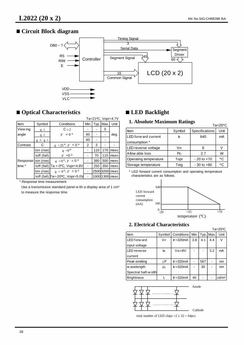
AN No.SIG-CHMO9805AL2022 (20 x 2)
Optical Characteristics
1. Absolute Maximum Ratings
2. Electrical Characteristics
LED Backlight
640
160
+25 +70
LED forwardcurrentconsumption(mA)
temperature (ºC)-20
0
Anode
Cathode
total number of LED chips =2 x 32 = 64pcs
* LED forward current consumption and operating temperature characteristics are as follows.
Ta=25ºC
Item Symbol Specifications Unit
LED forw ard current IF 640 mA
consumption *
LED reverse voltage VR 8 V
Allow able loss PD 2.7 W
Operating temperature Topr - 20 to +70 ºC
Storage temperature Tstg - 30 to +80 ºC
Ta=25ºC
Item Symbol Conditions Min. Typ. Max. Unit
LED forw ard VF IF=320mA 3.8 4.1 4.4 V
input voltage
LED reverse IR VR=8V - - 3.2 mA
current
Peak emitting λP IF=320mA - 567 - nm
w avelength δλ IF=320mA - 30 - nm
Spectral half-w idth
Brightness L IF=320mA 40 - - cd/m²
Ta=21ºC, Vopr=4.7V
Item Symbol Conditions Min. Typ. Max. Unit
View ing θ 1 C ≥ 2 - - 0
angle θ 2 Φ = 0 º 60 - - deg.
θ 2 - θ 1 60 - -
Contrast C θ = 25 º, Φ = 0 º 2 3 - -
ton (rise) θ =0 º - 110 170 msec
toff (fall) Φ =0 º - 70 110 msec
Response ton (rise) θ = 0 º, Φ = 0 º - 380 500 msec
time * toff (fall) Ta = 0ºC, Vopr=4.8V - 250 350 msec
ton (rise) θ = 0 º, Φ = 0 º - 2500 3200 msec
toff (fall) Ta=-20ºC, Vopr=5.0V - 1000 1300 msec
* Response time measurement
Use a transmissive standard panel w ith a display area of 1 cm²
to measure the response time
28
Timing Signal3
Common Signal
Serial Data
Segment Signal
16
60Controller
VDDVSSVLC
DB0 ~ 7
RSR/W
E
LCD (20 x 2)
40
SegmentDriver
Circuit Block diagram

AN No. SIG-CHMO9805A
20 Characters x 4 line5 x 7 Dot Matrix + Cursor1/16 Duty5V single Power SupplyAvailable in EL and LED Backlight type
L2014 (20 x 4)
Note : Only dimension changes between Reflective/EL and LED backlight is thickness.
Absolute Maximum Ratings
Electrical Characteristics
Mechanical Characteristics
Pin Function
Dimensions
VSS=0V, Ta=25ºC
Item Symbol Conditions Min. Max. Unit
Pow er supply VDD -0.3 6.0 V
voltage VLC -0.3 VDD V
Input voltage Vin -0.3 VDD +0.3 V
Operating temperature
Normal Topr 0 +50 ºC
Wide Topr -20 +70 ºC
Storage temperature
Normal Tstg -20 +60 ºC
Wide Tstg -30 +80 ºC
Storage < 48 hrs +20 +85 %RH
humidity <1000 hrs +20 +65 %RH
No. Name Function
1 VSS GND
2 VDD Pow er supply voltage +5V
3 VLC Liquid crystal driving voltage
4 RS L : Instruction code input
H: Data input
5 R/W L : Data w rite from MPU to LCM
H : Data read from LCM to MPU
6 E Enable
7 DB0 Data bus line
8 DB1 Data bus line
9 DB2 Data bus line
10 DB3 Data bus line
11 DB4 Data bus line
12 DB5 Data bus line
13 DB6 Data bus line
14 DB7 Data bus line
( 15 ) A Anode (+) for LED backlight
( 16 ) K Cathode (-) for LED backlight
Item Specifications Unit
Module size (H x V) 98.0 x 60.0 mm
Thickness Reflective/EL 11.6 mm
LED 15.8 mm
View ing area (H x V) 61.8 x 25.2 mm
Character size w ith cursor (H x V) 2.95 x 4.75 mm
Mounting hole distance (H x V) 93.0 x 55.0 mm
Reflective 55 g
Weight EL backlight 60 g
LED backlight 70 g
H : Horizontal, V : Vertical
VDD=5V± 5%, VSS=0V, Ta=0 ~ 50ºC
Item Symbol Conditions Min. Typ. Max. Unit
Pow er supply VDD 4.75 5.00 5.25 V
voltage VDD - VLC 3.0 - 6.3 V
Input High VIH1 2.2 - VDD V
voltage Low V IL1 0 - 0.6 V
Output High VOH1 -IOH=0.205mA 2.4 - - V
voltage Low VLH1 -IOL=1.2mA - - 0.4 V
Current consumption *
Normal Temp IDD Ta=25ºC - 2.6 3.5 mA
type ILC VLC=0.25V - 1.1 1.6 mA
Wide Temp. IDD Ta=25ºC - 2.8 3.5 mA
type ILC VLC=-0.6V - 1.4 2.2 mA
* test pattern : check board pattern
L2022 (2x20) Unit: mm, General tolerance ±0.5 mm
LED BacklightReflective/EL Backlight
29

AN No. SIG-CHMO9805AL2014 (20 x 4)
Optical Characteristics
2.Wide Temperature Range Type
1. Normal Temperature Range Type
1. Absolute Maximum Ratings
2. Electrical Characteristics
LED Backlight
520
130
+25 +70
LED forwardcurrentconsumption(mA)
temperature (ºC)-20
0
Anode
Cathode
total number of LED chips =2 x 26 = 52 pcs
* LED forward current consumption and operating temperature characteristics are as follows.
Ta=21ºC, 1/16 Duty, Vopr=4.75V
Item Symbol Conditions Min. Typ. Max. Unit
View ing θ 1 C ≥ 2 - - -15
angle θ 2 Φ = 0 º 55 - - deg.
θ 2 - θ 1 70 - -
Contrast C θ =+25 º, Φ = 0 º - 5 - -
ton (rise) θ =0 º - 150 200 msec
Response toff (fall) Φ =0 º - 200 220 msec
time ton (rise) θ = 0 º, Φ = 0 º - 750 800 msec
toff (fall) Ta = 0ºC, Vopr=5.0V - 600 700 msec
Measuring equipment : Canon illuminater LC-4SR
Ta=25ºC
Item Symbol Specifications Unit
LED forw ard current IF 520 mA
consumption *
LED reverse voltage VR 8 V
Allow able loss PD 2.28 W
Operating Temperature Topr - 20 ~ +70 ºC
Storage Temperature Tstg - 40 ~ + 80 ºC
Ta=25ºC
Item Symbol Conditions Min. Typ. Max. Unit
LED forw ard VF IF=260mA 3.8 4.1 4.4 V
input voltage
LED reverse IR VR=8V - - 0.2 mA
current
Peak emitting IR IF=260mA* - 570 - nm
w avelength
Spectral DI IF=260mA* - 30 - nm
half-w idth
Brightness L IF=260mA* 120 170 - cd/m²
Ta=21ºC, 1/16 Duty, Vopr=VDD - VLC
Item Symbol Conditions Min. Typ. Max. Unit
View ing θ 1 C ≥ 2 - - -15
angle θ 2 Φ = 0 º 55 - - deg.
θ 2 - θ 1 Vop=5,6v 70 - -
Contrast C θ =+20 º, Φ = 0 º - 5 - -
Vop=5,6v
ton (rise) θ = 0 º, Φ = 0 º - 150 200 msec
Response toff (fall) Ta = 21ºC, Vopr=5.6V - 200 220 msec
time ton (rise) θ = 0 º, Φ = 0 º - 750 800 msec
toff (fall) Ta = 0ºC, Vopr=5.9V - 600 700 msec
Measuring equipment : Canon illuminater LC-4SR
Circuit Block diagram
Recommended Operating VoltageThe recommended value (Vopr) for an ambient temperature
is as follow s. Vopr=VDD - VLC
Temperature (ºC) -20 0 +25 +50 +70
Vopr (V) Normal - 5.00 4.75 4.50 -
Wide 6.20 5.90 5.60 5.40 5.20
30
60 20
2080
16
16
Timing Signal3
Common Signal
Serial Data
Segment SignalController
VDDVSSVLC
DB0 ~ 7
RSR/W
E
LCD (20 x 4)
40
SegmentDriver
SegmentDriver

AN No. SIG-CHMO9805AL2014 (20 x 4)
1.Absolute Maximum Ratings
2. Brightness, Current, Life Characteristics
3.4 Inverter Dimensions (unit : mm)
Pin No. Function
1 Input : 5V DC
2 Common : GND
3 Output
EL Backlight
3.1 Electrical Characteristics (When combined with EL lamp)
3.2 Tolerance (Inverter only)
3.3 Maximum Ratings (Inverter only)
3. Suitable Inverter 5A
Item Symbol Standard Unit
Operating Vopr AC 150V, 1KHz V
voltage Sinew ave
Operating Topr - 10 ~ +50 ºC
temperature
Storage Tstg -20 ~ + 60 ºC
temperature
Storage 0 ~ 10 % RH (60 ºC)
humidity 0 ~ 30 % RH (40 ºC)
Item Conditions Specifications Unit
Brightness 100V, 400Hz 35 min. cd/m²
Sinew ave 45 typ.
Current 100V, 400Hz 3.0 typ. mA
Sinew ave 4.5 max
Life 100V, 400Hz, Sinew ave 1,500
25ºC,50%RH hrs
Using 5A Inverter 3,500
25ºC,50%RH
Item Specifications Unit
Input voltage 3.0 to 6.0 V
Load range 5 to 20 cm²
Item Specifications Unit
Input voltage 7.0 V
Load range 50 cm²
Operating temperature -10 to +60 ºC
Storage temperature -20 to +70 ºC
Ta=25ºC
Item Symbol Conditions Specifications Unit
Oscillating f INV V IN=5VDC 350 typ. Hz
frequency
Output voltage VOUT V IN=5VDC 95 typ. V
Output current IOUT V IN=5VDC 1.5 typ. mA
Input current V IN 5 Vrms
voltage IIN V IN=5VDC 45 typ mA
Initial brightness B V IN=5VDC 35 typ. cd/m²
17.5
± 1
4.5
10 16
1
23
3-∅ 0.7
16
10.5
7 ±
1
31

AN No. SIG-CHMO9805A
24 Characters x 2 line5 x 7 Dot Matrix + Cursor1/16 Duty5V single Power SupplyAvailable in EL and LED Backlight type
L2432 (24 x 2)
Note : Only dimension changes between Reflective/EL and LED backlight is thickness.
Absolute Maximum Ratings
Electrical Characteristics
Mechanical Characteristics
Pin Function
Dimensions
VSS=0V, Ta=25ºC
Item Symbol Conditions Min. Max. Unit
Pow er supply VDD -0.3 6.0 V
voltage VLC -0.3 VDD V
Input voltage Vin -0.3 VDD +0.3 V
Operating temperature
Normal Topr 0 +50 ºC
Wide Topr -20 +70 ºC
Storage temperature
Normal Tstg -20 +60 ºC
Wide Tstg -30 +80 ºC
Storage < 48 hrs +20 +85 %RH
humidity <1000 hrs +20 +65 %RH
No. Name Function
1 VSS GND
2 VDD Pow er supply voltage +5V
3 VLC Liquid crystal driving voltage
4 RS L : Instruction code input
H: Data input
5 R/W L : Data w rite from MPU to LCM
H : Data read from LCM to MPU
6 E Enable
7 DB0 Data bus line
8 DB1 Data bus line
9 DB2 Data bus line
10 DB3 Data bus line
11 DB4 Data bus line
12 DB5 Data bus line
13 DB6 Data bus line
14 DB7 Data bus line
( 15 ) A Anode (+) for LED backlight
( 16 ) K Cathode (-) for LED backlight
Item Specifications Unit
Module size (H x V) 118.0 x 36.0 mm
Thickness Reflective/EL 11.3 mm
LED 15.8 mm
View ing area (H x V) 94.5 x 17.8 mm
Character size w ith cursor (H x V) 3.20 x 5.55 mm
Mounting hole distance (H x V) 113.0 x 31.0 mm
Reflective 40 g
Weight EL backlight 45 g
LED backlight 60 g
H : Horizontal, V : Vertical
VDD=5V± 5%, VSS=0V, Ta=0 ~ 50ºC
Item Symbol Conditions Min. Typ. Max. Unit
Pow er supply VDD 4.75 5.00 5.25 V
voltage VDD - VLC 3.0 - 6.3 V
Input High VIH1 2.2 - VDD V
voltage Low V IL1 0 - 0.6 V
Output High VOH1 -IOH=0.205mA 2.4 - - V
voltage Low VLH1 -IOL=1.2mA - - 0.4 V
Current consumption *
Normal Temp IDD Ta=25ºC - 1.6 3.0 mA
type ILC VLC=0.25V - 0.4 1.2 mA
Wide Temp. IDD Ta=25ºC - 2.5 4.0 mA
type ILC VLC=-0.6V - 0.6 1.2 mA
* test pattern : check board pattern
L2432 (2x24) Unit: mm, General tolerance ±0.5 mm
LED Backlight
Reflective/EL Backlight
32

AN No. SIG-CHMO9805AL2432 (24 x 2)
Optical Characteristics
2.Wide Temperature Range Type
1. Normal Temperature Range Type
1. Absolute Maximum Ratings
2. Electrical Characteristics
LED Backlight
300
75
+25 +70
LED forwardcurrentconsumption(mA)
temperature (ºC)-20
0
Anode
Cathode
total number of LED chips =2 x 15 = 30 pcs
* LED forward current consumption and operating temperature characteristics are as follows.
Ta=21ºC, 1/16 Duty, Vopr=4.75V
Item Symbol Conditions Min. Typ. Max. Unit
View ing θ 1 C ≥ 2 - - -15
angle θ 2 Φ = 0 º 55 - - deg.
θ 2 - θ 1 70 - -
Contrast C θ =+25 º, Φ = 0 º - 5 - -
ton (rise) θ =0 º - 150 200 msec
Response toff (fall) Φ =0 º - 200 220 msec
time ton (rise) θ = 0 º, Φ = 0 º - 750 800 msec
toff (fall) Ta = 0ºC, Vopr=5.0V - 600 700 msec
Measuring equipment : Canon illuminater LC-4SR
Ta=25ºC
Item Symbol Specifications Unit
LED forw ard current IF 300 mA
consumption *
LED reverse voltage VR 8 V
Allow able loss PD 1.3 W
Operating Temperature Topr - 20 ~ +70 ºC
Storage Temperature Tstg - 40 ~ + 80 ºC
Ta=25ºC
Item Symbol Conditions Min. Typ. Max. Unit
LED forw ard VF IF=150mA 3.8 4.1 4.4 V
input voltage
LED reverse IR VR=8V - - 1.5 mA
current
Peak emitting IR IF=150mA* - 570 - nm
w avelength
Spectral DI IF=150mA* - 30 - nm
half-w idth
Brightness L IF=150mA* 40 50 - cd/m²
Ta=21ºC, 1/16 Duty, Vopr=VDD - VLC
Item Symbol Conditions Min. Typ. Max. Unit
View ing θ 1 C ≥ 2 - - -15
angle θ 2 Φ = 0 º 55 - - deg.
θ 2 - θ 1 Vop=5,6v 70 - -
Contrast C θ =+20 º, Φ = 0 º - 5 - -
Vop=5,6v
ton (rise) θ = 0 º, Φ = 0 º - 150 200 msec
Response toff (fall) Ta = 21ºC, Vopr=5.6V - 200 220 msec
time ton (rise) θ = 0 º, Φ = 0 º - 750 800 msec
toff (fall) Ta = 0ºC, Vopr=5.9V - 600 700 msec
Measuring equipment : Canon illuminater LC-4SR
Circuit Block diagram
Recommended Operating VoltageThe recommended value (Vopr) for an ambient temperature
is as follow s. Vopr=VDD - VLC
Temperature (ºC) -20 0 +25 +50 +70
Vopr (V) Normal - 5.00 4.75 4.50 -
Wide 6.20 5.90 5.60 5.40 5.20
Timing Signal3
Common Signal
Serial Data
Segment Signal
16
80Controller
VDDVSSVLC
DB0 ~ 7
RSR/W
E
LCD (24 x 2)
40
SegmentDriver
33

AN No. SIG-CHMO9805AL2432 (24 x 2)
1.Absolute Maximum Ratings
2. Brightness, Current, Life Characteristics
3.4 Inverter Dimensions (unit : mm)
Pin No. Function
1 Input : 5V DC
2 Common : GND
3 Output
EL Backlight
3.1 Electrical Characteristics (When combined with EL lamp)
3.2 Tolerance (Inverter only)
3.3 Maximum Ratings (Inverter only)
3. Suitable Inverter 5A
Item Symbol Standard Unit
Operating Vopr AC 150V, 1KHz V
voltage Sinew ave
Operating Topr - 10 ~ +50 ºC
temperature
Storage Tstg -20 ~ + 60 ºC
temperature
Storage 0 ~ 10 % RH (60 ºC)
humidity 0 ~ 30 % RH (40 ºC)
Item Conditions Specifications Unit
Brightness 100V, 400Hz 35 min. cd/m²
Sinew ave 45 typ.
Current 100V, 400Hz 2.2 typ. mA
Sinew ave 3.0 max
Life 100V, 400Hz, Sinew ave 1,500
25ºC,50%RH hrs
Using 5A Inverter 4,000
25ºC,50%RH
Item Specifications Unit
Input voltage 3.0 to 6.0 V
Load range 5 to 20 cm²
Item Specifications Unit
Input voltage 7.0 V
Load range 50 cm²
Operating temperature -10 to +60 ºC
Storage temperature -20 to +70 ºC
Ta=25ºC
Item Symbol Conditions Specifications Unit
Oscillating f INV V IN=5VDC 350 typ. Hz
frequency
Output voltage VOUT V IN=5VDC 95 typ. V
Output current IOUT V IN=5VDC 1.5 typ. mA
Input current V IN 5 Vrms
voltage IIN V IN=5VDC 45 typ mA
Initial brightness B V IN=5VDC 35 typ. cd/m²
17.5
± 1
4.5
10 16
1
23
3-∅ 0.7
16
10.5
7 ±
1
34

AN No.SIG-CHMO9805A
40 Characters x 2 line5 x 7 Dot Matrix + Cursor1/16 Duty5V single Power SupplyAvailable in EL and LED Backlight type
L4042 (40 x 2)
Note : Only dimension changes between Reflective/EL and LED backlight is thickness.
Absolute Maximum Ratings
Electrical Characteristics
Mechanical Characteristics
Pin Function
Dimensions
VSS=0V, Ta=25ºC
Item Symbol Conditions Min. Max. Unit
Pow er supply VDD -0.3 6.0 V
voltage VLC -0.3 VDD V
Input voltage Vin -0.3 VDD +0.3 V
Operating temperature
Normal Topr 0 +50 ºC
Wide Topr -20 +70 ºC
Storage temperature
Normal Tstg -20 +60 ºC
Wide Tstg -30 +80 ºC
Storage < 48 hrs +20 +85 %RH
humidity <1000 hrs +20 +65 %RH
No. Name Function
1 VSS GND
2 VDD Pow er supply voltage +5V
3 VLC Liquid crystal driving voltage
4 RS L : Instruction code input
H: Data input
5 R/W L : Data w rite from MPU to LCM
H : Data read from LCM to MPU
6 E Enable
7 DB0 Data bus line
8 DB1 Data bus line
9 DB2 Data bus line
10 DB3 Data bus line
11 DB4 Data bus line
12 DB5 Data bus line
13 DB6 Data bus line
14 DB7 Data bus line
( 15 ) A Anode (+) for LED backlight
( 16 ) K Cathode (-) for LED backlight
Item Specifications Unit
Module size (H x V) 182.0 x 33.5 mm
Thickness Reflective/EL 11.3 mm
LED 16.3 mm
View ing area (H x V) 154.4 x 15.8 mm
Character size w ith cursor (H x V) 3.20 x 5.55 mm
Mounting hole distance (H x V) 175.0 x 26.5 mm
Reflective 70 g
Weight EL backlight 75 g
LED backlight 95 g
H : Horizontal, V : Vertical
VDD=5V± 5%, VSS=0V, Ta=0 ~ 50ºC
Item Symbol Conditions Min. Typ. Max. Unit
Pow er supply VDD 4.75 5.00 5.25 V
voltage VDD - VLC 3.0 - 6.3 V
Input High VIH1 2.2 - VDD V
voltage Low V IL1 0 - 0.6 V
Output High VOH1 -IOH=0.205mA 2.4 - - V
voltage Low VLH1 -IOL=1.2mA - - 0.4 V
Current consumption *
Normal Temp IDD Ta=25ºC - 3.0 4.5 mA
type ILC VLC=0.25V - 1.0 1.5 mA
Wide Temp. IDD Ta=25ºC - 2.5 3.5 mA
type ILC VLC=-0.6V - 1.1 1.8 mA
* test pattern : check board pattern
L4042 (2x40) Unit: mm, General tolerance ±0.5 mm
LED Backlight
Reflective/EL Backlight
35

AN No.SIG-CHMO9805AL4042 (40 x 2)
Optical Characteristics
2.Wide Temperature Range Type
1. Normal Temperature Range Type
1. Absolute Maximum Ratings
2. Electrical Characteristics
LED Backlight
520
130
+25 +70
LED forwardcurrentconsumption(mA)
temperature (ºC)-20
0
Anode
Cathode
total number of LED chips =2 x 26 = 52 pcs
* LED forward current consumption and operating temperature characteristics are as follows.
Ta=21ºC, 1/16 Duty, Vopr=4.75V
Item Symbol Conditions Min. Typ. Max. Unit
View ing θ 1 C ≥ 2 - - -15
angle θ 2 Φ = 0 º 55 - - deg.
θ 2 - θ 1 70 - -
Contrast C θ =+25 º, Φ = 0 º - 5 - -
ton (rise) θ =0 º - 150 200 msec
Response toff (fall) Φ =0 º - 200 220 msec
time ton (rise) θ = 0 º, Φ = 0 º - 750 800 msec
toff (fall) Ta = 0ºC, Vopr=5.0V - 600 700 msec
Measuring equipment : Canon illuminater LC-4SR
Ta=25ºC
Item Symbol Specifications Unit
LED forw ard current IF 520 mA
consumption *
LED reverse voltage VR 8 V
Allow able loss PD 2.3 W
Operating Temperature Topr - 20 ~ +70 ºC
Storage Temperature Tstg - 40 ~ + 80 ºC
Ta=25ºC
Item Symbol Conditions Min. Typ. Max. Unit
LED forw ard VF IF=260mA 3.8 4.1 4.4 V
input voltage
LED reverse IR VR=8V - - 0.2 mA
current
Peak emitting IR IF=260mA* - 570 - nm
w avelength
Spectral DI IF=260mA* - 30 - nm
half-w idth
Brightness L IF=260mA* 120 150 - cd/m²
Ta=21ºC, 1/16 Duty, Vopr=VDD - VLC
Item Symbol Conditions Min. Typ. Max. Unit
View ing θ 1 C ≥ 2 - - -15
angle θ 2 Φ = 0 º 55 - - deg.
θ 2 - θ 1 Vop=5,6v 70 - -
Contrast C θ =+20 º, Φ = 0 º - 5 - -
Vop=5,6v
ton (rise) θ = 0 º, Φ = 0 º - 150 200 msec
Response toff (fall) Ta = 21ºC, Vopr=5.6V - 200 220 msec
time ton (rise) θ = 0 º, Φ = 0 º - 750 800 msec
toff (fall) Ta = 0ºC, Vopr=5.9V - 600 700 msec
Measuring equipment : Canon illuminater LC-4SR
Circuit Block diagram
Recommended Operating VoltageThe recommended value (Vopr) for an ambient temperature
is as follow s. Vopr=VDD - VLC
Temperature (ºC) -20 0 +25 +50 +70
Vopr (V) Normal - 5.00 4.75 4.50 -
Wide 6.20 5.90 5.60 5.40 5.20
8080
16
16
Timing Signal 3
Common Signal
Serial Data
Segment SignalController
VDDVSSVLC
DB0 ~ 7
RSR/W
E
LCD (40 x 2)
40
SegmentDriver
SegmentDriver
36

AN No.SIG-CHMO9805AL4042 (40 x 2)
1.Absolute Maximum Ratings
2. Brightness, Current, Life Characteristics
3.4 Inverter Dimensions (unit : mm)
Pin No. Function
1 Input : 5V DC
2 Common : GND
3 Output
EL Backlight
3.1 Electrical Characteristics (When combined with EL lamp)
3.2 Tolerance (Inverter only)
3.3 Maximum Ratings (Inverter only)
3. Suitable Inverter 5C
Item Symbol Standard Unit
Operating Vopr AC 150V, 1KHz V
voltage Sinew ave
Operating Topr - 10 ~ +50 ºC
temperature
Storage Tstg -20 ~ + 60 ºC
temperature
Storage 0 ~ 10 % RH (60 ºC)
humidity 0 ~ 30 % RH (40 ºC)
Item Conditions Specifications Unit
Brightness 100V, 400Hz 30 min. cd/m²
Sinew ave 40 typ.
Current 100V, 400Hz 4.0 typ. mA
Sinew ave 5.0 max
Life 100V, 400Hz, Sinew ave 1,500
25ºC,50%RH hrs
Using 5C Inverter 4,000
25ºC,50%RH
Item Specifications Unit
Input voltage 3.0 to 6.0 V
Load range 25 to 40 cm²
Item Specifications Unit
Input voltage 7.0 V
Load range 50 cm²
Operating temperature -10 to +60 ºC
Storage temperature -20 to +70 ºC
Ta=25ºC
Item Symbol Conditions Specifications Unit
Oscillating f INV V IN=5VDC 480 typ. Hz
frequency
Output voltage VOUT V IN=5VDC 105 typ. V
Output current IOUT V IN=5VDC 3.5 typ. mA
Input current V IN 5 VDC
voltage IIN V IN=5VDC 25 typ mA
Initial brightness B V IN=5VDC 45 typ. cd/m²
18.5
± 1
7±1
2
47.
6
221
23
3-∅ 0.7
16
10.5
37

AN No.SIG-CHMO9805A
40 Characters x 4 line5 x 7 Dot Matrix + Cursor1/16 Duty5V single Power SupplyAvailable in EL and LED Backlight type
M4024 (40 x 4)
Note : Only dimension changes between Reflective/EL and LED backlight is thickness.
Absolute Maximum Ratings
Electrical Characteristics
Mechanical Characteristics
Pin Function
Dimensions
VSS=0V, Ta=25ºC
Item Symbol Conditions Min. Max. Unit
Pow er supply VDD -0.3 6.0 V
voltage VLC -0.3 VDD V
Input voltage Vin -0.3 VDD +0.3 V
Operating temperature
Normal Topr 0 +50 ºC
Wide Topr -20 +70 ºC
Storage temperature
Normal Tstg -20 +60 ºC
Wide Tstg -30 +80 ºC
Storage < 48 hrs +20 +85 %RH
humidity <1000 hrs +20 +65 %RH
No. Name Function
1 DB0 Data bus line
2 DB1 Data bus line
3 DB2 Data bus line
4 DB3 Data bus line
5 DB4 Data bus line
6 DB5 Data bus line
7 DB6 Data bus line
8 DB7 Data bus line
9 E1 Enable (upper)
10 R/W H : Read, L : Write
11 RS H : Data Register
L : Instruction Register
12 VLC Liquid crystal driving voltage
13 VSS GND
14 VDD Pow er Suppy voltage: +%V
15 E2 Enable (Low er)
16 NC
(17) A Anode (+) for LED backlight
(18) K Cathode (-) for LED backlight
Item Specifications Unit
Module size (H x V) 190.0 x 54.0 mm
Thickness Reflective/EL 10.1 mm
LED 16.3 mm
View ing area (H x V) 147.0 x 29.5 mm
Character size w ith cursor (H x V) 2.78 x 4.89 mm
Mounting hole distance (H x V) 183.0 x 47.0 mm
Reflective 90 g
Weight EL backlight 105 g
LED backlight 140 g
H : Horizontal, V : Vertical
VDD=5V± 5%, VSS=0V, Ta=0 ~ 50ºC
Item Symbol Conditions Min. Typ. Max. Unit
Pow er supply VDD 4.75 5.00 5.25 V
voltage VDD - VLC 3.0 - 6.3 V
Input High VIH1 2.2 - VDD V
voltage Low V IL1 0 - 0.6 V
Output High VOH1 -IOH=0.205mA 2.4 - - V
voltage Low VLH1 -IOL=1.2mA - - 0.4 V
Current consumption *
Normal Temp IDD Ta=25ºC - 8.0 12.0 mA
type ILC VLC=0.25V - 3.8 4.5 mA
Wide Temp. IDD Ta=25ºC - 7.9 9.0 mA
type ILC VLC=-0.6V - 4.5 6.0 mA
* test pattern : check board pattern
M4024 (4x40) Unit: mm, General tolerance ±0.5 mmLED Backlight
Reflective/EL Backlight
38

AN No.SIG-CHMO9805AM4024 (40 x 4)
Optical Characteristics
2.Wide Temperature Range Type
1. Normal Temperature Range Type
1. Absolute Maximum Ratings
2. Electrical Characteristics
LED Backlight
1000
250
+25 +70
LED forwardcurrentconsumption(mA)
temperature (ºC)-20
0
Anode
Cathode
total number of LED chips =2 x 50 = 100 pcs
* LED forward current consumption and operating temperature characteristics are as follows.
Ta=21ºC, 1/16 Duty, Vopr=4.75V
Item Symbol Conditions Min. Typ. Max. Unit
View ing θ 1 C ≥ 2 - - -15
angle θ 2 Φ = 0 º 55 - - deg.
θ 2 - θ 1 70 - -
Contrast C θ =+25 º, Φ = 0 º - 5 - -
ton (rise) θ =0 º - 150 200 msec
Response toff (fall) Φ =0 º - 200 220 msec
time ton (rise) θ = 0 º, Φ = 0 º - 750 800 msec
toff (fall) Ta = 0ºC, Vopr=5.0V - 600 700 msec
Measuring equipment : Canon illuminater LC-4SR
Ta=25ºC
Item Symbol Specifications Unit
LED forw ard current IF 1000 mA
consumption *
LED reverse voltage VR 8 V
Allow able loss PD 4.4 W
Operating Temperature Topr - 20 ~ +70 ºC
Storage Temperature Tstg - 40 ~ + 80 ºC
Ta=25ºC
Item Symbol Conditions Min. Typ. Max. Unit
LED forw ard VF IF=500mA 3.8 4.1 4.4 V
input voltage
LED reverse IR VR=8V - - 0.2 mA
current
Peak emitting IR IF=500mA* - 570 - nm
w avelength
Spectral DI IF=500mA* - 30 - nm
half-w idth
Brightness L IF=500mA* 120 170 - cd/m²
Ta=21ºC, 1/16 Duty, Vopr=VDD - VLC
Item Symbol Conditions Min. Typ. Max. Unit
View ing θ 1 C ≥ 2 - - -15
angle θ 2 Φ = 0 º 55 - - deg.
θ 2 - θ 1 Vop=5,6v 70 - -
Contrast C θ =+20 º, Φ = 0 º - 5 - -
Vop=5,6v
ton (rise) θ = 0 º, Φ = 0 º - 150 200 msec
Response toff (fall) Ta = 21ºC, Vopr=5.6V - 200 220 msec
time ton (rise) θ = 0 º, Φ = 0 º - 750 800 msec
toff (fall) Ta = 0ºC, Vopr=5.9V - 600 700 msec
Measuring equipment : Canon illuminater LC-4SR
Circuit Block diagram
Recommended Operating VoltageThe recommended value (Vopr) for an ambient temperature
is as follow s. Vopr=VDD - VLC
Temperature (ºC) -20 0 +25 +50 +70
Vopr (V) Normal - 5.00 4.75 4.50 -
Wide 6.20 5.90 5.60 5.40 5.20
39
Segment Sigal
16
16
80 80Segment Sigal
Timing Signal 3
Serial Data
Common Sigal
Serial Data
Timing Signal 3
DB0 ~ 7
8080
Controller1
SegmentDriver
SegmentDriver
LCD (40 x 4)
40
SegmentDriver
Controller2
40
SegmentDriver
RSR/WE1
E2
DB0 ~ 7
VDDVSSVLC

AN No.SIG-CHMO9805AM4024 (40 x 4)
1.Absolute Maximum Ratings
2. Brightness, Current, Life Characteristics
3.4 Inverter Dimensions (unit : mm)
Pin No. Function
1 Input : 5V DC
2 Common : GND
3 Output
EL Backlight
3.1 Electrical Characteristics (When combined with EL lamp)
3.2 Tolerance (Inverter only)
3.3 Maximum Ratings (Inverter only)
3. Suitable Inverter 5D
Item Symbol Standard Unit
Operating Vopr AC 150V, 1KHz V
voltage Sinew ave
Operating Topr - 10 ~ +50 ºC
temperature
Storage Tstg -20 ~ + 60 ºC
temperature
Storage 0 ~ 10 % RH (60 ºC)
humidity 0 ~ 30 % RH (40 ºC)
Item Conditions Specifications Unit
Brightness 100V, 400Hz 30 min. cd/m²
Sinew ave 35 typ.
Current 100V, 400Hz 5.8 typ. mA
Sinew ave 8.0 max
Life 100V, 400Hz, Sinew ave 1,500
25ºC,50%RH hrs
Using 5D Inverter 3,500
25ºC,50%RH
Item Specifications Unit
Input voltage 3.0 to 6.0 V
Load range 35 to 60 cm²
Item Specifications Unit
Input voltage 7.0 V
Load range 50 cm²
Operating temperature -10 to +60 ºC
Storage temperature -20 to +70 ºC
Ta=25ºC
Item Symbol Conditions Specifications Unit
Oscillating f INV V IN=5VDC 350 typ. Hz
frequency
Output voltage VOUT V IN=5VDC 130 typ. V
Output current IOUT V IN=5VDC 5.5 typ. mA
Input current V IN 5 Vrms
voltage IIN V IN=5VDC 80 typ mA
Initial brightness B V IN=5VDC 45 typ. cd/m²
20.5
38
221
23
3-∅0.7
16
10
6±1
40

AN No.SIG-CHMO9805AOperating Instructions
VDD=5V ± 10%. VSS=0V, Ta=25ºC
Item Symbol Min. Max. Unit
Enabel cycle time tc 500 - ns
Enable rise time tr - 25 ns
Enable fall time tf - 25 ns
Enable pulse w idth tw 220 - ns
Setup time R/W, RS tSU1 40 - ns
Hold time R/S, RS th1 10 - ns
Data setup time tSU2 60 - ns
Data hold time th2 10 - ns
VDD=5V ± 10%. VSS=0V, Ta=25ºC
Item Symbol Min. Max. Unit
Enabel cycle time tc 500 - ns
Enable rise time tr - 25 ns
Enable fall time tf - 25 ns
Enable pulse w idth tw 220 - ns
Setup time R/W, RS tSU 40 - ns
Hold time R/S, RS th 10 - ns
Data delay time tD - 120 ns
Data hold time tDH 10 - ns
1. Timing Characteristics1.1 Write operation 1.2 Read operation
tc
RS
R/W
E
DB0 - DB7 Valid Data
tSU1
tW
V IH
V IL1
V IL1
V IH
V IL1
V IL
V IH
V IH
V IH
V IH1
V IL
V IL
V IL1
V IL1
V IL1
tSU2
tf
th1
th1
thtf
tSU th
RS
R/W
E
DB0 - DB7 Valid Data
tW
V IH1
V IL1
V IL1
V IH1
V IL1
V IL
V IH
V IH1
V IH
V IH1
V IL1
V ILV IL1
V IL1
tD
tf
tc
tDH
V IHth
t
2. Basic Operation2.1 Block Diagram of Controller KS0066
8 8
40
16
4
4
7
7
7
Commonsignal
(C1 - 16)16
7
8
4040
Input OutputBuffer
Busy Flag
40-bitShift
Register
40-bitShift
Register
40-bitShift
Register
CharacterGenerator
ROM(CG ROM)8320 bits
CharacterGenerator
RAM(CG RAM)512 bits
CursorBlink
ControlCircuit
DataRegister
(DR)
InstructionRegister
(IR)
AddressCounter (AC)
Display Data RAM(DD RAM)80x8 bits
InstructionDecoder
(IR)
16-bitShift
Register
16-bitShift
Register
Parallel/SerialData conversion
Circuit
DB0 ~ 3
DB4 ~ 7
R/WRS
E
Pow er supply for LCD drive
V1
V2
V3
V4
V5
D
8
7
7
8
8
CLK1CLK2M
VDD
VSS
TimingGeneration
Circuit
41

AN No.SIG-CHMO9805AOperation Instruction
2.2 RegistersThe controller (KS0066) has to kinds of eight-bit registers ; the instruction register (IR) and the data register (DR). They are selected bythe register select (RS) signal as shown below table 1. The IR stores instruction codes such as Display Clear and Cursor Home, and theaddress information of display data RAM (DD RAM) and character generator RAM (CG RAM). They can be written from the MPU, butcan not be read to the MPU. The DR temporarily stores data to be written into DD RAM or CG RAM, or data read from D RAM or CGRAM. For data write, the data written into the DR from the MPU is automatically written into DD RAM or CG RAM by internal operation.For data read, when the data address is written into the IR, the specified data is read out to the DR by internal operation. Then the MPUreads it from the DR. After the read operation, the next address is set and DD RAM or CG RAM data at the address is read into the DRfor the next read operation.
2.3 Busy Flag (BF)The busy flag indicates whether the module is ready to accept the next instruction. As shown in table, the signal is output to DB7, ifRS=0 and R/W=1. If the busy flag is 0, the next instruction can be written. Therefore, the busy flag status needs to be checked beforeexecuting an instruction. To execute an instruction without checking the flag status, wait for more than the execution time of priorinstruction. For the execution time of each instruction, see section 3 “Instruction Outline”.
2.4 Address Counter (AC)The address counter specifies an address when data is written into DD RAM or CG RAM and when the data stored in DD RAM or CGRAM is read out. If an address Set instruction (for DD RAM orCG RAM) is written into IR, the address information is transferred from theIR to the AC. When display data is written into or read from DD RAM or CG RAM, the AC is automatically incremented or decrementedby one according to the Entry Mode Set. The contents of the AC are output to DB0 to DB6 if RS=0 and R/W=1 as shown in table 1.
2.5 Display Data RAM (DD RAM) DD RAM has a capacity of up to 80 x 8 bits and stores display data of 80 eight-bit character codes. Some storage areas of DD RAM thatare not used for display can be used as general data RAM. A DD RAM address to be set in the AC is expressed in hexadecimal form asfollows. Example : DD RAM address “07”The correspondence between the DD RAM address and the display digits of the LCD panel is described in the followings.
AC : AC6 AC5 AC4 AC3 AC2 AC1 AC0
0 0 0 0 1 1 1
Low er bitUpper bit
0 7
2.6 Address LocationThe DD RAM address and the display digit of the LCD panel correspond as follows for LCD modules driven by 1/16duty and onecontroller can display maximum 80 characters.
When the display digits are less than 40, the display begins at the head positions of the two lines. In this case, first line end addressand the second line start address are not consecutive.
2.6.1 M1641
Note : This is initialised as a 2 line display because of no LCD driver. Character No.9 must be addressed as first position of 2nd line,which is 40 (HEX).
2.6.2 M1632, L1642, L1652
2.6.3 L1614
1 2 3 15 16 17 18 19 20 38 39 40 Display digit
Line 1 00 01 02 0E 0F 10 11 12 13 25 26 27 DD RAM
Line 2 40 41 42 4E 4F 50 51 52 53 65 66 67 address (HEX)
1 2 3 4 5 6 7 8 9 10 11 12 13 14 15 16 Display digit
Line 1 00 01 02 03 04 05 06 07 40 41 42 43 44 45 46 47 DD RAM address (HEX)
1 2 3 4 5 6 7 8 9 10 11 12 13 14 15 16 Display digit
Line 1 00 01 02 03 04 05 06 07 08 09 0A 0B 0C 0D 0E 0F DD RAM
Line 2 40 41 42 43 44 45 46 47 48 49 4A 4B 4C 4D 4E 4F address (HEX)
1 2 3 4 5 6 7 8 9 10 11 12 13 14 15 16 Display digit
Line 1 00 01 02 03 04 05 06 07 08 09 0A 0B 0C 0D 0E 0F
Line 2 40 41 42 43 44 45 46 47 48 49 4A 4B 4C 4D 4E 4F DD RAM
Line 3 10 11 12 13 14 15 16 17 18 19 1A 1B 1C 1D 1E 1F address (HEX)
Line 4 50 51 52 53 54 55 56 57 58 59 5A 5B 5C 5D 5E 5F
Table 1 Register Selection RS R/W Operation
0 0 IR selection, IR w rite. Internal operation : Display Clear, Cursor Home, etc
0 1 Busy flag (DB7) and address counter (DB0 to DB6) read
1 0 DR selection, DR w rite. Internal operation : DR to DD RAM or to CG RAM
1 1 DR selection, DR read. Internal operation : DD RAM or CG RAM to DR
42

AN No.SIG-CHMO9805AOperation Instruction
2.6.5 L2014
Consequently, the end address of line 1 and the start address of line 3 are consecutive. Also, the end address of line 2 and the startaddress of line 4 are consecutive. The DD RAM address 00H to 27H are displayed in line 1 and line 3 and 40H to 67H in line 2 and line 4by executing Display Shift
2.6.6 L2432
2.6.3 L4042
2.6.4 M4024
M4024 has two LCD controllers. Since the capacity for each is 80 characters (40 characters x 2 lines), M4024 can display 160characters (40 characters x 4 lines) by using two LCD controllers. Line 1 and 2 are activated by E1. Line 3 and 4 are activated by E2. Allthe four lines cannot be shifted at the same time. Instructions must be written using E1 and E2 to distinguish the upper two lines from thelower two lines.
1 2 3 4 5 6 7 8 9 10 11 12 13 14 15 16 17 18 19 20 Display digit
Line 1 00 01 02 03 04 05 06 07 08 09 0A 0B 0C 0D 0E 0F 10 11 12 13Line 2 40 41 42 43 44 45 46 47 48 49 4A 4B 4C 4D 4E 4F 50 51 52 53 DD RAM
Line 3 14 15 16 17 18 19 1A 1B 1C 1D 1E 1F 20 21 22 23 24 25 26 27 address (HEX)
Line 4 54 55 56 57 58 59 5A 5B 5C 5D 5E 5F 60 61 62 63 64 65 66 67
1 2 3 4 5 6 7 8 9 10 11 12 13 14 15 16 17 18 19 20 21 22 23 24 Display digit
Line 1 00 01 02 03 04 05 06 07 08 09 0A 0B 0C 0D 0E 0F 10 11 12 13 14 15 16 17 DD RAM
Line 2 40 41 42 43 44 45 46 47 48 49 4A 4B 4C 4D 4E 4F 50 51 52 53 54 55 56 57 address (HEX)
1 2 3 15 16 17 18 19 20 38 39 40 Display digit
Line 1 00 01 02 0E 0F 10 11 12 13 25 26 27 DD RAM
Line 2 40 41 42 4E 4F 50 51 52 53 65 66 67 address (HEX)
1 2 3 15 16 17 18 19 20 38 39 40 Display digit
Line 1 00 01 02 0E 0F 10 11 12 13 25 26 27
Line 2 40 41 42 4E 4F 50 51 52 53 65 66 67 DD RAM
Line 3 00 01 02 0E 0F 10 11 12 13 25 26 27 address (HEX)
Line 4 40 41 42 4E 4F 50 51 52 53 65 66 67
2.7 Character Generator ROM (CG ROM)CG ROM generates 5x7 dot-matrix character patterns from eight-bit character codes. In LCD modules of 5x7 dot-matrix characterpattern, CG generates 192 types of 5x7 characters. Table 2 shows the correspondence between the CG ROM character codes andcharacter patterns of 5x7 dot-matrix.
2.8 Character Generator RAM (CG RAM)CG RAM is used to create character patterns freely by program. Eight types of 5x7 dot-matrix character patterns can be written into aCG RAM. Table 3 shows the character patterns created from CG RAM addresses and CG RAM data. To display a created characterpattern, the character code in the left column of the table is written into DD RAM corresponding to the display position (digit). The areasnot used for display are available as general data RAM.
2.9 Cursor/Blink Control CircuitThe circuit generates the cursor or blink. When the address counter (AC) selects the address of DD RAM, the cursor or the blink appearsin the digit corresponding to the address. When the address counter is 08H, a cursor or blink position is in the 9th digit in line 1 as shownbelow.The cursor or blink also appears when the character generator RAM (CG RAM) is selected by the address counter. In this case, thecursor or blink position has no meaning.
AC6 AC5 AC4 AC3 AC2 AC1 AC0
AC 0 0 0 1 0 0 0
1 2 3 4 5 6 7 8 9 10 11 12 13 14 15 16 Display digit
Line 1 00 01 02 03 04 05 06 07 08 09 0A 0B 0C 0D 0E 0F DD RAM
Line 2 40 41 42 43 44 45 46 47 48 49 4A 4B 4C 4D 4E 4F address (HEX)
1 2 3 4 5 6 7 8 9 10 11 12 13 14 15 16 17 18 19 20 Display digit
Line 1 00 01 02 03 04 05 06 07 08 09 0A 0B 0C 0D 0E 0F 10 11 12 13 DD RAM
Line 2 40 41 42 43 44 45 46 47 48 49 4A 4B 4C 4D 4E 4F 50 51 52 53 address (HEX)
Consequently, the end address of line 1 and the start address of line 3 are consecutive. Also, the end address of line 2 and the startaddress of line 4 are consecutive. The DD RAM address 00H to 27H are displayed in line 1 and line 3 and 40H to 67H in line 2 and line 4by executing Display Shift.
2.6.4 L2012, L2022
43

AN No.SIG-CHMO9805AOperation Instruction
0101Upper 4 bits
XXXX0000
XXXX0001
XXXX0010
XXXX0011
XXXX0100
XXXX0101
XXXX0110
XXXX0111
XXXX1000
XXXX1001
XXXX1010
XXXX1011
XXXX1100
XXXX1101
XXXX1110
XXXX1111
CGRAM(1)
(8)
(7)
(6)
(5)
(4)
(3)
(2)
(1)
(8)
(7)
(6)
(5)
(4)
(2)
(3)
Low er 4 bits0000 0010 0011 0100 0110 0111 1010 1011 1100 1101 1110 11111000 1001
Table 2 Correspondence between character codes and character pattern (5x7 dot -matrix)
44

AN No.SIG-CHMO9805AOperation Instruction
7 6 5 4 3 2 1 0 5 4 3 2 1 0 7 6 5 4 3 2 1 0
0 0 0 * * * 1 1 1 1 0
0 0 1 1 0 0 0 1
0 1 0 1 0 0 0 1
0 0 0 0 * 0 0 0 0 0 0 0 1 1 1 1 1 1 0
1 0 0 1 0 1 0 0
1 0 1 1 0 0 1 0
1 1 0 1 0 0 0 1
1 1 1 * * * 0 0 0 0 0
0 0 0 * * * 1 0 0 0 1
0 0 1 0 1 0 1 0
0 1 0 1 1 1 1 1
0 1 1 0 0 1 0 0
0 0 0 0 * 0 0 1 0 0 1 1 0 0 1 1 1 1 1
1 0 1 0 0 1 0 0
1 1 0 0 0 1 0 0
1 1 1 * * * 0 0 0 0 0
0 0 0 * * *
0 0 1
0 1 0
0 0 0 0 * 1 1 1 1 1 1 1 0 0
1 0 1
1 1 0
1 1 1 * * *
Upper bit
CG RAM AddressCharacter Pattern(CG RAM data)
Character Code(DD RAM data)
Upper bit Upper bitLow er bit
Low er bitLow er bit
Table 3 Relation between CG RAM addresses and character codes (DD RAM) and character patterns (CG RAM) (5x7 dot-matrix)
Example of character pattern (R) and (¥ )* : don’t care bit
Notes : - In CG RAM data, “1” corresponds to Selection and “0” to Non-selection on the display.- Character code bits 0 to 2 and CG RAM address bits 3 to 5 correspond to each other (three bits, eight bytes).- CG RAM address bits 0 to 2 specify a line position for a character pattern, Line 8 of a character pattern is the cursor
position where the logical OR of the cursor and CG RAM data is displayed. Set the data of line 8 to “0” to display the cursor. If the data is changed to “1” , bit 1 lights, regardless of the cursor.
- The character pattern column positions correspond to CG RAM data bits 0 to 4 and bit 4 comes to the left end. CG RAM data bits 5 to 7 are not displayed but can be used as general data RAM.- When regarding a character pattern from CG RAM, set to “0” all of character code bits 4 to 7. Bits 0 to 2 determine which pattern will be read out. Since bit 3 is not valid, 00H and 08H select the same character.
45

AN No.SIG-CHMO9805A
3. Instruction Outline
Operation Instruction
When MPU controls LCD controller on the LCD module, MPU directly controls only two registers of the controllers; the InstructionRegister (IR) and the Data Register (DR). Prior to internal operation start, the controller temporarily stores control information in theseregisters, so as to interface with various types of MPUs or peripheral control ICs which operate at different speeds from speed ofcontroller internal operation.Table 4 shows the instructions and their execution time.While the controller is executing an instruction and internal operation is in progress, the controller will accept and execute no instructionother than the Busy Flag/Address Read instruction.Since the busy flag is set to “1” while an instruction is being executed, check the busy flag status and make sure it is “0” before sendingan instruction from the MPU to the controller.To send instructions without checking the busy flag, make sure that the interval between two instructions is much longer than theexecution time of the prior instruction.After the execution of writing/reading data instruction to/from CG/DD RAM, RAM address counter is automatically incremented ordecrement by one. This increment/decrement / is executed after the busy flag is set to “0”. The time from the fall edge of busy flag to theend of address counter renewal (tADD) is as shown below.
tADD
A
Busy state
tADD depends on the clock oscillation frequency (fosc)tADD = 1.5 (s) fosc
A+1
Busy signal (DB7)
Address counter(DB0 to DB6)
4. Initialization 4.1 Automatic InitialisationThe system is automatically initialised at power-on if the following power supply conditions are satisfied.
In automatic initialisation, the following instructions are executed. * Display Clear * Function Set
DL = 1 : Interface data length : Eight bitsN = 0, F = 0 : 1/8 duty, character font : 5 x 7 dot-matrix
* Display ON/OFF controlD = 0 : Display OFFC = 0 : Cursor OFFB = 0 : Blink OFF
* Entry Mode SetI/D = 1 : IncrementS = 0 : No display shift
Since some conditions set by initialisation may not be suitable for the LCD module, execute further Function Set instruction.The busy flag (BF) is kept busy until initialisation ends. The busy state remains for 20ms after VDD reaches to 4.5V.If the power supply conditions are not satisfied and automatic initialisation is not executed. Execute initialisation using instructionaccording to section 4.2, “Initialisation by Instruction”.
trcc
0.2V0.2V 0.2V4,5V
tOFF*
VDD
VSS
0,1ms ≤ trcc ≤ 10ms tOFF ≥ 1ms
tOFF* : Time w hen pow er supply is OFF if cut instantaneously or turned ON and OFF repeatedly
4.2 Initialisation by InstructionIf automatic initialisation is not executed because the power supply conditions are not satisfied, use interface data length of eight bits orfour bits instructions shown in table 4 and table 5 to implement initialisation.Since it is unknown whether the interface data length is set to eight bits or four bits at power on, execute Function Set twice to set theinterface data length to eight bits and then set the required interface data length by executing further Function Set instruction.
46

AN No.SIG-CHMO9805AOperating Instruction
Table 4 List of Instruction
Code Execution
RS R/W DB7 DB6 DB5 DB4 DB3 DB2 DB1 DB0 time **
Clears all display and returns cursor to
(1) Display Clear 0 0 0 0 0 0 0 0 0 1 home position (address 0) 1,64 ms
Returns cursor to home position, shifted
(2) Cursor Home 0 0 0 0 0 0 0 0 1 * display returns to home position and DD 1,64 ms
RAM contents do not change
Sets direction of cursor movement and
(3) Entry Mode Set 0 0 0 0 0 0 0 1 I/D S w hether display w ill be shifted w hen 40 µm
data is w ritten or read
Turns ON/OFF total display (D) and
(4) Display ON/OFF 0 0 0 0 0 0 1 D C B cursor (C), and makes cursor position 40 µm
Control column start blinking (B)
Moves cursor and shifts display w ithout
(5) Cursor/Display 0 0 0 0 0 1 S/C R/L * * changing DD RAM contents. 40 µm
Shift
Sets interface data length (DL), the
(6) Function Set 0 0 0 0 1 DL N F * * duty (N), and character fonts (F) 40 µm
Sets CG RAM address to start
(7) CG RAM Address 0 0 0 1 ACG transmitting or receiving CG RAM data 40 µm
Set
Sets DD RAM address to start
(8) DD RAM Address 0 0 1 ADD transmitting or receiving DD RAM data 40 µm
Set
Reads BF indicating module in internal
(9) BF/Address Read 0 1 BF AC operation and AC contents (use for both 0 µm
CG RAM and DD RAM)
(10) Data Write to
CG RAM or 0 1 Write Data Writes data into DD RAM or CG RAM 40 µm
DD RAM tADD=6µm
(11) Data Read from
CG RAM or 1 1 Read Data Reads data from DD RAM or CG RAM 40 µm
DD RAM tADD=6µm
* : Don't care bit I/D = 1 : Increment B = 1 : Blink ON N = 1 : 1/16 duty
ACG : CG RAM address I/D = 0 : Decrement B = 0 : Blink OFF N = 0 : 1/8 duty or 1/11 duty
ADD : DD RAM address
AC : Address counter S = 1 : Display shift S/C = 1 : Display shift F = 1 : 5 x 10 dot matrix
S = 0 : No display shift S/C = 0 : Cursor movement F = 0 : 5 x 7 dot matrix
D = 1 : Display ON R/L = 1 : Right shift BF = 1 : Internal operation in progress
D = 0 : Display OFF R/L = 0 : Left shift: BF = 0 : Instruction can be accepted
C = 1 : Cursor ON DL = 1 : 8 bits
C = 0 : Cursor OFF DL = 0 : 4 bits
** Execution time in the above Table indicated the maximum value w hen fosc is 250KHz. It changes w hen fosc changes.
When fosc = 270 KHz : 40 µs x 250 / 270 = 37 µs
FunctionInstruction
47

AN No.SIG-CHMO9805AOperating Instruction
RS R/W DB7 DB6 DB5 DB4 DB3 DB2 DB1 DB0 The busy flag cannot be checked from the follow ing instruction
0 0 0 0 1 1 * * * * Functon set (interface data length : 8 bits)
RS R/W DB7 DB6 DB5 DB4 DB3 DB2 DB1 DB0 The busy flag cannot be checked from the follow ing instruction
0 0 0 0 1 1 * * * * Functon set (interface data length : 8 bits)
RS R/W DB7 DB6 DB5 DB4 DB3 DB2 DB1 DB0 The busy flag cannot be checked from the follow ing instruction
0 0 0 0 1 1 * * * * Functon set (interface data length : 8 bits)
RS R/W DB7 DB6 DB5 DB4 DB3 DB2 DB1 DB0 The busy flag can be checked from the follow ing instruction
0 0 0 0 1 1 NF * * * Functon set (interface data length : 8 bits)
0 0 0 0 0 0 1 0 0 0 Display OFF
0 0 0 0 0 0 0 0 0 1 Display Clear
0 0 0 0 0 0 0 1 I/D S Entry Mode Set
Wait for 45 ms or more after VDD reaches 4,5V
Wait for 4,1 ms or more
Wait for 100 µs or more
End of initialisation
Power ON
Table 5. Interface Data Length : Eight bits
48

AN No.SIG-CHMO9805AOperating Instruction
Table 6. Interface Data Length : Four bits
RS R/W DB7 DB6 DB5 DB4 The busy flag cannot be checked from the follow ing instruction
0 0 0 0 1 1 Functon set (interface data length : 4 bits)
RS R/W DB7 DB6 DB5 DB4 The busy flag cannot be checked from the follow ing instruction
0 0 0 0 1 1 Functon set (interface data length : 4 bits)
RS R/W DB7 DB6 DB5 DB4 The busy flag cannot be checked from the follow ing instruction
0 0 0 0 1 1 Functon set (interface data length : 4 bits)
RS R/W DB7 DB6 DB5 DB4 The busy flag can be checked from the follow ing instruction
0 0 0 0 1 0 Functon set (interface data length : 4 bits)
0 0 0 0 1 0 Function Set
0 0 N F * *
0 0 0 0 0 0 Display OFF
0 0 1 0 0 0
0 0 0 0 0 0 Display Clear
0 0 0 0 0 1
0 0 0 0 0 0 Entry Mode Set
0 0 0 1 I/D S
Note : in M4024, execute initialisation on E1 and E2 respectively
Wait for 45 ms or more after VDD reaches 4,5V
Wait for 4,1 ms or more
Wait for 100 µs or more
End of initialisation
Power ON
49

AN No.SIG-CHMO9805AOperating Instruction
5. Instruction Detail
2.5.1 Display Clear
Display CLEAR clears all display and returns cursor to home position (address 0). Space code 20H is written into all the addresses ofDD RAM, and DD RAM address 0 is set to the AC, if it was shifted, the display returns to the original position. The cursor or blink go tothe left end on line 1, except M4024. In M4024, if the cursor or blink is on line 3 or line 4, it returns to the left end of line 3. After executionof the Display Clear instruction, I/D = 1 (increment) of Entry Mode is set.
RS R/W DB7 DB6 DB5 DB4 DB3 DB2 DB1 DB0
Code 0 0 0 0 0 0 0 0 0 1
2.5.2 Cursor Home
CURSOR Home returns cursor to home position (address 0). DD RAM address 0 is set to the AC. The display returns to the originalposition if it was shifted. The DD RAM contents do not change. If the cursor or blinking is ON, it returns to the left end, except M4024. InM4024, if the cursor or blink on line 3 or line 4, it returns to the left end of line 3.
RS R/W DB7 DB6 DB5 DB4 DB3 DB2 DB1 DB0
Code 0 0 0 0 0 0 0 0 1 *
2.5.3 Entry Mode Set
ENTRY Mode Set sets the direction of cursor movement and determines whether display is shifted.I/D :The DD RAM address is incremented or decremnted by one when a character code is written into or read from DD RAM. This is also true for writing into or reading from CG RAM. When I/D = 1, the address is incremented by one and the cursor or blink moves to the right. When I/D = 0, the address is decremented by one and the cursor or blink moves to the left.S : If S = 1, the entire display is shifted either to the right or left for writing into DD RAM. The cursor position does not changed only the
display moves, There is no display shift for reading form DD RAM.When S = 1 and I/D = 1, the display shifts one digit to the left after data write to DD RAM.When S = 1 and I/D = 0, the display shifts one digit to the right after data write to DD RAM.If S = 0, the display does not shift.
RS R/W DB7 DB6 DB5 DB4 DB3 DB2 DB1 DB0
Code 0 0 0 0 0 0 0 1 I/D S
2.5.4 Display ON/OFF Control
Display ON/OFF Control turns the total display and the cursor ON and OFF, and makes the character on the cursor position startblinking Cursor ON/OFF and blinking is done at the digit indicated by the DD RAM address specified by the ACD : When D = 1, the display is turned ON
When D = 0, the display is turned OFFIf D = 0 is used, display data remains in DD RAM. Therefore the data can be displayed again by setting D = 1.
C : When C = 1, the cursor is displayedWhen C = 0, the cursor is not displayed.The cursor is displayed in the dot line below the character fonts.
B : When B = 1, the character at the cursor position starts blinking.When B = 0, it does not blink.For blinking, all-black dots and the character are switched about every 0.4 seconds when fosc is 250KHz. The cursor and blinkingcan be set at the same time. * C =1 (cursor display) * B = 1 (blink)
RS R/W DB7 DB6 DB5 DB4 DB3 DB2 DB1 DB0
Code 0 0 0 0 0 0 1 D C B
cursor
5 x 7 dot 5 x 7 dot
2.5.5 Cursor/Display Shift
* : don’t care bit
Cursor/Display Shift moves the cursor and shifts the display without changing the DD RAM contents. The cursor position and the ACcontents match. This instruction is useful for display correction and retrieval because the cursor position or display can be shifted withoutwriting or reading display data, In a 2-line display, the cursor is shifted from digit 40 (DD RAM address 27) of line 1 to digit 1 of line 2.Displays of lines 1 and 2 are shifted at the same time Display shift moves the display of each line only horizontally. Therefore, the displaypattern of line 2 is not shifted to line 1 and display pattern of line 1 is not shifted to line 2.Note : M1641 operates internally as 8 characters x 2 line display, L1614 as 32 characters x 2 line-display, L2014 as 40 characters x 2line-display and M4024 as two 40 characters x 2 line-display. See section 2.6 Address Location.
RS R/W DB7 DB6 DB5 DB4 DB3 DB2 DB1 DB0
Code 0 0 0 0 0 1 S/C R/L * *
50

AN No.SIG-CHMO9805AOperating Instruction
2.5.6 Function Set
* : don’t care bit
Function Set sets the interface data length, the number of display lines and the character font.DL :Interface data length
When DL = 1, the data length is set at eight bits (DB7 to DB0)When DL = 0, the data length is set at four bits (DB7 to DB4). In 4-bit interface, the upper four bits are transferred first, then thelower four bits follow.
N : When N = 1, the duty is set to 1/16When N = 0, the duty is set to 1/8 or 1/11
F : Character fontWhen F = 1, the character font is set to 5 x10 dot matrixWhen F = 0, the character font is set to 5 x 7 dot matrix.If N is set to 1, F becomes “ Don’t care bit”
Function Set instruction must be executed prior to all other instructions except Busy Flag/Address Read. If another instruction isexecuted first, no interface data length is effective.
S/C R/L Operation
0 0 The cursor position is shifted to the left (the AC is decremented by one)
0 1 The cursor position is shifted to the right (the AC is incremented by one)
1 0 The entire display is shifted to the left w ith the cursor
1 1 The entire display is shifted to the right w ith the cursor
RS R/W DB7 DB6 DB5 DB4 DB3 DB2 DB1 DB0
Code 0 0 0 0 1 DL N F * *
N F Number of display line Character font Duty LCD module
0 0 1 5 x 7 1/8 -
0 1 1 5 x 10 1/11 -
1 * 2 5 x 7 1/16 M1641, M1632, L1642, L1652, L1614, L2012
L2022, L2014, L2432, L4042, M4024
2.5.7 CG RAM Address Set
CG RAM addresses expressed as binary AAAAAA are set to the AC. The data written from or read to the MPU is for the CG RAM.
RS R/W DB7 DB6 DB5 DB4 DB3 DB2 DB1 DB0
Code 0 0 0 1 A A A A A A
Upper bit Lower bit
2.5.9 Busy Flag/Address Read
The BF signal is read out, indicating whether the module is working internally because of the previous instruction.When BF = 1, the module is working internally and the next instruction cannot be accepted until the BF value becomes 0.When BF = 0, the next instruction can be accepted, Therefore, make sure that BF = 0 before writing the next instruction.The AC values binary AAAAAA are read out at the same time as the busy flag read. The AC addresses are used for both CG RAM andDD RAM, and the Address Set before the execution of this instruction determines whether the address is for CF RAM or DD RAM.
RS R/W DB7 DB6 DB5 DB4 DB3 DB2 DB1 DB0
Code 0 1 BF 1 A A A A A A
Upper bit Lower bit
2.5.8 DD RAM Address Set
DD RAM address expressed as binary AAAAAA are set to the AC. Then data written from or read to the MPU is for the DD RAM. WhenN = 0 (one-line display) the addresses are 00H to 4HH. When N=1 (two-line display : M1632, L1642, L1652, L2012, L2022, L2432,L4042), the addresses used for display in line 1 (AAAAAA) are 00H to 27H and those for line 2 (AAAAAA) are 40H to 67H. As for M1641,L1614, L2014 and M4024, see section 2.6 Address Location.
RS R/W DB7 DB6 DB5 DB4 DB3 DB2 DB1 DB0
Code 0 0 1 A A A A A A A
Upper bit Lower bit
51

AN No.SIG-CHMO9805AOperating Instruction
2.5.11 Data Read from CG RAM or DD RAM
Binary eight-bit data DDDDDDDD is read from CG RAM or from DD RAM. CG RAM Address Set or the DD RAM Address Set before thisinstruction selects either RAM. CG RAM Address Set or the DD RAM Address Set must be executed immediately before this instruction.If no Address Set instruction is executed before a read instruction, the first read data is invalid. Data is normally read from the secondtime, if read instructions are executed consecutively. For DD RAM, if Cursor Shift instruction is executed just before reading DD RAM<there is no need to execute an Address set instruction because the Cursor Shift instruction does this.After a read operation, the address is automatically incremented or decremented by one according to Entry Mode Set, but the displayisn't shifted regardless of Entry Mode set.
Note : The AC is automatically incremented or deremented by one according to Entry Mode Set after Data Write to CG RAM or DD RAMinstruction is executed. If a read instruction is executed immediately after this instruction, RAM data specified by the AC is not read out.Correct data is read out under the following conditions.
* An Address Set instruction is executed immediately before a read instruction* For DD RAM. the Cursor Shift instruction is executed immediately before a read instruction* The second, or later, instruction is executed in consecutive execution of read instructions
RS R/W DB7 DB6 DB5 DB4 DB3 DB2 DB1 DB0
Code 1 1 D D D D D D D D
Upper bit Lower bit
2.5.10 Data Write to CG RAM or DD RAM
Binary eight-bit data DDDDDDDD is written into CG RAM or DD RAM. CG RAM Address Set or DD RAM Address Set before thisinstruction selects either RAM. After the write operation, the address is incremented or decremented automatically according to EntryMode Set. Entry Mode Set also determines whether display shifts or not after the write operation.
RS R/W DB7 DB6 DB5 DB4 DB3 DB2 DB1 DB0
Code 1 0 D D D D D D D D
Upper bit Lower bit
52

AN No.SIG-CHMO9805AOperating Instruction
6. Interfacing to MPU LCD modules containing controller can interface to both 4-bit and 8-bit MPU
6.1 Interface in 4-bit operationWhen interface data is 4 bits long, data is transferred using only four buses; DB4 to DB0. DB0 to DB3 are not used. Data transfer betweenthe controller and the MPU ends when 4-bit data is transferred twice. Data of the higher order 4 bits (contents of DB4 to DB7 wheninterface data is 8 bits long) are transferred first, then lower order 4 bits ( content of DB0 to DB3 when interface data is 8 bits long) aretransferred. Check the busy flag after 4-bit data has been transferred twice. Then the busy flag and address counter data are read out bytwo transfers.
6.2 Interface in 8-bit operationWhen interface data is 8 bits long, data is transferred using the 8 data buses of DB0 to DB7.
Busy Flaf (BF) and Address Counter (AC) read
Instruction Register(IR) w rite
DR3
DR1
DR0DR4
DR5
DR7
DR6AC2
AC1
AC0
AC3
AC4
AC5
AC6
BF
IR0
IR1
IR2
IR3
IR4
IR5
IR6
IR7
DB4
DR2
DB7
E
R/W
RS
DB6
DB5
Data Register (DR)read
DR6AC6IR6DB6
DR1AC1IR1DB1
E
R/W
RS
DR7BFIR7DB7
DR0AC0IR0DB0
Instruction Register(IR) w rite
Busy Flaf (BF) and Address Counter (AC) read
Data Register (DR)read
53