kohlenstoff: die zukunft der nanoelektronik? ihtn...kohlenstoff: die zukunft der nanoelektronik?...
TRANSCRIPT

Kohlenstoff: Die Zukunft der Nanoelektronik?
Prof. Udo SchwalkeInstitut für Halbleitertechnik & Nanoelektronik, TU Darmstadt
IHTN
Shigeo Maruyama, University of Tokyo, Japan
Inno.CNT 2010 | Kohlenstoff: Die Zukunft der Nanoelektronik? | Udo Schwalke | 2
Outline
Introduction: Motivation for Novel Materials & Devices
Carbon Nanotubes (CNTs): Electronic Properties
1-D: Carbon Nanotube Devices Carbon Nanotube Field-Effect Transistors Carbon Nanotube Sensors Carbon Nanotube Non-Volatile Memory
2-D: Graphene & Graphene Devices
Conclusion

Inno.CNT 2010 | Kohlenstoff: Die Zukunft der Nanoelektronik? | Udo Schwalke | 3
Introduction:Motivation for Novel Materials & Devices
G.E. Moore, No exponential is forever…, ISSCC, 2003
35 Years of „Happy Scaling“Gilbert DeclerckVLSI Symp. 2005 Materials
based scaling
•Silicides•High-k (HfO2, Gd2O3, Pr2O3…)•Metal Gates•Strained Silicon•Germanium•???…•… Carbon?!
The END of simple geometric down-scaling!

Inno.CNT 2010 | Kohlenstoff: Die Zukunft der Nanoelektronik? | Udo Schwalke | 4
MWNTs: Multi-walled nanotubes Always metallic
1991: Sumio Iijima
Carbon Nanotubes (CNTs)Electronic Properties

Inno.CNT 2010 | Kohlenstoff: Die Zukunft der Nanoelektronik? | Udo Schwalke | 5
SWNTs: Single rolled layers of graphene
Metallic or semiconductingdepending on their chirality
Semiconducting SWNTs: High carrier mobility (> 50x) Eg ≈ 1/ d (1eV @ 1nm):
Diameter need to be well controlled
Large surface to volume ratio: Ideal for sensor applications
Shigeo Maruyama, University of Tokyo, Japan
IBM, 1998
21 amanCh
rrr+=
m – n ≠ 3j (semiconducting)
Carbon Nanotubes (CNTs)Electronic Properties

Inno.CNT 2010 | Kohlenstoff: Die Zukunft der Nanoelektronik? | Udo Schwalke | 6
The Nano-Technology Gap: From Individual Devices to Mass-Fabrication
From „hand made“ CNT devices to
CNT nanoelectronics technology ??
??????

Institute for Semiconductor Technology & Nanoelectronics (ISTN)
www.iht.tu-darmstadt.de

Inno.CNT 2010 | Kohlenstoff: Die Zukunft der Nanoelektronik? | Udo Schwalke | 8
Anneal / CVD Ion-Implantation
RTA / RTO
Metal PVD Completed Circuit
Electrical Testing
RIE/ Plasma Etching
CMP
Silicon-Wafer
E-Beam & OpticalLithography
Bonded Chip
SiSi--CMOS compatible CMOS compatible largelarge --scale CNTscale CNT --
device device fabrication???fabrication???
ISTN Clean Room Facility:Search for Alternative Methods

Inno.CNT 2010 | Kohlenstoff: Die Zukunft der Nanoelektronik? | Udo Schwalke | 9
N2 (900°C)CH4 (900°C)
Vg
Vd
Gate
Drain Source
Novel Fabrication Method:1. In-Situ CNT Growth
Dr. Shigeo MARUYAMA

Inno.CNT 2010 | Kohlenstoff: Die Zukunft der Nanoelektronik? | Udo Schwalke | 10
SiO2
SiO2
Test-Structure
Novel Fabrication Method:2. Diameter Control of SWNTs
CNT- Characterization: Atomic Force Microscopy (AFM)
•Diameter control viaNi nano-cluster size
•Nano-cluster size-control via metal catalyst layer thickness

Inno.CNT 2010 | Kohlenstoff: Die Zukunft der Nanoelektronik? | Udo Schwalke | 11
Novel Fabrication Method:3. Nano-scale Electrical Measurements (C-AFM)
Rc1,2 ≈ 60 kΩ
BM ≈ 20 kΩ/µm
BS ≈ 60 MΩ/µm
R = Rc1,2 + B * LCNT
Si
AFM Chuck
AFM Conductive Tip
CNT
Tip-CNTCNTCNT-Electrode
Oxide
Si
AFM Chuck
AFM Conductive Tip
CNT
Tip-CNTCNTCNT-Electrode
Oxide
• Local C-AFM measurement in one spot
• I-V characteristics of individualCNTs
≈ 80 - 150MΩ
• Semiconducting-SWNTs in the off-state
•Similar to results from Bachtoldet al., Physical Review Letters , 84, 6082 (2000)

Inno.CNT 2010 | Kohlenstoff: Die Zukunft der Nanoelektronik? | Udo Schwalke | 12
Electrical Characterization: CNTFET Device Properties (1 s-SWNT)
- unipolar
- PMOS-like FET
- on-current: 400 nA→ 400 µA/µm
@ Vd=-0.4VL = 3 µm
- on/off ratio: > 106
SiO2
AlxOyPdPd
Vgs
Vds
Gate
Drain Source
IdsSiO2
AlxOyPdPd
SiO2SiO2
AlxOyPdPd
Vgs
Vds
Gate
Drain Source
Ids
L. Rispal, T. Tschischke, H. Yang, U. Schwalke, Jap. Journal of Applied Physics, Vol. 47, No. 4B, pp. 3287 –
3291 (2008)
-3 -2 -1 0 1 2 310-14
10-13
10-12
10-11
10-10
10-9
10-8
10-7
10-6
10-5
Off-current: 0.2 pA
On-current: 400 nA
180 mV/Dec
Vds = 400 mV
AB
S (
Ids)
(A
)
Vgs (V)
On/off ratio:
2 × 10⁶
Inno.CNT 2010 | Kohlenstoff: Die Zukunft der Nanoelektronik? | Udo Schwalke | 13
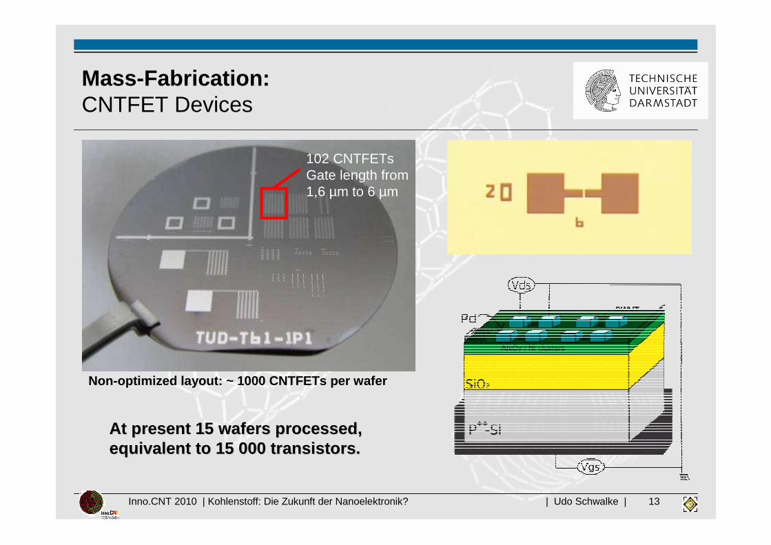
Mass-Fabrication:CNTFET Devices
102 CNTFETsGate length from1,6 µm to 6 µm
At present 15 wafers processed, At present 15 wafers processed, equivalent to 15 000 transistors.equivalent to 15 000 transistors.
Non-optimized layout: ~ 1000 CNTFETs per wafer

Inno.CNT 2010 | Kohlenstoff: Die Zukunft der Nanoelektronik? | Udo Schwalke | 14
Jing Kong, Nathan R. Franklin, ChongwuZhou, Michael G. Chapline, Shu Peng, Kyeongjae Cho, Hongjie Dai
SCIENCE VOL 287 (2000)
Vt-shift: Change in the charging state
Active sensor: Intrinsic amplification
Sensor Applications: CNTFETransistor CNTFESensor

Inno.CNT 2010 | Kohlenstoff: Die Zukunft der Nanoelektronik? | Udo Schwalke | 15
Detection of bio-molecular particles (proteins, vir uses…)Selectivity via functionalization e.g. lipid bi-laye r with viral receptor
Bonding of the virus: change in the charging stateshift in the electrical
characteristicsHigh detection sensitivity Single molecule level
CNTFET CNTFES
e.g. H1N1
Sensor Applications: CNTFES Bio-Sensor

Inno.CNT 2010 | Kohlenstoff: Die Zukunft der Nanoelektronik? | Udo Schwalke | 16
Implantable Sensor System/ Lab-on-a-Chip
Towards Commercial Sensor Applications: Hybrid CNT-CMOS Smart Sensors Systems
• Excellent sensitvity• Ultra-low power • Ultra small• CMOS compatible CMOS compatible
U. Schwalke, L. Rispal, “Fabrication of Ultra-Sensitive Carbon Nanotube Field-Effect Sensors (CNTFES) for Biomedical Applications“, 213th ECS, Phoenix, USA (2008)

Inno.CNT 2010 | Kohlenstoff: Die Zukunft der Nanoelektronik? | Udo Schwalke | 17
M. S. Fuhrer et al., Nano Lett., 755, Vol. 2, No. 7, 2002 J. B. Cui et al. Appl. Phys. Lett., 3260, Vol. 81, N o. 17, 2002M. Radosavljevic et al., Nano Lett., 761, Vol. 2, No. 7, 2002 C. H. Lee et al., Jpn. J. Appl. Phys., 5392, Vol. 4 2 (2003)S. Wang et al. APPLIED PHYSICS LETTERS 87, 133117 2 005M. Y. Zavodchikova et al., phys. stat. sol. (b) 244, No. 11, 4188–4192 (2007)
Wang et al.
•On/off ratios: 100 to 1000
•Logic „1“/“0“: ≤ 100
•Data retention: > 12 days
•Endurance: > 100 cycles
Only few individual memory devices
From CNT-Logic & Sensors to CNT-Memory:Charge-Trapping FET Memories

Inno.CNT 2010 | Kohlenstoff: Die Zukunft der Nanoelektronik? | Udo Schwalke | 18
Basic Memory Functionality: Voltage Programmable Hysteresis
-5 -4 -3 -2 -1 0 1 2 3 4 510-1510-1410-1310-1210-1110-1010-910-810-710-610-5
logical "0"
Ids
(A)
Vgs (s)
logical "1"
memory window
read voltage
Hysteresis: • Charge trapping in
the AlxOy
• or at the AlxOy / SiO2
interface
Performance: • Ion / I off ratio: ~107
• 1 / 0 ratio: ~106
G
S D

Inno.CNT 2010 | Kohlenstoff: Die Zukunft der Nanoelektronik? | Udo Schwalke | 19
Basic Memory Functionality: Data Retention

Inno.CNT 2010 | Kohlenstoff: Die Zukunft der Nanoelektronik? | Udo Schwalke | 20
Basic Memory Functionality: Endurance

Inno.CNT 2010 | Kohlenstoff: Die Zukunft der Nanoelektronik? | Udo Schwalke | 21
Mass-Fabrication: Yield Statistics
Total devices: 252
Oxide thickness: 38 nmGate length: 2 to 6 µm
Total devices: 180
~ 48% Total Yield
Functional Yield Device Yield
Rispal, Schwalke, IEEE Electron Device LettersVol. 29 (12), 1349 (2008)

Inno.CNT 2010 | Kohlenstoff: Die Zukunft der Nanoelektronik? | Udo Schwalke | 22
Outline
Introduction: Motivation for Novel Materials & Devices
Carbon Nanotubes (CNTs): Electronic Properties
1-D: Carbon Nanotube Devices Carbon Nanotube Field-Effect Transistors Carbon Nanotube Sensors Carbon Nanotube Non-Volatile Memory
2-D: Graphene & Graphene Devices
Conclusion

Inno.CNT 2010 | Kohlenstoff: Die Zukunft der Nanoelektronik? | Udo Schwalke | 23
Graphene for Nanoelectronic DevicesGraphene in a “free” state?
Strictly 2D crystal should not exist: (Peierls, Helv. Phys. Acta 7 (1934) 81-83,Peierls, Ann. Inst. H. Poincare 5 (1935) 177-222,Landau, Phys. Z. Sowjet. 11 (1937) 26Mermin, PRL 17 (1966) 1133, Phys. Rev 176 (1968) 250.)
Science, Oct. 2004
armchair edge
zigzag edge
armchair edge
zigzag edge
Geim,Novoselov, Nature Materials 6, 183 (2007)

Inno.CNT 2010 | Kohlenstoff: Die Zukunft der Nanoelektronik? | Udo Schwalke | 24
Favored Industrial Approach:Graphene Devices Top-Down
1µm
1mm
1950 1990 2030
Micro-Electronics
TopTopTopTop----dow
ndow
ndow
ndow
n
Nano-Electronics
1nm
Silicon
Silicon
Silicon
Silicon
SiOSiOSiOSiO2222
AuAuAuAu Graphene
Graphene
Graphene
Graphene
HighHighHighHigh----kkkk
Metal Metal Metal Metal
GateGateGateGate
SourceSourceSourceSource

Inno.CNT 2010 | Kohlenstoff: Die Zukunft der Nanoelektronik? | Udo Schwalke | 25
Graphene Fabrication:Exfoliation Technique
Highly OrientedPyrolytic Graphite

Inno.CNT 2010 | Kohlenstoff: Die Zukunft der Nanoelektronik? | Udo Schwalke | 26
Graphene Fabrication:Exfoliation - Way to Mass-Fabrication?
(high magnification)

Inno.CNT 2010 | Kohlenstoff: Die Zukunft der Nanoelektronik? | Udo Schwalke | 27
Si
AFM Tip
Graphene
Si-Wafer
Catalyst
Oxide
Optical Microscope
CH4 + H2 CVD
Novel Approach to Graphene Fabrication:Catalytic CVD Growth of Graphene
AFM
U. Schwalke, IEEE SCS 2009, Djerba

Inno.CNT 2010 | Kohlenstoff: Die Zukunft der Nanoelektronik? | Udo Schwalke | 28
Conclusion
High Performance Silicon Chips Powered by Carbon-Nanotubes & Graphene
!!!!!!
carbon
carbon
carbon
carbon
carbon
carbon
carbon
carbon
Kohlenstoff: Die Zukunft der Kohlenstoff: Die Zukunft der NanoelektronikNanoelektronik !!!!