k60p120m100sf2 k60 data sheetdatasheet.elcodis.com/pdf2/116/55/1165596/mk60dn512zab10r.pdf ·...
TRANSCRIPT
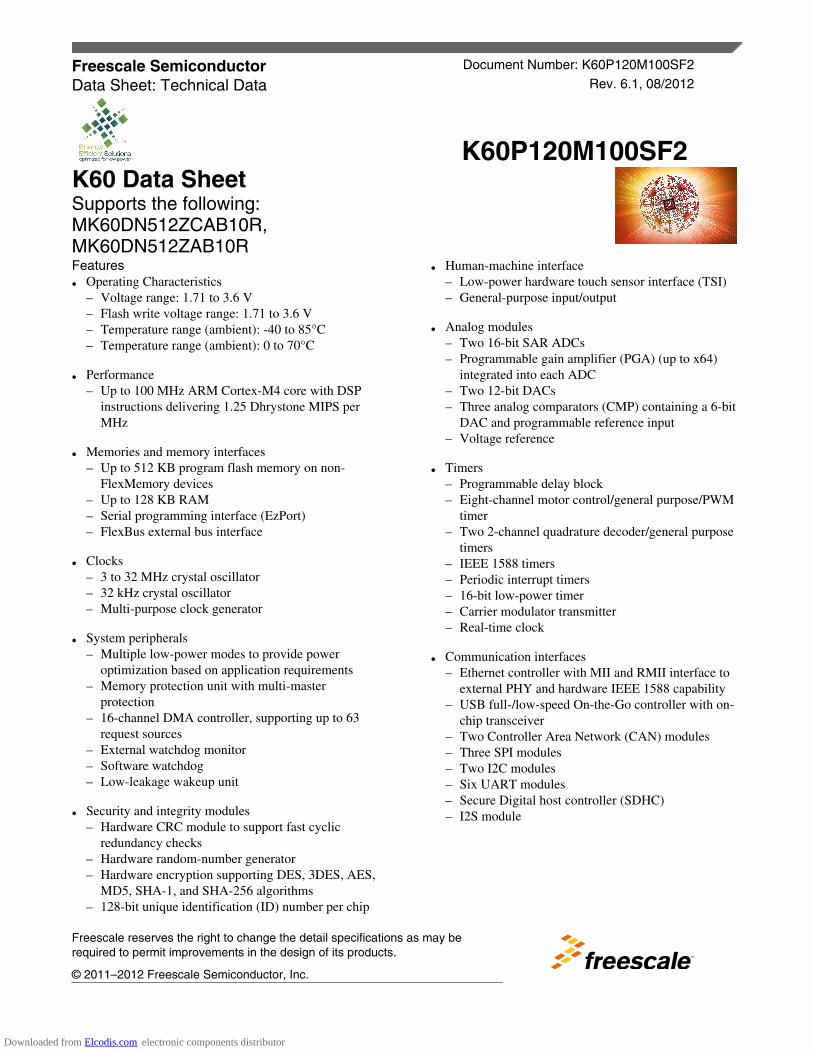
K60P120M100SF2K60 Data SheetSupports the following:MK60DN512ZCAB10R,MK60DN512ZAB10RFeatures• Operating Characteristics
– Voltage range: 1.71 to 3.6 V– Flash write voltage range: 1.71 to 3.6 V– Temperature range (ambient): -40 to 85°C– Temperature range (ambient): 0 to 70°C
• Performance– Up to 100 MHz ARM Cortex-M4 core with DSP
instructions delivering 1.25 Dhrystone MIPS perMHz
• Memories and memory interfaces– Up to 512 KB program flash memory on non-
FlexMemory devices– Up to 128 KB RAM– Serial programming interface (EzPort)– FlexBus external bus interface
• Clocks– 3 to 32 MHz crystal oscillator– 32 kHz crystal oscillator– Multi-purpose clock generator
• System peripherals– Multiple low-power modes to provide power
optimization based on application requirements– Memory protection unit with multi-master
protection– 16-channel DMA controller, supporting up to 63
request sources– External watchdog monitor– Software watchdog– Low-leakage wakeup unit
• Security and integrity modules– Hardware CRC module to support fast cyclic
redundancy checks– Hardware random-number generator– Hardware encryption supporting DES, 3DES, AES,
MD5, SHA-1, and SHA-256 algorithms– 128-bit unique identification (ID) number per chip
• Human-machine interface– Low-power hardware touch sensor interface (TSI)– General-purpose input/output
• Analog modules– Two 16-bit SAR ADCs– Programmable gain amplifier (PGA) (up to x64)
integrated into each ADC– Two 12-bit DACs– Three analog comparators (CMP) containing a 6-bit
DAC and programmable reference input– Voltage reference
• Timers– Programmable delay block– Eight-channel motor control/general purpose/PWM
timer– Two 2-channel quadrature decoder/general purpose
timers– IEEE 1588 timers– Periodic interrupt timers– 16-bit low-power timer– Carrier modulator transmitter– Real-time clock
• Communication interfaces– Ethernet controller with MII and RMII interface to
external PHY and hardware IEEE 1588 capability– USB full-/low-speed On-the-Go controller with on-
chip transceiver– Two Controller Area Network (CAN) modules– Three SPI modules– Two I2C modules– Six UART modules– Secure Digital host controller (SDHC)– I2S module
Freescale Semiconductor Document Number: K60P120M100SF2
Data Sheet: Technical Data Rev. 6.1, 08/2012
Freescale reserves the right to change the detail specifications as may berequired to permit improvements in the design of its products.
© 2011–2012 Freescale Semiconductor, Inc.
Downloaded from Elcodis.com electronic components distributor

K60 Data Sheet Data Sheet, Rev. 6.1, 08/2012.
2 Freescale Semiconductor, Inc.
Downloaded from Elcodis.com electronic components distributor
Table of Contents1 Ordering parts...........................................................................5
1.1 Determining valid orderable parts......................................5
2 Part identification......................................................................5
2.1 Description.........................................................................5
2.2 Format...............................................................................5
2.3 Fields.................................................................................5
2.4 Example............................................................................6
3 Terminology and guidelines......................................................6
3.1 Definition: Operating requirement......................................6
3.2 Definition: Operating behavior...........................................7
3.3 Definition: Attribute............................................................7
3.4 Definition: Rating...............................................................8
3.5 Result of exceeding a rating..............................................8
3.6 Relationship between ratings and operating
requirements......................................................................8
3.7 Guidelines for ratings and operating requirements............9
3.8 Definition: Typical value.....................................................9
3.9 Typical value conditions....................................................10
4 Ratings......................................................................................11
4.1 Thermal handling ratings...................................................11
4.2 Moisture handling ratings..................................................11
4.3 ESD handling ratings.........................................................11
4.4 Voltage and current operating ratings...............................11
5 General.....................................................................................12
5.1 AC electrical characteristics..............................................12
5.2 Nonswitching electrical specifications...............................12
5.2.1 Voltage and current operating requirements......13
5.2.2 LVD and POR operating requirements...............14
5.2.3 Voltage and current operating behaviors............14
5.2.4 Power mode transition operating behaviors.......15
5.2.5 Power consumption operating behaviors............16
5.2.6 EMC radiated emissions operating behaviors....19
5.2.7 Designing with radiated emissions in mind.........20
5.2.8 Capacitance attributes........................................20
5.3 Switching specifications.....................................................20
5.3.1 Device clock specifications.................................20
5.3.2 General switching specifications.........................20
5.4 Thermal specifications.......................................................21
5.4.1 Thermal operating requirements.........................21
5.4.2 Thermal attributes...............................................22
6 Peripheral operating requirements and behaviors....................23
6.1 Core modules....................................................................23
6.1.1 Debug trace timing specifications.......................23
6.1.2 JTAG electricals..................................................23
6.2 System modules................................................................26
6.3 Clock modules...................................................................26
6.3.1 MCG specifications.............................................26
6.3.2 Oscillator electrical specifications.......................28
6.3.3 32 kHz Oscillator Electrical Characteristics........31
6.4 Memories and memory interfaces.....................................31
6.4.1 Flash electrical specifications.............................31
6.4.2 EzPort Switching Specifications.........................33
6.4.3 Flexbus Switching Specifications........................34
6.5 Security and integrity modules..........................................37
6.6 Analog...............................................................................37
6.6.1 ADC electrical specifications..............................37
6.6.2 CMP and 6-bit DAC electrical specifications......45
6.6.3 12-bit DAC electrical characteristics...................47
6.6.4 Voltage reference electrical specifications..........50
6.7 Timers................................................................................51
6.8 Communication interfaces.................................................51
6.8.1 Ethernet switching specifications........................52
6.8.2 USB electrical specifications...............................53
6.8.3 USB DCD electrical specifications......................53
6.8.4 USB VREG electrical specifications...................54
6.8.5 CAN switching specifications..............................54
6.8.6 DSPI switching specifications (limited voltage
range).................................................................55
6.8.7 DSPI switching specifications (full voltage
range).................................................................56
6.8.8 I2C switching specifications................................58
6.8.9 UART switching specifications............................58
6.8.10 SDHC specifications...........................................58
6.8.11 I2S switching specifications................................59
6.9 Human-machine interfaces (HMI)......................................61
6.9.1 TSI electrical specifications................................61
7 Dimensions...............................................................................62
7.1 Obtaining package dimensions.........................................62
8 Pinout........................................................................................62
8.1 K60 Signal Multiplexing and Pin Assignments..................62
K60 Data Sheet Data Sheet, Rev. 6.1, 08/2012.
Freescale Semiconductor, Inc. 3
Downloaded from Elcodis.com electronic components distributor
8.2 K60 Pinouts.......................................................................67 9 Revision History........................................................................68
K60 Data Sheet Data Sheet, Rev. 6.1, 08/2012.
4 Freescale Semiconductor, Inc.
Downloaded from Elcodis.com electronic components distributor
1 Ordering parts
1.1 Determining valid orderable parts
Valid orderable part numbers are provided on the web. To determine the orderable partnumbers for this device, go to www.freescale.com and perform a part number search forthe following device numbers: PK60 and MK60.
2 Part identification
2.1 Description
Part numbers for the chip have fields that identify the specific part. You can use thevalues of these fields to determine the specific part you have received.
2.2 Format
Part numbers for this device have the following format:
Q K## A M FFF R T PP CC N
2.3 Fields
This table lists the possible values for each field in the part number (not all combinationsare valid):
Field Description Values
Q Qualification status • M = Fully qualified, general market flow• P = Prequalification
K## Kinetis family • K60
A Key attribute • D = Cortex-M4 w/ DSP• F = Cortex-M4 w/ DSP and FPU
M Flash memory type • N = Program flash only• X = Program flash and FlexMemory
Table continues on the next page...
Ordering parts
K60 Data Sheet Data Sheet, Rev. 6.1, 08/2012.
Freescale Semiconductor, Inc. 5
Downloaded from Elcodis.com electronic components distributor
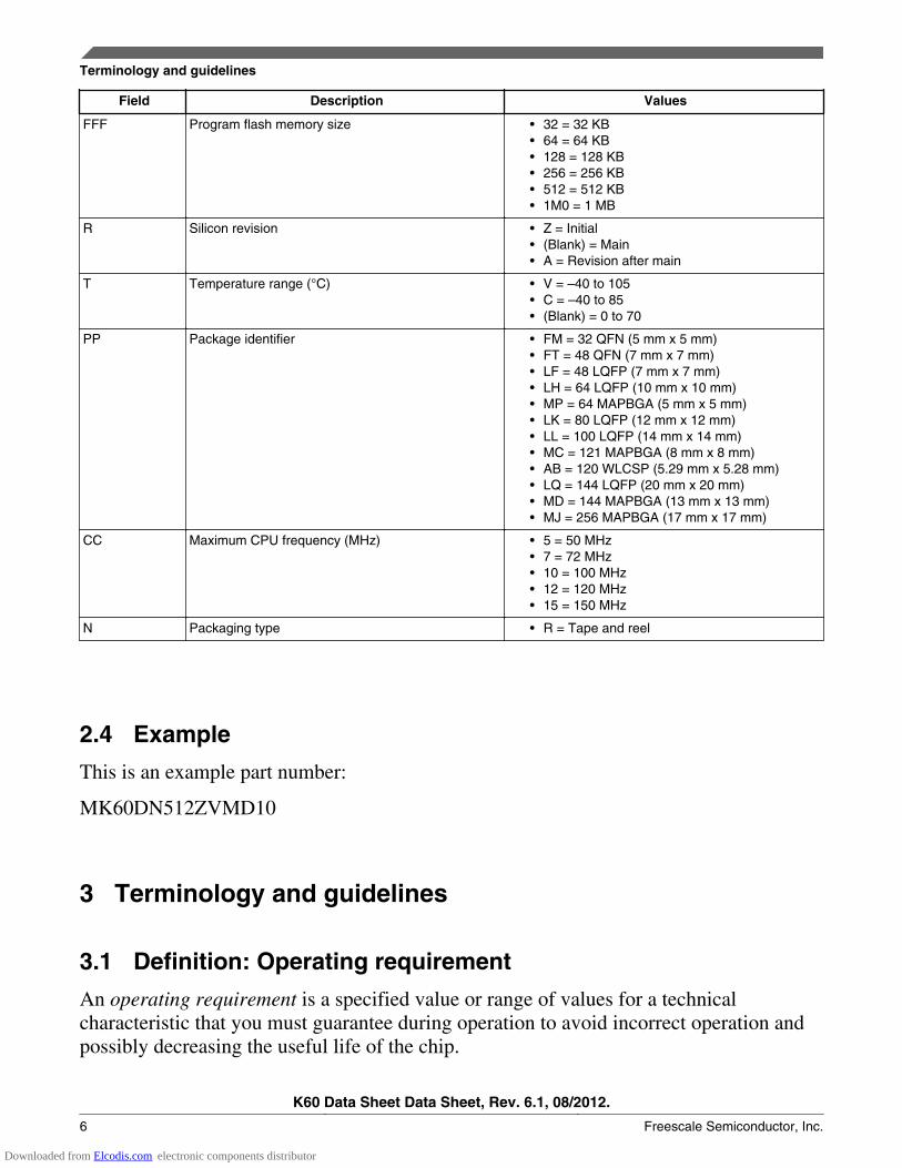
Field Description Values
FFF Program flash memory size • 32 = 32 KB• 64 = 64 KB• 128 = 128 KB• 256 = 256 KB• 512 = 512 KB• 1M0 = 1 MB
R Silicon revision • Z = Initial• (Blank) = Main• A = Revision after main
T Temperature range (°C) • V = –40 to 105• C = –40 to 85• (Blank) = 0 to 70
PP Package identifier • FM = 32 QFN (5 mm x 5 mm)• FT = 48 QFN (7 mm x 7 mm)• LF = 48 LQFP (7 mm x 7 mm)• LH = 64 LQFP (10 mm x 10 mm)• MP = 64 MAPBGA (5 mm x 5 mm)• LK = 80 LQFP (12 mm x 12 mm)• LL = 100 LQFP (14 mm x 14 mm)• MC = 121 MAPBGA (8 mm x 8 mm)• AB = 120 WLCSP (5.29 mm x 5.28 mm)• LQ = 144 LQFP (20 mm x 20 mm)• MD = 144 MAPBGA (13 mm x 13 mm)• MJ = 256 MAPBGA (17 mm x 17 mm)
CC Maximum CPU frequency (MHz) • 5 = 50 MHz• 7 = 72 MHz• 10 = 100 MHz• 12 = 120 MHz• 15 = 150 MHz
N Packaging type • R = Tape and reel
2.4 Example
This is an example part number:
MK60DN512ZVMD10
3 Terminology and guidelines
3.1 Definition: Operating requirement
An operating requirement is a specified value or range of values for a technicalcharacteristic that you must guarantee during operation to avoid incorrect operation andpossibly decreasing the useful life of the chip.
Terminology and guidelines
K60 Data Sheet Data Sheet, Rev. 6.1, 08/2012.
6 Freescale Semiconductor, Inc.
Downloaded from Elcodis.com electronic components distributor
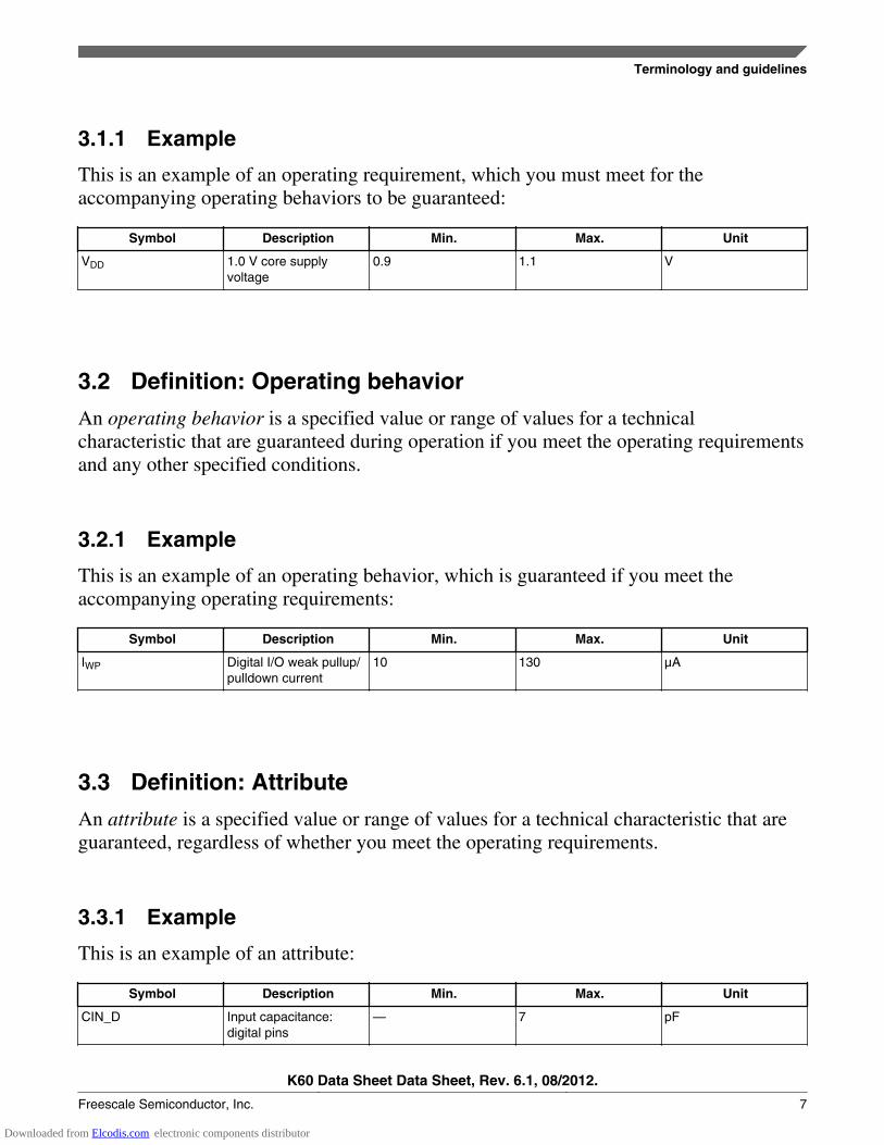
3.1.1 Example
This is an example of an operating requirement, which you must meet for theaccompanying operating behaviors to be guaranteed:
Symbol Description Min. Max. Unit
VDD 1.0 V core supplyvoltage
0.9 1.1 V
3.2 Definition: Operating behavior
An operating behavior is a specified value or range of values for a technicalcharacteristic that are guaranteed during operation if you meet the operating requirementsand any other specified conditions.
3.2.1 Example
This is an example of an operating behavior, which is guaranteed if you meet theaccompanying operating requirements:
Symbol Description Min. Max. Unit
IWP Digital I/O weak pullup/pulldown current
10 130 µA
3.3 Definition: Attribute
An attribute is a specified value or range of values for a technical characteristic that areguaranteed, regardless of whether you meet the operating requirements.
3.3.1 Example
This is an example of an attribute:
Symbol Description Min. Max. Unit
CIN_D Input capacitance:digital pins
— 7 pF
Terminology and guidelines
K60 Data Sheet Data Sheet, Rev. 6.1, 08/2012.
Freescale Semiconductor, Inc. 7
Downloaded from Elcodis.com electronic components distributor
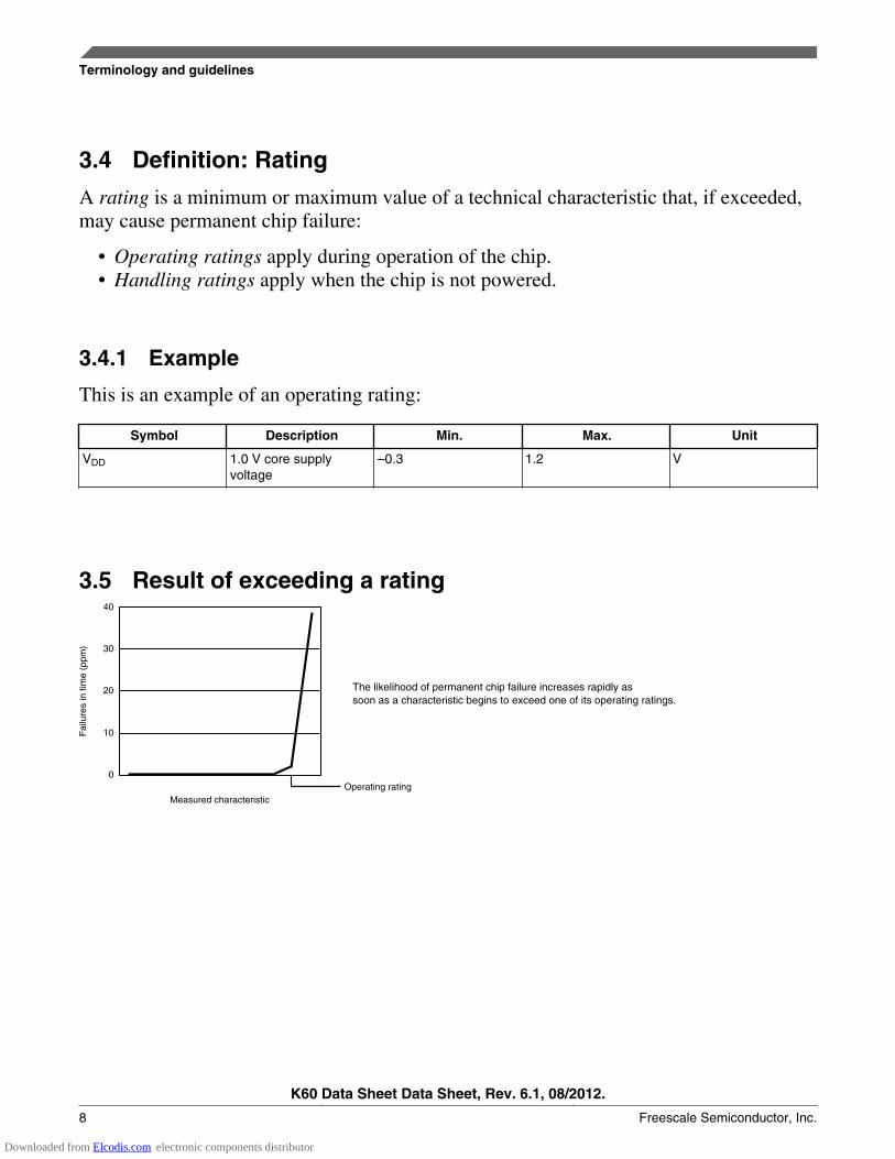
3.4 Definition: Rating
A rating is a minimum or maximum value of a technical characteristic that, if exceeded,may cause permanent chip failure:
• Operating ratings apply during operation of the chip.• Handling ratings apply when the chip is not powered.
3.4.1 Example
This is an example of an operating rating:
Symbol Description Min. Max. Unit
VDD 1.0 V core supplyvoltage
–0.3 1.2 V
3.5 Result of exceeding a rating40
30
20
10
0
Measured characteristicOperating rating
Fai
lure
s in
tim
e (p
pm)
The likelihood of permanent chip failure increases rapidly as soon as a characteristic begins to exceed one of its operating ratings.
Terminology and guidelines
K60 Data Sheet Data Sheet, Rev. 6.1, 08/2012.
8 Freescale Semiconductor, Inc.
Downloaded from Elcodis.com electronic components distributor
3.6 Relationship between ratings and operating requirements
–∞
- No permanent failure- Correct operation
Normal operating rangeFatal range
Expected permanent failure
Fatal range
Expected permanent failure
∞
Operating rating (m
ax.)
Operating requirement (m
ax.)
Operating requirement (m
in.)
Operating rating (m
in.)
Operating (power on)
Degraded operating range Degraded operating range
–∞
No permanent failure
Handling rangeFatal range
Expected permanent failure
Fatal range
Expected permanent failure
∞
Handling rating (m
ax.)
Handling rating (m
in.)
Handling (power off)
- No permanent failure- Possible decreased life- Possible incorrect operation
- No permanent failure- Possible decreased life- Possible incorrect operation
3.7 Guidelines for ratings and operating requirements
Follow these guidelines for ratings and operating requirements:
• Never exceed any of the chip’s ratings.• During normal operation, don’t exceed any of the chip’s operating requirements.• If you must exceed an operating requirement at times other than during normal
operation (for example, during power sequencing), limit the duration as much aspossible.
3.8 Definition: Typical valueA typical value is a specified value for a technical characteristic that:
• Lies within the range of values specified by the operating behavior• Given the typical manufacturing process, is representative of that characteristic
during operation when you meet the typical-value conditions or other specifiedconditions
Typical values are provided as design guidelines and are neither tested nor guaranteed.
Terminology and guidelines
K60 Data Sheet Data Sheet, Rev. 6.1, 08/2012.
Freescale Semiconductor, Inc. 9
Downloaded from Elcodis.com electronic components distributor
3.8.1 Example 1
This is an example of an operating behavior that includes a typical value:
Symbol Description Min. Typ. Max. Unit
IWP Digital I/O weakpullup/pulldowncurrent
10 70 130 µA
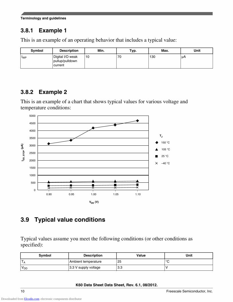
3.8.2 Example 2
This is an example of a chart that shows typical values for various voltage andtemperature conditions:
0.90 0.95 1.00 1.05 1.10
0
500
1000
1500
2000
2500
3000
3500
4000
4500
5000
150 °C
105 °C
25 °C
–40 °C
VDD (V)
I(μ
A)
DD
_ST
OP
TJ
3.9 Typical value conditions
Typical values assume you meet the following conditions (or other conditions asspecified):
Symbol Description Value Unit
TA Ambient temperature 25 °C
VDD 3.3 V supply voltage 3.3 V
Terminology and guidelines
K60 Data Sheet Data Sheet, Rev. 6.1, 08/2012.
10 Freescale Semiconductor, Inc.
Downloaded from Elcodis.com electronic components distributor
4 Ratings
4.1 Thermal handling ratings
Symbol Description Min. Max. Unit Notes
TSTG Storage temperature –55 150 °C 1
TSDR Solder temperature, lead-free — 260 °C 2
Solder temperature, leaded — 245
1. Determined according to JEDEC Standard JESD22-A103, High Temperature Storage Life.2. Determined according to IPC/JEDEC Standard J-STD-020, Moisture/Reflow Sensitivity Classification for Nonhermetic
Solid State Surface Mount Devices.
4.2 Moisture handling ratings
Symbol Description Min. Max. Unit Notes
MSL Moisture sensitivity level — 3 — 1
1. Determined according to IPC/JEDEC Standard J-STD-020, Moisture/Reflow Sensitivity Classification for NonhermeticSolid State Surface Mount Devices.
4.3 ESD handling ratings
Symbol Description Min. Max. Unit Notes
VHBM Electrostatic discharge voltage, human body model -2000 +2000 V 1
VCDM Electrostatic discharge voltage, charged-device model -500 +500 V 2
ILAT Latch-up current at ambient temperature of 105°C -100 +100 mA
1. Determined according to JEDEC Standard JESD22-A114, Electrostatic Discharge (ESD) Sensitivity Testing Human BodyModel (HBM).
2. Determined according to JEDEC Standard JESD22-C101, Field-Induced Charged-Device Model Test Method forElectrostatic-Discharge-Withstand Thresholds of Microelectronic Components.
4.4 Voltage and current operating ratings
Ratings
K60 Data Sheet Data Sheet, Rev. 6.1, 08/2012.
Freescale Semiconductor, Inc. 11
Downloaded from Elcodis.com electronic components distributor
Symbol Description Min. Max. Unit
VDD Digital supply voltage –0.3 3.8 V
IDD Digital supply current — 185 mA
VDIO Digital input voltage (except RESET, EXTAL, and XTAL) –0.3 5.5 V
VAIO Analog1, RESET, EXTAL, and XTAL input voltage –0.3 VDD + 0.3 V
ID Maximum current single pin limit (applies to all port pins) –25 25 mA
VDDA Analog supply voltage VDD – 0.3 VDD + 0.3 V
VUSB_DP USB_DP input voltage –0.3 3.63 V
VUSB_DM USB_DM input voltage –0.3 3.63 V
VREGIN USB regulator input –0.3 6.0 V
VBAT RTC battery supply voltage –0.3 3.8 V
1. Analog pins are defined as pins that do not have an associated general purpose I/O port function.
5 General
5.1 AC electrical characteristics
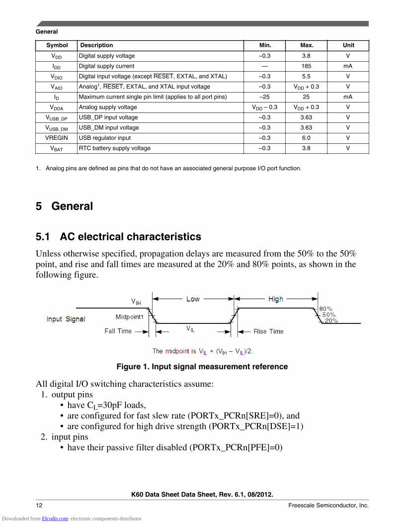
Unless otherwise specified, propagation delays are measured from the 50% to the 50%point, and rise and fall times are measured at the 20% and 80% points, as shown in thefollowing figure.
Figure 1. Input signal measurement reference
All digital I/O switching characteristics assume:1. output pins
• have CL=30pF loads,• are configured for fast slew rate (PORTx_PCRn[SRE]=0), and• are configured for high drive strength (PORTx_PCRn[DSE]=1)
2. input pins• have their passive filter disabled (PORTx_PCRn[PFE]=0)
General
K60 Data Sheet Data Sheet, Rev. 6.1, 08/2012.
12 Freescale Semiconductor, Inc.
Downloaded from Elcodis.com electronic components distributor
5.2 Nonswitching electrical specifications
5.2.1 Voltage and current operating requirementsTable 1. Voltage and current operating requirements
Symbol Description Min. Max. Unit Notes
VDD Supply voltage 1.71 3.6 V
VDDA Analog supply voltage 1.71 3.6 V
VDD – VDDA VDD-to-VDDA differential voltage –0.1 0.1 V
VSS – VSSA VSS-to-VSSA differential voltage –0.1 0.1 V
VBAT RTC battery supply voltage 1.71 3.6 V
VIH Input high voltage
• 2.7 V ≤ VDD ≤ 3.6 V
• 1.7 V ≤ VDD ≤ 2.7 V
0.7 × VDD
0.75 × VDD
—
—
V
V
VIL Input low voltage
• 2.7 V ≤ VDD ≤ 3.6 V
• 1.7 V ≤ VDD ≤ 2.7 V
—
—
0.35 × VDD
0.3 × VDD
V
V
VHYS Input hysteresis 0.06 × VDD — V
IICDIO Digital pin negative DC injection current — single pin
• VIN < VSS-0.3V-5 — mA
1
IICAIO Analog2, EXTAL, and XTAL pin DC injection current —single pin
• VIN < VSS-0.3V (Negative current injection)
• VIN > VDD+0.3V (Positive current injection)
-5
—
—
+5
mA
3
IICcont Contiguous pin DC injection current —regional limit,includes sum of negative injection currents or sum ofpositive injection currents of 16 contiguous pins
• Negative current injection
• Positive current injection
-25
—
—
+25
mA
VRAM VDD voltage required to retain RAM 1.2 — V
VRFVBAT VBAT voltage required to retain the VBAT register file VPOR_VBAT — V
1. All 5 V tolerant digital I/O pins are internally clamped to VSS through a ESD protection diode. There is no diode connectionto VDD. If VIN greater than VDIO_MIN (=VSS-0.3V) is observed, then there is no need to provide current limiting resistors atthe pads. If this limit cannot be observed then a current limiting resistor is required. The negative DC injection currentlimiting resistor is calculated as R=(VDIO_MIN-VIN)/|IIC|.
2. Analog pins are defined as pins that do not have an associated general purpose I/O port function.3. All analog pins are internally clamped to VSS and VDD through ESD protection diodes. If VIN is greater than VAIO_MIN
(=VSS-0.3V) and VIN is less than VAIO_MAX(=VDD+0.3V) is observed, then there is no need to provide current limitingresistors at the pads. If these limits cannot be observed then a current limiting resistor is required. The negative DCinjection current limiting resistor is calculated as R=(VAIO_MIN-VIN)/|IIC|. The positive injection current limiting resistor iscalcualted as R=(VIN-VAIO_MAX)/|IIC|. Select the larger of these two calculated resistances.
General
K60 Data Sheet Data Sheet, Rev. 6.1, 08/2012.
Freescale Semiconductor, Inc. 13
Downloaded from Elcodis.com electronic components distributor
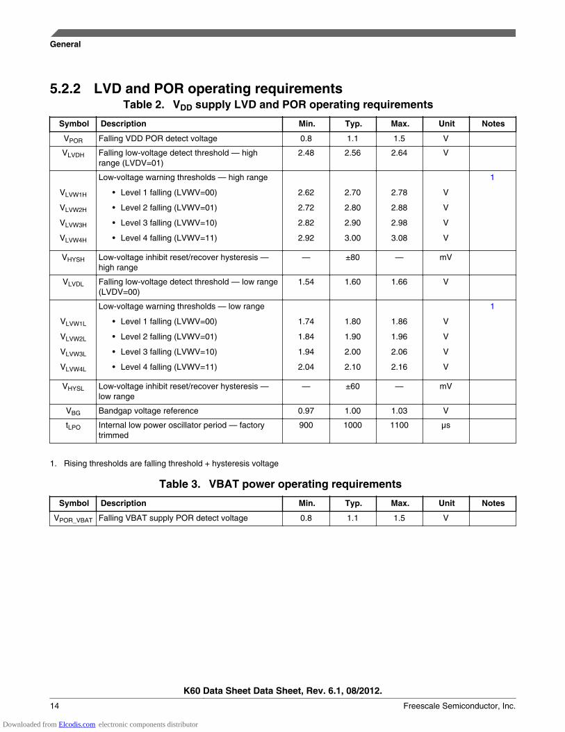
5.2.2 LVD and POR operating requirementsTable 2. VDD supply LVD and POR operating requirements
Symbol Description Min. Typ. Max. Unit Notes
VPOR Falling VDD POR detect voltage 0.8 1.1 1.5 V
VLVDH Falling low-voltage detect threshold — highrange (LVDV=01)
2.48 2.56 2.64 V
VLVW1H
VLVW2H
VLVW3H
VLVW4H
Low-voltage warning thresholds — high range
• Level 1 falling (LVWV=00)
• Level 2 falling (LVWV=01)
• Level 3 falling (LVWV=10)
• Level 4 falling (LVWV=11)
2.62
2.72
2.82
2.92
2.70
2.80
2.90
3.00
2.78
2.88
2.98
3.08
V
V
V
V
1
VHYSH Low-voltage inhibit reset/recover hysteresis —high range
— ±80 — mV
VLVDL Falling low-voltage detect threshold — low range(LVDV=00)
1.54 1.60 1.66 V
VLVW1L
VLVW2L
VLVW3L
VLVW4L
Low-voltage warning thresholds — low range
• Level 1 falling (LVWV=00)
• Level 2 falling (LVWV=01)
• Level 3 falling (LVWV=10)
• Level 4 falling (LVWV=11)
1.74
1.84
1.94
2.04
1.80
1.90
2.00
2.10
1.86
1.96
2.06
2.16
V
V
V
V
1
VHYSL Low-voltage inhibit reset/recover hysteresis —low range
— ±60 — mV
VBG Bandgap voltage reference 0.97 1.00 1.03 V
tLPO Internal low power oscillator period — factorytrimmed
900 1000 1100 μs
1. Rising thresholds are falling threshold + hysteresis voltage
Table 3. VBAT power operating requirements
Symbol Description Min. Typ. Max. Unit Notes
VPOR_VBAT Falling VBAT supply POR detect voltage 0.8 1.1 1.5 V
General
K60 Data Sheet Data Sheet, Rev. 6.1, 08/2012.
14 Freescale Semiconductor, Inc.
Downloaded from Elcodis.com electronic components distributor
5.2.3 Voltage and current operating behaviorsTable 4. Voltage and current operating behaviors
Symbol Description Min. Max. Unit Notes
VOH Output high voltage — high drive strength
• 2.7 V ≤ VDD ≤ 3.6 V, IOH = -9mA
• 1.71 V ≤ VDD ≤ 2.7 V, IOH = -3mA
VDD – 0.5
VDD – 0.5
—
—
V
V
Output high voltage — low drive strength
• 2.7 V ≤ VDD ≤ 3.6 V, IOH = -2mA
• 1.71 V ≤ VDD ≤ 2.7 V, IOH = -0.6mA
VDD – 0.5
VDD – 0.5
—
—
V
V
IOHT Output high current total for all ports — 100 mA
VOL Output low voltage — high drive strength
• 2.7 V ≤ VDD ≤ 3.6 V, IOL = 9mA
• 1.71 V ≤ VDD ≤ 2.7 V, IOL = 3mA
—
—
0.5
0.5
V
V
Output low voltage — low drive strength
• 2.7 V ≤ VDD ≤ 3.6 V, IOL = 2mA
• 1.71 V ≤ VDD ≤ 2.7 V, IOL = 0.6mA
—
—
0.5
0.5
V
V
IOLT Output low current total for all ports — 100 mA
IIN Input leakage current (per pin) for full temperaturerange
— 1 μA 1
IIN Input leakage current (per pin) at 25°C — 0.025 μA 1
IOZ Hi-Z (off-state) leakage current (per pin) — 1 μA
RPU Internal pullup resistors 20 50 kΩ 2
RPD Internal pulldown resistors 20 50 kΩ 3
1. Measured at VDD=3.6V2. Measured at VDD supply voltage = VDD min and Vinput = VSS3. Measured at VDD supply voltage = VDD min and Vinput = VDD
5.2.4 Power mode transition operating behaviors
All specifications except tPOR, and VLLSx→RUN recovery times in the following tableassume this clock configuration:
• CPU and system clocks = 100 MHz• Bus clock = 50 MHz• FlexBus clock = 50 MHz• Flash clock = 25 MHz
General
K60 Data Sheet Data Sheet, Rev. 6.1, 08/2012.
Freescale Semiconductor, Inc. 15
Downloaded from Elcodis.com electronic components distributor
Table 5. Power mode transition operating behaviors
Symbol Description Min. Max. Unit Notes
tPOR After a POR event, amount of time from the point VDDreaches 1.71 V to execution of the first instructionacross the operating temperature range of the chip.
— 300 μs 1
• VLLS1 → RUN— 112 μs
• VLLS2 → RUN— 74 μs
• VLLS3 → RUN— 73 μs
• LLS → RUN— 5.9 μs
• VLPS → RUN— 5.8 μs
• STOP → RUN— 4.2 μs
1. Normal boot (FTFL_OPT[LPBOOT]=1)
5.2.5 Power consumption operating behaviorsTable 6. Power consumption operating behaviors
Symbol Description Min. Typ. Max. Unit Notes
IDDA Analog supply current — — See note mA 1
IDD_RUN Run mode current — all peripheral clocksdisabled, code executing from flash
• @ 1.8V
• @ 3.0V
—
—
45
47
70
72
mA
mA
2
IDD_RUN Run mode current — all peripheral clocksenabled, code executing from flash
• @ 1.8V
• @ 3.0V
• @ 25°C
• @ 80°C
• @ 95°C
—
—
—
—
61
63
72
72
85
71
77
81
mA
mA
mA
mA
3, 4
IDD_WAIT Wait mode high frequency current at 3.0 V — allperipheral clocks disabled
— 35 — mA 2
IDD_WAIT Wait mode reduced frequency current at 3.0 V —all peripheral clocks disabled
— 15 — mA 5
IDD_VLPR Very-low-power run mode current at 3.0 V — allperipheral clocks disabled
— N/A — mA 6
IDD_VLPR Very-low-power run mode current at 3.0 V — allperipheral clocks enabled
— N/A — mA 7
Table continues on the next page...
General
K60 Data Sheet Data Sheet, Rev. 6.1, 08/2012.
16 Freescale Semiconductor, Inc.
Downloaded from Elcodis.com electronic components distributor
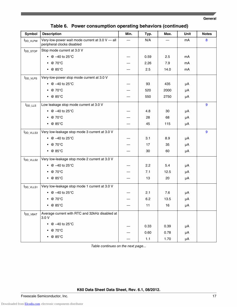
Table 6. Power consumption operating behaviors (continued)
Symbol Description Min. Typ. Max. Unit Notes
IDD_VLPW Very-low-power wait mode current at 3.0 V — allperipheral clocks disabled
— N/A — mA 8
IDD_STOP Stop mode current at 3.0 V
• @ –40 to 25°C
• @ 70°C
• @ 85°C
—
—
—
0.59
2.26
2.5
2.5
7.9
14.0
mA
mA
mA
IDD_VLPS Very-low-power stop mode current at 3.0 V
• @ –40 to 25°C
• @ 70°C
• @ 85°C
—
—
—
93
520
550
435
2000
2750
μA
μA
μA
IDD_LLS Low leakage stop mode current at 3.0 V
• @ –40 to 25°C
• @ 70°C
• @ 85°C
—
—
—
4.8
28
45
30
68
115
μA
μA
μA
9
IDD_VLLS3 Very low-leakage stop mode 3 current at 3.0 V
• @ –40 to 25°C
• @ 70°C
• @ 85°C
—
—
—
3.1
17
30
8.9
35
60
μA
μA
μA
9
IDD_VLLS2 Very low-leakage stop mode 2 current at 3.0 V
• @ –40 to 25°C
• @ 70°C
• @ 85°C
—
—
—
2.2
7.1
13
5.4
12.5
20
μA
μA
μA
IDD_VLLS1 Very low-leakage stop mode 1 current at 3.0 V
• @ –40 to 25°C
• @ 70°C
• @ 85°C
—
—
—
2.1
6.2
11
7.6
13.5
16
μA
μA
μA
IDD_VBAT Average current with RTC and 32kHz disabled at3.0 V
• @ –40 to 25°C
• @ 70°C
• @ 85°C
—
—
—
0.33
0.60
1.1
0.39
0.78
1.70
μA
μA
μA
Table continues on the next page...
General
K60 Data Sheet Data Sheet, Rev. 6.1, 08/2012.
Freescale Semiconductor, Inc. 17
Downloaded from Elcodis.com electronic components distributor
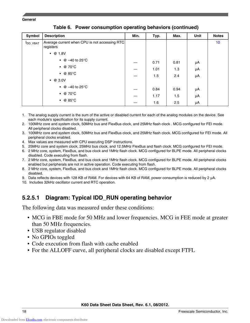
Table 6. Power consumption operating behaviors (continued)
Symbol Description Min. Typ. Max. Unit Notes
IDD_VBAT Average current when CPU is not accessing RTCregisters
• @ 1.8V
• @ –40 to 25°C
• @ 70°C
• @ 85°C
• @ 3.0V
• @ –40 to 25°C
• @ 70°C
• @ 85°C
—
—
—
—
—
—
0.71
1.01
1.5
0.84
1.17
1.6
0.81
1.3
2.4
0.94
1.5
2.5
μA
μA
μA
μA
μA
μA
10
1. The analog supply current is the sum of the active or disabled current for each of the analog modules on the device. Seeeach module's specification for its supply current.
2. 100MHz core and system clock, 50MHz bus and FlexBus clock, and 25MHz flash clock . MCG configured for FEI mode.All peripheral clocks disabled.
3. 100MHz core and system clock, 50MHz bus and FlexBus clock, and 25MHz flash clock. MCG configured for FEI mode. Allperipheral clocks enabled.
4. Max values are measured with CPU executing DSP instructions.5. 25MHz core and system clock, 25MHz bus clock, and 12.5MHz FlexBus and flash clock. MCG configured for FEI mode.6. 2 MHz core, system, FlexBus, and bus clock and 1MHz flash clock. MCG configured for BLPE mode. All peripheral clocks
disabled. Code executing from flash.7. 2 MHz core, system, FlexBus, and bus clock and 1MHz flash clock. MCG configured for BLPE mode. All peripheral clocks
enabled but peripherals are not in active operation. Code executing from flash.8. 2 MHz core, system, FlexBus, and bus clock and 1MHz flash clock. MCG configured for BLPE mode. All peripheral clocks
disabled.9. Data reflects devices with 128 KB of RAM. For devices with 64 KB of RAM, power consumption is reduced by 2 μA.10. Includes 32kHz oscillator current and RTC operation.
5.2.5.1 Diagram: Typical IDD_RUN operating behavior
The following data was measured under these conditions:
• MCG in FBE mode for 50 MHz and lower frequencies. MCG in FEE mode at greaterthan 50 MHz frequencies.
• USB regulator disabled• No GPIOs toggled• Code execution from flash with cache enabled• For the ALLOFF curve, all peripheral clocks are disabled except FTFL
General
K60 Data Sheet Data Sheet, Rev. 6.1, 08/2012.
18 Freescale Semiconductor, Inc.
Downloaded from Elcodis.com electronic components distributor
Figure 2. Run mode supply current vs. core frequency
5.2.6 EMC radiated emissions operating behaviorsTable 7. EMC radiated emissions operating behaviors for 144LQFP
Symbol Description Frequencyband (MHz)
Typ. Unit Notes
VRE1 Radiated emissions voltage, band 1 0.15–50 23 dBμV 1 , 2
VRE2 Radiated emissions voltage, band 2 50–150 27 dBμV
VRE3 Radiated emissions voltage, band 3 150–500 28 dBμV
VRE4 Radiated emissions voltage, band 4 500–1000 14 dBμV
VRE_IEC IEC level 0.15–1000 K — 2, 3
1. Determined according to IEC Standard 61967-1, Integrated Circuits - Measurement of Electromagnetic Emissions, 150kHz to 1 GHz Part 1: General Conditions and Definitions and IEC Standard 61967-2, Integrated Circuits - Measurement ofElectromagnetic Emissions, 150 kHz to 1 GHz Part 2: Measurement of Radiated Emissions—TEM Cell and WidebandTEM Cell Method. Measurements were made while the microcontroller was running basic application code. The reportedemission level is the value of the maximum measured emission, rounded up to the next whole number, from among themeasured orientations in each frequency range.
2. VDD = 3.3 V, TA = 25 °C, fOSC = 12 MHz (crystal), fSYS = 96 MHz, fBUS = 48MHz
General
K60 Data Sheet Data Sheet, Rev. 6.1, 08/2012.
Freescale Semiconductor, Inc. 19
Downloaded from Elcodis.com electronic components distributor
3. Specified according to Annex D of IEC Standard 61967-2, Measurement of Radiated Emissions—TEM Cell and WidebandTEM Cell Method
5.2.7 Designing with radiated emissions in mind
To find application notes that provide guidance on designing your system to minimizeinterference from radiated emissions:
1. Go to www.freescale.com.2. Perform a keyword search for “EMC design.”
5.2.8 Capacitance attributesTable 8. Capacitance attributes
Symbol Description Min. Max. Unit
CIN_A Input capacitance: analog pins — 7 pF
CIN_D Input capacitance: digital pins — 7 pF
5.3 Switching specifications
5.3.1 Device clock specificationsTable 9. Device clock specifications
Symbol Description Min. Max. Unit Notes
Normal run mode
fSYS System and core clock — 100 MHz
fSYS_USB System and core clock when Full Speed USB inoperation
20 — MHz
fENET System and core clock when ethernet in operation
• 10 Mbps• 100 Mbps
5
50
—
—
MHz
fBUS Bus clock — 50 MHz
FB_CLK FlexBus clock — 50 MHz
fFLASH Flash clock — 25 MHz
fLPTMR LPTMR clock — 25 MHz
General
K60 Data Sheet Data Sheet, Rev. 6.1, 08/2012.
20 Freescale Semiconductor, Inc.
Downloaded from Elcodis.com electronic components distributor
5.3.2 General switching specifications
These general purpose specifications apply to all signals configured for GPIO, UART,CAN, CMT, IEEE 1588 timer, and I2C signals.
Table 10. General switching specifications
Symbol Description Min. Max. Unit Notes
GPIO pin interrupt pulse width (digital glitch filterdisabled) — Synchronous path
1.5 — Bus clockcycles
1, 2
GPIO pin interrupt pulse width (digital glitch filterdisabled, analog filter enabled) — Asynchronous path
100 — ns 3
GPIO pin interrupt pulse width (digital glitch filterdisabled, analog filter disabled) — Asynchronous path
16 — ns 3
External reset pulse width (digital glitch filter disabled) 100 — ns 3
Mode select (EZP_CS) hold time after resetdeassertion
2 — Bus clockcycles
Port rise and fall time (high drive strength)
• Slew disabled
• 1.71 ≤ VDD ≤ 2.7V
• 2.7 ≤ VDD ≤ 3.6V
• Slew enabled
• 1.71 ≤ VDD ≤ 2.7V
• 2.7 ≤ VDD ≤ 3.6V
—
—
—
—
12
6
36
24
ns
ns
ns
ns
4
Port rise and fall time (low drive strength)
• Slew disabled
• 1.71 ≤ VDD ≤ 2.7V
• 2.7 ≤ VDD ≤ 3.6V
• Slew enabled
• 1.71 ≤ VDD ≤ 2.7V
• 2.7 ≤ VDD ≤ 3.6V
—
—
—
—
12
6
36
24
ns
ns
ns
ns
5
1. This is the minimum pulse width that is guaranteed to pass through the pin synchronization circuitry. Shorter pulses may ormay not be recognized. In Stop, VLPS, LLS, and VLLSx modes, the synchronizer is bypassed so shorter pulses can berecognized in that case.
2. The greater synchronous and asynchronous timing must be met.3. This is the minimum pulse width that is guaranteed to be recognized as a pin interrupt request in Stop, VLPS, LLS, and
VLLSx modes.4. 75pF load5. 15pF load
5.4 Thermal specifications
General
K60 Data Sheet Data Sheet, Rev. 6.1, 08/2012.
Freescale Semiconductor, Inc. 21
Downloaded from Elcodis.com electronic components distributor
5.4.1 Thermal operating requirementsTable 11. Thermal operating requirements
Symbol Description Min. Max. Unit
MK60DN512ZCAB10R
TJ Die junction temperature –40 95 °C
TA Ambient temperature –40 85 °C
MK60DN512ZAB10R
TJ Die junction temperature 0 80 °C
TA Ambient temperature 0 70 °C
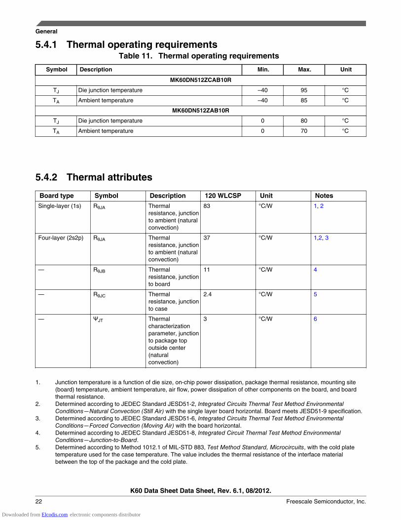
5.4.2 Thermal attributes
Board type Symbol Description 120 WLCSP Unit Notes
Single-layer (1s) RθJA Thermalresistance, junctionto ambient (naturalconvection)
83 °C/W 1, 2
Four-layer (2s2p) RθJA Thermalresistance, junctionto ambient (naturalconvection)
37 °C/W 1,2, 3
— RθJB Thermalresistance, junctionto board
11 °C/W 4
— RθJC Thermalresistance, junctionto case
2.4 °C/W 5
— ΨJT Thermalcharacterizationparameter, junctionto package topoutside center(naturalconvection)
3 °C/W 6
1. Junction temperature is a function of die size, on-chip power dissipation, package thermal resistance, mounting site(board) temperature, ambient temperature, air flow, power dissipation of other components on the board, and boardthermal resistance.
2. Determined according to JEDEC Standard JESD51-2, Integrated Circuits Thermal Test Method EnvironmentalConditions—Natural Convection (Still Air) with the single layer board horizontal. Board meets JESD51-9 specification.
3. Determined according to JEDEC Standard JESD51-6, Integrated Circuits Thermal Test Method EnvironmentalConditions—Forced Convection (Moving Air) with the board horizontal.
4. Determined according to JEDEC Standard JESD51-8, Integrated Circuit Thermal Test Method EnvironmentalConditions—Junction-to-Board.
5. Determined according to Method 1012.1 of MIL-STD 883, Test Method Standard, Microcircuits, with the cold platetemperature used for the case temperature. The value includes the thermal resistance of the interface materialbetween the top of the package and the cold plate.
General
K60 Data Sheet Data Sheet, Rev. 6.1, 08/2012.
22 Freescale Semiconductor, Inc.
Downloaded from Elcodis.com electronic components distributor
6. Determined according to JEDEC Standard JESD51-2, Integrated Circuits Thermal Test Method EnvironmentalConditions—Natural Convection (Still Air).
6 Peripheral operating requirements and behaviors
6.1 Core modules
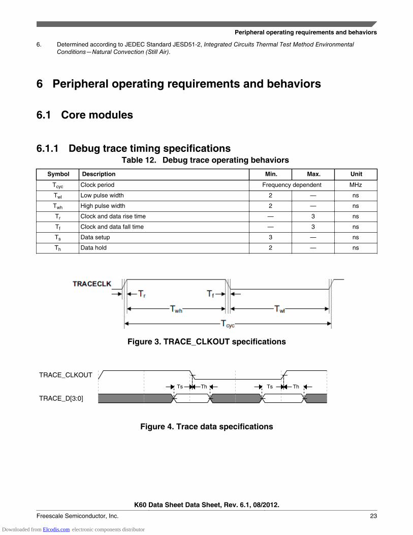
6.1.1 Debug trace timing specificationsTable 12. Debug trace operating behaviors
Symbol Description Min. Max. Unit
Tcyc Clock period Frequency dependent MHz
Twl Low pulse width 2 — ns
Twh High pulse width 2 — ns
Tr Clock and data rise time — 3 ns
Tf Clock and data fall time — 3 ns
Ts Data setup 3 — ns
Th Data hold 2 — ns
Figure 3. TRACE_CLKOUT specifications
ThTs Ts Th
TRACE_CLKOUT
TRACE_D[3:0]
Figure 4. Trace data specifications
Peripheral operating requirements and behaviors
K60 Data Sheet Data Sheet, Rev. 6.1, 08/2012.
Freescale Semiconductor, Inc. 23
Downloaded from Elcodis.com electronic components distributor
6.1.2 JTAG electricalsTable 13. JTAG limited voltage range electricals
Symbol Description Min. Max. Unit
Operating voltage 2.7 3.6 V
J1 TCLK frequency of operation
• Boundary Scan
• JTAG and CJTAG
• Serial Wire Debug
0
0
0
10
25
50
MHz
J2 TCLK cycle period 1/J1 — ns
J3 TCLK clock pulse width
• Boundary Scan
• JTAG and CJTAG
• Serial Wire Debug
50
20
10
—
—
—
ns
ns
ns
J4 TCLK rise and fall times — 3 ns
J5 Boundary scan input data setup time to TCLK rise 20 — ns
J6 Boundary scan input data hold time after TCLK rise 0 — ns
J7 TCLK low to boundary scan output data valid — 25 ns
J8 TCLK low to boundary scan output high-Z — 25 ns
J9 TMS, TDI input data setup time to TCLK rise 8 — ns
J10 TMS, TDI input data hold time after TCLK rise 1 — ns
J11 TCLK low to TDO data valid — 17 ns
J12 TCLK low to TDO high-Z — 17 ns
J13 TRST assert time 100 — ns
J14 TRST setup time (negation) to TCLK high 8 — ns
Table 14. JTAG full voltage range electricals
Symbol Description Min. Max. Unit
Operating voltage 1.71 3.6 V
J1 TCLK frequency of operation
• Boundary Scan
• JTAG and CJTAG
• Serial Wire Debug
0
0
0
10
20
40
MHz
J2 TCLK cycle period 1/J1 — ns
J3 TCLK clock pulse width
• Boundary Scan
• JTAG and CJTAG
• Serial Wire Debug
50
25
12.5
—
—
—
ns
ns
ns
J4 TCLK rise and fall times — 3 ns
Table continues on the next page...
Peripheral operating requirements and behaviors
K60 Data Sheet Data Sheet, Rev. 6.1, 08/2012.
24 Freescale Semiconductor, Inc.
Downloaded from Elcodis.com electronic components distributor
Table 14. JTAG full voltage range electricals (continued)
Symbol Description Min. Max. Unit
J5 Boundary scan input data setup time to TCLK rise 20 — ns
J6 Boundary scan input data hold time after TCLK rise 0 — ns
J7 TCLK low to boundary scan output data valid — 25 ns
J8 TCLK low to boundary scan output high-Z — 25 ns
J9 TMS, TDI input data setup time to TCLK rise 8 — ns
J10 TMS, TDI input data hold time after TCLK rise 1.4 — ns
J11 TCLK low to TDO data valid — 22.1 ns
J12 TCLK low to TDO high-Z — 22.1 ns
J13 TRST assert time 100 — ns
J14 TRST setup time (negation) to TCLK high 8 — ns
J2
J3 J3
J4 J4
TCLK (input)
Figure 5. Test clock input timing
J7
J8
J7
J5 J6
Input data valid
Output data valid
Output data valid
TCLK
Data inputs
Data outputs
Data outputs
Data outputs
Figure 6. Boundary scan (JTAG) timing
Peripheral operating requirements and behaviors
K60 Data Sheet Data Sheet, Rev. 6.1, 08/2012.
Freescale Semiconductor, Inc. 25
Downloaded from Elcodis.com electronic components distributor
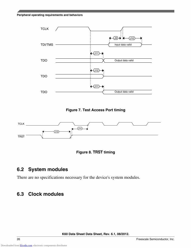
J11
J12
J11
J9 J10
Input data valid
Output data valid
Output data valid
TCLK
TDI/TMS
TDO
TDO
TDO
Figure 7. Test Access Port timing
J14
J13
TCLK
TRST
Figure 8. TRST timing
6.2 System modules
There are no specifications necessary for the device's system modules.
6.3 Clock modules
Peripheral operating requirements and behaviors
K60 Data Sheet Data Sheet, Rev. 6.1, 08/2012.
26 Freescale Semiconductor, Inc.
Downloaded from Elcodis.com electronic components distributor
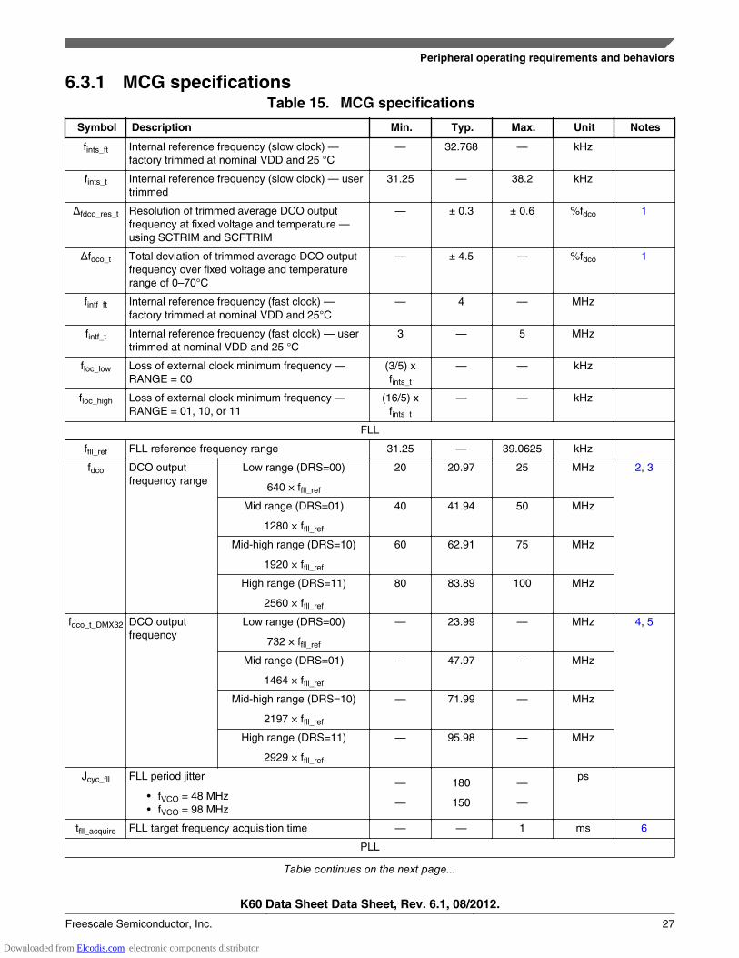
6.3.1 MCG specificationsTable 15. MCG specifications
Symbol Description Min. Typ. Max. Unit Notes
fints_ft Internal reference frequency (slow clock) —factory trimmed at nominal VDD and 25 °C
— 32.768 — kHz
fints_t Internal reference frequency (slow clock) — usertrimmed
31.25 — 38.2 kHz
Δfdco_res_t Resolution of trimmed average DCO outputfrequency at fixed voltage and temperature —using SCTRIM and SCFTRIM
— ± 0.3 ± 0.6 %fdco 1
Δfdco_t Total deviation of trimmed average DCO outputfrequency over fixed voltage and temperaturerange of 0–70°C
— ± 4.5 — %fdco 1
fintf_ft Internal reference frequency (fast clock) —factory trimmed at nominal VDD and 25°C
— 4 — MHz
fintf_t Internal reference frequency (fast clock) — usertrimmed at nominal VDD and 25 °C
3 — 5 MHz
floc_low Loss of external clock minimum frequency —RANGE = 00
(3/5) xfints_t
— — kHz
floc_high Loss of external clock minimum frequency —RANGE = 01, 10, or 11
(16/5) xfints_t
— — kHz
FLL
ffll_ref FLL reference frequency range 31.25 — 39.0625 kHz
fdco DCO outputfrequency range
Low range (DRS=00)
640 × ffll_ref
20 20.97 25 MHz 2, 3
Mid range (DRS=01)
1280 × ffll_ref
40 41.94 50 MHz
Mid-high range (DRS=10)
1920 × ffll_ref
60 62.91 75 MHz
High range (DRS=11)
2560 × ffll_ref
80 83.89 100 MHz
fdco_t_DMX32 DCO outputfrequency
Low range (DRS=00)
732 × ffll_ref
— 23.99 — MHz 4, 5
Mid range (DRS=01)
1464 × ffll_ref
— 47.97 — MHz
Mid-high range (DRS=10)
2197 × ffll_ref
— 71.99 — MHz
High range (DRS=11)
2929 × ffll_ref
— 95.98 — MHz
Jcyc_fll FLL period jitter
• fVCO = 48 MHz• fVCO = 98 MHz
—
—
180
150
—
—
ps
tfll_acquire FLL target frequency acquisition time — — 1 ms 6
PLL
Table continues on the next page...
Peripheral operating requirements and behaviors
K60 Data Sheet Data Sheet, Rev. 6.1, 08/2012.
Freescale Semiconductor, Inc. 27
Downloaded from Elcodis.com electronic components distributor
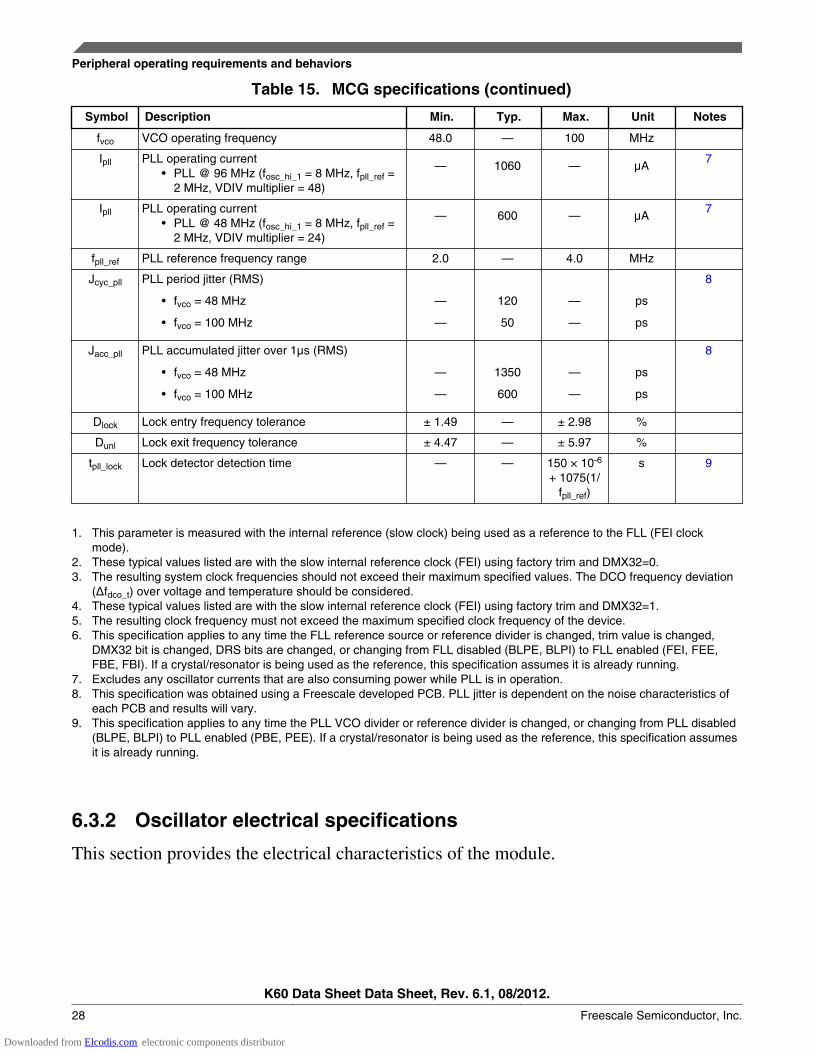
Table 15. MCG specifications (continued)
Symbol Description Min. Typ. Max. Unit Notes
fvco VCO operating frequency 48.0 — 100 MHz
Ipll PLL operating current• PLL @ 96 MHz (fosc_hi_1 = 8 MHz, fpll_ref =
2 MHz, VDIV multiplier = 48)
— 1060 — µA7
Ipll PLL operating current• PLL @ 48 MHz (fosc_hi_1 = 8 MHz, fpll_ref =
2 MHz, VDIV multiplier = 24)
— 600 — µA7
fpll_ref PLL reference frequency range 2.0 — 4.0 MHz
Jcyc_pll PLL period jitter (RMS)
• fvco = 48 MHz
• fvco = 100 MHz
—
—
120
50
—
—
ps
ps
8
Jacc_pll PLL accumulated jitter over 1µs (RMS)
• fvco = 48 MHz
• fvco = 100 MHz
—
—
1350
600
—
—
ps
ps
8
Dlock Lock entry frequency tolerance ± 1.49 — ± 2.98 %
Dunl Lock exit frequency tolerance ± 4.47 — ± 5.97 %
tpll_lock Lock detector detection time — — 150 × 10-6
+ 1075(1/fpll_ref)
s 9
1. This parameter is measured with the internal reference (slow clock) being used as a reference to the FLL (FEI clockmode).
2. These typical values listed are with the slow internal reference clock (FEI) using factory trim and DMX32=0.3. The resulting system clock frequencies should not exceed their maximum specified values. The DCO frequency deviation
(Δfdco_t) over voltage and temperature should be considered.4. These typical values listed are with the slow internal reference clock (FEI) using factory trim and DMX32=1.5. The resulting clock frequency must not exceed the maximum specified clock frequency of the device.6. This specification applies to any time the FLL reference source or reference divider is changed, trim value is changed,
DMX32 bit is changed, DRS bits are changed, or changing from FLL disabled (BLPE, BLPI) to FLL enabled (FEI, FEE,FBE, FBI). If a crystal/resonator is being used as the reference, this specification assumes it is already running.
7. Excludes any oscillator currents that are also consuming power while PLL is in operation.8. This specification was obtained using a Freescale developed PCB. PLL jitter is dependent on the noise characteristics of
each PCB and results will vary.9. This specification applies to any time the PLL VCO divider or reference divider is changed, or changing from PLL disabled
(BLPE, BLPI) to PLL enabled (PBE, PEE). If a crystal/resonator is being used as the reference, this specification assumesit is already running.
6.3.2 Oscillator electrical specifications
This section provides the electrical characteristics of the module.
Peripheral operating requirements and behaviors
K60 Data Sheet Data Sheet, Rev. 6.1, 08/2012.
28 Freescale Semiconductor, Inc.
Downloaded from Elcodis.com electronic components distributor
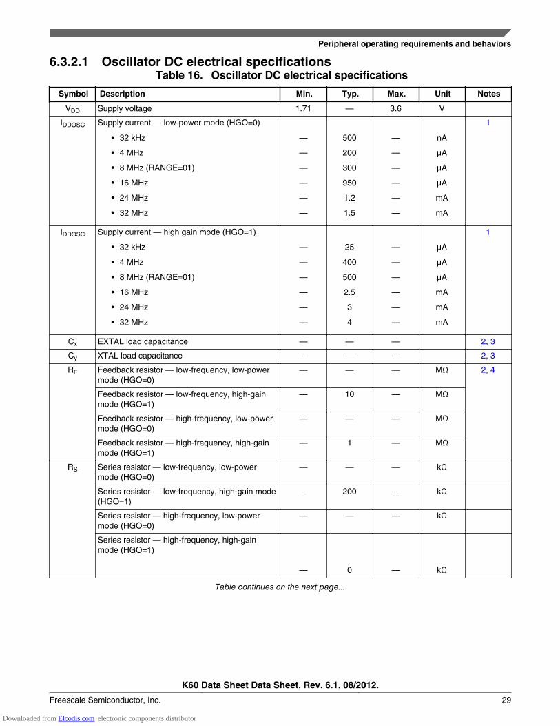
6.3.2.1 Oscillator DC electrical specificationsTable 16. Oscillator DC electrical specifications
Symbol Description Min. Typ. Max. Unit Notes
VDD Supply voltage 1.71 — 3.6 V
IDDOSC Supply current — low-power mode (HGO=0)
• 32 kHz
• 4 MHz
• 8 MHz (RANGE=01)
• 16 MHz
• 24 MHz
• 32 MHz
—
—
—
—
—
—
500
200
300
950
1.2
1.5
—
—
—
—
—
—
nA
μA
μA
μA
mA
mA
1
IDDOSC Supply current — high gain mode (HGO=1)
• 32 kHz
• 4 MHz
• 8 MHz (RANGE=01)
• 16 MHz
• 24 MHz
• 32 MHz
—
—
—
—
—
—
25
400
500
2.5
3
4
—
—
—
—
—
—
μA
μA
μA
mA
mA
mA
1
Cx EXTAL load capacitance — — — 2, 3
Cy XTAL load capacitance — — — 2, 3
RF Feedback resistor — low-frequency, low-powermode (HGO=0)
— — — MΩ 2, 4
Feedback resistor — low-frequency, high-gainmode (HGO=1)
— 10 — MΩ
Feedback resistor — high-frequency, low-powermode (HGO=0)
— — — MΩ
Feedback resistor — high-frequency, high-gainmode (HGO=1)
— 1 — MΩ
RS Series resistor — low-frequency, low-powermode (HGO=0)
— — — kΩ
Series resistor — low-frequency, high-gain mode(HGO=1)
— 200 — kΩ
Series resistor — high-frequency, low-powermode (HGO=0)
— — — kΩ
Series resistor — high-frequency, high-gainmode (HGO=1)
—
0
—
kΩ
Table continues on the next page...
Peripheral operating requirements and behaviors
K60 Data Sheet Data Sheet, Rev. 6.1, 08/2012.
Freescale Semiconductor, Inc. 29
Downloaded from Elcodis.com electronic components distributor
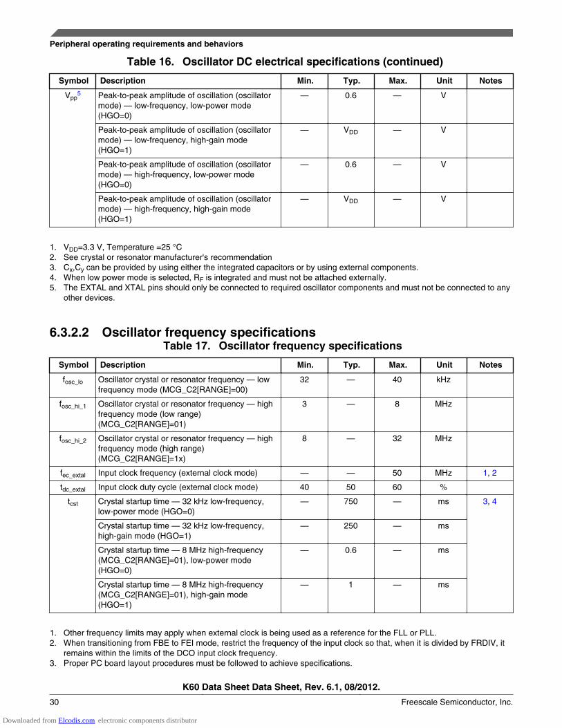
Table 16. Oscillator DC electrical specifications (continued)
Symbol Description Min. Typ. Max. Unit Notes
Vpp5 Peak-to-peak amplitude of oscillation (oscillator
mode) — low-frequency, low-power mode(HGO=0)
— 0.6 — V
Peak-to-peak amplitude of oscillation (oscillatormode) — low-frequency, high-gain mode(HGO=1)
— VDD — V
Peak-to-peak amplitude of oscillation (oscillatormode) — high-frequency, low-power mode(HGO=0)
— 0.6 — V
Peak-to-peak amplitude of oscillation (oscillatormode) — high-frequency, high-gain mode(HGO=1)
— VDD — V
1. VDD=3.3 V, Temperature =25 °C2. See crystal or resonator manufacturer's recommendation3. Cx,Cy can be provided by using either the integrated capacitors or by using external components.4. When low power mode is selected, RF is integrated and must not be attached externally.5. The EXTAL and XTAL pins should only be connected to required oscillator components and must not be connected to any
other devices.
6.3.2.2 Oscillator frequency specificationsTable 17. Oscillator frequency specifications
Symbol Description Min. Typ. Max. Unit Notes
fosc_lo Oscillator crystal or resonator frequency — lowfrequency mode (MCG_C2[RANGE]=00)
32 — 40 kHz
fosc_hi_1 Oscillator crystal or resonator frequency — highfrequency mode (low range)(MCG_C2[RANGE]=01)
3 — 8 MHz
fosc_hi_2 Oscillator crystal or resonator frequency — highfrequency mode (high range)(MCG_C2[RANGE]=1x)
8 — 32 MHz
fec_extal Input clock frequency (external clock mode) — — 50 MHz 1, 2
tdc_extal Input clock duty cycle (external clock mode) 40 50 60 %
tcst Crystal startup time — 32 kHz low-frequency,low-power mode (HGO=0)
— 750 — ms 3, 4
Crystal startup time — 32 kHz low-frequency,high-gain mode (HGO=1)
— 250 — ms
Crystal startup time — 8 MHz high-frequency(MCG_C2[RANGE]=01), low-power mode(HGO=0)
— 0.6 — ms
Crystal startup time — 8 MHz high-frequency(MCG_C2[RANGE]=01), high-gain mode(HGO=1)
— 1 — ms
1. Other frequency limits may apply when external clock is being used as a reference for the FLL or PLL.2. When transitioning from FBE to FEI mode, restrict the frequency of the input clock so that, when it is divided by FRDIV, it
remains within the limits of the DCO input clock frequency.3. Proper PC board layout procedures must be followed to achieve specifications.
Peripheral operating requirements and behaviors
K60 Data Sheet Data Sheet, Rev. 6.1, 08/2012.
30 Freescale Semiconductor, Inc.
Downloaded from Elcodis.com electronic components distributor
4. Crystal startup time is defined as the time between the oscillator being enabled and the OSCINIT bit in the MCG_S registerbeing set.
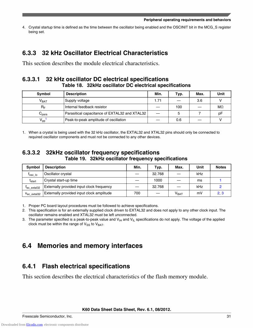
6.3.3 32 kHz Oscillator Electrical Characteristics
This section describes the module electrical characteristics.
6.3.3.1 32 kHz oscillator DC electrical specificationsTable 18. 32kHz oscillator DC electrical specifications
Symbol Description Min. Typ. Max. Unit
VBAT Supply voltage 1.71 — 3.6 V
RF Internal feedback resistor — 100 — MΩ
Cpara Parasitical capacitance of EXTAL32 and XTAL32 — 5 7 pF
Vpp1 Peak-to-peak amplitude of oscillation — 0.6 — V
1. When a crystal is being used with the 32 kHz oscillator, the EXTAL32 and XTAL32 pins should only be connected torequired oscillator components and must not be connected to any other devices.
6.3.3.2 32kHz oscillator frequency specificationsTable 19. 32kHz oscillator frequency specifications
Symbol Description Min. Typ. Max. Unit Notes
fosc_lo Oscillator crystal — 32.768 — kHz
tstart Crystal start-up time — 1000 — ms 1
fec_extal32 Externally provided input clock frequency — 32.768 — kHz 2
vec_extal32 Externally provided input clock amplitude 700 — VBAT mV 2, 3
1. Proper PC board layout procedures must be followed to achieve specifications.2. This specification is for an externally supplied clock driven to EXTAL32 and does not apply to any other clock input. The
oscillator remains enabled and XTAL32 must be left unconnected.3. The parameter specified is a peak-to-peak value and VIH and VIL specifications do not apply. The voltage of the applied
clock must be within the range of VSS to VBAT.
6.4 Memories and memory interfaces
6.4.1 Flash electrical specifications
This section describes the electrical characteristics of the flash memory module.
Peripheral operating requirements and behaviors
K60 Data Sheet Data Sheet, Rev. 6.1, 08/2012.
Freescale Semiconductor, Inc. 31
Downloaded from Elcodis.com electronic components distributor
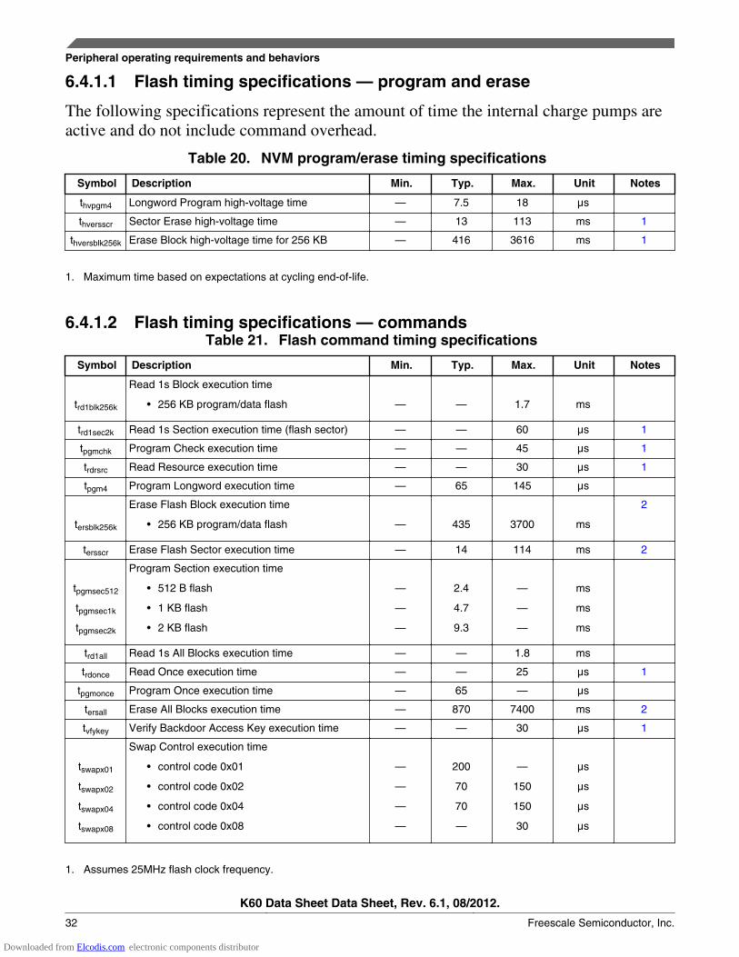
6.4.1.1 Flash timing specifications — program and erase
The following specifications represent the amount of time the internal charge pumps areactive and do not include command overhead.
Table 20. NVM program/erase timing specifications
Symbol Description Min. Typ. Max. Unit Notes
thvpgm4 Longword Program high-voltage time — 7.5 18 μs
thversscr Sector Erase high-voltage time — 13 113 ms 1
thversblk256k Erase Block high-voltage time for 256 KB — 416 3616 ms 1
1. Maximum time based on expectations at cycling end-of-life.
6.4.1.2 Flash timing specifications — commandsTable 21. Flash command timing specifications
Symbol Description Min. Typ. Max. Unit Notes
trd1blk256k
Read 1s Block execution time
• 256 KB program/data flash
—
—
1.7
ms
trd1sec2k Read 1s Section execution time (flash sector) — — 60 μs 1
tpgmchk Program Check execution time — — 45 μs 1
trdrsrc Read Resource execution time — — 30 μs 1
tpgm4 Program Longword execution time — 65 145 μs
tersblk256k
Erase Flash Block execution time
• 256 KB program/data flash
—
435
3700
ms
2
tersscr Erase Flash Sector execution time — 14 114 ms 2
tpgmsec512
tpgmsec1k
tpgmsec2k
Program Section execution time
• 512 B flash
• 1 KB flash
• 2 KB flash
—
—
—
2.4
4.7
9.3
—
—
—
ms
ms
ms
trd1all Read 1s All Blocks execution time — — 1.8 ms
trdonce Read Once execution time — — 25 μs 1
tpgmonce Program Once execution time — 65 — μs
tersall Erase All Blocks execution time — 870 7400 ms 2
tvfykey Verify Backdoor Access Key execution time — — 30 μs 1
tswapx01
tswapx02
tswapx04
tswapx08
Swap Control execution time
• control code 0x01
• control code 0x02
• control code 0x04
• control code 0x08
—
—
—
—
200
70
70
—
—
150
150
30
μs
μs
μs
μs
1. Assumes 25MHz flash clock frequency.
Peripheral operating requirements and behaviors
K60 Data Sheet Data Sheet, Rev. 6.1, 08/2012.
32 Freescale Semiconductor, Inc.
Downloaded from Elcodis.com electronic components distributor
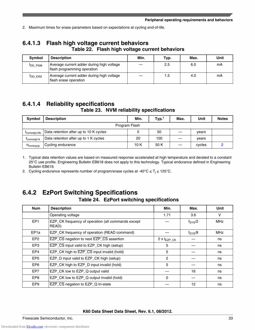
2. Maximum times for erase parameters based on expectations at cycling end-of-life.
6.4.1.3 Flash high voltage current behaviorsTable 22. Flash high voltage current behaviors
Symbol Description Min. Typ. Max. Unit
IDD_PGM Average current adder during high voltageflash programming operation
— 2.5 6.0 mA
IDD_ERS Average current adder during high voltageflash erase operation
— 1.5 4.0 mA
6.4.1.4 Reliability specificationsTable 23. NVM reliability specifications
Symbol Description Min. Typ.1 Max. Unit Notes
Program Flash
tnvmretp10k Data retention after up to 10 K cycles 5 50 — years
tnvmretp1k Data retention after up to 1 K cycles 20 100 — years
nnvmcycp Cycling endurance 10 K 50 K — cycles 2
1. Typical data retention values are based on measured response accelerated at high temperature and derated to a constant25°C use profile. Engineering Bulletin EB618 does not apply to this technology. Typical endurance defined in EngineeringBulletin EB619.
2. Cycling endurance represents number of program/erase cycles at -40°C ≤ Tj ≤ 125°C.
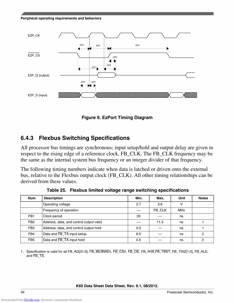
6.4.2 EzPort Switching SpecificationsTable 24. EzPort switching specifications
Num Description Min. Max. Unit
Operating voltage 1.71 3.6 V
EP1 EZP_CK frequency of operation (all commands exceptREAD)
— fSYS/2 MHz
EP1a EZP_CK frequency of operation (READ command) — fSYS/8 MHz
EP2 EZP_CS negation to next EZP_CS assertion 2 x tEZP_CK — ns
EP3 EZP_CS input valid to EZP_CK high (setup) 5 — ns
EP4 EZP_CK high to EZP_CS input invalid (hold) 5 — ns
EP5 EZP_D input valid to EZP_CK high (setup) 2 — ns
EP6 EZP_CK high to EZP_D input invalid (hold) 5 — ns
EP7 EZP_CK low to EZP_Q output valid — 16 ns
EP8 EZP_CK low to EZP_Q output invalid (hold) 0 — ns
EP9 EZP_CS negation to EZP_Q tri-state — 12 ns
Peripheral operating requirements and behaviors
K60 Data Sheet Data Sheet, Rev. 6.1, 08/2012.
Freescale Semiconductor, Inc. 33
Downloaded from Elcodis.com electronic components distributor
EP2EP3 EP4
EP5 EP6
EP7EP8
EP9
EZP_CK
EZP_CS
EZP_Q (output)
EZP_D (input)
Figure 9. EzPort Timing Diagram
6.4.3 Flexbus Switching Specifications
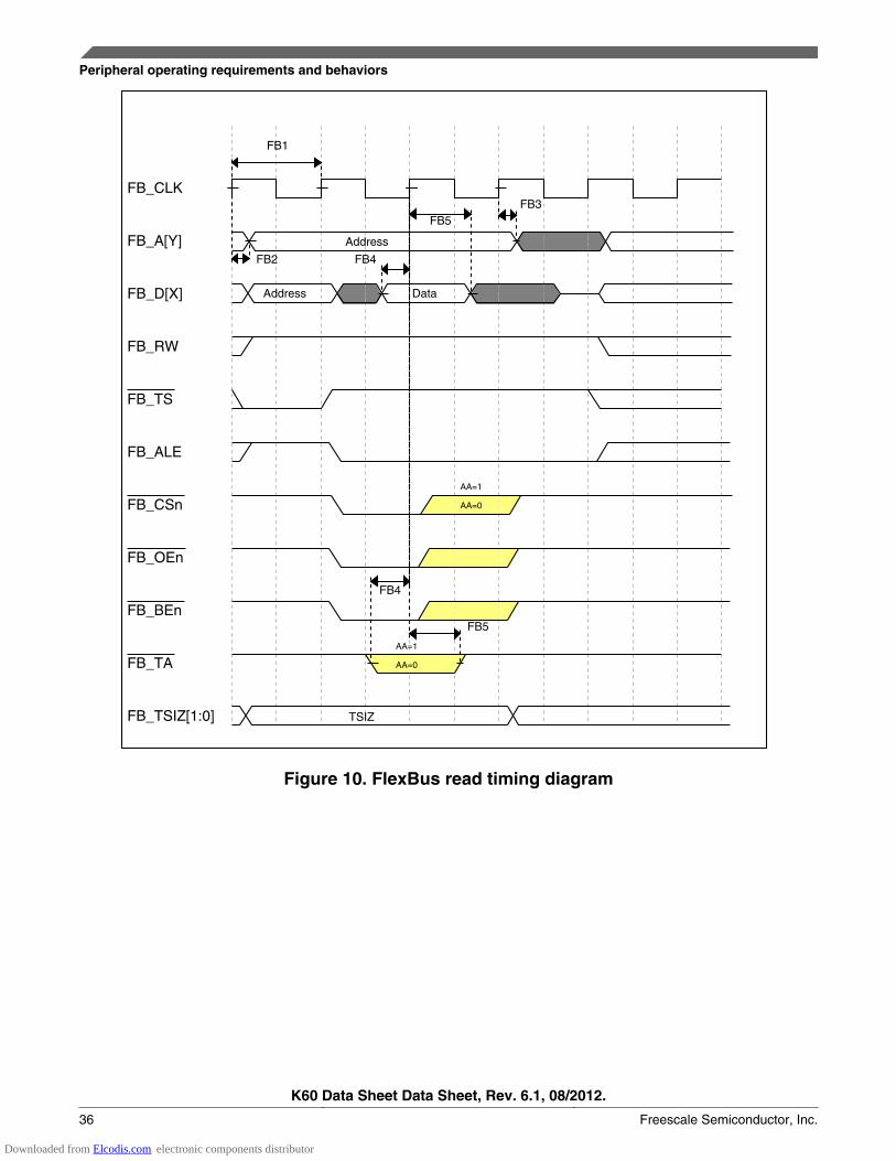
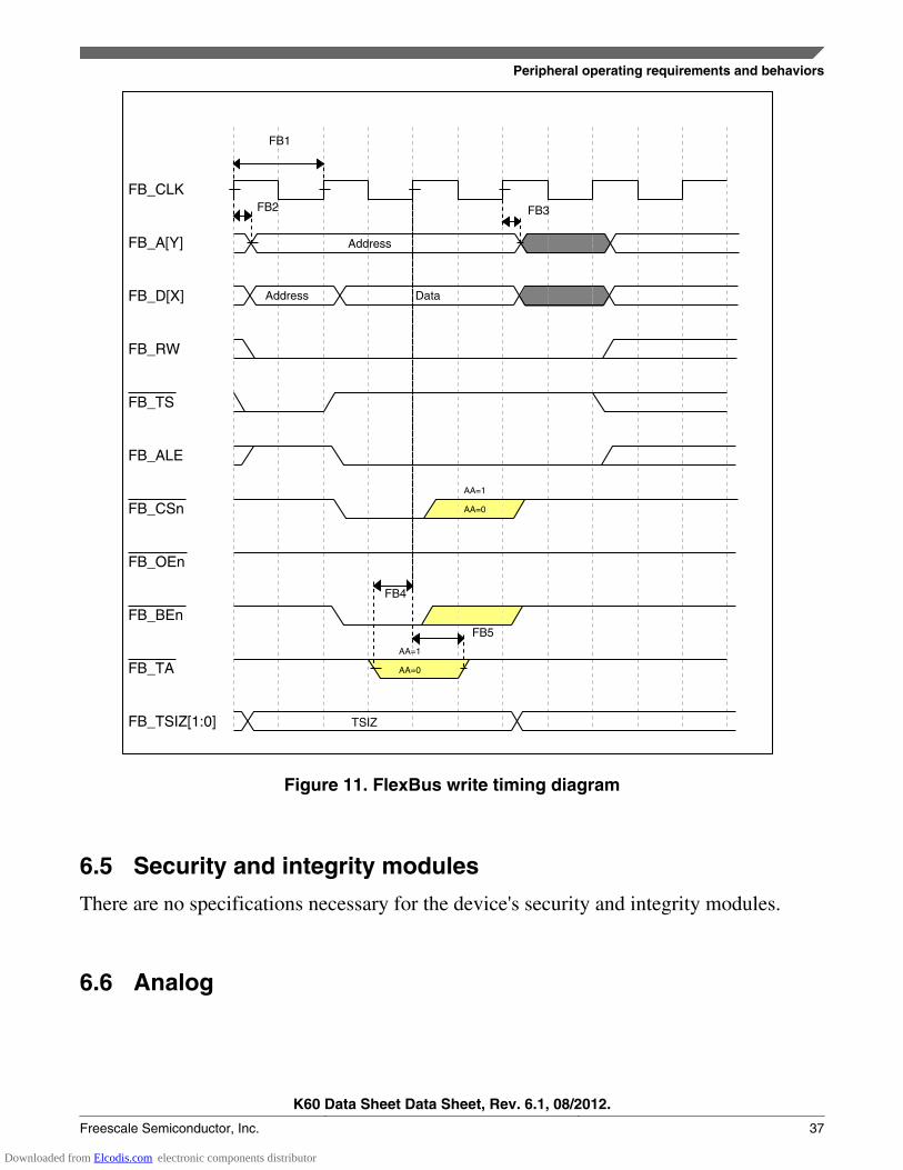
All processor bus timings are synchronous; input setup/hold and output delay are given inrespect to the rising edge of a reference clock, FB_CLK. The FB_CLK frequency may bethe same as the internal system bus frequency or an integer divider of that frequency.
The following timing numbers indicate when data is latched or driven onto the externalbus, relative to the Flexbus output clock (FB_CLK). All other timing relationships can bederived from these values.
Table 25. Flexbus limited voltage range switching specifications
Num Description Min. Max. Unit Notes
Operating voltage 2.7 3.6 V
Frequency of operation — FB_CLK MHz
FB1 Clock period 20 — ns
FB2 Address, data, and control output valid — 11.5 ns 1
FB3 Address, data, and control output hold 0.5 — ns 1
FB4 Data and FB_TA input setup 8.5 — ns 2
FB5 Data and FB_TA input hold 0.5 — ns 2
1. Specification is valid for all FB_AD[31:0], FB_BE/BWEn, FB_CSn, FB_OE, FB_R/W,FB_TBST, FB_TSIZ[1:0], FB_ALE,and FB_TS.
Peripheral operating requirements and behaviors
K60 Data Sheet Data Sheet, Rev. 6.1, 08/2012.
34 Freescale Semiconductor, Inc.
Downloaded from Elcodis.com electronic components distributor
2. Specification is valid for all FB_AD[31:0] and FB_TA.
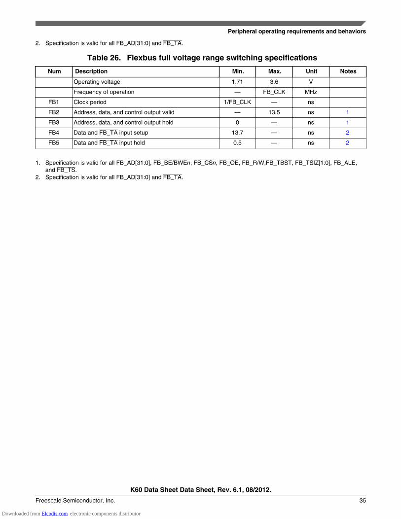
Table 26. Flexbus full voltage range switching specifications
Num Description Min. Max. Unit Notes
Operating voltage 1.71 3.6 V
Frequency of operation — FB_CLK MHz
FB1 Clock period 1/FB_CLK — ns
FB2 Address, data, and control output valid — 13.5 ns 1
FB3 Address, data, and control output hold 0 — ns 1
FB4 Data and FB_TA input setup 13.7 — ns 2
FB5 Data and FB_TA input hold 0.5 — ns 2
1. Specification is valid for all FB_AD[31:0], FB_BE/BWEn, FB_CSn, FB_OE, FB_R/W,FB_TBST, FB_TSIZ[1:0], FB_ALE,and FB_TS.
2. Specification is valid for all FB_AD[31:0] and FB_TA.
Peripheral operating requirements and behaviors
K60 Data Sheet Data Sheet, Rev. 6.1, 08/2012.
Freescale Semiconductor, Inc. 35
Downloaded from Elcodis.com electronic components distributor
Address
Address Data
TSIZ
AA=1
AA=0
AA=1
AA=0
FB1
FB3FB5
FB4
FB4
FB5
FB2
FB_CLK
FB_A[Y]
FB_D[X]
FB_RW
FB_TS
FB_ALE
FB_CSn
FB_OEn
FB_BEn
FB_TA
FB_TSIZ[1:0]
Figure 10. FlexBus read timing diagram
Peripheral operating requirements and behaviors
K60 Data Sheet Data Sheet, Rev. 6.1, 08/2012.
36 Freescale Semiconductor, Inc.
Downloaded from Elcodis.com electronic components distributor
Address
Address Data
TSIZ
AA=1
AA=0
AA=1
AA=0
FB1
FB3
FB4
FB5
FB2FB_CLK
FB_A[Y]
FB_D[X]
FB_RW
FB_TS
FB_ALE
FB_CSn
FB_OEn
FB_BEn
FB_TA
FB_TSIZ[1:0]
Figure 11. FlexBus write timing diagram
6.5 Security and integrity modules
There are no specifications necessary for the device's security and integrity modules.
6.6 Analog
Peripheral operating requirements and behaviors
K60 Data Sheet Data Sheet, Rev. 6.1, 08/2012.
Freescale Semiconductor, Inc. 37
Downloaded from Elcodis.com electronic components distributor
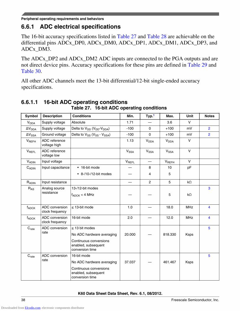
6.6.1 ADC electrical specifications
The 16-bit accuracy specifications listed in Table 27 and Table 28 are achievable on thedifferential pins ADCx_DP0, ADCx_DM0, ADCx_DP1, ADCx_DM1, ADCx_DP3, andADCx_DM3.
The ADCx_DP2 and ADCx_DM2 ADC inputs are connected to the PGA outputs and arenot direct device pins. Accuracy specifications for these pins are defined in Table 29 andTable 30.
All other ADC channels meet the 13-bit differential/12-bit single-ended accuracyspecifications.
6.6.1.1 16-bit ADC operating conditionsTable 27. 16-bit ADC operating conditions
Symbol Description Conditions Min. Typ.1 Max. Unit Notes
VDDA Supply voltage Absolute 1.71 — 3.6 V
ΔVDDA Supply voltage Delta to VDD (VDD-VDDA) -100 0 +100 mV 2
ΔVSSA Ground voltage Delta to VSS (VSS - VSSA) -100 0 +100 mV 2
VREFH ADC referencevoltage high
1.13 VDDA VDDA V
VREFL ADC referencevoltage low
VSSA VSSA VSSA V
VADIN Input voltage VREFL — VREFH V
CADIN Input capacitance • 16-bit mode
• 8-/10-/12-bit modes
—
—
8
4
10
5
pF
RADIN Input resistance — 2 5 kΩ
RAS Analog sourceresistance
13-/12-bit modes
fADCK < 4 MHz
—
—
5
kΩ
3
fADCK ADC conversionclock frequency
≤ 13-bit mode 1.0 — 18.0 MHz 4
fADCK ADC conversionclock frequency
16-bit mode 2.0 — 12.0 MHz 4
Crate ADC conversionrate
≤ 13 bit modes
No ADC hardware averaging
Continuous conversionsenabled, subsequentconversion time
20.000
—
818.330
Ksps
5
Crate ADC conversionrate
16-bit mode
No ADC hardware averaging
Continuous conversionsenabled, subsequentconversion time
37.037
—
461.467
Ksps
5
Peripheral operating requirements and behaviors
K60 Data Sheet Data Sheet, Rev. 6.1, 08/2012.
38 Freescale Semiconductor, Inc.
Downloaded from Elcodis.com electronic components distributor
1. Typical values assume VDDA = 3.0 V, Temp = 25 °C, fADCK = 1.0 MHz unless otherwise stated. Typical values are forreference only and are not tested in production.
2. DC potential difference.3. This resistance is external to MCU. The analog source resistance must be kept as low as possible to achieve the best
results. The results in this data sheet were derived from a system which has < 8 Ω analog source resistance. The RAS/CAStime constant should be kept to < 1ns.
4. To use the maximum ADC conversion clock frequency, the ADHSC bit must be set and the ADLPC bit must be clear.5. For guidelines and examples of conversion rate calculation, download the ADC calculator tool: http://cache.freescale.com/
files/soft_dev_tools/software/app_software/converters/ADC_CALCULATOR_CNV.zip?fpsp=1
RAS
VASCAS
ZAS
VADIN
ZADIN
RADIN
RADIN
RADIN
RADIN
CADIN
Pad leakagedue toinput protection
INPUT PININPUT PIN
INPUT PIN
INPUT PIN
SIMPLIFIEDINPUT PIN EQUIVALENT
CIRCUITSIMPLIFIED
CHANNEL SELECTCIRCUIT ADC SAR
ENGINE
Figure 12. ADC input impedance equivalency diagram
6.6.1.2 16-bit ADC electrical characteristicsTable 28. 16-bit ADC characteristics (VREFH = VDDA, VREFL = VSSA)
Symbol Description Conditions1 Min. Typ.2 Max. Unit Notes
IDDA_ADC Supply current 0.215 — 1.7 mA 3
fADACK
ADCasynchronousclock source
• ADLPC = 1, ADHSC = 0
• ADLPC = 1, ADHSC = 1
• ADLPC = 0, ADHSC = 0
• ADLPC = 0, ADHSC = 1
1.2
2.4
3.0
4.4
2.4
4.0
5.2
6.2
3.9
6.1
7.3
9.5
MHz
MHz
MHz
MHz
tADACK = 1/fADACK
Sample Time See Reference Manual chapter for sample times
TUE Total unadjustederror
• 12-bit modes
• <12-bit modes
—
—
±4
±1.4
±6.8
±2.1
LSB4 5
Table continues on the next page...
Peripheral operating requirements and behaviors
K60 Data Sheet Data Sheet, Rev. 6.1, 08/2012.
Freescale Semiconductor, Inc. 39
Downloaded from Elcodis.com electronic components distributor
Table 28. 16-bit ADC characteristics (VREFH = VDDA, VREFL = VSSA) (continued)
Symbol Description Conditions1 Min. Typ.2 Max. Unit Notes
DNL Differential non-linearity
• 12-bit modes
• <12-bit modes
—
—
±0.7
±0.2
-1.1 to +1.9
-0.3 to 0.5
LSB4 5
INL Integral non-linearity
• 12-bit modes
• <12-bit modes
—
—
±1.0
±0.5
-2.7 to +1.9
-0.7 to +0.5
LSB4 5
EFS Full-scale error • 12-bit modes
• <12-bit modes
—
—
-4
-1.4
-5.4
-1.8
LSB4 VADIN =VDDA
5
EQ Quantizationerror
• 16-bit modes
• ≤13-bit modes
—
—
-1 to 0
—
—
±0.5
LSB4
ENOB Effective numberof bits
16-bit differential mode
• Avg = 32
• Avg = 4
16-bit single-ended mode
• Avg = 32
• Avg = 4
12.8
11.9
12.2
11.4
14.5
13.8
13.9
13.1
—
—
—
—
bits
bits
bits
bits
6
SINADSignal-to-noiseplus distortion
See ENOB6.02 × ENOB + 1.76 dB
THD Total harmonicdistortion
16-bit differential mode
• Avg = 32
16-bit single-ended mode
• Avg = 32
—
—
–94
-85
—
—
dB
dB
7
SFDR Spurious freedynamic range
16-bit differential mode
• Avg = 32
16-bit single-ended mode
• Avg = 32
82
78
95
90
—
—
dB
dB
7
EIL Input leakageerror
IIn × RAS mV IIn =leakagecurrent
(refer tothe MCU's
voltageand currentoperatingratings)
Temp sensorslope
Across the full temperaturerange of the device
— 1.715 — mV/°C
Table continues on the next page...
Peripheral operating requirements and behaviors
K60 Data Sheet Data Sheet, Rev. 6.1, 08/2012.
40 Freescale Semiconductor, Inc.
Downloaded from Elcodis.com electronic components distributor
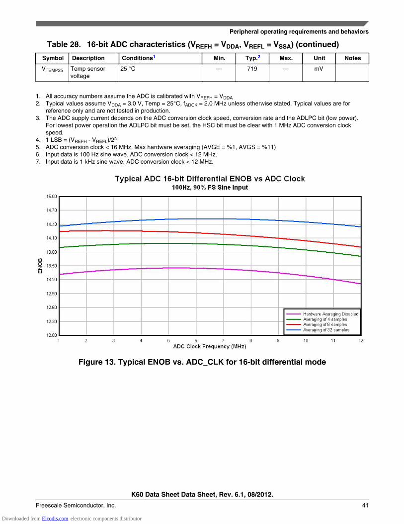
Table 28. 16-bit ADC characteristics (VREFH = VDDA, VREFL = VSSA) (continued)
Symbol Description Conditions1 Min. Typ.2 Max. Unit Notes
VTEMP25 Temp sensorvoltage
25 °C — 719 — mV
1. All accuracy numbers assume the ADC is calibrated with VREFH = VDDA2. Typical values assume VDDA = 3.0 V, Temp = 25°C, fADCK = 2.0 MHz unless otherwise stated. Typical values are for
reference only and are not tested in production.3. The ADC supply current depends on the ADC conversion clock speed, conversion rate and the ADLPC bit (low power).
For lowest power operation the ADLPC bit must be set, the HSC bit must be clear with 1 MHz ADC conversion clockspeed.
4. 1 LSB = (VREFH - VREFL)/2N
5. ADC conversion clock < 16 MHz, Max hardware averaging (AVGE = %1, AVGS = %11)6. Input data is 100 Hz sine wave. ADC conversion clock < 12 MHz.7. Input data is 1 kHz sine wave. ADC conversion clock < 12 MHz.
Figure 13. Typical ENOB vs. ADC_CLK for 16-bit differential mode
Peripheral operating requirements and behaviors
K60 Data Sheet Data Sheet, Rev. 6.1, 08/2012.
Freescale Semiconductor, Inc. 41
Downloaded from Elcodis.com electronic components distributor
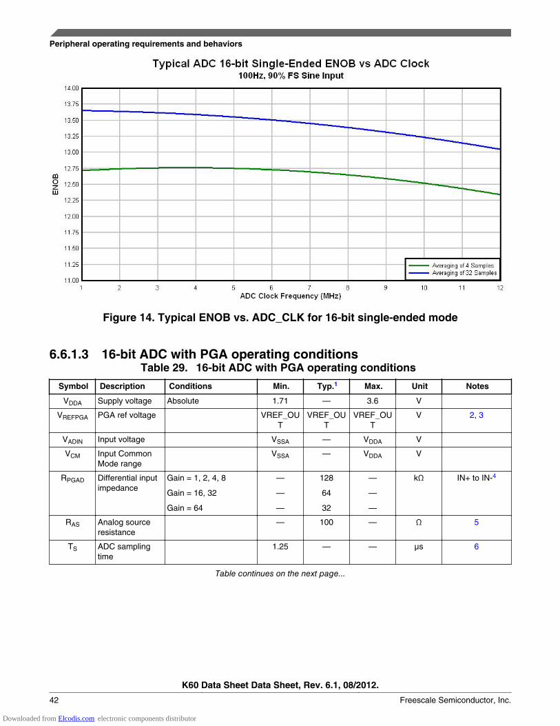
Figure 14. Typical ENOB vs. ADC_CLK for 16-bit single-ended mode
6.6.1.3 16-bit ADC with PGA operating conditionsTable 29. 16-bit ADC with PGA operating conditions
Symbol Description Conditions Min. Typ.1 Max. Unit Notes
VDDA Supply voltage Absolute 1.71 — 3.6 V
VREFPGA PGA ref voltage VREF_OUT
VREF_OUT
VREF_OUT
V 2, 3
VADIN Input voltage VSSA — VDDA V
VCM Input CommonMode range
VSSA — VDDA V
RPGAD Differential inputimpedance
Gain = 1, 2, 4, 8
Gain = 16, 32
Gain = 64
—
—
—
128
64
32
—
—
—
kΩ IN+ to IN-4
RAS Analog sourceresistance
— 100 — Ω 5
TS ADC samplingtime
1.25 — — µs 6
Table continues on the next page...
Peripheral operating requirements and behaviors
K60 Data Sheet Data Sheet, Rev. 6.1, 08/2012.
42 Freescale Semiconductor, Inc.
Downloaded from Elcodis.com electronic components distributor
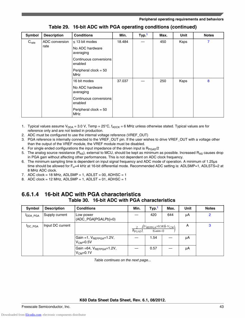
Table 29. 16-bit ADC with PGA operating conditions (continued)
Symbol Description Conditions Min. Typ.1 Max. Unit Notes
Crate ADC conversionrate
≤ 13 bit modes
No ADC hardwareaveraging
Continuous conversionsenabled
Peripheral clock = 50MHz
18.484 — 450 Ksps 7
16 bit modes
No ADC hardwareaveraging
Continuous conversionsenabled
Peripheral clock = 50MHz
37.037 — 250 Ksps 8
1. Typical values assume VDDA = 3.0 V, Temp = 25°C, fADCK = 6 MHz unless otherwise stated. Typical values are forreference only and are not tested in production.
2. ADC must be configured to use the internal voltage reference (VREF_OUT)3. PGA reference is internally connected to the VREF_OUT pin. If the user wishes to drive VREF_OUT with a voltage other
than the output of the VREF module, the VREF module must be disabled.4. For single ended configurations the input impedance of the driven input is RPGAD/25. The analog source resistance (RAS), external to MCU, should be kept as minimum as possible. Increased RAS causes drop
in PGA gain without affecting other performances. This is not dependent on ADC clock frequency.6. The minimum sampling time is dependent on input signal frequency and ADC mode of operation. A minimum of 1.25µs
time should be allowed for Fin=4 kHz at 16-bit differential mode. Recommended ADC setting is: ADLSMP=1, ADLSTS=2 at8 MHz ADC clock.
7. ADC clock = 18 MHz, ADLSMP = 1, ADLST = 00, ADHSC = 18. ADC clock = 12 MHz, ADLSMP = 1, ADLST = 01, ADHSC = 1
6.6.1.4 16-bit ADC with PGA characteristicsTable 30. 16-bit ADC with PGA characteristics
Symbol Description Conditions Min. Typ.1 Max. Unit Notes
IDDA_PGA Supply current Low power(ADC_PGA[PGALPb]=0)
— 420 644 μA 2
IDC_PGA Input DC current A 3
Gain =1, VREFPGA=1.2V,VCM=0.5V
— 1.54 — μA
Gain =64, VREFPGA=1.2V,VCM=0.1V
— 0.57 — μA
Table continues on the next page...
Peripheral operating requirements and behaviors
K60 Data Sheet Data Sheet, Rev. 6.1, 08/2012.
Freescale Semiconductor, Inc. 43
Downloaded from Elcodis.com electronic components distributor
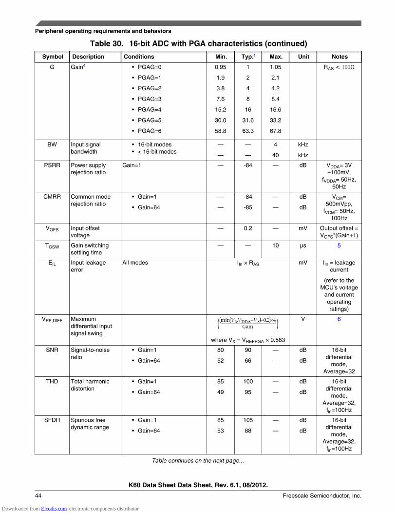
Table 30. 16-bit ADC with PGA characteristics (continued)
Symbol Description Conditions Min. Typ.1 Max. Unit Notes
G Gain4 • PGAG=0
• PGAG=1
• PGAG=2
• PGAG=3
• PGAG=4
• PGAG=5
• PGAG=6
0.95
1.9
3.8
7.6
15.2
30.0
58.8
1
2
4
8
16
31.6
63.3
1.05
2.1
4.2
8.4
16.6
33.2
67.8
RAS < 100Ω
BW Input signalbandwidth
• 16-bit modes• < 16-bit modes
—
—
—
—
4
40
kHz
kHz
PSRR Power supplyrejection ratio
Gain=1 — -84 — dB VDDA= 3V±100mV,
fVDDA= 50Hz,60Hz
CMRR Common moderejection ratio
• Gain=1
• Gain=64
—
—
-84
-85
—
—
dB
dB
VCM=500mVpp,
fVCM= 50Hz,100Hz
VOFS Input offsetvoltage
— 0.2 — mV Output offset =VOFS*(Gain+1)
TGSW Gain switchingsettling time
— — 10 µs 5
EIL Input leakageerror
All modes IIn × RAS mV IIn = leakagecurrent
(refer to theMCU's voltage
and currentoperatingratings)
VPP,DIFF Maximumdifferential inputsignal swing
where VX = VREFPGA × 0.583
V 6
SNR Signal-to-noiseratio
• Gain=1
• Gain=64
80
52
90
66
—
—
dB
dB
16-bitdifferential
mode,Average=32
THD Total harmonicdistortion
• Gain=1
• Gain=64
85
49
100
95
—
—
dB
dB
16-bitdifferential
mode,Average=32,
fin=100Hz
SFDR Spurious freedynamic range
• Gain=1
• Gain=64
85
53
105
88
—
—
dB
dB
16-bitdifferential
mode,Average=32,
fin=100Hz
Table continues on the next page...
Peripheral operating requirements and behaviors
K60 Data Sheet Data Sheet, Rev. 6.1, 08/2012.
44 Freescale Semiconductor, Inc.
Downloaded from Elcodis.com electronic components distributor
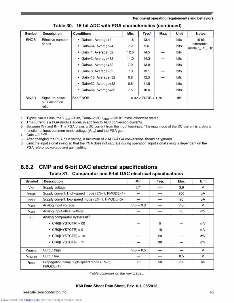
Table 30. 16-bit ADC with PGA characteristics (continued)
Symbol Description Conditions Min. Typ.1 Max. Unit Notes
ENOB Effective numberof bits
• Gain=1, Average=4
• Gain=64, Average=4
• Gain=1, Average=32
• Gain=2, Average=32
• Gain=4, Average=32
• Gain=8, Average=32
• Gain=16, Average=32
• Gain=32, Average=32
• Gain=64, Average=32
11.6
7.2
12.8
11.0
7.9
7.3
6.8
6.8
7.5
13.4
9.6
14.5
14.3
13.8
13.1
12.5
11.5
10.6
—
—
—
—
—
—
—
—
—
bits
bits
bits
bits
bits
bits
bits
bits
bits
16-bitdifferential
mode,fin=100Hz
SINAD Signal-to-noiseplus distortionratio
See ENOB 6.02 × ENOB + 1.76 dB
1. Typical values assume VDDA =3.0V, Temp=25°C, fADCK=6MHz unless otherwise stated.2. This current is a PGA module adder, in addition to ADC conversion currents.3. Between IN+ and IN-. The PGA draws a DC current from the input terminals. The magnitude of the DC current is a strong
function of input common mode voltage (VCM) and the PGA gain.4. Gain = 2PGAG
5. After changing the PGA gain setting, a minimum of 2 ADC+PGA conversions should be ignored.6. Limit the input signal swing so that the PGA does not saturate during operation. Input signal swing is dependent on the
PGA reference voltage and gain setting.
6.6.2 CMP and 6-bit DAC electrical specificationsTable 31. Comparator and 6-bit DAC electrical specifications
Symbol Description Min. Typ. Max. Unit
VDD Supply voltage 1.71 — 3.6 V
IDDHS Supply current, High-speed mode (EN=1, PMODE=1) — — 200 μA
IDDLS Supply current, low-speed mode (EN=1, PMODE=0) — — 20 μA
VAIN Analog input voltage VSS – 0.3 — VDD V
VAIO Analog input offset voltage — — 20 mV
VH Analog comparator hysteresis1
• CR0[HYSTCTR] = 00
• CR0[HYSTCTR] = 01
• CR0[HYSTCTR] = 10
• CR0[HYSTCTR] = 11
—
—
—
—
5
10
20
30
—
—
—
—
mV
mV
mV
mV
VCMPOh Output high VDD – 0.5 — — V
VCMPOl Output low — — 0.5 V
tDHS Propagation delay, high-speed mode (EN=1,PMODE=1)
20 50 200 ns
Table continues on the next page...
Peripheral operating requirements and behaviors
K60 Data Sheet Data Sheet, Rev. 6.1, 08/2012.
Freescale Semiconductor, Inc. 45
Downloaded from Elcodis.com electronic components distributor
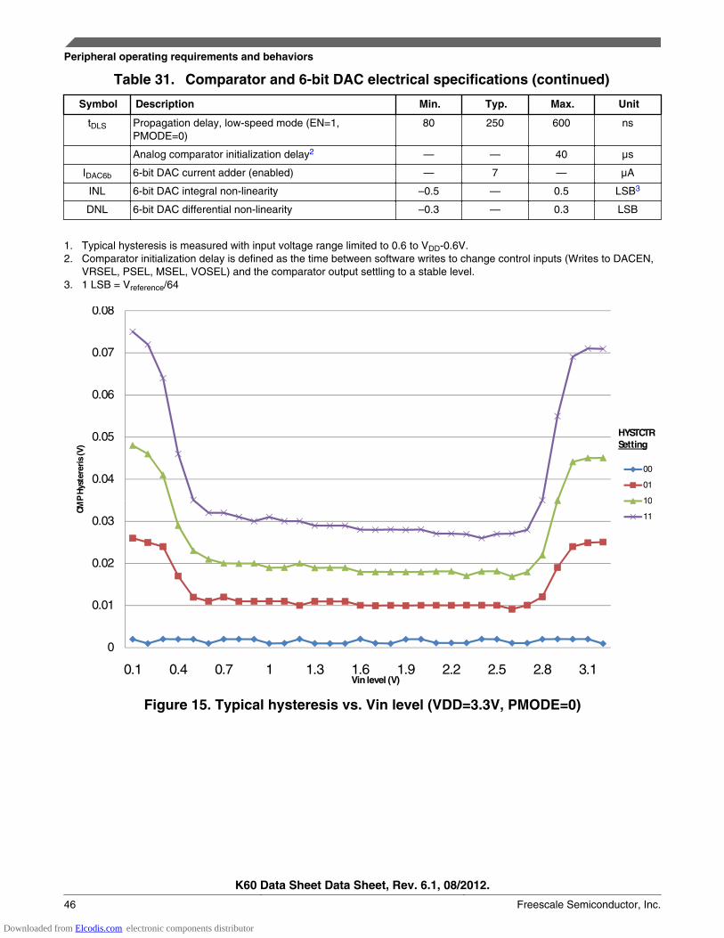
Table 31. Comparator and 6-bit DAC electrical specifications (continued)
Symbol Description Min. Typ. Max. Unit
tDLS Propagation delay, low-speed mode (EN=1,PMODE=0)
80 250 600 ns
Analog comparator initialization delay2 — — 40 μs
IDAC6b 6-bit DAC current adder (enabled) — 7 — μA
INL 6-bit DAC integral non-linearity –0.5 — 0.5 LSB3
DNL 6-bit DAC differential non-linearity –0.3 — 0.3 LSB
1. Typical hysteresis is measured with input voltage range limited to 0.6 to VDD-0.6V.2. Comparator initialization delay is defined as the time between software writes to change control inputs (Writes to DACEN,
VRSEL, PSEL, MSEL, VOSEL) and the comparator output settling to a stable level.3. 1 LSB = Vreference/64
0.04
0.05
0.06
0.07
0.08
P H
yste
reri
s (V
)
00
01
10
HYSTCTR Setting
0
0.01
0.02
0.03
0.1 0.4 0.7 1 1.3 1.6 1.9 2.2 2.5 2.8 3.1
CM
10
11
Vin level (V)
Figure 15. Typical hysteresis vs. Vin level (VDD=3.3V, PMODE=0)
Peripheral operating requirements and behaviors
K60 Data Sheet Data Sheet, Rev. 6.1, 08/2012.
46 Freescale Semiconductor, Inc.
Downloaded from Elcodis.com electronic components distributor
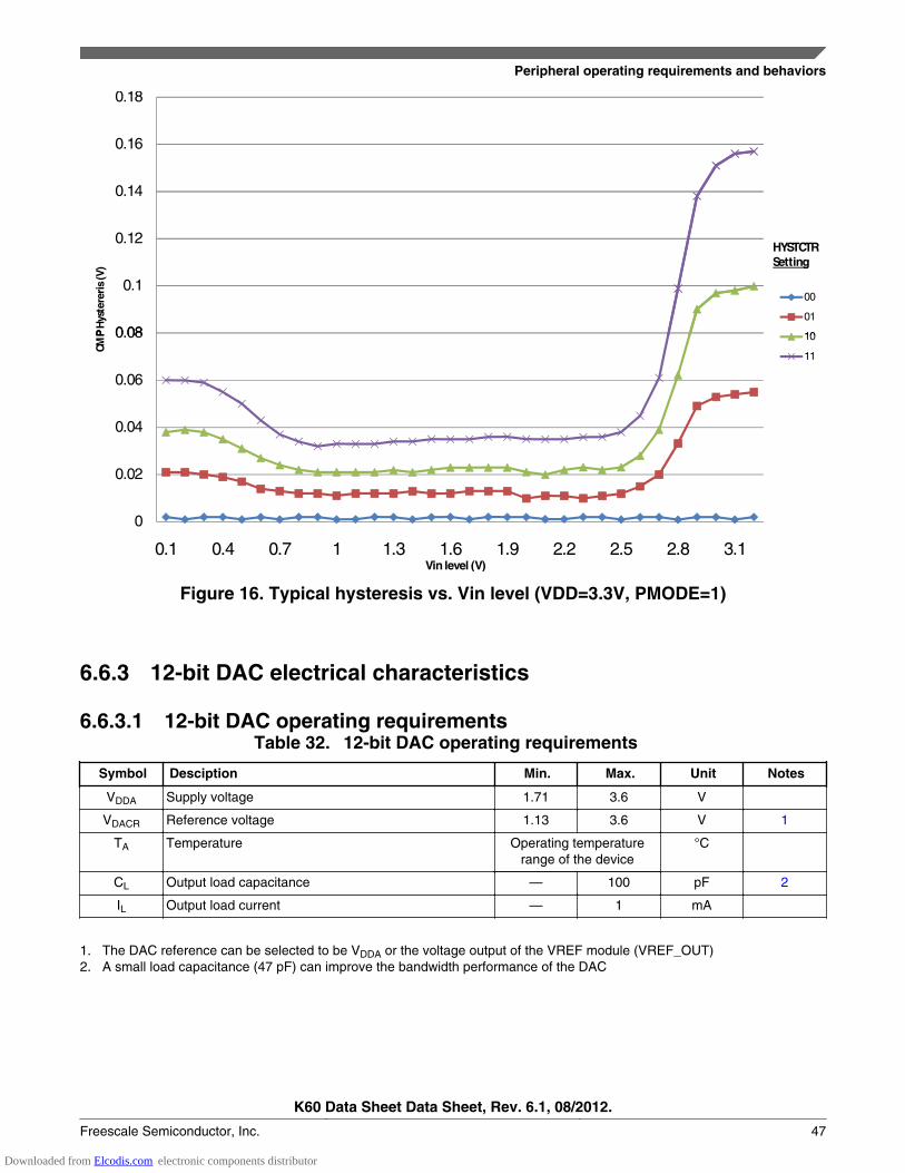
0 08
0.1
0.12
0.14
0.16
0.18P
Hys
tere
ris
(V)
00
01
10
HYSTCTR Setting
0
0.02
0.04
0.06
0.08
0.1 0.4 0.7 1 1.3 1.6 1.9 2.2 2.5 2.8 3.1
CMP 10
11
Vin level (V)
Figure 16. Typical hysteresis vs. Vin level (VDD=3.3V, PMODE=1)
6.6.3 12-bit DAC electrical characteristics
6.6.3.1 12-bit DAC operating requirementsTable 32. 12-bit DAC operating requirements
Symbol Desciption Min. Max. Unit Notes
VDDA Supply voltage 1.71 3.6 V
VDACR Reference voltage 1.13 3.6 V 1
TA Temperature Operating temperaturerange of the device
°C
CL Output load capacitance — 100 pF 2
IL Output load current — 1 mA
1. The DAC reference can be selected to be VDDA or the voltage output of the VREF module (VREF_OUT)2. A small load capacitance (47 pF) can improve the bandwidth performance of the DAC
Peripheral operating requirements and behaviors
K60 Data Sheet Data Sheet, Rev. 6.1, 08/2012.
Freescale Semiconductor, Inc. 47
Downloaded from Elcodis.com electronic components distributor
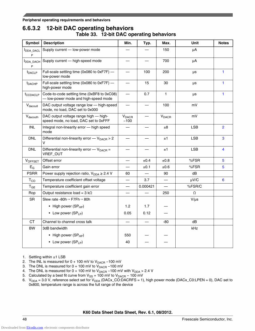
6.6.3.2 12-bit DAC operating behaviorsTable 33. 12-bit DAC operating behaviors
Symbol Description Min. Typ. Max. Unit Notes
IDDA_DACL
P
Supply current — low-power mode — — 150 μA
IDDA_DACH
P
Supply current — high-speed mode — — 700 μA
tDACLP Full-scale settling time (0x080 to 0xF7F) —low-power mode
— 100 200 μs 1
tDACHP Full-scale settling time (0x080 to 0xF7F) —high-power mode
— 15 30 μs 1
tCCDACLP Code-to-code settling time (0xBF8 to 0xC08)— low-power mode and high-speed mode
— 0.7 1 μs 1
Vdacoutl DAC output voltage range low — high-speedmode, no load, DAC set to 0x000
— — 100 mV
Vdacouth DAC output voltage range high — high-speed mode, no load, DAC set to 0xFFF
VDACR−100
— VDACR mV
INL Integral non-linearity error — high speedmode
— — ±8 LSB 2
DNL Differential non-linearity error — VDACR > 2V
— — ±1 LSB 3
DNL Differential non-linearity error — VDACR =VREF_OUT
— — ±1 LSB 4
VOFFSET Offset error — ±0.4 ±0.8 %FSR 5
EG Gain error — ±0.1 ±0.6 %FSR 5
PSRR Power supply rejection ratio, VDDA ≥ 2.4 V 60 — 90 dB
TCO Temperature coefficient offset voltage — 3.7 — μV/C 6
TGE Temperature coefficient gain error — 0.000421 — %FSR/C
Rop Output resistance load = 3 kΩ — — 250 Ω
SR Slew rate -80h→ F7Fh→ 80h
• High power (SPHP)
• Low power (SPLP)
1.2
0.05
1.7
0.12
—
—
V/μs
CT Channel to channel cross talk — — -80 dB
BW 3dB bandwidth
• High power (SPHP)
• Low power (SPLP)
550
40
—
—
—
—
kHz
1. Settling within ±1 LSB2. The INL is measured for 0 + 100 mV to VDACR −100 mV3. The DNL is measured for 0 + 100 mV to VDACR −100 mV4. The DNL is measured for 0 + 100 mV to VDACR −100 mV with VDDA > 2.4 V5. Calculated by a best fit curve from VSS + 100 mV to VDACR − 100 mV6. VDDA = 3.0 V, reference select set for VDDA (DACx_CO:DACRFS = 1), high power mode (DACx_C0:LPEN = 0), DAC set to
0x800, temperature range is across the full range of the device
Peripheral operating requirements and behaviors
K60 Data Sheet Data Sheet, Rev. 6.1, 08/2012.
48 Freescale Semiconductor, Inc.
Downloaded from Elcodis.com electronic components distributor
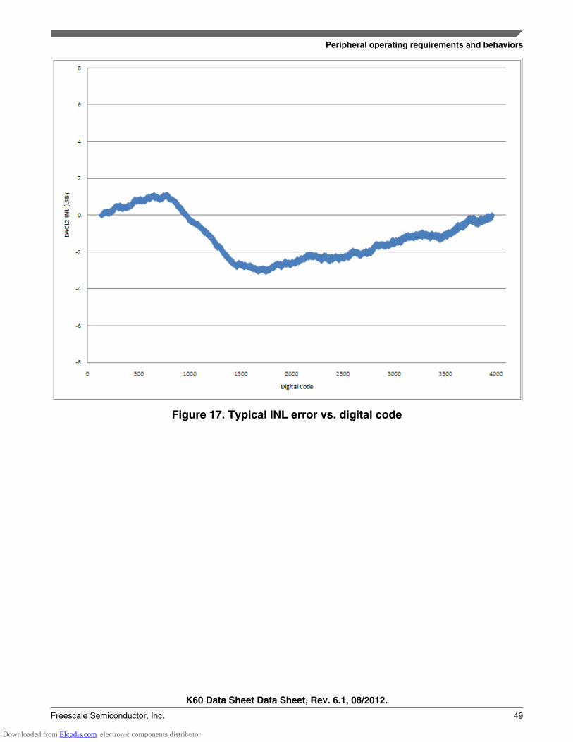
Figure 17. Typical INL error vs. digital code
Peripheral operating requirements and behaviors
K60 Data Sheet Data Sheet, Rev. 6.1, 08/2012.
Freescale Semiconductor, Inc. 49
Downloaded from Elcodis.com electronic components distributor
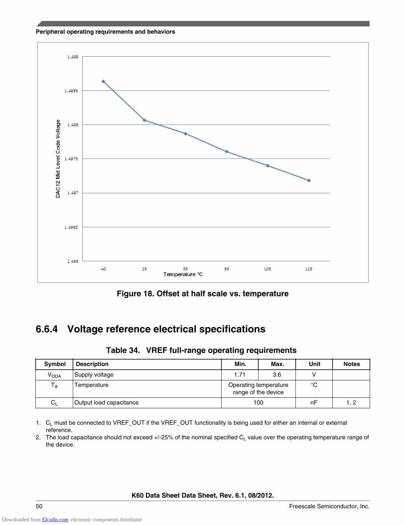
Figure 18. Offset at half scale vs. temperature
6.6.4 Voltage reference electrical specifications
Table 34. VREF full-range operating requirements
Symbol Description Min. Max. Unit Notes
VDDA Supply voltage 1.71 3.6 V
TA Temperature Operating temperaturerange of the device
°C
CL Output load capacitance 100 nF 1, 2
1. CL must be connected to VREF_OUT if the VREF_OUT functionality is being used for either an internal or externalreference.
2. The load capacitance should not exceed +/-25% of the nominal specified CL value over the operating temperature range ofthe device.
Peripheral operating requirements and behaviors
K60 Data Sheet Data Sheet, Rev. 6.1, 08/2012.
50 Freescale Semiconductor, Inc.
Downloaded from Elcodis.com electronic components distributor
Table 35. VREF full-range operating behaviors
Symbol Description Min. Typ. Max. Unit Notes
Vout Voltage reference output with factory trim atnominal VDDA and temperature=25C
1.1915 1.195 1.1977 V
Vout Voltage reference output — factory trim 1.1584 — 1.2376 V
Vstep Voltage reference trim step — 0.5 — mV
Vtdrift Temperature drift (Vmax -Vmin across the fulltemperature range: 0 to 70°C)
— — 50 mV
Vtdrift Temperature drift (Vmax -Vmin across the fulltemperature range: -40 to 85°C)
— — 70 mV
Ibg Bandgap only current — — 80 µA 1
Ilp Low-power buffer current — — 360 uA 1
Ihp High-power buffer current — — 1 mA 1
ΔVLOAD Load regulation
• current = + 1.0 mA
• current = - 1.0 mA
—
—
2
5
—
—
mV 1, 2
Tstup Buffer startup time — — 100 µs
Vvdrift Voltage drift (Vmax -Vmin across the full voltagerange)
— 2 — mV 1
1. See the chip's Reference Manual for the appropriate settings of the VREF Status and Control register.2. Load regulation voltage is the difference between the VREF_OUT voltage with no load vs. voltage with defined load
Table 36. VREF limited-range operating requirements
Symbol Description Min. Max. Unit Notes
TA Temperature 0 50 °C
Table 37. VREF limited-range operating behaviors
Symbol Description Min. Max. Unit Notes
Vout Voltage reference output with factory trim 1.173 1.225 V
6.7 Timers
See General switching specifications.
6.8 Communication interfaces
Peripheral operating requirements and behaviors
K60 Data Sheet Data Sheet, Rev. 6.1, 08/2012.
Freescale Semiconductor, Inc. 51
Downloaded from Elcodis.com electronic components distributor
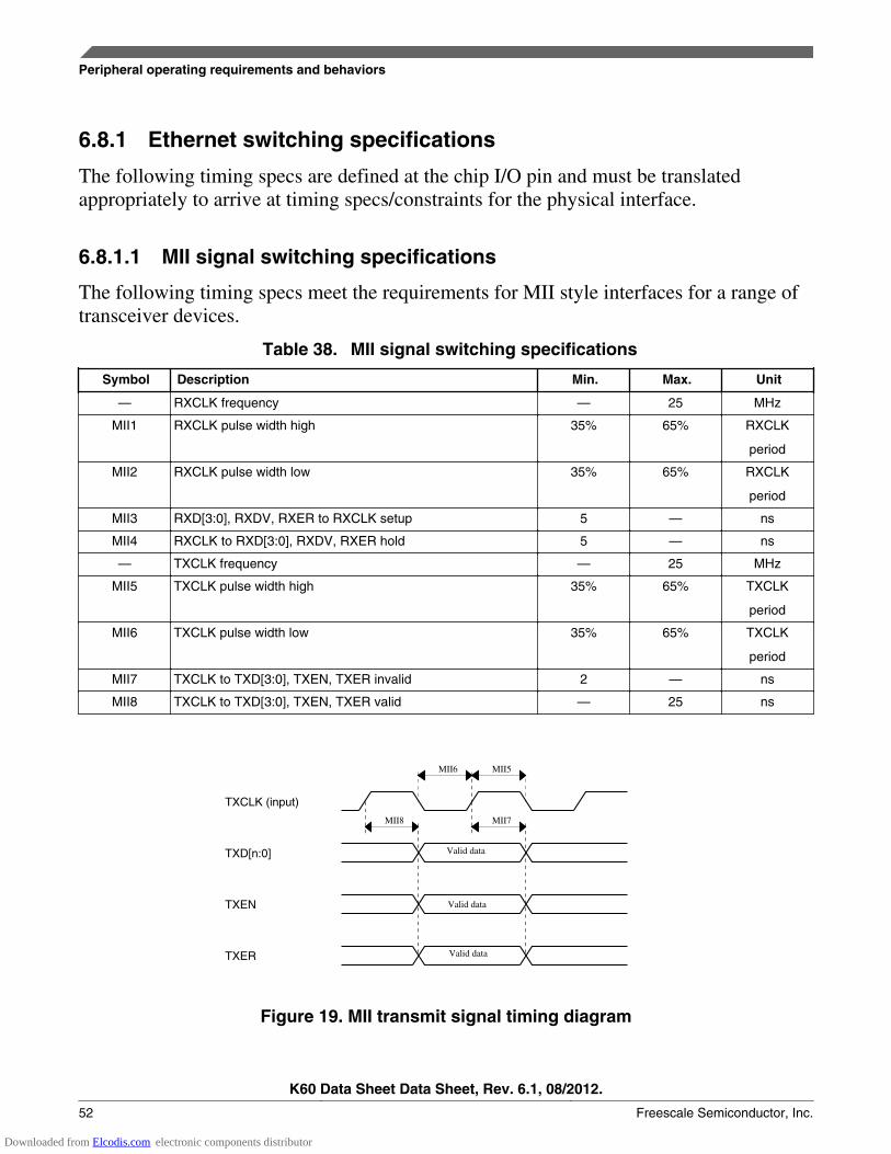
6.8.1 Ethernet switching specifications
The following timing specs are defined at the chip I/O pin and must be translatedappropriately to arrive at timing specs/constraints for the physical interface.
6.8.1.1 MII signal switching specifications
The following timing specs meet the requirements for MII style interfaces for a range oftransceiver devices.
Table 38. MII signal switching specifications
Symbol Description Min. Max. Unit
— RXCLK frequency — 25 MHz
MII1 RXCLK pulse width high 35% 65% RXCLK
period
MII2 RXCLK pulse width low 35% 65% RXCLK
period
MII3 RXD[3:0], RXDV, RXER to RXCLK setup 5 — ns
MII4 RXCLK to RXD[3:0], RXDV, RXER hold 5 — ns
— TXCLK frequency — 25 MHz
MII5 TXCLK pulse width high 35% 65% TXCLK
period
MII6 TXCLK pulse width low 35% 65% TXCLK
period
MII7 TXCLK to TXD[3:0], TXEN, TXER invalid 2 — ns
MII8 TXCLK to TXD[3:0], TXEN, TXER valid — 25 ns
MII7MII8
Valid data
Valid data
Valid data
MII6 MII5
TXCLK (input)
TXD[n:0]
TXEN
TXER
Figure 19. MII transmit signal timing diagram
Peripheral operating requirements and behaviors
K60 Data Sheet Data Sheet, Rev. 6.1, 08/2012.
52 Freescale Semiconductor, Inc.
Downloaded from Elcodis.com electronic components distributor
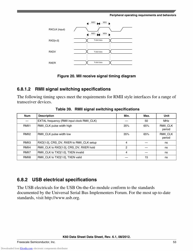
MII2 MII1
MII4MII3
Valid data
Valid data
Valid data
RXCLK (input)
RXD[n:0]
RXDV
RXER
Figure 20. MII receive signal timing diagram
6.8.1.2 RMII signal switching specifications
The following timing specs meet the requirements for RMII style interfaces for a range oftransceiver devices.
Table 39. RMII signal switching specifications
Num Description Min. Max. Unit
— EXTAL frequency (RMII input clock RMII_CLK) — 50 MHz
RMII1 RMII_CLK pulse width high 35% 65% RMII_CLKperiod
RMII2 RMII_CLK pulse width low 35% 65% RMII_CLKperiod
RMII3 RXD[1:0], CRS_DV, RXER to RMII_CLK setup 4 — ns
RMII4 RMII_CLK to RXD[1:0], CRS_DV, RXER hold 2 — ns
RMII7 RMII_CLK to TXD[1:0], TXEN invalid 4 — ns
RMII8 RMII_CLK to TXD[1:0], TXEN valid — 15 ns
6.8.2 USB electrical specifications
The USB electricals for the USB On-the-Go module conform to the standardsdocumented by the Universal Serial Bus Implementers Forum. For the most up-to-datestandards, visit http://www.usb.org.
Peripheral operating requirements and behaviors
K60 Data Sheet Data Sheet, Rev. 6.1, 08/2012.
Freescale Semiconductor, Inc. 53
Downloaded from Elcodis.com electronic components distributor
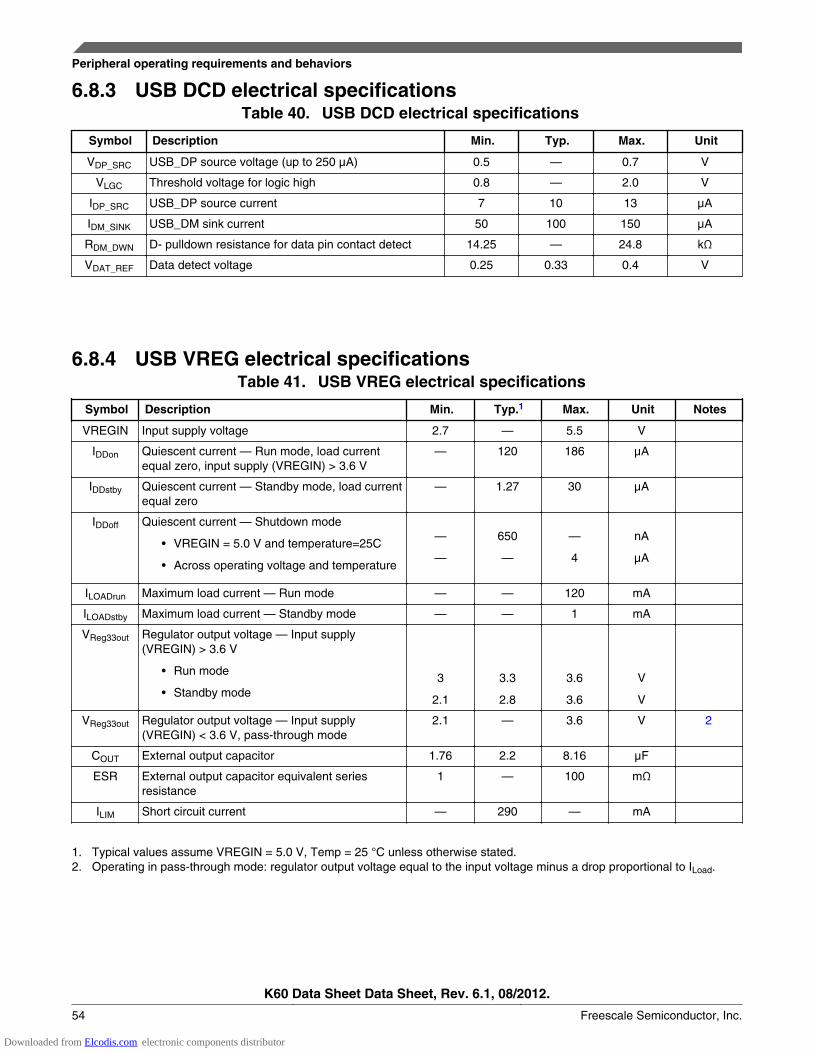
6.8.3 USB DCD electrical specificationsTable 40. USB DCD electrical specifications
Symbol Description Min. Typ. Max. Unit
VDP_SRC USB_DP source voltage (up to 250 μA) 0.5 — 0.7 V
VLGC Threshold voltage for logic high 0.8 — 2.0 V
IDP_SRC USB_DP source current 7 10 13 μA
IDM_SINK USB_DM sink current 50 100 150 μA
RDM_DWN D- pulldown resistance for data pin contact detect 14.25 — 24.8 kΩ
VDAT_REF Data detect voltage 0.25 0.33 0.4 V
6.8.4 USB VREG electrical specificationsTable 41. USB VREG electrical specifications
Symbol Description Min. Typ.1 Max. Unit Notes
VREGIN Input supply voltage 2.7 — 5.5 V
IDDon Quiescent current — Run mode, load currentequal zero, input supply (VREGIN) > 3.6 V
— 120 186 μA
IDDstby Quiescent current — Standby mode, load currentequal zero
— 1.27 30 μA
IDDoff Quiescent current — Shutdown mode
• VREGIN = 5.0 V and temperature=25C
• Across operating voltage and temperature
—
—
650
—
—
4
nA
μA
ILOADrun Maximum load current — Run mode — — 120 mA
ILOADstby Maximum load current — Standby mode — — 1 mA
VReg33out Regulator output voltage — Input supply(VREGIN) > 3.6 V
• Run mode
• Standby mode
3
2.1
3.3
2.8
3.6
3.6
V
V
VReg33out Regulator output voltage — Input supply(VREGIN) < 3.6 V, pass-through mode
2.1 — 3.6 V 2
COUT External output capacitor 1.76 2.2 8.16 μF
ESR External output capacitor equivalent seriesresistance
1 — 100 mΩ
ILIM Short circuit current — 290 — mA
1. Typical values assume VREGIN = 5.0 V, Temp = 25 °C unless otherwise stated.2. Operating in pass-through mode: regulator output voltage equal to the input voltage minus a drop proportional to ILoad.
Peripheral operating requirements and behaviors
K60 Data Sheet Data Sheet, Rev. 6.1, 08/2012.
54 Freescale Semiconductor, Inc.
Downloaded from Elcodis.com electronic components distributor
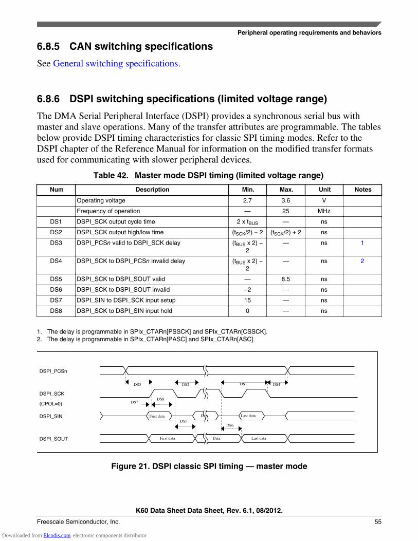
6.8.5 CAN switching specifications
See General switching specifications.
6.8.6 DSPI switching specifications (limited voltage range)
The DMA Serial Peripheral Interface (DSPI) provides a synchronous serial bus withmaster and slave operations. Many of the transfer attributes are programmable. The tablesbelow provide DSPI timing characteristics for classic SPI timing modes. Refer to theDSPI chapter of the Reference Manual for information on the modified transfer formatsused for communicating with slower peripheral devices.
Table 42. Master mode DSPI timing (limited voltage range)
Num Description Min. Max. Unit Notes
Operating voltage 2.7 3.6 V
Frequency of operation — 25 MHz
DS1 DSPI_SCK output cycle time 2 x tBUS — ns
DS2 DSPI_SCK output high/low time (tSCK/2) − 2 (tSCK/2) + 2 ns
DS3 DSPI_PCSn valid to DSPI_SCK delay (tBUS x 2) −2
— ns 1
DS4 DSPI_SCK to DSPI_PCSn invalid delay (tBUS x 2) −2
— ns 2
DS5 DSPI_SCK to DSPI_SOUT valid — 8.5 ns
DS6 DSPI_SCK to DSPI_SOUT invalid −2 — ns
DS7 DSPI_SIN to DSPI_SCK input setup 15 — ns
DS8 DSPI_SCK to DSPI_SIN input hold 0 — ns
1. The delay is programmable in SPIx_CTARn[PSSCK] and SPIx_CTARn[CSSCK].2. The delay is programmable in SPIx_CTARn[PASC] and SPIx_CTARn[ASC].
DS3 DS4DS1DS2
DS7DS8
First data Last dataDS5
First data Data Last data
DS6
Data
DSPI_PCSn
DSPI_SCK
(CPOL=0)
DSPI_SIN
DSPI_SOUT
Figure 21. DSPI classic SPI timing — master mode
Peripheral operating requirements and behaviors
K60 Data Sheet Data Sheet, Rev. 6.1, 08/2012.
Freescale Semiconductor, Inc. 55
Downloaded from Elcodis.com electronic components distributor
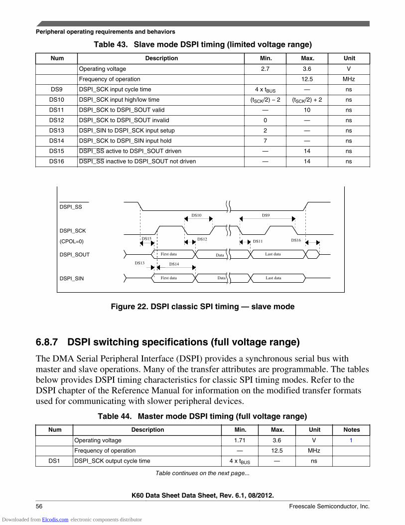
Table 43. Slave mode DSPI timing (limited voltage range)
Num Description Min. Max. Unit
Operating voltage 2.7 3.6 V
Frequency of operation 12.5 MHz
DS9 DSPI_SCK input cycle time 4 x tBUS — ns
DS10 DSPI_SCK input high/low time (tSCK/2) − 2 (tSCK/2) + 2 ns
DS11 DSPI_SCK to DSPI_SOUT valid — 10 ns
DS12 DSPI_SCK to DSPI_SOUT invalid 0 — ns
DS13 DSPI_SIN to DSPI_SCK input setup 2 — ns
DS14 DSPI_SCK to DSPI_SIN input hold 7 — ns
DS15 DSPI_SS active to DSPI_SOUT driven — 14 ns
DS16 DSPI_SS inactive to DSPI_SOUT not driven — 14 ns
First data Last data
First data Data Last data
Data
DS15
DS10 DS9
DS16DS11DS12
DS14DS13
DSPI_SS
DSPI_SCK
(CPOL=0)
DSPI_SOUT
DSPI_SIN
Figure 22. DSPI classic SPI timing — slave mode
6.8.7 DSPI switching specifications (full voltage range)
The DMA Serial Peripheral Interface (DSPI) provides a synchronous serial bus withmaster and slave operations. Many of the transfer attributes are programmable. The tablesbelow provides DSPI timing characteristics for classic SPI timing modes. Refer to theDSPI chapter of the Reference Manual for information on the modified transfer formatsused for communicating with slower peripheral devices.
Table 44. Master mode DSPI timing (full voltage range)
Num Description Min. Max. Unit Notes
Operating voltage 1.71 3.6 V 1
Frequency of operation — 12.5 MHz
DS1 DSPI_SCK output cycle time 4 x tBUS — ns
Table continues on the next page...
Peripheral operating requirements and behaviors
K60 Data Sheet Data Sheet, Rev. 6.1, 08/2012.
56 Freescale Semiconductor, Inc.
Downloaded from Elcodis.com electronic components distributor
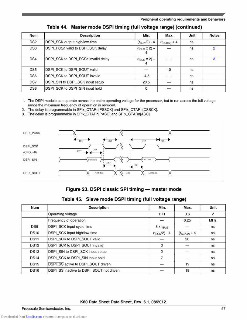
Table 44. Master mode DSPI timing (full voltage range) (continued)
Num Description Min. Max. Unit Notes
DS2 DSPI_SCK output high/low time (tSCK/2) - 4 (tSCK/2) + 4 ns
DS3 DSPI_PCSn valid to DSPI_SCK delay (tBUS x 2) −4
— ns 2
DS4 DSPI_SCK to DSPI_PCSn invalid delay (tBUS x 2) −4
— ns 3
DS5 DSPI_SCK to DSPI_SOUT valid — 10 ns
DS6 DSPI_SCK to DSPI_SOUT invalid -4.5 — ns
DS7 DSPI_SIN to DSPI_SCK input setup 20.5 — ns
DS8 DSPI_SCK to DSPI_SIN input hold 0 — ns
1. The DSPI module can operate across the entire operating voltage for the processor, but to run across the full voltagerange the maximum frequency of operation is reduced.
2. The delay is programmable in SPIx_CTARn[PSSCK] and SPIx_CTARn[CSSCK].3. The delay is programmable in SPIx_CTARn[PASC] and SPIx_CTARn[ASC].
DS3 DS4DS1DS2
DS7DS8
First data Last dataDS5
First data Data Last data
DS6
Data
DSPI_PCSn
DSPI_SCK
(CPOL=0)
DSPI_SIN
DSPI_SOUT
Figure 23. DSPI classic SPI timing — master mode
Table 45. Slave mode DSPI timing (full voltage range)
Num Description Min. Max. Unit
Operating voltage 1.71 3.6 V
Frequency of operation — 6.25 MHz
DS9 DSPI_SCK input cycle time 8 x tBUS — ns
DS10 DSPI_SCK input high/low time (tSCK/2) - 4 (tSCK/2) + 4 ns
DS11 DSPI_SCK to DSPI_SOUT valid — 20 ns
DS12 DSPI_SCK to DSPI_SOUT invalid 0 — ns
DS13 DSPI_SIN to DSPI_SCK input setup 2 — ns
DS14 DSPI_SCK to DSPI_SIN input hold 7 — ns
DS15 DSPI_SS active to DSPI_SOUT driven — 19 ns
DS16 DSPI_SS inactive to DSPI_SOUT not driven — 19 ns
Peripheral operating requirements and behaviors
K60 Data Sheet Data Sheet, Rev. 6.1, 08/2012.
Freescale Semiconductor, Inc. 57
Downloaded from Elcodis.com electronic components distributor
First data Last data
First data Data Last data
Data
DS15
DS10 DS9
DS16DS11DS12
DS14DS13
DSPI_SS
DSPI_SCK
(CPOL=0)
DSPI_SOUT
DSPI_SIN
Figure 24. DSPI classic SPI timing — slave mode
6.8.8 I2C switching specifications
See General switching specifications.
6.8.9 UART switching specifications
See General switching specifications.
6.8.10 SDHC specifications
The following timing specs are defined at the chip I/O pin and must be translatedappropriately to arrive at timing specs/constraints for the physical interface.
Table 46. SDHC switching specifications
Num Symbol Description Min. Max. Unit
Card input clock
SD1 fpp Clock frequency (low speed) 0 400 kHz
fpp Clock frequency (SD\SDIO full speed) 0 25 MHz
fpp Clock frequency (MMC full speed) 0 20 MHz
fOD Clock frequency (identification mode) 0 400 kHz
SD2 tWL Clock low time 7 — ns
SD3 tWH Clock high time 7 — ns
SD4 tTLH Clock rise time Refer Table 3 ns
SD5 tTHL Clock fall time ns
SDHC output / card inputs SDHC_CMD, SDHC_DAT (reference to SDHC_CLK)
Table continues on the next page...
Peripheral operating requirements and behaviors
K60 Data Sheet Data Sheet, Rev. 6.1, 08/2012.
58 Freescale Semiconductor, Inc.
Downloaded from Elcodis.com electronic components distributor
Table 46. SDHC switching specifications(continued)
Num Symbol Description Min. Max. Unit
SD6 tOD SDHC output delay (output valid) -5 6.5 ns
SDHC input / card inputs SDHC_CMD, SDHC_DAT (reference to SDHC_CLK)
SD7 tISU SDHC input setup time 5 — ns
SD8 tIH SDHC input hold time 0 — ns
SD2SD3 SD1
SD6
SD8SD7
SDHC_CLK
Output SDHC_CMD
Output SDHC_DAT[3:0]
Input SDHC_CMD
Input SDHC_DAT[3:0]
Figure 25. SDHC timing
6.8.11 I2S switching specifications
This section provides the AC timings for the I2S in master (clocks driven) and slavemodes (clocks input). All timings are given for non-inverted serial clock polarity(TCR[TSCKP] = 0, RCR[RSCKP] = 0) and a non-inverted frame sync (TCR[TFSI] = 0,RCR[RFSI] = 0). If the polarity of the clock and/or the frame sync have been inverted, allthe timings remain valid by inverting the clock signal (I2S_BCLK) and/or the frame sync(I2S_FS) shown in the figures below.
Table 47. I2S master mode timing
Num Description Min. Max. Unit
Operating voltage 2.7 3.6 V
S1 I2S_MCLK cycle time 2 x tSYS ns
S2 I2S_MCLK pulse width high/low 45% 55% MCLK period
S3 I2S_BCLK cycle time 5 x tSYS — ns
S4 I2S_BCLK pulse width high/low 45% 55% BCLK period
S5 I2S_BCLK to I2S_FS output valid — 15 ns
Table continues on the next page...
Peripheral operating requirements and behaviors
K60 Data Sheet Data Sheet, Rev. 6.1, 08/2012.
Freescale Semiconductor, Inc. 59
Downloaded from Elcodis.com electronic components distributor
Table 47. I2S master mode timing (continued)
Num Description Min. Max. Unit
S6 I2S_BCLK to I2S_FS output invalid -2.5 — ns
S7 I2S_BCLK to I2S_TXD valid — 15 ns
S8 I2S_BCLK to I2S_TXD invalid -3 — ns
S9 I2S_RXD/I2S_FS input setup before I2S_BCLK 20 — ns
S10 I2S_RXD/I2S_FS input hold after I2S_BCLK 0 — ns
S1 S2 S2
S3
S4
S4
S5
S9
S7
S9 S10
S7
S8
S6
S10
S8
I2S_MCLK (output)
I2S_BCLK (output)
I2S_FS (output)
I2S_FS (input)
I2S_TXD
I2S_RXD
Figure 26. I2S timing — master mode
Table 48. I2S slave mode timing
Num Description Min. Max. Unit
Operating voltage 2.7 3.6 V
S11 I2S_BCLK cycle time (input) 8 x tSYS — ns
S12 I2S_BCLK pulse width high/low (input) 45% 55% MCLK period
S13 I2S_FS input setup before I2S_BCLK 10 — ns
S14 I2S_FS input hold after I2S_BCLK 3 — ns
S15 I2S_BCLK to I2S_TXD/I2S_FS output valid — 20 ns
S16 I2S_BCLK to I2S_TXD/I2S_FS output invalid 0 — ns
S17 I2S_RXD setup before I2S_BCLK 10 — ns
S18 I2S_RXD hold after I2S_BCLK 2 — ns
Peripheral operating requirements and behaviors
K60 Data Sheet Data Sheet, Rev. 6.1, 08/2012.
60 Freescale Semiconductor, Inc.
Downloaded from Elcodis.com electronic components distributor
S15
S13
S15
S17 S18
S15
S16
S16
S14
S16
S11
S12
S12
I2S_BCLK (input)
I2S_FS (output)
I2S_FS (input)
I2S_TXD
I2S_RXD
Figure 27. I2S timing — slave modes
6.9 Human-machine interfaces (HMI)
6.9.1 TSI electrical specificationsTable 49. TSI electrical specifications
Symbol Description Min. Typ. Max. Unit Notes
VDDTSI Operating voltage 1.71 — 3.6 V
CELE Target electrode capacitance range 1 20 500 pF 1
fREFmax Reference oscillator frequency — 5.5 12.7 MHz 2
fELEmax Electrode oscillator frequency — 0.5 4.0 MHz 3
CREF Internal reference capacitor 0.5 1 1.2 pF
VDELTA Oscillator delta voltage 100 600 760 mV 4
IREF Reference oscillator current source base current• 1uA setting (REFCHRG=0)• 32uA setting (REFCHRG=31)
—
—
1.133
36
1.5
50
μA 3 , 5
IELE Electrode oscillator current source base current• 1uA setting (EXTCHRG=0)• 32uA setting (EXTCHRG=31)
—
—
1.133
36
1.5
50
μA 3 , 6
Pres5 Electrode capacitance measurement precision — 8.3333 38400 fF/count 7
Pres20 Electrode capacitance measurement precision — 8.3333 38400 fF/count 8
Pres100 Electrode capacitance measurement precision — 8.3333 38400 fF/count 9
MaxSens Maximum sensitivity 0.003 12.5 — fF/count 10
Res Resolution — — 16 bits
TCon20 Response time @ 20 pF 8 15 25 μs 11
ITSI_RUN Current added in run mode — 55 — μA
ITSI_LP Low power mode current adder — 1.3 2.5 μA 12
Peripheral operating requirements and behaviors
K60 Data Sheet Data Sheet, Rev. 6.1, 08/2012.
Freescale Semiconductor, Inc. 61
Downloaded from Elcodis.com electronic components distributor
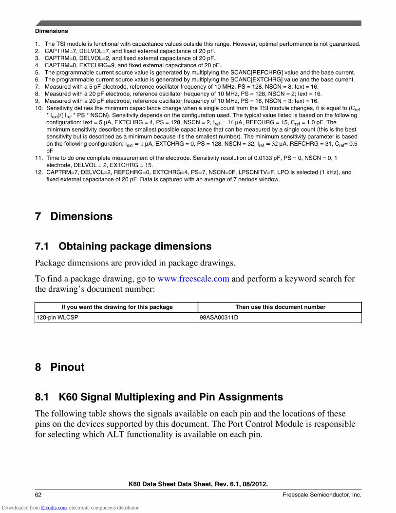
1. The TSI module is functional with capacitance values outside this range. However, optimal performance is not guaranteed.2. CAPTRM=7, DELVOL=7, and fixed external capacitance of 20 pF.3. CAPTRM=0, DELVOL=2, and fixed external capacitance of 20 pF.4. CAPTRM=0, EXTCHRG=9, and fixed external capacitance of 20 pF.5. The programmable current source value is generated by multiplying the SCANC[REFCHRG] value and the base current.6. The programmable current source value is generated by multiplying the SCANC[EXTCHRG] value and the base current.7. Measured with a 5 pF electrode, reference oscillator frequency of 10 MHz, PS = 128, NSCN = 8; Iext = 16.8. Measured with a 20 pF electrode, reference oscillator frequency of 10 MHz, PS = 128, NSCN = 2; Iext = 16.9. Measured with a 20 pF electrode, reference oscillator frequency of 10 MHz, PS = 16, NSCN = 3; Iext = 16.10. Sensitivity defines the minimum capacitance change when a single count from the TSI module changes, it is equal to (Cref
* Iext)/( Iref * PS * NSCN). Sensitivity depends on the configuration used. The typical value listed is based on the followingconfiguration: Iext = 5 μA, EXTCHRG = 4, PS = 128, NSCN = 2, Iref = 16 μA, REFCHRG = 15, Cref = 1.0 pF. Theminimum sensitivity describes the smallest possible capacitance that can be measured by a single count (this is the bestsensitivity but is described as a minimum because it’s the smallest number). The minimum sensitivity parameter is basedon the following configuration: Iext = 1 μA, EXTCHRG = 0, PS = 128, NSCN = 32, Iref = 32 μA, REFCHRG = 31, Cref= 0.5pF
11. Time to do one complete measurement of the electrode. Sensitivity resolution of 0.0133 pF, PS = 0, NSCN = 0, 1electrode, DELVOL = 2, EXTCHRG = 15.
12. CAPTRM=7, DELVOL=2, REFCHRG=0, EXTCHRG=4, PS=7, NSCN=0F, LPSCNITV=F, LPO is selected (1 kHz), andfixed external capacitance of 20 pF. Data is captured with an average of 7 periods window.
7 Dimensions
7.1 Obtaining package dimensions
Package dimensions are provided in package drawings.
To find a package drawing, go to www.freescale.com and perform a keyword search forthe drawing’s document number:
If you want the drawing for this package Then use this document number
120-pin WLCSP 98ASA00311D
8 Pinout
8.1 K60 Signal Multiplexing and Pin Assignments
The following table shows the signals available on each pin and the locations of thesepins on the devices supported by this document. The Port Control Module is responsiblefor selecting which ALT functionality is available on each pin.
Dimensions
K60 Data Sheet Data Sheet, Rev. 6.1, 08/2012.
62 Freescale Semiconductor, Inc.
Downloaded from Elcodis.com electronic components distributor
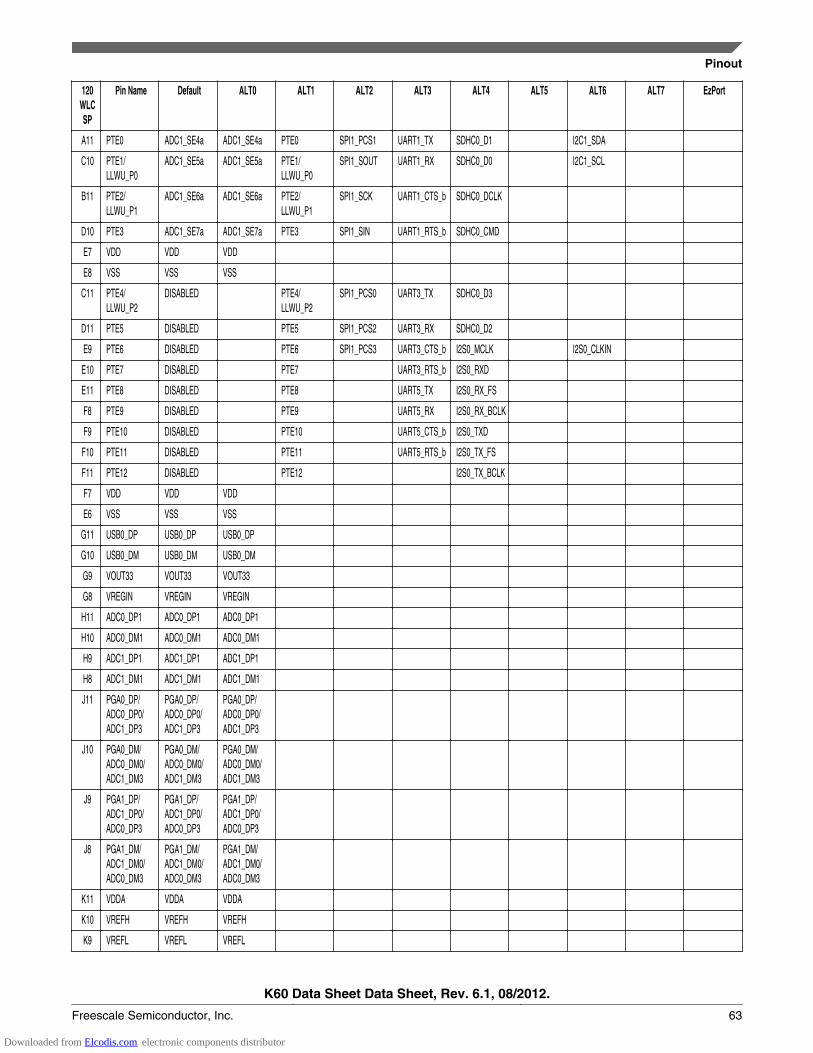
120WLCSP
Pin Name Default ALT0 ALT1 ALT2 ALT3 ALT4 ALT5 ALT6 ALT7 EzPort
A11 PTE0 ADC1_SE4a ADC1_SE4a PTE0 SPI1_PCS1 UART1_TX SDHC0_D1 I2C1_SDA
C10 PTE1/LLWU_P0
ADC1_SE5a ADC1_SE5a PTE1/LLWU_P0
SPI1_SOUT UART1_RX SDHC0_D0 I2C1_SCL
B11 PTE2/LLWU_P1
ADC1_SE6a ADC1_SE6a PTE2/LLWU_P1
SPI1_SCK UART1_CTS_b SDHC0_DCLK
D10 PTE3 ADC1_SE7a ADC1_SE7a PTE3 SPI1_SIN UART1_RTS_b SDHC0_CMD
E7 VDD VDD VDD
E8 VSS VSS VSS
C11 PTE4/LLWU_P2
DISABLED PTE4/LLWU_P2
SPI1_PCS0 UART3_TX SDHC0_D3
D11 PTE5 DISABLED PTE5 SPI1_PCS2 UART3_RX SDHC0_D2
E9 PTE6 DISABLED PTE6 SPI1_PCS3 UART3_CTS_b I2S0_MCLK I2S0_CLKIN
E10 PTE7 DISABLED PTE7 UART3_RTS_b I2S0_RXD
E11 PTE8 DISABLED PTE8 UART5_TX I2S0_RX_FS
F8 PTE9 DISABLED PTE9 UART5_RX I2S0_RX_BCLK
F9 PTE10 DISABLED PTE10 UART5_CTS_b I2S0_TXD
F10 PTE11 DISABLED PTE11 UART5_RTS_b I2S0_TX_FS
F11 PTE12 DISABLED PTE12 I2S0_TX_BCLK
F7 VDD VDD VDD
E6 VSS VSS VSS
G11 USB0_DP USB0_DP USB0_DP
G10 USB0_DM USB0_DM USB0_DM
G9 VOUT33 VOUT33 VOUT33
G8 VREGIN VREGIN VREGIN
H11 ADC0_DP1 ADC0_DP1 ADC0_DP1
H10 ADC0_DM1 ADC0_DM1 ADC0_DM1
H9 ADC1_DP1 ADC1_DP1 ADC1_DP1
H8 ADC1_DM1 ADC1_DM1 ADC1_DM1
J11 PGA0_DP/ADC0_DP0/ADC1_DP3
PGA0_DP/ADC0_DP0/ADC1_DP3
PGA0_DP/ADC0_DP0/ADC1_DP3
J10 PGA0_DM/ADC0_DM0/ADC1_DM3
PGA0_DM/ADC0_DM0/ADC1_DM3
PGA0_DM/ADC0_DM0/ADC1_DM3
J9 PGA1_DP/ADC1_DP0/ADC0_DP3
PGA1_DP/ADC1_DP0/ADC0_DP3
PGA1_DP/ADC1_DP0/ADC0_DP3
J8 PGA1_DM/ADC1_DM0/ADC0_DM3
PGA1_DM/ADC1_DM0/ADC0_DM3
PGA1_DM/ADC1_DM0/ADC0_DM3
K11 VDDA VDDA VDDA
K10 VREFH VREFH VREFH
K9 VREFL VREFL VREFL
Pinout
K60 Data Sheet Data Sheet, Rev. 6.1, 08/2012.
Freescale Semiconductor, Inc. 63
Downloaded from Elcodis.com electronic components distributor
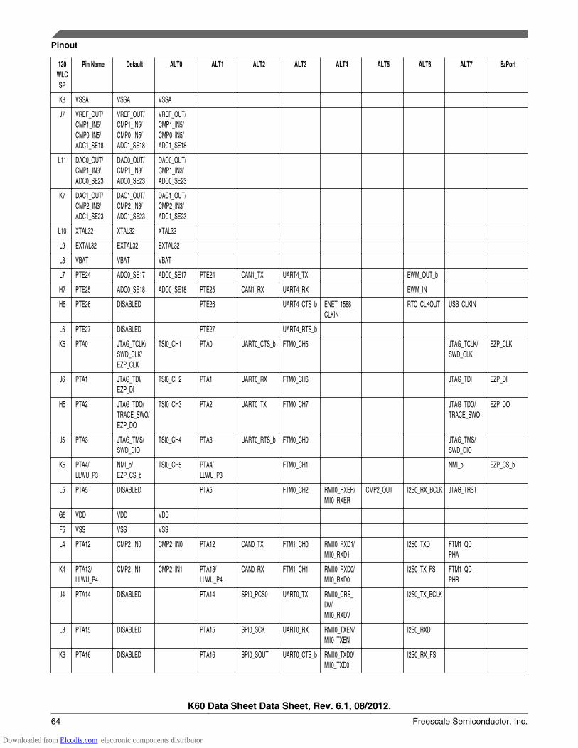
120WLCSP
Pin Name Default ALT0 ALT1 ALT2 ALT3 ALT4 ALT5 ALT6 ALT7 EzPort
K8 VSSA VSSA VSSA
J7 VREF_OUT/CMP1_IN5/CMP0_IN5/ADC1_SE18
VREF_OUT/CMP1_IN5/CMP0_IN5/ADC1_SE18
VREF_OUT/CMP1_IN5/CMP0_IN5/ADC1_SE18
L11 DAC0_OUT/CMP1_IN3/ADC0_SE23
DAC0_OUT/CMP1_IN3/ADC0_SE23
DAC0_OUT/CMP1_IN3/ADC0_SE23
K7 DAC1_OUT/CMP2_IN3/ADC1_SE23
DAC1_OUT/CMP2_IN3/ADC1_SE23
DAC1_OUT/CMP2_IN3/ADC1_SE23
L10 XTAL32 XTAL32 XTAL32
L9 EXTAL32 EXTAL32 EXTAL32
L8 VBAT VBAT VBAT
L7 PTE24 ADC0_SE17 ADC0_SE17 PTE24 CAN1_TX UART4_TX EWM_OUT_b
H7 PTE25 ADC0_SE18 ADC0_SE18 PTE25 CAN1_RX UART4_RX EWM_IN
H6 PTE26 DISABLED PTE26 UART4_CTS_b ENET_1588_CLKIN
RTC_CLKOUT USB_CLKIN
L6 PTE27 DISABLED PTE27 UART4_RTS_b
K6 PTA0 JTAG_TCLK/SWD_CLK/EZP_CLK
TSI0_CH1 PTA0 UART0_CTS_b FTM0_CH5 JTAG_TCLK/SWD_CLK
EZP_CLK
J6 PTA1 JTAG_TDI/EZP_DI
TSI0_CH2 PTA1 UART0_RX FTM0_CH6 JTAG_TDI EZP_DI
H5 PTA2 JTAG_TDO/TRACE_SWO/EZP_DO
TSI0_CH3 PTA2 UART0_TX FTM0_CH7 JTAG_TDO/TRACE_SWO
EZP_DO
J5 PTA3 JTAG_TMS/SWD_DIO
TSI0_CH4 PTA3 UART0_RTS_b FTM0_CH0 JTAG_TMS/SWD_DIO
K5 PTA4/LLWU_P3
NMI_b/EZP_CS_b
TSI0_CH5 PTA4/LLWU_P3
FTM0_CH1 NMI_b EZP_CS_b
L5 PTA5 DISABLED PTA5 FTM0_CH2 RMII0_RXER/MII0_RXER
CMP2_OUT I2S0_RX_BCLK JTAG_TRST
G5 VDD VDD VDD
F5 VSS VSS VSS
L4 PTA12 CMP2_IN0 CMP2_IN0 PTA12 CAN0_TX FTM1_CH0 RMII0_RXD1/MII0_RXD1
I2S0_TXD FTM1_QD_PHA
K4 PTA13/LLWU_P4
CMP2_IN1 CMP2_IN1 PTA13/LLWU_P4
CAN0_RX FTM1_CH1 RMII0_RXD0/MII0_RXD0
I2S0_TX_FS FTM1_QD_PHB
J4 PTA14 DISABLED PTA14 SPI0_PCS0 UART0_TX RMII0_CRS_DV/MII0_RXDV
I2S0_TX_BCLK
L3 PTA15 DISABLED PTA15 SPI0_SCK UART0_RX RMII0_TXEN/MII0_TXEN
I2S0_RXD
K3 PTA16 DISABLED PTA16 SPI0_SOUT UART0_CTS_b RMII0_TXD0/MII0_TXD0
I2S0_RX_FS
Pinout
K60 Data Sheet Data Sheet, Rev. 6.1, 08/2012.
64 Freescale Semiconductor, Inc.
Downloaded from Elcodis.com electronic components distributor
120WLCSP
Pin Name Default ALT0 ALT1 ALT2 ALT3 ALT4 ALT5 ALT6 ALT7 EzPort
J3 PTA17 ADC1_SE17 ADC1_SE17 PTA17 SPI0_SIN UART0_RTS_b RMII0_TXD1/MII0_TXD1
I2S0_MCLK I2S0_CLKIN
L2 VDD VDD VDD
J2 VSS VSS VSS
L1 PTA18 EXTAL EXTAL PTA18 FTM0_FLT2 FTM_CLKIN0
K1 PTA19 XTAL XTAL PTA19 FTM1_FLT0 FTM_CLKIN1 LPT0_ALT1
J1 RESET_b RESET_b RESET_b
H4 PTB0/LLWU_P5
ADC0_SE8/ADC1_SE8/TSI0_CH0
ADC0_SE8/ADC1_SE8/TSI0_CH0
PTB0/LLWU_P5
I2C0_SCL FTM1_CH0 RMII0_MDIO/MII0_MDIO
FTM1_QD_PHA
H3 PTB1 ADC0_SE9/ADC1_SE9/TSI0_CH6
ADC0_SE9/ADC1_SE9/TSI0_CH6
PTB1 I2C0_SDA FTM1_CH1 RMII0_MDC/MII0_MDC
FTM1_QD_PHB
H2 PTB2 ADC0_SE12/TSI0_CH7
ADC0_SE12/TSI0_CH7
PTB2 I2C0_SCL UART0_RTS_b ENET0_1588_TMR0
FTM0_FLT3
H1 PTB3 ADC0_SE13/TSI0_CH8
ADC0_SE13/TSI0_CH8
PTB3 I2C0_SDA UART0_CTS_b ENET0_1588_TMR1
FTM0_FLT0
G4 PTB4 ADC1_SE10 ADC1_SE10 PTB4 ENET0_1588_TMR2
FTM1_FLT0
G3 PTB5 ADC1_SE11 ADC1_SE11 PTB5 ENET0_1588_TMR3
FTM2_FLT0
G2 PTB6 ADC1_SE12 ADC1_SE12 PTB6 FB_AD23
G1 PTB7 ADC1_SE13 ADC1_SE13 PTB7 FB_AD22
F4 PTB8 PTB8 UART3_RTS_b FB_AD21
F3 PTB9 PTB9 SPI1_PCS1 UART3_CTS_b FB_AD20
F2 PTB10 ADC1_SE14 ADC1_SE14 PTB10 SPI1_PCS0 UART3_RX FB_AD19 FTM0_FLT1
F1 PTB11 ADC1_SE15 ADC1_SE15 PTB11 SPI1_SCK UART3_TX FB_AD18 FTM0_FLT2
G6 VSS VSS VSS
E5 VDD VDD VDD
E1 PTB16 TSI0_CH9 TSI0_CH9 PTB16 SPI1_SOUT UART0_RX FB_AD17 EWM_IN
E2 PTB17 TSI0_CH10 TSI0_CH10 PTB17 SPI1_SIN UART0_TX FB_AD16 EWM_OUT_b
E3 PTB18 TSI0_CH11 TSI0_CH11 PTB18 CAN0_TX FTM2_CH0 I2S0_TX_BCLK FB_AD15 FTM2_QD_PHA
E4 PTB19 TSI0_CH12 TSI0_CH12 PTB19 CAN0_RX FTM2_CH1 I2S0_TX_FS FB_OE_b FTM2_QD_PHB
D1 PTB20 PTB20 SPI2_PCS0 FB_AD31 CMP0_OUT
D2 PTB21 PTB21 SPI2_SCK FB_AD30 CMP1_OUT
D5 PTB22 PTB22 SPI2_SOUT FB_AD29 CMP2_OUT
D4 PTB23 PTB23 SPI2_SIN SPI0_PCS5 FB_AD28
D3 PTC0 ADC0_SE14/TSI0_CH13
ADC0_SE14/TSI0_CH13
PTC0 SPI0_PCS4 PDB0_EXTRG I2S0_TXD FB_AD14
C1 PTC1/LLWU_P6
ADC0_SE15/TSI0_CH14
ADC0_SE15/TSI0_CH14
PTC1/LLWU_P6
SPI0_PCS3 UART1_RTS_b FTM0_CH0 FB_AD13
Pinout
K60 Data Sheet Data Sheet, Rev. 6.1, 08/2012.
Freescale Semiconductor, Inc. 65
Downloaded from Elcodis.com electronic components distributor
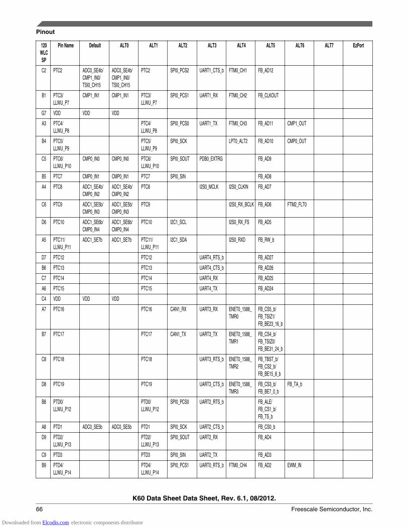
120WLCSP
Pin Name Default ALT0 ALT1 ALT2 ALT3 ALT4 ALT5 ALT6 ALT7 EzPort
C2 PTC2 ADC0_SE4b/CMP1_IN0/TSI0_CH15
ADC0_SE4b/CMP1_IN0/TSI0_CH15
PTC2 SPI0_PCS2 UART1_CTS_b FTM0_CH1 FB_AD12
B1 PTC3/LLWU_P7
CMP1_IN1 CMP1_IN1 PTC3/LLWU_P7
SPI0_PCS1 UART1_RX FTM0_CH2 FB_CLKOUT
G7 VDD VDD VDD
A3 PTC4/LLWU_P8
PTC4/LLWU_P8
SPI0_PCS0 UART1_TX FTM0_CH3 FB_AD11 CMP1_OUT
B4 PTC5/LLWU_P9
PTC5/LLWU_P9
SPI0_SCK LPT0_ALT2 FB_AD10 CMP0_OUT
C5 PTC6/LLWU_P10
CMP0_IN0 CMP0_IN0 PTC6/LLWU_P10
SPI0_SOUT PDB0_EXTRG FB_AD9
B5 PTC7 CMP0_IN1 CMP0_IN1 PTC7 SPI0_SIN FB_AD8
A4 PTC8 ADC1_SE4b/CMP0_IN2
ADC1_SE4b/CMP0_IN2
PTC8 I2S0_MCLK I2S0_CLKIN FB_AD7
C6 PTC9 ADC1_SE5b/CMP0_IN3
ADC1_SE5b/CMP0_IN3
PTC9 I2S0_RX_BCLK FB_AD6 FTM2_FLT0
D6 PTC10 ADC1_SE6b/CMP0_IN4
ADC1_SE6b/CMP0_IN4
PTC10 I2C1_SCL I2S0_RX_FS FB_AD5
A5 PTC11/LLWU_P11
ADC1_SE7b ADC1_SE7b PTC11/LLWU_P11
I2C1_SDA I2S0_RXD FB_RW_b
D7 PTC12 PTC12 UART4_RTS_b FB_AD27
B6 PTC13 PTC13 UART4_CTS_b FB_AD26
C7 PTC14 PTC14 UART4_RX FB_AD25
A6 PTC15 PTC15 UART4_TX FB_AD24
C4 VDD VDD VDD
A7 PTC16 PTC16 CAN1_RX UART3_RX ENET0_1588_TMR0
FB_CS5_b/FB_TSIZ1/FB_BE23_16_b
B7 PTC17 PTC17 CAN1_TX UART3_TX ENET0_1588_TMR1
FB_CS4_b/FB_TSIZ0/FB_BE31_24_b
C8 PTC18 PTC18 UART3_RTS_b ENET0_1588_TMR2
FB_TBST_b/FB_CS2_b/FB_BE15_8_b
D8 PTC19 PTC19 UART3_CTS_b ENET0_1588_TMR3
FB_CS3_b/FB_BE7_0_b
FB_TA_b
B8 PTD0/LLWU_P12
PTD0/LLWU_P12
SPI0_PCS0 UART2_RTS_b FB_ALE/FB_CS1_b/FB_TS_b
A8 PTD1 ADC0_SE5b ADC0_SE5b PTD1 SPI0_SCK UART2_CTS_b FB_CS0_b
D9 PTD2/LLWU_P13
PTD2/LLWU_P13
SPI0_SOUT UART2_RX FB_AD4
C9 PTD3 PTD3 SPI0_SIN UART2_TX FB_AD3
B9 PTD4/LLWU_P14
PTD4/LLWU_P14
SPI0_PCS1 UART0_RTS_b FTM0_CH4 FB_AD2 EWM_IN
Pinout
K60 Data Sheet Data Sheet, Rev. 6.1, 08/2012.
66 Freescale Semiconductor, Inc.
Downloaded from Elcodis.com electronic components distributor
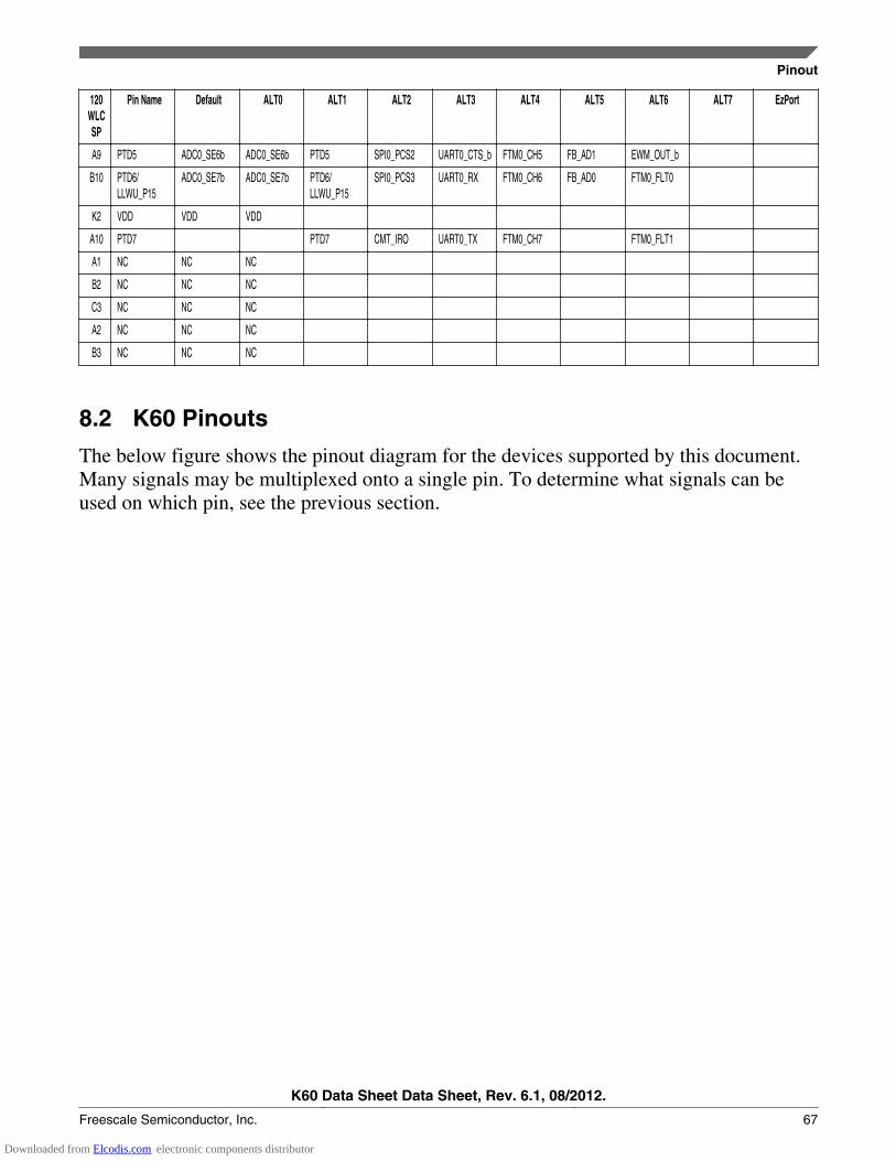
120WLCSP
Pin Name Default ALT0 ALT1 ALT2 ALT3 ALT4 ALT5 ALT6 ALT7 EzPort
A9 PTD5 ADC0_SE6b ADC0_SE6b PTD5 SPI0_PCS2 UART0_CTS_b FTM0_CH5 FB_AD1 EWM_OUT_b
B10 PTD6/LLWU_P15
ADC0_SE7b ADC0_SE7b PTD6/LLWU_P15
SPI0_PCS3 UART0_RX FTM0_CH6 FB_AD0 FTM0_FLT0
K2 VDD VDD VDD
A10 PTD7 PTD7 CMT_IRO UART0_TX FTM0_CH7 FTM0_FLT1
A1 NC NC NC
B2 NC NC NC
C3 NC NC NC
A2 NC NC NC
B3 NC NC NC
8.2 K60 Pinouts
The below figure shows the pinout diagram for the devices supported by this document.Many signals may be multiplexed onto a single pin. To determine what signals can beused on which pin, see the previous section.
Pinout
K60 Data Sheet Data Sheet, Rev. 6.1, 08/2012.
Freescale Semiconductor, Inc. 67
Downloaded from Elcodis.com electronic components distributor
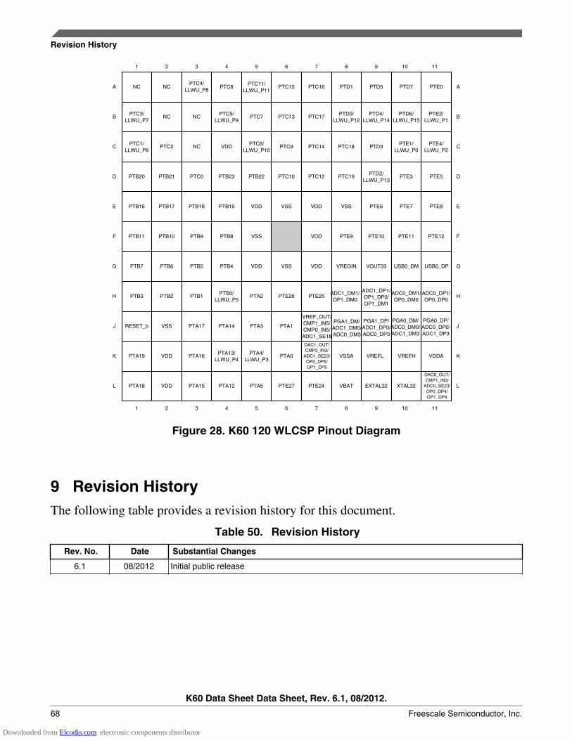
1
A NC
B PTC3/LLWU_P7
C PTC1/LLWU_P6
D PTB20
E PTB16
F PTB11
G PTB7
H PTB3
J RESET_b
K PTA19
1
L PTA18
2
NC
NC
PTC2
PTB21
PTB17
PTB10
PTB6
PTB2
VSS
VDD
2
VDD
3
PTC4/LLWU_P8
NC
NC
PTC0
PTB18
PTB9
PTB5
PTB1
PTA17
PTA16
3
PTA15
4
PTC8
PTC5/LLWU_P9
VDD
PTB23
PTB19
PTB8
PTB4
PTB0/LLWU_P5
PTA14
PTA13/LLWU_P4
4
PTA12
5
PTC11/LLWU_P11
PTC7
PTC6/LLWU_P10
PTB22
VDD
VSS
VDD
PTA2
PTA3
PTA4/LLWU_P3
5
PTA5
6
PTC15
PTC13
PTC9
PTC10
VSS
VSS
PTE26
PTA1
PTA0
6
PTE27
7
PTC16
PTC17
PTC14
PTC12
VDD
VDD
VDD
PTE25
VREF_OUT/CMP1_IN5/CMP0_IN5/ADC1_SE18
DAC1_OUT/CMP2_IN3/
ADC1_SE23/OP0_DP5/OP1_DP5
7
PTE24
8
PTD1
PTD0/LLWU_P12
PTC18
PTC19
VSS
PTE9
VREGIN
ADC1_DM1/OP1_DM0
PGA1_DM/ADC1_DM0/ADC0_DM3
VSSA
8
VBAT
9
PTD5
PTD4/LLWU_P14
PTD3
PTD2/LLWU_P13
PTE6
PTE10
VOUT33
ADC1_DP1/OP1_DP0/OP1_DM1
PGA1_DP/ADC1_DP0/ADC0_DP3
VREFL
9
EXTAL32
10
PTD7
PTD6/LLWU_P15
PTE1/LLWU_P0
PTE3
PTE7
PTE11
USB0_DM
ADC0_DM1/OP0_DM0
PGA0_DM/ADC0_DM0/ADC1_DM3
VREFH
10
XTAL32
11
APTE0
BPTE2/LLWU_P1
CPTE4/LLWU_P2
DPTE5
EPTE8
FPTE12
GUSB0_DP
HADC0_DP1/OP0_DP0
JPGA0_DP/
ADC0_DP0/ADC1_DP3
KVDDA
11
L
DAC0_OUT/CMP1_IN3/
ADC0_SE23/OP0_DP4/OP1_DP4
Figure 28. K60 120 WLCSP Pinout Diagram
9 Revision HistoryThe following table provides a revision history for this document.
Table 50. Revision History
Rev. No. Date Substantial Changes
6.1 08/2012 Initial public release
Revision History
K60 Data Sheet Data Sheet, Rev. 6.1, 08/2012.
68 Freescale Semiconductor, Inc.
Downloaded from Elcodis.com electronic components distributor
How to Reach Us:
Home Page:www.freescale.com
Web Support:http://www.freescale.com/support
USA/Europe or Locations Not Listed:Freescale SemiconductorTechnical Information Center, EL5162100 East Elliot RoadTempe, Arizona 85284+1-800-521-6274 or +1-480-768-2130www.freescale.com/support
Europe, Middle East, and Africa:Freescale Halbleiter Deutschland GmbHTechnical Information CenterSchatzbogen 781829 Muenchen, Germany+44 1296 380 456 (English)+46 8 52200080 (English)+49 89 92103 559 (German)+33 1 69 35 48 48 (French)www.freescale.com/support
Japan:Freescale Semiconductor Japan Ltd.HeadquartersARCO Tower 15F1-8-1, Shimo-Meguro, Meguro-ku,Tokyo 153-0064Japan0120 191014 or +81 3 5437 [email protected]
Asia/Pacific:Freescale Semiconductor China Ltd.Exchange Building 23FNo. 118 Jianguo RoadChaoyang DistrictBeijing 100022China+86 10 5879 [email protected]
Document Number: K60P120M100SF2Rev. 6.1, 08/2012
Information in this document is provided solely to enable system and softwareimplementers to use Freescale Semiconductors products. There are no express or impliedcopyright licenses granted hereunder to design or fabricate any integrated circuits orintegrated circuits based on the information in this document.
Freescale Semiconductor reserves the right to make changes without further notice to anyproducts herein. Freescale Semiconductor makes no warranty, representation, orguarantee regarding the suitability of its products for any particular purpose, nor doesFreescale Semiconductor assume any liability arising out of the application or use of anyproduct or circuit, and specifically disclaims any liability, including without limitationconsequential or incidental damages. "Typical" parameters that may be provided inFreescale Semiconductor data sheets and/or specifications can and do vary in differentapplications and actual performance may vary over time. All operating parameters,including "Typicals", must be validated for each customer application by customer'stechnical experts. Freescale Semiconductor does not convey any license under its patentrights nor the rights of others. Freescale Semiconductor products are not designed,intended, or authorized for use as components in systems intended for surgical implantinto the body, or other applications intended to support or sustain life, or for any otherapplication in which failure of the Freescale Semiconductor product could create asituation where personal injury or death may occur. Should Buyer purchase or useFreescale Semiconductor products for any such unintended or unauthorized application,Buyer shall indemnify Freescale Semiconductor and its officers, employees, subsidiaries,affiliates, and distributors harmless against all claims, costs, damages, and expenses, andreasonable attorney fees arising out of, directly or indirectly, any claim of personal injuryor death associated with such unintended or unauthorized use, even if such claims allegesthat Freescale Semiconductor was negligent regarding the design or manufacture ofthe part.
RoHS-compliant and/or Pb-free versions of Freescale products have the functionality andelectrical characteristics as their non-RoHS-complaint and/or non-Pb-free counterparts.For further information, see http://www.freescale.com or contact your Freescalesales representative.
For information on Freescale's Environmental Products program, go tohttp://www.freescale.com/epp.
Freescale™ and the Freescale logo are trademarks of Freescale Semiconductor, Inc.All other product or service names are the property of their respective owners.
© 2011–2012 Freescale Semiconductor, Inc.
Downloaded from Elcodis.com electronic components distributor