journal of microelectromechanical …xa.yimg.com/kq/groups/13354653/798810434/name/1516191.pdftotal...
TRANSCRIPT
JOURNAL OF MICROELECTROMECHANICAL SYSTEMS, VOL. 14, NO. 5, OCTOBER 2005 1089
Laterally Moving Bistable MEMS DC Switch forBiomedical Applications
Rogier A. M. Receveur, Cornel R. Marxer, Roel Woering, Vincent C. M. H. Larik, andNicolaas-F. de Rooij, Fellow, IEEE
Abstract—In this paper, we have designed a bistable microelec-tromechanical switch for an implantable lead electrode multiplexerapplication. Fabrication is based on a single mask process. Statechanges require an 18 V pulse to the actuators consuming only0.2 nJ energy. The switch does not consume any energy in eitherthe ON or the OFF state. Total chip size including bond pads is ap-proximately 1.5 mm 1.5 mm. The initial contact resistance isbelow 5 with a contact force in the order of 10 N. The contactresistance stays consistently below 30 for the first 40 000 cycles.Breakdown voltage between the two contact members in OFF stateis 300 V. We plan to further investigate applicability of this switchin the biomedical field. [1337]
Index Terms—Deep-reactive ion etching (DRIE), medical,microcontact, switch.
I. INTRODUCTION
I N MANY fields of medicine delivering electrical pulses tothe body via a chronically implanted electrode connected to
an implantable pulse generator (IPG) via a lead can restore a pa-tient’s health. The ability to select electrodes from a plurality ofpossibilities noninvasively enhances the patient’s therapy sincethe stimulation site can be adapted to changes that occur duringhis/her life. In addition the implanting procedure is facilitatedbecause the lead position is less critical, which is advantageousfor both the patient and the physician. A dedicated connectionfrom each electrode to the IPG leads to bulky connector blockson the IPG, thick leads and adaptations of the circuitry in theIPG itself. The lead proposed here has a bipolar Industry Stan-dard (IS-1) connector on the proximal side that plugs in to anyIPG and multiplexer functionality to allow addressing of mul-tiple electrodes on the distal side (Fig. 1). Apart from controllogic, interconnects and possibly power some form of switchingis needed to enable the multiplexing functionality. We will focuson the switches only in this paper.
A single pole single throw (SPST) switch has one signal inputand one signal output terminal. It either transfers the signalfrom the input to the output (ON state) or it does not transfer
Manuscript received May 5, 2004; revised December 6, 2004. This work wassupported in part by a Medtronic Quest Grant. Portions of this paper have ap-peared in a conference publication [1]. Subject Editor E. Obermeier.
R. A. M. Receveur and V. C. M. H. Larik are with the Medtronic BakkenResearch Center, 6229 GW Maastricht, The Netherlands. (e-mail: [email protected]; [email protected]).
C. R. Marxer and N.-F. de Rooij are with the Institute of Micro-technology, University of Neuchâtel, Neuchâtel, 2007 Switzerland (e-mail:[email protected]; [email protected]).
R. Woering was with the Medtronic Bakken Research Center, Maastricht,6229 GW, The Netherlands. He is currently at the Technical University Eind-hoven, Eindhoven, The Netherlands and with www.heliman.com.
Digital Object Identifier 10.1109/JMEMS.2005.851843
it (OFF state). The switch state is controlled via a control ter-minal. Bistable switches do not consume any energy in eitherthe ON or the OFF state. Monostable switches are either OFF orON in the absence of a control signal (normally open or normallyclosed respectively). They constantly consume energy to stay inthe “abnormal” state (ON or OFF, respectively). The main advan-tages of monostable microelectromechanical system (MEMS)switches over conventional solid state switches are low power[2], [3], low-contact resistance, small size, and high breakdownvoltage [3]. The additional advantage of bistable over monos-table switches is the zero energy consumption in both states,providing even lower power and state retention in case of powerfailure (Table I).
The signal from the IPG contains 4 ms pulses. We specifya MEMS switch that is able to transfer dc current, in contrastto RF-MEMS switches. There are numerous mono stable microelectro mechanical dc-switches [4]–[11]. Bistable switches without of plane movement of contact members use either a currentpulse to change the preferential magnetization of a permalloycantilever in a permanent external magnetic field [12] or a me-chanical latch caused by a thermally actuated two segment mul-timorph cantilever [13]. Laterally moving bistable switches usea compliant structure consisting out of a central slider supportedby double pinned arms on both sides [3] or two double pinnedarms pushed in two possible directions by actuators on bothsides [2]. An overview of the reported properties of these de-vices is given in Table III and Table IV.
We present a novel design for a laterally moving bistabledc-switch. The bistable part of the design was proposed byHichwa et al. to build an optical switch [14]. It has a centralmoving contact member with two stable positions. This isachieved by a dual spring suspension system with hinges anddouble clamped beams as qualitatively explained in Fig. 2 andFig. 3. In our design an opposing contact member is contactedin the second stable position that closes the electrical contact.Electrostatic comb actuators can change the switch position.The contact is designed to meet the target specifications givenin Table I.
In this contribution we focus on the design and characteri-zation of the electrical switch and its long-term contact prop-erties. In Section II the fabrication process, switch layout in-cluding definitions of switch parameters and experimental setupare given. Theoretical expressions describing switch propertiesin terms of the parameters are provided in Section III. Designchoices are made in Section IV-A resulting in actual parametervalues given in Table II. The remainder of Section IV presentsmeasurement results and a comparison with theory by applying
1057-7157/$20.00 © 2005 IEEE
Authorized licensed use limited to: UNIVERSITE LOUIS PASTEUR. Downloaded on May 26,2010 at 09:13:35 UTC from IEEE Xplore. Restrictions apply.
1090 JOURNAL OF MICROELECTROMECHANICAL SYSTEMS, VOL. 14, NO. 5, OCTOBER 2005
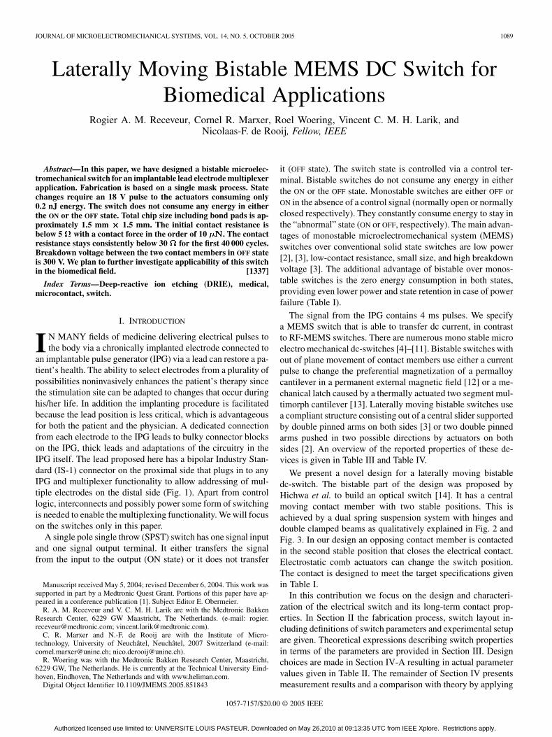
Fig. 1. Implantable Pulse Generator (IPG) with two bipolar Industry Standard (IS-1) connectors. One lead is shown having a bipolar IS-1 connector on theproximal side and eight electrodes on the distal side (labeled STIMLEAD) connected via an IN-LINE connector. The SMARTLEAD contains switches andcommunication-and control logic that allow selection of any (combination of) electrode(s) on the stimlead to deliver optimal therapy.
TABLE ITARGET SPECIFICATIONS FOR BI-STABLE MEMS SWITCH. FET SWITCH
SPECIFICATIONS ARE GIVEN TO SHOW ADVANTAGES OF MEMS SWITCH
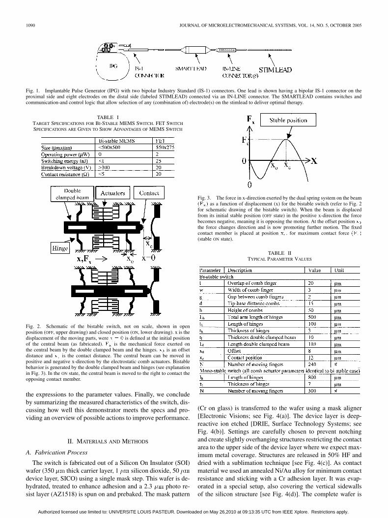
Fig. 2. Schematic of the bistable switch, not on scale, shown in openposition (OFF, upper drawing) and closed position (ON, lower drawing). x is thedisplacement of the moving parts, were x = 0 is defined at the initial positionof the central beam (as fabricated). F is the mechanical force exerted onthe central beam by the double clamped beam and the hinges. x is an offsetdistance and x is the contact distance. The central beam can be moved inpositive and negative x-direction by the electrostatic comb actuators. Bistablebehavior is generated by the double clamped beam and hinges (see explanationin Fig. 3). In the ON state, the central beam is moved to the right to contact theopposing contact member.
the expressions to the parameter values. Finally, we concludeby summarizing the measured characteristics of the switch, dis-cussing how well this demonstrator meets the specs and pro-viding an overview of possible actions to improve performance.
II. MATERIALS AND METHODS
A. Fabrication Process
The switch is fabricated out of a Silicon On Insulator (SOI)wafer (350 thick carrier layer, 1 silicon dioxide, 50device layer, SICO) using a single mask step. This wafer is de-hydrated, treated to enhance adhesion and a 2.3 photo re-sist layer (AZ1518) is spun on and prebaked. The mask pattern
Fig. 3. The force in x-direction exerted by the dual spring system on the beam(F ) as a function of displacement (x) for the bistable switch (refer to Fig. 2for schematic drawing of the bistable switch). When the beam is displacedfrom its initial stable position (OFF state) in the positive x-direction the forcebecomes negative, meaning it is opposing the motion. At the offset position xthe force changes direction and is now promoting further motion. The fixedcontact member is placed at position x . for maximum contact force (F )(stable ON state).
TABLE IITYPICAL PARAMETER VALUES
(Cr on glass) is transferred to the wafer using a mask aligner[Electronic Visions; see Fig. 4(a)]. The device layer is deep-reactive ion etched [DRIE, Surface Technology Systems; seeFig. 4(b)]. Settings are carefully chosen to prevent notchingand create slightly overhanging structures restricting the contactarea to the upper side of the device layer where we expect max-imum metal coverage. Structures are released in 50% HF anddried with a sublimation technique [see Fig. 4(c)]. As contactmaterial we used an annealed Ni/Au alloy for minimum contactresistance and sticking with a Cr adhesion layer. It was evap-orated in a special setup, also covering the vertical sidewallsof the silicon structure [see Fig. 4(d)]. The complete wafer is
Authorized licensed use limited to: UNIVERSITE LOUIS PASTEUR. Downloaded on May 26,2010 at 09:13:35 UTC from IEEE Xplore. Restrictions apply.
RECEVEUR et al.: LATERALLY MOVING BISTABLE MEMS DC SWITCH FOR BIOMEDICAL APPLICATIONS 1091
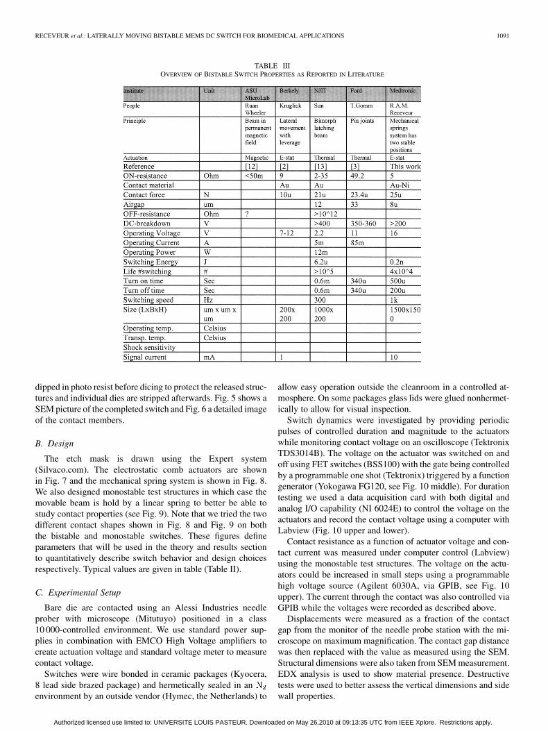
TABLE IIIOVERVIEW OF BISTABLE SWITCH PROPERTIES AS REPORTED IN LITERATURE
dipped in photo resist before dicing to protect the released struc-tures and individual dies are stripped afterwards. Fig. 5 shows aSEM picture of the completed switch and Fig. 6 a detailed imageof the contact members.
B. Design
The etch mask is drawn using the Expert system(Silvaco.com). The electrostatic comb actuators are shownin Fig. 7 and the mechanical spring system is shown in Fig. 8.We also designed monostable test structures in which case themovable beam is hold by a linear spring to better be able tostudy contact properties (see Fig. 9). Note that we tried the twodifferent contact shapes shown in Fig. 8 and Fig. 9 on boththe bistable and monostable switches. These figures defineparameters that will be used in the theory and results sectionto quantitatively describe switch behavior and design choicesrespectively. Typical values are given in table (Table II).
C. Experimental Setup
Bare die are contacted using an Alessi Industries needleprober with microscope (Mitutuyo) positioned in a class10 000-controlled environment. We use standard power sup-plies in combination with EMCO High Voltage amplifiers tocreate actuation voltage and standard voltage meter to measurecontact voltage.
Switches were wire bonded in ceramic packages (Kyocera,8 lead side brazed package) and hermetically sealed in anenvironment by an outside vendor (Hymec, the Netherlands) to
allow easy operation outside the cleanroom in a controlled at-mosphere. On some packages glass lids were glued nonhermet-ically to allow for visual inspection.
Switch dynamics were investigated by providing periodicpulses of controlled duration and magnitude to the actuatorswhile monitoring contact voltage on an oscilloscope (TektronixTDS3014B). The voltage on the actuator was switched on andoff using FET switches (BSS100) with the gate being controlledby a programmable one shot (Tektronix) triggered by a functiongenerator (Yokogawa FG120, see Fig. 10 middle). For durationtesting we used a data acquisition card with both digital andanalog I/O capability (NI 6024E) to control the voltage on theactuators and record the contact voltage using a computer withLabview (Fig. 10 upper and lower).
Contact resistance as a function of actuator voltage and con-tact current was measured under computer control (Labview)using the monostable test structures. The voltage on the actu-ators could be increased in small steps using a programmablehigh voltage source (Agilent 6030A, via GPIB, see Fig. 10upper). The current through the contact was also controlled viaGPIB while the voltages were recorded as described above.
Displacements were measured as a fraction of the contactgap from the monitor of the needle probe station with the mi-croscope on maximum magnification. The contact gap distancewas then replaced with the value as measured using the SEM.Structural dimensions were also taken from SEM measurement.EDX analysis is used to show material presence. Destructivetests were used to better assess the vertical dimensions and sidewall properties.
Authorized licensed use limited to: UNIVERSITE LOUIS PASTEUR. Downloaded on May 26,2010 at 09:13:35 UTC from IEEE Xplore. Restrictions apply.
1092 JOURNAL OF MICROELECTROMECHANICAL SYSTEMS, VOL. 14, NO. 5, OCTOBER 2005
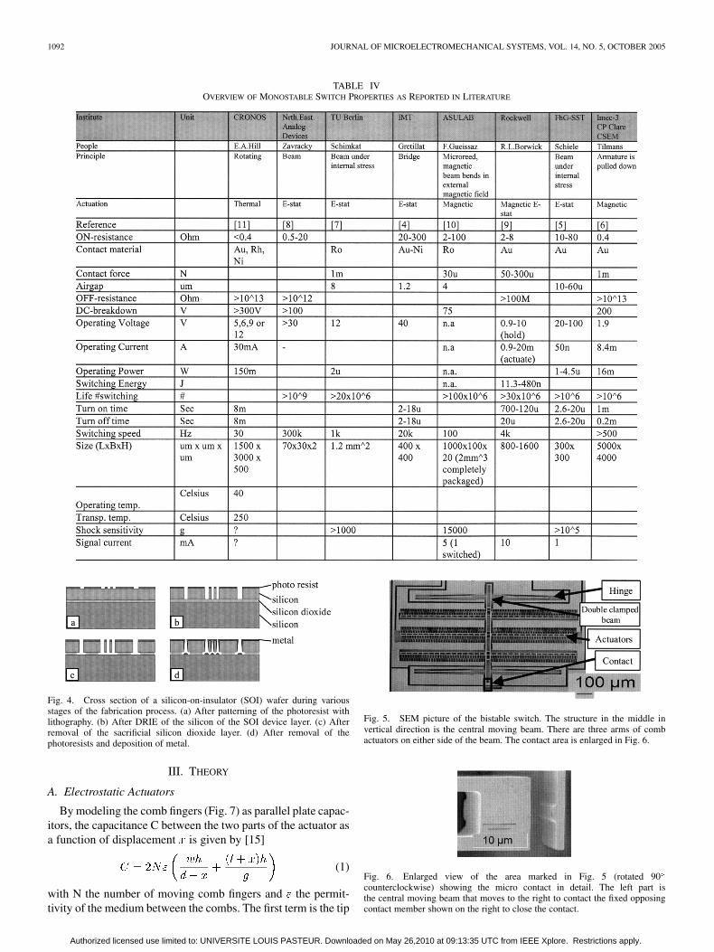
TABLE IVOVERVIEW OF MONOSTABLE SWITCH PROPERTIES AS REPORTED IN LITERATURE
Fig. 4. Cross section of a silicon-on-insulator (SOI) wafer during variousstages of the fabrication process. (a) After patterning of the photoresist withlithography. (b) After DRIE of the silicon of the SOI device layer. (c) Afterremoval of the sacrificial silicon dioxide layer. (d) After removal of thephotoresists and deposition of metal.
III. THEORY
A. Electrostatic Actuators
By modeling the comb fingers (Fig. 7) as parallel plate capac-itors, the capacitance C between the two parts of the actuator asa function of displacement is given by [15]
(1)
with N the number of moving comb fingers and the permit-tivity of the medium between the combs. The first term is the tip
Fig. 5. SEM picture of the bistable switch. The structure in the middle invertical direction is the central moving beam. There are three arms of combactuators on either side of the beam. The contact area is enlarged in Fig. 6.
Fig. 6. Enlarged view of the area marked in Fig. 5 (rotated 90counterclockwise) showing the micro contact in detail. The left part isthe central moving beam that moves to the right to contact the fixed opposingcontact member shown on the right to close the contact.
Authorized licensed use limited to: UNIVERSITE LOUIS PASTEUR. Downloaded on May 26,2010 at 09:13:35 UTC from IEEE Xplore. Restrictions apply.
RECEVEUR et al.: LATERALLY MOVING BISTABLE MEMS DC SWITCH FOR BIOMEDICAL APPLICATIONS 1093
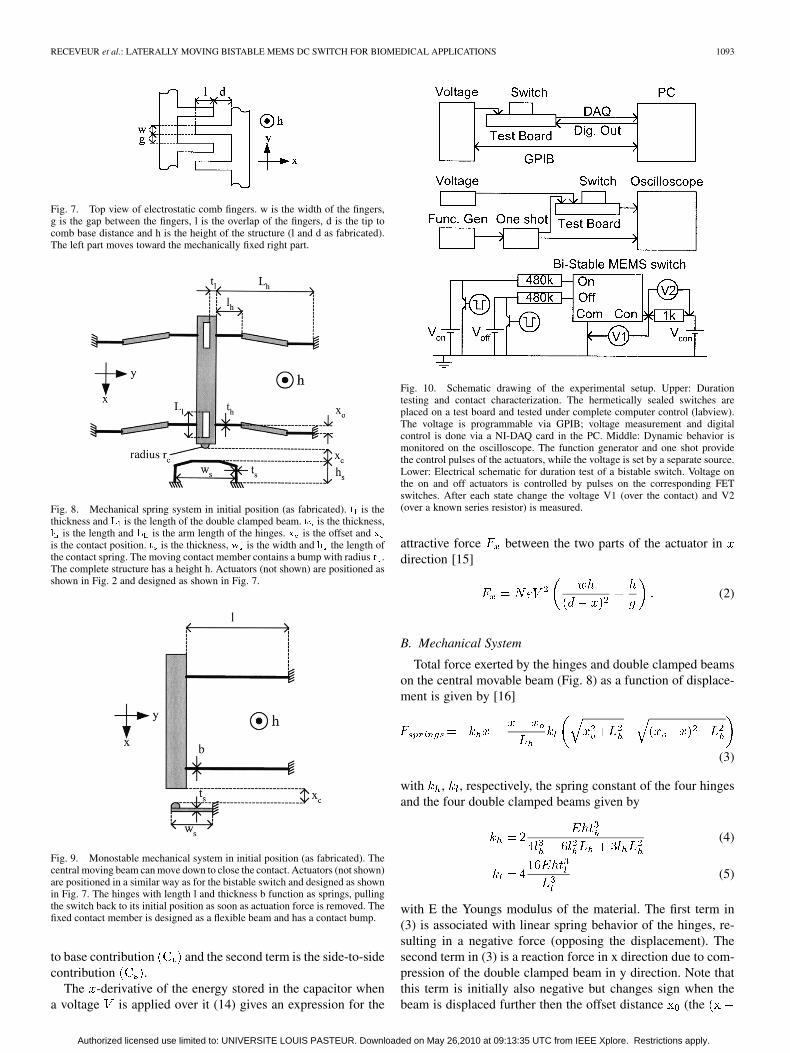
Fig. 7. Top view of electrostatic comb fingers. w is the width of the fingers,g is the gap between the fingers, l is the overlap of the fingers, d is the tip tocomb base distance and h is the height of the structure (l and d as fabricated).The left part moves toward the mechanically fixed right part.
Fig. 8. Mechanical spring system in initial position (as fabricated). t is thethickness and L is the length of the double clamped beam. t is the thickness,l is the length and L is the arm length of the hinges. x is the offset and x
is the contact position. t is the thickness, w is the width and h the length ofthe contact spring. The moving contact member contains a bump with radius r .The complete structure has a height h. Actuators (not shown) are positioned asshown in Fig. 2 and designed as shown in Fig. 7.
Fig. 9. Monostable mechanical system in initial position (as fabricated). Thecentral moving beam can move down to close the contact. Actuators (not shown)are positioned in a similar way as for the bistable switch and designed as shownin Fig. 7. The hinges with length l and thickness b function as springs, pullingthe switch back to its initial position as soon as actuation force is removed. Thefixed contact member is designed as a flexible beam and has a contact bump.
to base contribution and the second term is the side-to-sidecontribution .
The -derivative of the energy stored in the capacitor whena voltage is applied over it (14) gives an expression for the
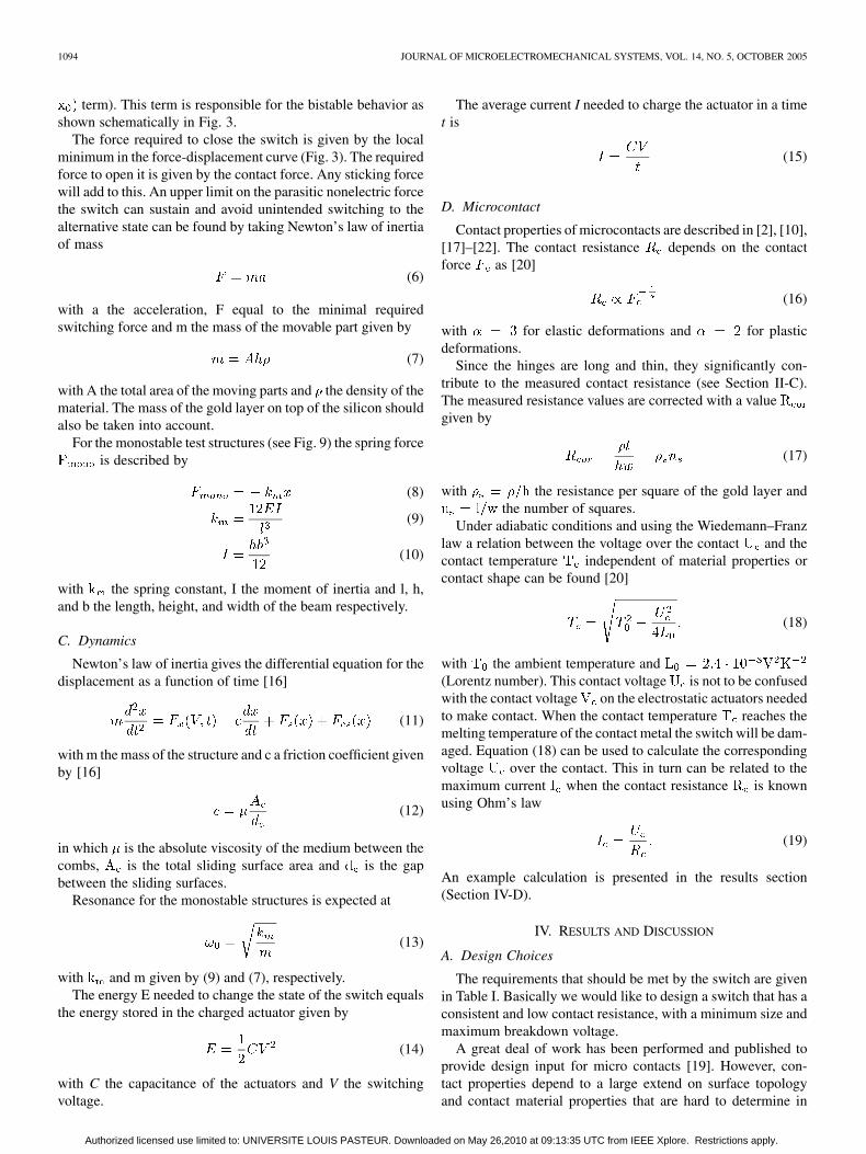
Fig. 10. Schematic drawing of the experimental setup. Upper: Durationtesting and contact characterization. The hermetically sealed switches areplaced on a test board and tested under complete computer control (labview).The voltage is programmable via GPIB; voltage measurement and digitalcontrol is done via a NI-DAQ card in the PC. Middle: Dynamic behavior ismonitored on the oscilloscope. The function generator and one shot providethe control pulses of the actuators, while the voltage is set by a separate source.Lower: Electrical schematic for duration test of a bistable switch. Voltage onthe on and off actuators is controlled by pulses on the corresponding FETswitches. After each state change the voltage V1 (over the contact) and V2(over a known series resistor) is measured.
attractive force between the two parts of the actuator indirection [15]
(2)
B. Mechanical System
Total force exerted by the hinges and double clamped beamson the central movable beam (Fig. 8) as a function of displace-ment is given by [16]
(3)
with , , respectively, the spring constant of the four hingesand the four double clamped beams given by
(4)
(5)
with E the Youngs modulus of the material. The first term in(3) is associated with linear spring behavior of the hinges, re-sulting in a negative force (opposing the displacement). Thesecond term in (3) is a reaction force in x direction due to com-pression of the double clamped beam in y direction. Note thatthis term is initially also negative but changes sign when thebeam is displaced further then the offset distance (the
Authorized licensed use limited to: UNIVERSITE LOUIS PASTEUR. Downloaded on May 26,2010 at 09:13:35 UTC from IEEE Xplore. Restrictions apply.
1094 JOURNAL OF MICROELECTROMECHANICAL SYSTEMS, VOL. 14, NO. 5, OCTOBER 2005
term). This term is responsible for the bistable behavior asshown schematically in Fig. 3.
The force required to close the switch is given by the localminimum in the force-displacement curve (Fig. 3). The requiredforce to open it is given by the contact force. Any sticking forcewill add to this. An upper limit on the parasitic nonelectric forcethe switch can sustain and avoid unintended switching to thealternative state can be found by taking Newton’s law of inertiaof mass
(6)
with a the acceleration, F equal to the minimal requiredswitching force and m the mass of the movable part given by
(7)
with A the total area of the moving parts and the density of thematerial. The mass of the gold layer on top of the silicon shouldalso be taken into account.
For the monostable test structures (see Fig. 9) the spring forceis described by
(8)
(9)
(10)
with the spring constant, I the moment of inertia and l, h,and b the length, height, and width of the beam respectively.
C. Dynamics
Newton’s law of inertia gives the differential equation for thedisplacement as a function of time [16]
(11)
with m the mass of the structure and c a friction coefficient givenby [16]
(12)
in which is the absolute viscosity of the medium between thecombs, is the total sliding surface area and is the gapbetween the sliding surfaces.
Resonance for the monostable structures is expected at
(13)
with and m given by (9) and (7), respectively.The energy E needed to change the state of the switch equals
the energy stored in the charged actuator given by
(14)
with C the capacitance of the actuators and V the switchingvoltage.
The average current I needed to charge the actuator in a timet is
(15)
D. Microcontact
Contact properties of microcontacts are described in [2], [10],[17]–[22]. The contact resistance depends on the contactforce as [20]
(16)
with for elastic deformations and for plasticdeformations.
Since the hinges are long and thin, they significantly con-tribute to the measured contact resistance (see Section II-C).The measured resistance values are corrected with a valuegiven by
(17)
with the resistance per square of the gold layer andthe number of squares.
Under adiabatic conditions and using the Wiedemann–Franzlaw a relation between the voltage over the contact and thecontact temperature independent of material properties orcontact shape can be found [20]
(18)
with the ambient temperature and(Lorentz number). This contact voltage is not to be confusedwith the contact voltage on the electrostatic actuators neededto make contact. When the contact temperature reaches themelting temperature of the contact metal the switch will be dam-aged. Equation (18) can be used to calculate the correspondingvoltage over the contact. This in turn can be related to themaximum current when the contact resistance is knownusing Ohm’s law
(19)
An example calculation is presented in the results section(Section IV-D).
IV. RESULTS AND DISCUSSION
A. Design Choices
The requirements that should be met by the switch are givenin Table I. Basically we would like to design a switch that has aconsistent and low contact resistance, with a minimum size andmaximum breakdown voltage.
A great deal of work has been performed and published toprovide design input for micro contacts [19]. However, con-tact properties depend to a large extend on surface topologyand contact material properties that are hard to determine in
Authorized licensed use limited to: UNIVERSITE LOUIS PASTEUR. Downloaded on May 26,2010 at 09:13:35 UTC from IEEE Xplore. Restrictions apply.
RECEVEUR et al.: LATERALLY MOVING BISTABLE MEMS DC SWITCH FOR BIOMEDICAL APPLICATIONS 1095
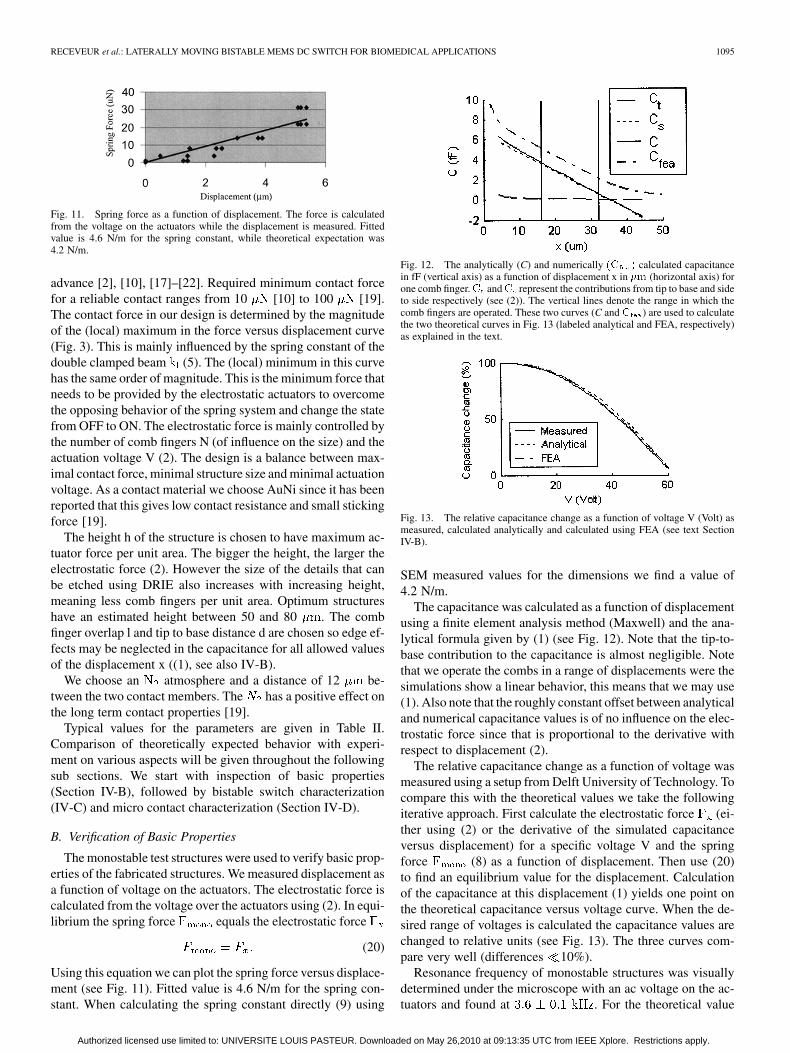
Fig. 11. Spring force as a function of displacement. The force is calculatedfrom the voltage on the actuators while the displacement is measured. Fittedvalue is 4.6 N/m for the spring constant, while theoretical expectation was4.2 N/m.
advance [2], [10], [17]–[22]. Required minimum contact forcefor a reliable contact ranges from 10 [10] to 100 [19].The contact force in our design is determined by the magnitudeof the (local) maximum in the force versus displacement curve(Fig. 3). This is mainly influenced by the spring constant of thedouble clamped beam (5). The (local) minimum in this curvehas the same order of magnitude. This is the minimum force thatneeds to be provided by the electrostatic actuators to overcomethe opposing behavior of the spring system and change the statefrom OFF to ON. The electrostatic force is mainly controlled bythe number of comb fingers N (of influence on the size) and theactuation voltage V (2). The design is a balance between max-imal contact force, minimal structure size and minimal actuationvoltage. As a contact material we choose AuNi since it has beenreported that this gives low contact resistance and small stickingforce [19].
The height h of the structure is chosen to have maximum ac-tuator force per unit area. The bigger the height, the larger theelectrostatic force (2). However the size of the details that canbe etched using DRIE also increases with increasing height,meaning less comb fingers per unit area. Optimum structureshave an estimated height between 50 and 80 . The combfinger overlap l and tip to base distance d are chosen so edge ef-fects may be neglected in the capacitance for all allowed valuesof the displacement x ((1), see also IV-B).
We choose an atmosphere and a distance of 12 be-tween the two contact members. The has a positive effect onthe long term contact properties [19].
Typical values for the parameters are given in Table II.Comparison of theoretically expected behavior with experi-ment on various aspects will be given throughout the followingsub sections. We start with inspection of basic properties(Section IV-B), followed by bistable switch characterization(IV-C) and micro contact characterization (Section IV-D).
B. Verification of Basic Properties
The monostable test structures were used to verify basic prop-erties of the fabricated structures. We measured displacement asa function of voltage on the actuators. The electrostatic force iscalculated from the voltage over the actuators using (2). In equi-librium the spring force equals the electrostatic force
(20)
Using this equation we can plot the spring force versus displace-ment (see Fig. 11). Fitted value is 4.6 N/m for the spring con-stant. When calculating the spring constant directly (9) using
Fig. 12. The analytically (C) and numerically (C ) calculated capacitancein fF (vertical axis) as a function of displacement x in �m (horizontal axis) forone comb finger.C andC represent the contributions from tip to base and sideto side respectively (see (2)). The vertical lines denote the range in which thecomb fingers are operated. These two curves (C and C ) are used to calculatethe two theoretical curves in Fig. 13 (labeled analytical and FEA, respectively)as explained in the text.
Fig. 13. The relative capacitance change as a function of voltage V (Volt) asmeasured, calculated analytically and calculated using FEA (see text SectionIV-B).
SEM measured values for the dimensions we find a value of4.2 N/m.
The capacitance was calculated as a function of displacementusing a finite element analysis method (Maxwell) and the ana-lytical formula given by (1) (see Fig. 12). Note that the tip-to-base contribution to the capacitance is almost negligible. Notethat we operate the combs in a range of displacements were thesimulations show a linear behavior, this means that we may use(1). Also note that the roughly constant offset between analyticaland numerical capacitance values is of no influence on the elec-trostatic force since that is proportional to the derivative withrespect to displacement (2).
The relative capacitance change as a function of voltage wasmeasured using a setup from Delft University of Technology. Tocompare this with the theoretical values we take the followingiterative approach. First calculate the electrostatic force (ei-ther using (2) or the derivative of the simulated capacitanceversus displacement) for a specific voltage V and the springforce (8) as a function of displacement. Then use (20)to find an equilibrium value for the displacement. Calculationof the capacitance at this displacement (1) yields one point onthe theoretical capacitance versus voltage curve. When the de-sired range of voltages is calculated the capacitance values arechanged to relative units (see Fig. 13). The three curves com-pare very well (differences 10%).
Resonance frequency of monostable structures was visuallydetermined under the microscope with an ac voltage on the ac-tuators and found at . For the theoretical value
Authorized licensed use limited to: UNIVERSITE LOUIS PASTEUR. Downloaded on May 26,2010 at 09:13:35 UTC from IEEE Xplore. Restrictions apply.
1096 JOURNAL OF MICROELECTROMECHANICAL SYSTEMS, VOL. 14, NO. 5, OCTOBER 2005
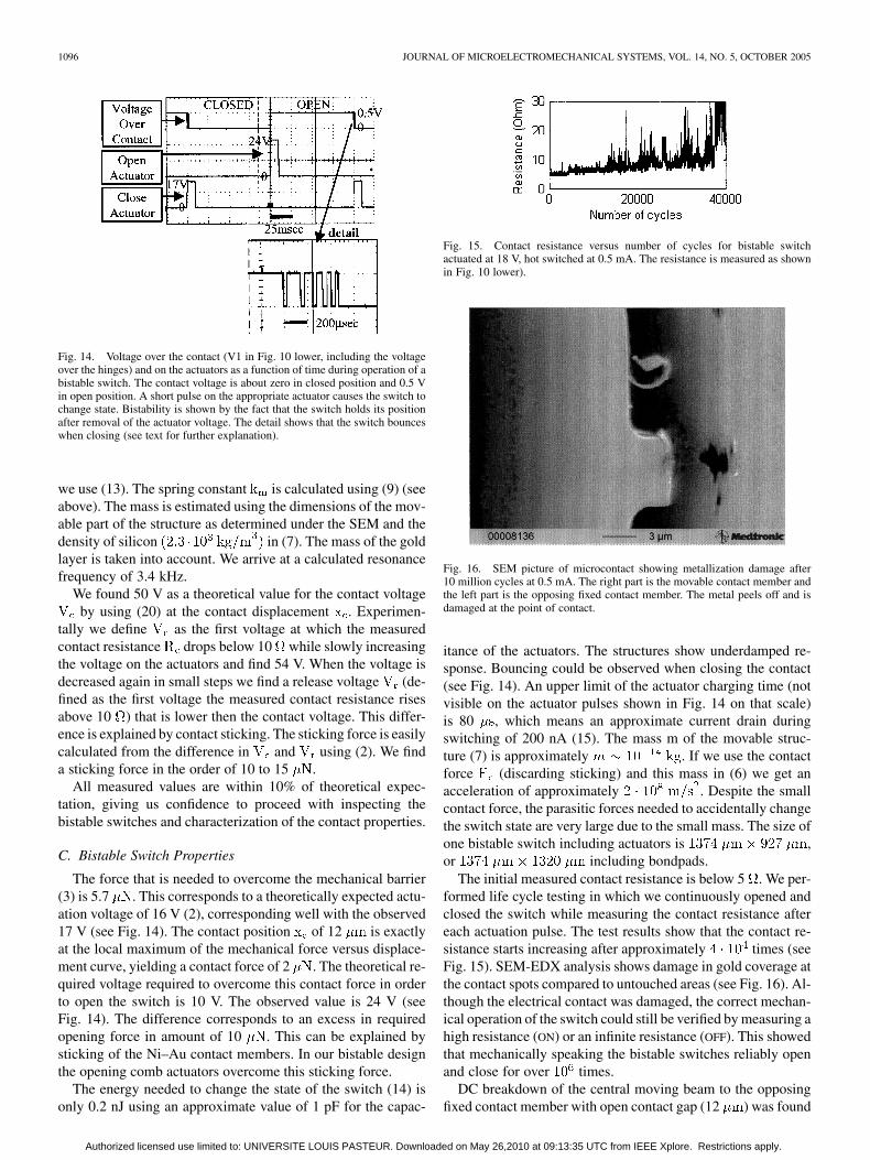
Fig. 14. Voltage over the contact (V1 in Fig. 10 lower, including the voltageover the hinges) and on the actuators as a function of time during operation of abistable switch. The contact voltage is about zero in closed position and 0.5 Vin open position. A short pulse on the appropriate actuator causes the switch tochange state. Bistability is shown by the fact that the switch holds its positionafter removal of the actuator voltage. The detail shows that the switch bounceswhen closing (see text for further explanation).
we use (13). The spring constant is calculated using (9) (seeabove). The mass is estimated using the dimensions of the mov-able part of the structure as determined under the SEM and thedensity of silicon in (7). The mass of the goldlayer is taken into account. We arrive at a calculated resonancefrequency of 3.4 kHz.
We found 50 V as a theoretical value for the contact voltageby using (20) at the contact displacement . Experimen-
tally we define as the first voltage at which the measuredcontact resistance drops below 10 while slowly increasingthe voltage on the actuators and find 54 V. When the voltage isdecreased again in small steps we find a release voltage (de-fined as the first voltage the measured contact resistance risesabove 10 ) that is lower then the contact voltage. This differ-ence is explained by contact sticking. The sticking force is easilycalculated from the difference in and using (2). We finda sticking force in the order of 10 to 15 .
All measured values are within 10% of theoretical expec-tation, giving us confidence to proceed with inspecting thebistable switches and characterization of the contact properties.
C. Bistable Switch Properties
The force that is needed to overcome the mechanical barrier(3) is 5.7 . This corresponds to a theoretically expected actu-ation voltage of 16 V (2), corresponding well with the observed17 V (see Fig. 14). The contact position of 12 is exactlyat the local maximum of the mechanical force versus displace-ment curve, yielding a contact force of 2 . The theoretical re-quired voltage required to overcome this contact force in orderto open the switch is 10 V. The observed value is 24 V (seeFig. 14). The difference corresponds to an excess in requiredopening force in amount of 10 . This can be explained bysticking of the Ni–Au contact members. In our bistable designthe opening comb actuators overcome this sticking force.
The energy needed to change the state of the switch (14) isonly 0.2 nJ using an approximate value of 1 pF for the capac-
Fig. 15. Contact resistance versus number of cycles for bistable switchactuated at 18 V, hot switched at 0.5 mA. The resistance is measured as shownin Fig. 10 lower).
Fig. 16. SEM picture of microcontact showing metallization damage after10 million cycles at 0.5 mA. The right part is the movable contact member andthe left part is the opposing fixed contact member. The metal peels off and isdamaged at the point of contact.
itance of the actuators. The structures show underdamped re-sponse. Bouncing could be observed when closing the contact(see Fig. 14). An upper limit of the actuator charging time (notvisible on the actuator pulses shown in Fig. 14 on that scale)is 80 , which means an approximate current drain duringswitching of 200 nA (15). The mass m of the movable struc-ture (7) is approximately . If we use the contactforce (discarding sticking) and this mass in (6) we get anacceleration of approximately . Despite the smallcontact force, the parasitic forces needed to accidentally changethe switch state are very large due to the small mass. The size ofone bistable switch including actuators is ,or including bondpads.
The initial measured contact resistance is below 5 . We per-formed life cycle testing in which we continuously opened andclosed the switch while measuring the contact resistance aftereach actuation pulse. The test results show that the contact re-sistance starts increasing after approximately times (seeFig. 15). SEM-EDX analysis shows damage in gold coverage atthe contact spots compared to untouched areas (see Fig. 16). Al-though the electrical contact was damaged, the correct mechan-ical operation of the switch could still be verified by measuring ahigh resistance (ON) or an infinite resistance (OFF). This showedthat mechanically speaking the bistable switches reliably openand close for over times.
DC breakdown of the central moving beam to the opposingfixed contact member with open contact gap (12 ) was found
Authorized licensed use limited to: UNIVERSITE LOUIS PASTEUR. Downloaded on May 26,2010 at 09:13:35 UTC from IEEE Xplore. Restrictions apply.
RECEVEUR et al.: LATERALLY MOVING BISTABLE MEMS DC SWITCH FOR BIOMEDICAL APPLICATIONS 1097
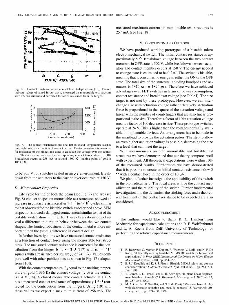
Fig. 17. Contact resistance versus contact force (adapted from [10]). Crossesindicate values obtained in our work, measured on monostable test structurewith 0.5 mA current and corrected for series resistance from the hinges.
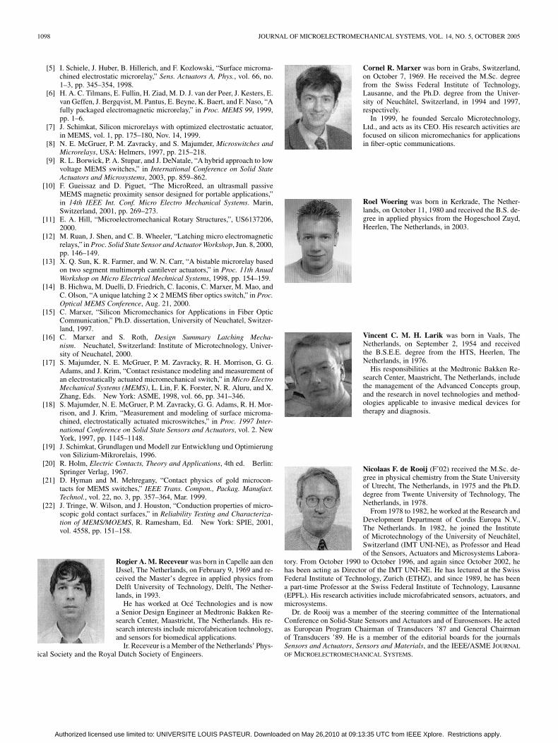
Fig. 18. The contact-resistance (solid line, left axis) and -temperature (dashedline, right axis) as a function of contact current. Contact resistance is correctedfor resistance of the hinges and used to calculate the voltage over the contactU . This is used to calculate the corresponding contact temperature T (18).Breakdown occurs at 258 mA or around 1300 C (melting point of gold is1063 C).
to be 305 V for switches sealed in an environment. Break-down from the actuators to the carrier layer occurred at 150 V.
D. Microcontact Properties
Life cycle testing of both the beam (see Fig. 9) and arc (seeFig. 8) contact shapes on monostable test structures showed anincrease in contact resistance after to cycles similarto that observed for the bistable switch as described above. SEMinspection showed a damaged contact metal similar to that of thebistable switch shown in Fig. 16. These observations do not re-veal a difference in duration behavior between the two contactshapes. The limited robustness of the contact metal is more im-portant then the (small) difference in contact design.
In further investigations we have measured contact resistanceas a function of contact force using the monostable test struc-tures. The measured contact resistance is corrected for the con-tribution from the hinges ((17) withsquares with a resistance per square of 24 ). Values com-pare well with other publications as shown in Fig. 17 (adaptedfrom [10]).
With the contact temperature equal to the melting temper-ature of gold (1336 K) the contact voltage over the contactis 0.4 V (18). A closed monostable contact actuated at 100 Vhas a measured contact resistance of approximately 1.6 (cor-rected for the contribution from the hinges). Using (19) withthese values we expect a maximum current of 258 mA. The
measured maximum current on mono stable test structures is257 mA (see Fig. 18).
V. CONCLUSION AND OUTLOOK
We have produced working prototypes of a bistable microelectro mechanical switch. The initial contact resistance is ap-proximately 5 . Breakdown voltage between the two contactmembers in OFF state is 302 V, while breakdown between actu-ators and contact member occurs at 150 V. The energy neededto change state is estimated to be 0.2 nJ. The switch is bistable,meaning that it consumes no energy in either the ON or the OFFstate. The total size of the structure including bondpads and ac-tuators is . Therefore we have achievedadvantages over FET switches in terms of power consumption,contact resistance and breakdown voltage (see Table I). The sizetarget is not met by these prototypes. However, we can inter-change size with actuation voltage rather effectively. Actuationforce is proportional to the square of the actuation voltage andlinear with the number of comb fingers that are also linear pro-portional to the size. Therefore a factor of 10 in actuation voltagemeans a factor of 100 decrease in size. These prototype switchesoperate at 24 V. This is higher then the voltages normally avail-able in implantable devices. An arrangement has to be made inthe smartlead to provide the actuation pulses. The step to allowan even higher actuation voltage is possible, decreasing the sizeto a level that can meet the target.
With measurements on both monostable and bistable teststructures we have demonstrated that our theory compares wellwith experiment. All theoretical expectations were within 10%of the measured results. Furthermore we have demonstratedthat it is possible to create an initial contact resistance below 5
with a contact force in the order of 10 .We plan to further investigate the applicability of this switch
in the biomedical field. The focal areas will be the contact met-allization and the reliability of the switch. Further fundamentalinvestigation into the dynamics, the sticking force and a theoret-ical treatment of the contact resistance to be expected are alsoconsidered.
ACKNOWLEDGMENT
The authors would like to thank R. C. Hamlen fromMedtronic for capacitance calculations and R. F. Wolffenbutteland L. A. Rocha from Delft University of Technology forperforming the relative capacitance measurements.
REFERENCES
[1] R. Receveur, C. Marxer, F. Duport, R. Woering, V. Larik, and N. F. DeRooij, “A laterally moving bi-stable MEMS DC switch for biomedicalapplications,” in Proc. IEEE International Conference on Micro ElectroMechanical Systems, 2004, pp. 854–856.
[2] E. J. J. Kruglick and K. S. J. Pister, “Bistable MEMS relays and contactcharacterization,” J. Microelectromech. Syst., vol. 8, no. 3, pp. 264–271,Jun. 1999.
[3] T. Gomm, L. L. Howell, and R. H. Selfridge, “In-plane linear displace-ment bistable microrelay,” J. Micromech. Microeng., vol. 2002, no. 12,pp. 257–264, 2002.
[4] M. A. Gretillat, F. Gretillat, and N. F. de Rooij, “Micromechanical relaywith electrostatic actuation and metallic contacts,” J. Micromech. Mi-croeng., no. 9, pp. 324–331, 1999.
Authorized licensed use limited to: UNIVERSITE LOUIS PASTEUR. Downloaded on May 26,2010 at 09:13:35 UTC from IEEE Xplore. Restrictions apply.
1098 JOURNAL OF MICROELECTROMECHANICAL SYSTEMS, VOL. 14, NO. 5, OCTOBER 2005
[5] I. Schiele, J. Huber, B. Hillerich, and F. Kozlowski, “Surface microma-chined electrostatic microrelay,” Sens. Actuators A, Phys., vol. 66, no.1–3, pp. 345–354, 1998.
[6] H. A. C. Tilmans, E. Fullin, H. Ziad, M. D. J. van der Peer, J. Kesters, E.van Geffen, J. Bergqvist, M. Pantus, E. Beyne, K. Baert, and F. Naso, “Afully packaged electromagnetic microrelay,” in Proc. MEMS 99, 1999,pp. 1–6.
[7] J. Schimkat, Silicon microrelays with optimized electrostatic actuator,in MEMS, vol. 1, pp. 175–180, Nov. 14, 1999.
[8] N. E. McGruer, P. M. Zavracky, and S. Majumder, Microswitches andMicrorelays, USA: Helmers, 1997, pp. 215–218.
[9] R. L. Borwick, P. A. Stupar, and J. DeNatale, “A hybrid approach to lowvoltage MEMS switches,” in International Conference on Solid StateActuators and Microsystems, 2003, pp. 859–862.
[10] F. Gueissaz and D. Piguet, “The MicroReed, an ultrasmall passiveMEMS magnetic proximity sensor designed for portable applications,”in 14th IEEE Int. Conf. Micro Electro Mechanical Systems. Marin,Switzerland, 2001, pp. 269–273.
[11] E. A. Hill, “Microelectromechanical Rotary Structures,”, US6137206,2000.
[12] M. Ruan, J. Shen, and C. B. Wheeler, “Latching micro electromagneticrelays,” in Proc. Solid State Sensor and Actuator Workshop, Jun. 8, 2000,pp. 146–149.
[13] X. Q. Sun, K. R. Farmer, and W. N. Carr, “A bistable microrelay basedon two segment multimorph cantilever actuators,” in Proc. 11th AnualWorkshop on Micro Electrical Mechnical Systems, 1998, pp. 154–159.
[14] B. Hichwa, M. Duelli, D. Friedrich, C. Iaconis, C. Marxer, M. Mao, andC. Olson, “A unique latching 2� 2 MEMS fiber optics switch,” in Proc.Optical MEMS Conference, Aug. 21, 2000.
[15] C. Marxer, “Silicon Micromechanics for Applications in Fiber OpticCommunication,” Ph.D. dissertation, University of Neuchatel, Switzer-land, 1997.
[16] C. Marxer and S. Roth, Design Summary Latching Mecha-nism. Neuchatel, Switzerland: Institute of Microtechnology, Univer-sity of Neuchatel, 2000.
[17] S. Majumder, N. E. McGruer, P. M. Zavracky, R. H. Morrison, G. G.Adams, and J. Krim, “Contact resistance modeling and measurement ofan electrostatically actuated micromechanical switch,” in Micro ElectroMechanical Systems (MEMS), L. Lin, F. K. Forster, N. R. Aluru, and X.Zhang, Eds. New York: ASME, 1998, vol. 66, pp. 341–346.
[18] S. Majumder, N. E. McGruer, P. M. Zavracky, G. G. Adams, R. H. Mor-rison, and J. Krim, “Measurement and modeling of surface microma-chined, electrostatically actuated microswitches,” in Proc. 1997 Inter-national Conference on Solid State Sensors and Actuators, vol. 2. NewYork, 1997, pp. 1145–1148.
[19] J. Schimkat, Grundlagen und Modell zur Entwicklung und Optimierungvon Silizium-Mikrorelais, 1996.
[20] R. Holm, Electric Contacts, Theory and Applications, 4th ed. Berlin:Springer Verlag, 1967.
[21] D. Hyman and M. Mehregany, “Contact physics of gold microcon-tacts for MEMS switches,” IEEE Trans. Compon., Packag. Manufact.Technol., vol. 22, no. 3, pp. 357–364, Mar. 1999.
[22] J. Tringe, W. Wilson, and J. Houston, “Conduction properties of micro-scopic gold contact surfaces,” in Reliability Testing and Characteriza-tion of MEMS/MOEMS, R. Ramesham, Ed. New York: SPIE, 2001,vol. 4558, pp. 151–158.
Rogier A. M. Receveur was born in Capelle aan denIJssel, The Netherlands, on February 9, 1969 and re-ceived the Master’s degree in applied physics fromDelft University of Technology, Delft, The Nether-lands, in 1993.
He has worked at Océ Technologies and is nowa Senior Design Engineer at Medtronic Bakken Re-search Center, Maastricht, The Netherlands. His re-search interests include microfabrication technology,and sensors for biomedical applications.
Ir. Receveur is a Member of the Netherlands’ Phys-ical Society and the Royal Dutch Society of Engineers.
Cornel R. Marxer was born in Grabs, Switzerland,on October 7, 1969. He received the M.Sc. degreefrom the Swiss Federal Institute of Technology,Lausanne, and the Ph.D. degree from the Univer-sity of Neuchâtel, Switzerland, in 1994 and 1997,respectively.
In 1999, he founded Sercalo Microtechnology,Ltd., and acts as its CEO. His research activities arefocused on silicon micromechanics for applicationsin fiber-optic communications.
Roel Woering was born in Kerkrade, The Nether-lands, on October 11, 1980 and received the B.S. de-gree in applied physics from the Hogeschool Zuyd,Heerlen, The Netherlands, in 2003.
Vincent C. M. H. Larik was born in Vaals, TheNetherlands, on September 2, 1954 and receivedthe B.S.E.E. degree from the HTS, Heerlen, TheNetherlands, in 1976.
His responsibilities at the Medtronic Bakken Re-search Center, Maastricht, The Netherlands, includethe management of the Advanced Concepts group,and the research in novel technologies and method-ologies applicable to invasive medical devices fortherapy and diagnosis.
Nicolaas F. de Rooij (F’02) received the M.Sc. de-gree in physical chemistry from the State Universityof Utrecht, The Netherlands, in 1975 and the Ph.D.degree from Twente University of Technology, TheNetherlands, in 1978.
From 1978 to 1982, he worked at the Research andDevelopment Department of Cordis Europa N.V.,The Netherlands. In 1982, he joined the Instituteof Microtechnology of the University of Neuchâtel,Switzerland (IMT UNI-NE), as Professor and Headof the Sensors, Actuators and Microsystems Labora-
tory. From October 1990 to October 1996, and again since October 2002, hehas been acting as Director of the IMT UNI-NE. He has lectured at the SwissFederal Institute of Technology, Zurich (ETHZ), and since 1989, he has beena part-time Professor at the Swiss Federal Institute of Technology, Lausanne(EPFL). His research activities include microfabricated sensors, actuators, andmicrosystems.
Dr. de Rooij was a member of the steering committee of the InternationalConference on Solid-State Sensors and Actuators and of Eurosensors. He actedas European Program Chairman of Transducers ’87 and General Chairmanof Transducers ’89. He is a member of the editorial boards for the journalsSensors and Actuators, Sensors and Materials, and the IEEE/ASME JOURNAL
OF MICROELECTROMECHANICAL SYSTEMS.
Authorized licensed use limited to: UNIVERSITE LOUIS PASTEUR. Downloaded on May 26,2010 at 09:13:35 UTC from IEEE Xplore. Restrictions apply.