joule heat effects on reliability of rf mems switches · 2003-10-07 · joule heat effects on...
TRANSCRIPT
Joule heat effects on reliability of
RF MEMS switches
A Thesis Submitted to the faculty
of the
Worcester Polytechnic Institute
in partial fulfillment of the requirements for the Degree of Master of Science
in Mechanical Engineering
by
Malgorzata S. Machate
29 May 2003
Approved:
Prof. Ryszard J. Pryputniewicz, Major Advisor
Prof. Cosme Furlong, Member, Thesis Committee
Prof. Raymond R. Hagglund, Member, Thesis Committee
Mr. David A. Rosato, President, Harvard Thermal, Inc.
Member, Thesis Committee
Prof. Gretar Tryggvason, Member, Thesis Committee
Prof. John M. Sullivan, Jr., Graduate Committee Representative
2
Copyright © 2003
by
NEST – NanoEngineering, Science, and Technology CHSLT- Center for Holographic Studies and Laser micro-mechaTronics
Mechanical Engineering Department Worcester Polytechnic Institute
Worcester, MA 01609-2280
All rights reserved
3
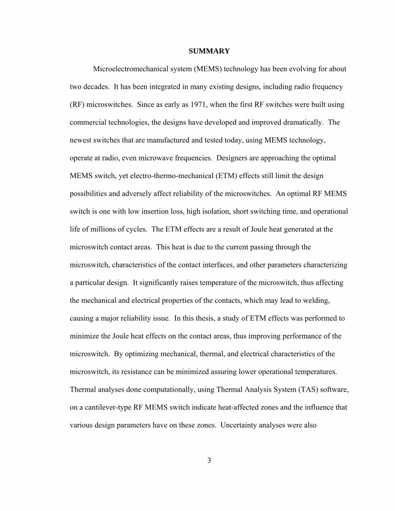
SUMMARY
Microelectromechanical system (MEMS) technology has been evolving for about
two decades. It has been integrated in many existing designs, including radio frequency
(RF) microswitches. Since as early as 1971, when the first RF switches were built using
commercial technologies, the designs have developed and improved dramatically. The
newest switches that are manufactured and tested today, using MEMS technology,
operate at radio, even microwave frequencies. Designers are approaching the optimal
MEMS switch, yet electro-thermo-mechanical (ETM) effects still limit the design
possibilities and adversely affect reliability of the microswitches. An optimal RF MEMS
switch is one with low insertion loss, high isolation, short switching time, and operational
life of millions of cycles. The ETM effects are a result of Joule heat generated at the
microswitch contact areas. This heat is due to the current passing through the
microswitch, characteristics of the contact interfaces, and other parameters characterizing
a particular design. It significantly raises temperature of the microswitch, thus affecting
the mechanical and electrical properties of the contacts, which may lead to welding,
causing a major reliability issue. In this thesis, a study of ETM effects was performed to
minimize the Joule heat effects on the contact areas, thus improving performance of the
microswitch. By optimizing mechanical, thermal, and electrical characteristics of the
microswitch, its resistance can be minimized assuring lower operational temperatures.
Thermal analyses done computationally, using Thermal Analysis System (TAS) software,
on a cantilever-type RF MEMS switch indicate heat-affected zones and the influence that
various design parameters have on these zones. Uncertainty analyses were also

4
performed to determine how good the results are. Based on the results obtained, for the
cases of the baseline design of the microswitch, considered in this thesis, contact
temperatures on the order of 700ºC were obtained. Although these temperatures are well
below the melting temperatures of the materials used, new designs of the microswitches
will have to be developed, in order to lower their maximum operating temperatures and
reduce temporal effects they cause, to increase reliability of the RF MEMS switches.
Results obtained in this thesis also showed that a microswitch with contact resistance
equal to 50% of that in the baseline design achieves maximum temperatures of 409ºC
leading to a higher operational reliability than that of the baseline design of the
microswitch.

5
ACKNOWLEDGEMENTS
This thesis was completed thanks to help of Prof. Ryszard J. Pryputniewicz. His
inspiration, advice, and support were endless. Special thanks also go to Prof. Cosme
Furlong and Prof. Joseph J. Rencis, the faculty of Mechanical Engineering Department,
for their assistance in completing this thesis; James R. Reid and Lavern A. Starman for
being a sea of RF MEMS knowledge; and David A. Rosato of Harvard Thermal for his
never ending aid with TAS modeling.

6
TABLE OF CONTENTS
Copyright 2
Summary 3
Acknowledgements 5
Table of contents 6
List of figures 8
List of tables 16
Nomenclature 17
Objectives 20
1. Introduction 21 1.1. Microswitch classification 22 1.2. Manufacturing process 28 1.3. Manufacturing challenges 33 1.4. Contact characteristics 35
1.4.1. Contact interface 35 1.4.2. Contact material 39
1.4.2.1. Pure metals 40 1.4.2.2. Alloys 41
1.4.3. Anti-stiction coating 42 1.4.4. Contact resistance 42
1.5. Integrated circuits 45
2. RF MEMS switch considered 47
3. Methodology 51 3.1. Analytical methods 51
3.1.1. Mechanical performance 52 3.1.1.1. Cantilever deformations 55
3.1.2. Thermal analysis 62 3.1.3. Maximum microswitch temperature 67
3.2. Computational methods 69 3.2.1. Mechanical analysis 69
3.2.1.1. Pro/ENGINEER model 69 3.2.1.2. Pro/MECHANICA algorithms 72
3.2.2. TAS analysis 74
7
3.2.2.1. TAS model 74 3.2.2.2. TAS algorithms 75
3.3. Uncertainty analysis 77 3.4. RF circuit analysis 79 3.5. Experimental methods 85
4. Results and discussion 92 4.1. Analytical results 92
4.1.1. Deformations 92 4.1.2. Temperature 97
4.2. Computational results 98 4.2.1. Deformations 98 4.2.2. Temperature 99
4.3. Uncertainty analysis 106 4.4. Circuit performance 112 4.5. Experimental images 113
5. Conclusions and future work 119
References 123
Appendix A. Analysis of deformations of the cantilever 128
Appendix B. Calculations of temperature 159
Appendix C. Uncertainty analysis 166
Appendix D. Analysis of RF circuit 184
8
LIST OF FIGURES
Fig. 1.1. A direct contact RF microswitch: (a) longitudinal cross section, (b) top view. 23
Fig. 1.2. Top view of a sample contact RF microswitch. 23
Fig. 1.3. A capacitive RF microswitch: (a) longitudinal cross section, (b) top view. 24
Fig. 1.4. Sample capacitive RF microswitch. 24
Fig. 1.5. Graphical representation of the Coulomb’s law. 25
Fig. 1.6. Magnetically induced force between two parallel wires. 26
Fig. 1.7. Linear thermal expansion of a solid. 27
Fig. 1.8. Series circuit configuration. 27
Fig. 1.9. Shunt circuit configuration. 28
Fig. 1.10. Single pole three throw circuit configuration. 28
Fig. 1.11. Anisotropic wet etching of bulk micromachining. 29
Fig. 1.12. Surface micromachining process overview. 31
Fig. 1.13. LIGA process overview. 32
Fig. 1.14. Phase diagram for supercritical drying. 34
Fig. 1.15. Crystal lattice impurities. 34
Fig. 1.16. Representative magnified contact surface. 36
Fig. 1.17. Material transfer at a contact. 37
Fig. 1.18. Illustration of (i) adhesively bonded contacts and (ii) material wear after application of tangential force: (a) adhesive wear, (b) burnishing wear. 38
Fig. 1.19. Sequence of reaction steps in the CVD process. 39
Fig. 1.20. Schematic illustration of an electroplating cell. 39

9
Fig. 1.21. Deformed asperity. 43
Fig. 1.22. Holm radius representation. 45
Fig. 1.23. Sample RC circuit. 46
Fig. 2.1. Cronos cantilever-type contact RF MEMS switch. 47
Fig. 2.2. Geometry and dimensions of the RF MEMS switch: (a) cross section, (b) top view. 48
Fig. 3.1. Configuration of the ACES methodology. 51
Fig. 3.2. One-dimensional model of the RF MEMS microswitch (Reid and Startman, 2003). 53
Fig. 3.3. Equivalent free body diagram for the cantilever beam. 53
Fig. 3.4. Deformations of electrostatically actuated cantilever: (a) at the beginning of actuation (zero deformation), (b) at the end of actuation (maximum deformation). 56
Fig. 3.5. Area in yz plane. 57
Fig. 3.6. Cross sectional area indicating axis of bending. 58
Fig. 3.7. The fixed-simply supported cantilever. 60
Fig. 3.8. Current flow through the microswitch contact areas. 63
Fig. 3.9. Contact resistance in conduction. 66
Fig. 3.10. Temperature distribution across an interface. 67
Fig. 3.11. Geometry and dimensions of the RF microswitch: (a) cross section, (b) top view. 70
Fig. 3.12. CAD model of the cantilever-type microswitch. 71
Fig. 3.13. TAS model of the cantilever-type microswitch. 74
Fig. 3.14. Gaussian distribution of the probability values. 78
Fig. 3.15. Two port RF circuit in series configuration. 79
Fig. 3.16. Circuit model of the RF MEMS switch in open position. 81

10
Fig. 3.17. Circuit model of the RF MEMS switch in closed position. 83
Fig. 3.18. Complete circuit based on RF MEMS switch. 84
Fig. 3.19. OELIM setup. 86
Fig. 3.20. Schematic of the OELIM configuration. 87
Fig. 3.21. Optical configuration of the OELIM setup. 91
Fig. 4.1. Cantilever deformations as a function of position along the microswitch, at the instant of the contact gap closure, for the electrostatic force of 6.44 µN. 93
Fig. 4.2. Slope as a function of position along the microswitch, at the instant of the contact gap closure. 93
Fig. 4.3. Cantilever deformations as a function of position along the microswitch, at the instant of the gap closure, including positional differences between the fixed and contact ends of the cantilever, for the electrostatic force of 6.44 µN. 94
Fig. 4.4. Slope as a function of position along the microswitch, at the instant of the contact gap closure, including positional differences between the fixed and contact ends of the cantilever. 95
Fig. 4.5. Cantilever deformations as a function of position along the microswitch, where F1 is the nominal force value, F2 is twice that value, F3 is three times that value, and F4 is four times the nominal force value. 96
Fig. 4.6. Slip force as a function of coefficient of friction and normal force for F1, F2, F3 and F4. 97
Fig. 4.7. Cantilever deformations (in mm) based on Pro/MECHANICA analysis. 99
Fig. 4.8. Overall RF MEMS switch temperature distribution excluding convection and radiation. 101
Fig. 4.9. Detail of the contact temperature distribution excluding convection and radiation. 101
Fig. 4.10. Overall RF MEMS switch temperature distribution including convection and radiation. 102

11
Fig. 4.11. Detail of the cantilever and shorting bar temperature distribution including convection and radiation. 102
Fig. 4.12. Detail of the contact temperature distribution including convection and radiation. 103
Fig. 4.13. Detail of the temperature distribution within the Joule heat affected zones of the shorting bar at the contact areas including convection and radiation. 104
Fig. 4.14. Detail of the shorting bar temperature distribution including convection and radiation. 104
Fig. 4.15. Substrate temperature distribution including convection and radiation. 105
Fig. 4.16. Overall RF MEMS switch temperature distribution including convection and radiation, using a 50% lower contact resistance. 106
Fig. 4.17. Overall uncertainty in deformations of section-1 of the cantilever as a function of position along the microswitch. 108
Fig. 4.18. Percent overall uncertainty in deformations of section-1 of the cantilever as a function of position along the microswitch. 108
Fig. 4.19. Percent contributions of uncertainties in individual parameters to the overall uncertainty in deformations of section-1 of the cantilever as a function of position along the microswitch on a lin-lin scale. 109
Fig. 4.20. Percent contributions of uncertainties in individual parameters to the overall uncertainty in deformations of section-1 of the cantilever as a function of position along the microswitch on a lin-log scale. 109
Fig. 4.21. Overall uncertainty in deformations of section-2 of the cantilever as a function of position along the microswitch. 110
Fig. 4.22. Percent overall uncertainty in deformations of section-2 of the cantilever as a function of position along the microswitch. 110
Fig. 4.23. Percent contributions of uncertainties in individual parameters to the overall uncertainty in deformations of section-2 of the cantilever as a function of position along the microswitch on a lin-lin scale. 111
12
Fig. 4.24. Percent contributions of uncertainties in individual parameters to the overall uncertainty in deformations of section-2 of the cantilever as a function of position along the microswitch on a lin-log scale. 111
Fig. 4.25. Isolation of the RF microswitch as a function of its operational frequency. 112
Fig. 4.26. Insertion loss of the RF microswitch as a function of its operational frequency. 113
Fig. 4.27. Unreleased die containing multiple RF MEMS components, 5 mm × 5 mm. 114
Fig. 4.28. Detail of the unreleased die, highlighted in Fig. 4.27. 115
Fig. 4.29. Unreleased cantilever-type RF MEMS switches of variable width, highlighted in Fig. 4.28. 116
Fig. 4.30. Unreleased cantilever type RF MEMS switch, highlighted in Fig. 4.29, 200 µm long and 18 µm wide. 116
Fig. 4.31. Sample phase shifted image of the RF MEMS switches. 117
Fig. 4.32. Wrapped phase map of the RF MEMS switches. 117
Fig. 4.33. OELIM determined deformations of a section of die containing representative RF MEMS contact switches. 118
Fig. A.1. RF MEMS cantilever-type microswitch considered in this thesis. 129
Fig. A.2. Deformations of electrostatically actuated cantilever: (a) at the beginning of actuation (zero deformation), (b) at the end of actuation (maximum deformation). 131
Fig. A.3. Free-body diagram of section-1 of the cantilever. 132
Fig. A.4. Free-body diagram of section-1 of the cantilever at an arbitrary distance x. 133
Fig. A.5. Deformations of section-1 of the cantilever as a function of position along the microswitch. 137
Fig. A.6. Slope of section-1 of the cantilever as a function of position along the microswitch. 137
13
Fig. A.7. Deformations of section-2 of the cantilever as a function of position along the microswitch. 138
Fig. A.8. Slope of section-2 of the cantilever as a function of position along the microswitch. 139
Fig. A.9. Deformations of the entire cantilever as a function of position along the microswitch. 139
Fig. A.10. Slope of the entire cantilever as a function of position along the microswitch. 140
Fig. A.11. Free-body diagram of a fixed-simply supported cantilever, after contact is made. 140
Fig. A.12. Free-body diagram of section-1 of the cantilever, after contact is made. 142
Fig. A.13. Free-body diagram of section-2 of the cantilever, after contact is made. 143
Fig. A.14. Deformations of section-1 of the cantilever as a function of position along the microswitch, after contact is made. 146
Fig. A.15. Slope of section-1 of the cantilever as a function of position along the microswitch, after contact is made. 146
Fig. A.16. Deformations of section-2 of the cantilever as a function of position along the microswitch, after contact is made. 147
Fig. A.17. Slope of section-2 of the cantilever as a function of position along the microswitch, after contact is made. 147
Fig. A.18. Deformations of the entire cantilever as a function of position along the microswitch, after contact is made. 148
Fig. A.19. Slope of the entire cantilever as a function of position along the microswitch, after contact is made. 148
Fig. A.20. Deformations of section-1 of the cantilever as a function of position along the microswitch, after contact is made by closing the gap dg = 1µm. 150
Fig. A.21. Slope of section-1 of the cantilever as a function of position along the microswitch, after contact is made by closing the gap dg = 1µm. 150
14
Fig. A.22. Deformations of section-2 of the cantilever as a function of position along the microswitch, after contact is made by closing the gap dg = 1µm. 151
Fig. A.23. Slope of section-2 of the cantilever as a function of position along the microswitch, after contact is made by closing the gap dg = 1µm. 151
Fig. A.24. Deformations of the entire cantilever as a function of position along the microswitch, after contact is made by closing the gap dg = 1µm. 152
Fig. A.25. Slope of the entire cantilever as a function of position along the microswitch, after contact is made by closing the gap dg = 1µm. 152
Fig. A.26. Deformations of the cantilever as functions of position along the microswitch, after contact is made by closing the gap dg = 1µm, for different magnitudes of the actuation force. 155
Fig. A.27. Slip force at the end of the cantilever. 156
Fig. A.28. Slip forces as functions of coefficient of friction for F1, F2, F3, and F4. 157
Fig. C.1. Overall uncertainty in deformations of section-1 of the cantilever as a function of position along the microswitch. 175
Fig. C.2. Percent overall uncertainty in deformations of section-1 of the cantilever as a function of position along the microswitch. 175
Fig. C.3. Percent contributions of individual uncertainties to overall uncertainty in deformations of section-1 of the cantilever as a function of position along the microswitch, lin-lin scale. 177
Fig. C.4. Percent contributions of individual uncertainties to overall uncertainty in deformations of section-1 of the cantilever as a function of position along the microswitch, lin-log scale. 177
Fig. C.5. Overall uncertainty in deformations of section-2 of the cantilever as a function of position along the microswitch. 178
Fig. C.6. Percent overall uncertainty in deformations of section-2 of the cantilever as a function of position along the microswitch. 180
15
Fig. C.7. Percent contributions of individual uncertainties to overall uncertainty in deformations of section-2 of the cantilever as a function of position along the microswitch, lin-lin scale. 182
Fig. C.8. Percent contributions of individual uncertainties to overall uncertainty in deformations of section-2 of the cantilever as a function of position along the microswitch, lin-log scale 182
Fig. D.1. Circuit of the RF MEMS switch in open position. 186
Fig. D.2. Impedance of the open microswitch as a function of its operational frequency. 187
Fig. D.3. Circuit of the RF MEMS switch in closed position. 188
Fig. D.4. Impedance of closed microswitch as a function of its operational frequency. 189
Fig. D.5. Schematic of the RF circuit impedance. 189
Fig. D.6. Microswitch isolation in decibels as a function of frequency. 191
Fig. D.7. Microswitch insertion loss in decibels as a function of frequency. 191
16
LIST OF TABLES
Table 1.1. Common surface micromachining materials. 30
Table 1.2. Characteristics of various contact materials. 40
Table 2.1. Dimensions of the RF MEMS switch, Fig. 2.2. 49
Table 2.2. Material properties of polysilicon. 49
Table 3.1. The Lorenz numbers for common metals. 68
Table 3.2. Values of logee for self inductance calculations. 83

17
NOMENCLATURE
a average contact asperity radius b width of cantilever be width of electrode bs width of shorting bar bt width of trace cp specific heat d distance, damping coefficient dc average center to center distance between asperities de distance between electrodes dg contact gap do height of the cantilever post fo fundamental natural frequency g gravitational acceleration h cantilever thickness, convective heat transfer coefficient hc contact coefficient hs shorting bar thickness ht trace thickness i1,2 current in the circuit j 1− k constant, spring constant, thermal conductivity kA thermal conductivity of material A kB thermal conductivity of material B m dynamic mass n number of asperities per unit area pm maximum contact pressure w geometric constant x distance x1 axial position along section-1 of the cantilever x2 axial position along section-2 of the cantilever A area AA cross-sectional area of material A AB cross-sectional area of material B Ac contact area, area through which heat convection occurs Ak area through which heat conduction occurs Ar radiation area B bias limit C electrical capacitance, integration constant D depth, diameter E modulus of elasticity F force FES electrostatic force

18
Fk spring force Fn normal force Fs geometric view factor, sliding force FS slip force Gr Grashof number H material hardness I current, second moment of area K vector L length, electrical inductance L vector L1 length of section-1 of the cantilever L2 length of section-2 of the cantilever Lc length of contact Le length of electrodes Lo horizontal distance from the cantilever post to the electrode Lr Lorenz number Ls length of shorting bar Lt length of traces Lto discontinuity in trace under shorting bar M bending moment N isoparametric element Ni shape function Nu Nusselt number Pj Legendre polynomial PX precision limit Pr Prandtl number Q electric charge Qc heat transfer due to convection Qi electric charge QJ Joule heat Qk heat transfer due to conduction Qr heat transfer due to radiation R radius, electrical resistance RA reaction force Rc thermal resistance due to convection, thermal contact resistance RC electrical contact resistance RE electrical resistance of a conductor Rk thermal resistance due to conduction Rr thermal resistance due to radiation SX precision index T temperature T1 beginning temperature, temperature of node 1 T2 end temperature, temperature of node 2 Te temperature of enclosure

19
Ts temperature of surface T∞ ambient temperature UX uncertainty value V voltage, volume V1,2 voltage present in a circuit VG voltage supplied to the RF circuit VZ voltage in the RF circuit X single value parameter X mean value of a variable Y yield coefficient Z electrical impedance Zo electrical impedance of the circuit Zopen electrical impedance of open microswitch Zclosed electrical impedance of closed microswitch α Holm radius αT coefficient of thermal expansion β volume coefficient of expansion δX RSS uncertainty εo dielectric constant of air εr relative permittivity εs emissivity of surface µ friction coefficient µo permeability of free space ν kinematic viscosity ρ material density ρe electrical resistivity ρcpV thermal capacitance σ Stefan-Boltzmann constant, standard deviation σy yield strength ω electrical current frequency ξ local position along the element studied ζ asperity deformation ζc critical asperity deformation ∆ distance between nodes ∆t time increment ∆T temperature change Ω fringe-locus function

20
OBJECTIVES
The objectives of this thesis were to study Joule heat effects on operation of RF
MEMS switches, in order to identify factors which may increase their overall operational
reliability, using analytical, computational, and experimental solutions (ACES)
methodology.
21
1. INTRODUCTION
Microelectromechanical systems (MEMS) have been developing with time,
following the trends in technology and assimilating to the market demands. Petersen
(1979) was a pioneer of frequency switches, although his switch was not a part of what
we now refer to as MEMS. His research for IBM Corporation was a foundation for work
of researchers like Yao and Chang (1995), or Brown (1998), who brought down the size
of the original switch to microscale. As the technology evolved, so did the MEMS
designs. The first Petersen cantilever-type switch working at low frequencies has now
advanced to tunable microswitches working at radio, even microwave frequencies (Li, et
al., 1999; Zou, et al., 2000).
MEMS devices are currently used in telecommunications, wireless networking,
global positioning systems, cellular, auto, and even toy industry (De Los Santos and
Richards, 2001). Microcomponents greatly reduce size and weight of many products,
while reducing their cost and improving performance (Pryputniewicz and Furlong, 2002).
Although, at this time, MEMS bring large number of advantages to a range of industries
much can still be done to improve their reliability.
Microswitches are an important part of all MEMS devices. These microswitches
fit two major design groups: capacitive and resistive (Pryputniewicz, et al., 2002a,
2002b). The capacitive design of a microswitch refers to membrane type microswitches
that use difference in capacitance between two electrodes as means of actuation.
Resistive, or contact, cantilever type microswitches use electrostatic force as means of
actuating the switch and consequently making a metal-to-metal contact.
22
Contact MEMS switches present a major reliability concern. The Joule heat
generated when the current is passed through the microswitch causes its temperature to
reach hundreds of degrees Celsius which, in turn, makes the contacts to wear at an
increased rate or, at the extreme, weld. Changing certain design parameters, e.g.,
materials, dimensions, and/or surface finish of contacts, can enhance the life of the
microswitch. Modifying the integrated circuits (ICs) featuring the microswitches has
been proven as a successful technique for decreasing the current passing through the
microswitch, thus may be used as another promising method of improving the
microswitch reliability (Tyco 2000a).
1.1. Microswitch classification
The radio frequency (RF) MEMS switches can be categorized based on the
contact type, actuation method, and configuration. The two types of contacts present in
RF MEMS switch designs are the metal to metal contacts and metal-insulator-metal
contacts. The metal to metal contacts, also referred to as ohmic or direct contacts, can be
found in cantilever-type MEMS switches. The signal in this microswitch is propagated
when the two metal contacts come together and electrical current passes through the
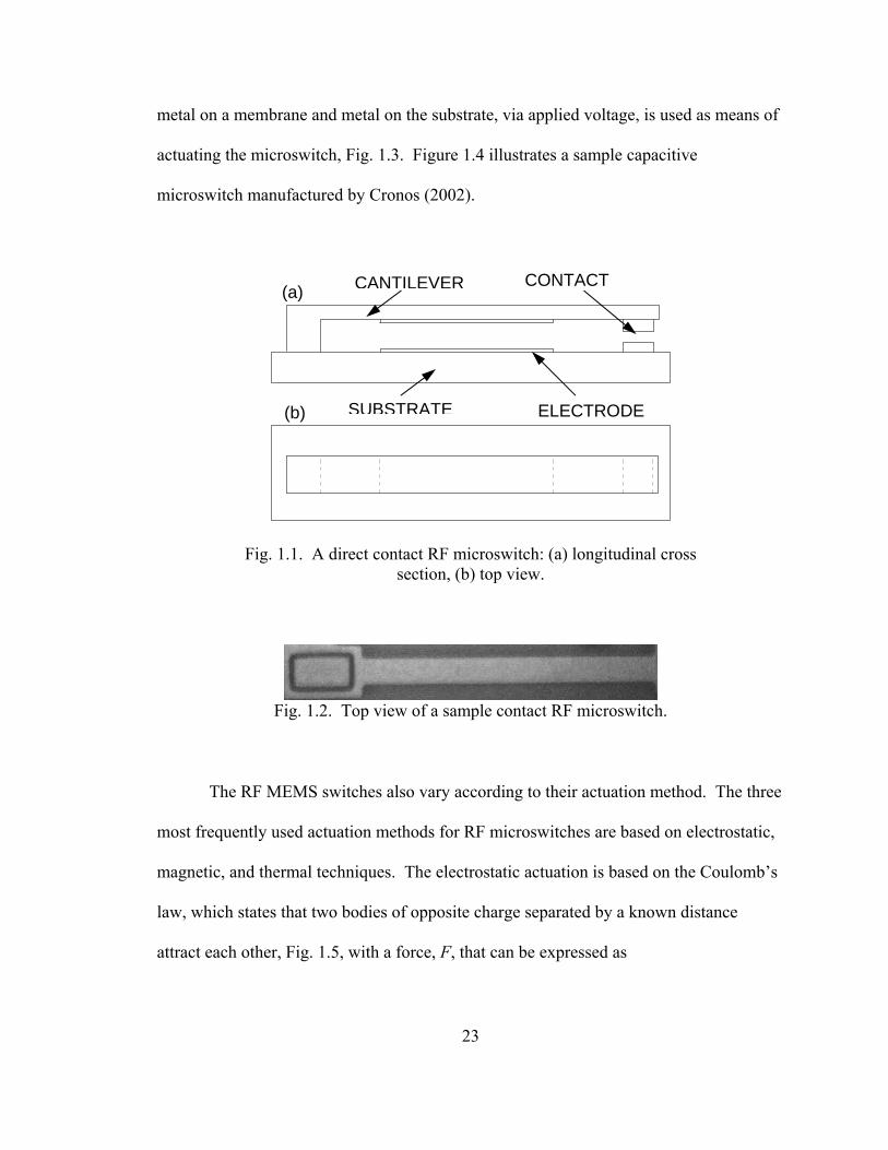
established interface, Fig. 1.1. A sample cantilever-type microswitch manufactured by
Cronos (2002) is shown in Fig. 1.2.
The metal-insulator-metal contacts, sometimes referred to as capacitive or indirect
contacts, are found in membrane microswitches. The capacitance built up between the
23
metal on a membrane and metal on the substrate, via applied voltage, is used as means of
actuating the microswitch, Fig. 1.3. Figure 1.4 illustrates a sample capacitive
microswitch manufactured by Cronos (2002).
Fig. 1.1. A direct contact RF microswitch: (a) longitudinal cross
section, (b) top view.
Fig. 1.2. Top view of a sample contact RF microswitch.
The RF MEMS switches also vary according to their actuation method. The three
most frequently used actuation methods for RF microswitches are based on electrostatic,
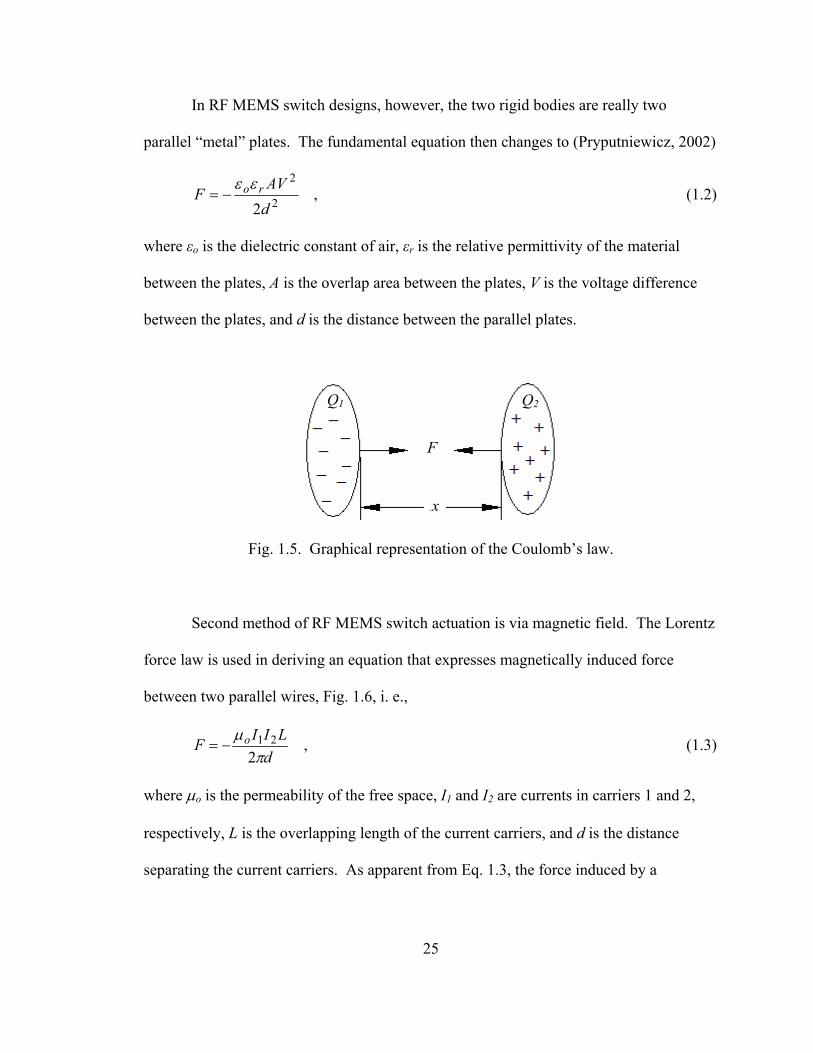
magnetic, and thermal techniques. The electrostatic actuation is based on the Coulomb’s
law, which states that two bodies of opposite charge separated by a known distance
attract each other, Fig. 1.5, with a force, F, that can be expressed as
(a)
(b)
CANTILEVER
SUBSTRATE
CONTACT
ELECTRODE

24
,221
xQQkF = (1.1)
where k is a constant, Q1 and Q2 are electric charges, and x is the distance separating the
charges.
Fig. 1.3. A capacitive RF microswitch: (a) longitudinal cross section,
(b) top view.
Fig. 1.4. Sample capacitive RF microswitch.
MEMBRANE
(b)
(a)
SUBSTRATE ELECTRODE
25
In RF MEMS switch designs, however, the two rigid bodies are really two
parallel “metal” plates. The fundamental equation then changes to (Pryputniewicz, 2002)
,2 2
2
dAV
F roεε−= (1.2)
where εo is the dielectric constant of air, εr is the relative permittivity of the material
between the plates, A is the overlap area between the plates, V is the voltage difference
between the plates, and d is the distance between the parallel plates.
Fig. 1.5. Graphical representation of the Coulomb’s law.
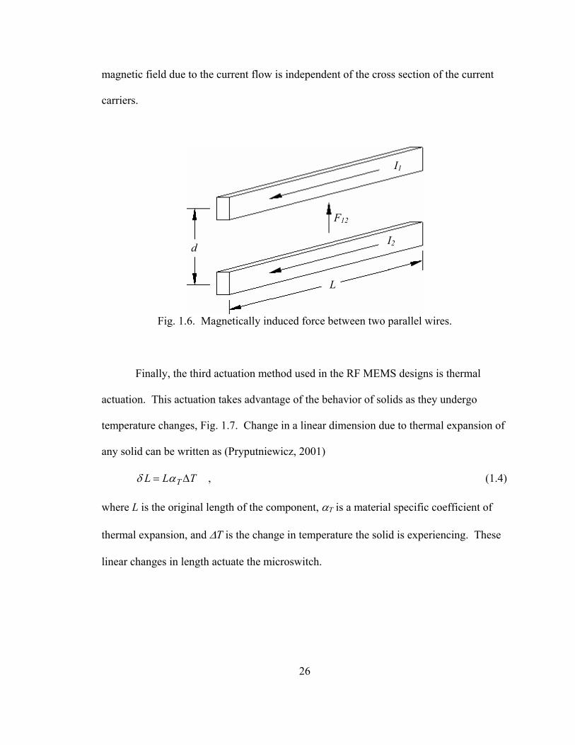
Second method of RF MEMS switch actuation is via magnetic field. The Lorentz
force law is used in deriving an equation that expresses magnetically induced force
between two parallel wires, Fig. 1.6, i. e.,
,2
21d
LIIF oπ
µ−= (1.3)
where µo is the permeability of the free space, I1 and I2 are currents in carriers 1 and 2,
respectively, L is the overlapping length of the current carriers, and d is the distance
separating the current carriers. As apparent from Eq. 1.3, the force induced by a
F
Q1
x
Q2
26
magnetic field due to the current flow is independent of the cross section of the current
carriers.
Fig. 1.6. Magnetically induced force between two parallel wires.
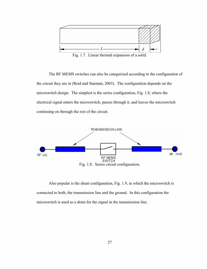
Finally, the third actuation method used in the RF MEMS designs is thermal
actuation. This actuation takes advantage of the behavior of solids as they undergo
temperature changes, Fig. 1.7. Change in a linear dimension due to thermal expansion of
any solid can be written as (Pryputniewicz, 2001)
,TLL T ∆= αδ (1.4)
where L is the original length of the component, αT is a material specific coefficient of
thermal expansion, and ∆T is the change in temperature the solid is experiencing. These
linear changes in length actuate the microswitch.
L
I1
I2d
F12
27
Fig. 1.7. Linear thermal expansion of a solid.
The RF MEMS switches can also be categorized according to the configuration of
the circuit they are in (Reid and Starman, 2003). The configuration depends on the
microswitch design. The simplest is the series configuration, Fig. 1.8, where the
electrical signal enters the microswitch, passes through it, and leaves the microswitch
continuing on through the rest of the circuit.
Fig. 1.8. Series circuit configuration.
Also popular is the shunt configuration, Fig. 1.9, in which the microswitch is
connected to both, the transmission line and the ground. In this configuration the
microswitch is used as a drain for the signal in the transmission line.
L δL δL δ
28
Fig. 1.9. Shunt circuit configuration.
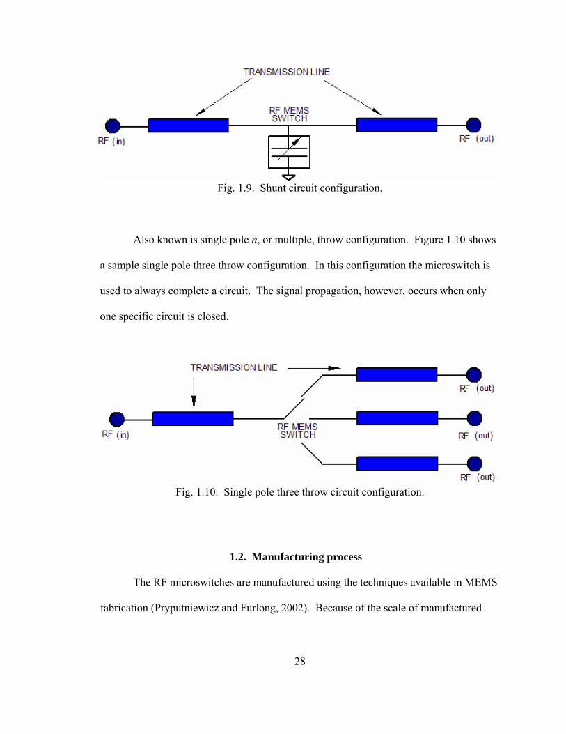
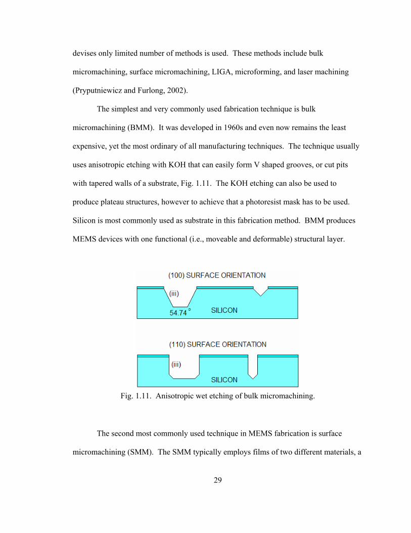
Also known is single pole n, or multiple, throw configuration. Figure 1.10 shows
a sample single pole three throw configuration. In this configuration the microswitch is
used to always complete a circuit. The signal propagation, however, occurs when only
one specific circuit is closed.
Fig. 1.10. Single pole three throw circuit configuration.
1.2. Manufacturing process
The RF microswitches are manufactured using the techniques available in MEMS
fabrication (Pryputniewicz and Furlong, 2002). Because of the scale of manufactured
29
devises only limited number of methods is used. These methods include bulk
micromachining, surface micromachining, LIGA, microforming, and laser machining
(Pryputniewicz and Furlong, 2002).
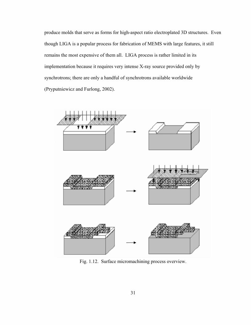
The simplest and very commonly used fabrication technique is bulk
micromachining (BMM). It was developed in 1960s and even now remains the least
expensive, yet the most ordinary of all manufacturing techniques. The technique usually
uses anisotropic etching with KOH that can easily form V shaped grooves, or cut pits
with tapered walls of a substrate, Fig. 1.11. The KOH etching can also be used to
produce plateau structures, however to achieve that a photoresist mask has to be used.
Silicon is most commonly used as substrate in this fabrication method. BMM produces
MEMS devices with one functional (i.e., moveable and deformable) structural layer.
Fig. 1.11. Anisotropic wet etching of bulk micromachining.
The second most commonly used technique in MEMS fabrication is surface
micromachining (SMM). The SMM typically employs films of two different materials, a

30
structural material (e.g., polysilicon) and a sacrificial material (e.g., silicon dioxide,
commonly referred to as oxide), Table 1.1. The layers are deposited, patterned, and
removed by wet etching to release the structure (Pryputniewicz, 2002). An example of
surface micromachining is presented in Fig. 1.12. The SMM holds a key advantage over
the BMM in that the SMM components can be one or two orders of magnitude smaller
than their BMM counterparts. Currently, the most advanced surface micromachining that
is successfully used involves five structural layers and was developed at Sandia National
Laboratories. This fabrication is known as Sandia’s Ultraplanar MEMS Multi-level
Technology (SUMMiT™V) (Pryputniewicz, 2002). This SUMMiT™V process is
capable of producing gears, hinges, and combdrives.
Table 1.1. Common surface micromachining materials.
Structural layers Sacrificial layers
Polysilicon SiO2 Al Polysilicon
Al / Au Polyimide / PMGI Au / Ni Copper
Si3N4 / Al / SiO2 Polysilicon
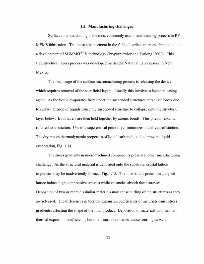
Another fabrication method for MEMS devices is LIGA. The acronym LIGA
comes from the German name for the process (Lithographie, Galvanoformung,
Abformung). LIGA uses lithography, electroplating, and molding processes to produce
millimeter sized devices, Fig. 1.13. In this technique X-ray lithography is used to
31
produce molds that serve as forms for high-aspect ratio electroplated 3D structures. Even
though LIGA is a popular process for fabrication of MEMS with large features, it still
remains the most expensive of them all. LIGA process is rather limited in its
implementation because it requires very intense X-ray source provided only by
synchrotrons; there are only a handful of synchrotrons available worldwide
(Pryputniewicz and Furlong, 2002).
Fig. 1.12. Surface micromachining process overview.

32
Also, MEMS devices with relatively large aspect ratios can be manufactured by
microforming. It is an extension of surface micromachining, however, unlike
micromachining it produces a high aspect ratio structures. Microforming uses
electroplating to form metal structures and the Multi-User MEMS Process (MUMPS) for
metals (Koester, el at., 2001).
In the University of Colorado project, laser machining was used to manufacture a
moveable microswitch membrane (Wang, et al., 2001). In this project the AVIA laser
with a wavelength of 355 nm and an excimer laser with a wavelength of 248 nm were
used to cut slots in Krypton-E copper cladding film. This laser technique, however,
causes thermal damages, unless appropriate materials and laser wavelengths are chosen.
Fig. 1.13. LIGA process overview.
33
1.3. Manufacturing challenges
Surface micromachining is the most commonly used manufacturing process in RF
MEMS fabrication. The latest advancement in the field of surface micromachining led to
a development of SUMMiTTMV technology (Pryputniewicz and Furlong, 2002). This
five structural layers process was developed by Sandia National Laboratories in New
Mexico.
The final stage of the surface micromachining process is releasing the device,
which requires removal of the sacrificial layers. Usually this involves a liquid releasing
agent. As the liquid evaporates from under the suspended structures attractive forces due
to surface tension of liquids cause the suspended structure to collapse onto the structural
layer below. Both layers are then held together by atomic bonds. This phenomenon is
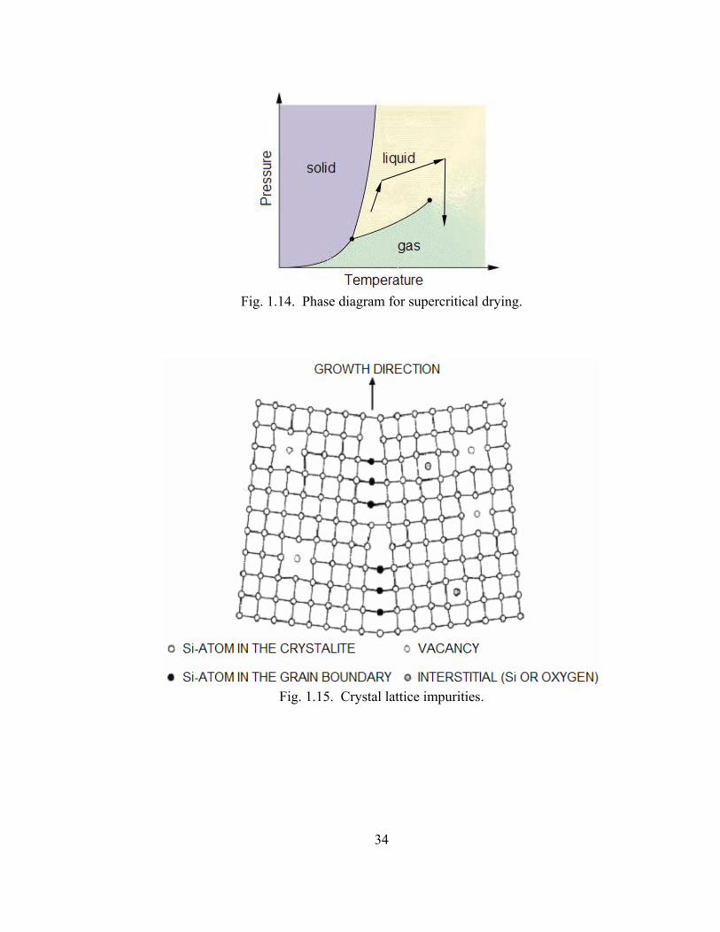
referred to as stiction. Use of a supercritical point dryer minimizes the effects of stiction.
The dryer uses thermodynamic properties of liquid carbon dioxide to prevent liquid
evaporation, Fig. 1.14.
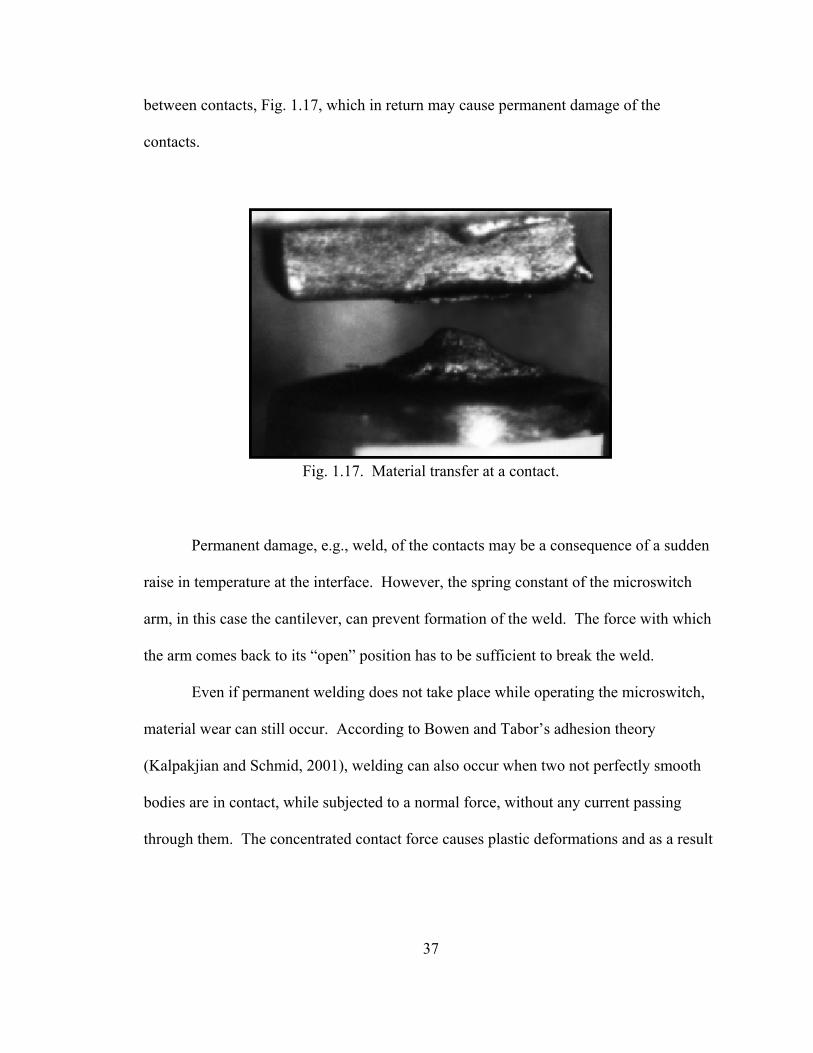
The stress gradients in micromachined components present another manufacturing
challenge. As the structural material is deposited onto the substrate, crystal lattice
impurities may be inadvertently formed, Fig. 1.15. The interstitials present in a crystal
lattice induce high compressive stresses while vacancies absorb these stresses.
Deposition of two or more dissimilar materials may cause curling of the structures as they
are released. The differences in thermal expansion coefficients of materials cause stress
gradients, affecting the shape of the final product. Deposition of materials with similar
thermal expansion coefficients, but of various thicknesses, causes curling as well.
34
Fig. 1.14. Phase diagram for supercritical drying.
Fig. 1.15. Crystal lattice impurities.

35
1.4. Contact characteristics
In order to improve the microswitch reliability, certain design parameters may
have to be changed or varied. The most important of those parameters is the actual
interface contact area of the microswitch, contact materials, and the interface resistance
between the contacts.
1.4.1. Contact interface
According to Tyco (2000b) and Mroczkowski (1998) when two switch contacts
are overlapped, or in contact, only a portion of their area is truly allowing electric current
flow. On a microscale, the surface of the contact material, which conducts electricity
across the interface, is not perfectly flat, but has many peaks and valleys, as shown in Fig.
1.16. For this reason, the electric current flows across the switch contact interface only
where the high points, or asperities, meet. The actual contact area may be substantially
smaller in comparison with the apparent contact area of the microswitch which was
intended by the designer.
The actual contact area, however, depends not only on the surface roughness of
the two contacting surfaces, but also on the contact force which is normal to the interface.
If this normal force is large enough, it can cause plastic deformations of the asperities,
thus increasing the actual contact area. The relationship between the actual contact area
and the contact force can be expressed as (Mroczkowski, 1998)

36
Fig. 1.16. Representative magnified contact surface.
,HF
kA nc = (1.5)
where Ac is the actual contact area, H is the hardness of contact material, Fn is the normal
force, and k is the proportionality constant. This constant depends on a number of
parameters including the effects of film, lubrication, surface roughness, contact force, and
the mode of deformation, among others.
Finally as the two contacts come together, only the highest peaks are subject to a
full current load. This causes a sudden raise in temperature and a “melt down” of those
peaks increasing the actual contact interface. This melting of the contact metal causes
superheating of the surrounding air and its ionization. With high enough voltage an arc
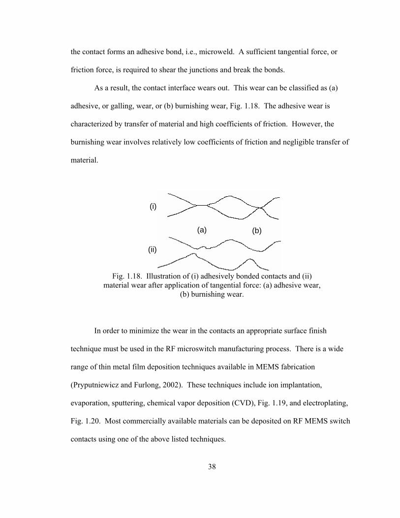
may generate. The melting of the contact material may also cause material transfer
37
between contacts, Fig. 1.17, which in return may cause permanent damage of the
contacts.
Fig. 1.17. Material transfer at a contact.
Permanent damage, e.g., weld, of the contacts may be a consequence of a sudden
raise in temperature at the interface. However, the spring constant of the microswitch
arm, in this case the cantilever, can prevent formation of the weld. The force with which
the arm comes back to its “open” position has to be sufficient to break the weld.
Even if permanent welding does not take place while operating the microswitch,
material wear can still occur. According to Bowen and Tabor’s adhesion theory
(Kalpakjian and Schmid, 2001), welding can also occur when two not perfectly smooth
bodies are in contact, while subjected to a normal force, without any current passing
through them. The concentrated contact force causes plastic deformations and as a result
38
the contact forms an adhesive bond, i.e., microweld. A sufficient tangential force, or
friction force, is required to shear the junctions and break the bonds.
As a result, the contact interface wears out. This wear can be classified as (a)
adhesive, or galling, wear, or (b) burnishing wear, Fig. 1.18. The adhesive wear is
characterized by transfer of material and high coefficients of friction. However, the
burnishing wear involves relatively low coefficients of friction and negligible transfer of
material.
Fig. 1.18. Illustration of (i) adhesively bonded contacts and (ii)
material wear after application of tangential force: (a) adhesive wear, (b) burnishing wear.
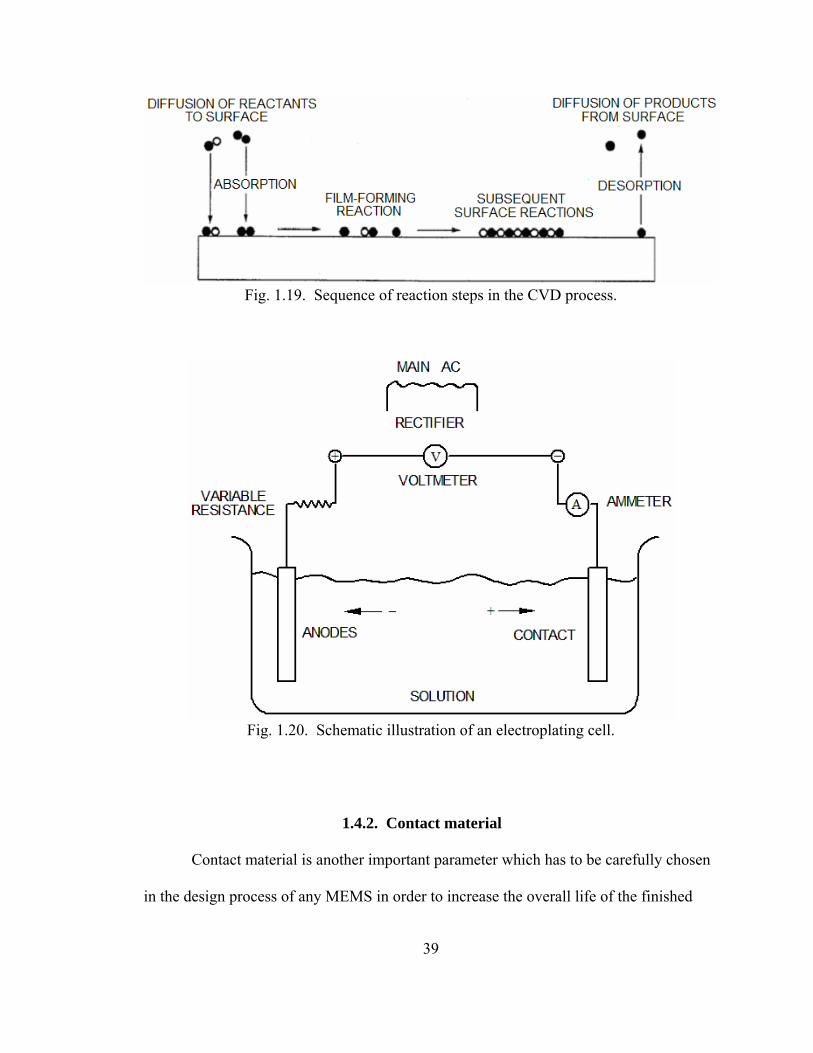
In order to minimize the wear in the contacts an appropriate surface finish
technique must be used in the RF microswitch manufacturing process. There is a wide
range of thin metal film deposition techniques available in MEMS fabrication
(Pryputniewicz and Furlong, 2002). These techniques include ion implantation,
evaporation, sputtering, chemical vapor deposition (CVD), Fig. 1.19, and electroplating,
Fig. 1.20. Most commercially available materials can be deposited on RF MEMS switch
contacts using one of the above listed techniques.
(a) (b)
(i)
(ii)
39
Fig. 1.19. Sequence of reaction steps in the CVD process.
Fig. 1.20. Schematic illustration of an electroplating cell.
1.4.2. Contact material
Contact material is another important parameter which has to be carefully chosen
in the design process of any MEMS in order to increase the overall life of the finished

40
device. Most often metals are chosen as the contact material, each metal however, with
its unique properties can greatly affect the microswitch reliability. Table 1.2 (Tyco,
2000a) summarizes some contact metal characteristics, which are also described in detail
in Sections 1.4.2.1 and 1.4.2.2.
Table 1.2. Characteristics of various contact materials.
Material Electrical
conductivity %IACS
Arc voltage
Arc current
Cadmium 24 10 0.5 Silver 105 12 0.4 Gold 77 15 0.38 Copper 100 13 0.43 Nickel 25 14 0.5 Palladium 16 15 0.5 Tungsten 31 15 1.0
1.4.2.1. Pure metals
Fine silver has the best electrical and thermal properties of all metals.
Unfortunately, silver is affected by sulfidation of about 70 micrograms per square
centimeter per day (Tyco 2000a). Sulfidation forms a film on the contact surface which
increases the interface resistance. The sulfidation film has also been known to capture
airborne dirt particles. The wiping, or contact, force of the closing microswitch has to be
large enough to break through the formed film in order to create a good electrical contact
(Pryputniewicz, et al., 2001a).
Gold flashing on each of the contacts results in almost no sulfidation at all and
provides good electrical conductivity. Gold also does not oxidize, assuring always
41
conducting contact area. However, due to low melting temperature, gold has tendency of
coming off the contact if it is in an environment at temperatures above 350˚C.
Palladium contacts do not oxidize or sulfidate, but have a very low electrical
conductivity. The palladium life is ten times that of fine silver, which makes it a good
choice for a contact from the reliability stand point.
1.4.2.2. Alloys
Silver alloyed with 0.15% nickel gives the contact a fine grain structure. As a
result the material transfer from one contact to another is more evenly distributed, thus
delaying contact failure.
Silver cadmium oxide is much more resistant to material transfer and material loss
due to arcing than fine silver, but is much less electrically conductive. This alloy also has
a higher interface resistance and a greater contact assembly heat rise. Like fine silver it
will both oxidize and sulfidate with time.
Although it is very rare, silver tin indium oxide exhibits better resistance to arc
erosion and welding than silver cadmium alloy. Silver tin indium is less electrically
conductive, even though it is harder than silver cadmium. It also has a greater interface
resistance, thus greater voltage drop and a heat rise.
42
1.4.3. Anti-stiction coating
Stiction presents a major problem in microswitch design. The in-use-stiction, one
that occurs when parts come into contact, causes permanent collapse of the designed
structure. The capillary, electrostatic, and van der Waals forces are primarily responsible
for this stiction. Capillary and electrostatic forces can be eliminated by treating the
surfaces and making them hydrophobic. The Self-Assembly Monolayer (SAM) coating
dramatically reduces stiction due to the capillary and electrostatic forces, while reducing
friction and wear (Maboudian, el al., 2000). The van der Waals forces, however, can
only be reduced by roughening the surfaces. Unfortunately this further reduces the
contact area between the electrodes increasing the Joule heat effect.
1.4.4. Contact resistance
Much work has been done to model contact areas and their interface. Works of
Greenwood (1966), Greenwood and Williamson (1966), Chang, el al. (1987), and
Bhushan (1996, 1998) show much attempt in finding methods to describe mathematically
the actual areas that come in contact when two surfaces make an intimate interface. The
interface conductance and resistance depend on the actual contact area.
A thorough investigation done by University of California at Berkeley (Chang, et
al., 1987) incorporated both elastic and plastic deformations of contacting asperities.
Asperity deformation, ζ, Fig. 1.21, due to applied pressure can be calculated as
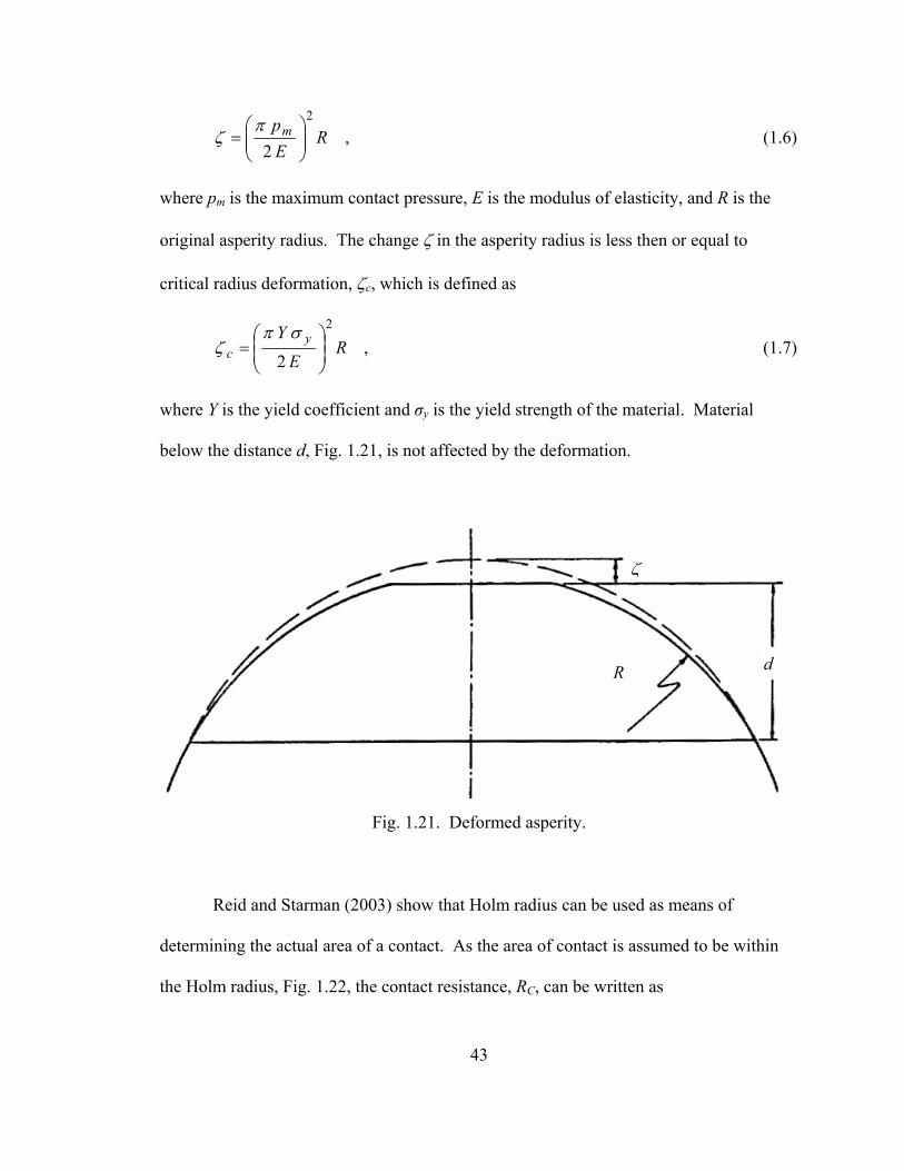
43
,2
2
REpm
⎟⎟⎠
⎞⎜⎜⎝
⎛=
πζ (1.6)
where pm is the maximum contact pressure, E is the modulus of elasticity, and R is the
original asperity radius. The change ζ in the asperity radius is less then or equal to
critical radius deformation, ζc, which is defined as
,2
2
RE
Y yc ⎟⎟
⎠
⎞⎜⎜⎝
⎛=
σπζ (1.7)
where Y is the yield coefficient and σy is the yield strength of the material. Material
below the distance d, Fig. 1.21, is not affected by the deformation.
Fig. 1.21. Deformed asperity.
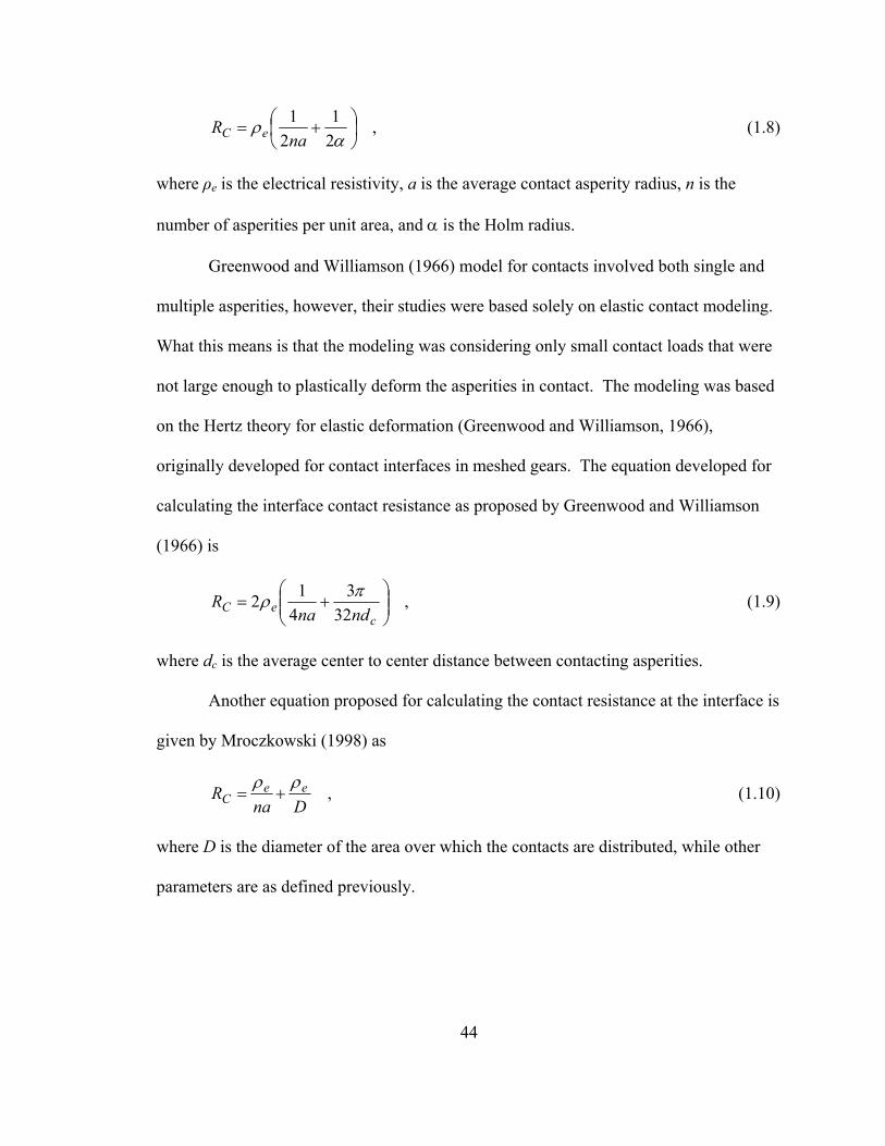
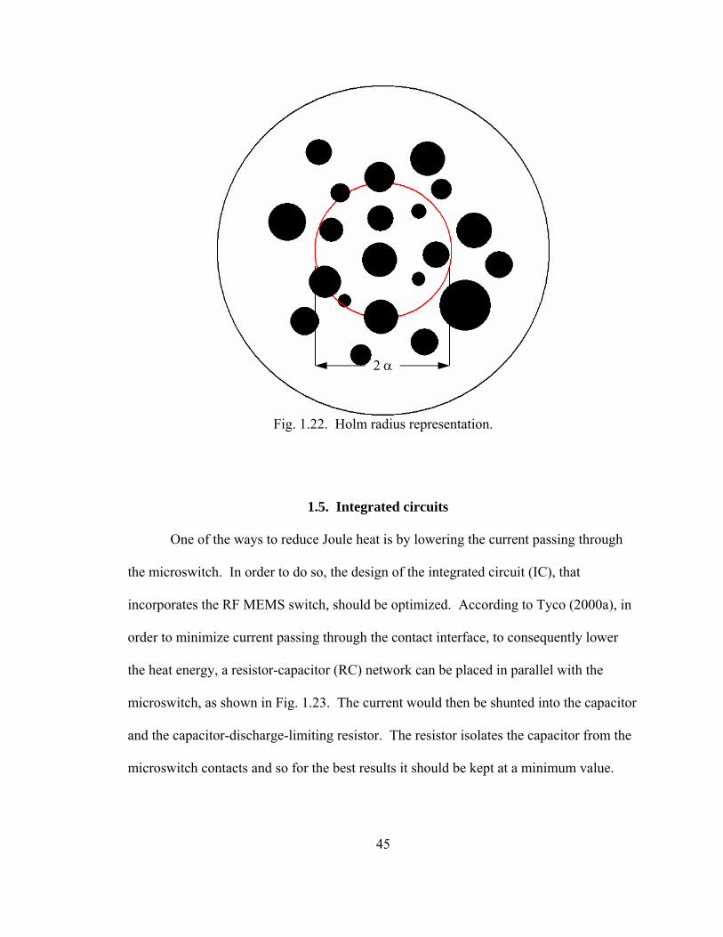
Reid and Starman (2003) show that Holm radius can be used as means of
determining the actual area of a contact. As the area of contact is assumed to be within
the Holm radius, Fig. 1.22, the contact resistance, RC, can be written as
R d
ζ
44
,21
21
⎟⎠⎞
⎜⎝⎛ +=
αρ
naR eC (1.8)
where ρe is the electrical resistivity, a is the average contact asperity radius, n is the
number of asperities per unit area, and α is the Holm radius.
Greenwood and Williamson (1966) model for contacts involved both single and
multiple asperities, however, their studies were based solely on elastic contact modeling.
What this means is that the modeling was considering only small contact loads that were
not large enough to plastically deform the asperities in contact. The modeling was based
on the Hertz theory for elastic deformation (Greenwood and Williamson, 1966),
originally developed for contact interfaces in meshed gears. The equation developed for
calculating the interface contact resistance as proposed by Greenwood and Williamson
(1966) is
,32
34
12 ⎟⎟⎠
⎞⎜⎜⎝
⎛+=
ceC ndna
R πρ (1.9)
where dc is the average center to center distance between contacting asperities.
Another equation proposed for calculating the contact resistance at the interface is
given by Mroczkowski (1998) as
,Dna
R eeC
ρρ+= (1.10)
where D is the diameter of the area over which the contacts are distributed, while other
parameters are as defined previously.
45
Fig. 1.22. Holm radius representation.
1.5. Integrated circuits
One of the ways to reduce Joule heat is by lowering the current passing through
the microswitch. In order to do so, the design of the integrated circuit (IC), that
incorporates the RF MEMS switch, should be optimized. According to Tyco (2000a), in
order to minimize current passing through the contact interface, to consequently lower
the heat energy, a resistor-capacitor (RC) network can be placed in parallel with the
microswitch, as shown in Fig. 1.23. The current would then be shunted into the capacitor
and the capacitor-discharge-limiting resistor. The resistor isolates the capacitor from the
microswitch contacts and so for the best results it should be kept at a minimum value.
2 α

46
In order to prevent the microswitch from receiving the counter-voltage, diodes
can be put into the system. The diode does not let any current back into the microswitch.
It does, however, increase hold-up time of the inductive load. An additional resistor can
be placed in series with the diode to reduce the hold-up time. Nonetheless, the resistor
does reduce the effectiveness of the diode.
Fig. 1.23. Sample RC circuit.
Load
E R
C
47
2. RF MEMS SWITCH CONSIDERED
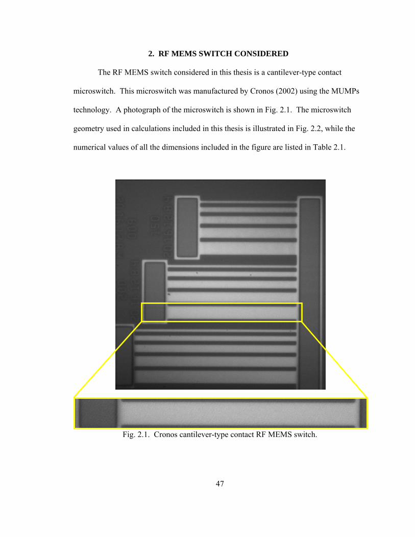
The RF MEMS switch considered in this thesis is a cantilever-type contact
microswitch. This microswitch was manufactured by Cronos (2002) using the MUMPs
technology. A photograph of the microswitch is shown in Fig. 2.1. The microswitch
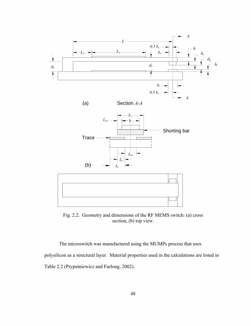
geometry used in calculations included in this thesis is illustrated in Fig. 2.2, while the
numerical values of all the dimensions included in the figure are listed in Table 2.1.
Fig. 2.1. Cronos cantilever-type contact RF MEMS switch.
48
Fig. 2.2. Geometry and dimensions of the RF MEMS switch: (a) cross
section, (b) top view.
The microswitch was manufactured using the MUMPs process that uses
polysilicon as a structural layer. Material properties used in the calculations are listed in
Table 2.2 (Pryputniewicz and Furlong, 2002).
L
Lo Le
Ls Lso
Lc
do
dg
hs
de
bs
0.5 bs
A
ht
h
A
0.5 bt
bt
Shorting bar
Trace
Section A-A
b
(a)
(b)
Lto
Lt
49
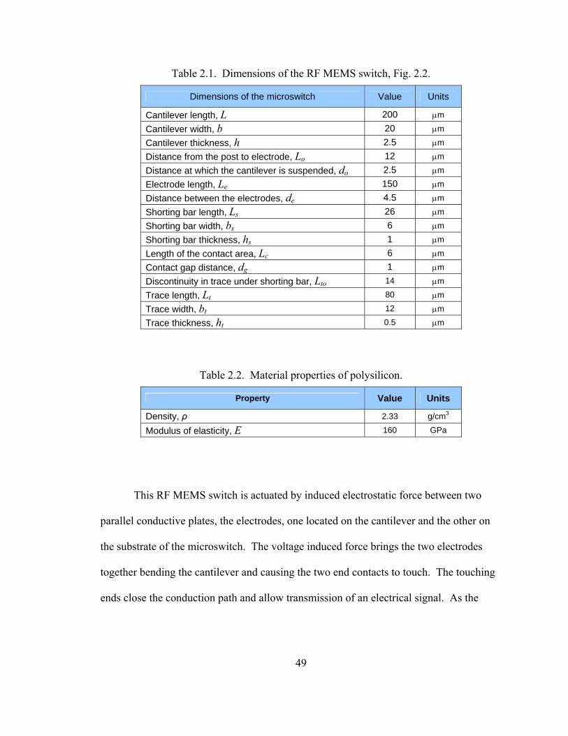
Table 2.1. Dimensions of the RF MEMS switch, Fig. 2.2.
Dimensions of the microswitch Value Units
Cantilever length, L 200 µm
Cantilever width, b 20 µm
Cantilever thickness, h 2.5 µm
Distance from the post to electrode, Lo 12 µm
Distance at which the cantilever is suspended, do 2.5 µm
Electrode length, Le 150 µm
Distance between the electrodes, de 4.5 µm
Shorting bar length, Ls 26 µm
Shorting bar width, bs 6 µm
Shorting bar thickness, hs 1 µm
Length of the contact area, Lc 6 µm
Contact gap distance, dg 1 µm
Discontinuity in trace under shorting bar, Lto 14 µm
Trace length, Lt 80 µm
Trace width, bt 12 µm
Trace thickness, ht 0.5 µm
Table 2.2. Material properties of polysilicon.
Property Value Units
Density, ρ 2.33 g/cm3
Modulus of elasticity, E 160 GPa
This RF MEMS switch is actuated by induced electrostatic force between two
parallel conductive plates, the electrodes, one located on the cantilever and the other on
the substrate of the microswitch. The voltage induced force brings the two electrodes
together bending the cantilever and causing the two end contacts to touch. The touching
ends close the conduction path and allow transmission of an electrical signal. As the

50
voltage between the electrodes is reduced, the elasticity of the cantilever is used to restore
its original, off position.
For the thermal analyses the nominal value of the electrical current used was 300
mA, while the contact resistance was set at 1 Ω, for initial considerations. The current
and contact resistance values are based on MEMS research at Motorola, Inc. Using these
values of current and resistance the total power produced at the contacts of the
microswitch was 0.18 W.
51
3. METHODOLOGY
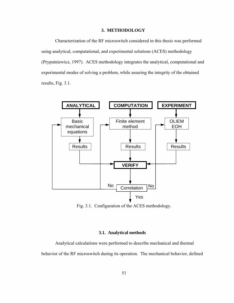
Characterization of the RF microswitch considered in this thesis was performed
using analytical, computational, and experimental solutions (ACES) methodology
(Pryputniewicz, 1997). ACES methodology integrates the analytical, computational and
experimental modes of solving a problem, while assuring the integrity of the obtained
results, Fig. 3.1.
Fig. 3.1. Configuration of the ACES methodology.
3.1. Analytical methods
Analytical calculations were performed to describe mechanical and thermal
behavior of the RF microswitch during its operation. The mechanical behavior, defined
ANALYTICAL COMPUTATION EXPERIMENT
Basic mechanical equations
Finite element method
OLIEM EOH
Results Results Results
VERIFY
Correlation NoNo
Yes

52
in terms of, e.g., stiffness or frequency, was taken into consideration. Thermal
calculations, performed in this thesis, include analyses of Joule heat and dissipation of
this heat.
3.1.1. Mechanical performance
The RF MEMS switch can be analyzed as a one-dimensional model, Fig. 3.2.
The spring in the model represents the spring constant of the cantilever, while the
capacitor denotes the capacitance present between the two electrodes, which may also
represents an electrostatic force present between the electrodes. In order for the model to
be in equilibrium, the summation of forces acting on the cantilever must be equal to zero,
Fig. 3.3, i.e.,
,0=−=↓+ ∑ kES FFF (3.1)
where
2
2
21
e
eeroES
dVbLF εε
= (3.2)
and
.kxFk = (3.3)
In the Eq. 3.2, εo is the dielectric constant of air, εr is the relative permittivity of
the material between electrodes, Le is the length of the electrode, be is the width of the
electrode, V is the voltage drop between the electrodes, and de is the distance between the
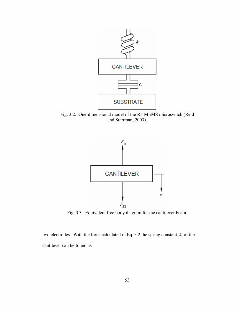
53
Fig. 3.2. One-dimensional model of the RF MEMS microswitch (Reid
and Startman, 2003).
Fig. 3.3. Equivalent free body diagram for the cantilever beam.
two electrodes. With the force calculated in Eq. 3.2 the spring constant, k, of the
cantilever can be found as

54
,21
2
2
eg
eero
dd
VbLk
εε= (3.4)
where dg is the distance between the “open” contacts of the microswitch.
The voltage, V, necessary to actuate the microswitch depends on the area and the
properties of the material used for the electrodes (Reid and Starman, 2003)
eero
ebLεε
FdV
22= (3.5)
where de is the distance between the electrodes. It must be remembered, however, that
due to stress relaxation, with time, the stiffness of the cantilever may chance. The
cantilever spring constant may change as time progresses, thus the electrostatic force,
FES, obtained from Eq. 3.2 may vary with time.
The dynamic mass, m, of the cantilever can be calculated using the following
equation (Pryputniewicz and Furlong, 2002):
,14033 bhLm ρ= (3.6)
where ρ is the density of the cantilever material, b and h are its width and thickness,
respectively, and L is its active length. Using the dynamic mass and the spring constant
of the cantilever, fundamental natural frequency, fo, of the cantilever can be found to be
(Pryputniewicz, 2001; Pryputniewicz and Furlong, 2002; Hsu, 2002)
.21
mkfo π
= (3.7)
Detailed calculations of the parameters from Eqs 3.2 to 3.7 are included in Appendix A.
55
The end contacts are the only electrical conductors that allow signals to pass
through the interface as soon as the microswitch is actuated and the contact gap is closed.
The current passing through the interface is a source of thermal energy, due to Joule heat,
which may be catastrophic to the microswitch. The Joule heat is distributed throughout
the microswitch via heat transfer as described in Section 3.1.2.
3.1.1.1. Cantilever deformations
The microswitch behaves as a cantilever fully constrained at one end. The beam
bends due to the electrostatic force generated between the electrodes. The electrostatic
force acting over the overlap area of the electrodes can be expressed as a concentrated
force in a geometric center of the overlap. This assumption was utilized in all of the
analytical calculations; it was correlated with the results of computational modeling of
the electrostatic force distributed, rather than concentrated, between the electrodes.
The concentrated actuation force is not at the end of the cantilever but is acting in
the middle of the overlap area of the electrodes. Therefore, for the calculation purposes,
the cantilever was divided into two sections: section-1, from the fixed end to the point of
application of the equivalent concentrated electrostatic force, and section-2, from the
point of application of this force to the free end of the cantilever, Fig. 3.4; lengths of
these sections were denoted as L1 and L2, respectively.
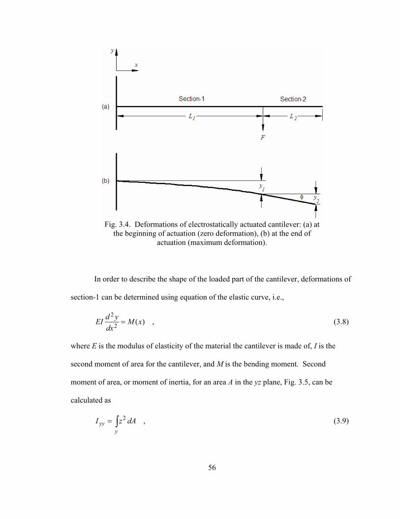
56
Fig. 3.4. Deformations of electrostatically actuated cantilever: (a) at
the beginning of actuation (zero deformation), (b) at the end of actuation (maximum deformation).
In order to describe the shape of the loaded part of the cantilever, deformations of
section-1 can be determined using equation of the elastic curve, i.e.,
,)(2
2xM
dxydEI = (3.8)
where E is the modulus of elasticity of the material the cantilever is made of, I is the
second moment of area for the cantilever, and M is the bending moment. Second
moment of area, or moment of inertia, for an area A in the yz plane, Fig. 3.5, can be
calculated as
,2∫=y
yy dAzI (3.9)
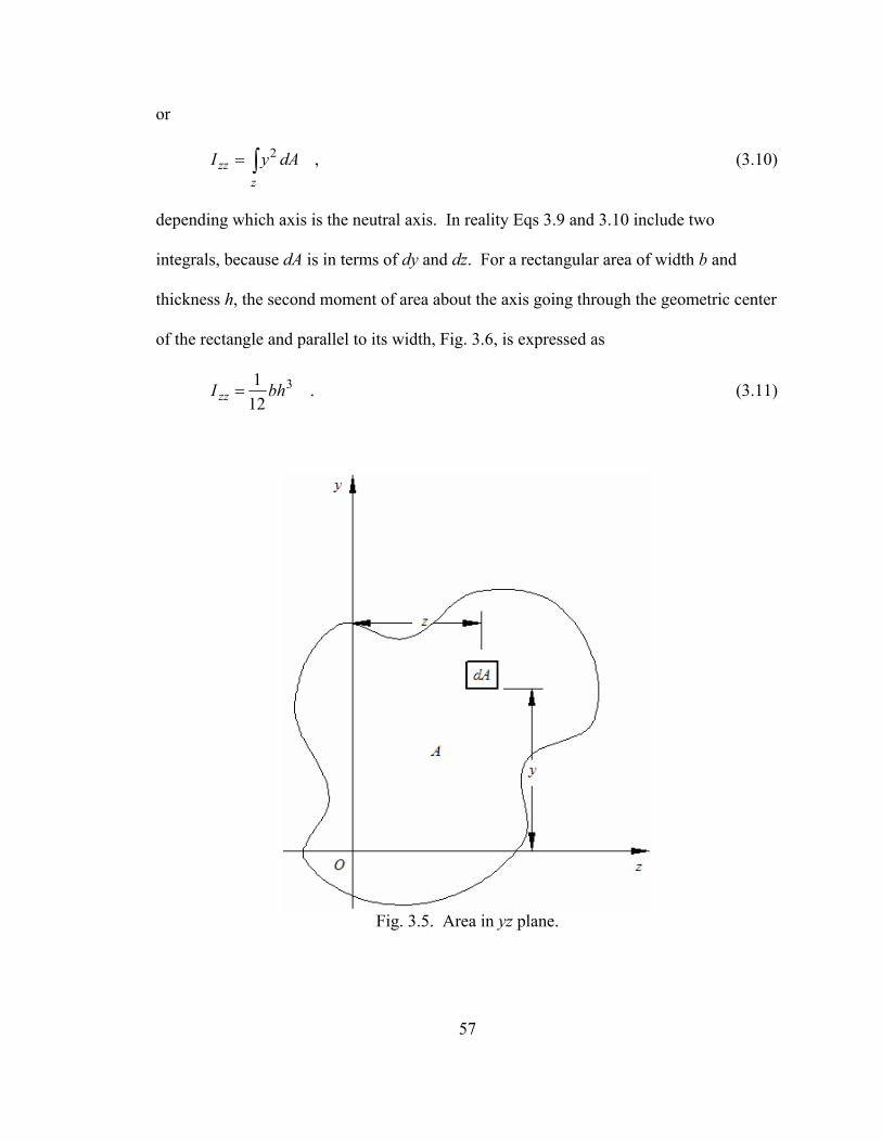
57
or
,2∫=z
zz dAyI (3.10)
depending which axis is the neutral axis. In reality Eqs 3.9 and 3.10 include two
integrals, because dA is in terms of dy and dz. For a rectangular area of width b and
thickness h, the second moment of area about the axis going through the geometric center
of the rectangle and parallel to its width, Fig. 3.6, is expressed as
.121 3bhI zz = (3.11)
Fig. 3.5. Area in yz plane.

58
Fig. 3.6. Cross sectional area indicating axis of bending.
Substituting ( )1)( LxFxM −= into Eq. 3.8 and integrating the elastic curve equation
once produces a slope, or angle, equation
,21
112 CxLx
EIF
dxdy
+⎟⎠⎞
⎜⎝⎛ −= (3.12)
where C1 is a constant of integration that must be solved for by applying known boundary
conditions. Integrating Eq. 3.12 produces a deformation equation
,21
61
212
13 CxCxLx
EIFy ++⎟
⎠⎞
⎜⎝⎛ −= (3.13)
where C2 is the second constant of integration. The constants of integration C1 and C2,
appearing in Eqs 3.12 and 3.13, can be evaluated subject to boundary conditions
characterizing the cantilever, Fig. 3.4, i.e.,
at 00 0 == =xyx (3.14)
and
at .000
===xdx
dyx (3.15)
59
Solution of Eq. 3.12 subject to Eq. 3.15 yields
.01 =C (3.16)
Substituting Eq. 3.16 into Eq. 3.13, and solving the resulting expression subject to Eq.
3.14, we obtain
.02 =C (3.17)
Substitution of Eqs 3.16 and 3.17 into Eqs 3.12 and 3.13 yields the following
relationships for the slope and deformations of section-1 of the cantilever loaded as
shown in Fig. 3.4:
( ) ( )112 2
221 Lxx
EIFxLx
EIFx
dxdy
−=⎟⎠⎞
⎜⎝⎛ −= (3.18)
and
( ) ,362
161)( 1
22
13 Lxx
EIFxLx
EIFxy −=⎟
⎠⎞
⎜⎝⎛ −= (3.19)
respectively. Evaluation of Eqs 3.18 and 3.19 at 1Lx = provides boundary conditions for
determination of slope and deformation of section-2 of the cantilever. Resulting
equations for the slope and deformations of section-2 are
( ) 212
1 LEIFx
dxdy
= (3.20)
and
( ) ( ) .31
21 3
112
1 LEIFLxL
EIFxy −−= (3.21)
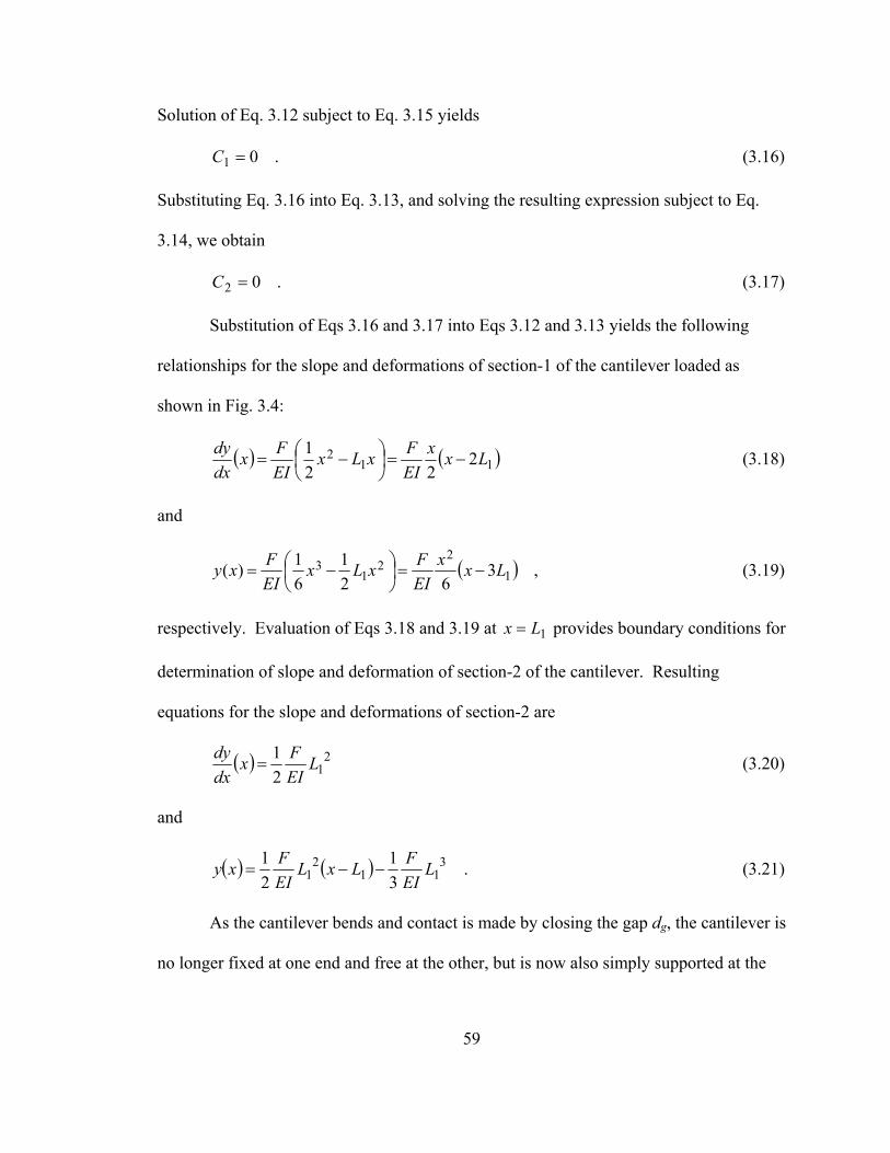
As the cantilever bends and contact is made by closing the gap dg, the cantilever is
no longer fixed at one end and free at the other, but is now also simply supported at the
60
previously free end. This fixed – simply supported system is indeterminate, thus both the
elastic curve equation, and superposition methods need to be used in order to obtain
deformations of the system due to the electrostatic actuation and new boundary
conditions. The elastic curve equation was once again utilized to find deformations of
the cantilever as a function of position along its length. The solution was obtained as the
cantilever was divided to two sections. The boundary conditions were applied according
to Fig. 3.7. At the common point of the two sections, the location of the equivalent
electrostatic force, continuity conditions were applied.
Fig. 3.7. The fixed-simply supported cantilever.
As discussed in Appendix A, the deformation equation for both sections, section-1
denoted by x1 and section-2 denoted by x2, is written as
⎟⎠⎞+−−
+⎜⎝⎛ −−+−=
21
31212
21
32
31
211
21
31
21
65
23
61
61
21
21
611)(
FLLFLxFLLxFL
xRxRxFLFLxFxEI
xy AA , (3.22)
61
where
.51263
31
2
211
⎟⎟⎠
⎞⎜⎜⎝
⎛−+−=
L
L
L
LLL
FRA (3.23)
Equation 3.23, however, does not fully resemble the true boundary conditions of
the operating microswitch. The simply supported end of the cantilever is assumed to be
level with the fixed end. In reality, the cantilever must bend a distance of the gap dg
before it makes a contact. The deformations of the cantilever with these more realistic
boundary conditions can still be described by Eq. 3.22, however, the reaction force RA
changes to
,1065126 633
31
2
211 −×+⎟
⎟⎠
⎞⎜⎜⎝
⎛−+−=
LEI
LL
LL
LLFRA (3.24)
where the last term is a result of changed boundary conditions. The force RA represents
the reaction force at the simply supported end of the cantilever at y = 1 µm; for the case
of initial contact ideally RA equals to zero; however, when F increases above nominal
contact force RA achieves nontrivial values. Details of the derivation of Eq. 3.24 are
included in Appendix A.
At the simply supported end the cantilever may experience slipping. The force
due to slip is a function of the normal force experienced by the end of the cantilever, the
curvature of the tip of the cantilever, and the coefficient of friction. For the purposes of
illustrating this force no differentiation was made between the static and the kinematic
coefficients of friction.
According to the Coulomb friction law,
62
,nS FF µ= (3.25)
where FS is the slip force, µ is the friction coefficient, and Fn is the normal force. Based
on Eq. 3.25, the slip force is directly proportional to the normal force with a
proportionality constant equal to the coefficient of friction. The coefficient of friction
dependents on the nature of the surface and the materials in contact. In this thesis a range
of coefficients of friction used was from 0.15 to 0.60 (Beer and Johnston, 1996).
Both the reaction force and the slip force have great effect on the wear of the
contact. Their values then have a direct impact on the overall reliability of the
microswitch. Detailed calculations of deformations of the cantilever are included in
Appendix A.
3.1.2. Thermal analysis
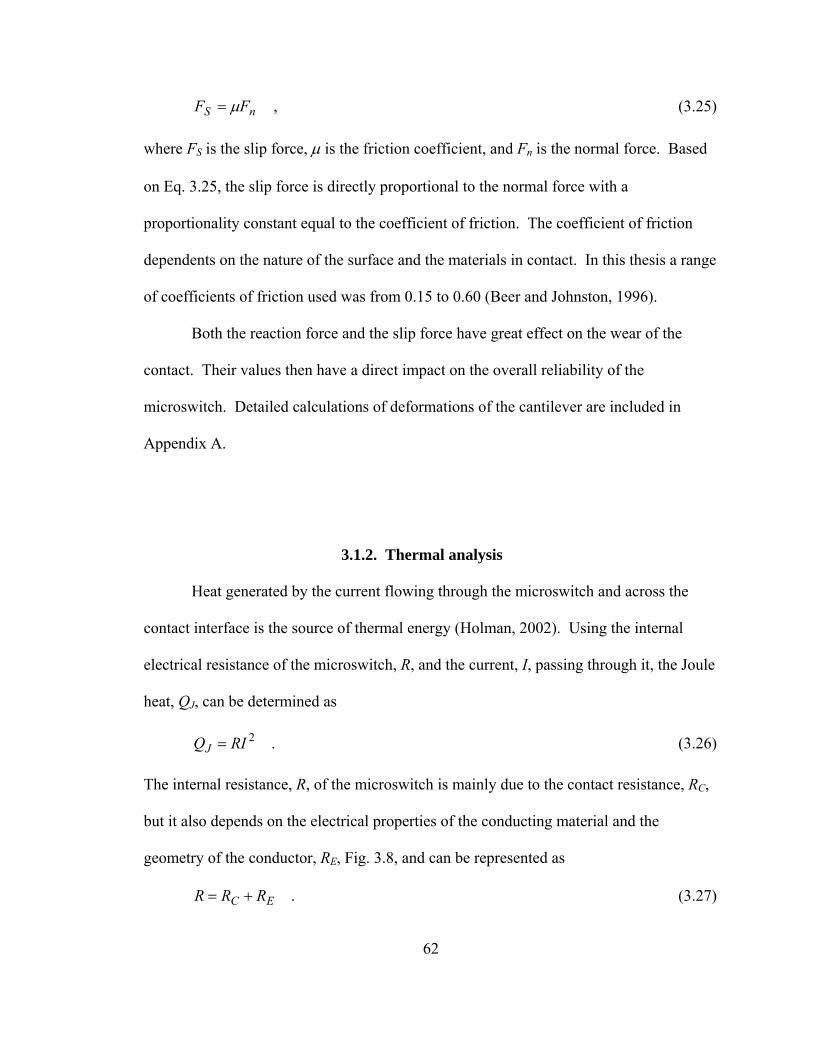
Heat generated by the current flowing through the microswitch and across the
contact interface is the source of thermal energy (Holman, 2002). Using the internal
electrical resistance of the microswitch, R, and the current, I, passing through it, the Joule
heat, QJ, can be determined as
.2RIQJ = (3.26)
The internal resistance, R, of the microswitch is mainly due to the contact resistance, RC,
but it also depends on the electrical properties of the conducting material and the
geometry of the conductor, RE, Fig. 3.8, and can be represented as
.EC RRR += (3.27)
63
The contact resistance depends on the characteristics of the interface. As
discussed in Section 1.4.4 the contact resistance can be calculated using Eqs 1.8 to 1.10.
Perhaps the most appropriate contact resistance equation is (Reid and Starman, 2003)
,4 n
eC FHR πρ= (3.28)
where ρe is the electrical resistivity that is specific to the conducting material, H is the
hardness of that material, and Fn is the normal force.
Fig. 3.8. Current flow through the microswitch contact areas.
The electrical resistance of the conducting material depends on electrical
resistivity of the material out of which the conductor is made, the cross sectional area, A,
of the conductor, and the length of the conductor, L, (Pryputniewicz, 2001), i.e.,
.ALR ee ρ= (3.29)
The Joule heat is dissipated by tree modes of heat transfer (Pryputniewicz, 2001):
convection, Qc, conduction, Qk, and radiation, Qr, i.e.,
TRACE
SHORTING BAR
CANTILEVER
SUBSTRATE
Ri
Re
I I
64
.rkcJ QQQQ ++= (3.30)
The heat due to convection will be transferred away by natural convection, since
no air flow is present in the immediate vicinity of the microswitch. The microswitch
itself will be modeled as a flat horizontal beam. The convected energy can be calculated
as
,)( ∞−= TThAQ scc (3.31)
where Ac is the area through which heat is transferred by convection, Ts is the surface
temperature, T∞ is the ambient temperature, and h is the convective heat transfer
coefficient defined as
,L
kNuh = (3.32)
where k is thermal conductivity of the medium surrounding the microswitch, L is the
length of the cantilever from which the heat is convected away, and Nu is the Nusselt
number calculated using (Holman, 2002)
( ) 31
Pr13.0 LL GrNu = for ,102Pr 8×<LGr (3.33)
or
( ) 31
Pr16.0 LL GrNu = for ,10Pr102 118 <<× LGr (3.34)
In the Eqs 3.33 and 3.34 Pr is the Prandtl number defined as a function of temperature for
specific materials, while Gr is the Grashof number defined by the following equation:
,)(
2
3
νβ LTTg
Gr sL
∞−= (3.35)

65
where g is the gravitational acceleration, β is the volume coefficient of expansion equal to
the reciprocal of the ambient temperature in absolute degrees, but only if the convecting
fluid is assumed to be an ideal gas, and ν is the kinematic viscosity of the convecting
fluid.
Heat transfer by conduction, Qk, for one-dimensional flow, can be determined
using Fourier’s Law
,dxdTkAQ kk −= (3.36)
where k is thermal conductivity of the material, Ak is the area through which conduction
takes place, and dxdT is the temperature gradient in the direction of heat flow.
Equation 3.36 may be written in terms of individual resistances: the thermal resistance of
the conductor and the thermal resistance of the contact. The thermal resistance of the
conductor can be found using
,k
k kAxR = (3.37)
where x is the distance the heat flux travels, k is the thermal conductivity, and Ak is are
cross sectional area through which heat travels by conduction. The thermal contact
resistance is defined as
,1
ccc Ah
R = (3.38)
66
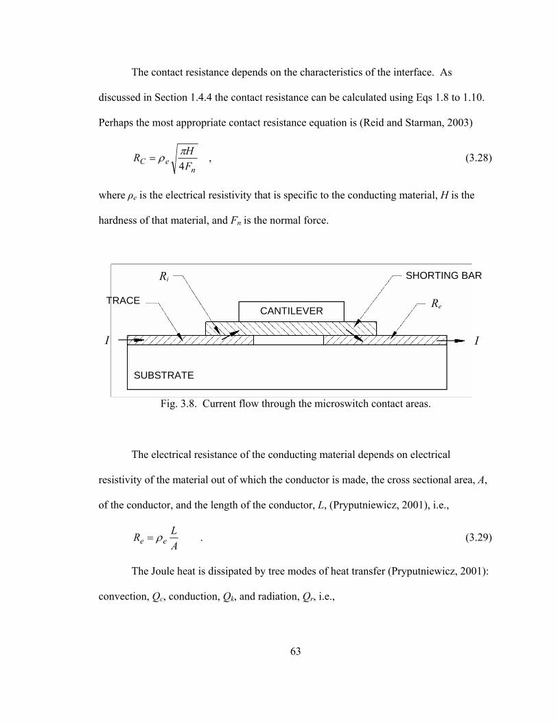
where hc is the contact coefficient, which in general is directly proportional to the surface
roughness and Ac is the contact area, and can be found in Norris, et al. (1979). Therefore,
Eq. 3.36 can be rewritten as
,1
31
⎟⎟⎠
⎞⎜⎜⎝
⎛+⎟⎟
⎠
⎞⎜⎜⎝
⎛+⎟⎟
⎠
⎞⎜⎜⎝
⎛−
=
BB
B
ccAA
Ak
Akx
AhAkx
TTQ (3.39)
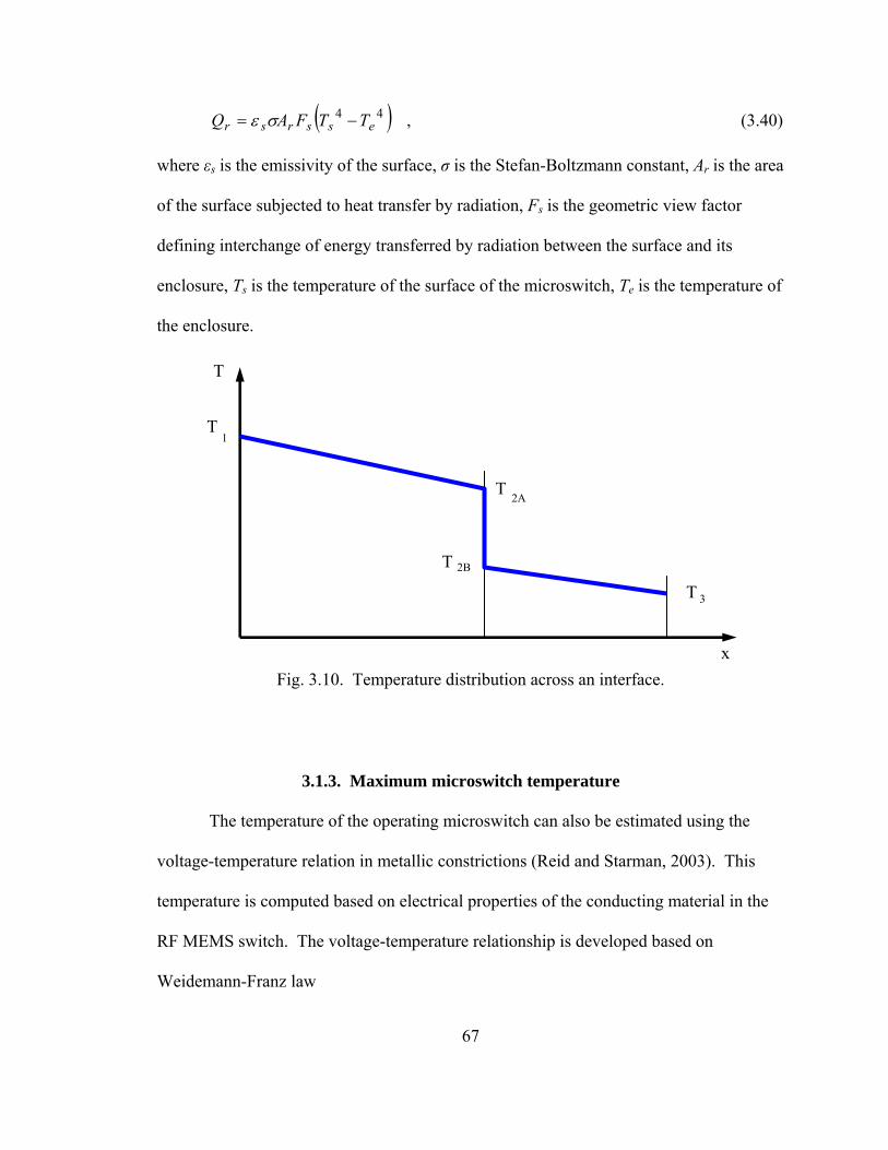
where T1 and T3 are the temperatures at two opposite ends of the microswitch, and other
parameters are as shown in Figs 3.9 and 3.10.
Fig. 3.9. Contact resistance in conduction.
The heat transfer due to radiation for a microswitch that is enclosed by a package
may be written as follows (Pryputniewicz, et al., 2001b, 2001c):
67
( ) ,44essrsr TTFAQ −= σε (3.40)
where εs is the emissivity of the surface, σ is the Stefan-Boltzmann constant, Ar is the area
of the surface subjected to heat transfer by radiation, Fs is the geometric view factor
defining interchange of energy transferred by radiation between the surface and its
enclosure, Ts is the temperature of the surface of the microswitch, Te is the temperature of
the enclosure.
Fig. 3.10. Temperature distribution across an interface.
3.1.3. Maximum microswitch temperature
The temperature of the operating microswitch can also be estimated using the
voltage-temperature relation in metallic constrictions (Reid and Starman, 2003). This
temperature is computed based on electrical properties of the conducting material in the
RF MEMS switch. The voltage-temperature relationship is developed based on
Weidemann-Franz law
T
x
T
T
T
T
1
2A
2B
3
68
,TLk re =ρ (3.41)
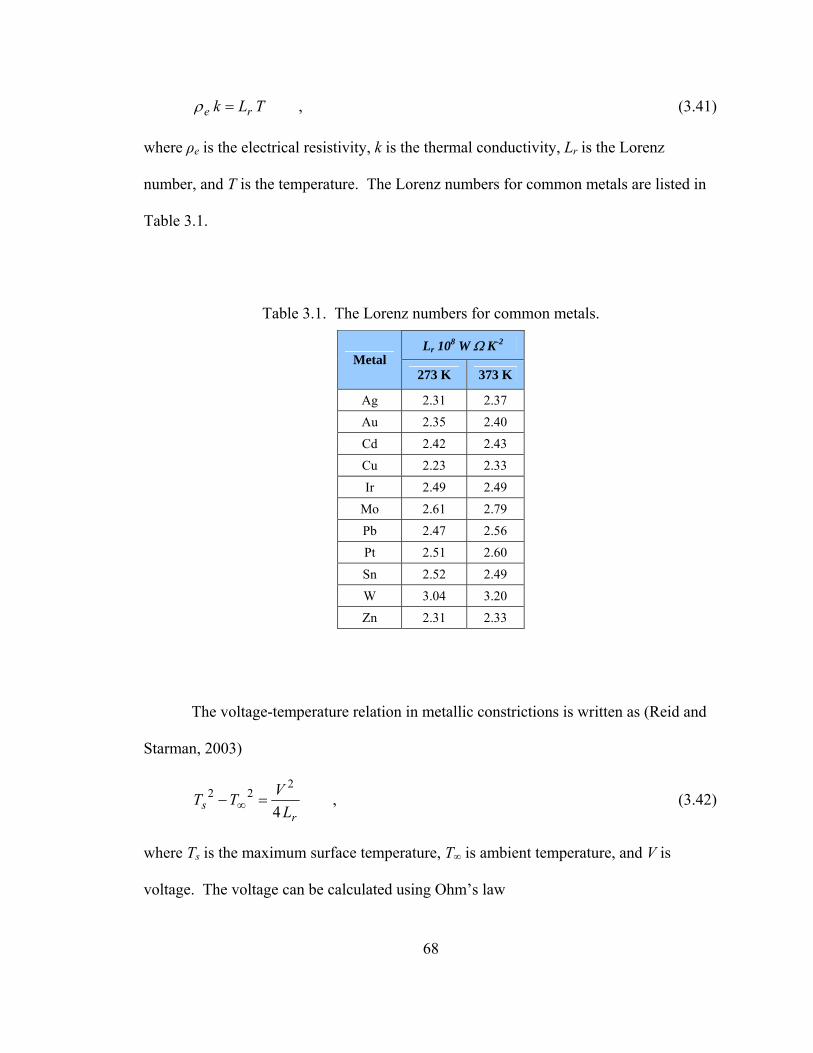
where ρe is the electrical resistivity, k is the thermal conductivity, Lr is the Lorenz
number, and T is the temperature. The Lorenz numbers for common metals are listed in
Table 3.1.
Table 3.1. The Lorenz numbers for common metals.
Lr 108 W Ω K-2 Metal
273 K 373 K
Ag 2.31 2.37 Au 2.35 2.40 Cd 2.42 2.43 Cu 2.23 2.33 Ir 2.49 2.49
Mo 2.61 2.79 Pb 2.47 2.56 Pt 2.51 2.60 Sn 2.52 2.49 W 3.04 3.20 Zn 2.31 2.33
The voltage-temperature relation in metallic constrictions is written as (Reid and
Starman, 2003)
,4
222
rs L
VTT =− ∞ (3.42)
where Ts is the maximum surface temperature, T∞ is ambient temperature, and V is
voltage. The voltage can be calculated using Ohm’s law
69
,IRV = (3.43)
where V denotes the voltage, I denotes the electrical current, and R denotes the electrical
resistance. Since the voltage-temperature relation, given by Eq. 3.42, works for metallic
constrictions, the resistance used there is the individual contact resistance. Complete
calculations and results of the maximum switch temperature can be found in Appendix B.
3.2. Computational methods
Computer software was used to model the mechanical and thermal characteristics
of the RF MEMS switch considered. The software used in the computational part of
ACES methodology was based on a finite element method.
3.2.1. Mechanical analysis
Computer design and analysis program was used to develop a three-dimensional
model of the microswitch that was considered in this thesis. Finally, the mechanical
behavior, characterized by deformations of the cantilever, was analyzed.
3.2.1.1. Pro/ENGINEER model
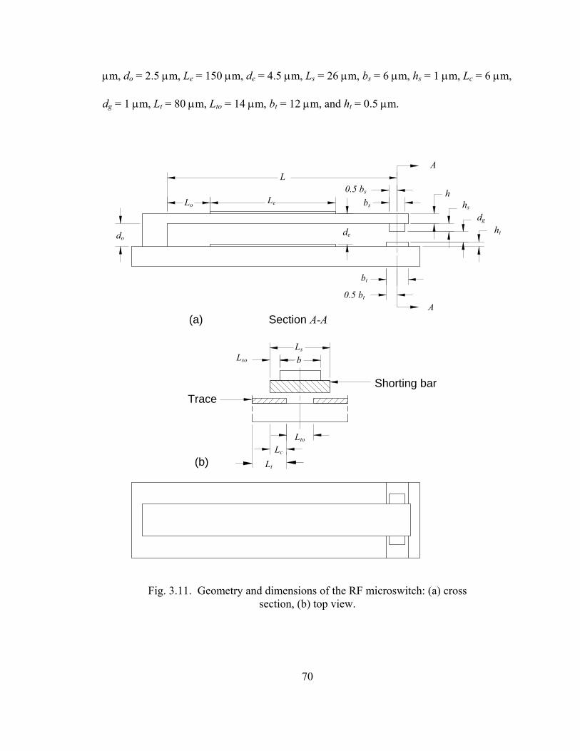
The microswitch modeled was a cantilever-type RF microswitch, Fig. 3.11. The
nominal dimensions used in this study are: L = 200 µm, b = 20 µm, h = 2.5 µm, Lo = 12
70
µm, do = 2.5 µm, Le = 150 µm, de = 4.5 µm, Ls = 26 µm, bs = 6 µm, hs = 1 µm, Lc = 6 µm,
dg = 1 µm, Lt = 80 µm, Lto = 14 µm, bt = 12 µm, and ht = 0.5 µm.
Fig. 3.11. Geometry and dimensions of the RF microswitch: (a) cross section, (b) top view.
L
Lo Le
Ls Lso
Lc
do
dg
hs
de
bs
0.5 bs
A
ht
h
A
0.5 bt
bt
Shorting bar
Trace
Section A-A
b
(a)
(b)
Lto
Lt
71
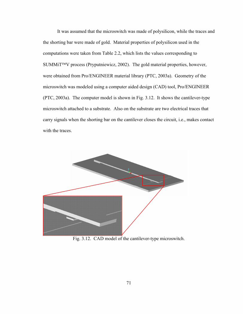
It was assumed that the microswitch was made of polysilicon, while the traces and
the shorting bar were made of gold. Material properties of polysilicon used in the
computations were taken from Table 2.2, which lists the values corresponding to
SUMMiT™V process (Pryputniewicz, 2002). The gold material properties, however,
were obtained from Pro/ENGINEER material library (PTC, 2003a). Geometry of the
microswitch was modeled using a computer aided design (CAD) tool, Pro/ENGINEER
(PTC, 2003a). The computer model is shown in Fig. 3.12. It shows the cantilever-type
microswitch attached to a substrate. Also on the substrate are two electrical traces that
carry signals when the shorting bar on the cantilever closes the circuit, i.e., makes contact
with the traces.
Fig. 3.12. CAD model of the cantilever-type microswitch.
72
3.2.1.2. Pro/MECHANICA algorithms
Pro/MECHANICA (PTC, 2003b) uses the p version of the finite element method
to reduce discrimination error in an analysis. The p version refers to increasing the
degree of the highest complete polynomial (p) within an element, by adding nodes to
elements, degrees of freedom to nodes, or both, but without changing the number of
elements used. This guarantees that a sequence of successively refined meshes will
produce convergence (PTC, 2003c).
The p version represents the displacement within each element using high-order
polynomials, as opposed to the linear and sometimes quadratic or cubic functions. A
single p-element can, therefore, represent more complex state than a conventional finite
element. The use of higher-order elements leads to an increase in the dimensions of the
element matrices, thus requiring larger calculation capabilities. However, fewer higher-
order elements are needed in order to obtain the same degree of accuracy, i.e.,
convergence.
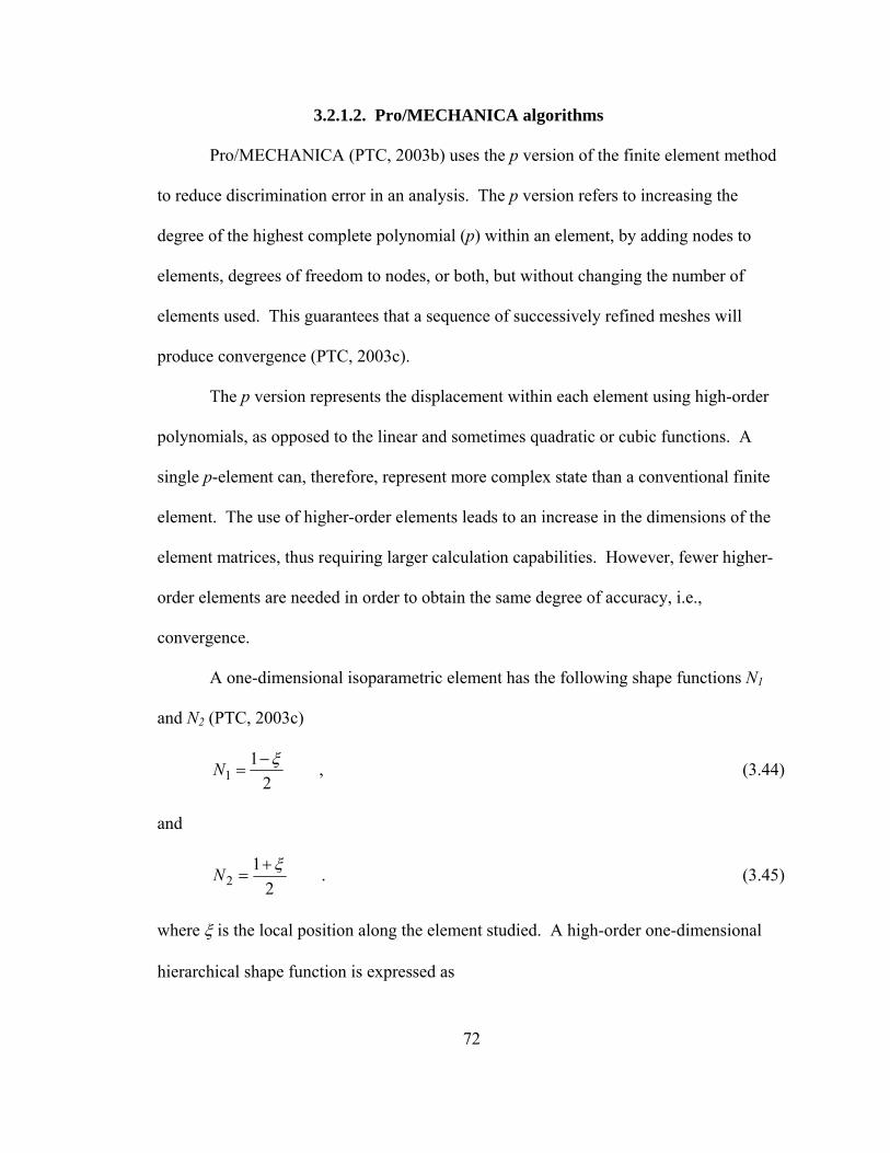
A one-dimensional isoparametric element has the following shape functions N1
and N2 (PTC, 2003c)
,2
11
ξ−=N (3.44)
and
.2
12
ξ+=N (3.45)
where ξ is the local position along the element studied. A high-order one-dimensional
hierarchical shape function is expressed as

73
( ) ,)(1 ξφξ −= iiN (3.46)
for
,1...,,5,4,3 += pi (3.47)
where
( )( )( )
( ) ( ) .)(122
12
21 ξξξφ −−
−= jjj PP
j (3.48)
In Eq. 3.48, the Pj represents the Legendre polynomials, which can be written as
,10 =P (3.49)
,1 ξ=P (3.50)
,)13(21 2
2 −= ξP (3.51)
,)35(21 3
3 ξξ −=P (3.52)
,)33035(81 24
4 +−= ξξP (3.53)
M
( ) .)12(1 11 −+ −+=+ nnn nPPnPn ξ (3.54)
The basis functions N1 and N2 are the nodal shape, or external shape functions, while the
shape functions Ni, i=3, 4, 5, … are the internal shape functions or the internal modes
(Babuska and Szabo, 1991).
74
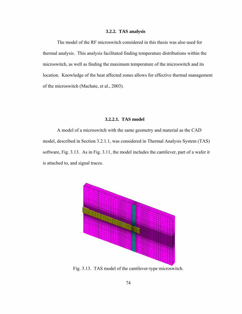
3.2.2. TAS analysis
The model of the RF microswitch considered in this thesis was also used for
thermal analysis. This analysis facilitated finding temperature distributions within the
microswitch, as well as finding the maximum temperature of the microswitch and its
location. Knowledge of the heat affected zones allows for effective thermal management
of the microswitch (Machate, et al., 2003).
3.2.2.1. TAS model
A model of a microswitch with the same geometry and material as the CAD
model, described in Section 3.2.1.1, was considered in Thermal Analysis System (TAS)
software, Fig. 3.13. As in Fig. 3.11, the model includes the cantilever, part of a wafer it
is attached to, and signal traces.
Fig. 3.13. TAS model of the cantilever-type microswitch.

75
3.2.2.2. TAS algorithms
Thermal Analysis System (TAS) is finite difference software that uses resistors in
order to solve for the thermal distributions in a model (Rosato, 2002). In a three-
dimensional model of a single element there might be as many as 28 resistors
(Pryputniewicz, et al., 2002c). These resistors are derived from the equations for the
three modes of heat transfer: convection, conduction and radiation.
The resistance due to convection is calculated according to the equation
,1
cc hA
R = (3.55)
where h is a the convection heat transfer coefficient, Ac is the convective area associated
with each surface node.
The conduction resistance, Rk, is calculated using equation
,k
k kAR ∆
= (3.56)
where ∆ is the distance between the nodes, k is the thermal conductivity, Ak is the cross
sectional area through which conductive heat transfer takes place associated with each
internal node.
Finally, the resistance related to radiation is calculated from each node of the
model to a single reference node according to the equation
( )( ),1
212
22
1 TTTTFAR
srsr ++
=σε
(3.57)
where Ar is the radiation area associated with each surface node, σ is the Stefan-
Boltzmann constant, Fs is the view factor, εs is the emissivity of the surface, and T1 and
76
T2 are the absolute temperatures of the two nodes to which the resistor is attached. As the
TAS model is developed, more than one resistor may be associated with a given pair of
nodes. To speed up the solution process, the multiple resistors can be combined into an
equivalent resistance, providing that individual resistances are temperature and time
independent, according to the equation
.1...111
1
−
++⎟⎟⎠
⎞⎜⎜⎝
⎛+++=
niii RRRR (3.58)
TAS software allows for assigning material properties to as many parts of model
as necessary. It uses these properties, along with the assigned thermal conditions to give
either a steady state or transient solution. The finite difference steady state solution is
computed as (Pryputniewicz, et al., 2002c)
( ) ,1
1
1
1
1
⎟⎟⎠
⎞⎜⎜⎝
⎛∑
+⎟⎟⎠
⎞⎜⎜⎝
⎛∑
+−=
+
+
+
i
ii
i
ii
R
QRT
ddTTprev
(3.59)
where Ti is newly calculated temperature of the i-th node, d is the damping coefficient
with the default value of one, Tiprev is the temperature of the i-th node from previous
iteration, Ti+1 is the temperature of the neighboring node to which resistor Ri+1 is
connected, and Qi is the total heat load on the i-th node. The transient solution is
calculated as
,1
1
previp
ii
i
i TVc
tQRT
T +
∆⎥⎥⎦
⎤
⎢⎢⎣
⎡+⎟⎟
⎠
⎞⎜⎜⎝
⎛∑
=+
+
ρ (3.60)
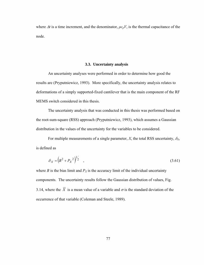
77
where ∆t is a time increment, and the denominator, ρcpV, is the thermal capacitance of the
node.
3.3. Uncertainty analysis
An uncertainty analyses were performed in order to determine how good the
results are (Pryputniewicz, 1993). More specifically, the uncertainty analysis relates to
deformations of a simply supported-fixed cantilever that is the main component of the RF
MEMS switch considered in this thesis.
The uncertainty analysis that was conducted in this thesis was performed based on
the root-sum-square (RSS) approach (Pryputniewicz, 1993), which assumes a Gaussian
distribution in the values of the uncertainty for the variables to be considered.
For multiple measurements of a single parameter, X, the total RSS uncertainty, δX,
is defined as
( ) ,2122
XX PB +=δ (3.61)
where B is the bias limit and PX is the accuracy limit of the individual uncertainty
components. The uncertainty results follow the Gaussian distribution of values, Fig.
3.14, where the X is a mean value of a variable and σ is the standard deviation of the
occurrence of that variable (Coleman and Steele, 1989).
78
Fig. 3.14. Gaussian distribution of the probability values.
For the case of a result that is calculated from many individual variables, a
general uncertainty analysis must be done using, e.g., the RSS approach. This is a
special case of the uncertainty described in Eq. 3.61, where for each variable, Xi,
.0=iXB (3.62)
This reduces Eq. 3.61 to
.ii XX P=δ (3.63)
In order to utilize Eq. 3.63, the general uncertainty analysis must begin by writing a
phenomenological equation for the parameter X for which uncertainty is to be
determined, based on its explicit equation (Pryputniewicz, 1993)
( ) ,,,, 21 nXXXXX K= (3.64)
where X1, X2, …, Xn, are independent parameters defining X. Using Eq. 3.64, the
uncertainty of X is calculated using the RSS approach as
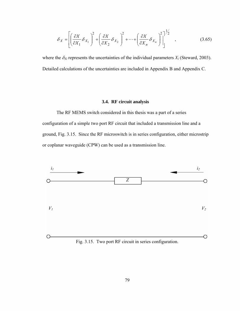
79
,2
122
2
2
121 ⎥
⎥
⎦
⎤
⎢⎢
⎣
⎡⎟⎟⎠
⎞⎜⎜⎝
⎛∂∂
++⎟⎟⎠
⎞⎜⎜⎝
⎛∂∂
+⎟⎟⎠
⎞⎜⎜⎝
⎛∂∂
=nX
nXXX X
XXX
XX δδδδ L (3.65)
where the δXi represents the uncertainties of the individual parameters Xi (Steward, 2003).
Detailed calculations of the uncertainties are included in Appendix B and Appendix C.
3.4. RF circuit analysis
The RF MEMS switch considered in this thesis was a part of a series
configuration of a simple two port RF circuit that included a transmission line and a
ground, Fig. 3.15. Since the RF microswitch is in series configuration, either microstrip
or coplanar waveguide (CPW) can be used as a transmission line.
Fig. 3.15. Two port RF circuit in series configuration.
i1 i2
V1 V2
Z
80
In a microstrip, the ground is located underneath the substrate, and its impedance
is extremely sensitive to the substrate thickness. In general, it was observed that using
microstrip transmission line produced lower losses then the CPW transmission line. The
CPW, however, requires no vias through the substrate in order to ground the microswitch.
For a better understanding of the network an ABCD-matrix can be formed
(Ludwig and Bretchko, 2000). This matrix relates the current and the voltage of the
circuit. An ABCD-matrix of any two port network can be defined as
,2
2
1
1
⎭⎬⎫
⎩⎨⎧
−⎥⎦
⎤⎢⎣
⎡=
⎭⎬⎫
⎩⎨⎧
iV
DCBA
iV
(3.66)
where individual components of the matrix for a series configuration are
,102
1
2
===iV
VA (3.67)
,02
1
2
Zi
VB
V=
−=
=
(3.68)
,002
1
2
===iV
iC (3.69)
.102
1
2
=−
==Vi
iD (3.70)
In Eqs 3.66 to 3.70, V1 and V2 are the voltages in the RF circuit before and after the
microswitch, respectively, i1 and i2 are the currents in the RF circuit before and after the
microswitch, and Z is the impedance of the microswitch, Fig. 3.15.
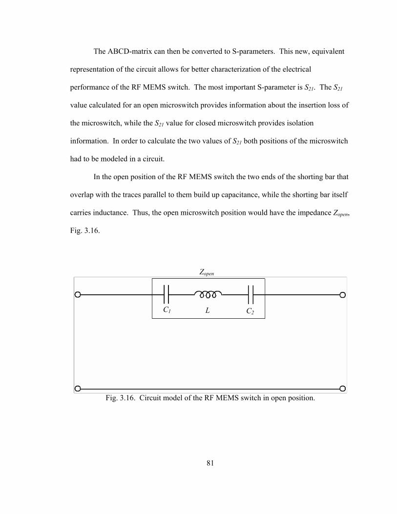
81
The ABCD-matrix can then be converted to S-parameters. This new, equivalent
representation of the circuit allows for better characterization of the electrical
performance of the RF MEMS switch. The most important S-parameter is S21. The S21
value calculated for an open microswitch provides information about the insertion loss of
the microswitch, while the S21 value for closed microswitch provides isolation
information. In order to calculate the two values of S21 both positions of the microswitch
had to be modeled in a circuit.
In the open position of the RF MEMS switch the two ends of the shorting bar that
overlap with the traces parallel to them build up capacitance, while the shorting bar itself
carries inductance. Thus, the open microswitch position would have the impedance Zopen,
Fig. 3.16.
Fig. 3.16. Circuit model of the RF MEMS switch in open position.
LC1 C2
Zopen
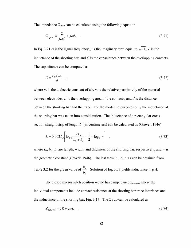
82
The impedance Zopen can be calculated using the following equation
.2 LjCj
Zopen ωω
+= (3.71)
In Eq. 3.71 ω is the signal frequency, j is the imaginary term equal to 1− , L is the
inductance of the shorting bar, and C is the capacitance between the overlapping contacts.
The capacitance can be computed as
,d
AC roεε= (3.72)
where εo is the dielectric constant of air, εr is the relative permittivity of the material
between electrodes, A is the overlapping area of the contacts, and d is the distance
between the shorting bar and the trace. For the modeling purposes only the inductance of
the shorting bar was taken into consideration. The inductance of a rectangular cross
section straight strip of length Ls (in centimeters) can be calculated as (Grover, 1946)
,log212
log002.0 ⎥⎦
⎤⎢⎣
⎡−+
+= w
hbL
LL ess
ses (3.73)
where Ls, bs , hs are length, width, and thickness of the shorting bar, respectively, and w is
the geometric constant (Grover, 1946). The last term in Eq. 3.73 can be obtained from
Table 3.2 for the given value of s
sbh . Solution of Eq. 3.73 yields inductance in µH.
The closed microswitch position would have impedance Zclosed, where the
individual components include contact resistance at the shorting bar trace interfaces and
the inductance of the shorting bar, Fig. 3.17. The Zclosed can be calculated as
,2 LjRZclosed ω+= (3.74)
83
where R is the electrical resistance and other parameters are as previously defined.
Table 3.2. Values of logee for self inductance calculations.
s
sbh
logew s
sbh
logew
0 0 0.50 0.00211 0.025 0.00089 0.55 0.00203 0.05 0.00146 0.60 0.00197 0.10 0.00210 0.65 0.00192 0.15 0.00239 0.70 0.00187 0.20 0.00249 0.75 0.00184 0.25 0.00249 0.80 0.00181 0.30 0.00244 0.85 0.00179 0.35 0.00236 0.90 0.00178 0.40 0.00228 0.95 0.00177 0.45 0.00219 1.00 0.00177
Fig. 3.17. Circuit model of the RF MEMS switch in closed position.
LR1 R2
Zclosed

84
The computed impedance of the open and closed microswitch can then be used
when solving for needed S-parameter. The S21 parameter can be expressed as (Wolff and
Kaul, 1988)
,2
21G
ZVV
S = (3.75)
where VZ and VG are the voltages in the complete circuit that includes the microswitch,
Fig. 3.18. It was assumed that the transmission line had a Zo impedance of 50 Ω on either
side of the microswitch and Z was position dependent. Therefore the S21 parameter is
.2
221 ZZ
ZS
o
o+
= (3.76)
Calculations of the electrical characteristics of the RF circuit are included in Appendix D.
Fig. 3.18. Complete circuit based on RF MEMS switch.
Zo
Zo
VZ
VG
Z
85
3.5. Experimental methods
The samples of RF MEMS switches obtained by Worcester Polytechnic Institute’s
Center for Holographic Studies and Laser micro-mechaTronics (CHSLT) were fabricated
by Cronos (2002). All the samples were not yet operational, because the sacrificial layer
remaining on the substrate, after the Multi-User MEMS Processes (MUMPs) fabrication
(Koester, et al., 2001), has not been removed, i.e., the microswitches were not released.
The samples have also not been wire-bonded to make electrical connections. Therefore,
no experimental analysis was performed on the operation of those microswitches.
However, experimental images were obtained using an optoelectronic laser
interferometric microscope (OELIM) setup (Brown and Pryputniewicz, 1998; Brown,
1999; Pryputniewicz and Furlong, 2002, 2003; Pryputniewicz, et al., 2001d). This setup
includes a Nikon microscope with a monochromatic light source and a high-speed, high-
spatial-resolution digital camera, Fig. 3.19. The magnification of the microscope
objective used to obtain the images was 30X, while its numerical aperture was 0.55.
For future experiments an OELIM system must be used. Basic configuration of
the OELIM system is shown in Fig. 3.20. In this configuration, laser light is launched
into a single mode optical fiber by means of a microscope objective (MO). Then, the
single mode fiber is coupled into two fibers by means of a fiber optic directional coupler
(DC). One of the optical fibers comprising the DC is used to illuminate the object, while
the output from the other fiber provides reference against which the signals from the
object are recorded. Both, the object and reference beams are combined by the
interferometer (IT) and recorded by the system camera (CCD).
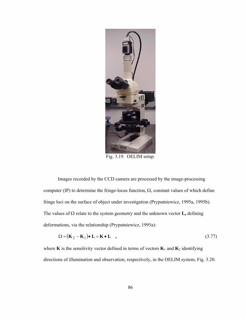
86
Fig. 3.19. OELIM setup.
Images recorded by the CCD camera are processed by the image-processing
computer (IP) to determine the fringe-locus function, Ω, constant values of which define
fringe loci on the surface of object under investigation (Pryputniewicz, 1995a, 1995b).
The values of Ω relate to the system geometry and the unknown vector L, defining
deformations, via the relationship (Pryputniewicz, 1995a):
( ) ,LKLKK •=•−=Ω 12 (3.77)
where K is the sensitivity vector defined in terms of vectors K1 and K2 identifying
directions of illumination and observation, respectively, in the OELIM system, Fig. 3.20.
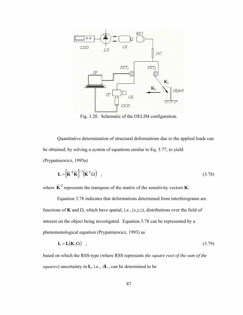
87
Fig. 3.20. Schematic of the OELIM configuration.
Quantitative determination of structural deformations due to the applied loads can
be obtained, by solving a system of equations similar to Eq. 3.77, to yield
(Pryputniewicz, 1995a)
[ ] ( ) ,~~~ T1T Ω=−
KKKL (3.78)
where T~K represents the transpose of the matrix of the sensitivity vectors K.
Equation 3.78 indicates that deformations determined from interferograms are
functions of K and Ω, which have spatial, i.e., (x,y,z), distributions over the field of
interest on the object being investigated. Equation 3.78 can be represented by a
phenomenological equation (Pryputniewicz, 1993) as
( ) ,, Ω= KLL (3.79)
based on which the RSS-type (where RSS represents the square root of the sum of the
squares) uncertainty in L, i.e., Lδ , can be determined to be
88
,2/122
⎥⎥⎦
⎤
⎢⎢⎣
⎡⎟⎠⎞
⎜⎝⎛ Ω
Ω∂∂
+⎟⎠⎞
⎜⎝⎛
∂∂
= δδδ LKKLL (3.80)
where KL ∂∂ / and Ω∂∂ /L represent partial derivatives of L with respect to K and Ω,
respectively, while Kδ and Ωδ represent the uncertainties in K and Ω, respectively. It
should be remembered that K, L, and Ω are functions of spatial coordinates (x,y,z), i.e., K
= K(x,y,z), L = L(x,y,z), and Ω = Ω(x,y,z), respectively, when performing partial
differentiations. After evaluating, Eq. 3.80 indicates that Lδ is proportional to the
product of the local value of L with the RSS value of the ratios of the uncertainties in K
and Ω to their corresponding local values, i.e.,
.2/122
⎥⎥⎦
⎤
⎢⎢⎣
⎡⎟⎠⎞
⎜⎝⎛
ΩΩ
+⎟⎠⎞
⎜⎝⎛∝
δδδKKLL (3.81)
For typical geometries of the OEH systems, based on which the OELIM methodology
was developed, used in recording of interferograms, the values of KK /δ are less than
0.01. However, for small deformations, the typical values of ΩΩ /δ are about one order
of magnitude greater than the values for KK /δ (Pryputniewicz, 1981). Therefore, the
accuracy with which the fringe orders are determined influences the accuracy in the
overall determination of deformations (Pryputniewicz, 1981). To minimize this
influence, a number of algorithms for determination of Ω were developed
(Pryputniewicz, 1990). Some of these algorithms require multiple recordings of each of
the two states, in the case of double-exposure method, of the object being investigated
with introduction of a discrete phase step between the recordings.
89
For example, the intensity patterns of the first and the second exposures, ( )yxIn ,
and ( )yxIn ,' , respectively, in the double-exposure sequence can be represented by the
following equations:
( ) ( ) ( ) ( ) ( )[ ]
( ) ( )[ ] nro
roron
yxyx
yxIyxIyxIyxIyxI
θϕϕ +−
++=
,,cos
,,2,,, 2/1
(3.82)
and
( ) ( ) ( ) ( ) ( )[ ]
( ) ( )[ ] ( ) yxyxyx
yxIyxIyxIyxIyxI
nro
roron
,,,cos
,,2,,, 2/1'
Ω++−
++=
θϕϕ , (3.83)
where oI and rI denote the object and reference beam irradiances, respectively, with
(x,y) denoting spatial coordinates, oϕ denotes random phase of the light reflected from
the object, rϕ denotes the phase of the reference beam, nθ denotes the applied n-th phase
step, and Ω is the fringe-locus function relating to the deformations the object incurred
between the first and the second exposures; Ω is what we need to determine. When Ω is
known, it is used in Eq. 3.78 to find L.
In the case of 5-phase-steps algorithm with ,2and,2/3,,2/,0 ππππθ =n the
distribution of the values of Ω can be determined using
( ) ( ) ( )[ ]( ) ( ) ( ) .
,,,2,,2tan,
513
421
⎭⎬⎫
⎩⎨⎧
−−−
=Ω −
yxIyxIyxIyxIyxIyx (3.84)
Results produced by Eq. 3.84 depend on the capabilities of the illumination,
imaging, and processing subsystems of the OEH system. Developments in laser, fiber
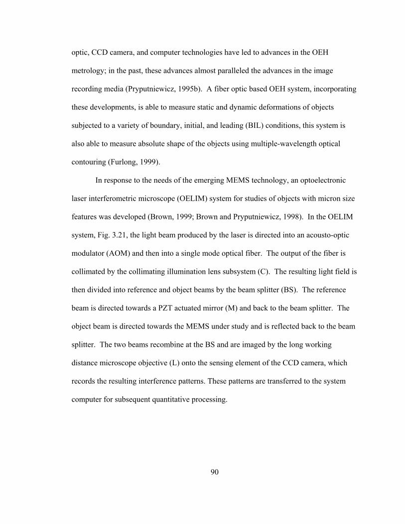
90
optic, CCD camera, and computer technologies have led to advances in the OEH
metrology; in the past, these advances almost paralleled the advances in the image
recording media (Pryputniewicz, 1995b). A fiber optic based OEH system, incorporating
these developments, is able to measure static and dynamic deformations of objects
subjected to a variety of boundary, initial, and leading (BIL) conditions, this system is
also able to measure absolute shape of the objects using multiple-wavelength optical
contouring (Furlong, 1999).
In response to the needs of the emerging MEMS technology, an optoelectronic
laser interferometric microscope (OELIM) system for studies of objects with micron size
features was developed (Brown, 1999; Brown and Pryputniewicz, 1998). In the OELIM
system, Fig. 3.21, the light beam produced by the laser is directed into an acousto-optic
modulator (AOM) and then into a single mode optical fiber. The output of the fiber is
collimated by the collimating illumination lens subsystem (C). The resulting light field is
then divided into reference and object beams by the beam splitter (BS). The reference
beam is directed towards a PZT actuated mirror (M) and back to the beam splitter. The
object beam is directed towards the MEMS under study and is reflected back to the beam
splitter. The two beams recombine at the BS and are imaged by the long working
distance microscope objective (L) onto the sensing element of the CCD camera, which
records the resulting interference patterns. These patterns are transferred to the system
computer for subsequent quantitative processing.
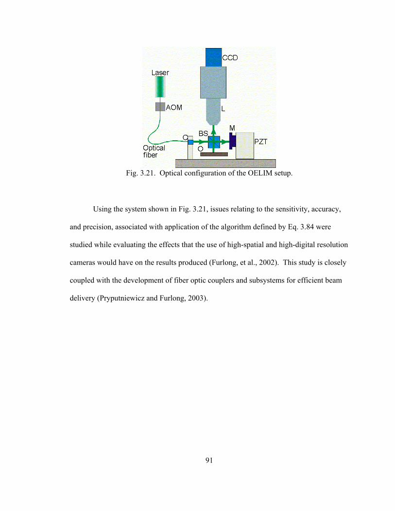
91
Fig. 3.21. Optical configuration of the OELIM setup.
Using the system shown in Fig. 3.21, issues relating to the sensitivity, accuracy,
and precision, associated with application of the algorithm defined by Eq. 3.84 were
studied while evaluating the effects that the use of high-spatial and high-digital resolution
cameras would have on the results produced (Furlong, et al., 2002). This study is closely
coupled with the development of fiber optic couplers and subsystems for efficient beam
delivery (Pryputniewicz and Furlong, 2003).

92
4. RESULTS AND DISCUSSION
The ACES methodology allowed for obtaining well correlated results. Analytical
and computational analyses provided solutions which were in agreement with each other,
leading us to believe that the microswitch characterization was consistent with currently
used practices.
4.1. Analytical results
The RF MEMS contact switch deformations and temperature distributions were
calculated according to the fundamental governing equations. Both mechanical bending
and the heat transfer analyses produced analytical and computational results indicating
deformation and temperature distributions within the RF MEMS switch considered in this
thesis.
4.1.1. Deformations
Based on the principals of structural mechanics, the cantilever deformations due
to the electrostatic force generated between the electrodes were computed. The
magnitude of the electrostatic force required to close the contact gap of 1 µm was 6.44
µN. Deformations of the cantilever at the instant of contact gap closure are shown in Fig.
4.1. The slope for the full length of the cantilever, at the instant of the contact gap
closure, is shown in Fig. 4.2. The force required to close the gap between the contacts is
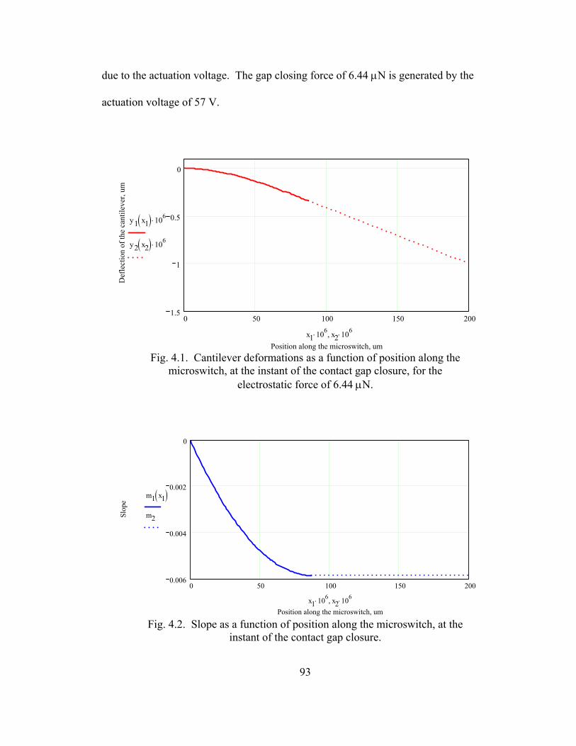
93
due to the actuation voltage. The gap closing force of 6.44 µN is generated by the
actuation voltage of 57 V.
0 50 100 150 2001.5
1
0.5
0
Position along the microswitch, um
Def
lect
ion
of th
e ca
ntile
ver,
um
y1 x1( ) 106⋅
y2 x2( ) 106⋅
x1 106⋅ x2 106⋅,
Fig. 4.1. Cantilever deformations as a function of position along the
microswitch, at the instant of the contact gap closure, for the electrostatic force of 6.44 µN.
0 50 100 150 2000.006
0.004
0.002
0
Position along the microswitch, um
Slop
e
m1 x1( )m2
x1 106⋅ x2 106⋅,
Fig. 4.2. Slope as a function of position along the microswitch, at the
instant of the contact gap closure.
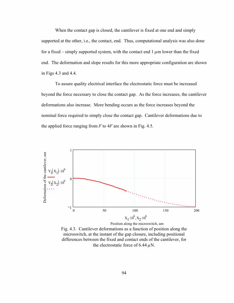
94
When the contact gap is closed, the cantilever is fixed at one end and simply
supported at the other, i.e., the contact, end. Thus, computational analysis was also done
for a fixed – simply supported system, with the contact end 1 µm lower than the fixed
end. The deformation and slope results for this more appropriate configuration are shown
in Figs 4.3 and 4.4.
To assure quality electrical interface the electrostatic force must be increased
beyond the force necessary to close the contact gap. As the force increases, the cantilever
deformations also increase. More bending occurs as the force increases beyond the
nominal force required to simply close the contact gap. Cantilever deformations due to
the applied force ranging from F to 4F are shown in Fig. 4.5.
0 50 100 150 2001
0
1
Position along the microswitch, um
Def
orm
atio
n of
the
cant
ileve
r, um
Y1 X1( ) 106⋅
Y2 X2( ) 106⋅
X1 106⋅ X2 106⋅,
Fig. 4.3. Cantilever deformations as a function of position along the microswitch, at the instant of the gap closure, including positional
differences between the fixed and contact ends of the cantilever, for the electrostatic force of 6.44 µN.
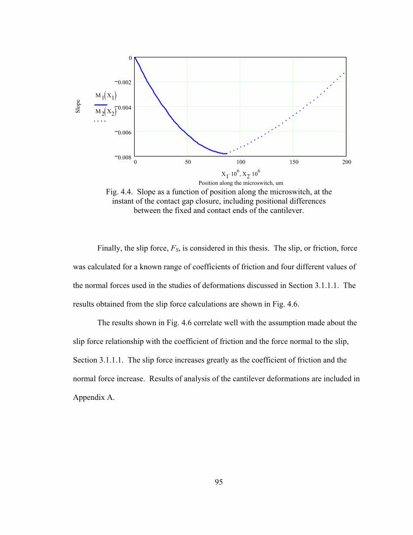
95
0 50 100 150 2000.008
0.006
0.004
0.002
0
Position along the microswitch, um
Slop
e
M1 X1( )M2 X2( )
X1 106⋅ X2 106⋅,
Fig. 4.4. Slope as a function of position along the microswitch, at the
instant of the contact gap closure, including positional differences between the fixed and contact ends of the cantilever.
Finally, the slip force, FS, is considered in this thesis. The slip, or friction, force
was calculated for a known range of coefficients of friction and four different values of
the normal forces used in the studies of deformations discussed in Section 3.1.1.1. The
results obtained from the slip force calculations are shown in Fig. 4.6.
The results shown in Fig. 4.6 correlate well with the assumption made about the
slip force relationship with the coefficient of friction and the force normal to the slip,
Section 3.1.1.1. The slip force increases greatly as the coefficient of friction and the
normal force increase. Results of analysis of the cantilever deformations are included in
Appendix A.
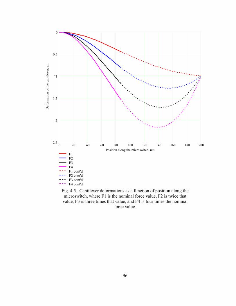
96
0 20 40 60 80 100 120 140 160 180 2002.5
2
1.5
1
0.5
0
F1F2F3F4F1 cont'dF2 cont'dF3 cont'dF4 cont'd
Position along the microswitch, um
Def
orm
atio
n of
the
cant
ileve
r, um
Fig. 4.5. Cantilever deformations as a function of position along the microswitch, where F1 is the nominal force value, F2 is twice that value, F3 is three times that value, and F4 is four times the nominal
force value.
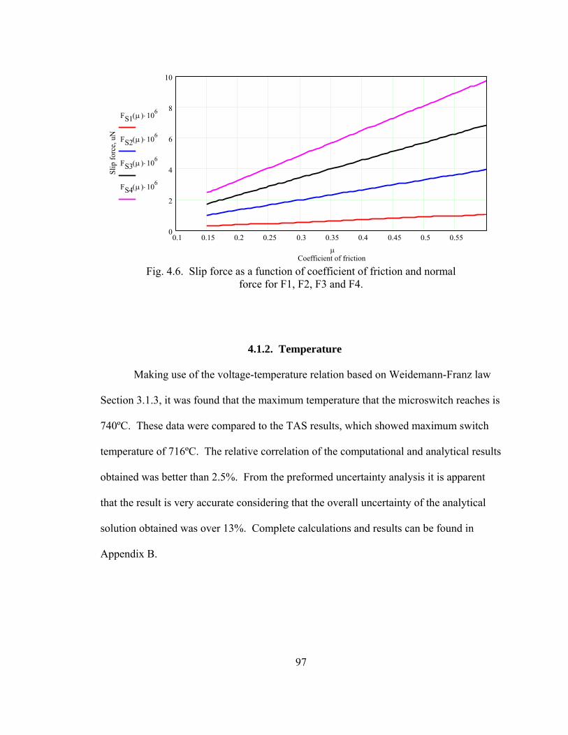
97
0.1 0.15 0.2 0.25 0.3 0.35 0.4 0.45 0.5 0.550
2
4
6
8
10
Coefficient of friction
Slip
forc
e, u
NFS1 µ( ) 106⋅
FS2 µ( ) 106⋅
FS3 µ( ) 106⋅
FS4 µ( ) 106⋅
µ
Fig. 4.6. Slip force as a function of coefficient of friction and normal
force for F1, F2, F3 and F4.
4.1.2. Temperature
Making use of the voltage-temperature relation based on Weidemann-Franz law
Section 3.1.3, it was found that the maximum temperature that the microswitch reaches is
740ºC. These data were compared to the TAS results, which showed maximum switch
temperature of 716ºC. The relative correlation of the computational and analytical results
obtained was better than 2.5%. From the preformed uncertainty analysis it is apparent
that the result is very accurate considering that the overall uncertainty of the analytical
solution obtained was over 13%. Complete calculations and results can be found in
Appendix B.
98
4.2. Computational results
The computational results were obtained using Pro/MECHANICA and TAS
softwares. Pro/MECHANICA software was used as a finite element software in order to
compute the deformations of the RF MEMS switch under the electrostatic loading, while
TAS software was used to find a steady state temperature distributions throughout the
microswitch. Data obtained from the computational models described in Section 3.2
correlated well with the analytical results obtained using algorithms described in Section
3.1.
4.2.1. Deformations
Static deformations were calculated after the CAD microswitch model was
assigned boundary and loading conditions. The distributed electrostatic force in this
analysis was equal in magnitude to the concentrated force used in analytical
considerations. In the Pro/MECHANICA (PTC, 2003b) simulation, the force was evenly
distributed within the overlap area of the electrodes of the microswitch. Figure 4.7
displays the final shape of the cantilever due to the electrostatic load with the maximum
deformation of 1 µm at the contacts. The deformations shown in Fig. 4.7 (in mm scale),
correlate very closely with the analytically obtained deformations.
The Pro/MECHANICA simulation resulted in a maximum beam deformation of
1.02 µm, while the calculations were based on 1 µm gap size. Taking into consideration
the uncertainty in the cantilever deformations, which is about 24% at the simply-
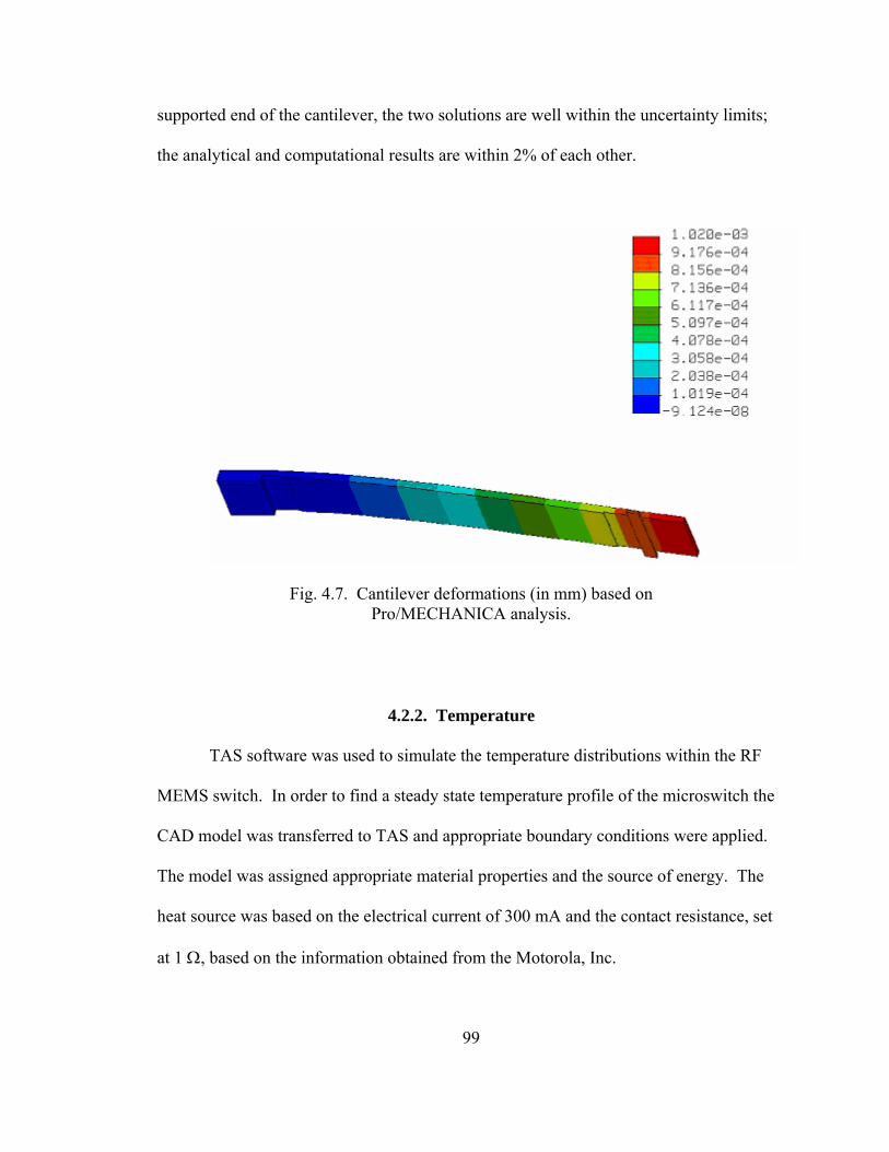
99
supported end of the cantilever, the two solutions are well within the uncertainty limits;
the analytical and computational results are within 2% of each other.
Fig. 4.7. Cantilever deformations (in mm) based on Pro/MECHANICA analysis.
4.2.2. Temperature
TAS software was used to simulate the temperature distributions within the RF
MEMS switch. In order to find a steady state temperature profile of the microswitch the
CAD model was transferred to TAS and appropriate boundary conditions were applied.
The model was assigned appropriate material properties and the source of energy. The
heat source was based on the electrical current of 300 mA and the contact resistance, set
at 1 Ω, based on the information obtained from the Motorola, Inc.
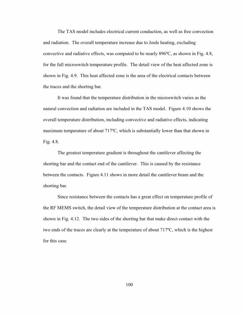
100
The TAS model includes electrical current conduction, as well as free convection
and radiation. The overall temperature increase due to Joule heating, excluding
convective and radiative effects, was computed to be nearly 896ºC, as shown in Fig. 4.8,
for the full microswitch temperature profile. The detail view of the heat affected zone is
shown in Fig. 4.9. This heat affected zone is the area of the electrical contacts between
the traces and the shorting bar.
It was found that the temperature distribution in the microswitch varies as the
natural convection and radiation are included in the TAS model. Figure 4.10 shows the
overall temperature distribution, including convective and radiative effects, indicating
maximum temperature of about 717ºC, which is substantially lower than that shown in
Fig. 4.8.
The greatest temperature gradient is throughout the cantilever affecting the
shorting bar and the contact end of the cantilever. This is caused by the resistance
between the contacts. Figure 4.11 shows in more detail the cantilever beam and the
shorting bar.
Since resistance between the contacts has a great effect on temperature profile of
the RF MEMS switch, the detail view of the temperature distribution at the contact area is
shown in Fig. 4.12. The two sides of the shorting bar that make direct contact with the
two ends of the traces are clearly at the temperature of about 717ºC, which is the highest
for this case.
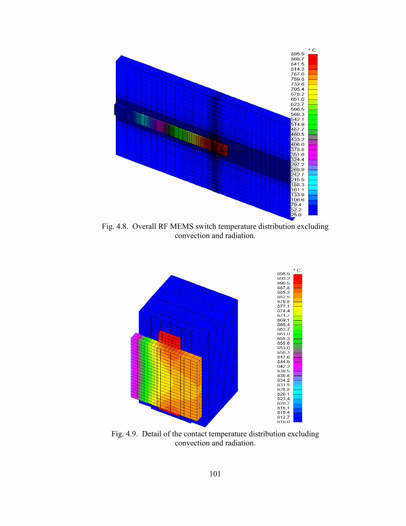
101
Fig. 4.8. Overall RF MEMS switch temperature distribution excluding
convection and radiation.
Fig. 4.9. Detail of the contact temperature distribution excluding
convection and radiation.
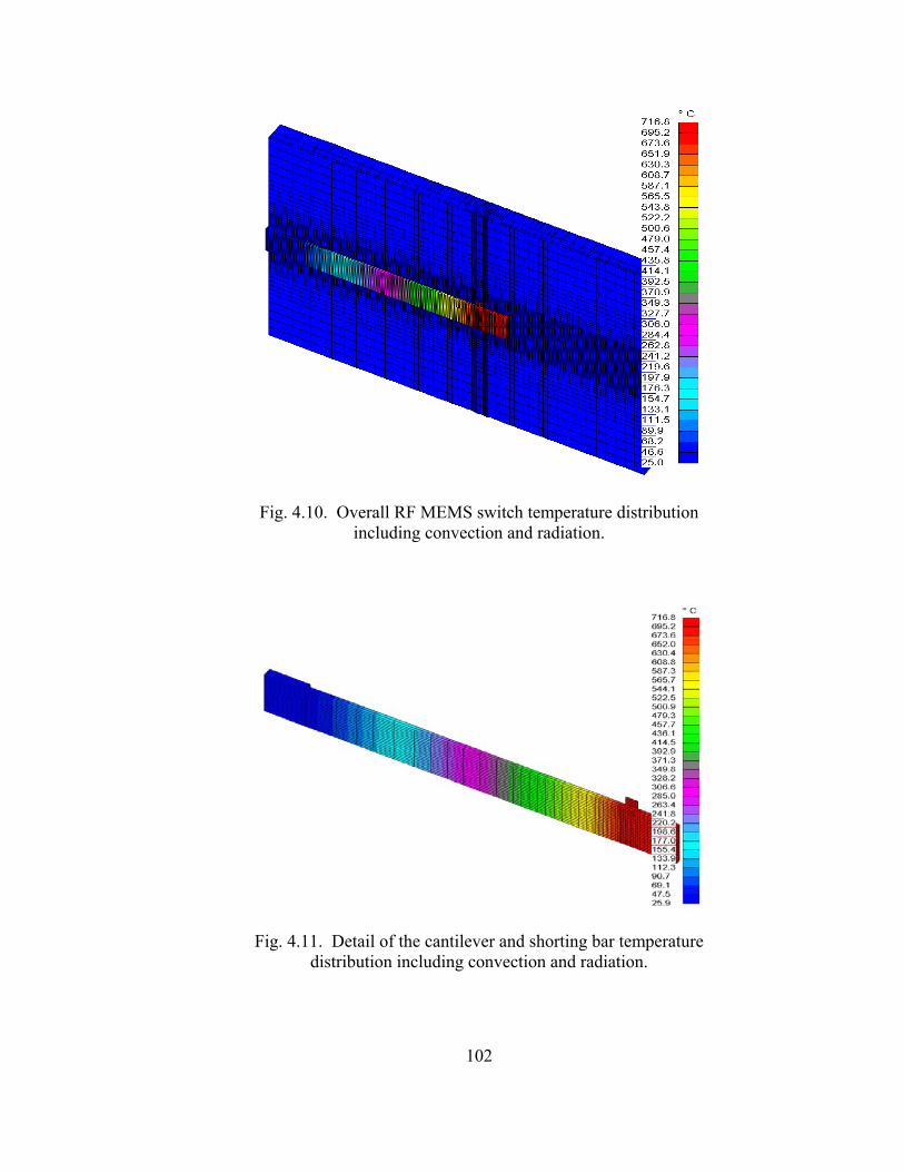
102
Fig. 4.10. Overall RF MEMS switch temperature distribution including convection and radiation.
Fig. 4.11. Detail of the cantilever and shorting bar temperature distribution including convection and radiation.
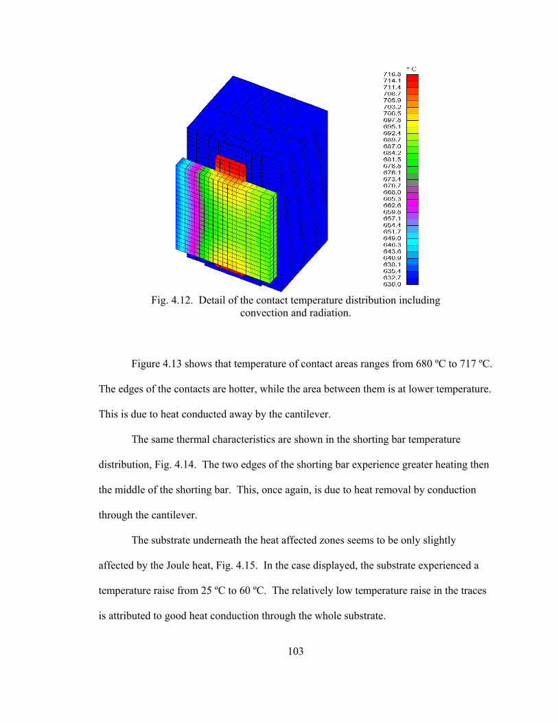
103
Fig. 4.12. Detail of the contact temperature distribution including
convection and radiation.
Figure 4.13 shows that temperature of contact areas ranges from 680 ºC to 717 ºC.
The edges of the contacts are hotter, while the area between them is at lower temperature.
This is due to heat conducted away by the cantilever.
The same thermal characteristics are shown in the shorting bar temperature
distribution, Fig. 4.14. The two edges of the shorting bar experience greater heating then
the middle of the shorting bar. This, once again, is due to heat removal by conduction
through the cantilever.
The substrate underneath the heat affected zones seems to be only slightly
affected by the Joule heat, Fig. 4.15. In the case displayed, the substrate experienced a
temperature raise from 25 ºC to 60 ºC. The relatively low temperature raise in the traces
is attributed to good heat conduction through the whole substrate.
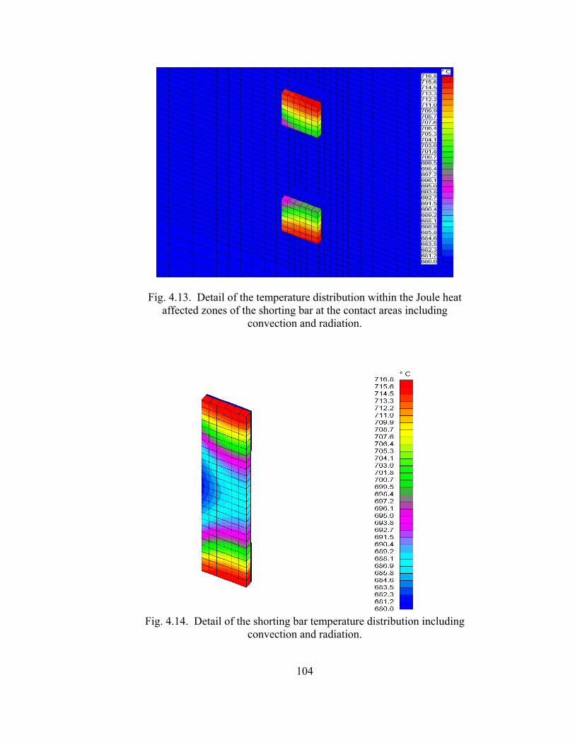
104
Fig. 4.13. Detail of the temperature distribution within the Joule heat affected zones of the shorting bar at the contact areas including
convection and radiation.
Fig. 4.14. Detail of the shorting bar temperature distribution including
convection and radiation.
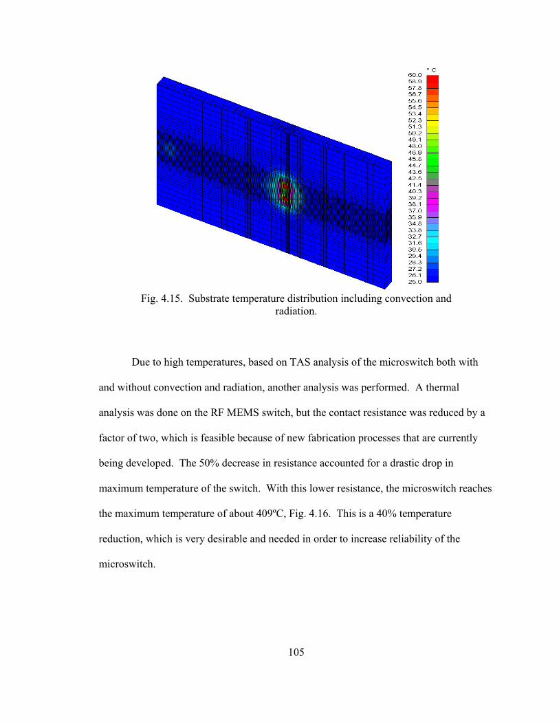
105
Fig. 4.15. Substrate temperature distribution including convection and
radiation.
Due to high temperatures, based on TAS analysis of the microswitch both with
and without convection and radiation, another analysis was performed. A thermal
analysis was done on the RF MEMS switch, but the contact resistance was reduced by a
factor of two, which is feasible because of new fabrication processes that are currently
being developed. The 50% decrease in resistance accounted for a drastic drop in
maximum temperature of the switch. With this lower resistance, the microswitch reaches
the maximum temperature of about 409ºC, Fig. 4.16. This is a 40% temperature
reduction, which is very desirable and needed in order to increase reliability of the
microswitch.
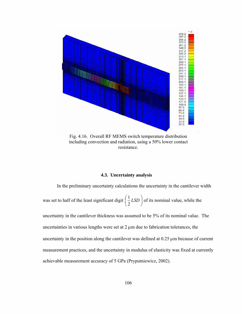
106
Fig. 4.16. Overall RF MEMS switch temperature distribution including convection and radiation, using a 50% lower contact
resistance.
4.3. Uncertainty analysis
In the preliminary uncertainty calculations the uncertainty in the cantilever width
was set to half of the least significant digit ⎟⎠⎞
⎜⎝⎛ LSD
21 of its nominal value, while the
uncertainty in the cantilever thickness was assumed to be 5% of its nominal value. The
uncertainties in various lengths were set at 2 µm due to fabrication tolerances, the
uncertainty in the position along the cantilever was defined at 0.25 µm because of current
measurement practices, and the uncertainty in modulus of elasticity was fixed at currently
achievable measurement accuracy of 5 GPa (Pryputniewicz, 2002).
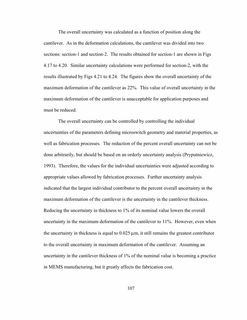
107
The overall uncertainty was calculated as a function of position along the
cantilever. As in the deformation calculations, the cantilever was divided into two
sections: section-1 and section-2. The results obtained for section-1 are shown in Figs
4.17 to 4.20. Similar uncertainty calculations were performed for section-2, with the
results illustrated by Figs 4.21 to 4.24. The figures show the overall uncertainty of the
maximum deformation of the cantilever as 22%. This value of overall uncertainty in the
maximum deformation of the cantilever is unacceptable for application purposes and
must be reduced.
The overall uncertainty can be controlled by controlling the individual
uncertainties of the parameters defining microswitch geometry and material properties, as
well as fabrication processes. The reduction of the percent overall uncertainty can not be
done arbitrarily, but should be based on an orderly uncertainty analysis (Pryputniewicz,
1993). Therefore, the values for the individual uncertainties were adjusted according to
appropriate values allowed by fabrication processes. Further uncertainty analysis
indicated that the largest individual contributor to the percent overall uncertainty in the
maximum deformation of the cantilever is the uncertainty in the cantilever thickness.
Reducing the uncertainty in thickness to 1% of its nominal value lowers the overall
uncertainty in the maximum deformation of the cantilever to 11%. However, even when
the uncertainty in thickness is equal to 0.025 µm, it still remains the greatest contributor
to the overall uncertainty in maximum deformation of the cantilever. Assuming an
uncertainty in the cantilever thickness of 1% of the nominal value is becoming a practice
in MEMS manufacturing, but it greatly affects the fabrication cost.

108
Detailed calculations of the overall uncertainty in the deformations of the
cantilever can be found in Appendix C.
0 20 40 60 80 1000
0.02
0.04
0.06
0.08
Position along the microswitch, um
Ove
rall
unce
rtain
ty, u
m
δY1 X1( ) 106⋅
X1 106⋅
Fig. 4.17. Overall uncertainty in deformations of section-1 of the
cantilever as a function of position along the microswitch.
0 10 20 30 40 50 60 70 80 9010
20
30
40
50
60
Position along the microswitch, um
Perc
ent o
vera
ll un
certa
inty
, %
%δY1 X1( )
X1 106⋅
Fig. 4.18. Percent overall uncertainty in deformations of section-1 of
the cantilever as a function of position along the microswitch.

109
0 20 40 60 80 1000
20
40
60
80
100
Position along the microswitch, um
Perc
ent c
ontri
butio
n, %
%δEY1 X1( )%δIY1 X1( )%δRAY1 X1( )%δX1Y1 X1( )%δL1Y1 X1( )%δLY1 X1( )
X1 106⋅
Fig. 4.19. Percent contributions of uncertainties in individual
parameters to the overall uncertainty in deformations of section-1 of the cantilever as a function of position along the microswitch on a lin-
lin scale.
0 20 40 60 80 1001 .10 5
1 .10 4
1 .10 3
0.01
0.1
1
10
100
Position along the microswitch, um
Perc
ent c
ontri
butio
n, %
%δEY1 X1( )%δIY1 X1( )%δRAY1 X1( )%δX1Y1 X1( )%δL1Y1 X1( )%δLY1 X1( )
X1 106⋅
Fig. 4.20. Percent contributions of uncertainties in individual
parameters to the overall uncertainty in deformations of section-1 of the cantilever as a function of position along the microswitch on a lin-
log scale.
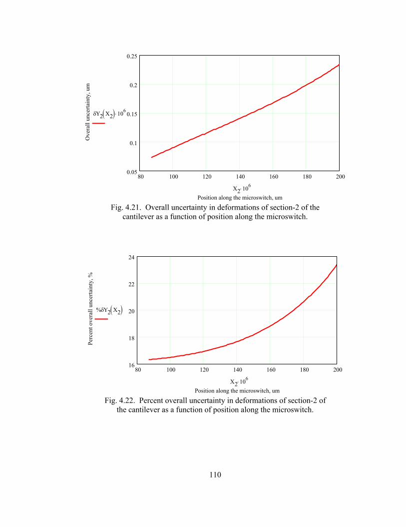
110
80 100 120 140 160 180 2000.05
0.1
0.15
0.2
0.25
Position along the microswitch, um
Ove
rall
unce
rtain
ty, u
m
δY2 X2( ) 106⋅
X2 106⋅
Fig. 4.21. Overall uncertainty in deformations of section-2 of the
cantilever as a function of position along the microswitch.
80 100 120 140 160 180 20016
18
20
22
24
Position along the microswitch, um
Perc
ent o
vera
ll un
certa
inty
, %
%δY2 X2( )
X2 106⋅
Fig. 4.22. Percent overall uncertainty in deformations of section-2 of
the cantilever as a function of position along the microswitch.

111
80 100 120 140 160 180 2000
20
40
60
80
100
Position along the microswitch, um
Perc
ent c
ontri
butio
n, %
%δEY2 X2( )%δIY2 X2( )%δRAY2 X2( )%δX2Y2 X2( )%δL1Y2 X2( )%δLY2 X2( )
X2 106⋅
Fig. 4.23. Percent contributions of uncertainties in individual
parameters to the overall uncertainty in deformations of section-2 of the cantilever as a function of position along the microswitch on a lin-
lin scale.
80 100 120 140 160 180 2001
10
100
Position along the microswitch, um
Perc
ent c
ontri
butio
n, %
%δEY2 X2( )%δIY2 X2( )%δRAY2 X2( )%δL1Y2 X2( )%δLY2 X2( )
X2 106⋅
Fig. 4.24. Percent contributions of uncertainties in individual
parameters to the overall uncertainty in deformations of section-2 of the cantilever as a function of position along the microswitch on a lin-
log scale.
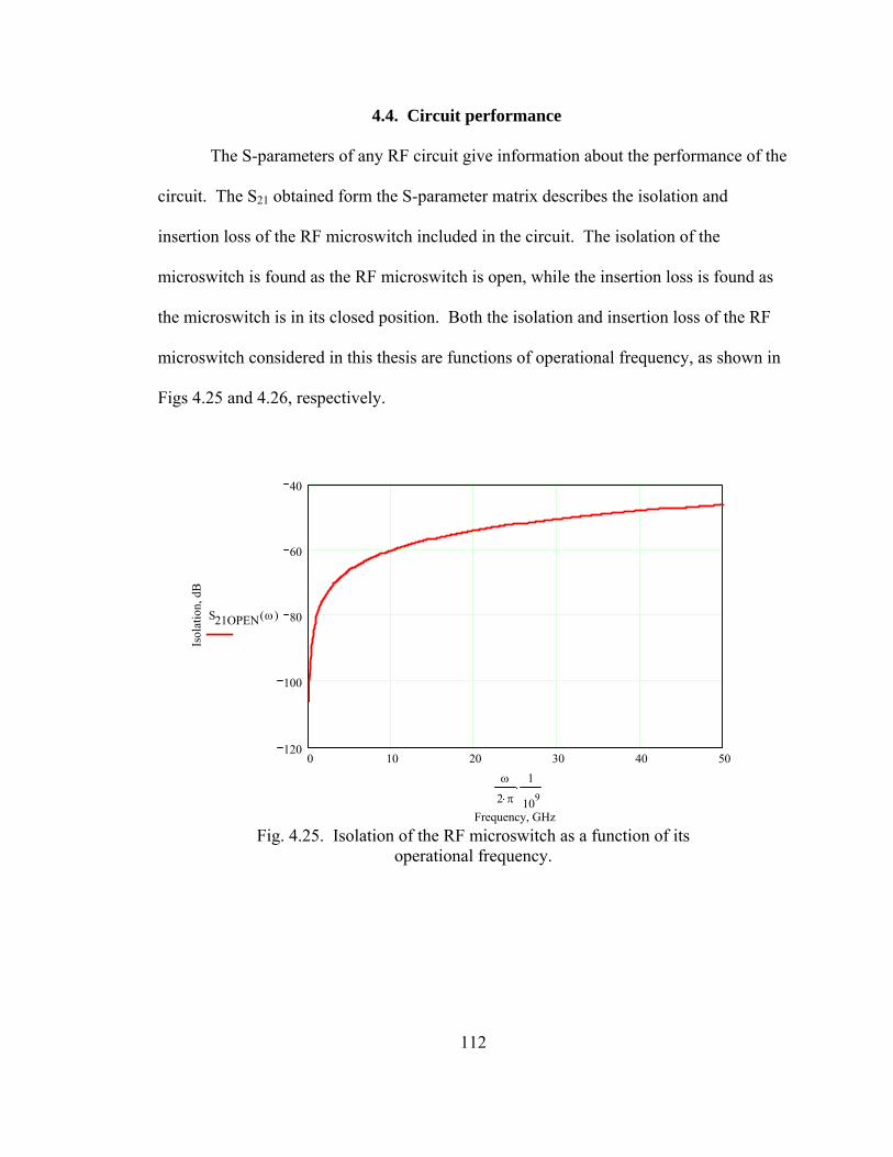
112
4.4. Circuit performance
The S-parameters of any RF circuit give information about the performance of the
circuit. The S21 obtained form the S-parameter matrix describes the isolation and
insertion loss of the RF microswitch included in the circuit. The isolation of the
microswitch is found as the RF microswitch is open, while the insertion loss is found as
the microswitch is in its closed position. Both the isolation and insertion loss of the RF
microswitch considered in this thesis are functions of operational frequency, as shown in
Figs 4.25 and 4.26, respectively.
0 10 20 30 40 50120
100
80
60
40
Frequency, GHz
Isol
atio
n, d
B
S21OPEN ω( )
ω
2 π⋅
1
109⋅
Fig. 4.25. Isolation of the RF microswitch as a function of its
operational frequency.
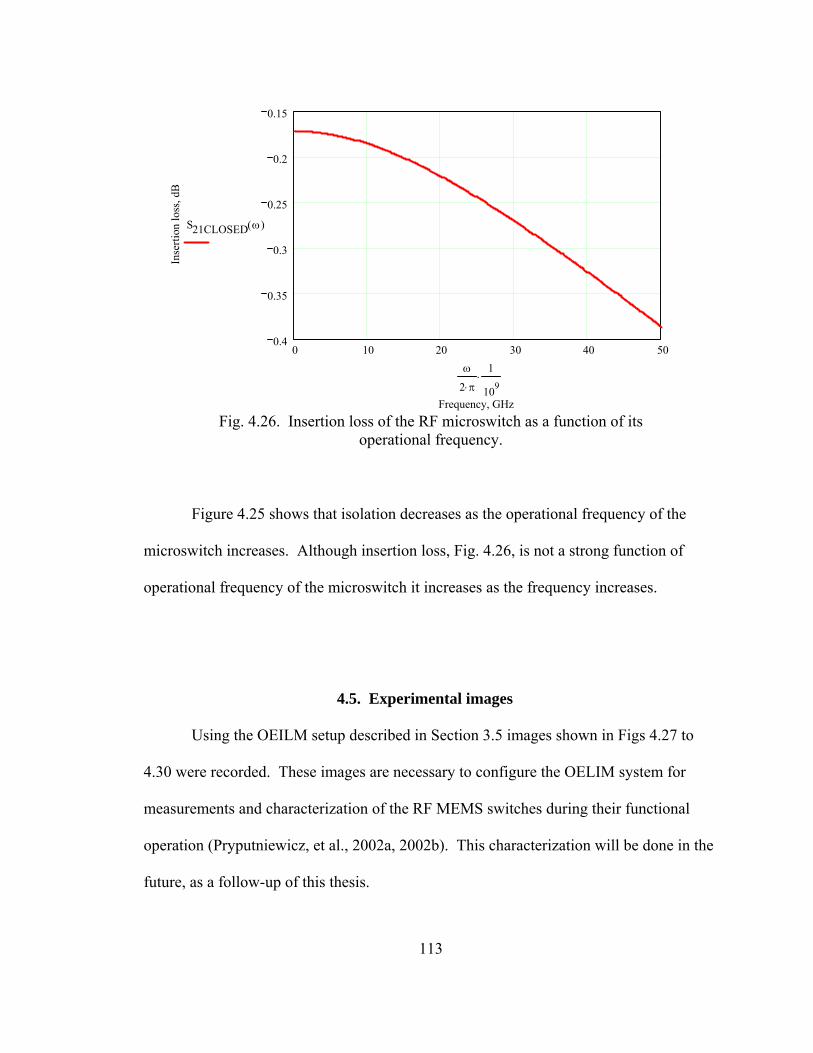
113
0 10 20 30 40 500.4
0.35
0.3
0.25
0.2
0.15
Frequency, GHz
Inse
rtion
loss
, dB
S21CLOSED ω( )
ω
2 π⋅
1
109⋅
Fig. 4.26. Insertion loss of the RF microswitch as a function of its
operational frequency.
Figure 4.25 shows that isolation decreases as the operational frequency of the
microswitch increases. Although insertion loss, Fig. 4.26, is not a strong function of
operational frequency of the microswitch it increases as the frequency increases.
4.5. Experimental images
Using the OEILM setup described in Section 3.5 images shown in Figs 4.27 to
4.30 were recorded. These images are necessary to configure the OELIM system for
measurements and characterization of the RF MEMS switches during their functional
operation (Pryputniewicz, et al., 2002a, 2002b). This characterization will be done in the
future, as a follow-up of this thesis.
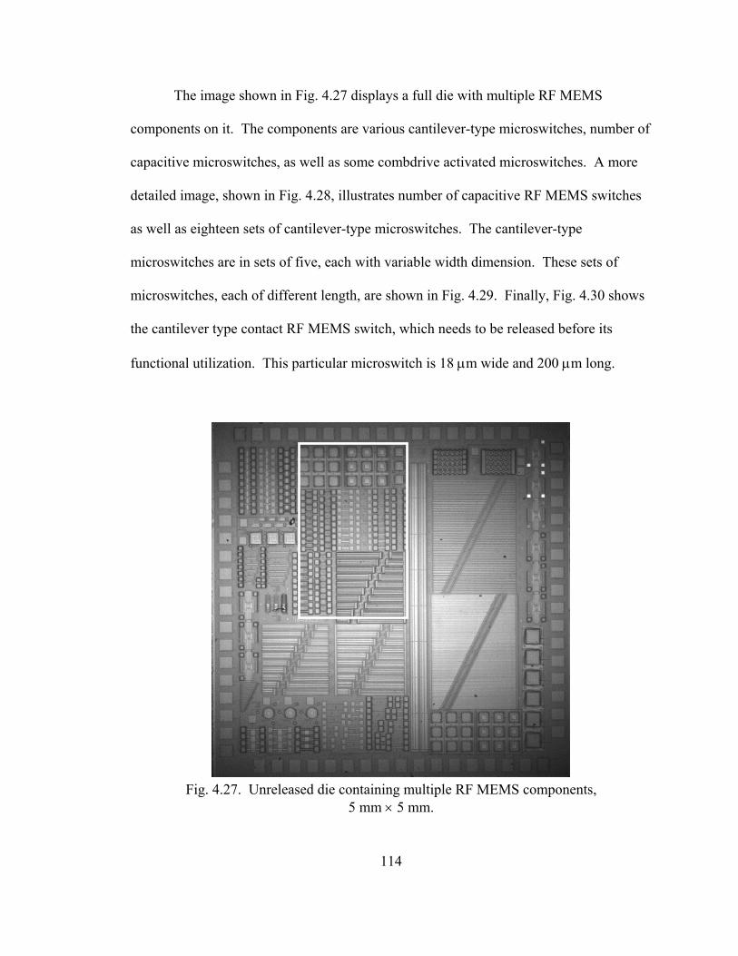
114
The image shown in Fig. 4.27 displays a full die with multiple RF MEMS
components on it. The components are various cantilever-type microswitches, number of
capacitive microswitches, as well as some combdrive activated microswitches. A more
detailed image, shown in Fig. 4.28, illustrates number of capacitive RF MEMS switches
as well as eighteen sets of cantilever-type microswitches. The cantilever-type
microswitches are in sets of five, each with variable width dimension. These sets of
microswitches, each of different length, are shown in Fig. 4.29. Finally, Fig. 4.30 shows
the cantilever type contact RF MEMS switch, which needs to be released before its
functional utilization. This particular microswitch is 18 µm wide and 200 µm long.
Fig. 4.27. Unreleased die containing multiple RF MEMS components,
5 mm × 5 mm.

115
Fig. 4.28. Detail of the unreleased die, highlighted in Fig. 4.27.

116
Fig. 4.29. Unreleased cantilever-type RF MEMS switches of variable
width, highlighted in Fig. 4.28.
Fig. 4.30. Unreleased cantilever type RF MEMS switch, highlighted
in Fig. 4.29, 200 µm long and 18 µm wide.
Interferometric images were obtained using the OELIM methodology. Five phase
shifted images necessary to analyze the deformations of the die, due to residual stresses
developed during the fabrication process, were recorded. Figure 4.31 shows a sample
image of the cantilever-type RF MEMS switches. From these images a wrapped phase
map is obtained, Fig. 4.32. Phase unwrapping is performed in order to determine
deformations of the section of the die being characterized, Fig. 4.33.

117
Fig. 4.31. Sample phase shifted image of the RF MEMS switches.
Fig. 4.32. Wrapped phase map of the RF MEMS switches.
Results shown in Fig. 4.33 indicate a maximum out of plane deformation of 350
nm, which is rather large, considering that the microswitches are not yet released. The
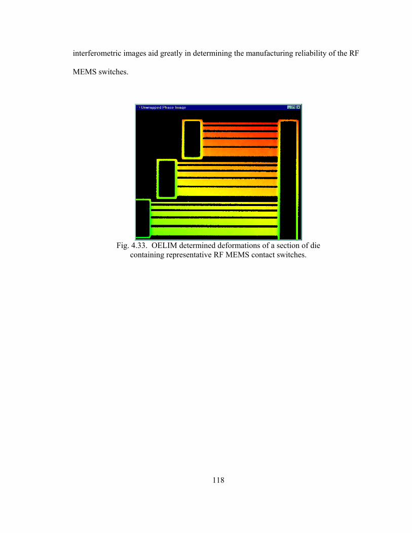
118
interferometric images aid greatly in determining the manufacturing reliability of the RF
MEMS switches.
Fig. 4.33. OELIM determined deformations of a section of die
containing representative RF MEMS contact switches.
119
5. CONCLUSIONS AND FUTURE WORK
Preliminary analytical and computational modeling of the RF MEMS contact
switch were successfully performed using a set of relationships specially developed in
this thesis, Pro/MECHANICA software, and Thermal Analysis System (TAS) softwares.
Preliminary experimental evaluation of a microswitch was also initiated. Use of the
analytical, computational, and experimental approaches to study, in this thesis, reliability
of the RF MEMS switches, is based on the analytical, computational, and experimental
solutions (ACES) methodology.
Results obtained in this thesis indicate correlation between the parameters
specifying operational conditions of the microswitch and the temperatures reached by the
microswitch. The electrostatic force, along with other parameters, like surface finish or
material properties of the conductor, directly affect the electrical resistance of the
contacts. By increasing contact force the electrical resistance can be minimized. Low
electrical resistance has an impact on power dissipation through the switch, thus the
thermal resistance. Controlled thermal resistance directly affects the operational
temperatures and, therefore, reliability of the RF MEMS switches.
Calculations performed according to the equations governing stress distributions
showed that the force of 6.44 µN is sufficient to close the contact gap(s). The
calculations also showed that increasing the force, acting on the cantilever-type
microswitch, increases actual areas of the contacts. The increases in the actual contact
area(s) lead to lower interfacial resistance(s) that, in turn, result in lower temperature
raises due to Joule heating, thus increasing reliability of the RF MEMS switches.
120
Increased force, however, also results in greater wear of the contacts. Greater wear,
eventually, leads to tribological failure of the microswitches, adversely affecting their
reliability. Therefore, careful considerations of multiple effects, frequently conflicting, of
a change in a specific parameter, characterizing functional operation of the RF MEMS
switches, must be made before the change is recommended for implementation.
Computational analyses of deformations of the cantilever-type microswitch
produced results in good agreement with those obtained from the analytical solutions.
The Pro/MECHANICA model showed a deformation of 1.0 µm due to the electrostatic
force of 6.44 µN, thus effectively closing the contact gap, which, for the configuration of
the microswitch used in this thesis, was 1.0 µm.
Computational modeling in TAS clearly showed that two ends of the shorting bar,
in the configuration of the RF MEMS switch considered in this thesis, are affected the
most by the Joule heat. As expected, these heat-affected zones are the contact interfaces
between the shorting bar and the traces. Temperatures of these areas reached the
magnitudes of about 700°C, for the design and operating conditions considered in this
thesis. However, the maximum temperatures reduced to about 400°C when contact
resistance was reduced to half of its original value. At these high temperatures, the
material used for contacts, in this case gold, softens and tends to migrate, causing
material transfer between the contacts, which leads to a premature wear. These are
cumulative temporal effects that should be avoided in order to increase reliability and life
expectancy of the microswitch.
121
In the future, TAS modeling and simulation of thermal effects in the
microswitches should be continued to include different geometries, dimensions,
materials, and operating conditions. Also, experiments should be conducted to measure
actual thermal fields and dynamic characteristics of operational RF MEMS switches.
Measurements of thermal fields are necessary to validate computational results.
This can be achieved by using, e.g., microscope based computer controlled infrared (IR)
camera system, which determines temperature fields based on distributions of emissive
characteristics of the surface, measured during selfcalibration.
Dynamic characteristics are critical for effective optimization of microswitches
because they must close and open on demand and accurate knowledge of their response
times, and corresponding mode shapes, is necessary to assure quality of their functional
operation. These characteristics can be determined using optoelectronic laser
interferometric microscope (OELIM) methodology, which was pioneered at WPI-
ME/CHSLT-NEST laboratories. OELIM methodology provides very high spatial
resolution and nanometer measurement accuracy in full-field-of-view and near real-time
while assuring noninvasive remote measurements and, as such, is particularly suitable for
studies and investigation of MEMS.
Only with the completion of experiments, and correlation of the experimental
results with the analytical and computational results, the ACES methodology will be
fulfilled. This correlation must be judiciously performed subject to rigorous uncertainty
analysis. Then, recommendations can be made to change specific parameters affecting
design and performance of the RF MEMS switches. When these recommendations are

122
implemented and new microswitches are fabricated, they will have to be tested, subject to
the ACES methodology, to determine the effects due to the changes made and to validate
the improvements resulting from these changes.
When validated, the ACES methodology may become an invaluable tool in the
development of reliable RF MEMS switches.

123
REFERENCES
I. Babuska and B. Szabo, 1991, Finite element analysis, Wiley, New York. F. P. Beer and E. R. Johnston, Jr., 1996, Mechanics of materials, 2nd ed., McGraw-Hill, New York. E. Brown, 1998, “RF-MEMS switches for reconfigurable integrated circuits,” IEEE Trans. on Microwave Theory and Techniques, 46:1868-1880. G. C. Brown, 1999, Laser interferometric methodologies for characterizing static and dynamic behavior of MEMS, Ph.D. Dissertation, Worcester Polytechnic Institute, Worcester, MA. G. C. Brown and R. J. Pryputniewicz, 1998, “Holographic microscope for measuring displacements of vibrating microbeams using time-average electro-optic holography,” Opt. Eng., 37:1398-1405. B. Bhushan, 1996, “Contact mechanics of rough surfaces in tribology: single asperity contact,” Appl. Mech. Rev., 49:275-298. B. Bhushan, 1998, “Contact mechanics of rough surfaces in tribology: multiple asperity contact,” Tribology Lett., 4:1-35. W. R. Chang, I. Etsion, and D. B. Bogy, 1987, “An elastic-plastic model for the contact of rough surfaces,” J. Tribology, 109:257-263. H. W. Coleman and W. G. Steele, Jr., 1989, Experimentation and uncertainty analysis for engineers, Wiley, New York, pp. 26-47. Cronos, 2002, MEMS Business Unit, JDS Uniphase, Research Triangle Park, NC. H. J. De Los Santos and R. J. Richards, 2001, “MEMS for RF/microwave wireless applications: the next wave,” Microwave J., 44:20-41. C. Furlong, 1999, Hybrid, experimental and computational, approach for the efficient study and optimization of mechanical and electro-mechanical components, Ph.D. Dissertation, Worcester Polytechnic Institute, Worcester, MA. C. Furlong, J. S. Yokum, and R. J. Pryputniewicz, 2002, “Sensitivity, accuracy, and precision issues in optoelectronic holography based on fiber optics and high-spatial and high-digital resolution cameras,” Proc. SPIE, 4778:216-223.

124
J. A. Greenwood, 1966, “Constriction resistance and the real area of contact,” British J. of Appl. Phys., 17:1621-1632. J. A. Greenwood and J. B. P. Williamson, 1966, “Contact of nominally flat surfaces,” Proc. Roy. Soc. London, A295:300-319. F. W. Grover, 1946, Inductance calculation, working formulas and tables, Dover Publications, New York. J. P. Holman, 2002, Heat transfer, 9th ed., McGraw-Hill, New York. T. R. Hsu, 2002, MEMS & microsystems: design and manufacturing, McGraw-Hill, New York. S. Kalpakjian and S. R. Schmid, 2001, Manufacturing engineering and technology, Prentice-Hall, Upper Saddle River, NJ. D. A. Koester, R. Mahadevan, B. Hardy, and K. W. Markus, 2001, MUMPs® design handbook, Rev. 7.0, Cronos Integrated Microsystems, Research Triangle Park, NC. X. Li, F. Sherman, and C. J. Kim, 1999, “Design and development of MEM microwave switches,” MICRO Project 98-070, University of California, Los Angeles, CA. R. Ludwig and P. Bretchko, 2000, RF circuit design theory and applications, Prentice-Hall, Upper Saddle River, NJ. R. Maboudian, R. Ashurst, and C. Carraro, 2000, “Self-assembled monolayers as anti-stiction coating for MEMS: characteristics and recent developments,” Sensors and Actuators, A82:219-223. M. S. Machate, D. A. Rosato, C. Furlong, and R. J. Pryputniewicz, 2003, “Thermal management of RF MEMS switches: computational investigation,” Proc. 30th Annual Symp. and Exhibition of IMAPS-NE, Boxboro, MA, pp. 174-182. R. S. Mroczkowski, 1998, Electronic connector handbook, McGraw-Hill, New York. R. H. Norris, F. F. Buckland, N. D. Fitzroy, and D. A. Kaminski, 1979, Heat transfer data book, General Electric Company, Corporate Research and Development, Schenectady, NY. K. Petersen, 1979, “Micromechanical switches on silicon.” IBM J. Res. Develop., 23:376-385.
125
D. R. Pryputniewicz, 1997, ACES approach to the development of microcomponents, MS Thesis, Worcester Polytechnic Institute, Worcester, MA. D. R. Pryputniewicz, D. G. Grabbe, and R. J. Pryputniewicz, 2001a, “New microcontact for separable, reusable, high digital speed level-2 interconnections,” Proc. 35th Internat. Symp.on Microelectronics, Denver, CO, pp. 784-798. R. J. Pryputniewicz, 1981, “High precision hologrammetry,“ Internat. Arch. Photogramm., 24:377-386. R. J. Pryputniewicz, 1990, “Automated systems for quantitative analysis of holograms,” Holography, SPIE-IS8:215-246. R. J. Pryputniewicz, 1993, Engineering experimentation, Worcester Polytechnic Institute, Worcester, MA. R. J. Pryputniewicz, 1995a, “Hologram interferometry from silver halide to silicon and… beyond,” Proc. SPIE, 2545:405-427. R. J. Pryputniewicz, 1995b, "Quantitative determination of displacements and strains from holograms," Ch. 3 in Holographic interferometry, Vol. 68 of Springer Series in Sciences, Springer-Verlag, Berlin, pp. 33-72. R. J. Pryputniewicz, 2001, Integrated thermomechanical design and analysis, Worcester Polytechnic Institute, Worcester, MA. R. J. Pryputniewicz, 2002, MEMS SUMMiT™V technology, Worcester Polytechnic Institute, Worcester, MA. R. J. Pryputniewicz and C. Furlong, 2002, MEMS and nanotechnology, Worcester Polytechnic Institute, Worcester, MA. R. J. Pryputniewicz and C. Furlong, 2003, “Novel optoelectronic methodology for testing of MOEMS,” Proc. Internat. Symp. on MOEMS and Miniaturized Systems III, SPIE-4983:11-25. R. J. Pryputniewicz, C. Furlong, S. P. Mizar, P.W. Wilkerson, and A. J. Przekwas, 2001b, “RF MEMS: investigation of a fast contact switch,” Proc. 29th Symp. and Exhibition of IMAPS-NE, Boxboro, MA, pp. 284-288. R. J. Pryputniewicz, P.W. Wilkerson, A. J. Przekwas, and C. Furlong, 2001c, “RF MEMS: modeling and simulation of switch dynamics,” Proc. 35th Internat. Symp.on Microelectronics, Denver, CO, pp. 267-272.
126
R. J. Pryputniewicz, C. Furlong, G. C. Brown, E. J. Pryputniewicz, and M. E. Seta, 2001d, “Optoelectronic method for studies of MEMS,” Proc. Internat. Congress on Experimental and Applied Mechanics for Emerging Technologies, Portland, OR, pp. 817-820. R. J. Pryputniewicz, D. Rosato, and C. Furlong, 2002a, “Measurements and simulation of SMT components,” Proc. 35th Inter. Symp. on Microelectronics, Denver, CO, pp. 151-156. R. J. Pryputniewicz, P. W. Wilkerson, A. J. Przekwas, and C. Furlong, 2002b, “Modeling and simulation of RF MEMS switches,” Paper No. IMECE2002-34504, Am. Soc. Mech. Eng., New York. R. J. Pryputniewicz, C. Furlong, and E. J. Pryputniewicz, 2002c, “Optimization of contact dynamics for an RF MEMS switch,” Paper No. IMECE2002-39504, Am. Soc. Mech. Eng., New York. PTC, 2003a, Pro/ENGINEER user manual, Parametric Technology Corporation, Needham, MA. PTC, 2003b, Pro/MECHANICA user manual, Parametric Technology Corporation, Needham, MA. PTC, 2003c, “Suggested technique for understanding the p-version of the finite element method,” PTC Technical Support Knowledge Base, http://www.ptc.com/cs/cs_24/howto/mst2432/mst2432.htm, Parametric Technology Corporation, Needham, MA. J. R. Reid and L. A. Starman, 2003, “RF MEMS: switches, variable capacitors, and circuits,” IEEE course notes, AFRL/SNHA, Hanscom AFB, MA. D. A. Rosato, 2002, Thermal analysis system – user’s manual, Ver. 6.1, Harvard Thermal, Inc., Harvard, MA. V. Steward, 2003, Modeling of a folded spring supporting MEMS gyroscope, MS Thesis, Worcester Polytechnic Institute, Worcester, MA. Tyco, 2000a, “Relay contact life,” Application Note 13C3236, Tyco Electronics Corporation – P&B, Winston-Salem, NC. Tyco, 2000b, “Contact arc phenomenon,” Application Note 13C3203, Tyco Electronics Corporation – P&B, Winston-Salem, NC.
127
C. Wang, R. Ramadoss, S. Lee, K. C. Gupta, V. Bright, and Y. C. Lee, 2001, “Flexible circuit-based RF MEMS switches,” Paper No. IMECE2001/MEMS-23907, Am. Soc. Mech. Eng., New York. E. A. Wolff and R. Kaul, 1988, Microwave engineering and system applications, Wiley, New York. J. Yao and M. Chang, 1995, “A surface micromachined miniature switches for telecommunications applications with signal frequencies from DC up to 4 GHz,” Transducers’95, 2: 384-387. J. Zou, C. Lui, J. Schutt-Aine, J. Chen, and S. M. Kang, 2000, “Development of a wide tuning range MEMS tunable capacitor for wireless communication systems,” Technical Digest, Internat. Electron Devices Meeting (IEDM), pp. 403-406.

128
APPENDIX A. ANALYSIS OF DEFORMATIONS OF THE CANTILEVER
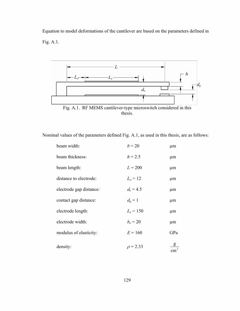
129
Equation to model deformations of the cantilever are based on the parameters defined in
Fig. A.1.
Fig. A.1. RF MEMS cantilever-type microswitch considered in this
thesis.
Nominal values of the parameters defined Fig. A.1, as used in this thesis, are as follows:
beam width: b = 20 µm
beam thickness: h = 2.5 µm
beam length: L = 200 µm
distance to electrode: Lo = 12 µm
electrode gap distance: de = 4.5 µm
contact gap distance: dg = 1 µm
electrode length: Le = 150 µm
electrode width: be = 20 µm
modulus of elasticity: E = 160 GPa
density: ρ = 2.33 3cmg
L
Lo Leh
dgde

130
air dielectric constant: εo = 8.85 10-6 µm
F
relative permittivity of polysilicon: εr = 3 .
The elastic deformation of the cantilever due to the applied force can be determined using
the elastic curve equation
,2
2M(x)
dxydEI =
(A.1)
where
.
121 3hbI = (A.2)
Deformations of the cantilever before contact is made are calculated using parametric
designations shown in Fig. A.2. The parameters L1 and L2 can be rewritten in terms of
the cantilever geometry as
21e
oLLL += (A.3)
and
.12 LLL −= (A.4)
For calculation purposes the ranges of the horizontal or x-distances are defined as
11
1 ...0 LNL,x = (A.5)
and
LN
LLL,Lx ...1112
−+= (A.6)
where N is the number of increments in the set range and it is equal to 100.
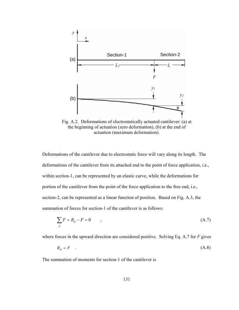
131
Fig. A.2. Deformations of electrostatically actuated cantilever: (a) at
the beginning of actuation (zero deformation), (b) at the end of actuation (maximum deformation).
Deformations of the cantilever due to electrostatic force will vary along its length. The
deformations of the cantilever from its attached end to the point of force application, i.e.,
within section-1, can be represented by an elastic curve, while the deformations for
portion of the cantilever from the point of the force application to the free end, i.e.,
section-2, can be represented as a linear function of position. Based on Fig. A.3, the
summation of forces for section-1 of the cantilever is as follows:
,0=−=∑ FRF oy
(A.7)
where forces in the upward direction are considered positive. Solving Eq. A.7 for F gives
FRo = . (A.8)
The summation of moments for section-1 of the cantilever is
L1
x
L
y
y2
y1
φ
(a)
(b)
Section-1 Section-2
F
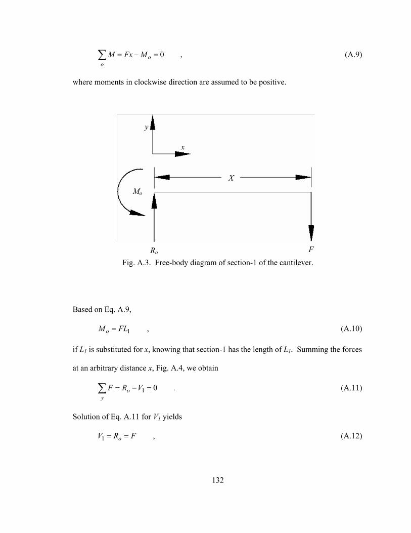
132
,0=−=∑ oo
MFxM (A.9)
where moments in clockwise direction are assumed to be positive.
Fig. A.3. Free-body diagram of section-1 of the cantilever.
Based on Eq. A.9,
,1FLM o = (A.10)
if L1 is substituted for x, knowing that section-1 has the length of L1. Summing the forces
at an arbitrary distance x, Fig. A.4, we obtain
.01 =−=∑ VRF oy
(A.11)
Solution of Eq. A.11 for V1 yields
,1 FRV o == (A.12)
X
x
Mo
y
Ro F
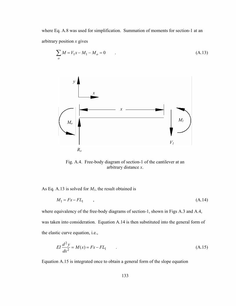
133
where Eq. A.8 was used for simplification. Summation of moments for section-1 at an
arbitrary position x gives
.011 =−−=∑ oo
MMxVM (A.13)
Fig. A.4. Free-body diagram of section-1 of the cantilever at an arbitrary distance x.
As Eq. A.13 is solved for M1, the result obtained is
,11 FLFxM −= (A.14)
where equivalency of the free-body diagrams of section-1, shown in Figs A.3 and A.4,
was taken into consideration. Equation A.14 is then substituted into the general form of
the elastic curve equation, i.e.,
.)( 12
2FLFxxM
dxydEI −== (A.15)
Equation A.15 is integrated once to obtain a general form of the slope equation
x
x
y
Ro V1
M1 Mo
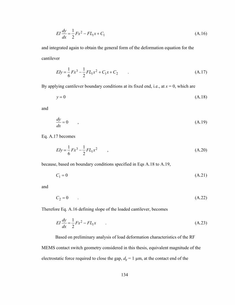
134
112
21 CxFLFx
dxdyEI +−= (A.16)
and integrated again to obtain the general form of the deformation equation for the
cantilever
.
21
61
212
13 CxCxFLFxEIy ++−= (A.17)
By applying cantilever boundary conditions at its fixed end, i.e., at x = 0, which are
0=y (A.18)
and
,0=
dxdy (A.19)
Eq. A.17 becomes
,
21
61 2
13 xFLFxEIy −= (A.20)
because, based on boundary conditions specified in Eqs A.18 to A.19,
01 =C (A.21)
and
.02 =C (A.22)
Therefore Eq. A.16 defining slope of the loaded cantilever, becomes
.
21
12 xFLFx
dxdyEI −= (A.23)
Based on preliminary analysis of load deformation characteristics of the RF
MEMS contact switch geometry considered in this thesis, equivalent magnitude of the
electrostatic force required to close the gap, dg = 1 µm, at the contact end of the

135
cantilever, is 6.44 µN. This nominal value of the equivalent force was used in all
analyses included in this appendix, unless otherwise specified. Therefore, in the
following determinations of deformations and slopes of the cantilever, as function of
position along its length, the concentrated force of 6.44 µN applied in the negative y-
direction at the geometric center of the overlap area of the electrodes actuating the
cantilever, i.e., the force of -6.44 µN, will be used. The equation defining deformations
of section-1 as a function of position along the cantilever can be written, based on Eq.
A.20, as
,
21
61)( 2
113
111 ⎟⎠⎞
⎜⎝⎛ −= xLx
EIFxy (A.24)
while the slope of section-1 as a function of the position along the cantilever, based on
Eq. A.23, is
.
21)( 11
2111 ⎟
⎠⎞
⎜⎝⎛ −= xLx
EIFxm (A.25)
Graphical representations of Eqs A.24 and A.25 are shown in Figs A.5 and A.6,
respectively.
Relationships equivalent to Eqs A.24 and A.25, which define deformations and
slope of section-1 of the cantilever as a function of position along the microswitch, for
section-2 are based on the fact that this section is a straight line characterized by the slope
equal to the slope at the end of section-1, i.e., at x1 = L1, and deformations based on the
slope-intercept representation of a line, where the intercept is defined by the deformation
of section-1 at x1 = L1. That is, deformations of section-2 can be defined as
( ) ( ) ,max112222 yLxmxy +−= (A.26)

136
where x2 is the local coordinate within section-2, m2 is the slope of section-2, and y1max is
the intercept, based on the solution for deformation of section-1 at L1. The specific value
of parameters appearing in Eq. A.26 are determined using Eqs A.24 and A.25. Using Eq.
A.24 evaluated at x1 = L1, we obtain
,313
1max1 L
EIFy = (A.27)
which using the force of -6.44 µN, yields
1103933max1−×−= .y µm . (A.28)
Based on Eq. A.25, evaluated at x1 = L1, the maximum slope of section-1 can be defined
by the equation
2
1max1 21 L
EIFm =
, (A.29)
solution of which, subject to F = -6.44 µN, gives
3
max1 1085045 −×−= .m rad
. (A.30)
Therefore, using the result shown in Eq. A.30, the slope of section-2, as a function of
position along the microswitch, can be shown to be
( ) 3
max122 1085045 −×−== .mxm rad
. (A.31)
Equation A.31 indicates that slope of section-2 is independent of position along the
microswitch. Therefore, substituting Eqs A.28 and A.31 into Eq. A.26, we obtain
( ) ( ) 1
123
22 1039331085045 −− ×−−×−= .Lx.xy µm
. (A.32)
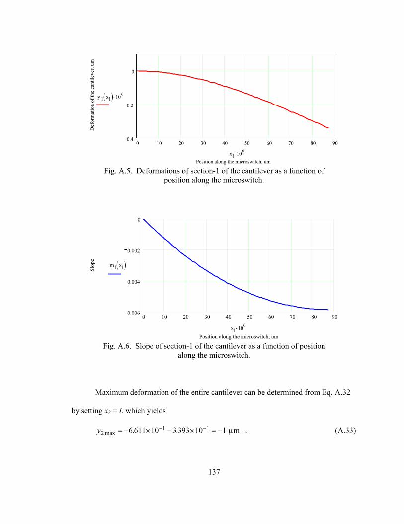
137
0 10 20 30 40 50 60 70 80 900.4
0.2
0
Position along the microswitch, um
Def
orm
atio
n of
the
cant
ileve
r, um
y 1 x1( ) 106⋅
x1 106⋅
Fig. A.5. Deformations of section-1 of the cantilever as a function of
position along the microswitch.
0 10 20 30 40 50 60 70 80 900.006
0.004
0.002
0
Position along the microswitch, um
Slop
e
m1 x1( )
x1 106⋅
Fig. A.6. Slope of section-1 of the cantilever as a function of position
along the microswitch.
Maximum deformation of the entire cantilever can be determined from Eq. A.32
by setting x2 = L which yields
1103933106116 11
max2 −=×−×−= −− ..y µm
. (A.33)
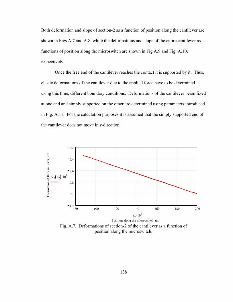
138
Both deformation and slope of section-2 as a function of position along the cantilever are
shown in Figs A.7 and A.8, while the deformations and slope of the entire cantilever as
functions of position along the microswitch are shown in Fig A.9 and Fig. A.10,
respectively.
Once the free end of the cantilever reaches the contact it is supported by it. Thus,
elastic deformations of the cantilever due to the applied force have to be determined
using this time, different boundary conditions. Deformations of the cantilever beam fixed
at one end and simply supported on the other are determined using parameters introduced
in Fig. A.11. For the calculation purposes it is assumed that the simply supported end of
the cantilever does not move in y-direction.
80 100 120 140 160 180 2001.2
1
0.8
0.6
0.4
0.2
Position along the microswitch, um
Def
orm
atio
n of
the
cant
ileve
r, um
y2 x2( ) 106⋅
x2 106⋅
Fig. A.7. Deformations of section-2 of the cantilever as a function of
position along the microswitch.
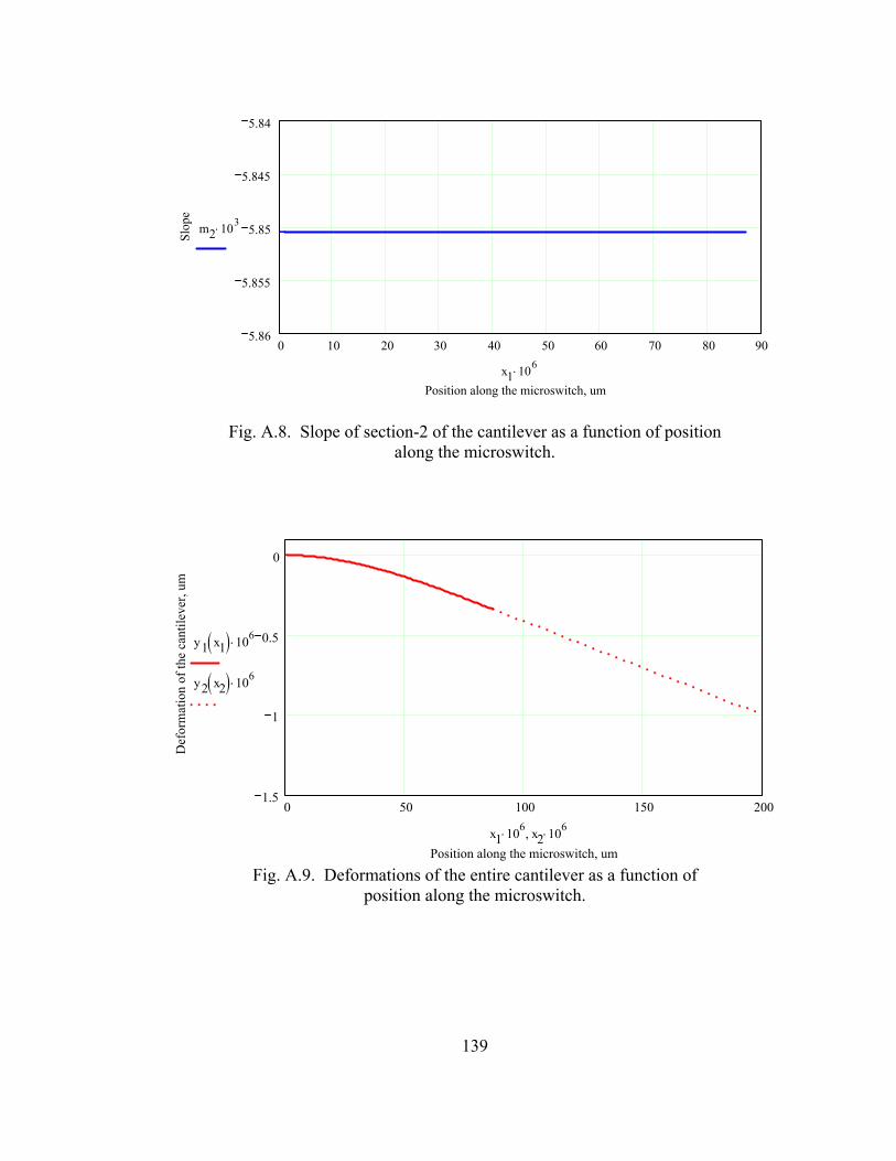
139
0 10 20 30 40 50 60 70 80 905.86
5.855
5.85
5.845
5.84
Position along the microswitch, um
Slop
e
m2 103⋅
x1 106⋅
Fig. A.8. Slope of section-2 of the cantilever as a function of position along the microswitch.
0 50 100 150 200
1.5
1
0.5
0
Position along the microswitch, um
Def
orm
atio
n of
the
cant
ileve
r, um
y1 x1( ) 106⋅
y2 x2( ) 106⋅
x1 106⋅ x2 106⋅,
Fig. A.9. Deformations of the entire cantilever as a function of
position along the microswitch.
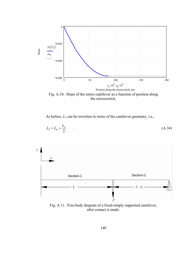
140
0 50 100 150 2000.006
0.004
0.002
0
Position along the microswitch, um
Slop
e
m1 x1( )m2
x1 106⋅ x2 106⋅,
Fig. A.10. Slope of the entire cantilever as a function of position along
the microswitch.
As before, L1 can be rewritten in terms of the cantilever geometry, i.e.,
.
21e
oLLL += (A.34)
Fig. A.11. Free-body diagram of a fixed-simply supported cantilever,
after contact is made.
Section-1
x
L
y
F
L - L1
Section-2
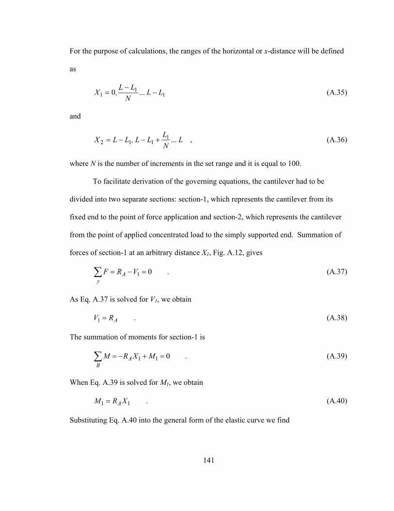
141
For the purpose of calculations, the ranges of the horizontal or x-distance will be defined
as
11
1 ...0 LLN
LL,X −−
= (A.35)
and
LNLLL,LLX ...1
112 +−−= , (A.36)
where N is the number of increments in the set range and it is equal to 100.
To facilitate derivation of the governing equations, the cantilever had to be
divided into two separate sections: section-1, which represents the cantilever from its
fixed end to the point of force application and section-2, which represents the cantilever
from the point of applied concentrated load to the simply supported end. Summation of
forces of section-1 at an arbitrary distance X1, Fig. A.12, gives
.01 =−=∑ VRF Ay
(A.37)
As Eq. A.37 is solved for V1, we obtain
.1 ARV = (A.38)
The summation of moments for section-1 is
.011∑ =+−=B
A MXRM (A.39)
When Eq. A.39 is solved for M1, we obtain
.11 XRM A= (A.40)
Substituting Eq. A.40 into the general form of the elastic curve we find
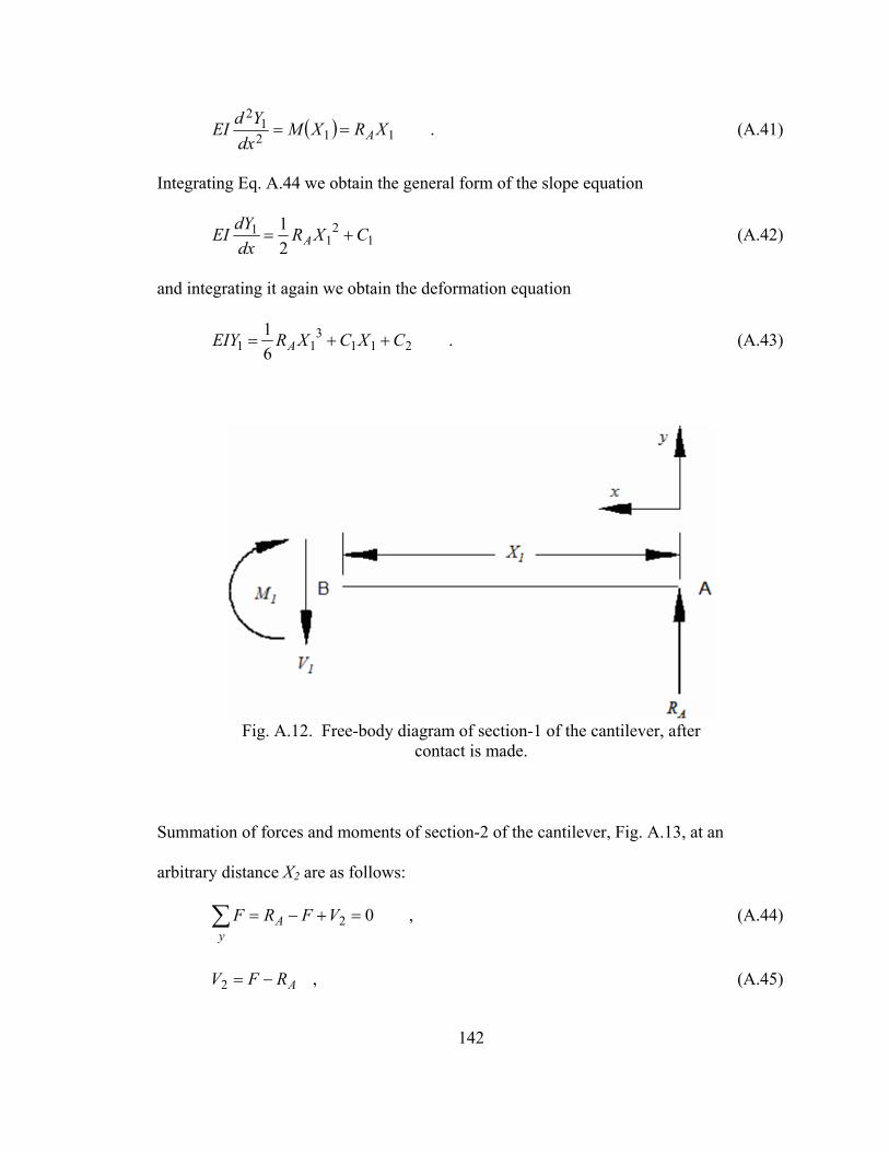
142
( ) .112
12
XRXMdx
YdEI A== (A.41)
Integrating Eq. A.44 we obtain the general form of the slope equation
1
21
121 CXR
dxdYEI A +=
(A.42)
and integrating it again we obtain the deformation equation
.
61
2113
11 CXCXREIY A ++= (A.43)
Fig. A.12. Free-body diagram of section-1 of the cantilever, after
contact is made.
Summation of forces and moments of section-2 of the cantilever, Fig. A.13, at an
arbitrary distance X2 are as follows:
,02 =+−=∑ VFRF Ay
(A.44)
ARFV −=2 , (A.45)
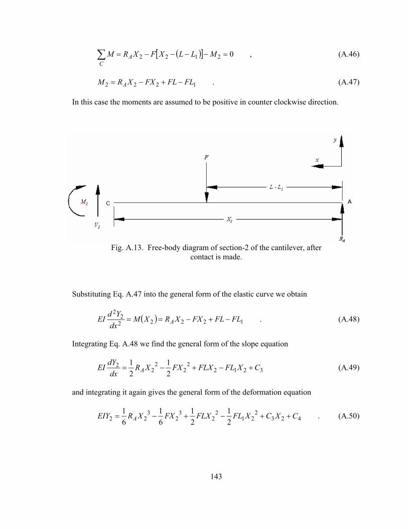
143
( )[ ] ,02122 =−−−−=∑ MLLXFXRM AC
(A.46)
.1222 FLFLFXXRM A −+−= (A.47)
In this case the moments are assumed to be positive in counter clockwise direction.
Fig. A.13. Free-body diagram of section-2 of the cantilever, after
contact is made.
Substituting Eq. A.47 into the general form of the elastic curve we obtain
( ) .12222
22
FLFLFXXRXMdx
YdEI A −+−== (A.48)
Integrating Eq. A.48 we find the general form of the slope equation
3212
22
22
221
21 CXFLFLXFXXR
dxdYEI A +−+−= (A.49)
and integrating it again gives the general form of the deformation equation
.
21
21
61
61
4232
212
23
23
22 CXCXFLFLXFXXREIY A ++−+−= (A.50)

144
In order to solve the unknowns in Eqs A.42 and A.43 and Eqs A.49 and A.50 boundary
and continuity conditions have to be applied. The boundary conditions for the cantilever
with the fixed-simply supported ends are
at 01 =X ,01 =Y (A.51)
at LX =2 ,02 =Y (A.52)
and
at LX =2 ,02 =dx
dY (A.53)
while the continuity conditions at the point of force application are
at 121 LLXX −== 21 YY = (A.54)
and
at 121 LLXX −== .21dx
dYdxdY
= (A.55)
Use of Eqs A.51 to A.55 allows determination of all the unknowns in Eqs A.42, A.43,
A.49, and A.50, and they are
,23
12
11 FLLFLC −−= (A.56)
,
21
65 2
13
12 FLLFLC −= (A.57)
,03 =C (A.58)
,04 =C (A.59)
and
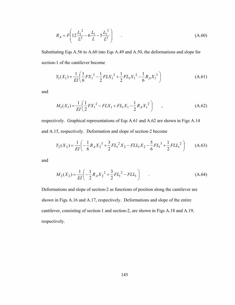
145
.5612 3
311
2
21
⎟⎟⎠
⎞⎜⎜⎝
⎛−−=
LL
LL
LLFRA (A.60)
Substituting Eqs A.56 to A.60 into Eqs A.49 and A.50, the deformations and slope for
section-1 of the cantilever become
⎟⎠⎞
⎜⎝⎛ −+−= 3
12
112
13
111 61
21
21
611)( XRXFLFLXFX
EIXY A
(A.61)
and
,
21
211)( 2
11112
111 ⎟⎠⎞
⎜⎝⎛ −+−= XRXFLFLXFX
EIXM A (A.62)
respectively. Graphical representations of Eqs A.61 and A.62 are shown in Figs A.14
and A.15, respectively. Deformation and slope of section-2 become
⎟⎠⎞
⎜⎝⎛ +−−+−= 2
13
12122
13
222 21
65
23
611)( FLLFLXFLLXFLXR
EIXY A (A.63)
and
.
23
211)( 1
21
2222 ⎟
⎠⎞
⎜⎝⎛ −+−= FLLFLXR
EIXM A (A.64)
Deformations and slope of section-2 as functions of position along the cantilever are
shown in Figs A.16 and A.17, respectively. Deformations and slope of the entire
cantilever, consisting of section-1 and section-2, are shown in Figs A.18 and A.19,
respectively.
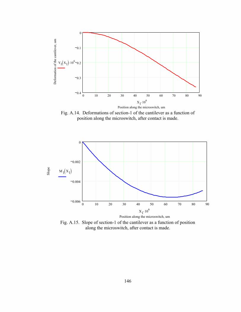
146
0 10 20 30 40 50 60 70 80 900.4
0.3
0.2
0.1
0
Position along the microswitch, um
Def
orm
atio
n of
the
cant
ileve
r, um
Y1 X1( ) 106⋅
X1 106⋅
Fig. A.14. Deformations of section-1 of the cantilever as a function of
position along the microswitch, after contact is made.
0 10 20 30 40 50 60 70 80 900.006
0.004
0.002
0
Position along the microswitch, um
Slop
e
M1 X1( )
X1 106⋅
Fig. A.15. Slope of section-1 of the cantilever as a function of position
along the microswitch, after contact is made.
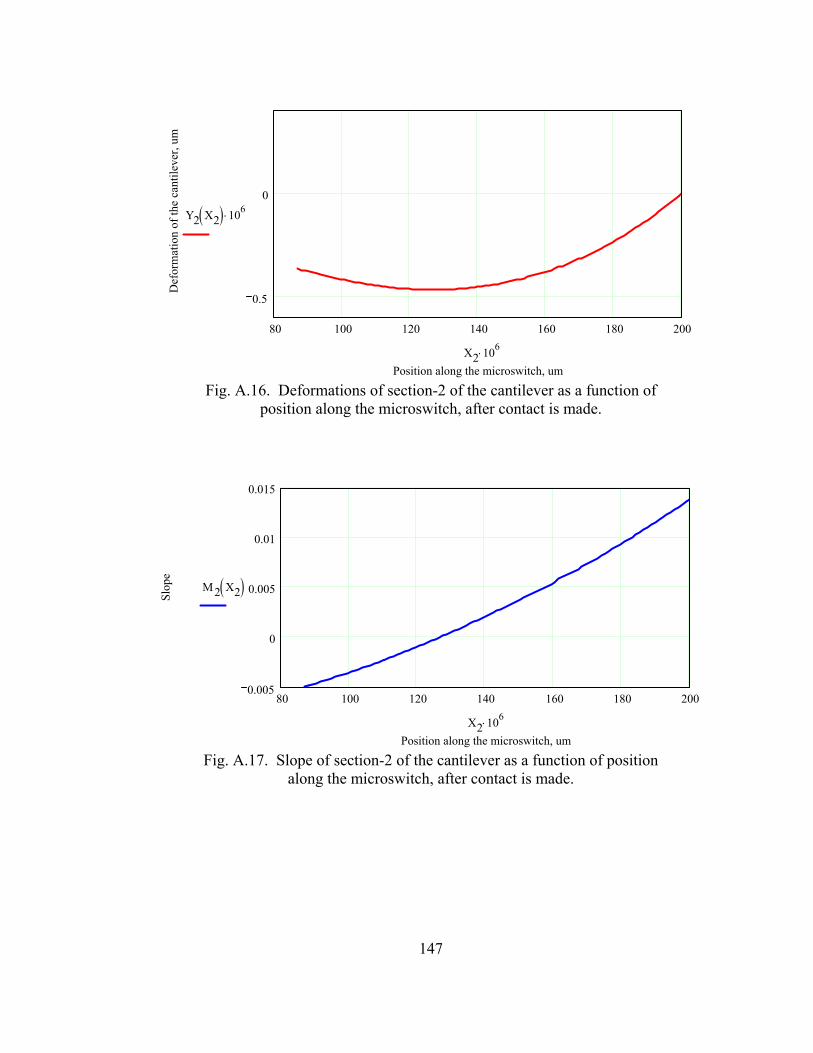
147
80 100 120 140 160 180 200
0.5
0
Position along the microswitch, um
Def
orm
atio
n of
the
cant
ileve
r, um
Y2 X2( ) 106⋅
X2 106⋅
Fig. A.16. Deformations of section-2 of the cantilever as a function of
position along the microswitch, after contact is made.
80 100 120 140 160 180 200
0.005
0
0.005
0.01
0.015
Position along the microswitch, um
Slop
e
M2 X2( )
X2 106⋅
Fig. A.17. Slope of section-2 of the cantilever as a function of position
along the microswitch, after contact is made.
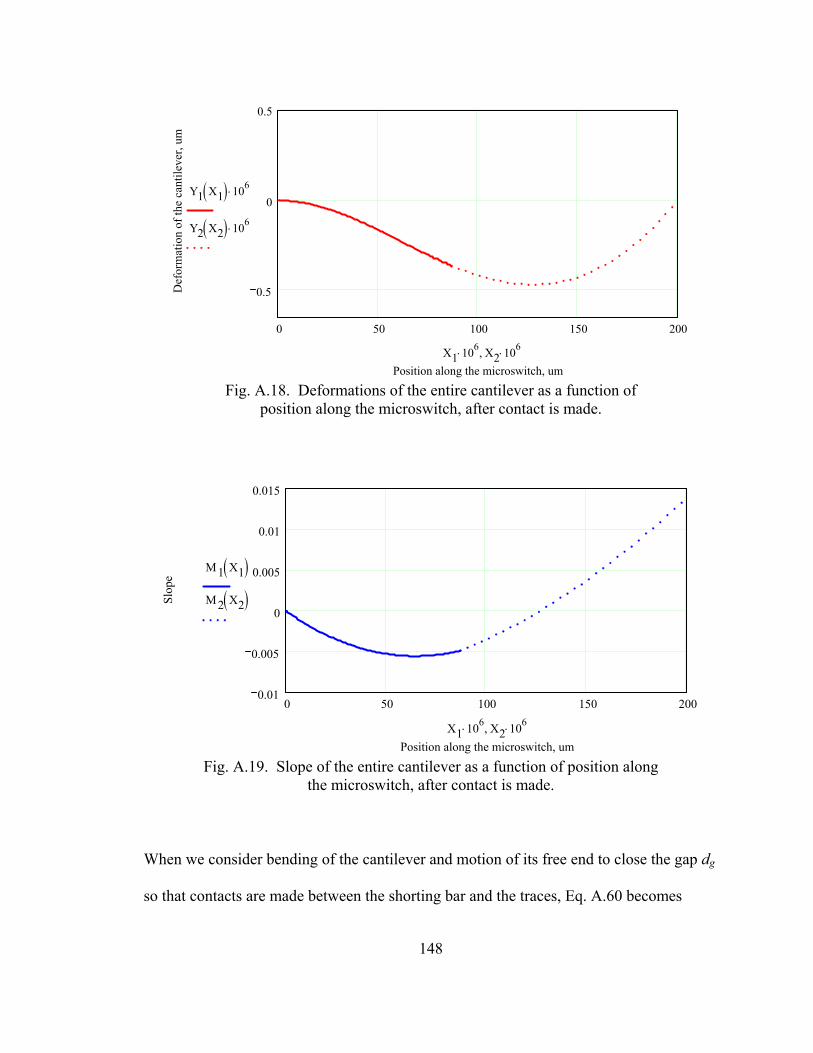
148
0 50 100 150 200
0.5
0
0.5
Position along the microswitch, um
Def
orm
atio
n of
the
cant
ileve
r, um
Y1 X1( ) 106⋅
Y2 X2( ) 106⋅
X1 106⋅ X2 106⋅,
Fig. A.18. Deformations of the entire cantilever as a function of
position along the microswitch, after contact is made.
0 50 100 150 2000.01
0.005
0
0.005
0.01
0.015
Position along the microswitch, um
Slop
e
M1 X1( )M2 X2( )
X1 106⋅ X2 106⋅,
Fig. A.19. Slope of the entire cantilever as a function of position along
the microswitch, after contact is made.
When we consider bending of the cantilever and motion of its free end to close the gap dg
so that contacts are made between the shorting bar and the traces, Eq. A.60 becomes
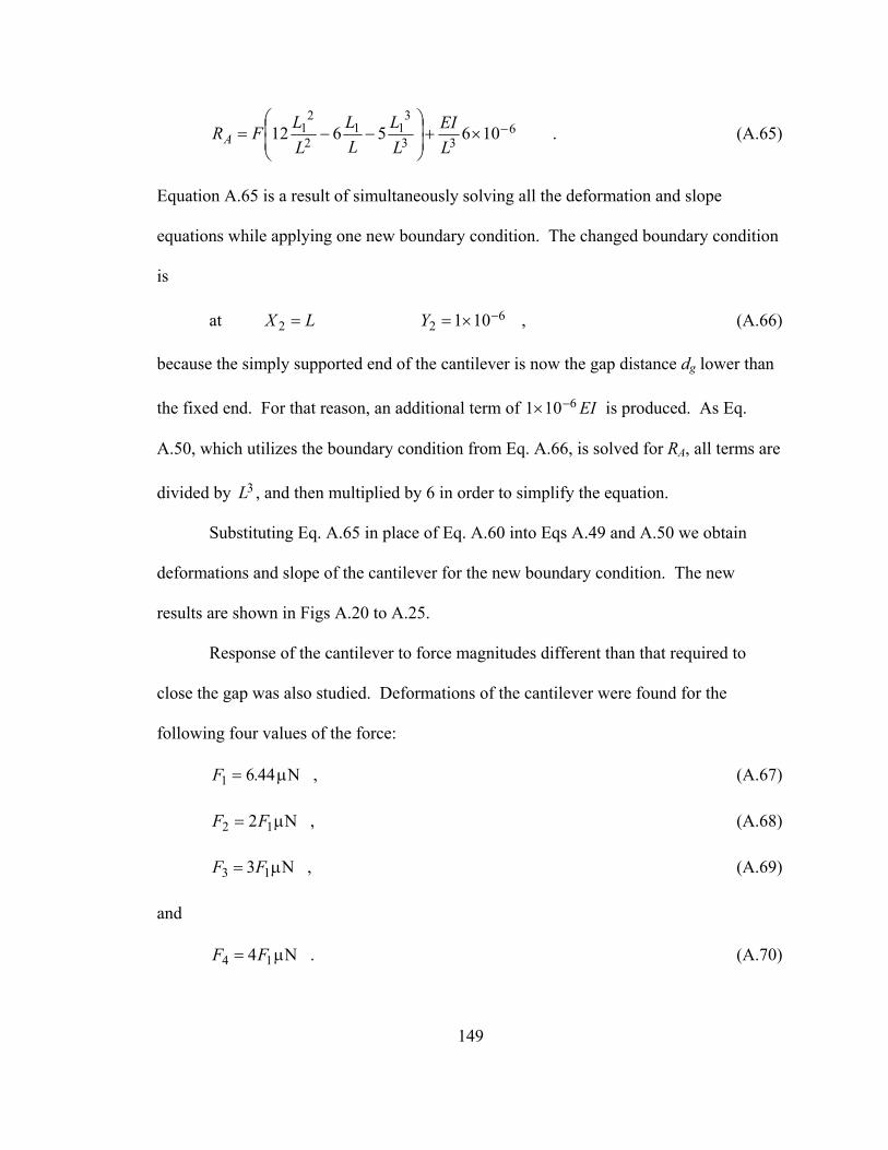
149
.1065612 6
33
311
2
21 −×+⎟
⎟⎠
⎞⎜⎜⎝
⎛−−=
LEI
LL
LL
LLFRA (A.65)
Equation A.65 is a result of simultaneously solving all the deformation and slope
equations while applying one new boundary condition. The changed boundary condition
is
at LX =2 6
2 101 −×=Y
, (A.66)
because the simply supported end of the cantilever is now the gap distance dg lower than
the fixed end. For that reason, an additional term of EI6101 −× is produced. As Eq.
A.50, which utilizes the boundary condition from Eq. A.66, is solved for RA, all terms are
divided by 3L , and then multiplied by 6 in order to simplify the equation.
Substituting Eq. A.65 in place of Eq. A.60 into Eqs A.49 and A.50 we obtain
deformations and slope of the cantilever for the new boundary condition. The new
results are shown in Figs A.20 to A.25.
Response of the cantilever to force magnitudes different than that required to
close the gap was also studied. Deformations of the cantilever were found for the
following four values of the force:
4461 .F = µN , (A.67)
12 2FF = µN , (A.68)
13 3FF = µN , (A.69)
and
14 4FF = µN . (A.70)
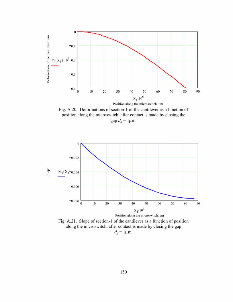
150
0 10 20 30 40 50 60 70 80 900.4
0.3
0.2
0.1
0
Position along the microswitch, um
Def
orm
atio
n of
the
cant
ileve
r, um
Y1 X1( ) 106⋅
X1 106⋅
Fig. A.20. Deformations of section-1 of the cantilever as a function of
position along the microswitch, after contact is made by closing the gap dg = 1µm.
0 10 20 30 40 50 60 70 80 900.008
0.006
0.004
0.002
0
Position along the microswitch, um
Slop
e
M1 X1( )
X1 106⋅
Fig. A.21. Slope of section-1 of the cantilever as a function of position
along the microswitch, after contact is made by closing the gap dg = 1µm.
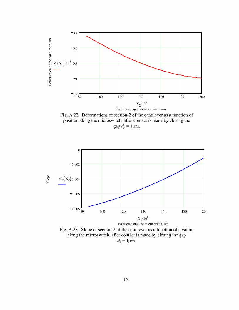
151
80 100 120 140 160 180 2001.2
1
0.8
0.6
0.4
Position along the microswitch, um
Def
orm
atio
n of
the
cant
ileve
r, um
Y2 X2( ) 106⋅
X2 106⋅
Fig. A.22. Deformations of section-2 of the cantilever as a function of
position along the microswitch, after contact is made by closing the gap dg = 1µm.
80 100 120 140 160 180 2000.008
0.006
0.004
0.002
0
Position along the microswitch, um
Slop
e
M2 X2( )
X2 106⋅
Fig. A.23. Slope of section-2 of the cantilever as a function of position
along the microswitch, after contact is made by closing the gap dg = 1µm.
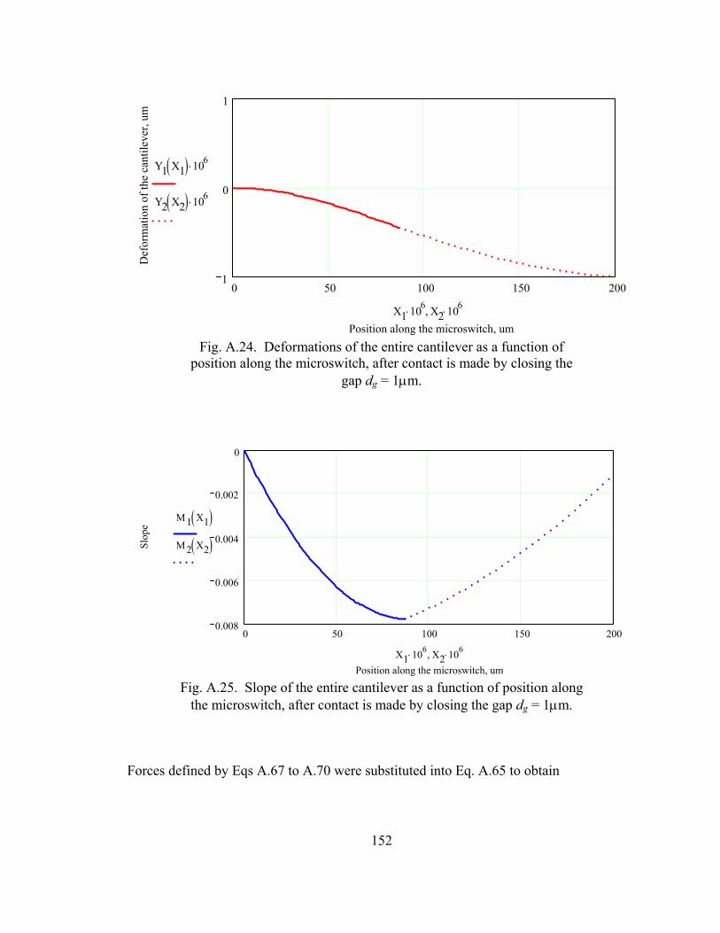
152
0 50 100 150 2001
0
1
Position along the microswitch, um
Def
orm
atio
n of
the
cant
ileve
r, um
Y1 X1( ) 106⋅
Y2 X2( ) 106⋅
X1 106⋅ X2 106⋅,
Fig. A.24. Deformations of the entire cantilever as a function of
position along the microswitch, after contact is made by closing the gap dg = 1µm.
0 50 100 150 200
0.008
0.006
0.004
0.002
0
Position along the microswitch, um
Slop
e
M1 X1( )M2 X2( )
X1 106⋅ X2 106⋅,
Fig. A.25. Slope of the entire cantilever as a function of position along
the microswitch, after contact is made by closing the gap dg = 1µm.
Forces defined by Eqs A.67 to A.70 were substituted into Eq. A.65 to obtain
153
,1065612 6
33
311
2
21
11−×+⎟
⎟⎠
⎞⎜⎜⎝
⎛−−=
LEI
LL
LL
LLFRA (A.71)
,1065612 6
33
311
2
21
22−×+⎟
⎟⎠
⎞⎜⎜⎝
⎛−−=
LEI
LL
LL
LLFRA (A.72)
,1065612 6
33
311
2
21
33−×+⎟
⎟⎠
⎞⎜⎜⎝
⎛−−=
LEI
LL
LL
LLFRA (A.73)
and
.1065612 6
33
311
2
21
44−×+⎟
⎟⎠
⎞⎜⎜⎝
⎛−−=
LEI
LL
LL
LLFRA (A.74)
Substituting Eqs A.71 to A.74 into Eqs A.61 and A.63, the following equations,
representing deformations of section-1 and section-2 of the cantilever due to each force
were obtained:
,
61
21
21
611)( 3
112
1112
113
11111 ⎟⎠⎞
⎜⎝⎛ −+−= XRXLFLXFXF
EIXY A (A.75)
⎟⎠⎞+
⎜⎝⎛ −−+−=
211
311
21122
113
21221
21
65
23
611)(
LLFLF
XLLFXLFXREI
XY A , (A.76)
,
61
21
21
611)( 3
122
1122
123
12112 ⎟⎠⎞
⎜⎝⎛ −+−= XRXLFLXFXF
EIXY A (A.77)
⎟⎠⎞+
⎜⎝⎛ −−+−=
212
312
21222
123
22222
21
65
23
611)(
LLFLF
XLLFXLFXREI
XY A
, (A.78)
154
,
61
21
21
611)( 3
132
1132
133
13113 ⎟⎠⎞
⎜⎝⎛ −+−= XRXLFLXFXF
EIXY A (A.79)
⎟⎠⎞+
⎜⎝⎛ −−+−=
213
313
21322
133
23223
21
65
23
611)(
LLFLF
XLLFXLFXREI
XY A
, (A.80)
,
61
21
21
611)( 3
142
1142
143
14114 ⎟⎠⎞
⎜⎝⎛ −+−= XRXLFLXFXF
EIXY A (A.81)
and
⎟⎠⎞+
⎜⎝⎛ −−+−=
214
314
21422
143
24224
21
65
23
611)(
LLFLF
XLLFXLFXREI
XY A
. (A.82)
Deformations of the cantilever, based on from Eqs A.75 to A.82, as functions of position
along the microswitch are shown in Fig. A.26.
Friction force at the contacts of the microswitch was also studied. To find trends
in friction force behavior, the following range of friction coefficients from Beer and
Johnston (1999) was used:
.6.0...155.0,15.0=µ (A.83)
In order to find the slip forces, slope (i.e. angle) of the cantilever at the point of contact,
Fig. A.27, was determined for all four forces considered. The slope was found by
evaluating Eq. A.64 at X2 = L for each of the four forces found in Eqs A.67 to A.70. The
resulting equations are
,
23
211)( 11
211
221121 ⎟
⎠⎞
⎜⎝⎛ −+−=Θ= LLFLFXR
EILM A (A.84)
155
,
23
211)( 12
212
222222 ⎟
⎠⎞
⎜⎝⎛ −+−=Θ= LLFLFXR
EILM A (A.85)
,
23
211)( 13
213
223323 ⎟
⎠⎞
⎜⎝⎛ −+−=Θ= LLFLFXR
EILM A (A.86)
and
.
23
211)( 14
214
224424 ⎟
⎠⎞
⎜⎝⎛ −+−=Θ= LLFLFXR
EILM A (A.87)
0 20 40 60 80 100 120 140 160 180 2002.5
2
1.5
1
0.5
0
F1F2F3F4F1 cont'dF2 cont'dF3 cont'dF4 cont'd
Position along the microswitch, um
Def
orm
atio
n of
the
cant
ileve
r, um
Fig. A.26. Deformations of the cantilever as functions of position
along the microswitch, after contact is made by closing the gap dg = 1µm, for different magnitudes of the actuation force.
156
Fig. A.27. Slip force at the end of the cantilever.
The slip forces at the simply supported end of the cantilever can be found using the
friction force equations. The friction force equation is written as
nS µFF = , (A.88)
where µ is the coefficient of friction and Fn is the normal force, perpendicular to FS. The
slip forces at the contact end of the microswitch for the four forces considered are
,µR(µF AS )(Θcos) 111 = (A.89)
,µR(µF AS )(Θcos) 222 = (A.90)
,µR(µF AS )(Θcos) 333 = (A.91)
and
.)(Θcos) 444 AS µR(µF = (A.92)
The slip forces as functions of coefficient of friction along the microswitch are shown in
Fig. A.28.
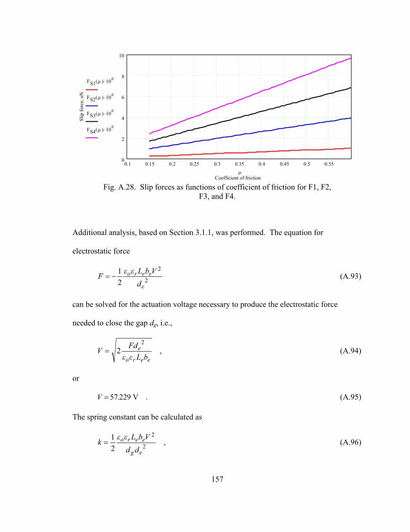
157
0.1 0.15 0.2 0.25 0.3 0.35 0.4 0.45 0.5 0.550
2
4
6
8
10
Coefficient of friction
Slip
forc
e, u
NFS1 µ( ) 106⋅
FS2 µ( ) 106⋅
FS3 µ( ) 106⋅
FS4 µ( ) 106⋅
µ
Fig. A.28. Slip forces as functions of coefficient of friction for F1, F2,
F3, and F4.
Additional analysis, based on Section 3.1.1, was performed. The equation for
electrostatic force
2
2
21
e
eero
dVbLεεF −=
(A.93)
can be solved for the actuation voltage necessary to produce the electrostatic force
needed to close the gap dg, i.e.,
eero
ebLεε
FdV2
2=
, (A.94)
or
V22957.V = . (A.95)
The spring constant can be calculated as
2
2
21
eg
eero
ddVbLεεk =
, (A.96)
158
or
mN441.6=k
. (A.97)
Following the procedure described in Section 3.1.1, the fundamental natural
frequency of the cantilever, considered in this thesis, can be determined based on its
dynamic mass. The dynamic mass of the cantilever can be found to be
,
14033 bhLm ρ= (A.98)
or
g104925 9−×= .m . (A.99)
The natural frequency of the cantilever can be determined as
,
21
mkfo π
= (A.100)
or
.MHz172.010 6 =× −
of (A.101)
The results obtained using Eqs A.93 to A.103 agree with the information obtained
during background research for this thesis. The voltage value obtained from Eq. A.95 is
in the RF MEMS switch operational voltage ranges (Yao and Chang, 1995; Brown,
1998). Similarly, the natural frequency of the cantilever satisfies one of the requirements
for a good microswitch design (Li, et al., 1999; Zou, et al., 2000).

159
APPENDIX B. CALCULATIONS OF TEMPERATURE
160
Equations used in calculating thermal behavior of the microswitch are based on
the following parameters:
current: 310300 −×=I 31050 −×= .δI A
ambient temperature: 298=∞T 2=∞δT K
contact resistance: 1=R 10.δR = Ω
Lorenz number for gold: 81042 −×= .Lr 810050 −×= .δLr
TAS temperature: 8989.TTAS = K .
The voltage-temperature relation in metallic constrictions can be used to calculate
the maximum operating temperature of the microswitch. In order to find this temperature
voltage was calculated according to Ohm’s law, i.e.,
IRV = , (B.1)
3.0=V V . (B.2)
The voltage-temperature relation in metallic constrictions, based on experimental
observations, is written as (Reid and Starman, 2003)
rw L
VTT4
222 =− ∞ . (B.3)
When Eq. B.3 is evaluated for Tw, which represents the maximum operating temperature
of the microswitch, we obtain
22
4 ∞+= TL
VTr
w , (B.4)
310013.1 ×=wT K . (B.5)
161
The maximum temperature of the microswitch was calculated to be 1013°K,
while the results obtained from TAS, Section 4.2.2, showed a maximum temperature of
the microswitch as 716°C or 989°K. In order to find out if the temperature obtained from
the voltage temperature relation in metallic constrictions is in acceptable correlation with
the TAS results, an uncertainty analysis had to be performed.
The maximum temperature of the microswitch obtained from the voltage-
temperature relation depends on three individual parameters: voltage, Lorenz number,
and ambient temperature, i.e., ( )∞TLVT rw ,, . However voltage itself depends on the
electrical current and the resistance, i.e., V = V(I, R). The uncertainty equation for
voltage can be then written as
21
22
⎥⎥⎦
⎤
⎢⎢⎣
⎡⎟⎠⎞
⎜⎝⎛
∂∂
+⎟⎠⎞
⎜⎝⎛
∂∂
= δRRVδI
IVδV , (B.6)
where the partial derivatives are
RIV
=∂∂ (B.7)
and
IRV
=∂∂ . (B.8)
Substituting Eqs B.7 and B.8 into Eq. B.6, we obtain
( ) ( )[ ]2122 δRIδIRδV ⋅+⋅= . (B.9)
General uncertainty equation for the temperature, based on its phenomenological
equation, is
162
21
222
⎥⎥⎦
⎤
⎢⎢⎣
⎡⎟⎟⎠
⎞⎜⎜⎝
⎛∂∂
+⎟⎟⎠
⎞⎜⎜⎝
⎛∂∂
+⎟⎠⎞
⎜⎝⎛
∂∂
= ∞∞δT
TTδL
LTδV
VTδT w
rr
www ,
(B.10)
where the partial derivatives are
21
2
441
−
∞ ⎟⎟⎠
⎞⎜⎜⎝
⎛+=
∂∂ T
LV
LV
VT
rr
w , (B.11)
21
22
2
2
481
−
∞ ⎟⎟⎠
⎞⎜⎜⎝
⎛+−=
∂∂ T
LV
LV
LT
rrr
w , (B.12)
and
21
22
4
−
∞∞∞
⎟⎟⎠
⎞⎜⎜⎝
⎛+=
∂∂ T
LVT
TT
r
w . (B.13)
Substitution of Eqs. B.11 and B.13 into Eq. B.10, yields overall uncertainty in Tw
21
2
21
22
2
21
22
2
2
2
21
22
4
481
441
⎪⎪⎭
⎪⎪⎬
⎫
⎥⎥⎥
⎦
⎤
⎢⎢⎢
⎣
⎡
⎟⎟⎠
⎞⎜⎜⎝
⎛+
+⎥⎥⎥
⎦
⎤
⎢⎢⎢
⎣
⎡
⎟⎟⎠
⎞⎜⎜⎝
⎛+−+
⎪⎩
⎪⎨
⎧
⎥⎥⎥
⎦
⎤
⎢⎢⎢
⎣
⎡
⎟⎟⎠
⎞⎜⎜⎝
⎛+=
∞
−
∞∞
−
∞
−
∞
δTTL
VT
δLTL
VLVδVT
LV
LVδTw
r
rrrrr
(B.14)
or
.K056.99=wTδ (B.15)
To calculate percent overall uncertainty the following equation is used
,100%
w
ww T
TT δδ = (B.16)
163
resulting in
,%189.9% =wTδ (B.17)
In order to find out which parameter has the greatest effect on the overall uncertainty in
the maximum operating temperature of the microswitch percent contributions of the
individual components were calculated according to the following equations:
( )
10044
1
2
2
21
22
w
rr
wδT
δVTL
VLV
VδT%⎥⎥⎥
⎦
⎤
⎢⎢⎢
⎣
⎡
⎟⎟⎠
⎞⎜⎜⎝
⎛+
=
−
∞
δ
, (B.18)
,%923.98=δVT% wδ (B.19)
( )
10048
1
2
2
21
22
2
2
w
rrr
rwδT
δLTL
VLV
LδT%⎥⎥⎥
⎦
⎤
⎢⎢⎢
⎣
⎡
⎟⎟⎠
⎞⎜⎜⎝
⎛+−
=
−
∞
δ
, (B.20)
,%073.1=rw LδT%δ (B.21)
( )
1004
2
2
21
22
w
r
wδT
δTTL
VT
TδT%⎥⎥⎥
⎦
⎤
⎢⎢⎢
⎣
⎡
⎟⎟⎠
⎞⎜⎜⎝
⎛+
=
∞
−
∞∞
∞δ
, (B.22)
and
.%10997.3 3−∞ ×=TT% wδδ (B.23)
In order to check if the calculations of the individual percent contributions are correct, the
results of Eqs B.18 to B.23 were summed to verify that they add to 100%
164
.100=++ ∞TT%LT%VT% wrww δδδδδδ (B.24)
Voltage was calculated to be the greatest contributor to the overall uncertainty in the
maximum operating temperature of the microswitch. Since voltage is a parameter that
depends on the individual uncertainties of electrical current and contact resistance, further
analysis was performed. The percent contribution to the overall uncertainty in voltage
was calculated using the following equations:
( )( )
,1002
2
δVIRIV% δδδ = (B.25)
resulting in
,%028.0% =IVδδ (B.26)
and
( )( )
,1002
2
δVRIRV% δδδ = (B.27)
resulting in
.%972.99% =RVδδ (B.28)
The greatest contributor to the overall uncertainty in voltage is the uncertainty in
contact resistance. The value of the uncertainty in contact resistance used in this analysis
is equal to 10% of the nominal value of contact resistance. In order to decrease the
uncertainty value in the contact resistance more sophisticated fabrication processes
should be used.

165
In order to find the percent difference between the maximum TAS temperature
and the temperature of the microswitch based on the voltage-temperature relation, the
following equation was utilized:
100⋅⎟⎟⎠
⎞⎜⎜⎝
⎛ −=
TAS
wTASDiff T
TT%T , (B.29)
.%3512.%TDiff = (B.30)
Based on the results shown in Eqs B.1 to B.30, we conclude that the temperature
obtained by using the voltage-temperature relation in metallic constrictions correlates
well with the TAS results, since they agree to within the uncertainty limits.

166
APPENDIX C. UNCERTAINTY ANALYSIS
167
An uncertainty analysis had to be perfumed in order to find out how good are the
results defining deformations of the cantilever. The uncertainty analysis was done for
deformations of section-1 and section-2 of the cantilever, which are expressed, based on
the derivations presented in Appendix A, as follows:
⎟⎠⎞
⎜⎝⎛ −+−= 3
12
112
13
111 61
21
21
611)( XRXFLFLXFX
EIXY A (C.1)
and
⎟⎠⎞
⎜⎝⎛ +−−+−= 2
13
12122
13
222 21
65
23
611)( FLLFLXFLLXFLXR
EIXY A
, (C.2)
where
eo LLL21
1 += (C.3)
and
.1065612 6
33
311
2
21 −×+⎟
⎟⎠
⎞⎜⎜⎝
⎛−−=
LEI
LL
LL
LLFRA (C.4)
In order to calculate the overall uncertainty of the deformations for both sections
of the cantilever, the individual uncertainties of L1 and RA had to be calculated, because
L1 is a function of Lo and Le, and RA is a function of L, L1, E, and I. The moment of
inertia is also dependent on the width, b, and thickness, h, of the cantilever. The
uncertainty in L1 can be written as
21
21
21
1 ⎥⎥⎦
⎤
⎢⎢⎣
⎡⎟⎟⎠
⎞⎜⎜⎝
⎛∂∂
+⎟⎟⎠
⎞⎜⎜⎝
⎛∂∂
= ee
oo
δLLLδL
LLδL . (C.5)
When partial derivatives

168
11 =∂∂
oLL (C.6)
and
211 =
∂∂
eLL (C.7)
are substituted into Eq. C.5 we obtain
( )21
22
1 21
⎥⎥⎦
⎤
⎢⎢⎣
⎡⎟⎠⎞
⎜⎝⎛+= eo δLδLδL . (C.8)
The moment of inertia equation for the cantilever considered in this thesis can be written
as
3121 bhI = (C.9)
and the uncertainty in I can be written as
21
22
⎥⎥⎦
⎤
⎢⎢⎣
⎡⎟⎠⎞
⎜⎝⎛
∂∂
+⎟⎠⎞
⎜⎝⎛
∂∂
= δhhIδb
bIδI . (C.10)
When the partial derivatives
3121 h
bI
=∂∂ (C.11)
and
241 hb
hI
=∂∂ (C.12)
are substituted into Eq. C.10 we obtain

169
21
22
23
41
121
⎥⎥⎦
⎤
⎢⎢⎣
⎡⎟⎠⎞
⎜⎝⎛+⎟
⎠⎞
⎜⎝⎛= δhhbδbhδI . (C.13)
Having calculated the uncertainty in the moment of inertia, the uncertainty in RA can be
found using equation
21
2222
11 ⎥
⎥⎦
⎤
⎢⎢⎣
⎡⎟⎠⎞
⎜⎝⎛
∂∂
+⎟⎠⎞
⎜⎝⎛
∂∂
+⎟⎠⎞
⎜⎝⎛
∂∂
+⎟⎟⎠
⎞⎜⎜⎝
⎛∂∂
= δII
RδEE
RδLL
RδLLRδR AAAA
A . (C.14)
Force was omitted from the uncertainty calculations because it was an assumed value,
therefore it had uncertainty of magnitude zero. When the partial derivatives
3
21
21
1151624
LLF
LF
LLF
LR
−−=∂∂
, (C.15)
644
31
21
3
21 101815624 −×−++−=
∂∂
LEI
LLF
LLF
LLF
LR
,
(C.16)
3
6106LI
ER −×=
∂∂
, (C.17)
and
3
6106LE
ER −×=
∂∂
, (C.18)
are substituted into Eq. C.14 we obtain
170
21
2
36
2
36
26
44
31
21
3
21
2
13
21
21
106106
101815624
151624
⎪⎭
⎪⎬⎫
⎟⎠⎞
⎜⎝⎛ ×+⎟
⎠⎞
⎜⎝⎛ ×
+⎥⎥⎦
⎤
⎢⎢⎣
⎡⎟⎟⎠
⎞⎜⎜⎝
⎛×−++−
+⎪⎩
⎪⎨⎧
⎥⎥⎦
⎤
⎢⎢⎣
⎡⎟⎟⎠
⎞⎜⎜⎝
⎛−−=
−−
−
δILEδE
LI
δLLEI
LLF
LLF
LLF
δLLLF
LF
LLFδRA
. (C.19)
Finally, the uncertainty of the deformations of section-1 can be calculated with the
following equation
21
21
2
11
1
2
11
12
12
12
11
⎥⎥⎦
⎤⎟⎠⎞
⎜⎝⎛
∂∂
+⎟⎟⎠
⎞⎜⎜⎝
⎛∂∂
+⎟⎟⎠
⎞⎜⎜⎝
⎛∂∂
+⎟⎟⎠
⎞⎜⎜⎝
⎛∂∂
+⎟⎠⎞
⎜⎝⎛
∂∂
⎢⎢⎣
⎡+⎟
⎠⎞
⎜⎝⎛
∂∂
=
δLLYδL
LY
δXXYδR
RYδI
IYδE
EYδY A
A
. (C.20)
When the partial derivatives
⎟⎠⎞
⎜⎝⎛ −+−−=
∂∂ 3
12
112
13
121
61
21
21
611 XRXFLFLXFX
IEEY
A
, (C.21)
⎟⎠⎞
⎜⎝⎛ −+−−=
∂∂ 3
12
112
13
121
61
21
21
611 XRXFLFLXFX
EIIY
A
, (C.22)
⎟⎠⎞
⎜⎝⎛−=
∂∂ 3
11
611 X
EIRY
A , (C.23)
⎟⎠⎞
⎜⎝⎛ −+−=
∂∂ 2
11112
11
21
211 XRXFLFLXFX
EIXY
AA
, (C.24)
⎟⎠⎞
⎜⎝⎛=
∂∂ 2
11
1211 FX
EILY
, (C.25)
and
171
⎟⎠⎞
⎜⎝⎛−=
∂∂ 2
11
211 FX
EILY (C.26)
are substituted into Eq. C.20, it becomes
21
22
1
2
12
1
2
12
11112
1
23
1
23
12
112
13
12
23
12
112
13
121
211
211
21
211
611
61
21
21
611
61
21
21
611
⎪⎭
⎪⎬⎫
⎥⎦
⎤⎢⎣
⎡⎟⎠⎞
⎜⎝⎛−+⎥
⎦
⎤⎢⎣
⎡⎟⎠⎞
⎜⎝⎛
+⎥⎦
⎤⎢⎣
⎡⎟⎠⎞
⎜⎝⎛ −+−
+⎥⎦
⎤⎢⎣
⎡⎟⎠⎞
⎜⎝⎛−
+⎥⎦
⎤⎢⎣
⎡⎟⎠⎞
⎜⎝⎛ −+−−
⎪⎩
⎪⎨⎧
+⎥⎦
⎤⎢⎣
⎡⎟⎠⎞
⎜⎝⎛ −+−−=
δLFXEI
δLFXEI
δXXRXFLFLXFXEI
δRXEI
δIXRXFLFLXFXEI
δEXRXFLFLXFXIE
δY
A
A
A
A
. (C.27)
Similarly, the uncertainty in deformations of section-2 can be found using equation
21
22
2
11
2
2
22
22
22
22
22
⎥⎥⎦
⎤⎟⎠⎞
⎜⎝⎛
∂∂
+⎟⎟⎠
⎞⎜⎜⎝
⎛∂∂
+⎟⎟⎠
⎞⎜⎜⎝
⎛∂∂
+⎟⎟⎠
⎞⎜⎜⎝
⎛∂∂
+⎟⎠⎞
⎜⎝⎛
∂∂
⎢⎢⎣
⎡+⎟
⎠⎞
⎜⎝⎛
∂∂
=
δLLYδL
LY
δXXYδR
RYδI
IYδE
EYδY A
A
. (C.28)
As the partial derivatives
⎟⎠⎞
⎜⎝⎛ +−−+−−=
∂∂ 2
13
12122
13
222
21
65
23
611 LLFFLXLLFXFLXR
IEEY
A
, (C.29)
⎟⎠⎞
⎜⎝⎛ +−−+−−=
∂∂ 2
13
12122
13
222
21
65
23
611 LLFFLXLLFXFLXR
EIIY
A
, (C.30)
⎟⎠⎞
⎜⎝⎛−=
∂∂ 3
22
611 X
EIRY
A , (C.31)
172
⎟⎠⎞
⎜⎝⎛ −+−=
∂∂
12
12
22
223
211 LLFFLXR
EIXY
A
, (C.32)
⎟⎠⎞
⎜⎝⎛ +−−=
∂∂
12
12211
22531 LLFFLLXFXFL
EILY
, (C.33)
and
⎟⎠⎞
⎜⎝⎛ +−=
∂∂ 2
1212
211 LFXLF
EILY
, (C.34)
are substituted into Eq. C.28 we obtain
21
22
121
2
112
1221
2
212
12
2
23
2
22
13
12122
13
22
22
13
12122
13
222
211
2531
23
211
611
21
65
23
611
21
65
23
611
⎪⎭
⎪⎬⎫
⎥⎦
⎤⎢⎣
⎡⎟⎠⎞
⎜⎝⎛ +−
+⎥⎦
⎤⎢⎣
⎡⎟⎠⎞
⎜⎝⎛ +−−
+⎥⎦
⎤⎢⎣
⎡⎟⎠⎞
⎜⎝⎛ −+−+⎥
⎦
⎤⎢⎣
⎡⎟⎠⎞
⎜⎝⎛−
+⎥⎦
⎤⎢⎣
⎡⎟⎠⎞
⎜⎝⎛ +−−+−−
+⎩⎨⎧
⎥⎦
⎤⎢⎣
⎡⎟⎠⎞
⎜⎝⎛ +−−+−−=
δLLFXLFEI
δLLLFFLLXFXFLEI
δXLLFFLXREI
δRXEI
δILLFFLXLLFXFLXREI
δELLFFLXLLFXFLXRIE
δY
AA
A
A
. (C.35)
Knowing the values of the dimensions of the cantilever, material properties,
forces, and the uncertainties in all of these, the overall uncertainty can be found. The
values used in this analysis are
b = 20 µm δb = 0.5 µm
h = 2.5 µm δh = 0.125 µm
L = 200 µm δL = 2 µm
Lo = 12 µm δLo = 2 µm
173
Le = 150 µm δLe = 2 µm
E = 160 GPa δE = 5 GPa
eo LLL21
1 +=
16
1 ...1013.1,0 LLX −×= − µm δX1 = 0.25 µm
LLLX ...10139.1, 412
−×−= µm δX2 = 0.25 µm
6104412.6 −×=F N
The overall uncertainty in the deformations of section-1 as a function of position
along the microswitch is shown in Fig. C.1, while the percentage overall uncertainty in
the deformations of section-1 as a function of the position along the microswitch
computed using equation
,100)()()(%
11
1111 ⋅=
XYXYXY δδ (C.36)
is shown in Fig. C.2.
The percent overall uncertainty in deformations of section-1 of the cantilever at
X1=L1 is over 15%. This value is not satisfactory for application purposes, thus the
individual percent contributions to the overall uncertainty in deformations of section-1 of
the cantilever were calculated according to equations
( )( )[ ]
1002
11
23
1612
11212
1213
161
21
11XδY
δEXARXFLFLXFXIEXδEY%
⎥⎦
⎤⎢⎣
⎡⎟⎠⎞
⎜⎝⎛ −+−−
=δ , (C.37)
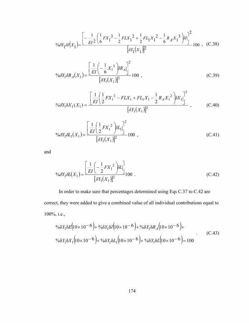
174
( )( )[ ]
1002
11
23
1612
11212
1213
161
21
11%XδY
δIXARXFLFLXFXEIXδIY
⎥⎦
⎤⎢⎣
⎡⎟⎠⎞
⎜⎝⎛ −+−−
=δ , (C.38)
( )( )[ ]
100611
% 211
23
1
11XδY
δRXEI
XδRYA
A
⎥⎦
⎤⎢⎣
⎡⎟⎠⎞
⎜⎝⎛−
=δ , (C.39)
( )[ ]211
2
12
11112
1
11121
211
)(δXδY
δXXRXFLFLXFXEI
XXY%A ⎥
⎦
⎤⎢⎣
⎡⎟⎠⎞
⎜⎝⎛ −+−
=δ , (C.40)
( )( )[ ]
100211
% 211
2
12
1
111XδY
δLFXEI
XLY⎥⎦
⎤⎢⎣
⎡⎟⎠⎞
⎜⎝⎛
=δδ , (C.41)
and
( )( )[ ]
100211
% 211
21
11XδY
δLFXEI
XLY⎥⎦
⎤⎢⎣
⎡⎟⎠⎞
⎜⎝⎛−
=δδ . (C.42)
In order to make sure that percentages determined using Eqs C.37 to C.42 are
correct, they were added to give a combined value of all individual contributions equal to
100%, i.e.,
( ) ( ) ( )( ) ( ) ( ) 10061010δδ%61010δδ%61010δδ%
61010δδ%61010δδ%61010δδ%
11111
111
=−×+−×+−×
+−×+−×+−×
LYLYXY
RYIYEY A
. (C.43)
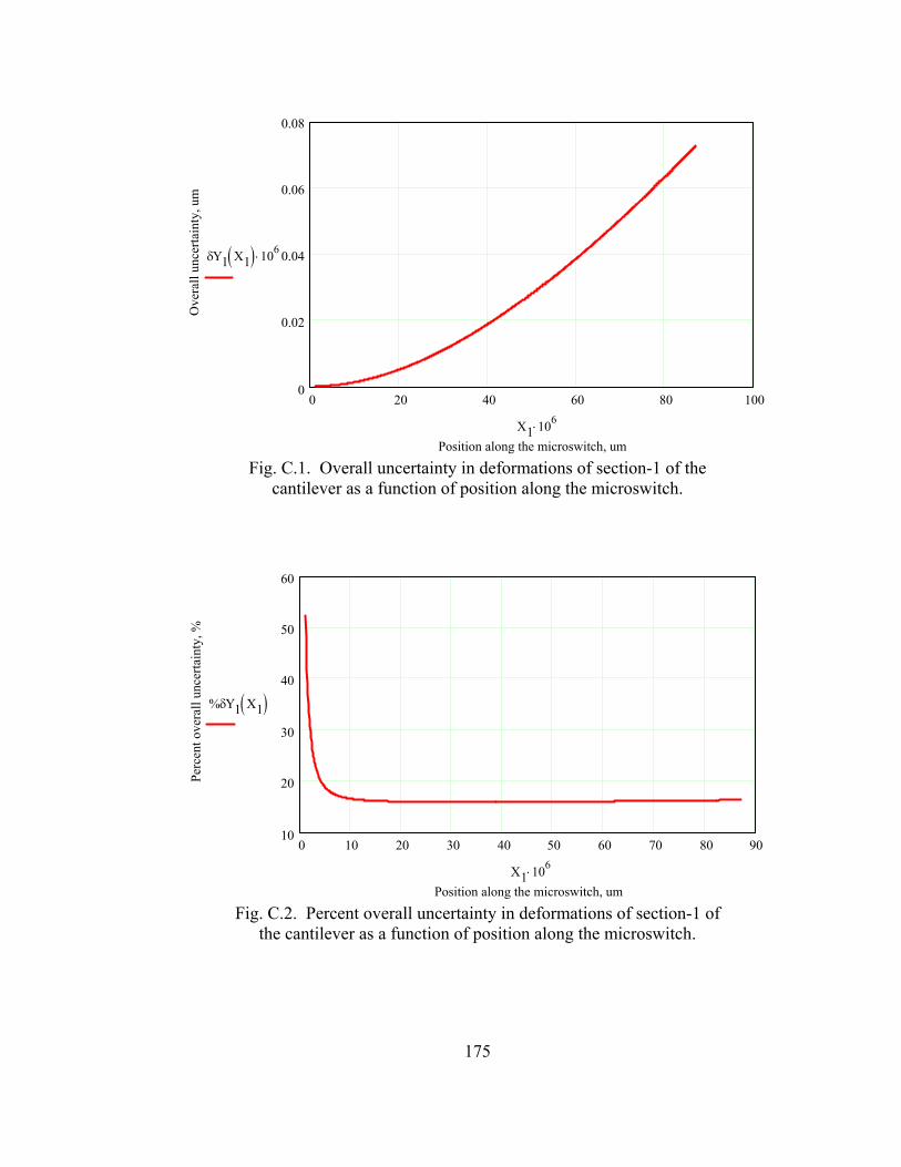
175
0 20 40 60 80 1000
0.02
0.04
0.06
0.08
Position along the microswitch, um
Ove
rall
unce
rtain
ty, u
m
δY1 X1( ) 106⋅
X1 106⋅
Fig. C.1. Overall uncertainty in deformations of section-1 of the
cantilever as a function of position along the microswitch.
0 10 20 30 40 50 60 70 80 9010
20
30
40
50
60
Position along the microswitch, um
Perc
ent o
vera
ll un
certa
inty
, %
%δY1 X1( )
X1 106⋅
Fig. C.2. Percent overall uncertainty in deformations of section-1 of
the cantilever as a function of position along the microswitch.
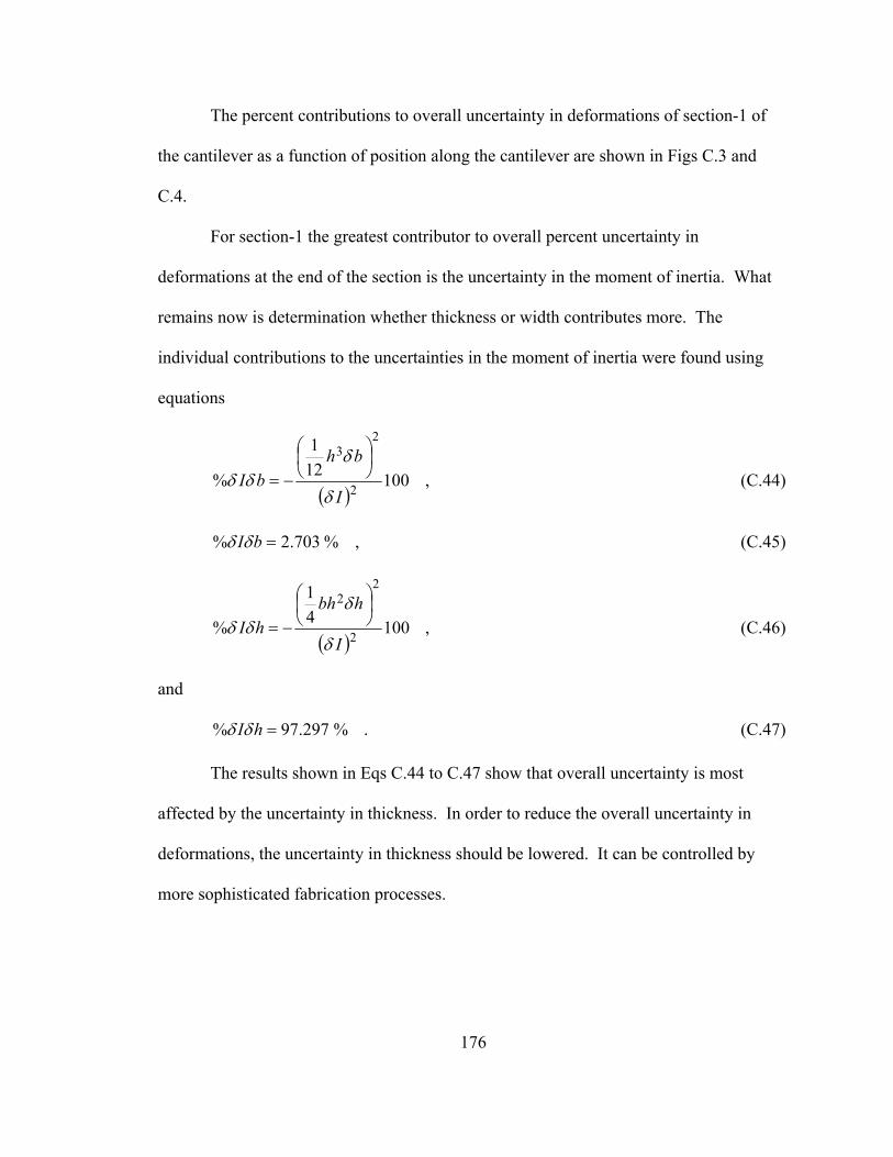
176
The percent contributions to overall uncertainty in deformations of section-1 of
the cantilever as a function of position along the cantilever are shown in Figs C.3 and
C.4.
For section-1 the greatest contributor to overall percent uncertainty in
deformations at the end of the section is the uncertainty in the moment of inertia. What
remains now is determination whether thickness or width contributes more. The
individual contributions to the uncertainties in the moment of inertia were found using
equations
( )10012
1
% 2
23
I
bhbI
δ
δδδ
⎟⎠⎞
⎜⎝⎛
−=
, (C.44)
%703.2% =bIδδ , (C.45)
( )1004
1
% 2
22
I
hbhhI
δ
δδδ
⎟⎠⎞
⎜⎝⎛
−= , (C.46)
and
%297.97% =hIδδ . (C.47)
The results shown in Eqs C.44 to C.47 show that overall uncertainty is most
affected by the uncertainty in thickness. In order to reduce the overall uncertainty in
deformations, the uncertainty in thickness should be lowered. It can be controlled by
more sophisticated fabrication processes.
177
0 20 40 60 80 1000
20
40
60
80
100
Position along the microswitch, um
Perc
ent c
ontri
butio
n, %
%δEY1 X1( )%δIY1 X1( )%δRAY1 X1( )%δX1Y1 X1( )%δL1Y1 X1( )%δLY1 X1( )
X1 106⋅
Fig. C.3. Percent contributions of individual uncertainties to overall
uncertainty in deformations of section-1 of the cantilever as a function of position along the microswitch, lin-lin scale.
0 20 40 60 80 1001 .10 5
1 .10 4
1 .10 3
0.01
0.1
1
10
100
Position along the microswitch, um
Perc
ent c
ontri
butio
n, %
%δEY1 X1( )%δIY1 X1( )%δRAY1 X1( )%δX1Y1 X1( )%δL1Y1 X1( )%δLY1 X1( )
X1 106⋅
Fig. C.4. Percent contributions of individual uncertainties to overall
uncertainty in deformations of section-1 of the cantilever as a function of position along the microswitch, lin-log scale.
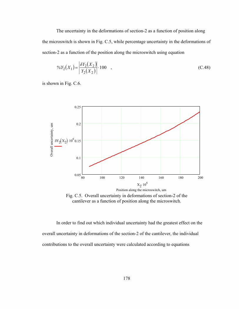
178
The uncertainty in the deformations of section-2 as a function of position along
the microswitch is shown in Fig. C.5, while percentage uncertainty in the deformations of
section-2 as a function of the position along the microswitch using equation
( ) ( )( ) 100
22
2212 ⋅=
XYXδY
X%Y
, (C.48)
is shown in Fig. C.6.
80 100 120 140 160 180 2000.05
0.1
0.15
0.2
0.25
Position along the microswitch, um
Ove
rall
unce
rtain
ty, u
m
δY2 X2( ) 106⋅
X2 106⋅
Fig. C.5. Overall uncertainty in deformations of section-2 of the
cantilever as a function of position along the microswitch.
In order to find out which individual uncertainty had the greatest effect on the
overall uncertainty in deformations of the section-2 of the cantilever, the individual
contributions to the overall uncertainty were calculated according to equations
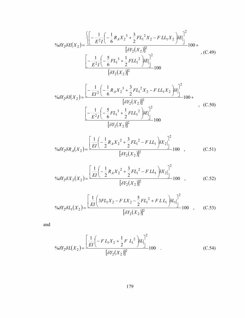
179
( )
( )[ ]
( )[ ]100
21
651
10023
611
%
222
22
13
12
222
2
2122
13
22
22
XδY
δEFLLFLIE
XδY
δEXLLFXFLXRIE
XEYA
⎥⎦
⎤⎢⎣
⎡⎟⎠⎞
⎜⎝⎛ +−−
+⎩⎨⎧
⎥⎦
⎤⎢⎣
⎡⎟⎠⎞
⎜⎝⎛ −+−−
=δδ , (C.49)
( )
( )[ ]
( )[ ]100
21
651
10023
611
%
222
22
13
12
222
2
2122
13
22
22
XδY
δEFLLFLIE
XδY
δIXLLFXFLXREIXIY
A
⎥⎦
⎤⎢⎣
⎡⎟⎠⎞
⎜⎝⎛ +−−
+⎥⎦
⎤⎢⎣
⎡⎟⎠⎞
⎜⎝⎛ −+−−
=δδ , (C.50)
( )( )[ ]
10023
211
% 222
2
212
12
2
22XδY
δXLLFFLXREI
XRYA
A
⎥⎦
⎤⎢⎣
⎡⎟⎠⎞
⎜⎝⎛ −+−
=δδ , (C.51)
( )( )[ ]
10023
211
% 222
2
212
12
2
222XδY
δXLLFFLXREI
XXYA ⎥
⎦
⎤⎢⎣
⎡⎟⎠⎞
⎜⎝⎛ −+−
=δδ , (C.52)
( )( )[ ]
1002531
% 222
2
112
1221
212XδY
δLLLFFLLXFXFLEI
XLY⎥⎦
⎤⎢⎣
⎡⎟⎠⎞
⎜⎝⎛ +−−
=δδ , (C.53)
and
( )( )[ ]
100211
% 222
22
121
22XδY
δLLFXLFEI
XLY⎥⎦
⎤⎢⎣
⎡⎟⎠⎞
⎜⎝⎛ +−
=δδ . (C.54)

180
80 100 120 140 160 180 20016
18
20
22
24
Position along the microswitch, um
Perc
ent o
vera
ll un
certa
inty
, %
%δY2 X2( )
X2 106⋅
Fig. C.6. Percent overall uncertainty in deformations of section-2 of
the cantilever as a function of position along the microswitch.
In order to make sure that percentages determined using Eqs C.49 to C.54 are
correct, they are added to give a combined value of all individual contributions equal to
100%, i.e.,
( ) ( ) ( )( ) ( ) ( ) 10061010δ2δ%610101δ2δ%610102δ2δ%
61010δ2δ%61010δ2δ%61010δ2δ%
=−×+−×+−×
+−×+−×+−×
LYLYXY
ARYIYEY . (C.55)
The percent contributions to overall uncertainty in deformations of section-2 of the
cantilever as a function of position along the microswitch are shown in Figs C.7 and C.8.
For section-2 the greatest contributor to overall percent uncertainty in the
maximum deformation is the uncertainty in the reaction force at the simply supported end
of the cantilever. What remains now is determination whether L1, L, E or I contributes
181
more. The individual contributions to the uncertainties in the reaction force were found
using equations
( )100
151624
% 2
2
13
21
21
1A
AδR
δLLLF
LF
LLF
LR⎥⎥⎦
⎤
⎢⎢⎣
⎡⎟⎟⎠
⎞⎜⎜⎝
⎛−−
=δδ
, (C.56)
%966.4% 1 =LRAδδ , (C.57)
( )100
101815624
% 2
2
644
31
21
3
21
AA
δR
δLLEI
LLF
LLF
LLF
LR⎥⎥⎦
⎤
⎢⎢⎣
⎡⎟⎟⎠
⎞⎜⎜⎝
⎛×−++−
=
−
δδ
, (C.58)
%174.7% =LRAδδ , (C.59)
( )100
106% 2
2
36
AA
δR
δELI
ER⎥⎦
⎤⎢⎣
⎡⎟⎠⎞
⎜⎝⎛ ×
=
−
δδ
, (C.60)
%560.3% =ERAδδ , (C.61)
( )100
106% 2
2
36
AA
δR
δILE
IR⎥⎦
⎤⎢⎣
⎡⎟⎠⎞
⎜⎝⎛ ×
=
−
δδ
, (C.62)
%300.84% =IRAδδ . (C.63)
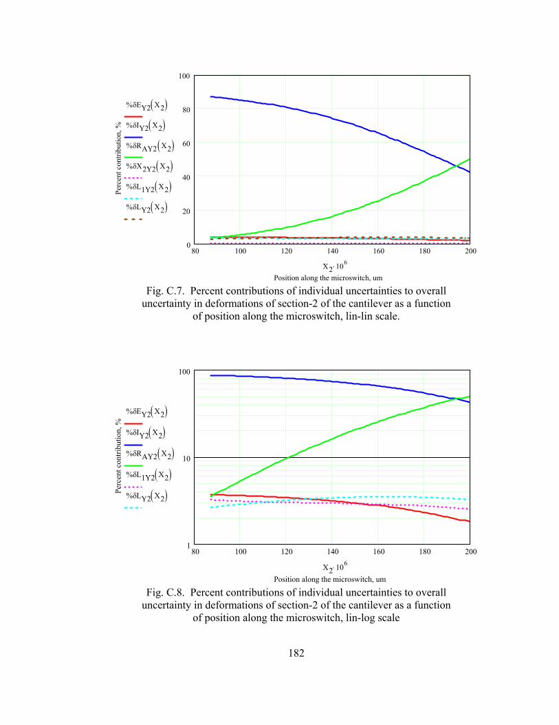
182
80 100 120 140 160 180 2000
20
40
60
80
100
Position along the microswitch, um
Perc
ent c
ontri
butio
n, %
%δEY2 X2( )%δIY2 X2( )%δRAY2 X2( )%δX2Y2 X2( )%δL1Y2 X2( )%δLY2 X2( )
X2 106⋅
Fig. C.7. Percent contributions of individual uncertainties to overall
uncertainty in deformations of section-2 of the cantilever as a function of position along the microswitch, lin-lin scale.
80 100 120 140 160 180 2001
10
100
Position along the microswitch, um
Perc
ent c
ontri
butio
n, %
%δEY2 X2( )%δIY2 X2( )%δRAY2 X2( )%δL1Y2 X2( )%δLY2 X2( )
X2 106⋅
Fig. C.8. Percent contributions of individual uncertainties to overall
uncertainty in deformations of section-2 of the cantilever as a function of position along the microswitch, lin-log scale

183
The results in Eqs C.56 to C.63 show that overall uncertainty in the reaction force
is most affected by the uncertainty in thickness. As the uncertainty in thickness is
reduced to one percent of its nominal value (0.025 µm) the overall uncertainty in the
maximum deformation of the cantilever reduces from over 23% to nearly 11%. Even
though the overall uncertainty in maximum deformation of the cantilever was cut in half,
the uncertainty in thickness remains the greatest contributor to the overall uncertainty in
the reaction force. The reduced value for the uncertainty in thickness is demanding and
expensive to obtain when using currently available MEMS manufacturing processes.
Although it can be further reduced because of advances in fabrication, it may be costly.

184
APPENDIX D. ANALYSIS OF RF CIRCUIT
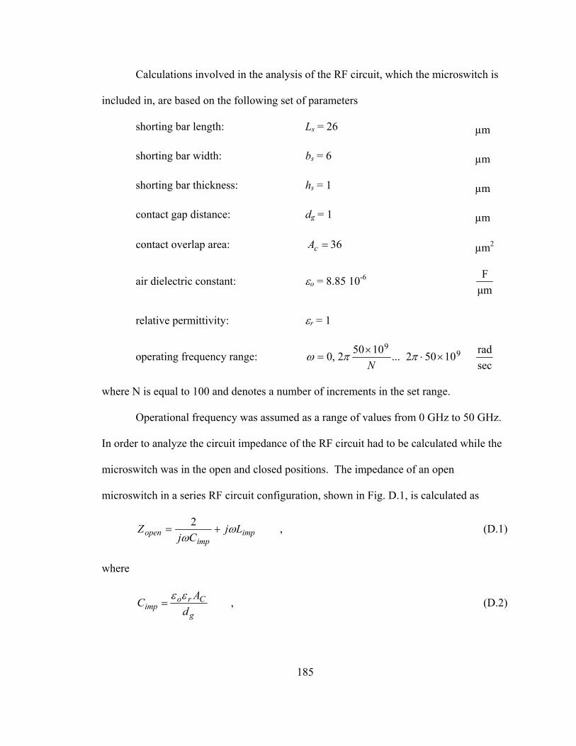
185
Calculations involved in the analysis of the RF circuit, which the microswitch is
included in, are based on the following set of parameters
shorting bar length: Ls = 26 µm
shorting bar width: bs = 6 µm
shorting bar thickness: hs = 1 µm
contact gap distance: dg = 1 µm
contact overlap area: 36=cA µm2
air dielectric constant: εo = 8.85 10-6 µm
F
relative permittivity: εr = 1
operating frequency range: 99
10502...10502,0 ×⋅×
= ππωN
secrad
where N is equal to 100 and denotes a number of increments in the set range.
Operational frequency was assumed as a range of values from 0 GHz to 50 GHz.
In order to analyze the circuit impedance of the RF circuit had to be calculated while the
microswitch was in the open and closed positions. The impedance of an open
microswitch in a series RF circuit configuration, shown in Fig. D.1, is calculated as
,2
impimp
open LjCj
Z ωω
+= (D.1)
where
,
g
Croimp d
AC εε= (D.2)
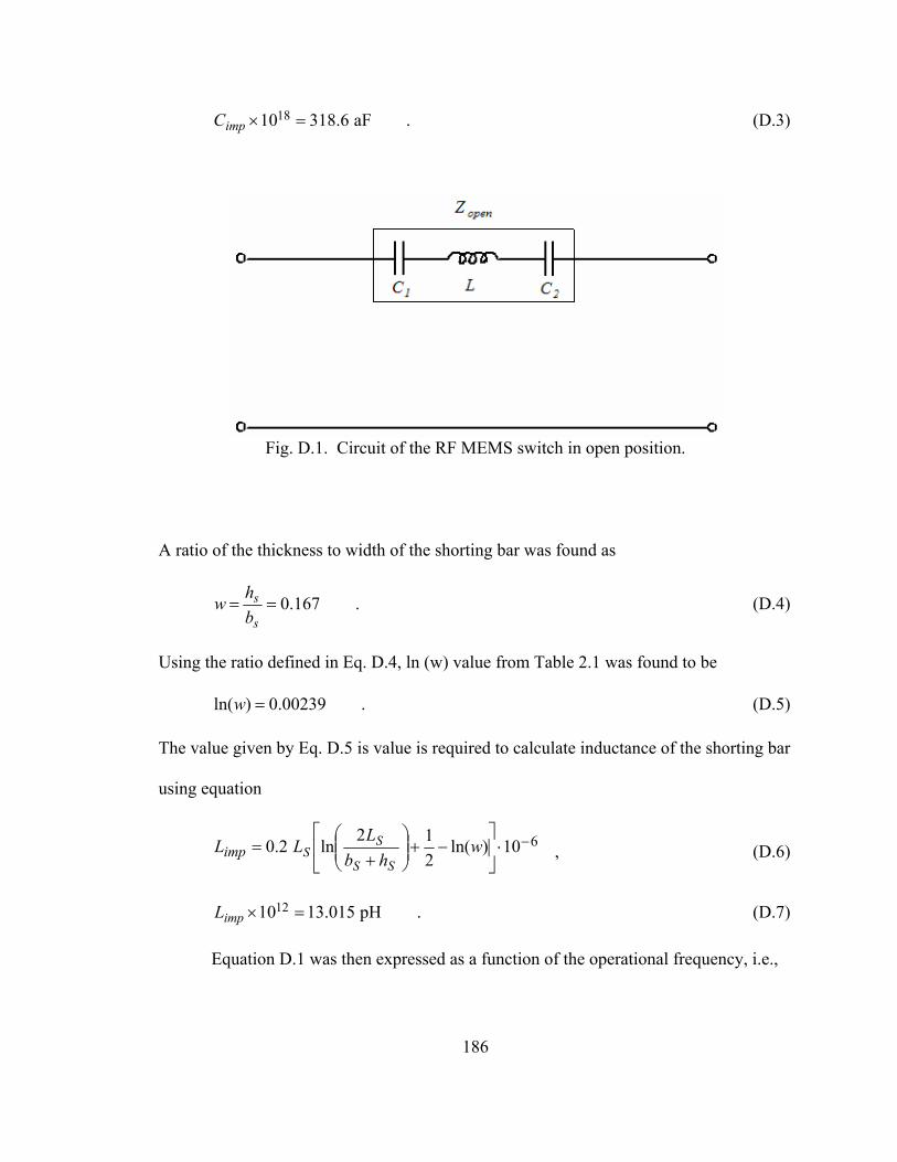
186
.aF6.3181018 =×impC (D.3)
Fig. D.1. Circuit of the RF MEMS switch in open position.
A ratio of the thickness to width of the shorting bar was found as
.167.0==
s
sbhw (D.4)
Using the ratio defined in Eq. D.4, ln (w) value from Table 2.1 was found to be
.00239.0)ln( =w (D.5)
The value given by Eq. D.5 is value is required to calculate inductance of the shorting bar
using equation
610)ln(
212ln2.0 −⋅⎥
⎦
⎤⎢⎣
⎡−+⎟⎟
⎠
⎞⎜⎜⎝
⎛+
= whb
LLLSS
SSimp , (D.6)
.pH015.131012 =×impL (D.7)
Equation D.1 was then expressed as a function of the operational frequency, i.e.,

187
.2)( imp
impopen Lj
CjZ ω
ωω += (D.8)
Graphical representation of the inductance of an open RF MEMS switch as a function of
its operational frequency is given in Fig. D.2.
0.01 0.1 1 10 1000
5000
1 .104
1.5 .104
2 .104
Frequency, GHz
Impe
danc
e, M
ohm
Zopen ω( )
103
ω
2 π⋅
1
109⋅
Fig. D.2. Impedance of the open microswitch as a function of its
operational frequency.
For further analysis, impedance of a closed microswitch in an RF circuit, shown
in Fig. D.3, was computed as
,2 impimpclosed LjRZ ω+= (D.9)
where the contact resistance was assumed to be 1 Ω per contact and the inductance of the
188
shorting bar remained as written in Eq. D.6.
Fig. D.3. Circuit of the RF MEMS switch in closed position.
Equation D.9 was then expressed as a function of the operational frequency, i.e.,
.2)( impimpclosed LjRZ ωω += (D.10)
Graphical representation of inductance of a closed RF MEMS switch as a function of its
operational frequency is shown in Fig. D.4.
Based on the overall design of the circuit, shown in Fig. D.5, the S21 can be found.
Based on information obtained from the Air Force MEMS Research Center an
assumption is made that the impedance of the transition line on both sides of the
microswitch is 50 Ω.
An equation expressing the S21 parameter of an open switch as a function of its
operational frequency is written as
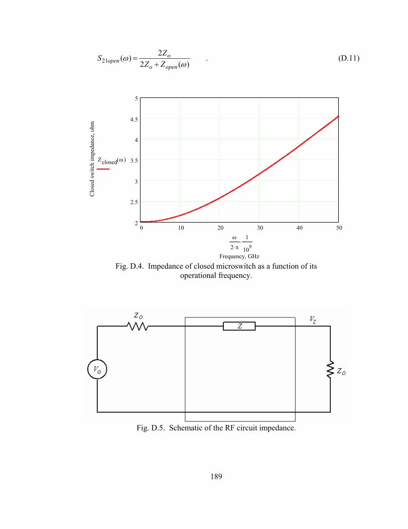
189
.
)(22)(21 ω
ωopeno
oopen ZZ
ZS+
= (D.11)
0 10 20 30 40 502
2.5
3
3.5
4
4.5
5
Frequency, GHz
Clo
sed
switc
h im
peda
nce,
ohm
Zclosed ω( )
ω
2 π⋅
1
109⋅
Fig. D.4. Impedance of closed microswitch as a function of its
operational frequency.
Fig. D.5. Schematic of the RF circuit impedance.
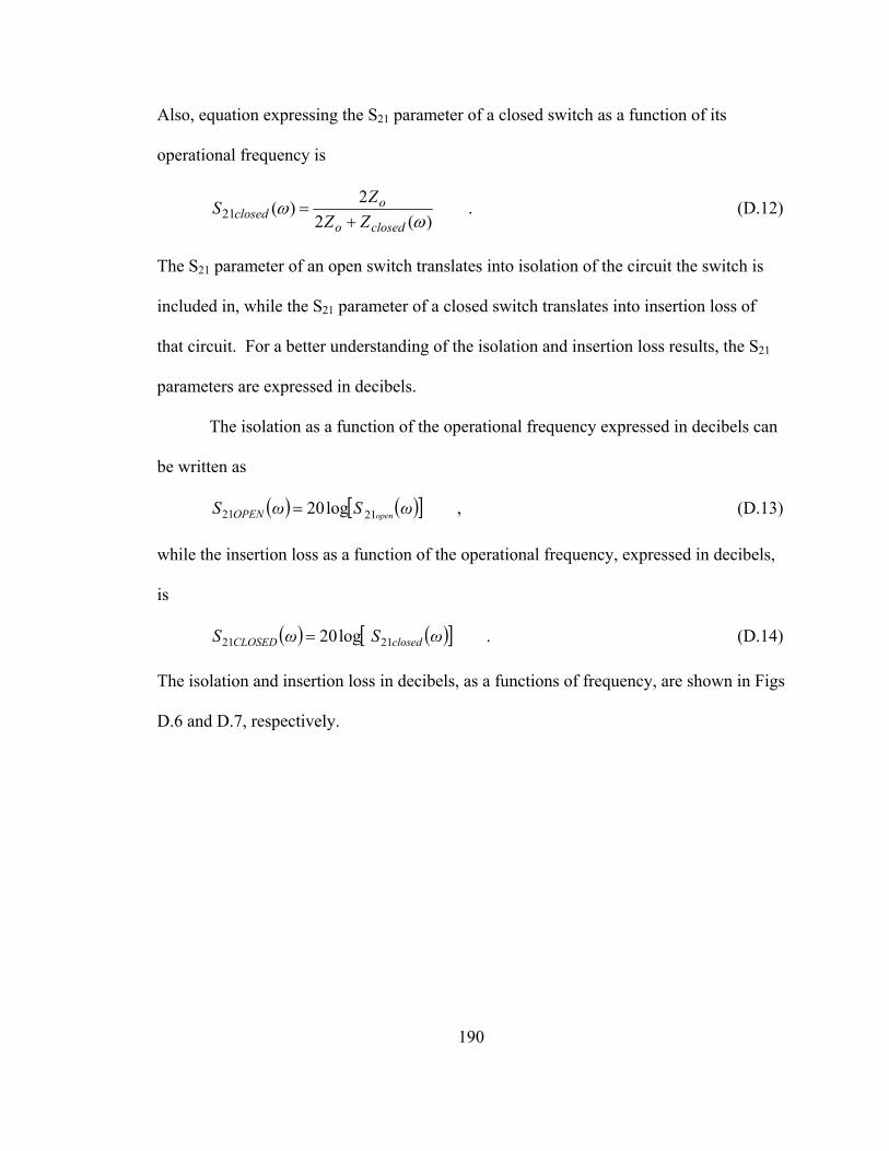
190
Also, equation expressing the S21 parameter of a closed switch as a function of its
operational frequency is
.
)(22)(21 ω
ωclosedo
oclosed ZZ
ZS+
= (D.12)
The S21 parameter of an open switch translates into isolation of the circuit the switch is
included in, while the S21 parameter of a closed switch translates into insertion loss of
that circuit. For a better understanding of the isolation and insertion loss results, the S21
parameters are expressed in decibels.
The isolation as a function of the operational frequency expressed in decibels can
be written as
( ) [ ( )] ,log20 2121 ωSωS openOPEN = (D.13)
while the insertion loss as a function of the operational frequency, expressed in decibels,
is
( ) ( )[ ] .log20 2121 ωSωS closedCLOSED = (D.14)
The isolation and insertion loss in decibels, as a functions of frequency, are shown in Figs
D.6 and D.7, respectively.
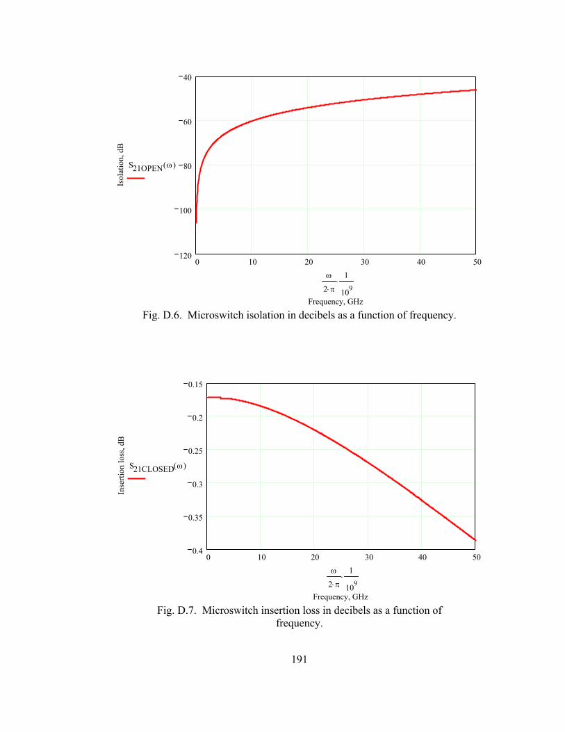
191
0 10 20 30 40 50120
100
80
60
40
Frequency, GHz
Isol
atio
n, d
B
S21OPEN ω( )
ω
2 π⋅
1
109⋅
Fig. D.6. Microswitch isolation in decibels as a function of frequency.
0 10 20 30 40 50
0.4
0.35
0.3
0.25
0.2
0.15
Frequency, GHz
Inse
rtion
loss
, dB
S21CLOSED ω( )
ω
2 π⋅
1
109⋅
Fig. D.7. Microswitch insertion loss in decibels as a function of
frequency.