isscc 2014 / session 13 / advanced embedded memory …swaroopghosh/paper/isscc2014.pdf · isscc...
TRANSCRIPT

230 • 2014 IEEE International Solid-State Circuits Conference
ISSCC 2014 / SESSION 13 / ADVANCED EMBEDDED MEMORY / 13.1
13.1 A 1Gb 2GHz Embedded DRAM in 22nm Tri-Gate CMOS Technology
Fatih Hamzaoglu, Umut Arslan, Nabhendra Bisnik, Swaroop Ghosh,Manoj B. Lal, Nick Lindert, Mesut Meterelliyoz, Randy B. Osborne,Joodong Park, Shigeki Tomishima, Yih Wang, Kevin Zhang
Intel, Hillsboro, OR
CMOS technology scaling continues to drive higher levels of integration in VLSIdesign, which adds more compute engines on a die. To meet the overall performance-scaling needs, high-speed and high-bandwidth memory is becoming increasingly important. Conventional VLSI systems often rely on on-die SRAMs to address the performance gap between CPU and main memory,DRAM. However, with the rapid growth in capacity needs for high-performancememory, SRAM is not always sufficient to meet the demands of bandwidth-intense applications. Embedded DRAM (eDRAM) has been explored as an alternative to satisfy the high-performance and density needs in memory [1-3].In this paper, a high-performance eDRAM based on a 22nm tri-gate CMOS technology is introduced. This eDRAM technology enables the integration of aneDRAM cell into the logic technology platform [4]. The design features a well-balanced configuration to achieve both optimal array efficiency and band-width. By leveraging the high-performance and low-voltage tri-gate transistor at22nm generation, the eDRAM achieves a wide range in operating voltage, from1.1V down to 0.7V, which is essential for low-power logic applications.
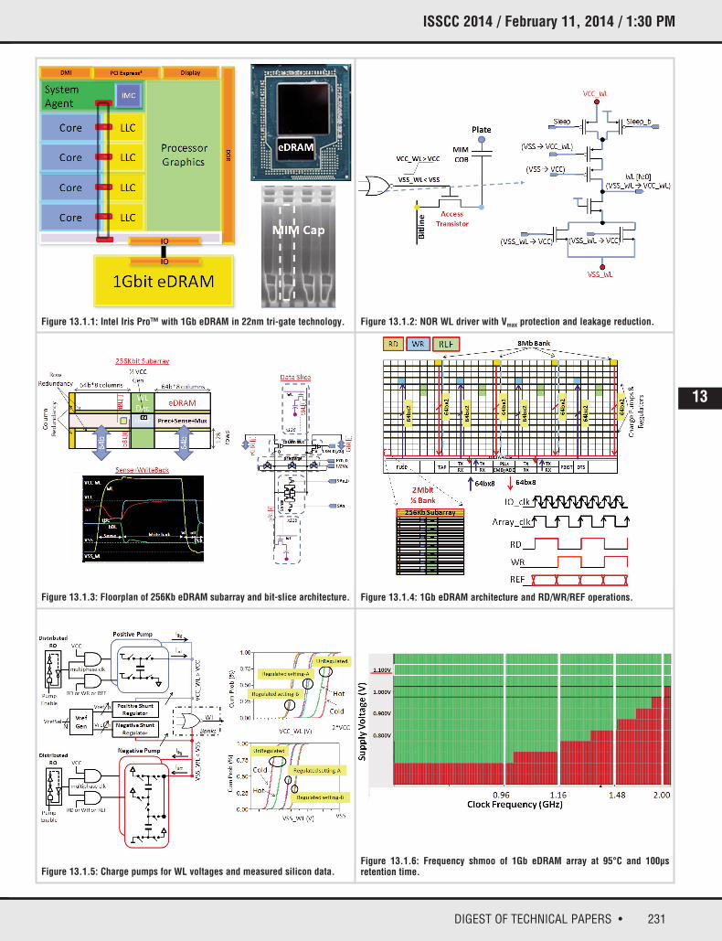
Figure 13.1.1 shows a 4th-generation Core™ processor, where the CPU is connected to a 1Gb eDRAM die through on-package-IO (OPIO) [5]. This multi-chip-package (MCP) product, the Iris Graphics ProTM, uses eDRAM as L4cache and provides low-power high-bandwidth memory access to meet high-performance graphics segment needs. The eDRAM bitcell features a low-leakage access transistor in high-k tri-gate bulk technology and a MIM storagecapacitor with capacitance of greater than 13fF [4,6]. The eDRAM cell area is0.029μm2, less than one-third of the high-density 6T-SRAM bitcell offered in thesame 22nm technology [7], enabling design of high-density memory. The bitcelladopts the capacitor-over-bitline (COB) architecture to maximize the surfacearea of the capacitor. To support high-performance logic in the eDRAM designfor GHz operation, the COB is embedded into the high-performance Cu-metallization interconnect layers. Negative word-line voltage (VSS_WL) withwide programmable range is employed to reduce access-transistor leakage(Fig. 13.1.2). To achieve high data-retention time, VSS_WL and threshold voltage of the access transistor are co-optimized to balance subthreshold leakage and gate-induced drain leakage at the storage node. The access transistor is turned on with the wordline overdriven to VCC_WL by an on-diecharge pump (CP) to allow the storage capacitor to be fully charged to VCC andto achieve fast sensing and data write-back operations. The range of wordlineswing during off and on states is largely determined by the reliability requirement of the access transistor. A NOR-based wordline driver is shown inFig. 13.1.2, where the input signal voltage swings are designed to limit the gatebias to VCC_WL level and below to meet reliability needs. The final WL-drivervoltage for the groups of drivers that are not accessed is kept at VCC in order tominimize the CP loading and leakage power. This design also avoids dual level-shifting circuitry in the same gate, which further reduces the design complexity.
The 256Kb-subarray architecture is shown in Fig. 13.1.3. The array has an open-bitline architecture with 128+ cells on each side, including redundant rows.Similarly, each wordline has a total of 1024+ columns, including redundantcolumns. The subarray achieves 65% area efficiency. The subarray reads orwrites 128+ bits and each bit-slice contains its own set of half-VCC local bitlineprecharge circuitry, sense amplifier, and 8:1 column mux, as described inFig. 13.1.3. Subarrays also contain local half-VCC generators, which are programmable for optimal sensing margin. Four bitcell operations are alsoshown in Fig. 13.1.3, including sense, write-back, wordline-turn-off and local bitline precharge.
Figure 13.1.4 shows the 1Gb array configuration and data-path for read, writeand refresh operations. The chip contains 128 independent banks for read andwrite and 64 bank-groups for refresh, where bank random cycle time (RCT) isequal to six array clock cycles. By providing large number of banks and shortRCT, we minimize bank conflict for high-bandwidth random accesses and maximize performance. Four vertical 256Mb quarters are activated simultaneously during each operation, where each bank reads out 64×2 bits intwo consecutive cycles after column and row repairs to get 512b-wide word size.The OPIO is clocked at twice the array frequency and double data-rate to meetarea and bandwidth requirements. The array has separate data buses for readand write operations but shares a common address bus, hence, it supports readand write operations in alternating array clock cycles to different banks. Therefresh operation can occur during a read or write since it has a separate refreshbank-group address. There are two copies of CPs and regulators, each supporting the top or bottom 512Mb, which occupy less than 2% of the die area.The chip also contains fuses, programmable built-in self test (PBIST), testaccess port (TAP) and a digital thermal sensor (DTS).
Figure 13.1.5 describes the CP circuits that support wordline over- and under-drive voltages. A portion of the CPs always run to support leakage and theremaining portions are activated only when there is array access (read, write orrefresh) to compensate the wordline-activation charge. Although positive andnegative CPs can generate up to 2*VCC and –(VCC/2) output voltages, respectively, output voltages are regulated to a programmable value through on-die-generated reference voltages. The cumulative distribution of both VCC_WLand VSS_WL measurement data at hot (95°C) and cold (-10°C) are also shownin Fig. 13.1.5 for unregulated and two different regulator setting cases. Silicondata show that regulated voltages have less die-to-die variation and better control across temperatures. By introducing programming control over the CPoutput voltages, the design is able to provide a large window to compensateprocess and temperature variation while achieving a balance between performance and reliability.
Figure 13.1.6 shows the voltage-frequency shmoo of the 1Gb eDRAM array tested at 95°C and 100μs retention time. The design achieves 2GHz operationfrequency at a supply voltage of 1.05V, hence 3ns of RCT. The array also supports a wide range in power supply, down to 0.7V at 1GHz frequency.
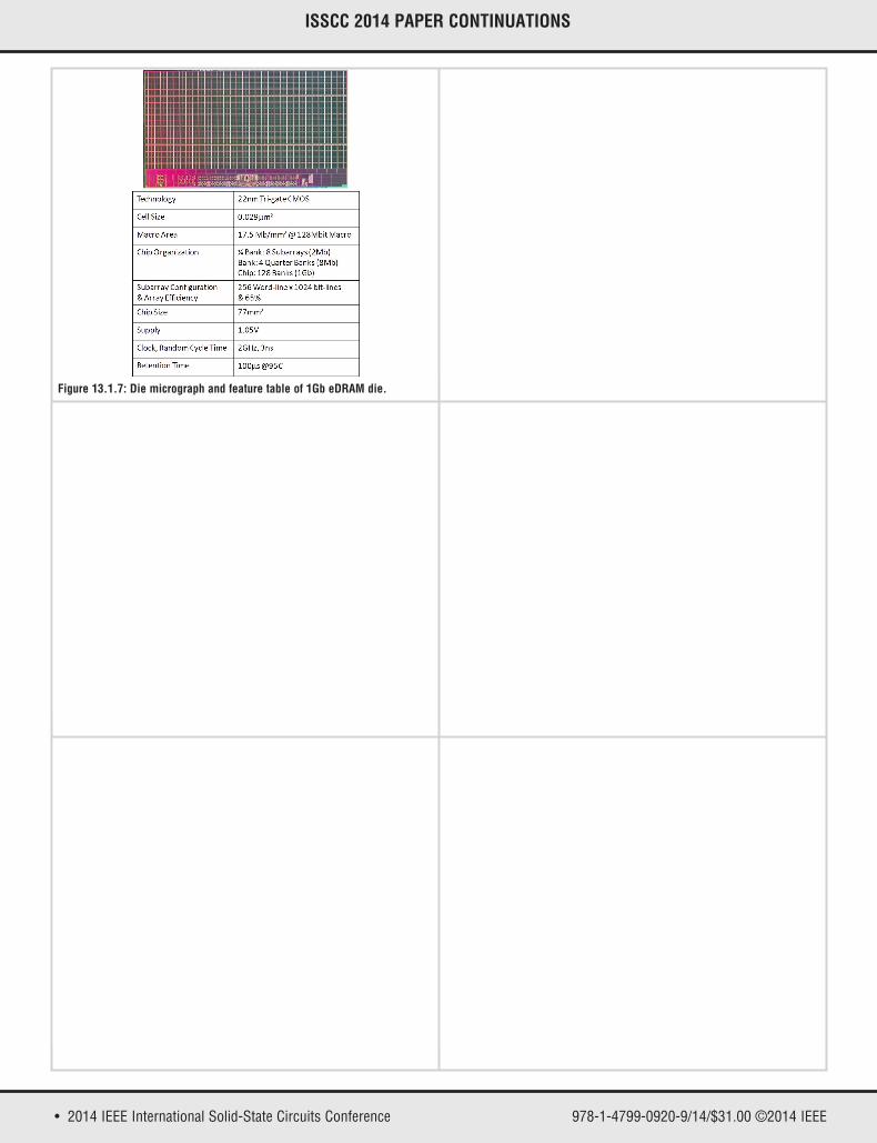
Figure 13.1.7 shows die micrograph of the 1Gb eDRAM and the feature summary table. The chip is fabricated in a 22nm high-performance tri-gateCMOS technology. The die size is 77mm2 with 0.029μm2 eDRAM bitcell area andan array density of 17.5Mb/mm2 at the 128Mb macro level.
Acknowledgements: The authors gratefully acknowledge many members of PTD and IDG technicalstaffs for their contributions to this work.
References:[1] J. Barth et al., “A 45nm SOI Embedded DRAM Macro for POWER7™ 32MBOn-Chip L3 Cache”, ISSCC Dig. Tech. Papers, pp. 342-344, Feb. 2010.[2] K. Hijioka et al., “A Novel Cylinder-Type MIM Capacitor in Porous Low-k Film(CAPL) for Embedded DRAM with Advanced CMOS Logics,” IEDM TechnicalDigest, pp. 756-759, Dec. 2010.[3] S. Romanovsky et al., “A 500MHz Random-Access Embedded 1Mb DRAMMacro in Bulk CMOS”, ISSCC Dig. Tech. Papers, pp. 270-271, Feb. 2008. [4] R. Brain et al., “A 22nm High Performance Embedded DRAM SoCTechnology Featuring Tri-Gate Transistors and MIMCAP COB”, VLSI Tech.Symp., June 2013.[5] N. Kurd et al., “Haswell: A Family of IA 22nm Processors,” ISSCC Dig. Tech.Papers, Feb. 2014[6] Y. Wang et al., “Retention Time Optimization for eDRAM in 22nm Tri-GateCMOS Technology,” IEDM Technical Digest, Dec. 2013.[7] E. Karl et al., “A 4.6GHz, 162Mb SRAM Design in 22nm Tri-Gate CMOSTechnology with Integrated Active Vmin-Enhancing Assist Circuitry,” ISSCC Dig.Tech. Papers, pp. 230-232, Feb. 2012.
978-1-4799-0920-9/14/$31.00 ©2014 IEEE
231DIGEST OF TECHNICAL PAPERS •
ISSCC 2014 / February 11, 2014 / 1:30 PM
Figure 13.1.1: Intel Iris Pro™ with 1Gb eDRAM in 22nm tri-gate technology. Figure 13.1.2: NOR WL driver with Vmax protection and leakage reduction.
Figure 13.1.3: Floorplan of 256Kb eDRAM subarray and bit-slice architecture.
Figure 13.1.5: Charge pumps for WL voltages and measured silicon data.Figure 13.1.6: Frequency shmoo of 1Gb eDRAM array at 95°C and 100µs retention time.
Figure 13.1.4: 1Gb eDRAM architecture and RD/WR/REF operations.
13
• 2014 IEEE International Solid-State Circuits Conference 978-1-4799-0920-9/14/$31.00 ©2014 IEEE
ISSCC 2014 PAPER CONTINUATIONS
Figure 13.1.7: Die micrograph and feature table of 1Gb eDRAM die.