intense pulsed light sintering of copper nanoink for printed electronics · intense pulsed light...
TRANSCRIPT

Appl Phys A (2009) 97: 791–798DOI 10.1007/s00339-009-5360-6
Intense pulsed light sintering of copper nanoink for printedelectronics
Hak-Sung Kim · Sanjay R. Dhage · Dong-Eun Shim ·H. Thomas Hahn
Received: 19 May 2009 / Accepted: 22 July 2009 / Published online: 5 August 2009© The Author(s) 2009. This article is published with open access at Springerlink.com
Abstract An intense pulsed light (IPL) from a xenon flashlamp was used to sinter copper nanoink printed on low-temperature polymer substrates at room temperature in am-bient condition. The IPL can sinter the copper nanoink with-out damaging the polymer substrates in extremely short time(2 ms). The microstructure of the sintered copper film wasinvestigated using X-ray powder diffraction (XRD), opti-cal microscopy, scanning electron microscopy (SEM), X-raymicro tomography, and atomic force microscopy (AFM).The sintered copper film has a grainy structure with neck-like junctions. The resulting resistivity was 5 µ� cm of elec-trical resistivity which is only 3 times as high as that of bulkcopper. The IPL sintering technique allows copper nanopar-ticles to be used in inkjet printing on low-temperature sub-strates such as polymers in ambient conditions.
PACS 71.20.Gj · 72.15.-v · 73.22.Dj · 73.61.At · 81.20.Ev
1 Introduction
Printed electronics techniques such as inkjet printing andflexo-printing present a low-cost solution to the productionof electronic devices such as radio frequency identification
H.-S. Kim (�) · S.R. Dhage · D.-E. Shim · H.T. HahnMechanical and Aerospace Engineering Department, Universityof California, Los Angeles, CA 90095, USAe-mail: [email protected]: +1-310-206-4830
H.T. HahnMaterial Science and Engineering Department, CaliforniaNanoSystems Institute, University of California, Los Angeles,CA 90095, USA
(RFID) tags and large-area displays as they can do awaywith the time consuming and expensive processes inherentin the conventional photolithographic techniques used in thePCB (printed circuit board) industry [1]. Key componentsof printed electronics are conducting lines and films. Al-though conducting polymers could be used for these com-ponents, their conductivity and stability are still much infe-rior to those of their metallic counterparts [2–4]. Therefore,metal-based nanoinks have recently been introduced to al-leviate these shortcomings. For the metal-based nanoinks,the need for low-temperature, in-situ sintering of conductiveelectrodes is an important issue. Kim et al. [2] developedAg nanoparticle ink for inkjet printing where the nanopar-ticles could be sintered at temperatures around 200◦C for30 min. They investigated the resistance changes of theinkjet printed conductive films with respect to the sinter-ing temperature and Ag particle size. Ko et al. [4] stud-ied sintering of gold nanoink on a polymer substrate us-ing a 520-nm laser. They obtained a high line resolutiondown to 1–2 µm with a low resistivity of 5.41 µ� cm, whichis only two times that of bulk gold (2.65 µ� cm). How-ever, this local laser sintering technique requires a sophis-ticated 3D gantry system. In addition, since this techniquecan only sinter very small spots, it is difficult to cover largeareas.
Although novel materials such as silver and gold can besintered at fairly low temperatures, they are too expensiveto be used for mass production. Therefore, Park et al. [3]developed a low-viscosity conductive ink containing well-dispersed copper nanoparticles through a polyol process.The inkjet printed nanoparticles were sintered at 325◦C for1 h in vacuum to prevent oxidation [3]. However, the tra-ditional thermal sintering still requires a high temperature,long cycle time and a vacuum chamber.

792 H.-S. Kim et al.
Fig. 1 Schematic of intensepulsed light sintering system:(a) overall system; (b) xenonflash lamp setup
Flash lamp annealing (FLA) is a millisecond process us-ing irradiation of lights over a broad spectrum in the visiblerange. This technique has been used successfully to mini-mize the annealing cycle for thin gate oxides on a siliconwafer to within a few milliseconds [5, 6]. The techniqueused a halogen lamp for pre-heating of the wafer to 300◦Cand then a xenon flash lamp to increase the wafer tempera-ture to 600–700◦C instantly. The sheet resistance was char-acterized as function of the flash light intensity and preheat-ing temperature to show that the flash lamp annealing is ef-fective for channel engineering in sub 100-nm MOSFETS.Although there are several reports on the application of theFLA technique to the annealing of channels in silicon sub-strates, the literature on the use of intense pulsed light to sin-ter conductive nanoparticles for printed electronics is rare tothe authors’ knowledge.
In the present work, we have developed an intense pulsedlight (IPL) sintering technique for millisecond, large areasintering of copper conductive paths in ambient conditions.Commercial copper nanoink was painted on several poly-mer substrates and sintered using a xenon flash lamp systemunder varying levels of light intensity. The resulting con-ductivity was measured and correlated with microstructuresexamined by atomic force microscopy (AFM), X-ray dif-fraction (XRD), scanning electron microscopy (SEM), andX-ray micro tomography.
2 Experimental procedure
The nanoink has copper particles of 5-nm diameter uni-formly dispersed in a mixed solvent of ethylene glycoland 2-methoxyethanol (Samsung Electro-Mechanic, Korea).About 5 µl of copper nanoink was dropped and spread uni-formly over a square area 10 mm × 10 mm using an autopipette. The solvent was dried out at 80◦C for 10 min and1 µm thick copper particles film was obtained. Also, a rub-ber stamp was used to make a copper nanoink pattern on
Fig. 2 Spectral distribution of a xenon flash lamp [7]
the polymer substrate. For the substrate, four different ma-terials were used: glass fiber BT (bismaleimide triazine)epoxy composite, polyimide film (Kapton, Dupont), poly-ethylene (PE) film, and polypropylene (PP) film. The intensepulsed light (IPL) sintering system was set up as shownin Fig. 1.
The IPL sintering system is composed of a xenon flashlamp (PerkinElmer QXA, UK), an aluminum reflector, apower supply, capacitors, a simmer triggering pulse con-troller, and a light filter. IPL is generated using an arc plasmaphenomenon in the xenon flash lamp [7]. Once the gas isionized, a spark is formed between the electrodes, allow-ing the capacitor current to conduct, which is the arc plasmaphenomenon. A charged super capacitor (40000 µF) is usedto deliver high electrical current (about 1000 A) in a shorttime (1–10 ms) when the lamp is triggered. During the arcplasma generation, the flash lamp emits an optical spectrumof light that covers a wide range of wavelength from 160 nmto 2.5 mm [7]. The conversion of electrical input power intoradiated optical power is approximately 50% in the wave-length range of 200–1100 nm, Fig. 2 [7].
Intense pulsed light sintering of copper nanoink for printed electronics 793
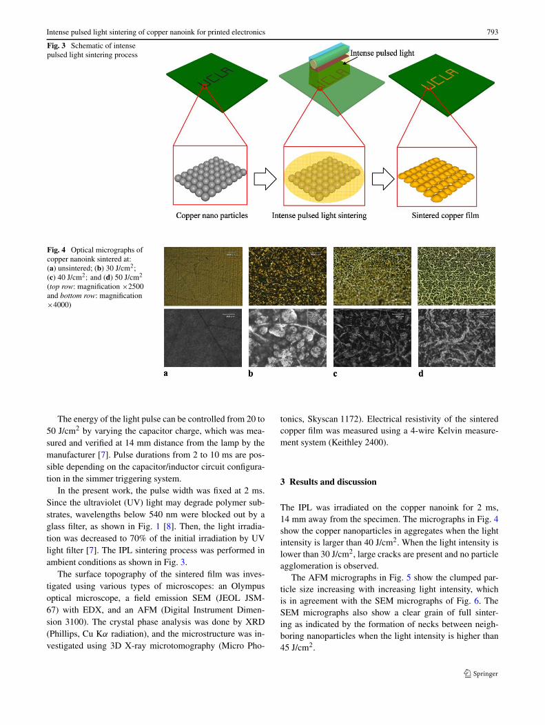
Fig. 3 Schematic of intensepulsed light sintering process
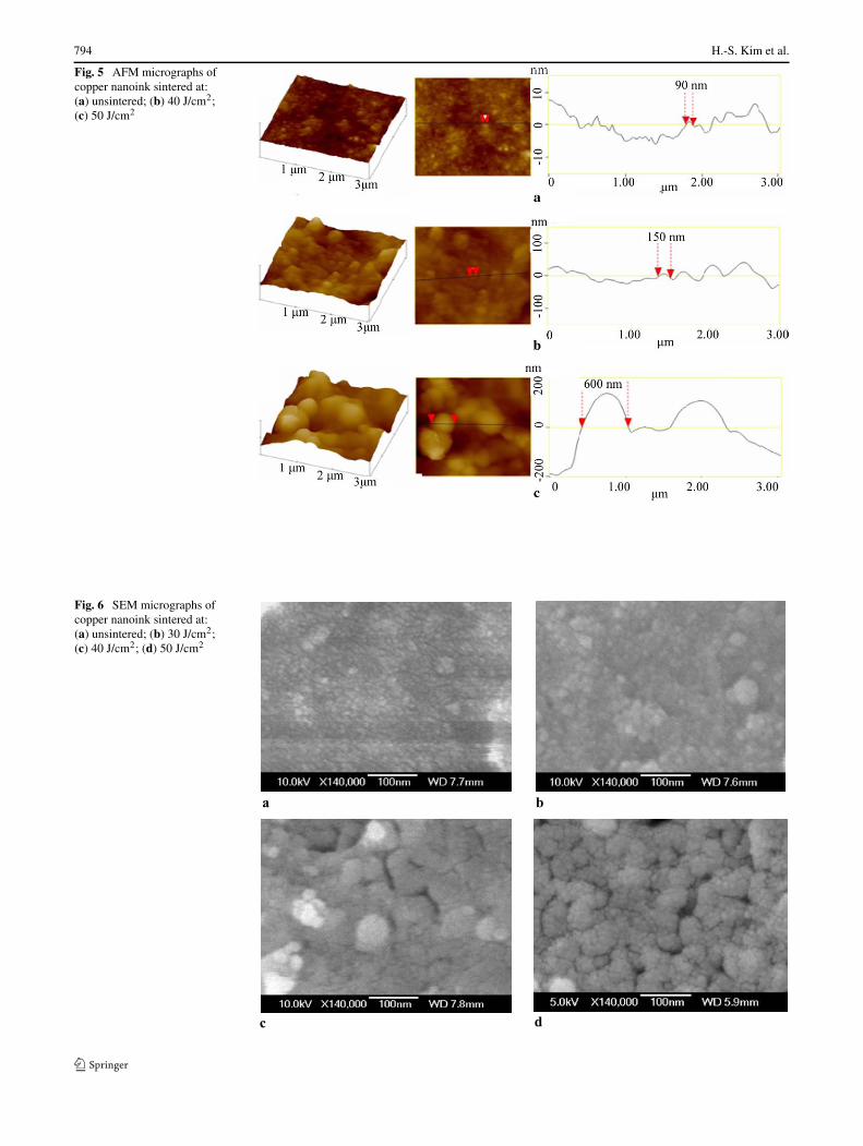
Fig. 4 Optical micrographs ofcopper nanoink sintered at:(a) unsintered; (b) 30 J/cm2;(c) 40 J/cm2; and (d) 50 J/cm2
(top row: magnification ×2500and bottom row: magnification×4000)
The energy of the light pulse can be controlled from 20 to50 J/cm2 by varying the capacitor charge, which was mea-sured and verified at 14 mm distance from the lamp by themanufacturer [7]. Pulse durations from 2 to 10 ms are pos-sible depending on the capacitor/inductor circuit configura-tion in the simmer triggering system.
In the present work, the pulse width was fixed at 2 ms.Since the ultraviolet (UV) light may degrade polymer sub-strates, wavelengths below 540 nm were blocked out by aglass filter, as shown in Fig. 1 [8]. Then, the light irradia-tion was decreased to 70% of the initial irradiation by UVlight filter [7]. The IPL sintering process was performed inambient conditions as shown in Fig. 3.
The surface topography of the sintered film was inves-tigated using various types of microscopes: an Olympusoptical microscope, a field emission SEM (JEOL JSM-67) with EDX, and an AFM (Digital Instrument Dimen-sion 3100). The crystal phase analysis was done by XRD(Phillips, Cu Kα radiation), and the microstructure was in-vestigated using 3D X-ray microtomography (Micro Pho-
tonics, Skyscan 1172). Electrical resistivity of the sinteredcopper film was measured using a 4-wire Kelvin measure-ment system (Keithley 2400).
3 Results and discussion
The IPL was irradiated on the copper nanoink for 2 ms,14 mm away from the specimen. The micrographs in Fig. 4show the copper nanoparticles in aggregates when the lightintensity is larger than 40 J/cm2. When the light intensity islower than 30 J/cm2, large cracks are present and no particleagglomeration is observed.
The AFM micrographs in Fig. 5 show the clumped par-ticle size increasing with increasing light intensity, whichis in agreement with the SEM micrographs of Fig. 6. TheSEM micrographs also show a clear grain of full sinter-ing as indicated by the formation of necks between neigh-boring nanoparticles when the light intensity is higher than45 J/cm2.
794 H.-S. Kim et al.
Fig. 5 AFM micrographs ofcopper nanoink sintered at:(a) unsintered; (b) 40 J/cm2;(c) 50 J/cm2
Fig. 6 SEM micrographs ofcopper nanoink sintered at:(a) unsintered; (b) 30 J/cm2;(c) 40 J/cm2; (d) 50 J/cm2

Intense pulsed light sintering of copper nanoink for printed electronics 795
Fig. 7 EDX spectra of coppernanoink sintered at differentlight intensities
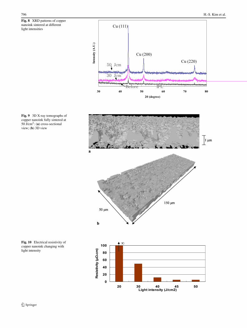
The EDX spectra in Fig. 7 shows the C and O peaks de-creasing as the light intensity increases. In order to ensurethat the O peak is not from the oxidization of copper, XRDpattern of the Cu were recorded after sintering at differentlight intensities, Fig. 8. The XRD pattern in Fig. 8 showsthree characteristic peaks at 44.6,51.8, and 76.2◦ for theplanar reflections of (111), (200), and (220), respectively.These characteristic peaks confirm the face-centered cubic(FCC) copper phase without significant oxides or other im-purity phases generated during IPL sintering, according tothe reported reference (JCPDS No. 01-1242). Therefore, itis concluded that the C and O peaks come from the remnantsolvent when an insufficient light intensity is used. This phe-nomenon, where there is no oxidation of the copper nanopar-ticles even in ambient condition sintering process, may bedue to the short sintering time (2 ms). This is a major bene-fit of IPL sintering as it can eliminate the sophisticated inertgas or vacuum chamber system in conventional thermal sin-tering process.
Figures 9(a) and 9(b) are 3D X-ray microtomographs ofa fully sintered copper film. Many pores are still found in-side the film, which is similar to the SEM investigation inFig. 6(d). These pores are believed to be responsible for theelectrical resistivity (5 µ� cm) of the IPL-sintered film be-ing 3 times as high as the bulk resistance (1.68 µ� cm),Fig. 10. The dissimilar microstructure morphology on topcompared to the bottom surface indicates that the amountof the penetrating intense pulsed light from the xenon flashlamp varies with the depth of the copper film. Therefore, fur-ther investigation to obtain the optimal thickness of the cop-per nanoink is needed for more uniform sintering using IPLirradiation. Nevertheless, the resistivity of the IPL-sinteredcopper nanoink is one third that of the thermally sinteredcopper nanoink (17.2 µ� cm) reported by Park et al. [3].
A 2D X-ray image showing the interface of the sinteredcopper layer and the substrate is presented in Fig. 10. No de-laminations and pores between the sintered copper film andthe polymer substrate were found through all cross-sectionsof the specimen, which reveals that the adhesion quality ofthe interface is good, Fig. 11(a). Also, the adhesion strengthbetween the printed electrode and all of the polymer sub-strates was found to be reliable from a simple scratch testusing a diamond-tip pen, Fig. 11(b).
In order to investigate the sintering mechanism of thecopper nanoink by the intense pulsed light, the melting tem-perature of metallic nanoparticles was calculated by the fol-lowing equation [9]:
Tm = T0 ×(
1 − 2
ρsLr
[γs − γl
(ρs
ρl
)2/3]), (1)
where ρ is the density, γ is the surface tension, T0 is themelting temperature of bulk metal, L is the latent heat of fu-sion, and r is the radius of the nanoparticle. The subscriptss and l denote solid and liquid, respectively. The mater-ial constants of copper are shown in Table 1. Equation (1)predicts that the melting temperature of copper is signifi-cantly depressed much when the particle radius is smallerthan 10 nm, Fig. 12.
The copper nanoparticles look black, not purple, becausethey become a very good light absorber due to their veryhigh surface-to-volume ratio. Thus these nanoparticles canabsorb the intense pulsed light very well, reaching their de-pressed melting temperature in a short time (2 ms). The shortsintering time can prevent any oxidation of copper nanopar-ticles even in an ambient condition.
Figure 13 shows images of the stamped and sinterednanoink on various polymer substrates. There is no damagein any of the polymer substrate films, including the poly-ethylene film whose melting temperature is quite low, only
796 H.-S. Kim et al.
Fig. 8 XRD patterns of coppernanoink sintered at differentlight intensities
Fig. 9 3D X-ray tomographs ofcopper nanoink fully sintered at50 J/cm2: (a) cross-sectionalview; (b) 3D view
Fig. 10 Electrical resistivity ofcopper nanoink changing withlight intensity

Intense pulsed light sintering of copper nanoink for printed electronics 797
Fig. 11 Adhesion property of the interface between the sintered cop-per film and polymer substrate: (a) 2D X-ray tomograph of the inter-face; (b) scratch test result
Fig. 12 Predicted melting temperature of copper nanoparticles chang-ing with particle size
about 100◦C. The reason for the success of such selectivesintering can be explained as follows.
Suppose an IPL with 1 J/cm2 is irradiated onto a 10-µm-thick copper nanoink film painted over a polyethylene film100 µm thick. Assume further that all of the light energy isabsorbed into both layers without scattering and reflection.The resulting temperature increase of each material can beestimated by a lumped mass method as follows, Fig. 14:
�T = E
ρCpV= E
ρCpAt= Energy density
ρCpt= 1 J/cm2
ρCpt, (2)
where Cp and t are the heat capacity and the film thickness,respectively.
Using the material properties in Table 2 yields the tem-perature rises of the copper and polyethylene films to be 297and 57◦C, respectively. Furthermore, since the polymer is avery poor conductor, as shown in Table 2, the hot copper filmwill heat the cool polymer only at the interface region. Theresulting local melting may help the adhesion between thepolymer and nanoparticle films. Therefore, the IPL sinter-ing is an excellent fabrication process for printed electronicsusing low-temperature polymer substrates.
Table 1 Physical constants of copper [10]
Solid Liquid
Specific gravity, ρ (kg m−3) 8960 7998
Surface tension, γ (J m−2) 1.8 1.1
Latent heat of fusion, L (J kg−1) 2.05 × 10⁵ –
Fig. 13 Photographs of sinteredcopper nanoink on:(a) polyimide film; (b) glassfiber BT (bismaleimide triazine)composite; and (c) polyethylenefilm
Fig. 14 Schematic of selectiveflash lamp sintering

798 H.-S. Kim et al.
Table 2 Thermal properties ofsubstrate materials Material Thermal Heat Density Melting
conductivity capacity (g/cm3) temperature
(W/mK) (J/g/K) (◦C)
Copper 170 0.386 8.71 1084
Polypropylene (PP) 0.12 1.925 0.95 160
Polyehylene terephthalate (PET) 0.24 1.0 1.37 260
High density polyethylene (HDPE) 0.42 1.85 0.941 100
BT core 0.35 1.2 1.91 300 (Tg)
4 Conclusions
An intense pulsed light (IPL) sintering system has been de-veloped to sinter copper nanoink on low-temperature poly-mer substrates. The IPL can sinter the copper nanoink with-out damaging the polymer substrates when a light intensityof 50 J/cm2 is used at a distance of 14 mm away. The sin-tered copper film has a grainy structure with neck-like junc-tions. The film has 5 µ� cm of electrical resistivity which isone third that of previously reported thermally sintered cop-per nanoink. The developed IPL sintering technique can beused for large area printed electronics on low-temperaturepolymer substrates with almost instant cycle time.
Acknowledgements The present paper is based on work supportedby the Air Force Office of Scientific Research through a MURI grantFA9550-06-1-0326 to the University of Washington. Appreciation isextended to Dr. B. Les Lee for his encouragement and support. Theauthors are grateful to Dr. Jae-Woo Joung and Dr. Seon-Hui Jang,Samsung Electro-Mechanics, for providing the Cu nanoink and BTcores.
Open Access This article is distributed under the terms of the Cre-ative Commons Attribution Noncommercial License which permits
any noncommercial use, distribution, and reproduction in any medium,provided the original author(s) and source are credited.
References
1. M. Berggern, D. Nilsson, N.D. Robinson, Nat. Mater. 6, 3–5(2007)
2. D.J. Kim, J.H. Moon, Electrochem. Solid-State Lett. 8(11), J30–J33 (2005)
3. B.K. Park, D.J. Kim, S.H. Jeong, J.H. Moon, J.S. Kim, Thin SolidFilms 515, 7706–7711 (2007)
4. S.H. Ko, H. Pan, C.P. Grigoropoulos, C.K. Luscombe, M.J.Frechet, D. Poulikakos, Appl. Phys. Lett. 90, 141103 (2007)
5. S. Kamiyama, T. Miura, Y. Nara, Electrochem. Solid-State Lett.8(12), G367–G370 (2005)
6. W. Skorupa, D. Panknin, M. Voelskow, W. Anwand, T. Gebel,R.A. Yankov, S. Paul, W. Lerch, Mater. Res. Soc. Proc. 810, C4.16(2004)
7. http://optoelectronics.perkinelmer.com/content/RelatedLinks/CAT_flash.pdf
8. A.V. Shyichuk, J.R. White, I.H. Craig, I.H. Syrotynska, Polym.Degrad. Stab. 80, 415–419 (2005)
9. P.A. Buffat, J.P. Borel, Phys. Rev. A 13, 2287–2298 (1976)10. T. Mastumoto, H. Fujii, T. Ueda, M. Kamai, K. Nogi, Meas. Sci.
Technol. 16, 432–437 (2005)