intel® 82577 gbe phy datasheet gbe phy—datasheet vi revision history date revision description...
TRANSCRIPT

February 2012Revision 2.5
Intel® 82577 GbE PHYDatasheet
Product Features
General— 10/100/1000 BASE-T IEEE 802.3
specification conformance— Integrated MDI interface termination
resistors to reduce BOM costs— Supports up to 4 KB jumbo frames (full
duplex)1
— Supports carrier extension (half duplex)— Energy detect low power modes— Loopback modes for diagnostics— Fully integrated digital adaptive equalizers,
echo cancellers, and crosstalk cancellers— Advanced digital baseline wander correction— Automatic MDI/MDIX crossover at all
speeds of operation— Automatic polarity correction— IEEE 802.3u auto-negotiation conformance— MDC/MDIO management interface— Flexible filters in PHY to reduce MAC power— Shared NVM access through the MAC— MACSec hardware ready (802.1AE), Intel®
VPro, Intel® Viiv and Virtualization support with appropriate Intel® chipset(s) components
— Smart speed operation for automatic speed reduction on faulty cable plants
— PMA loopback capable (no echo cancel)
1. Refer to the latest Intel® 82577 Specification Update for more details.
Advanced cable diagnostics— TDR— Channel frequency response
Extended configuration load sequence Power
— Reduced power consumption during normal operation and power down modes
— Integrated Intel® Auto Connect Battery Saver
— Single pin LAN Disable for easier BIOS implementation
Dual interconnect between the Media Access Controller (MAC)2 and Physical Layer (PHY):— PCIe-based interface for active state
operation (S0 state)— SMBus for host and management traffic (Sx
low power state) Technology
— 48-pin package, 6 x 6 mm with a 0.4 mm lead pitch and an Exposed Pad* for ground
— Three configurable LED outputs— Flexible power configuration: use either the
Intel® 5 Series Express Chipset 1.05 Vdc shared voltage rail or the fully integrated 82577 1.0 Vdc linear regulation
2. The MAC is incorporated into the Intel® 5 Series Express Chipset.

ii
INFORMATION IN THIS DOCUMENT IS PROVIDED IN CONNECTION WITH INTEL PRODUCTS. NO LICENSE, EXPRESS OR IMPLIED, BY ESTOPPEL OR OTHERWISE, TO ANY INTELLECTUAL PROPERTY RIGHTS IS GRANTED BY THIS DOCUMENT. EXCEPT AS PROVIDED IN INTEL'S TERMS AND CONDITIONS OF SALE FOR SUCH PRODUCTS, INTEL ASSUMES NO LIABILITY WHATSOEVER AND INTEL DISCLAIMS ANY EXPRESS OR IMPLIED WARRANTY, RELATING TO SALE AND/OR USE OF INTEL PRODUCTS INCLUDING LIABILITY OR WARRANTIES RELATING TO FITNESS FOR A PARTICULAR PURPOSE, MERCHANTABILITY, OR INFRINGEMENT OF ANY PATENT, COPYRIGHT OR OTHER INTELLECTUAL PROPERTY RIGHT.UNLESS OTHERWISE AGREED IN WRITING BY INTEL, THE INTEL PRODUCTS ARE NOT DESIGNED NOR INTENDED FOR ANY APPLICATION IN WHICH THE FAILURE OF THE INTEL PRODUCT COULD CREATE A SITUATION WHERE PERSONAL INJURY OR DEATH MAY OCCUR.Intel may make changes to specifications and product descriptions at any time, without notice. Designers must not rely on the absence or characteristics of any features or instructions marked "reserved" or "undefined." Intel reserves these for future definition and shall have no responsibility whatsoever for conflicts or incompatibilities arising from future changes to them. The information here is subject to change without notice. Do not finalize a design with this information. The products described in this document may contain design defects or errors known as errata which may cause the product to deviate from published specifications. Current characterized errata are available on request. Contact your local Intel sales office or your distributor to obtain the latest specifications and before placing your product order. Copies of documents which have an order number and are referenced in this document, or other Intel literature, may be obtained by calling 1-800-548-4725, or go to: http://www.intel.com/design/literature.htm.Intel and Intel logo are trademarks or registered trademarks of Intel Corporation or its subsidiaries in the United States and other countries.*Other names and brands may be claimed as the property of others.Copyright © 2012, Intel Corporation. All Rights Reserved.

iii
Datasheet—82577 GbE PHY
Contents
1.0 Introduction ..............................................................................................................11.1 Scope ................................................................................................................11.2 Overview............................................................................................................11.3 Main Flows .........................................................................................................21.4 References .........................................................................................................31.5 Product Codes.....................................................................................................31.6 Product Matrix ....................................................................................................4
2.0 Interconnects ............................................................................................................52.1 Introduction .......................................................................................................52.2 PCIe-Based ........................................................................................................5
2.2.1 PCIe Interface Signals...............................................................................52.2.2 PCIe Operation and Channel Behavior .........................................................6
2.3 SMBus ...............................................................................................................62.3.1 Overview.................................................................................................6
2.4 Transitions between SMBus and PCIe interfaces.......................................................82.4.1 Switching from SMBus to PCIe ...................................................................82.4.2 Switching from PCIe to SMBus ...................................................................8
2.5 Intel® 5 Series Express Chipset/82577 – SMBus/PCIe Interconnects..........................9
3.0 Pin Interface ...........................................................................................................113.1 Pin Assignment .................................................................................................11
3.1.1 Signal Type Definitions............................................................................113.1.2 PCIe Interface Pins (8)............................................................................123.1.3 SMBus Interface Pins (2) .........................................................................123.1.4 Miscellaneous Pins (3).............................................................................123.1.5 PHY Pins (14) ........................................................................................133.1.6 Testability Pins (5) .................................................................................143.1.7 Power Pins (13)......................................................................................143.1.8 LVR Power and Control Pins (3) ................................................................14
4.0 Package...................................................................................................................154.1 Package Type and Mechanical .............................................................................154.2 Package Electrical and Thermal Characteristics ......................................................164.3 Power and Ground Requirements.........................................................................174.4 Pinouts (Top View, Pins Down) ............................................................................184.5 Ball Mapping.....................................................................................................19
5.0 Initialization............................................................................................................215.1 Power Up .........................................................................................................215.2 Reset Operation ................................................................................................235.3 Timing Parameters ............................................................................................24
5.3.1 Timing Requirements ..............................................................................245.3.2 Timing Guarantees .................................................................................24
6.0 Power Management and Delivery.............................................................................256.1 Power Targets...................................................................................................256.2 Power Delivery..................................................................................................27
6.2.1 1.0 Vdc Supply.......................................................................................276.3 Power Management ...........................................................................................27
6.3.1 Global Power States................................................................................276.4 Power Saving Features.......................................................................................29
6.4.1 Intel® Auto Connect Battery Saver (ACBS) ................................................296.4.2 Automatic Link Downshift ........................................................................29

82577 GbE PHY—Datasheet
iv
7.0 Device Functionality................................................................................................ 337.1 Tx Flow ........................................................................................................... 337.2 Rx Flow ........................................................................................................... 337.3 Flow Control..................................................................................................... 33
7.3.1 MAC Control Frames and Reception of Flow Control Packets......................... 347.3.2 Transmitting PAUSE Frames .................................................................... 35
7.4 Wake Up ......................................................................................................... 357.4.1 Host Wake Up ....................................................................................... 367.4.2 Accessing The 82577’s Wake Up Register Using MDIC................................. 44
7.5 PHY Loopback .................................................................................................. 45
8.0 Programmer’s Visible State..................................................................................... 478.1 Terminology..................................................................................................... 478.2 MDIO Access.................................................................................................... 488.3 Addressing....................................................................................................... 488.4 Address Map .................................................................................................... 498.5 PHY Registers (Page 0)...................................................................................... 51
8.5.1 Loopback Mode Settings ......................................................................... 608.6 Port Control Registers (Page 769) ....................................................................... 748.7 Statistics Registers............................................................................................ 758.8 PCIe Registers.................................................................................................. 778.9 General Registers ............................................................................................. 79
8.9.1 Interrupts ............................................................................................. 818.10 Wake Up Registers............................................................................................ 82
8.10.1 Accessing Wake Up Registers Using MDIC ................................................. 828.10.2 Host Wake Up Control Status Register Description...................................... 83
9.0 Non-Volatile Memory (NVM) ................................................................................... 939.1 Introduction..................................................................................................... 939.2 NVM Programming Procedure Overview ............................................................... 939.3 LAN NVM Format and Contents ........................................................................... 95
9.3.1 Hardware Accessed Words ...................................................................... 969.3.2 Software Accessed Words ......................................................................1069.3.3 Basic Configuration Software Words ........................................................111
9.4 Intel® 5 Series Express Chipset/82577 NVM Contents...........................................113
10.0 Intel® 5 Series Express Chipset MAC Programming Interface.................................11510.1 Register Byte Ordering .....................................................................................11510.2 Register Conventions........................................................................................116
10.2.1 PCI Configuration and Status Registers - CSR Space..................................117
11.0 Electrical and Timing Specifications .......................................................................16911.1 Introduction....................................................................................................16911.2 Operating Conditions........................................................................................169
11.2.1 Absolute Maximum Ratings ....................................................................16911.2.2 Recommended Operating Conditions .......................................................17011.2.3 ESD Specifications ................................................................................170
11.3 Power Delivery ................................................................................................17011.3.1 Voltage Regulator Power Supply Specifications..........................................17011.3.2 Power Detection Threshold.....................................................................172
11.4 I/O DC Parameters...........................................................................................17211.4.1 3.3 Vdc I/O..........................................................................................17211.4.2 3.3 Vdc I/O..........................................................................................17311.4.3 Input Buffer Only..................................................................................17411.4.4 PCIe DC/AC Specifications......................................................................175

v
Datasheet—82577 GbE PHY
11.5 Discrete/Integrated Magnetics Specifications....................................................... 17911.6 Mechanical ..................................................................................................... 17911.7 Oscillator/Crystal Specifications......................................................................... 180
12.0 Schematic and Board Layout Checklists ................................................................. 183
13.0 Reference Schematics............................................................................................ 185
14.0 Models................................................................................................................... 187

82577 GbE PHY—Datasheet
vi
Revision History
Date Revision Description
February 2012 2.5 • Revised Table 68 (bit 5 description).
January 2011 2.4 • Changed the default value of word 0x13 (bits 15 and 7).
February 2010 2.3
• Updated figure 1.• Updated table 2.• Updated section 7.4 and 10.3.1.2 (added Intel® 5 Series Express Chipset references).• Added power sequencing note to section 5.3.2.• Updated section 6.4.2.2 (added Windows* 7 reference).• Updated sections 7.4.1.3.1.4 through 7.4.1.3.1.7 and 7.4.1.3.2.1 through 7.4.1.3.2.2 (swapped Possible
VLAN Tag and Possible Len/LLC/SNAP Header in the tables).• Added Port Control register (Page 769, Register 16).• Updated section 10.3.1.15 (LED behaviour).
November 2009 2.2
• Updated power consumption targets in section 6.• Updated the NVM format and contents to match current NVM image.• Added a PHY functionality section.• Updated the recommended operating conditions in section 12.• Changed the crystal Cload value from 27 pF to 33 pF.• Updated oscillator specification table and added a note for the oscillator schematic.
October 2009 2.1 • Updated table 6.
June 2009 2.0 • Initial public release.
May 2009 1.75 • Major revision (all sections).
April 2009 1.2
• Updated title page (advanced cable diagnostics).• Added new Section 2.5 (Intel® 5 Series Express Chipset/82577 – SMBus/PCIe Interconnects).• Added new Appendix A, B, and C.• Updated section 11 (crystal drive level).• Update table 2.
March 2009 1.1
• Updated title page and product matrix in section 1.• Corrected Epad size values (changed 3.80 mm to 4.3 mm).• Removed 82574L references.• Added notes to section 6.1 (power calculations).
Feb 2009 1.0
• Changed fully integrated linear regulator voltage from 1.1 Vdc to 1.0 Vdc (all sections).• Added SMBus specification reference to section 1.5.• Updated pad size in section 4.1.• Added new power consumption targets in Table 7.• Changed internal pin name from LAN_PWR_GOODn to LAN_DISABLE_N (all sections).• Updated Section 6.3.1.1 (added power consumption value during power up).• Added new Section “Device Functionality”.• Added new Section “MAC Programming Interface”.
Sept 2008 0.95
• Section 2.2.2 (Removed last paragraph and Table 2).• Section 2.3 (changed SMBCLK to SMB_CLK and SMBDATA to SMB_DATA).• Section 2.3.1 (updated paragraph).• Section 2.3.1.6 (removed).• Removed old sections 2.3.1.6.1, 2.3.1.6.2, and 2.3.1.7).• Section 2.3.2.2.1 (updated table).• Section 4.1 (added new mechanical drawing).• Section 5.3.2 (changed TXTAL parameter to 35 ms).• Section 6.1 (removed note 2 from Table 7).• Section 6.3.1.1 (updated paragraph).• Section 6.3.1.2 (removed all mode 1 references and updated register references).• Section 6.3.1.3 (added K1 Idle State information).• Section 6.3.1.5 (removed)• Section 6.3.2 (changed KX to K0).• Section 6.3.3 (updated register references).• Section 7.3.1.1 (updated operational range values).• Section 7.3.1.2 (updated operational range value).• Removed Section 7.3.2 “Power On/Off Sequence”.• Section 7.3.1.4, Table 127 (updated power detection threshold values).• Section 7.4.1 (updated Ipullup values).• Section 7.4.2 (updated VOL, VOH, and Ipullup values).• Section 7.4.3 (updated Ipullup values).• Section 7.4.4.1 (Updated table and added transmitter eye diagram).• Section 7.4.4.2 (Updated table and added receiver eye diagram).• Removed old Section 7.4.4.3.• Section 7.6.3 (updated paragraph).• Section 7.7 (updated coupling capacitor values in Table 129. changed XTAL1 input value to 3.6 Vdc).• Section 7.6.1 (updated input clock amplitude values).

vii
Datasheet—82577 GbE PHY
July 2008 0.9
• Added new section 8.0 “Non-Volatile Memory (NVM)”.• Added section 6.4 “Power Saving Features”.• Updated section 6.1 “Power Targets”.• Updated section 3.1.7 “Power Pins”.• Updated section 3.1.5.2 “Analog Pins”.• Removed section 7.3.2 “Power On/Off Sequence”.
May 2008 0.8
• Updated Sections 3.1.7 and 3.1.8 (clarified power, LVR, and control pins).• Updated Section 4.1 (added Epad size specifications).• Updated Figure 1 (removed ferrite beads).• Updated Section 1.2 (added note), 2.2 (added note), 2.3 (added note), and 7.2.2.
April 2008 0.7 Added a discrete/integrated magnetics specifications table to Section 7.0.
Mar 2008 0.6 Major revision (all sections).
Feb 2008 0.5 Initial release (Intel Confidential).
Date Revision Description

82577 GbE PHY—Introduction
1
1.0 Introduction
1.1 ScopeThis document describes the external architecture for the 82577. It's intended to be a reference for software developers of device drivers, board designers, test engineers, or anyone else who might need specific technical or programming information about the 82577.
1.2 OverviewThe 82577 is a single port Gigabit Ethernet Physical Layer Transceiver (PHY). It connects to the Intel® 5 Series Express Chipset integrated Media Access Controller (MAC) through a dedicated interconnect. The 82577 supports operation at 1000/100/10 Mb/s data rates. The PHY circuitry provides a standard IEEE 802.3 Ethernet interface for 1000BASE-T, 100BASE-TX, and 10BASE-T applications (802.3, 802.3u, and 802.3ab).
The 82577 is packaged in a small footprint QFN package. Package size is 6 x 6 mm with a 0.4 mm lead pitch and a height of 0.85 mm, making it very attractive for small form-factor platforms.
The 82577 interfaces with its MAC through two interfaces: PCIe-based and SMBus. The PCIe (main) interface is used for all link speeds when the system is in an active state (S0) while the SMBus is used only when the system is in a low power state (Sx). In SMBus mode, the link speed is reduced to 10 Mb/s (dependent on low power options). The PCIe interface incorporates two aspects: a PCIe SerDes (electrically) and a custom logic protocol.
Note: The 82577 PCIe interface is not PCIe compliant. It operates at half of the PCI Express* (PCIe*) Specification v1.1 (2.5 GT/s) speed. In this datasheet the term PCIe-based is interchangeable with PCIe. There is no design layout differences between normal PCIe and the 82577’s PCIe-based interface.
2
Introduction—82577 GbE PHY
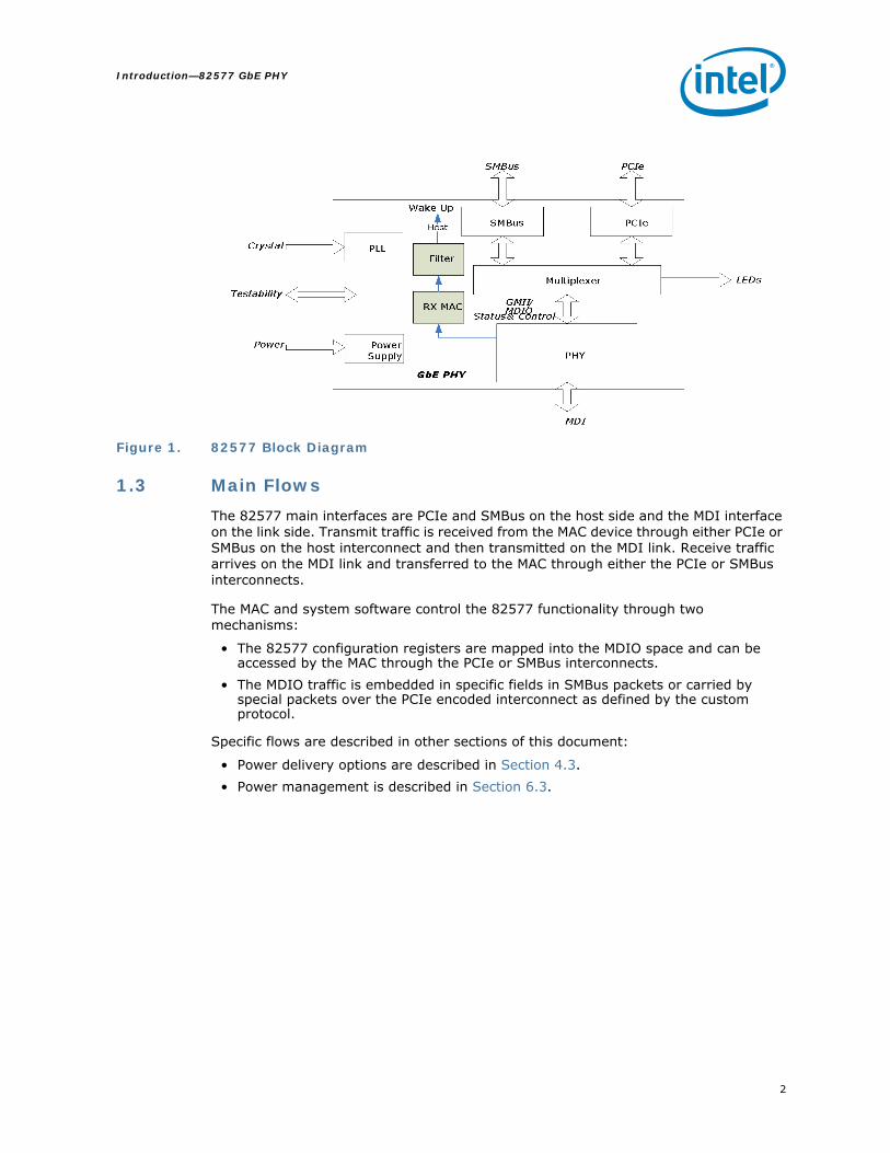
Figure 1. 82577 Block Diagram
1.3 Main FlowsThe 82577 main interfaces are PCIe and SMBus on the host side and the MDI interface on the link side. Transmit traffic is received from the MAC device through either PCIe or SMBus on the host interconnect and then transmitted on the MDI link. Receive traffic arrives on the MDI link and transferred to the MAC through either the PCIe or SMBus interconnects.
The MAC and system software control the 82577 functionality through two mechanisms:
• The 82577 configuration registers are mapped into the MDIO space and can be accessed by the MAC through the PCIe or SMBus interconnects.
• The MDIO traffic is embedded in specific fields in SMBus packets or carried by special packets over the PCIe encoded interconnect as defined by the custom protocol.
Specific flows are described in other sections of this document:
• Power delivery options are described in Section 4.3.• Power management is described in Section 6.3.

82577 GbE PHY—Introduction
3
1.4 References• Information Technology - Telecommunication & Information Exchange Between
Systems - LAN/MAN - Specific Requirements - Part 3: Carrier Sense Multiple Access with Collision Detection (CSMA/CD) Access Method and Physical Layer Specifications, IEEE Standard No.: 802.3-2002
• Intel® Ethernet Controllers Loopback Modes, Intel Corporation• SMBus specification revision 2.0.• Intel® 5 Series Express Chipset Family External Design Specification (Intel® 5
Series Express Chipset EDS), Intel Corporation• Intel® 5 Series Express Chipset External Datasheet Specification, Intel Corporation• Intel® 5 Series Express Chipset SPI Flash Programming Guide - Application Note,
Intel Corporation• Intel® 82577 Schematic and Layout Checklists, Intel Corporation• Intel® 82577 MDI Differential Trace and Power Loss Calculators, Intel Corporation
1.5 Product CodesTable 1 lists the product ordering codes for the 82577 GbE controller. Refer to the Intel® 82577 GbE PHY Specification Update for device ordering information.
Table 1. Product Ordering Codes
Device Market Segment Product Code
82577LM Corporate mobile and workstation WG82577LM
82577LC Consumer mobile WG82577LC

4
Introduction—82577 GbE PHY
1.6 Product Matrix
Note: The 82577 does not support server operating systems such as Windows Server* 2008 and Windows Server* 2003.

82577 GbE PHY—Interconnects
5
2.0 Interconnects
2.1 IntroductionThe 82577 implements two interconnects to the MAC:
• PCIe - A high-speed SerDes interface using PCIe electrical signaling at half speed while keeping the custom logical protocol for active state operation mode.
• System Management Bus (SMBus) – A very low speed connection for low power state mode for manageability communication only. At this low power state mode the Ethernet link speed is reduced to 10 Mb/s.
.
The 82577 automatically switches the in-band traffic between PCIe and SMBus based on the system power state.
2.2 PCIe-Based
Note: The 82577 PCIe interface is not PCIe compliant. It operates at half of the PCI Express* (PCIe*) Specification v1.1 (2.5 GT/s) speed. In this datasheet the term PCIe-based is interchangeable with PCIe. There is no design layout differences between normal PCIe and the 82577’s PCIe-based interface. Standard PCIe validation tools cannot be used to validate this interface.
2.2.1 PCIe Interface Signals
The signals used to connect between the MAC and the PHY in this mode are:
• Serial differential pair running at 1.25 Gb/s for Rx• Serial differential pair running at 1.25 Gb/s for Tx• 100 MHz differential clock input to the PHY running at 100 MHz• Power and clock good indication to the PHY PE_RST_N pin• Clock control through CLK_REQ_N pin
Table 2. 82577 Interconnect Modes
SystemPHY
SMBus PCIe
S0 and PHY Power Down Not used Idle
S0 and Idle or Link Disc Not used Idle
S0 and active Not used Active
Sx Active Power down
Sx and DMoff Active Power down

6
Interconnects—82577 GbE PHY
2.2.2 PCIe Operation and Channel Behavior
The 82577 only runs at 1250 Mb/s speed, which is 1/2 of the PCIe Specification v1.1, 2.5 Gb/s PCIe frequency. Each of the PCIe root ports in the Intel® 5 Series Express Chipset-integrated MAC have the ability to operate with the 82577. The port configuration is pre-loaded from the NVM. The selected port adjusts the transmitter to run at the 1.25 GHz rate and does not need to be PCIe compliant.
Packets transmitted and received over the PCIe interface are full Ethernet packets and not PCIe transaction/link/physical layer packets.
After the PCIe power-up sequence completes, each transmitter starts transmitting idle symbols and the receiver acquires synchronization as specified in 802.3z.
2.3 SMBus
Note: The 82577 SMBus must only be connected to SMLink0 in the Intel® 5 Series Express Chipset. No other device (like an external BMC) can be connected to SMLink0 when the 82577 is connected to the Intel® 5 Series Express Chipset SMLink0.
2.3.1 Overview
SMBus is used as an interface to pass traffic between the 82577 and the Intel® 5 Series Express Chipset when the system is in a low power state (Sx state). The interface is also used to enable the Intel® 5 Series Express Chipset to configure the 82577 as well as passing in-band information between them.
The SMBus uses two primary signals: SMB_CLK and SMB_DATA to communicate. Both of these signals float high with board-level pull-ups.
The SMBus specification has defined various types of message protocols composed of individual bytes. The message protocols supported by the 82577 are described in the relevant sections.
For more details about SMBus, see the SMBus specification.
2.3.1.1 SMBus Channel Behavior
The SMBus specification defines the maximum frequency of the SMBus as 100 KHz.
2.3.1.2 SMBus Addressing
The 82577’s address is assigned using SMBus ARP protocol. The default SMBus address is 0xC8.

82577 GbE PHY—Interconnects
7
2.3.1.3 Bus Timeouts
The 82577 can detect (as a master or a slave) an SMB_CLK timeout on the main SMBus. If the SMBus clock line is held low for 25 ms, the 82577 aborts the transaction.
As a slave, the 82577 detects the timeout and goes into an idle state. In idle, the slave releases the SMB_CLK and SMB_DATA lines. Any data that was received before the timeout might have been processed depending on the transaction.
As a master, the 82577 detects a timeout and issues a STOP on the SMBus at the next convenient opportunity and then brings the SMBus back to idle (releases SMB_CLK and SMB_DATA). Any master transaction that the 82577 detects a timeout on is aborted.
2.3.1.4 Bus Hangs
Although uncommon, SMBus bus hangs can happen in a system. The reason for the hang is typically an unexpected, asynchronous reset or noise coupled onto the SMBus. Slaves can contribute to SMBus hangs by not implementing the SMBus timeouts as specified in SMBus 2.0 specification. Masters or host masters can contribute to SMBus hangs by not detecting the failures and by not attempting to correct the bus hangs.
Because of the potential bus hang scenario, the 82577 has the capability of detecting a hung bus. If SMB_CLK or SMB_DATA are stuck low for more than 35 ms, the 82577 forces the bus to idle (both SMB_CLK and SMB_DATA set) if it is the cause of the bus hang.
2.3.1.5 Packet Error Code (PEC) Support
PEC is defined in the SMBus 2.0 specification. It is an extra byte at the end of the SMBus transaction, which is a CRC-8 calculated on all of the preceding bytes (not including ACKs, NACKs, STARTs, or STOPs) in the SMBus transaction. The polynomial for this CRC-8 is:
x8 + x2 + x + 1
The PEC calculation is reset when any of the following occurs:
• A STOP condition is detected on the host SMBus• An SMBus hang is detected on the host SMBus• The SMB_CLK is detected high for ~50 μs

8
Interconnects—82577 GbE PHY
2.3.1.6 SMBus ARP Functionality
The 82577 doesn’t support ARP protocol.
2.4 Transitions between SMBus and PCIe interfaces
2.4.1 Switching from SMBus to PCIe
Communication between the MAC and the 82577 is done through the SMBus each time the system is in a low power state (Sx); PE_RST_N signal is low. The MAC/PHY interface is needed to enable host wake up from the 82577.
Possible states for activity over the SMBus:
1. After power on (G3 to S5).2. On system standby (Sx).
While in this state, the SMBus is used to transfer traffic, configuration, control and status between the MAC and the 82577.
The switching from the SMBus to PCIe is done when the PE_RST_N signal is high.
• Any transmit/receive packet that is not completed when PE_RST_N is asserted is discarded.
• Any in-band message that was sent over the SMBus and was not acknowledged is re-transmitted over PCIe.
2.4.2 Switching from PCIe to SMBus
The communication between the MAC and the 82577 is done through PCIe each time the system is in active power state (S0); PE_RST_N signal is high. Switching the communication to SMBus is only needed to enable host wake up in low power states and is controlled by the Intel® 5 Series Express Chipset.
The switching from PCIe to SMBus is done when the PE_RST_N signal is low.
• Any transmit/receive packet that is not completed when PE_RST_N goes to 0b is discarded.
• Any in-band message that was sent over PCIe and was not acknowledged is re-transmitted over SMBus.
82577 GbE PHY—Interconnects
9
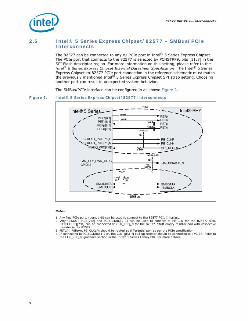
2.5 Intel® 5 Series Express Chipset/82577 – SMBus/PCIe InterconnectsThe 82577 can be connected to any x1 PCIe port in Intel® 5 Series Express Chipset. The PCIe port that connects to the 82577 is selected by PCHSTRP9, bits [11:8] in the SPI Flash descriptor region. For more information on this setting, please refer to the Intel® 5 Series Express Chipset External Datasheet Specification. The Intel® 5 Series Express Chipset-to-82577 PCIe port connection in the reference schematic must match the previously mentioned Intel® 5 Series Express Chipset SPI strap setting. Choosing another port can result in unexpected system behavior.
The SMBus/PCIe interface can be configured in as shown Figure 2.
Notes:
1. Any free PCIe ports (ports 1-8) can be used to connect to the 82577 PCIe Interface.2. Any CLKOUT_PCIE[7:0] and PCIECLKRQ[7:0] can be used to connect to PE_CLK for the 82577. Also,
PCIECLKRQ[7:0] can be connected to CLK_REQ_N for the 82577. Stuff empty resistor pad with respectiveresistor in the 82577.
3. PETp/n, PERp/n, PE_CLKp/n should be routed as differential pair as per the PCIe specification.4. If connecting to PCIECLKRQ[1:2]#, the CLK_REQ_N pull-up resistor should be connected to +V3.3S. Refer to the CLK_REQ_N guidance section in the Intel® 5 Series Family PDG for more details.
Figure 2. Intel® 5 Series Express Chipset/82577 Interconnects

10
Interconnects—82577 GbE PHY
Note: This page intentionally left blank.

82577 GbE PHY—Pin Interface
11
3.0 Pin Interface
3.1 Pin AssignmentThe 82577 is packaged in a 48-pin package, 6 x 6 mm with a 0.4 mm lead pitch. There are 48 pins on the periphery and a die pad (Exposed Pad*) for ground.
Note: Refer to the reference schematics for pin connection details. Contact your Intel representative for access.
3.1.1 Signal Type Definitions
Signal Type Definition
In Input is a standard input-only signal.
I A standard input-only signal.
Out (O) Totem pole output is a standard active driver.
T/s Tri-state is a bi-directional, tri-state input/output pin.
S/t/s
Sustained tri-state is an active low tri-state signal owned and driven by one and only one agent at a time. The agent that drives an s/t/s pin low must drive it high for at least one clock before letting it float. A new agent cannot start driving an s/t/s signal any sooner than one clock after the previous owner tri-states it.
O/d Open drain enables multiple devices to share as a wire-OR.
Analog Analog input/output signal.
A-in Analog input signal.
A-out Analog output signal.
B Input bias

12
Pin Interface—82577 GbE PHY
3.1.2 PCIe Interface Pins (8)
3.1.3 SMBus Interface Pins (2)
3.1.4 Miscellaneous Pins (3)
Pin Name Pin # Type Op Mode Name and Function
PE_RST_N 36 I Input PCIe reset.
PETpPETn
3839
A-out Output PCIe Tx.
PERpPERn
4142
A-in Input PCIe Rx.
PE_CLKPPE_CLKN
4445
A-in Input PCIe clock.
CLK_REQ_N 48 O/d Output Clock request. Connect to VCC3P3 through a 10 K pull-up resistor.
Pin Name Pin # Type Op Mode Name and Function
SMB_CLK 28 O/d BI-dir SMBus clock. Pull this signal up to 3.3 Vdc (auxiliary supply1) through a 2.2 K resistor (while in Sx mode).
SMB_DATA 31 O/d BI-dir SMBus data. Pull this signal up to 3.3 Vdc (auxiliary supply) through a 2.2 K resistor (while in Sx mode).
1. AUX power means the power rail is available in all power states including G3 to S5 transitions and Sx stateswith Wake on LAN (WoL) enabled.
Pin Name Pin # Type Op Mode Name and Function
RSVD1_VCC3P3 1 T/s Connect to VCC3P3 through a 5%, 3.01 K resistor.
RSVD2_VCC3P3 2 T/s Connect to VCC3P3 through a 5%, 3.01 K resistor.
LAN_DISABLE_N 3 IConnect to the LAN_PHY_PWR_CTRL/GPIO12 pin in the Intel® 5 Series Express Chipset.Note: When this pin is set to 0b, the 82577 is disabled.

82577 GbE PHY—Pin Interface
13
3.1.5 PHY Pins (14)
3.1.5.1 LEDs (3)
This table lists the functionality of the LED output pins. Refer to the Intel® 5 Series Family Platform Design Guide (PDG) for LED connection details.
3.1.5.2 Analog Pins (11)
Pin Name Pin # Type Op Mode Name and Function
LED0 26 O Output This signal is used for the programmable LED (LINK_LINK/ACTIVITY).
LED1 27 O Output This signal is used for the programmable LED (LINK_1000).
LED2 25 O Output This signal is used for the programmable LED (LINK_100).
Pin Name Pin# Type Op Mode Name and Function
MDI_PLUS[0]MDI_MINUS[0]
1314
Analog Bi-dir
Media Dependent Interface[0]1000BASE-T: In MDI configuration, MDI[0]+/- corresponds to BI_DA+/- and in MDI-X configuration MDI[0]+/- corresponds to BI_DB+/-.100BASE-TX: In MDI configuration, MDI[0]+/- is used for the transmit pair and in MDI-X configuration MDI[0]+/- is used for the receive pair.10BASE-T: In MDI configuration, MDI[0]+/- is used for the transmit pair and in MDI-X configuration MDI[0]+/- is used for the receive pair.
MDI_PLUS[1]MDI_MINUS[1]
1718
Analog Bi-dir
Media Dependent Interface[1]1000BASE-T: In MDI configuration, MDI[1]+/- corresponds to BI_DB+/- and in MDI-X configuration MDI[1]+/- corresponds to BI_DA+/-.100BASE-TX: In MDI configuration, MDI[1]+/- is used for the receive pair and in MDI-X configuration MDI[1]+/- is used for the transmit pair.10BASE-T: In MDI configuration, MDI[1]+/- is used for the receive pair and in MDI-X configuration MDI[1]+/- is used for the transmit pair.
MDI_PLUS[2]MDI_MINUS[2]MDI_PLUS[3]MDI_MINUS[3]
20212324
Analog Bi-dir
Media Dependent Interface[3:2]1000BASE-T: In MDI configuration, MDI[3:2]+/- corresponds to BI_DA+/- and in MDI-X configuration MDI[3:2]+/- corresponds to BI_DB+/-.100BASE-TX: Unused.10BASE-T: Unused.
XTAL_OUT 9 O Output crystal.
XTAL_IN 10 I Input crystal.
RBIAS 12 Analog Connect to ground through a 3.01 K +/-1%.

14
Pin Interface—82577 GbE PHY
3.1.6 Testability Pins (5)
Note: The 82577 uses the JTAG interface to support XOR files for manufacturing test. BSDL is not supported.
3.1.7 Power Pins (13)
3.1.8 LVR Power and Control Pins (3)
Pin Name Pin # Type Op Mode Name and Function
JTAG_TCK 35 In Input JTAG clock input.
JTAG_TDI 32InPU
Input JTAG TDI input.
JTAG_TDO 34 T/s Output JTAG TDO output.
JTAG_TMS 33InPU
Input JTAG TMS input.
TEST_EN 30 In Input Should be connected to ground through a 1 K resistor, when connected to logic 1b and test mode is enabled.
Pin Name Pin # Type Name and Function
VDD1P08, 11, 16, 22, 37, 40, 43,
46, 47Power
1.0 Vdc supply.Note: Can also be connected to the Intel® 5 Series Express Chipset Switching Voltage Regulator (SVR).
VDD3P3_OUT 4 Power Regulator output. Connect to GND through a 1 μF capacitor.
VDD3P3 15, 19, 29 Power Connect to GND through a 1 μF capacitor.
VDD3P3_IN 5 Power3.3 Vdc supply.Note: Make sure the 3.3 Vdc supply is connected to auxiliary power (available in all low power states).
Pin Name Pin # Type Name and Function
CTRL1P0 7 Analog Connect to the base of the PNP, if desired. Otherwise, leave as a No Connect.
VCT 6 Analog Leave as a no connect.
82577 GbE PHY—Package
15
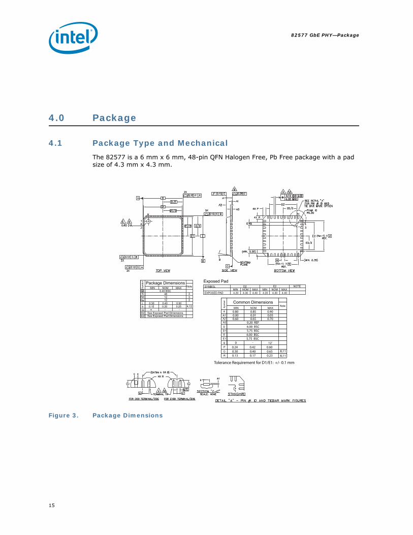
4.0 Package
4.1 Package Type and MechanicalThe 82577 is a 6 mm x 6 mm, 48-pin QFN Halogen Free, Pb Free package with a pad size of 4.3 mm x 4.3 mm.
Figure 3. Package Dimensions
-- - -
EXPOSED PAD
SYMBOL
Exposed PadD2 E2 NOTE
4.20 4.30 4.40 4.20 4.30 4.40MIN NOM MAX MIN NOM MAX
Common Dimensions
E2D2
See Exposed Pad DimensionsSee Exposed Pad Dimensions
QbL
Note
3
33
4,12
Sym
bol
e
NdN
Ne
MIN NOM MAX0.40 BSC
0.30 0.40 0.500.15 0.20 0.25
48
1212
Sym
bol
NoteMIN NOM MAX
0
AA1A2A3
DD1
E1E
R
_
P
O
0.80 0.85 0.900.00 0.01 0.050.60 0.65 0.70
0.20 REF6.00 BSC5.75 BSC6.00 BSC5.75 BSC
12’0 _
0.24 0.42 0.600.30 0.40 0.650.13 0.17 0.23 8,11
8,11
Tolerance Requirement for D1/E1: +/- 0.1 mm
Package Dimensions

16
Package—82577 GbE PHY
4.2 Package Electrical and Thermal CharacteristicsThe thermal resistance from junction to case, qJC, is 15.1 ×C/Watt.
The thermal resistance from junction to ambient, qJA, is as follows: 4-layer PCB, 85 degrees ambient.
No heat sink is required.
Air Flow (m/s) Maximum TJ qJA (×C/Watt)
0 119 34
1 118 33
2 116 31

82577 GbE PHY—Package
17
4.3 Power and Ground RequirementsThe 82577 requires two power supplies (3.3 Vdc and 1.0 Vdc). Figure 4 shows a typical power delivery configuration that can be implemented.
Note: Power delivery can be customized based on a specific OEM platform configuration.
Figure 4. 82577 Power Delivery Diagram
82577
CTRL1p0
R1 R2
R3
C1
C2
C4
1.0v
Q1 BCP69
C6 C5
43
22
R4
C3C7
C8 C9
6
3.3v4
7
3.3v15, 193.3v29
3.3VDD5
8,11,16,40
37,46,471.0v
3.01 Kohm 1%12
Center Tap
Magnetic
1uf
XTAL1
XTAL2
10
9
33pF
33pF
• C1, C2,C5 – X5R 10 uF 6.3V• C8, C9 – X5R 4.7uF 6.3V• C6, C3, C4 – 100 nF• R1 (4.99 Kohm)
R3 (0 ohm 0805) – Do Not PopulateR4 (0 ohm)C7 (0.01 uF) – Do Not Populate
• R2 (0 ohm 0805)
1.0V
1.0V
1.0V
1.0V
1uf
10pF
+3.3V LAN
X X
1.0V can be supplied from the Ibex Peak-M SVR
+3.3V LAN
– Do Not Populate
– Do Not Populate•••
No Connect

18
Package—82577 GbE PHY
4.4 Pinouts (Top View, Pins Down)
Figure 5. 82577 Pinouts
3839404142434445464748
8257748 Pin QFN
6 mm x 6 mm0.4 mm pin pitch
with Exposed Pad*
0P1
DD
V
N_Q
ER_
KLC
0P1
DD
V
0P1
DD
V
NKL
C_E
P
PKL
C_E
P
0P1
DD
V
nR
EP
pR
EP
0P1
DD
V
nTE
P
pTE
P
]0[S
ULP_I
DM
]3[S
UNI
M_ID
M
]3[S
ULP_I
DM
0P1
DD
V
]2[S
UNI
M_ID
M
]2[S
ULP_I
DM
3P3
DD
V
]1[S
UNI
M_ID
M
]1[S
ULP_I
DM
0P1
DD
V
3P3
DD
V
]0[S
UNI
M_ID
M
PE_RST_N
LED2
LED0
LED1
SMB_CLK
VDD3P3
TEST_EN
SMB_DATA
JTAG_TDIJTAG_TMS
JTAG_TDO
JTAG_TCKRSVD_VCC3P3
RBIAS
VDD1P0
XTAL_IN
XTAL_OUT
VDD1P0
CTRL_1P0
VCT
VDD3P3_INVDD3P3_OUT
LAN_DISABLE_N
363534333231302928
252627
123456789
101112
37
13 14 15 16 17 18 19 20 21 22 23 24
RSVD_VCC3P3
Pin 1Pin 49 - VSS_EPAD

82577 GbE PHY—Package
19
4.5 Ball Mapping
Pin Name Side Pin Number Pin Name Side Pin Number
RSVD_VCC3P3 Left 1 MDI_PLUS[0] Bottom 13
RSVD_VCC3P3 Left 2 MDI_MINUS[0] Bottom 14
LAN_DISABLE_N Left 3 VDD3P3 Bottom 15
VDD3P3_OUT Left 4 VDD1P0 Bottom 16
VDD3P3_IN Left 5 MDI_PLUS[1] Bottom 17
VCT Left 6 MDI_MINUS[1] Bottom 18
CTRL1P0 Left 7 VDD3P3 Bottom 19
VDD1P0 Left 8 MDI_PLUS[2] Bottom 20
XTAL_OUT Left 9 MDI_MINUS[2] Bottom 21
XTAL_IN Left 10 VDD1P0 Bottom 22
VDD1P0 Left 11 MDI_PLUS[3] Bottom 23
RBIAS Left 12 MDI_MINUS[3] Bottom 24
LED2 Right 25 VDD1P0 Top 37
LED0 Right 26 PETp Top 38
LED1 Right 27 PETn Top 39
SMB_CLK Right 28 VDD1P0 Top 40
VDD3P3 Right 29 PERp Top 41
TEST_EN Right 30 PERn Top 42
SMB_DATA Right 31 VDD1P0 Top 43
JTAG_TDI Right 32 PE_CLKP Top 44
JTAG_TMS Right 33 PE_CLKN Top 45
JTAG_TDO Right 34 VDD1P0 Top 46
JTAG_TCK Right 35 VDD1P0 Top 47
PE_RST_N Right 36 CLK_REQ_N Top 48
VSS_EPAD EPAD 49

20
Package—82577 GbE PHY
Note: This page intentionally left blank.

82577 GbE PHY—Initialization
21
5.0 Initialization
5.1 Power Up
Figure 6. Power-Up Sequence

22
Initialization—82577 GbE PHY
Table 3. Figure Notes
Note
1 Platform power ramps up (3.3 V dc/1.0 Vdc)
2 XTAL is stable after TXTAL sec.
3 Internal Power On Reset triggers TPOR after XTAL is stable. Strapping options are latched.
4 PCIe training if PE reset is de-asserted.
5 Wait for Intel® 5 Series Express Chipset SMBus address valid.
6 Send Link Status message.
7 MAC configures the 82577.
8 PHY goes through auto-negotiation to acquire link.
82577 GbE PHY—Initialization
23
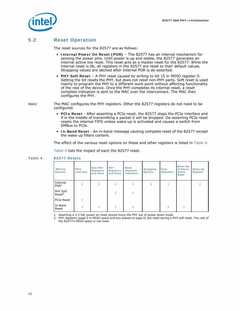
5.2 Reset OperationThe reset sources for the 82577 are as follows:
• Internal Power On Reset (POR) – The 82577 has an internal mechanism for sensing the power pins. Until power is up and stable, the 82577 generates an internal active low reset. This reset acts as a master reset for the 82577. While the internal reset is 0b, all registers in the 82577 are reset to their default values. Strapping values are latched after Internal POR is de-asserted.
• PHY Soft Reset – A PHY reset caused by writing to bit 15 in MDIO register 0. Setting the bit resets the PHY, but does not reset non-PHY parts. Soft reset is used mainly to program the PHY to a different work point without affecting functionality of the rest of the device. Once the PHY completes its internal reset, a reset complete indication is sent to the MAC over the interconnect. The MAC then configures the PHY.
Note: The MAC configures the PHY registers. Other the 82577 registers do not need to be configured.
• PCIe Reset - After asserting a PCIe reset, the 82577 stops the PCIe interface and if in the middle of transmitting a packet it will be dropped. De-asserting PCIe reset resets the internal FIFO unless wake-up is activated and causes a switch from SMBus to PCIe.
• In-Band Reset - An in-band message causing complete reset of the 82577 except the wake up filters content.
The effect of the various reset options on these and other registers is listed in Table 4.
Table 4 lists the impact of each the 82577 reset.
Table 4. 82577 Resets
Effects/ Sources
PCIe Interface
Non-PHY Registers and State
PHY Registers and State
Reset Complete Indication
Strapping Options
Fuse Registers
Move Out of Power Down Mode
Wake Up Register
Internal POR1
PHY Soft Reset2
PCIe Reset
In-Band Reset
1. Asserting a 3.3 Vdc power on reset should move the PHY out of power down mode.2. PHY registers (page 0 in MDIO space and any aliases to page 0) are reset during a PHY soft reset. The rest of
the 82577’s MDIO space is not reset.

24
Initialization—82577 GbE PHY
5.3 Timing Parameters
5.3.1 Timing Requirements
The 82577 requires the following start-up and power-state transitions.
5.3.2 Timing Guarantees
The 82577 guarantees the following start-up and power state transition related timing parameters.
Note: For platform power sequencing requirements for the Intel® 5 Series Express Chipset MAC, refer to the Intel® 5 Series Express Chipset EDS.
Table 5. Timing Requirements
Parameter Description Min. Max. Notes
Tr2init
Completing a PHY configuration following a reset complete indication.
0.5 s
Table 6. Timing Guarantees
Parameter Description Min Max Notes
TPHY_ResetReset de-assertion to PHY reset complete 10 ms PHY configuration should be delayed
until PHY completes it’s reset.
Tc2anCable connect at start of auto-negotiation 1.2 s 1.3 s Per 802.3 specification.

82577 GbE PHY—Power Management and Delivery
25
6.0 Power Management and Delivery
This section describes how power management is implemented in the 82577.
6.1 Power TargetsTable 7 lists the targets for device power for the 82577. Note that power is reduced according to link speed and link activity.
Note: Device power is the power dissipated by the 82577.

26
Power Management and Delivery—82577 GbE PHY
Table 7. 82577 Power Consumption Targets1
1. Measured power could be higher or lower based on measurement setup and PHY power delivery configuration.
System State Link State3.3 Vdc Current [mA]
1.05 Vdc Current [mA]
Device Power (mW)
Solution Power [mW] - Shared Intel® 5 Series Express Chipset SVR Solution2
2. SVR efficiency is assumed to be 80%.
Solution Power (mW) - BCP69 Solution
S0 (Max) 1000 Mb/s active @ 90 C [Ta] 94 326 653 738 1386
S0 (Typ)
1000 Mb/s active 94 302 627 707 1307
100 Mb/s active 59 138 340 376 650
10 Mb/s active 84 125 408 441 690
1000 Mb/s idle 83 231 516 577 1036
100 Mb/s idle 48 72 234 253 396
10 Mb/s idle 43 61 206 222 343
Cable disconnect 2 18 26 30 66
LAN disable 2 14 21 25 53
Sx WoL enabled
100 Mb/s - Wake on LAN (WoL) 47 73 232 251 396
10 Mb/s - WoL 43 61 206 222 343
WoL disabled
Disabled in BIOS3
3. Assumes the system is in the Moff state and SLP_LAN# is used to gate PHY power.
0 0 0 0 0
Disabled in driver 2 14 21 25 53

82577 GbE PHY—Power Management and Delivery
27
The following sections describe requirements in specific power states.
6.2 Power DeliveryThe 82577 operates from a 3.3 Vdc external power rail (see Figure 7).
6.2.1 1.0 Vdc Supply
The 1.0 Vdc rail can be supplied in one of two ways (see Figure 4):
• An external power supply not dependent on support from the 82577. For example, the Intel® 5 Series Express Chipset 1.05 Vdc SVR can be tied to the 1.0 Vdc PHY supply.
• A discrete LVR solution, where the base current of PNP power transistor is driven by the 82577, while the power transistor is placed externally.
6.3 Power Management
6.3.1 Global Power States
The 82577 transitions between power states based on a status packet received over the interconnect and based on the Ethernet link state. The following power states are defined:
• Power Up – Defined as the period from the time power is applied to the 82577 and until the 82577 powers up its PHY. The 82577 needs to consume less than 40 mA during this period.
• Active 10/100/1000 Mb/s – Ethernet link is established with a link partner at any of 10/100/1000 Mb/s speed. The 82577 is either transmitting/receiving data or is capable of doing so without delay (for example, no clock gating that requires lengthy wake).
• Idle 10/100/1000 Mb/s - Ethernet link is established with a link partner at any of 10/100/1000 Mb/s speed. The 82577 is not actively transmitting or receiving data and might enter a lower power state (for example, the custom interface can be in electrical idle).
• Cable Disconnect – The PHY identified that a cable is not connected. The 82577 signals the MAC that the link is down. The PHY might enter energy detect mode or the MAC might initiate a move into active power down mode (sD3).
• Power Down (LAN Disable) – Entry into power down is initiated by the MAC by setting the LAN_DISABLE_N pin to zero. The 82577 loses all functionality in this mode other than the ability to power up again.
•
6.3.1.1 Power Up
Defined as the period from the time power is applied to the 82577 and until the 82577 powers up its PHY. the 82577 should consume less than ~40 mA during this period. Following the 82577 PHY entering reset, the power-up sequence is considered done and the requirement is removed.

28
Power Management and Delivery—82577 GbE PHY
6.3.1.2 Cable Disconnect State
The 82577 enters a cable disconnect state if it detects a cable disconnect condition on the Ethernet link. Power is reduced during cable disconnect mode by several means:
• The PHY enters energy detect mode.• The PCIe link enters power down.
An exit from cable disconnect happens when the 82577 detects energy on the MDI link, and starts the following exit sequence:
• The 82577 signals the MAC that link energy was detected by clearing the Cable Disconnect bit in the PCIe or SMBus interface.
• The PHY waits until the auto-negotiation break link timer expires (Tc2an time) and then starts to advertise data on the line.
6.3.1.3 Power Down State
The 82577 enters a power-down state when the LAN_DISABLE_N pin is set to zero. Exiting this mode requires setting the LAN_DISABLE_N pin to a logic one.
Figure 7 shows the power-down sequence.
Figure 7. Power-Down Sequence
Note: If the LAN_DISABLE_N pin cannot be used, a power-down in-band can be used. When used, the power savings are lower since all logic cannot be turned off in this mode.
Table 8. Figure 7 Notes
Note Description
1 MAC sends an in-band power-down message through SMBus or PCIe or LAN_DISABLE_N pin set to zero.
2 Once the 82577 detects the power-down message or LAN_DISABLE_N transitions to a logic zero, the PHY enters a power-down state.
3 The PCIe link (if enabled) enters electrical idle state.
4 PCIe/SMBus exits a reset state and performs link initialization.
5 MAC configures the 82577 through the MDIO interface.
6 PHY goes through auto-negotiation to acquire link.

82577 GbE PHY—Power Management and Delivery
29
6.4 Power Saving FeaturesThis section provides information about the low power configurations for the 82577.
6.4.1 Intel® Auto Connect Battery Saver (ACBS)
Intel® Auto Connect Battery Saver for the 82577 is a hardware-only feature that automatically reduces the PHY to a lower power state when the power cable is disconnected. When the power cable is reconnected, it renegotiates the line speed following IEEE specifications for auto negotiation. By default, auto negotiation starts at 1 Gb/s, then 100 Mb/s full duplex/half duplex, then 10 Mb/s full duplex/half duplex.
Note: ACBS is only supported during auto negotiation. If link is forced, the 82577 does not enter ACBS mode.
82577 ACBS works in both S0 and Sx states. Since 82577 ACBS has no driver control, the feature is always enabled, allowing power savings by default.
Note: The crystal clock drivers are intermittently disabled when the network cable is unplugged and the 82577 is in ACBS mode.
6.4.2 Automatic Link Downshift
Automatic link downshift is a collection of power saving features that enable a link downshift from 1000 Mb/s to a lower speed to save power under different conditions like the AC cable plugged in, monitor idle, or entering Sx states.

30
Power Management and Delivery—82577 GbE PHY
6.4.2.1 Link Speed Battery Saver
Link speed battery saver is a power saving feature that negotiates to the lowest speed possible when the 82577 operates in battery mode to save power. When in AC mode, where performance is more important than power, it negotiates to the highest speed possible. The Windows NDIS drivers (Windows XP and later) monitor the AC-to-battery transition on the system to make the PHY negotiate to the lowest connection speed supported by the link partner (usually 10 Mb/s) when the power cable is unplugged (switches from AC to battery power). When the AC cable is plugged in, the speed negotiates back to the fastest LAN speed. This feature can be enabled/disabled directly from DMiX or through the advanced settings of the Window's driver.
When transferring packets at 1000/100 Mb/s speed, if there is an AC-to-battery mode transition, the speed renegotiates to the lower speed. Any packet that was in process is re-transmitted by the protocol layer. If the link partner is hard-set to only advertise a certain speed, then the driver negotiates to the advertised speed. Note that since the feature is driver based, it is available in S0 state only.
Link speed battery saver handles duplex mismatches/errors on link seamlessly by re-initiating auto negotiation while changing speed. Link speed battery saver also supports spanning tree protocol.
Note: Packets are re-transmitted for any protocol other than TCP as well.
6.4.2.2 System Idle Power Saver (SIPS)
SIPS is a software-based power saving feature that is enabled only with Microsoft* Windows* Vista* and Windows 7*. This feature is only supported in the S0 state and can be enabled/disabled using the advanced tab of the Windows driver or through DMiX. The power savings from this feature is dependent on the link speed of the 82577. Refer to Section 6.1 for the power dissipated in each link state.
SIPS is designed to save power in the 82577 by negotiating to the lowest possible link speed when both the network is idle and the monitor is turned off due to inactivity. The SIPS feature is activated based on both of the following conditions:
• The Windows* Vista*/Windows 7* NDIS driver receives notification from the operating system when the monitor is turned off due to non-activity.
• The LAN driver monitors the current network activity and determines that the network is idle.
Then, with both the monitor off and the network idle, the LAN negotiates to the lowest possible link speed supported by both the PHY and the link partner (typically 10 Mb/s). If the link partner is hard-set to only advertise a certain speed, then the LAN negotiates to the advertised speed. This link speed is maintained until the LAN driver receives notification from the operating system that the monitor is turned on, thus exiting SIPS and re-negotiating to the highest possible link speed supported by both the PHY and the link partner. If SIPS is exited when transferring packets, any packet that was being transferred is re-transmitted by the protocol layer after re-negotiation to the higher link speed.

82577 GbE PHY—Power Management and Delivery
31
6.4.2.3 Low Power Link Up (LPLU)
LPLU is a firmware/hardware-based feature that enables the designer to make the PHY negotiate to the lowest connection speed first and then to the next higher speed and so on. This power saving setting can be used when power is more important than performance.
When speed negotiation starts, the PHY tries to negotiate for a 10 Mb/s link, independent of speed advertisement. If link establishment fails, the PHY tries to negotiate with different speeds. It enables all speeds up to the lowest speed supported by the partner. For example, if the 82577 advertises 10 Mb/s only and the link partner supports 1000/100 Mb/s only, a 100 Mb/s link is established.
LPLU is controlled through the LPLU bit in the PHY Power Management register. The MAC sets and clears the bit according to hardware/software settings. The 82577 auto negotiates with the updated LPLU setting on the following auto-negotiation operation. The 82577 does not automatically auto-negotiate after a change in the LPLU value. LPLU is not dependent on whether the system is in Vac or Vdc mode. In S0 state, link speed battery saver overrides the LPLU functionality.
LPLU is enabled for non-D0a states by GbE NVM image word 0x17 (bit 10)
• 0b = LPLU is disabled. • 1b = LPLU is enabled in all non-D0a states.
LPLU power consumption depends on what speed it negotiates at. Section 6.1 includes all of the power numbers for the 82577 in the various speeds.

32
Power Management and Delivery—82577 GbE PHY
6.4.2.4 LAN Disable Recommendations
LAN_DISABLE_N needs to be connected to the GPIO12/LAN_PHY_PWR_CTRL output of the Intel® 5 Series Express Chipset. GPIO12 also needs to be configured using Intel® 5 Series Express Chipset soft straps as LAN_PHY_PWR_CTRL (bit [20] of PCHSTRP0 register - LAN_PHY_PWR_CTRL/GPIO12. Refer to the Intel® 5 Series Express Chipset Family External Design Specification (Intel® 5 Series Express Chipset EDS).

82577 GbE PHY—Device Functionality
33
7.0 Device Functionality
7.1 Tx FlowWhen packets are ready for transmission in the MAC it transfers them to the 82577 through the PCIe or the SMBus (depending on system state). The 82577 starts transmitting the arrived packet over the wire after it gathers eight bytes of data if the PCIe interface is active or after all packet data is received if it was transferred over the SMBus; however, this behavior has no dependency on link speed. The 82577 design is based on the assumption that the MAC has the full packet ready for transmission.
7.2 Rx FlowThe 82577 maintains a FIFO on the receive side in order not to lose packets when PCIe is active. In this case, the 82577 initiates recovery of the PCIe when a reception has started. If the link is at 1 Gb/s, the transmission of the packet over the PCIe bus starts immediately after recovery. if the link speed is lower, the 82577 starts the transmission after the entire packet is received.
7.3 Flow ControlFlow control as defined in 802.3x, as well as the specific operation of asymmetrical flow control defined by 802.3z, is supported in the MAC. Some of the flow control functionality has moved to the 82577. The following registers are duplicated to the 82577 for the implementation of flow control:
• Flow Control Address is: 0x01, 0x80, 0xC2, 0x00, 0x00, 0x01; where 0x01 is the first byte on the wire, 0x80 is the second, etc.
• Flow Control Type (FCT): a 16-bit field to indicate the flow control type.• Flow Control Transmit Timer Value (FCTTV): a 16-bit timer value to include in a
transmitted PAUSE frame.• Flow Control Refresh Threshold Value (FCRTV): a 16-bit PAUSE refresh threshold
value.
Flow control is implemented as a means of reducing the possibility of receive buffer overflows, which result in the dropping of received packets, and allows for local controlling of network congestion levels. This can be accomplished by sending an indication to a transmitting station of a nearly full receive buffer condition at a receiving station. The implementation of asymmetric flow control allows for one link partner to send flow control packets while being allowed to ignore their reception. For example, not required to respond to PAUSE frames.

34
Device Functionality—82577 GbE PHY
7.3.1 MAC Control Frames and Reception of Flow Control Packets
Three comparisons are used to determine the validity of a flow control frame:
1. A match on the six-byte multicast address for MAC control frames or to the station address of the device (Receive Address Register 0).
2. A match on the type field3. A comparison of the MAC Control Opcode field
The 802.3x standard defines the MAC control frame multicast address as 01-80-C2-00-00-01. The flow control packet’s Type field is checked to determine if it is a valid flow control packet: XON or XOFF. 802.3x reserves this as 0x8808. The final check for a valid PAUSE frame is the MAC Control Opcode field. At this time only the PAUSE control frame opcode is defined and has a value of 0x0001. Frame-based flow control differentiates XOFF from XON based on the value of the PAUSE Timer field. Non-zero values constitute XOFF frames while a value of zero constitutes an XON frame. Values in the Timer field are in units of slot time. A slot time is hardwired to 64 byte times.
Note: An XON frame signals cancelling the pause from being initiated by an XOFF frame (pause for zero slot times).
Figure 8. 802.3x MAC Control Frame Format
Where S is the start-of-packet delimiter and T is the first part of the end-of-packet delimiter for 802.3z encapsulation. The receiver is enabled to receive flow control frames if flow control is enabled via the RFCE bit in the Device Control (CTRL) register.
Note: Flow control capability must be negotiated between link partners via the auto-negotiation process. The auto-negotiation process might modify the value of these bits based on the resolved capability between the local device and the link partner.

82577 GbE PHY—Device Functionality
35
Once the 82577 has validated the reception of an XOFF, or PAUSE frame, it does the following:
• Initializes the pause timer based on the packet’s Pause Timer field• Disables packet transmission or schedules the disabling of transmission after the
current packet completes.• Sends an in-band status command with the TX OFF bit set.• Forward the XOFF or PAUSE frame to the MAC.
Resuming transmission might occur under the following conditions:
• Expiration of the PAUSE timer.• Reception of an XON frame (a frame with its PAUSE timer set to zero).1
Once the 82577 has validated the reception of an XON frame, it does the following:
• Enables packet transmission.• Sends an in-band status command with the Tx OFF bit cleared.• Forwards the XON frame to the MAC.
7.3.2 Transmitting PAUSE Frames
Transmitting PAUSE frames is done as a result of an In-Band Control command from the MAC. The MAC initiates an in-band message if it is enabled by software by writing a 1b to the TFCE bit in the Device Control register.
Note: Similar to receiving flow control packets previously mentioned, XOFF packets can be transmitted only if this configuration has been negotiated between the link partners via the auto-negotiation process. In other words, the setting of this bit indicates the desired configuration.
When the in-band message from the MAC is received, the 82577 sends a PAUSE frame with its Pause Timer field equal to FCTTV. Once the receive buffer fullness reaches the low water mark, the MAC sends an in-band message indicating to send an XON message (a PAUSE frame with a timer value of zero).
Note: Transmitting flow control frames should only be enabled in full-duplex mode per the IEEE 802.3 standard. Software should make sure that the transmission of flow control packets is disabled when the 82577 is operating in half-duplex mode.
7.4 Wake UpThe 82577 supports host wake up.
This mechanism uses in-band messages to wake the Intel® 5 Series Express Chipset from a sleep state. The host can enable host wake up from the 82577 by setting the Host_WU_Active bit. When this bit is set, after the host transitions to a low power state, the SMBus interface is still active and the wake up indication from the 82577 to the Intel® 5 Series Express Chipset would come in as an in-band message over the SMBus.
1. The XON frame is also forwarded to the MAC.

36
Device Functionality—82577 GbE PHY
Setting the 82577’s wake up:
1. Clear the Host_WU_Active bit (bit 4) in the Port General Configuration register (page 769, register 17) to enable wake up mode.
2. Set bit 2 (MACPD_enable) of the Port Control register (page 769, register 17) to enable the 82577 wake up capability and software accesses to page 800.
3. Set the Slave Access Enable bit (bit 2) in the Receive Control register (page 800, register 0) to enable access to the Flex Filter register, if setting those bits is needed in the next stage. The registers affected are:a. Flexible Filter Value Table LSB– FFVT_L (filters 01)b. Flexible Filter Value Table MSBs – FFVT_H (filters 23)c. Flexible Filter Value Table - FFVT_45 (filters 45)d. Flexible TCO Filter Value/Mask Table LSBs – FTFT_Le. Flexible TCO Filter Value/Mask Table MSBs – FTFT_H
4. Configure the 82577’s wake up registers per ACPI/APM wake up needs.5. Clear the Slave Access Enable bit (bit 2) in the Receive Control register (page 800,
register 0) to enable the flex filters.6. Set the Host_WU_Active bit (bit 4) in the Port General Configuration register (page
769, register 17) to activate the 82577’s wake up functionality.
Note: Once wake up is enabled, the 82577 stops responding to SMBus commands.
Host wake up:
1. When a WoL packet/event is detected, the 82577 sends an in-band message to the Intel® 5 Series Express Chipset indicating a host wake up.
2. The Intel® 5 Series Express Chipset wakes the host.3. The host should issue an PHY reset to the 82577 before clearing the Host_WU_Active bit.4. Host reads the Wake Up Status (WUS) register; wake up status from the 82577).
The 82577 keeps and forwards the wake up packet. When a wake up packet is identified, the wake up in-band message is sent and the host should clear the Host_WU_Active bit (bit 4) in the Port General Configuration register (page 769, register 17). As a result, the 82577 resumes transmitting the packet. Each time this bit is set and if a wake up in-band message has already sent, any new packets received does not overwrite the packet in the FIFO. The 82577 re-transmits the wake up in-band message after 50 ms if no change in the Host_WU_Active bit occurred.
7.4.1 Host Wake Up
The 82577 supports two types of wake up mechanisms:
• Advanced Power Management (APM) wake up• ACPI Power Management wake up

82577 GbE PHY—Device Functionality
37
7.4.1.1 Advanced Power Management Wake Up
Advanced Power Management Wakeup or APM Wakeup was previously known as Wake on LAN (WoL). The basic premise is to receive a broadcast or unicast packet with an explicit data pattern, and then to assert a signal to wake up the system or issue an in-band PM_PME message (if configured to).
At power up, if the 82577’s wake up functionality is enabled, the APM Enable bits from the NVM are written to the 82577 by the Intel® 5 Series Express Chipset to the APM Enable (APME) bits of the Wakeup Control (WUC) register. These bits control the enabling of APM wake up.
When APM wake up is enabled, the 82577 checks all incoming packets for Magic Packets. See Section 7.4.1.3.1.4 for a definition of Magic Packets.
To enable APM wake up, programmers should write a 1b to bit 10 in register 26 on page 0 PHY address 01, and then the station address to registers 27, 28, 29 at page 0 PHY address 01. The order is mandatory since registers RAL0[31:0] and RAH0[15:0] are updated with a corresponding value from registers 27, 28, 29, if the APM WoL Enable bit is set in register 26. The Address Valid bit (bit 31 in RAH0) is automatically set with a write to register 29, if the APM WoL Enable bit is set in register 26. The APM Enable bit (bit 0 in the WUC) is automatically set with a write to register 29, if the APM WoL Enable bit is set in register 26.
Once the 82577 receives a matching magic packet, it:
• Sets the Magic Packet Received bit in the WUS register.• Initiates the Intel® 5 Series Express Chipset wake up event through an in-band
message.
APM wake up is supported in all power states and only disabled if a subsequent NVM read results in the APM Wake Up bit being cleared or software explicitly writes a 0b to the APM Wake Up (APM) bit of the WUC register.
7.4.1.1.1 Link Status Change
When the LSCWO bit (bit 5 in the WUC register) is set, wake up is generated if all of the following conditions are met:
• APM wake up is enabled (APME bit is set in the WUC register)• The LSCWE bit (bit 4) is set in the WUC register• Link status change is detected
When the 82577 detects a link status change it:
• Sets the Link Status Changed (LNKC) bit (bit 0) in the WUS register.• Initiates the Intel® 5 Series Express Chipset wake up event.
When the LSCWO bit is set, wake up is never generated on link status change if either APM wake up is disabled or the LSCWE bit is cleared. In this case, the LNKC bit (bit 0) in the Wake up Filter Control (WUFC) register is read as zero, independent of the value written to it.

38
Device Functionality—82577 GbE PHY
7.4.1.2 ACPI Power Management Wake Up
The 82577 supports ACPI Power Management based wake ups and can generate system wake up events from three sources:
• Reception of a Magic Packet• Reception of a ACPI wake up packet• Detection of a link change of state
Activating ACPI Power Management wake up requires the following steps:
• Programming of the WUFC register to indicate the packets it needs to wake up and supplies the necessary data to the IPv4 Address Table (IP4AT) and the Flexible Filter Mask Table (FFMT), Flexible Filter Length Table (FFLT), and the Flexible Filter Value Table (FFVT). It can also set the Link Status Change Wake up Enable (LNKC) bit (bit 0) in the WUFC register to cause wake up when the link changes state.
• Setting bit 2 (MACPD_enable) of the Port Control register (page 769, register 17) to put the 82577 in wake up mode.
Once wake up is enabled, the 82577 monitors incoming packets by first filtering them according to its standard address filtering method and then by filtering them with all enabled wake up filters. If a packet passes both the standard address filtering and at least one of the enabled wake up filters, the 82577:
• Initiates a the Intel® 5 Series Express Chipset wake up event.• Sets one or more of the Received bits in the WUS register. Note that more than one
bit is set if a packet matches more than one filter.
If enabled, a link state change wake up causes similar results.
7.4.1.3 Wake Up Packets
The 82577 supports various wake up packets using two types of filters:
• Pre-defined filters• Flexible filters
Each of these filters are enabled if the corresponding bit in the WUFC register is set to 1b. If the wake up packet passes one of the manageability filters enabled in the Management Control (MANC) register, then system wake up also depends on the NoTCO bit (11) in the WUFC register being inactive.
7.4.1.3.1 Pre-Defined Filters
The following packets are supported by the 82577’s pre-defined filters:
• Directed Packet (including exact, multicast indexed, and broadcast)• Magic packet• IPv4 request packet• Directed IPv4 packet• Directed IPv6 packet• Flexible UDP/TCP and IP filters packets
Each of these filters are enabled if the corresponding bit in the WUFC register is set to 1b.

82577 GbE PHY—Device Functionality
39
The explanation of each filter includes a table showing which bytes at which offsets are compared to determine if the packet passes the filter. Note that both VLAN frames and LLC/Snap can increase the given offsets if they are present.
7.4.1.3.1.1 Directed Exact Packet
The 82577 generates a wake up event after receiving any packet whose destination address matches one of the seven valid programmed receive addresses if the Directed Exact Wake Up Enable bit (bit 2) is set in the WUFC register.
7.4.1.3.1.2 Directed Multicast Packet
For multicast packets, the upper bits of the incoming packet’s destination address indexes a bit vector and the Multicast Table Array indicates whether to accept the packet. If the Directed Multicast Wake Up Enable bit (bit 3) is set in the WUFC register and the indexed bit in the vector is one, the 82577 generates a wake up event. The exact bits used in the comparison are programmed by software in the Multicast Offset field (bits 4:3) of the RCTL register.
7.4.1.3.1.3 Broadcast
If the Broadcast Wake Up Enable bit (bit 4) in the WUFC register is set, the 82577 generates a wake up event when it receives a broadcast packet.
Offset # of Bytes Field Value Action Comment
0 6 Destination Address Compare Match any pre-programmed address as defined in the receive address
Offset # of Bytes Field Value Action Comment
0 6 Destination Address Compare See previous paragraph.
Offset # of Bytes Field Value Action Comment
0 6 Destination Address FF*6 Compare

40
Device Functionality—82577 GbE PHY
7.4.1.3.1.4 Magic Packet
Magic packets are defined as follows:
— Magic Packet Technology Details - Once the 82577 has been put into Magic Packet mode, it scans all incoming frames addressed to the node for a specific data sequence, which indicates to the MAC that this is a Magic Packet frame. A Magic Packet frame must also meet the basic requirements for the LAN technology chosen, such as Source address, Destination Address (which might be the receiving station’s IEEE address or a Multicast address that includes the Broadcast address) and CRC. The specific data sequence consists of 16 duplications of the IEEE address of this node with no breaks or interruptions. This sequence can be located anywhere within the packet, but must be preceded by a synchronization stream. The synchronization stream enables the scanning state machine to be much simpler. The synchronization stream is defined as 6 bytes of 0xFF. The device also accepts a Broadcast frame, as long as the 16 duplications of the IEEE address match the address of the system that needs to wake up.
The 82577 expects the destination address to either:
1. Be the broadcast address (FF.FF.FF.FF.FF.FF)2. Match the value in Receive Address (RAH0/RAL0) register 0. This is initially loaded
from the NVM but can be changed by the software device driver.3. Match any other address filtering enabled by the software device driver.
If the packet destination address met one of the three criteria previously listed, the 82577 searches for 16 repetitions of the same destination address in the packet's data field. Those 16 repetitions must be preceded by (in the data field) at least 6 bytes of 0xFF, which act as a synchronization stream. If the destination address is NOT the broadcast address (FF.FF.FF.FF.FF.FF), the 82577 assumes that the first non-0xFF byte following at least 6 0xFF bytes is the first byte of the possible matching destination address. If the 96 bytes following the last 0xFF are 16 repetitions of the destination address, the 82577 accepts the packet as a valid wake up Magic Packet. Note that this definition precludes the first byte of the destination address from being 0xFF.
A Magic Packet’s destination address must match the address filtering enabled in the configuration registers with the exception that broadcast packets are considered to match even if the Broadcast Accept bit (bit 5) of the RCTL register is 0b. If APM wake up is enabled in the NVM, the 82577 starts up with the RAH0/RAL0 register 0 loaded from the NVM. This enables the 82577 to accept packets with the matching IEEE address before the software device driver comes up.
Offset # of Bytes Field Value Action Comment
0 6 Destination Address Compare
MAC Header – processed by main address filter
6 6 Source Address Skip
12 4 Possible VLAN Tag Skip
12 8 Possible Len/LLC/SNAP Header Skip
12 4 Type Skip
Any 6 Synchronizing Stream FF*6+ Compare
any+6 96 16 copies of Node Address A*16 Compare Compared to RAH0/RAL0 register

82577 GbE PHY—Device Functionality
41
7.4.1.3.1.5 IPv4 Request Packet
Three IPv4 addresses are supported, which are programmed in the IPv4 Address Table (IP4AT). A successfully matched packet must contain a broadcast MAC address, a protocol type of 0x0806, and one of the four programmed IPv4 addresses.
Offset # of Bytes Field Value Action Comment
0 6 Destination Address Compare
MAC Header – processed by main address filter
6 6 Source Address Skip
12 4 Possible VLAN Tag Skip
12 8 Possible Len/LLC/SNAP Header Skip
12 2 Type 0x0806 Compare
14 2 Hardware Type 0x0001 Compare
16 2 Protocol Type 0x0800 Compare
18 1 Hardware Size 0x06 Compare
19 1 Protocol Address Length 0x04 Compare
20 2 Operation 0x0001 Compare
22 6 Sender Hardware Address - Ignore
28 4 Sender IP Address - Ignore
32 6 Target Hardware Address - Ignore
38 4 Target IP Address IP4AT Compare Might match any of four values in IP4AT
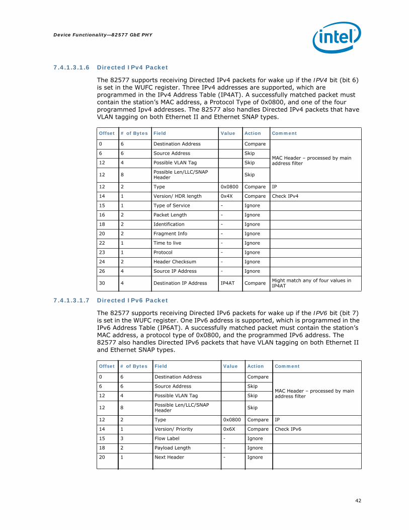
42
Device Functionality—82577 GbE PHY
7.4.1.3.1.6 Directed IPv4 Packet
The 82577 supports receiving Directed IPv4 packets for wake up if the IPV4 bit (bit 6) is set in the WUFC register. Three IPv4 addresses are supported, which are programmed in the IPv4 Address Table (IP4AT). A successfully matched packet must contain the station’s MAC address, a Protocol Type of 0x0800, and one of the four programmed Ipv4 addresses. The 82577 also handles Directed IPv4 packets that have VLAN tagging on both Ethernet II and Ethernet SNAP types.
7.4.1.3.1.7 Directed IPv6 Packet
The 82577 supports receiving Directed IPv6 packets for wake up if the IPV6 bit (bit 7) is set in the WUFC register. One IPv6 address is supported, which is programmed in the IPv6 Address Table (IP6AT). A successfully matched packet must contain the station’s MAC address, a protocol type of 0x0800, and the programmed IPv6 address. The 82577 also handles Directed IPv6 packets that have VLAN tagging on both Ethernet II and Ethernet SNAP types.
Offset # of Bytes Field Value Action Comment
0 6 Destination Address Compare
MAC Header – processed by main address filter
6 6 Source Address Skip
12 4 Possible VLAN Tag Skip
12 8 Possible Len/LLC/SNAP Header Skip
12 2 Type 0x0800 Compare IP
14 1 Version/ HDR length 0x4X Compare Check IPv4
15 1 Type of Service - Ignore
16 2 Packet Length - Ignore
18 2 Identification - Ignore
20 2 Fragment Info - Ignore
22 1 Time to live - Ignore
23 1 Protocol - Ignore
24 2 Header Checksum - Ignore
26 4 Source IP Address - Ignore
30 4 Destination IP Address IP4AT Compare Might match any of four values in IP4AT
Offset # of Bytes Field Value Action Comment
0 6 Destination Address Compare
MAC Header – processed by main address filter
6 6 Source Address Skip
12 4 Possible VLAN Tag Skip
12 8 Possible Len/LLC/SNAP Header Skip
12 2 Type 0x0800 Compare IP
14 1 Version/ Priority 0x6X Compare Check IPv6
15 3 Flow Label - Ignore
18 2 Payload Length - Ignore
20 1 Next Header - Ignore

82577 GbE PHY—Device Functionality
43
7.4.1.3.2 Flexible Filter
The 82577 supports a total of six flexible filters. Each filter can be configured to recognize any arbitrary pattern within the first 128 bytes of the packet. To configure the flexible filter, software programs the mask values into the Flexible Filter Mask Table (FFMT) and the required values into the Flexible Filter Value Table (FFVT), and the minimum packet length into the Flexible Filter Length Table (FFLT). These contain separate values for each filter. Software must also enable the filter in the WUFC register, and enable the overall wake up functionality must be enabled by setting PME_En in the Power Management Control Status Register (PMCSR) or the WUC register.
Once enabled, the flexible filters scan incoming packets for a match. If the filter encounters any byte in the packet where the mask bit is one and the byte doesn’t match the byte programmed in the Flexible Filter Value Table (FFVT) then the filter fails that packet. If the filter reaches the required length without failing the packet, it passes the packet and generates a wake up event. It ignores any mask bits set to one beyond the required length.
Note: The following packets are listed for reference purposes only. The flexible filter could be used to filter these packets.
7.4.1.3.2.1 IPX Diagnostic Responder Request Packet
An IPX Diagnostic Responder Request packet must contain a valid MAC address, a protocol type of 0x8137, and an IPX diagnostic socket of 0x0456. It might include LLC/SNAP Headers and VLAN Tags. Since filtering this packet relies on the flexible filters, which use offsets specified by the operating system directly, the operating system must account for the extra offset LLC/SNAP Headers and VLAN tags.
7.4.1.3.2.2 Directed IPX Packet
A valid Directed IPX packet contain the station’s MAC address, a protocol type of 0x8137, and an IPX node address that equals to the station’s MAC address. It might include LLC/SNAP Headers and VLAN Tags. Since filtering this packet relies on the flexible filters, which use offsets specified by the operating system directly, the operating system must account for the extra offset LLC/SNAP Headers and VLAN tags.
Offset # of Bytes Field Value Action Comment
21 1 Hop Limit - Ignore
22 16 Source IP Address - Ignore
38 16 Destination IP Address IP6AT Compare Match value in IP6AT
Offset # of Bytes Field Value Action Comment
0 6 Destination Address Compare
6 6 Source Address Skip
12 4 Possible VLAN Tag Skip
12 8 Possible Len/LLC/SNAP Header Skip
12 2 Type 0x8137 Compare IPX
14 16 Some IPX Information - Ignore
30 2 IPX Diagnostic Socket 0x0456 Compare

44
Device Functionality—82577 GbE PHY
7.4.1.3.2.3 IPv6 Neighbor Solicitation Message Filter
In IPv6, a Neighbor Solicitation Message packet (type 135) is used for address resolution. A flexible filter can be used to check for a Neighborhood Solicitation Message packet (type 135).
Note: The fields checked for detection of a Neighbor Solicitation Message packet (type 135) are type, code and addresses.
7.4.2 Accessing The 82577’s Wake Up Register Using MDIC
When software needs to configure the wake up state (either read or write to these registers) the MDIO page should be set to 800 (for host accesses) until the page is not changed to a different value wake up register access is enabled. Refer to Section 8.10.1 for more details.
After the page is set to the wake up page, the Address field is no longer translated as reg_addr (register address) but as an instruction. If the given address is in [0..15] range meaning PHY registers, the functionality remains unchanged.
There are two valid instructions:
Offset # of Bytes Field Value Action Comment
0 6 Destination Address Compare
MAC Header – processed by main address filter
6 6 Source Address Skip
12 4 Possible VLAN Tag Skip
12 8 Possible Len/LLC/SNAP Header Skip
12 2 Type 0x8137 Compare IPX
14 10 Some IPX Information - Ignore
24 6 IPX Node Address Receive Address 0 Compare Must match Receive
Address 0
Instruction Address Description
Address set 0x11 Wake up space address is set for either reading or writing.
Data cycle 0x12 Wake up space accesses read or write cycle.
82577 GbE PHY—Device Functionality
45
7.5 PHY LoopbackPHY loopback is supported in the 82577. Software or firmware should set the 82577 to the loopback mode (via the MDIC register) writing to the PHY Loopback Control register (address 19). The MAC must be in forced link and in full duplex mode for PHY loopback to operate. The following bits must be configured to enable PHY loopback:
CTRL.FRCDPLX = 1b: // force duplex mode by the MAC
CTRL.FD = 1b: // Set full-duplex mode

46
Device Functionality—82577 GbE PHY
Note: This page intentionally left blank.

82577 GbE PHY—Programmer’s Visible State
47
8.0 Programmer’s Visible State
8.1 Terminology
This document names registers as follows.
• By register number— Registers 0-15 are independent of the page and can be designated by their
register number.— When a register number is used for registers 16-21, or 23-28, it refers to the
register in page 0.— Register 31 in PHY address 01, is the page register itself and doesn’t belong to
any page. It is always written as register 31.• By page and register number
— This can be written out as page x, register y, but is often abbreviated x.y• By name
— Most functional registers also have a name.
Shorthand Description
R/W Read/Write. A register with this attribute can be read and written. If written since reset, the value read reflects the value written.
R/W S Read/Write Status. A register with this attribute can be read and written. This bit represents status of some sort, so the value read might not reflect the value written.
RO Read Only. If a register is read only, writes to this register have no effect.
WO Write Only. Reading this register might not return a meaningful value.
R/WC Read/Write Clear. A register bit with this attribute can be read and written. However, a write of 1b clears (sets to 0b) the corresponding bit and a write of 0b has no effect.
R/W SC Read/Write Self Clearing. When written to 1b the bit causes an action to be initiated. Once the action is complete the bit return to 0b.
RO/LHRead Only, Latch High. The bit records an event or the occurrence of a condition to be recorded. When the event occurs the bit is set to 1b. After the bit is read, it returns to 0b unless the event is still occurring.
RO/LL Read Only, Latch Low. The bit records an event. When the event occurs the bit is set to 0b. After the bit is read, it reflects the current status.
RO/SC Read Only, Self Clear. Writes to this register have no effect. Reading the register clears (set to 0b) the corresponding bits.
RW0 Ignore Read, Write Zero. The bit is a reserved bit. Any values read should be ignored. When writing to this bit always write as 0b.
RWPIgnore Read, Write Preserving. This bit is a reserved bit. Any values read should be ignored. However, they must be saved. When writing the register the value read out must be written back. (There are currently no bits that have this definition.)

48
Programmer’s Visible State—82577 GbE PHY
Register bits are designated by a dot followed by a number after the register address. Thus, bit 4.16.2 is page 4, register 16 and bit 2. Multi-bit fields follow the MSB, colon, LSB convention and so bits 4.16.5:4 is page 4, register 16, bits 5:4. All fields in a register have a name.
Register bits with default values marked with an asterisk * are loaded by the MAC during the 82577 power up and following reset. Other fields in the same 16-bit register must be loaded with their default values.
8.2 MDIO AccessAfter PHY reset, a delay of 10 ms is required before any register access using MDIO. Access using MDIO should be done only when bit 10 in page 769 register 16 is set.
8.3 AddressingAddressing is based on the IEEE 802.3 MII Management Interface specification defined in clause 22 of 802.3, particularly section 22.2.4.
The 82577 registers are spread over two PHY addresses 01, 02, where general registers are located under PHY address 01 and the PHY specific registers are at PHY address 02. The IEEE specification allows five bits for the register access. Registers 0 to 15 are defined by the specification, while registers 16 to 31 are left available to the vendor. The PHY implements many registers for diagnostic purposes. In addition, the 82577 contains registers controlling the custom interface as well as other the 82577 functions. The total number of registers implemented far exceeds the 16 registers available to the vendor. When this occurs, a common technique is to use paging. The 82577 registers in PHY address 01, are divided into pages. Each page has 32 registers. Registers 0-15 are identical in all the pages and are the IEEE defined registers. Register 31 is the page register in all pages of PHY address 01. All other registers are page specific.
In order to read or write a register, software should define the appropriate PHY address. For PHY address 01, in order to access registers other than 0-15, software should first set the page register to map to the appropriate page. Software can then read or write any register in that page. Setting the page is done by writing page_num x 32 to Register 31. This is because only the 11 MSB’s of register 31 are used for defining the page. During write to the page register, the five LSB’s are ignored.
In pages 800 and 801, the register address space is more than 32. See section 8.9 for a description of registers addressing in these pages.
Accessing more than 32 registers in PHY address 02, is done without using pages. Instead, two registers from register address 16 to 31 are used as Address Offset port and Data port for extended set of registers. See section 8.5 for details about these registers.

82577 GbE PHY—Programmer’s Visible State
49
8.4 Address MapTable 9. Address Map
PHY Address Page Register Name Table #
02 Any 0 Control Table 10
02 Any 1 Status Table 11
02 Any 2 PHY Identifier 1 Table 12
02 Any 3 PHY Identifier 2 Table 13
02 Any 4 Auto-Negotiation Advertisement Table 14
02 Any 5 Auto-Negotiation Link Partner Ability Table 15
02 Any 6 Auto-Negotiation Expansion Table 16
02 Any 7 Auto-Negotiation Next Page Transmit Table 17
02 Any 8 Link Partner Next Page Table 18
02 Any 9 1000BASE-T Control Table 19
02 Any 10 1000BASE-T Status Table 20
02 Any 14:11 Reserved
02 Any 15 Extended Status Table 21
02 0 17:16 Reserved
02 0 18 PHY Control 2 Table 22
02 0 19 Loopback Control Table 26
02 0 20 Rx Error Counter Table 28
02 0 21 Reserved Table 29
02 0 22 PHY Configuration Table 30
02 0 23 PHY Control Table 31
02 0 24 Interrupt Mask Table 32
02 0 25 Interrupt Status Table 42
02 0 26 PHY Status Table 43
02 0 27 LED Control 1 Table 45
02 0 28 LED Control 2 Table 46
02 0 29 LED Control 3 Table 64
02 0 30 Diagnostics Control (Linking Disabled) Table 65
02 0 31 Diagnostics Status Table 66
Page 769 – Port Control Registers
01 769 16 Custom Mode Control Table 41
01 769 17 Port General Configuration Table 42
01 769 21 Power Management Control Table 43
01 769 25 Rate Adaptation Control Table 45
01 769 27 Flow Control Transmit Timer Value Table 46
Page 778 – Statistics Registers
01 778 16 - 17 Single Collision Count Table 47
01 778 18 - 19 Excessive Collisions Count Table 48
01 778 20 - 21 Multiple Collisions Count Table 49

50
Programmer’s Visible State—82577 GbE PHY
01 778 23 - 24 Late Collision Count Table 50
01 778 25 - 26 Collision Count Table 51
01 778 27 - 28 Defer Count Table 52
01 778 29 - 30 Transmit with No CRS - TNCRS Table 53
PCIe Registers
01 770 16 PCIe FIFOs Control/Status Table 54
01 770 17 PCIe Power Management Control Table 55
01 770 18 In-Band Control Table 56
01 770 20 PCIe Diagnostics Table 57
01 770 21 Timeouts Table 58
01 770 23 PCIe K-State Minimum Duration Timeout Table 59
General Registers
01 776 19 82577 Capability Register Table 60
01 0 25 OEM Bits Table 61
01 0 26 SMBus Address Table 62
01 0 27-28 Shadow Register for RAL0[31:0]. Table 63
01 0 29 Shadow Register for RAH0[15:0]. Table 64
01 0 30 LED Configuration Table 65
Page 800 - Wake Up Registers
01 800 0 Receive Control Register Table 66
01 800 1 Wake Up Control Register Table 67
01 800 2 Wake Up Filter Control Register Table 68
01 800 3 Wake Up Status Register Table 69
01 800 16 Receive Address Low 0 Table 70
01 800 18 Receive Address High 0 Table 71
01 800 44 - 45 Shared Receive Address Low 0 Table 72
01 800 46 - 47 Shared Receive Address High 0 Table 73
01 800 58 - 59 Shared Receive Address High 3 Table 74
01 800 64 IP Address Valid – IPAV Table 75
01 800 82 - 83 IPv4 Address Table – IP4AT 0 Table 76
01 800 88 - 89 IPv6 Address Table – IP6AT 0 Table 77
01 800 128 - 191 Multicast Table Array – MTA[31:0] Table 78
01 800 256 + 2*n (n = 0 - 127) Flexible Filter Value Table LSB– FFVT_01 Table 79
01 800 257 + 2*n (n = 0 - 127) Flexible Filter Value Table MSB – FFVT_23 Table 80
01 800 512 + 2*n (n = 0 - 127) Flexible Filter Value Table – FFVT_45 Table 81
01 800 768 + n (n = 0 - 127) Flexible Filter Mask Table – FFMT Table 82
01 800 896 + n (n = 0 - 3) Flexible Filter Length Table – FFLT03 Table 83
01 800 904 + n (n=0…1) Flexible Filter Length Table – FFLT45 Table 84
Table 9. Address Map

82577 GbE PHY—Programmer’s Visible State
51
8.5 PHY Registers (Page 0)
Table 10. Control Register - Address 0
Bits Field Type Default Description
15 Reset R/W, SC 0b
Writing a 1b to this bit causes immediate PHY reset. Once the operation completes, this bit clears to 0b automatically1b = PHY reset.0b = Normal operation.
14 Loopback R/W 0b
This is the master enable for digital and analog loopback as defined by the IEEE standard. The exact type of loopback is determined by the Loopback Control register (19). See section 7.5 for more details).1b = Enables loopback.0b = Disables loopback.
13 Speed Select (LSB) R/W X
The speed selection address 0 (bits 13 and 6) can be used to configure the link manually. Setting these bits has no effect unless address 0 (bit 12) is cleared.11b = Reserved.10b = 1000 Mb/s.01b = 100 Mb/s.00b = 10 Mb/s.
12Auto-Negotiation Enable
R/W 1b
When this bit is cleared, the link configuration is determined manually.1b = Enables auto-negotiation process.0b = Disables auto-negotiation process.
11 Power Down R/W 0b1b = Power down.0b = Normal operation.
10 Isolate R/W 0b
Setting this bit isolates the PHY from the MII or GMII interfaces.1b = Isolates the PHY from MII.0b = Normal operation.
9 Restart Auto-Negotiation R/W,SC 0b
1b = Restarts auto-negotiation process.0b = Normal operation.
8 Duplex Mode R/W X
This bit might be used to configure the link manually. Setting this bit has no effect unless address 0 (bit 12) is cleared.1b = Full-duplex.0b = Half-duplex.
7 Collision Test R/W 0bEnables IEEE 22.2.4.1.9 collision test.1b = Enable collision test.0b = Disable collision test.
6Speed Selection (MSB)
R/W X See description in bit 13.
5:0 Reserved RO Always 0x0 Reserved, always set to 0x0.

52
Programmer’s Visible State—82577 GbE PHY
Table 11. Status Register - Address 1
Bits Field Type Default Description
15 100BASE-T4 RO 0b100BASE-T4. This protocol is not supported. This register bit is always set to 0b. 0b = Not 100BASE-T4 capable.
14 100BASE-TX Full-Duplex RO X
1b = 100BASE-TX full duplex capable.0b = Not 100BASE-TX full duplex capable.
13 100BASE-TX Half-Duplex RO X
1b = 100BASE-TX half duplex capable.0b = Not 100BASE-TX half duplex capable.
12 10 Mb/s Full- Duplex RO X
1b = 10BASE-T full duplex capable.0b = Not 10BASE-T full duplex capable.
11 10 Mb/s Half-Duplex RO X
1b = 10BASE-T half duplex capable.0b = Not 10BASE-T half duplex capable.
10 100BASE-T2 Full-Duplex RO 0b Not able to perform 100BASE-T2.
9 100BASE-T2 Half-Duplex RO 0b Not able to perform 100BASE-T2.
8 Extended Status RO 1b Extended status information in the register Extended Status (0xF).
7 Reserved RO 0b Must always be set to 0b.
6 MF Preamble Suppression RO 1b 1b = PHY accepts management frames with preamble
suppressed.
5Auto- Negotiation Complete
RO 0bThis bit is set after auto-negotiation completes.1b = Auto-negotiation process complete.0b = Auto-negotiation process not complete.
4 Remote Fault RO,LH 0b
This bit indicates that a remote fault has been detected. Once set, it remains set until it is cleared by reading register 1 via the management interface or by PHY reset.1b = Remote fault condition detected.0b = Remote fault condition not detected.
3Auto-Negotiation Ability
RO 1b1b = PHY able to perform auto-negotiation.0b = PHY not able to perform auto-negotiation.
2 Link Status RO,LL 0b
This bit indicates that a valid link has been established. Once cleared, due to link failure, this bit remains cleared until register 1 is read via the management interface.1b = Link is up.0b = Link is down.
1 Jabber Detect RO,LH 0b1b = Jabber condition detected.0 = Jabber condition not detected.
0 Extended Capability RO 1b
Indicates that the PHY provides an extended set of capabilities that might be accessed through the extended register set. For a PHY that incorporates a GMII/RGMII, the extended register set consists of all management registers except registers 0, 1, and 15.1b = Extended register capabilities.

82577 GbE PHY—Programmer’s Visible State
53
Any write to the Auto-Negotiation Advertisement register, prior to auto-negotiation completion, is followed by a restart of auto-negotiation. Also note that this register is not updated following auto-negotiation.
Table 12. PHY Identifier Register 1 - Address 2
Bits Field Type Default Description
15:0Unique Identifier Bits 18:3
RO 0x0154Organizationally Unique Identifier (OUI), bits [18:3].Note: The OUI is 00-AA-00.
Table 13. PHY Identifier Register 2 - Address 3
Bits Field Type Default Description
15:10 PHY Identifier Bits 24:19 RO 000000b
OUI, bits [24:19].Note: The OUI is 00-AA-00.
9:4 Model Number RO 000101b The value is part of the PHY identifier and represents the device model number.
3:0 Revision Number RO 0x3 The value is part of the PHY identifier and represents the
device revision number.
Table 14. Auto-Negotiation Advertisement Register -Address 4
Bits Field Type Default Description
15 Next Page R/W 0b1b = Advertises next page ability supported.0b = Advertises next page ability not supported.
14 Reserved RO Always 0b Must be 0b.
13 Remote Fault R/W 0b1b = Advertises remote fault detected.0b = Advertises no remote fault detected.
12 Reserved R/W 0b Reserved
11 Asymmetric Pause R/W X1b = Advertises asymmetric pause ability.0b = Advertises no asymmetric pause ability.
10 Pause Capable R/W X1b = Capable of full duplex pause operation.0b = Not capable of pause operation.
9 100BASE-T4 Capability R/W 0b
The PHY does not support 100BASE-T4. The default value of this register bit is 0b.1b = 100BASE-T4 capable.0b = Not 100BASE-T4 capable.
8 100BASE-TX Full-Duplex Capable R/W X
1b = 100BASE-TX full duplex capable.0b = Not 100BASE-TX full duplex capable.
7 100BASE-TX Half-Duplex Capable R/W X
1b = 100BASE-TX half duplex capable.0b = Not 100BASE-TX half duplex capable.
6 10BASE-TX Full-Duplex Capable R/W X
1b = 10BASE-TX full duplex capable.0b = Not 10BASE-TX full duplex capable.
5 10BASE-TX Half-Duplex Capable R/W X
1b = 10BASE-TX half duplex capable.0b = Not 10BASE-TX half duplex capable.
4:0 Selector Field R/W 00001b 00001b = IEEE 802.3 CSMA/CD.

54
Programmer’s Visible State—82577 GbE PHY
Table 15. Auto-Negotiation Link Partner Ability Register - Address 5
Bits Field Type Default Description
15 Next Page RO 0b1b = Link partner has next page ability.0b = Link partner does not have next page ability.
14 Acknowledge RO 0b1b = Link partner has received link code word.0b = Link partner has not received link code word.
13 Remote Fault RO 0b1b = Link partner has detected remote fault.0b = Link partner has not detected remote fault.
12 Reserved RO 0b Reserved.
11 Asymmetric Pause RO 0b1b = Link partner requests asymmetric pause.0b = Link partner does not request asymmetric pause.
10 Pause Capable RO 0b1b = Link partner is capable of full duplex pause operation.0b = Link partner is not capable of pause operation.
9 100BASE-T4 Capability RO 0b
1b = Link partner is 100BASE-T4 capable.0b = Link partner is not 100BASE-T4 capable.
8 100BASE-TX Full-Duplex Capability RO 0b
1b = Link partner is 100BASE-TX full-duplex capable.0b = Link partner is not 100BASE-TX full-duplex capable.
7 100BASE-TX Half-Duplex Capability RO 0b
1b = Link partner is 100BASE-TX half-duplex capable.0b = Link partner is not 100BASE-TX half-duplex capable.
6 10BASE-T Full-Duplex Capability RO 0b
1b = Link partner is 10BASE-T full-duplex capable.0b = Link partner is not 10BASE-T full-duplex capable.
5 10BASE-T Half-Duplex Capability RO 0b
1b = Link partner is 10BASE-T half-duplex capable.0b = Link partner is not 10BASE-T half-duplex capable.
4:0 Protocol Selector Field RO 0x00 Link partner protocol selector field.
Table 16. Auto-Negotiation Expansion Register - Address 6
Bits Field Type Default Description
15:5 Reserved RO 0x00 Reserved, must be set to 0x00.
4 Parallel Detection Fault RO,LH 0b
1b = Parallel link fault detected. 0b = Parallel link fault not detected.
3 Link Partner Next Page Ability RO 0b
1b = Link partner has next page capability.0b = Link partner does not have next page capability.
2 Next Page Capability RO, LH 1b
1b = Local device has next page capability.0b = Local device does not have next page capability.
1 Page Received RO, LH 0b
1b = A new page has been received from a link partner.0b = A new page has not been received from a link partner.
0 Link Partner Auto- Negotiation Ability RO 0b
1b = Link partner has auto-negotiation capability.0b = Link partner does not have auto-negotiation capability.
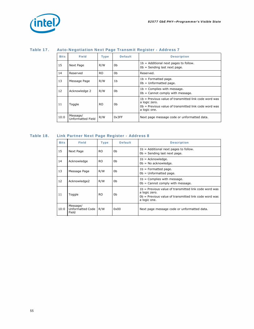
82577 GbE PHY—Programmer’s Visible State
55
Table 17. Auto-Negotiation Next Page Transmit Register - Address 7
Bits Field Type Default Description
15 Next Page R/W 0b1b = Additional next pages to follow.0b = Sending last next page.
14 Reserved RO 0b Reserved.
13 Message Page R/W 1b1b = Formatted page.0b = Unformatted page.
12 Acknowledge 2 R/W 0b1b = Complies with message.0b = Cannot comply with message.
11 Toggle RO 0b
1b = Previous value of transmitted link code word was a logic zero.0b = Previous value of transmitted link code word was a logic one.
10:0 Message/ Unformatted Field R/W 0x3FF Next page message code or unformatted data.
Table 18. Link Partner Next Page Register - Address 8
Bits Field Type Default Description
15 Next Page RO 0b1b = Additional next pages to follow.0b = Sending last next page.
14 Acknowledge RO 0b1b = Acknowledge.0b = No acknowledge.
13 Message Page R/W 0b1b = Formatted page.0b = Unformatted page.
12 Acknowledge2 R/W 0b1b = Complies with message.0b = Cannot comply with message.
11 Toggle RO 0b
1b = Previous value of transmitted link code word was a logic zero.0b = Previous value of transmitted link code word was a logic one.
10:0Message/Unformatted Code Field
R/W 0x00 Next page message code or unformatted data.

56
Programmer’s Visible State—82577 GbE PHY
Note: Logically, bits 12:8 can be regarded as an extension of the Technology Ability field in register 4.
Table 19. 1000BASE-T Control PHY Register - Address 9
Bits Field Type Default Description
15:13 Test Mode R/W 000b
000b = Normal mode.001b = Test Mode 1 - Transmit waveform test.010b = Test Mode 2 - Master transmit jitter test.011b = Test Mode 3 - Slave transmit jitter test.100b = Test Mode 4 - Transmit distortion test.101b, 110b, 111b = Reserved.
12
Master/Slave Manual Configuration Enable
R/W 0b1b = Enables master/slave configuration.0b = Automatic master/slave configuration.
11Master/Slave Configuration Value
R/W 0b
Setting this bit has no effect unless address 9, bit 12 is set.1b = Configures PHY as a master.0b = Configures PHY as a salve.
10 Port Type R/W X1b = Multi-port device (prefer master).0b = Single port device (prefer slave).
9Advertise 1000BASE-T Full-Duplex Capability
R/W X1b = Advertises 1000BASE-T full-duplex capability.0b = Advertises no 1000BASE-T full-duplex capability.
8
Advertise 1000BASE-T Half-Duplex Capability
R/W X1b = Advertises 1000BASE-T half-duplex capability.0b = Advertises no 1000BASE-T half-duplex capability.
7:0 Reserved RO 0x00 Set these bits to 0x00.
Table 20. 1000BASE-T Status Register - Address 10
Bits Field Type Default Description
15Master/Slave Configuration Fault
RO,LH, SC 0b
Once set, this bit remains set until cleared by the following actions:• Read of register 10 via the management interface.• Reset.• Auto-negotiation completed.• Auto-negotiation enabled.
1b = Master/slave configuration fault detected.0b = No master/slave configuration fault detected.
14Master/Slave Configuration Resolution
RO 0bThis bit is not valid when bit 15 is set.1b = Local PHY resolved to master.0b = Local PHY resolved to slave.
13 Local Receiver Status RO 0b
1b = Local receiver is correct.0b = Local receiver is incorrect.
12 Remote Receiver Status RO 0b
1b = Remote receiver is correct.0b = Remote receiver is incorrect.
11
Link Partner 1000BASE-T Full-Duplex Capability
RO 0b
1b = Link partner 1000BASE-T full-duplex capable.0b = Link partner not 1000BASE-T full-duplex capable.Note: Logically, bits 11:10 might be regarded as an extension of the Technology Ability field in register 5.
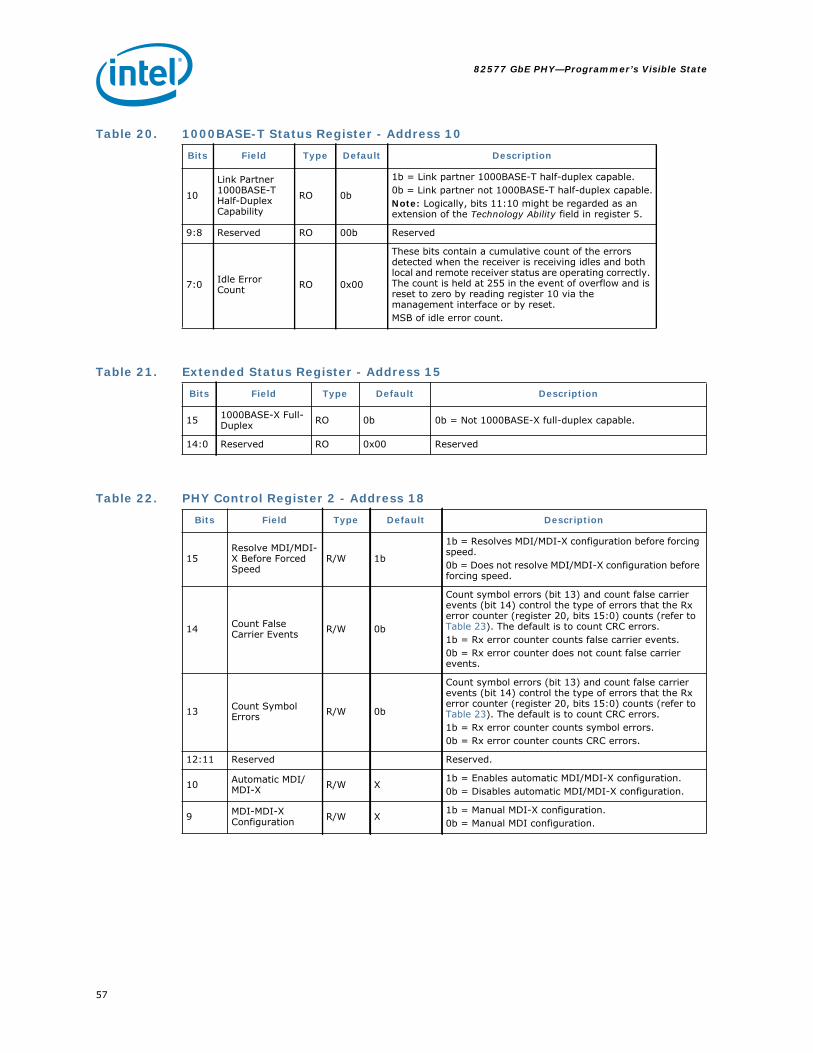
82577 GbE PHY—Programmer’s Visible State
57
10
Link Partner 1000BASE-T Half-Duplex Capability
RO 0b
1b = Link partner 1000BASE-T half-duplex capable.0b = Link partner not 1000BASE-T half-duplex capable.Note: Logically, bits 11:10 might be regarded as an extension of the Technology Ability field in register 5.
9:8 Reserved RO 00b Reserved
7:0 Idle Error Count RO 0x00
These bits contain a cumulative count of the errors detected when the receiver is receiving idles and both local and remote receiver status are operating correctly. The count is held at 255 in the event of overflow and is reset to zero by reading register 10 via the management interface or by reset.MSB of idle error count.
Table 20. 1000BASE-T Status Register - Address 10
Bits Field Type Default Description
Table 21. Extended Status Register - Address 15
Bits Field Type Default Description
15 1000BASE-X Full-Duplex RO 0b 0b = Not 1000BASE-X full-duplex capable.
14:0 Reserved RO 0x00 Reserved
Table 22. PHY Control Register 2 - Address 18
Bits Field Type Default Description
15Resolve MDI/MDI-X Before Forced Speed
R/W 1b
1b = Resolves MDI/MDI-X configuration before forcing speed.0b = Does not resolve MDI/MDI-X configuration before forcing speed.
14 Count False Carrier Events R/W 0b
Count symbol errors (bit 13) and count false carrier events (bit 14) control the type of errors that the Rx error counter (register 20, bits 15:0) counts (refer to Table 23). The default is to count CRC errors.1b = Rx error counter counts false carrier events.0b = Rx error counter does not count false carrier events.
13 Count Symbol Errors R/W 0b
Count symbol errors (bit 13) and count false carrier events (bit 14) control the type of errors that the Rx error counter (register 20, bits 15:0) counts (refer to Table 23). The default is to count CRC errors.1b = Rx error counter counts symbol errors.0b = Rx error counter counts CRC errors.
12:11 Reserved Reserved.
10 Automatic MDI/MDI-X R/W X
1b = Enables automatic MDI/MDI-X configuration.0b = Disables automatic MDI/MDI-X configuration.
9 MDI-MDI-X Configuration R/W X
1b = Manual MDI-X configuration.0b = Manual MDI configuration.

58
Programmer’s Visible State—82577 GbE PHY
8:3 Reserved Reserved.
2 Enable Diagnostics R/W
This bit enables PHY diagnostics, which include IP phone detection and TDR cable diagnostics. It is not recommended to enable this bit in normal operation (when the link is active). This bit does not need to be set for link analysis cable diagnostics.1b = Enables diagnostics.0b = Disables diagnostics.
1:0 Reserved Reserved.
Table 22. PHY Control Register 2 - Address 18
Bits Field Type Default Description

82577 GbE PHY—Programmer’s Visible State
59
Table 23. Rx Error Counter Characteristics
Bit 9 of the PHY Control register manually sets the MDI/MDI-X configuration if automatic MDI-X is disabled (refer to Table 24).
Table 24. MDI/MDI-X Configuration Parameters
The mapping of the transmitter and receiver to pins for MDI and MDI-X configuration for 10BASE-T, 100BASE-TX, and 1000BASE-T is listed in Table 25. Note that even in manual MDI/MDI-X configuration, the PHY automatically detects and corrects for C and D pair swaps.
Table 25. MDI/MDI-X Pin Mapping
Count False Carrier Events
Count Symbol Errors Rx Error Counter
1 1 Counts symbol errors and false carrier events.
1 0 Counts CRC errors and false carrier events.
0 1 Counts symbol errors.
0 0 Counts CRC errors.
Automatic MDI/MDI-X
MDI/MDI-X Configuration MDI/MDI-X Mode
1 X Automatic MDI/MDI-X detection.
0 0 MDI configuration (NIC/DTE).
0 1 MDI-X configuration (switch).
Pin MDI Pin Mapping MDI-X Pin Mapping
10BASE-T 100BASE-TX 1000BASE-T 10BASE-T 100BASE-TX 1000BASE-T
TRD[0]+/- Tx +/- Tx +/-Tx A+/-Rx B+/-
Rx +/- Rx +/-Tx B+/-Rx A+/-
TRD[1]+/- Rx +/- Rx +/-Tx B+/-Rx A+/-
Tx +/- Tx +/-Tx A+/-Rx B+/-
TRD[2]+/-Tx C+/-Rx D+/-
Tx D+/-Rx C+/-
TRD[3]+/-Tx D+/-Rx C+/-
Tx C+/-Rx D+/-
Table 26. Loopback Control Register - Address 191
Bits Field Type Default Description
15 MII R/W 1b1b = MII loopback selected.0b = MII loopback not selected.
14:13 Reserved Reserved
12 All Digital R/W 0b1b = All digital loopback enabled.0b = All digital loopback disabled.

60
Programmer’s Visible State—82577 GbE PHY
8.5.1 Loopback Mode Settings1
Table 27 lists how the loopback bit (Register 0, bit 14) and the Link Enable bit (Register 23, bit 13) should be set for each loopback mode. It also indicates whether the loopback mode sets the Link Status bit and when the PHY is ready to receive data.
Table 27. Loopback Bit (Register 0, Bit 14) Settings for Loopback Mode
11 Reserved Reserved
10 Line Driver R/W 0b1b = Line driver loopback enabled.0b = Line driver loopback disabled.
9 Remote R/W 0b1b = Remote loopback enabled.0b = Remote loopback disabled.
8 Reserved R/W Reserved
7 External Cable R/W 0b1b = External cable loopback enabled.0b = External cable loopback disabled.
6 Tx Suppression R/W 1b1b = Suppress Tx during all digital loopback.0b = Do not suppress Tx during all digital loopback.
5:1 Reserved Reserved
0 Force Link Status R/W 1b
This bit can be used to force link status operational during MII loopback. In MII loopback, the link status bit is not set unless force link status is used. In all other loopback mode, the link status bit is set when the link comes up.1b = Forces link status operational in MII loopback.0b = Forces link status not operational in MII loopback.
1. See section 7.5 for more details.
1. See section 7.5 for more details.
Table 26. Loopback Control Register - Address 191
Bits Field Type Default Description
Loopback Register 0, Bit 14 = 1b
Register 26, Bit 6 (Link Status Set) PHY Ready for Data
MII Yes Register 19, bit 0 After a few ms
All Digital Yes Yes Link Status
Line Driver Yes Yes Link Status
Ext Cable No Yes Link Status
Remote No Yes Never
Table 28. Rx Error Counter Register - Address 20
Bits Field Type Default Description
15:0 Rx Error Counter RO, SC 0x0016-bit Rx error counter.Note: Refer to register 18, bits 13 and 14 for error type descriptions.

82577 GbE PHY—Programmer’s Visible State
61
Table 29. Management Interface (MI) Register - Address 21
Bits Field Type Default Description
15:4 Reserved Reserved
3 Energy Detect Power Down Enable R/W X
1b = Enables energy detect power down.0b = Disables energy detect power down.
2:0 Reserved Reserved
Table 30. PHY Configuration Register - Address 22
Bits Field Type Default Description
15 CRS Transmit Enable R/W 0b1b = Enables Carrier Sense Indication (CRS) on transmit in half-duplex mode.0b = Disables CRS on transmit.
14 Reserved R/W 1b Reserved
13:12 Transmit FIFO Depth (1000BASE-T) R/W 01b
00b = +/-8.01b = +/-16.10b = +/-24.11b = +/-32.
11:10 Automatic Speed Downshift Mode R/W GX
If automatic downshift is enabled and the PHY fails to auto-negotiate at 1000BASE-T, the PHY falls back to attempt connection at 100BASE-TX and, subsequently, 10BASE-T. This cycle repeats. If the link is broken at any speed, the PHY restarts this process by re-attempting connection at the highest possible speed (1000BASE-T).00b = Automatic speed downshift disabled.01b = 10BASE-T downshift enabled.10b = 100BASE-TX downshift enabled.11b = 100BASE-TX and 10BASE-T enabled.
9:8 Reserved Reserved
7 Alternate Next Page R/W 0b
1b = Enables manual control of 1000BASE-T next pages only.0b = Normal operation of 1000BASE-T next page exchange.
6 Group MDIO Mode Enable R/W 0b
1b = Enables group MDIO mode.0b = Disables group MDIO mode.
5 Transmit Clock Enable R/W 0b
When this bit is set, the transmit test clock is available on pin TX_TCLK.1b = Enables output of mixer clock (transmit clock in 1000BASE-T).0b = Disables output.
4:0 Reserved 0x0 Reserved

62
Programmer’s Visible State—82577 GbE PHY
Table 31. PHY Control Register - Address 23
Bits Field Type Default Description
15 Reserved RO 0b Reserved
14 Reserved R/W, SC 0b Reserved
13 LNK_EN (Link Enable) R/W X
If LNK_EN is set, the PHY attempts to bring up a link with a remote partner and monitors the MDI for link pulses. If LNK_EN is cleared, the PHY takes down any active link, goes into standby, and does not respond to link pulses from a remote link partner. In standby, IP phone detect and TDR functions are available.1b = Enables linking.0b = Disables linking.
12:10Automatic Speed Downshift Attempts Before Downshift
R/W X
000b = 1.001b = 2.010b = 3.011b = 4.100b = 5.101b = 6.110b = 7.111b = 8.
9:8 Reserved Reserved
7 Link Partner Detected RO, LH 0b
When linking is disabled, the PHY automatically monitors for the appearance of a link partner and sets this bit if detected. Linking is disabled when LNK_EN is cleared (bit 13 = 0b).1b = Link partner detected.0b = Link partner not detected.
6 Jabber (10BASE-T) R/W 0b1b = Disables jabber.0b = Normal operation.
5 SQE (10BASE-T) R/W 0b1b = Enables heartbeat.0b = Disables heartbeat.
4 TP_LOOPBACK (10BASE-T) R/W 1b
1b = Disables TP loopback during half duplex.0b = Normal operation.
3:2 10BASE-T Preamble Length R/W 1b
00b = 10BASE-T preamble length of zero bits.01b = 10BASE-T preamble length of eight bits.1xb = Reserved.
1:0 Reserved Reserved

82577 GbE PHY—Programmer’s Visible State
63
Table 32. Interrupt Mask Register - Address 24
Bits Field Type Default Description
15:11 Reserved Reserved.
10 TDR/IP Phone R/W 0b1b = Interrupt enabled.0b = Interrupt disabled.
9 MDIO Sync Lost R/W 0b1b = Interrupt enabled.0b = Interrupt disabled.
8 Auto-Negotiation Status Change R/W 0b
1b = Interrupt enabled.0b = Interrupt disabled.
7 CRC Errors R/W 0b1b = Interrupt enabled.0b = Interrupt disabled.
6 Next Page Received R/W 0b1b = Interrupt enabled.0b = Interrupt disabled.
5 Error Count Full R/W 0b1b = Interrupt enabled.0b = Interrupt disabled.
4 FIFO Overflow/Underflow R/W 0b
1b = Interrupt enabled.0b = Interrupt disabled.
3 Receive Status Change R/W 0b1b = Interrupt enabled.0b = Interrupt disabled.
2 Link Status Change R/W 0b1b = Interrupt enabled.0b = Interrupt disabled.
1 Automatic Speed Downshift R/W 0b
1b = Interrupt enabled.0b = Interrupt disabled.
0 MDINT_N Enable R/W 0b1b = MDINT_N enabled.1
0b = MDINT_N disabled.
1. MDINT_N is asserted (active low) if MII interrupt pending = 1b.

64
Programmer’s Visible State—82577 GbE PHY
Table 33. Interrupt Status Register - Address 25
Bits Field Type Default Description
15:11 Reserved Reserved.
10 TDR/IP Phone RO, LH 0b1b = Event completed.0b = Event has not completed.
9 MDIO Sync Lost RO, LH 0b
If the management frame preamble is suppressed (MF preamble suppression, Register 0, bit 6), it is possible for the PHY to lose synchronization if there is a glitch at the interface. The PHY can recover if a single frame with a preamble is sent to the PHY. The MDIO sync lost interrupt can be used to detect loss of synchronization and, thus, enable recovery.1b = Event has occurred.0b = Event has not occurred.
8 Auto-Negotiation Status Change RO, LH 0b
1b = Event has occurred.0b = Event has not occurred.
7 CRC Errors RO, LH 0b1b = Event has occurred.0b = Event has not occurred.
6 Next Page Received RO, LH 0b1b = Event has occurred.0b = Event has not occurred.
5 Error Count Full RO, LH 0b1b = Event has occurred.0b = Event has not occurred.
4 FIFO Overflow/Underflow RO, LH 0b
1b = Event has occurred.0b = Event has not occurred.
3 Receive Status Change RO, LH 0b1b = Event has occurred.0b = Event has not occurred.
2 Link Status Change RO, LH 0b1b = Event has occurred.0b = Event has not occurred.
1 Automatic Speed Downshift RO, LH 0b
1b = Event has occurred.0b = Event has not occurred.
0 MII Interrupt Pending RO, LH 0b
An event has occurred and the corresponding interrupt mask bit is enabled (set to 1b).1b = Interrupt pending.0b = No interrupt pending.

82577 GbE PHY—Programmer’s Visible State
65
Table 34. PHY Status Register - Address 26
Bits Field Type Default Description
15 PHY in Standby RO 0b
This bit indicates that the PHY is in standby mode and is ready to perform IP phone detection or TDR cable diagnostics. The PHY enters standby mode when LNK_EN is cleared (Register 23, bit 13 = 0b) and exits standby mode and attempts to auto-negotiate a link when LNK-EN is set (Register 23, bit 13 = 1b).1b = PHY in standby mode.0b = PHY not in standby mode.
14:13 Auto-Negotiation Fault Status RO 00b
11b = Reserved.10b = Master/slave auto-negotiation fault.01b = Parallel detect auto-negotiation fault.00b = No auto-negotiation fault.
12 Auto-Negotiation Status RO 0b
1b = Auto-negotiation complete.0b = Auto-negotiation not complete.
11 Pair Swap on Pairs A and B RO 0b
1b = Pairs A and B swapped.0b = Pairs A and B not swapped.
10 Polarity Status RO 1b1b = Polarity inverted (10BASE-T only).0b = Polarity normal (10BASE-T only).
9:8 Speed Status RO 11b
11b = Undetermined.10b = 1000BASE-T.01b = 100BASE-TX.00b = 10BASE-T.
7 Duplex Status RO 0b1b = Full duplex.0b = Half duplex.
6 Link Status RO 0b1b = Link up.0b = Link down.
5 Transmit Status RO 0b1b = PHY transmitting a packet.0b = PHY not transmitting a packet.
4 Receive Status RO 0b1b = PHY receiving a packet.0b = PHY not receiving a packet.
3 Collision Status RO 0b1b = Collision occurring.0b = Collision not occurring.
2 Auto-Negotiation Enabled RO 0b
1b = Both partners have auto-negotiation enabled.0b = Both partners do not have auto-negotiation enabled.
1 Link Partner Advertised PAUSE RO 0b
1b = Link partner advertised PAUSE.0b = Link partner did not advertise PAUSE.
0 Link Partner Advertised Asymmetric PAUSE RO 0b
1b = Link partner advertised asymmetric PAUSE.0b = Link partner did not advertise asymmetric PAUSE.

66
Programmer’s Visible State—82577 GbE PHY
Table 35. LED Control Register 1 - Address 27
Bits Field Type Default Description
15 Two-Color Mode LED_100/LED_10 R/W 0b
If two-color mode is enabled for pair LED_LNK/ACT and LED_1000, the signal output for LED_LNK/ACT is equal to LED_LNK/ACT and LED_1000. When LED_LNK/ACT and LED_1000 are not mutually exclusive (such as duplex and collision), this mode can simplify the external circuitry because it ensures either LED_LNK/ACT and LED_1000 is on, and not both at the same time. The same rule applies to pair LED_100 and LED_10.1b = Two-color mode for LED_100 and LED_10.0b = Normal mode for LED_100 and LED_10.
14Two-Color Mode LED_LNK/ACT/LED_1000
R/W 0b
If two-color mode is enabled for pair LED_LNK/ACT and LED_1000, the signal output for LED_LNK/ACT is equal to LED_LNK/ACT and LED_1000. When LED_LNK/ACT and LED_1000 are not mutually exclusive (such as duplex and collision), this mode can simplify the external circuitry because it ensures either LED_LNK/ACT and LED_1000 is on, and not both at the same time. The same rule applies to pair LED_100 and LED_10.1b = Two-color mode for LED_LNK/ACT and LED_1000.0b = Normal mode for LED_LNK/ACT and LED_1000.
13 LED_10 Extended Modes R/W X
The LED function is programmed using this bit and Register 28.1b = Extended modes for LED_10.0b = Standard modes for LED_10.
12 LED_100 Extended Modes R/W X
The LED function is programmed using this bit and Register 28.1b = Extended modes for LED_100.0b = Standard modes for LED_100.
11 LED_1000 Extended Modes R/W X
The LED function is programmed using this bit and Register 28.1b = Extended modes for LED_1000.0b = Standard modes for LED_1000.
10 LED_LNK/ACT Extended Modes R/W X
The LED function is programmed using this bit and Register 28.1b = Extended modes for LED_LNK/ACT.0b = Standard modes for LED_LNK/ACT.
9:8 Reserved Reserved
7:4 LED Blink Pattern Pause R/W 0x0 LED blink pattern pause cycles.

82577 GbE PHY—Programmer’s Visible State
67
3:2 LED Pause Duration R/W 00b
The pulse duration for the setting, Register 27, bits 3:2 = 11b, can be programmed in the range 0 ms to 2 s, in steps of 4 ms using the extended register set.00b = Stretch LED events to 32 ms.01b = Stretch LED events to 64 ms.10b = Stretch LED events to 104 ms.11b = Reserved.
1 LED Output Disable R/W X1b = Disables LED outputs.0b = Enables LED outputs.
0 Pulse Stretch 0 R/W 1b
1b = Enables pulse stretching of LED functions: transmit activity, receive activity, and collision.0b = Disables pulse stretching of LED functions: transmit activity, receive activity, and collision.
Table 35. LED Control Register 1 - Address 27
Bits Field Type Default Description

68
Programmer’s Visible State—82577 GbE PHY
Table 36. LED Control Register 2 - Address 28
Bits Field Type Default Description
15:12 LED_10 R/W X See description for bits 3:0.
11:8 LED_100 R/W X See description for bits 3:0.
7:4 LED_1000 R/W X See description for bits 3:0.
3:0 LED_LNK/ACT R/W X
Standard modes:0000 = 1000BASE-T.0001 = 100BASE-TX.0010 = 10BASE-T.0011 = 1000BASE-T on; 100BASE-TX blink.0100 = Link established.0101 = Transmit.0110 = Receive.0111 = Transmit or receive activity.1000 = Full duplex.1001 = Collision.1010 = Link established (on) and activity (blink).1011 = Link established (on) and receive (blink).1100 = Full duplex (on) and collision (blink).1101 = Blink.1110 = On.1111 = Off.
Extended modes:0000 = 10BASE-T or 100BASE-TX.0001 = 100BASE-TX or 1000BASE-T.0010 = 10BASE-T (on) and activity (blink).0011 = 100BASE-TX (on) and activity (blink).0100 = 1000BASE-T (on) and activity (blink).0101 = 10BASE-T or 100BASE-TX on and activity (blink).0110 = 100BASE-TX or 1000BASE-T on and activity (blink).0111 = 10BASE-T or 1000BASE-T.1000 = 10BASE-T or 1000BASE-T on and activity (blink).1xxx = Reserved.

82577 GbE PHY—Programmer’s Visible State
69
Table 37. LED Control Register 3 - Address 29
Bits Field Type Default Description
15:14 LED Blink Pattern Address R/W 00b
Select LED blink pattern register set.00b = Select register set for LED_LNK/ACT.01b = Select register set for LED_1000.10b = Select register set for LED_100.11b = Select register set for LED_10.
13:8 LED Blink Pattern Frequency R/W 0x1F LED blink pattern clock frequency divide ratio. The
default pattern is 512 ms blink.
7:0 LED Blink Pattern R/W 0x55 LED blink pattern. The default pattern is 512 ms blink.

70
Programmer’s Visible State—82577 GbE PHY
Table 38. Diagnostics Control Register (Linking Disabled) - Address 30
Bits Field Type Default Description
15:14 TDR Request R/W, SC 00b
Automatic TDR analysis is enabled by setting TDR request to11b. All ten combinations of pairs are analyzed in sequence, and the results are available in Register 31. TDR analysis for a single pair combination can be enabled by setting TDR request to 10b. Linking must be disabled (Register 23, bit 13 = 0b) and IP phone detect must be disabled (Register 23, bit 14 = 0b.) to do TDR operations. Bit 15 self clears when the TDR operation completes. When TDR completes, bit 14 indicates if the results are valid.11b = Automatic TDR analysis in progress.10b = Single pair TDR analysis in progress.01b = TDR analysis complete, results valid.00b = TDR analysis complete, results valid.
13:12 TDR Tx Dim R/W 00b
Transmit dimension for single-pair TDR analysis/first dimension to be reported for automatic TDR analysis:00b = TDR transmit on pair A.01b = TDR transmit on pair B.10b = TDR transmit on pair C.11b = TDR transmit on pair D.The TDR transmit dimension is only valid for single pair TDR analysis. For automatic TDR analysis, these bits specify the first dimension that are reported in Register 31.
11:10 TDR Rx Dim R/W 00b
Receive dimension for single pair TDR analysis:00b = TDR receive on pair A.01b = TDR receive on pair B.10b = TDR receive on pair C.11b = TDR receive on pair D.The TDR receive dimension is only valid for single pair TDR analysis. It is ignored for automatic TDR analysis when all 10 pair combinations are analyzed.
9:0 Reserved Reserved.

82577 GbE PHY—Programmer’s Visible State
71
Table 39. Diagnostics Status Register (Linking Disabled) - Address 31
Bits Field Type Default Description
15:14 TDR Fault Type Pair X R/W, SC 11b
The first time this register is read after automatic TDR analysis completed, it indicates the fault type for pair A. The second time it is read, it indicates the fault type for pair B, the third for pair C, and the fourth for pair D. The pair indication bits (Register 31, bits 1:0) indicate to which pair the results correspond to. Bits 13:12 of Register 30 can be used to specify a pair other than pair A as the first dimension that is reported.A value of 01b indicates either an open or a short. If bits 13:10 of Register 31 equal 0000b, it is an open. For all other values of bits 13:10 in Register 31, each bit indicates a short to pair A, B, C, and D.A value of 11b indicates that the results for this pair are invalid. An invalid result usually occurs when unexpected pulses are received during the TDR operation. For example, from a remote PHY that is also doing TDR or trying to brink up a link. When an invalid result is indicated, the distance in bits 9:2 of Register 31 is 0xFF and should be ignored.11b = Result invalid10b = Open or short found on pair X.01b = Strong impedance mismatch found on pair X.00b = Good termination found on pair X.
13 Short Between Pairs X and D RO 0b
The first time these bits are read after automatic TDR analysis has completed, indicate a short between pair A and pair A, B, C, and D, respectively. The second time they are read, indicate a short between pair B and pair A, B, C, and D, respectively. The third time with pair C and the fourth time with pair D. It then cycles back to pair A. The pair indication bits (Register 31, bits 1:0) indicate to which pair the results correspond to. Bits 13:12 of Register 30 can be used to specify a pair other than pair A as the first dimension that is reported.1b = Short between pairs X and D.0b = No short between pairs X and D.
12 Short Between Pairs X and C RO 0b
The first time these bits are read after automatic TDR analysis has completed, indicate a short between pair A and pair A, B, C, and D, respectively. The second time they are read, indicate a short between pair B and pair A, B, C, and D, respectively. The third time with pair C and the fourth time with pair D. It then cycles back to pair A. The pair indication bits (Register 31, bits 1:0) indicate to which pair the results correspond to. Bits 13:12 of Register 30 can be used to specify a pair other than pair A as the first dimension that is reported.1b = Short between pairs X and C.0b = No short between pairs X and C.
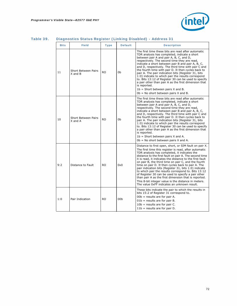
72
Programmer’s Visible State—82577 GbE PHY
11 Short Between Pairs X and B RO 0b
The first time these bits are read after automatic TDR analysis has completed, indicate a short between pair A and pair A, B, C, and D, respectively. The second time they are read, indicate a short between pair B and pair A, B, C, and D, respectively. The third time with pair C and the fourth time with pair D. It then cycles back to pair A. The pair indication bits (Register 31, bits 1:0) indicate to which pair the results correspond to. Bits 13:12 of Register 30 can be used to specify a pair other than pair A as the first dimension that is reported.1b = Short between pairs X and B.0b = No short between pairs X and B.
10 Short Between Pairs X and A RO 0b
The first time these bits are read after automatic TDR analysis has completed, indicate a short between pair A and pair A, B, C, and D, respectively. The second time they are read, indicate a short between pair B and pair A, B, C, and D, respectively. The third time with pair C and the fourth time with pair D. It then cycles back to pair A. The pair indication bits (Register 31, bits 1:0) indicate to which pair the results correspond to. Bits 13:12 of Register 30 can be used to specify a pair other than pair A as the first dimension that is reported.1b = Short between pairs X and A.0b = No short between pairs X and A.
9:2 Distance to Fault RO 0x0
Distance to first open, short, or SIM fault on pair X.The first time this register is read, after automatic TDR analysis has completed, it indicates the distance to the first fault on pair A. The second time it is read, it indicates the distance to the first fault on pair B, the third time on pair C, and the fourth time on pair D. It then cycles back to pair A. The pair indication bits (Register 31, bits 1:0) indicate to which pair the results correspond to. Bits 13:12 of Register 30 can be used to specify a pair other than pair A as the first dimension that is reported.This 8-bit integer value is the distance in meters. The value 0xFF indicates an unknown result.
1:0 Pair Indication RO 00b
These bits indicate the pair to which the results in bits 15:2 of Register 31 correspond to.00b = results are for pair A.01b = results are for pair B.10b = results are for pair C.11b = results are for pair D.
Table 39. Diagnostics Status Register (Linking Disabled) - Address 31
Bits Field Type Default Description

82577 GbE PHY—Programmer’s Visible State
73
Table 40. Diagnostics Status Register (Linking Enabled) - Address 31
Bits Field Type Default Description
15 Reserved Reserved.
14 Pair Swap on Pairs C and D RO 0b
If this bit is set, the PHY has detected that received pair 2 (RJ-45 pins 4 and 5) and pair 3 (RJ-45 pins 7 and 8) have crossed over.1b = Pairs C and D are swapped (1000BASE-T only).0b = Pairs C and D are not swapped (1000BASE-T only).
13 Polarity on Pair D RO 0b
1b = Polarity on pair D is inverted (1000BASE-T only).0b = Polarity on pair D is normal (1000BASE-T only).
12 Polarity on Pair C RO 0b
1b = Polarity on pair C is inverted (1000BASE-T only).0b = Polarity on pair C is normal (1000BASE-T only).
11 Polarity on Pair B RO 0b
1b = Polarity on pair B is inverted (10BASE-T or 1000BASE-T only).0b = Polarity on pair B is normal (10BASE-T or 1000BASE-T only).
10 Polarity on Pair A RO 0b
1b = Polarity on pair A is inverted (10BASE-T or 1000BASE-T only).0b = Polarity on pair A is normal (10BASE-T or 1000BASE-T only).
9:2 Cable Length RO 0b
This 8-bit integer value is the cable length in meters when the link is active. The value 0xFF indicates an unknown result.Cable length when the link is active.
1 Reserved Reserved.
0 Excessive Pair Skew RO 0b
Excessive pair skew in 1000BASE-T is detected by detecting that the scrambler has not acquired a 1000BASE-T link and cannot be brought up. In this case, the PHY usually falls back to 100BASE-TX or 10BASE-T. It is possible for other scrambler acquisition errors to be mistaken for excessive pair skew.1b = Excessive pair skew (1000BASE-T only).0b = No excessive pair skew (1000BASE-T only).

74
Programmer’s Visible State—82577 GbE PHY
8.6 Port Control Registers (Page 769)Table 41. Custom Mode Control PHY Address 01, Page 769, Register 16
Name Default Bits Description Type
Reserved 0x04 15:11 Reserved R/W
MDIO Frequency Access 0b 10
0b = Normal MDIO frequency access.1b = Reduced MDIO frequency access.Note: Required for read during cable disconnect.
R/W
Reserved 0x180 9:0 Reserved R/W
Table 42. Port General Configuration PHY Address 01, Page 769, Register 17
Name Default Bits Description Type
Tx Gate Wait IFS 01110b 15:11 Determines the size (in nibbles) of non-deferring window from CRS de-assertion. R/W
BP extension Wait 100b 10:8Additional waiting byte times after TX Gate Wait IPG expires until the Back Pressure In-band bit is cleared.
R/W
Reserved 0b 7 Reserved R/W
Active_PD_enable 0b 6
Active Power Down Enable (sD3 Enable)When set to 1b, the Intel® 5 Series Express Chipsetneeds to enter MAC power down mode.
R/W
Reserved 1b 5 Reserved. This bit is reset by power on reset only.
Host_WU_Active 0b 4 Enables host wake up from the 82577. This bit is reset by power on reset only. R/W
Wakeup clocks stop 1b 3 Wake-up clocks are stopped while wake up is disabled. R/W
MACPD_enable 1b 2
Written as 1b when the Intel® 5 Series Express Chipset needs to globally enable the MAC power down feature while the 82577 supports WoL. When set to 1b, pages 800 and 801 are enabled for configuration and Host_WU_Active, ME_WU_Active are not blocked for writes.
R/W
Reserved 00b 1:0 Reserved RO
Table 43. Power Management Control Register PHY Address 01, Page 769, Register 21
Name Default Bits Description Type
Reserved 0x00 15:9 Reserved, write to 0x00 RO
Collision threshold 0x0F 8:1 Number of retries for a collided packet. R/W
Retry late collision 0b 0 Retry late collision. R/W

82577 GbE PHY—Programmer’s Visible State
75
8.7 Statistics Registers
This register counts the number of times that a successfully transmitted packet encountered a single collision. This register only increments if transmits are enabled and the 82577 is in half-duplex mode.
Table 44. SMBus Control Register PHY Address 01, Page 769, Register 23
Name Default Bits Description Type
Reserved 0x0000 15:2 Reserved RO
dis_SMB_filtering 0b 1
When set, disables filtering of Rx packets for the SMBus. In wake up mode, this configuration is ignored and the filters are enabled.
R/W
Reserved 0b 0 Reserved. RO
Table 45. Rate Adaptation Control Register PHY Address 01, Page 769, Register 25
Name Default Bits Description Type
Reserved 0100010b 15:9 Reserved, write as read. RWP
rx_en_rxdv_preamble 1b 8 Enable generation of early preamble based on RX_DV in the receive path. R/W
rx_en_crs_preamble 0b 7 Enable generation of early preamble based on CRS in the receive path. R/W
reserved 0b 6 Reserved, write as read. RWP
rx_flip_bad_sfd 1b 5 Align the packet’s start of frame delimiter to a byte boundary in the receive path. R/W
read_delay_fd 10001b 4:0 Reserved, write as read. RWP
Table 46. Flow Control Transmit Timer Value PHY Address 01, Page 769, Register 27
Name Default Bits Description Type
Flow Control Transmit Timer Value 0x0000 15:0
The TTV field is inserted into a transmitted frame (either XOFF frames or any pause frame value in any software transmitted packets). It counts in units of slot time. If software needs to send an XON frame, it must set TTV to 0x0000 prior to initiating the pause frame.
RW
Table 47. Single Collision Count - SCC PHY Address 01, Page 778, Registers 16 - 17
Bit Type Reset Description
31:0 RO/V 0x00SCCNumber of times a transmit encountered a single collision.
Table 48. Excessive Collisions Count - ECOL PHY Address 01, Page 778, Register 18 - 19
Bit Type Reset Description
31:0 RO/V 0x00ECCNumber of packets with more than 16 collisions.

76
Programmer’s Visible State—82577 GbE PHY
When 16 or more collisions have occurred on a packet, this register increments, regardless of the value of collision threshold. If collision threshold is set below 16, this counter won’t increment. This register only increments if transmits are enabled and the 82577 is in half-duplex mode.
This register counts the number of times that a transmit encountered more than one collision but less than 16. This register only increments if transmits are enabled and the 82577 is in half-duplex mode.
Late collisions are collisions that occur after one slot time. This register only increments if transmits are enabled and the 82577 is in half-duplex mode.
This register counts the total number of collisions seen by the transmitter. This register only increments if transmits are enabled and the 82577 is in half-duplex mode. This register applies to clear as well as secure traffic.
This register counts defer events. A defer event occurs when the transmitter cannot immediately send a packet due to the medium busy either because another device is transmitting, the IPG timer has not expired, half-duplex deferral events, reception of XOFF frames, or the link is not up. This register only increment if transmits are enabled. The behavior of this counter is slightly different in the 82577 relative to the 82542. For the 82577, this counter does not increment for streaming transmits that are deferred due to TX IPG.
This register counts the number of successful packet transmission in which the CRS input from the 82577 was not asserted within one slot time of start of transmission from the MAC. Start of transmission is defined as the assertion of TX_EN to the 82577.
Table 49. Multiple Collision Count - MCC PHY Address 01, Page 778, Register 20 - 21
Bit Type Reset Description
31:0 RO/V 0x00MCCNumber of times a successful transmit encountered multiple collisions.
Table 50. Late Collisions Count - LATECOL PHY Address 01, Page 778, Register 23 - 24
Bit Type Reset Description
31:0 RO/V 0x00LCCNumber of packets with late collisions.
Table 51. Collision Count - COLC PHY Address 01, Page 778, Register 25 - 26
Bit Type Reset Description
31:0 RO/V 0x00COLCTotal number of collisions experienced by the transmitter.
Table 52. Defer Count - DC PHY Address 01, Page 778, Register 27 - 28
Bit Type Reset Description
31:0 RO/V 0x00CDCNumber of defer events.
Table 53. Transmit with No CRS - TNCRS PHY Address 01, Page 778, Register 29 - 30
Bit Type Reset Description
31:0 RO/V 0x00TNCRSNumber of transmissions without a CRS assertion from the 82577.

82577 GbE PHY—Programmer’s Visible State
77
The 82577 should assert CRS during every transmission. Failure to do so might indicate that the link has failed, or the 82577 has an incorrect link configuration. This register only increments if transmits are enabled. This register is only valid when the 82577 is operating at half duplex.
8.8 PCIe RegistersTable 54. PCIe FIFOs Control/Status PHY Address 01, Page 770, Register 16)
Name Default Bits Description Type
Reserved 0000001b 15:9 Reserved RO
Rx FIFO overflow 0b 8 Rx FIFO overflow occurred. RO/SC
Reserved 0b 7 Reserved RO
Tx FIFO overflow 0b 6 Tx FIFO overflow occurred. RO/SC
Reserved 000000b 5:0 Reserved RO
Table 55. PCIe Power Management Control PHY Address 01, Page 770, Register 17
Name Default Bits Description Type
Burst enable 1b 15
Burst in 10/100 Mb/s Enable1b = Bursting at 10/100 Mb/s speed is enabled.0b = Bursting disabled at 10/100 Mb/s.
RW
Reserved 00b 14:13 Reserved R/W
Reserved 000b 12:10 Reserved. RO
Reserved 10b 9:8 Reserved. R/W
Reserved 1b 7 Reserved R/W
Reserved 00b 6:5 Reserved R/W
Reserved 0010b 4:1 Reserved R/W
Reserved 0b 0B Reserved R/W

78
Programmer’s Visible State—82577 GbE PHY
Table 56. In-Band Control PHY Address 01, Page 770, Register 181
Name Default Bits Description Type
Link status transmit timeout 0x5 15:8 Link status retransmission period in tens of microseconds. R/W
pcie_pad_use_dis 0b 7 Disables 1000 Mb/s in-band messages during packets in 10/100 Mb/s mode. R/W
Max retries 0x7 6:0 Maximum retries when not receiving an acknowledge to an in-band message. R/W
1. All in-band timeouts are multiplied by 1000 while in SMBus mode.
Table 57. PCIe Diagnostic PHY Address 01, Page 770, Register 201
Name Default Bits Description Type
Reserved 0x55 15:8 Reserved, write as read. R/W
In-band status acknowledge timeout 0x04 7:0 Timeout in microseconds for receiving an
acknowledge for an in-band status message. R/W
1. All in-band timeouts are multiplied by 1000 while in SMBus mode.
Table 58. Timeouts PHY Address 01, Page 770, Register 211
Name Default Bits Description Type
Reserved 0000b 15:12 Reserved, write as read. RWP
Reserved 010100b 11:6 Reserved R/W
Reserved 010100b 5:0 Reserved R/W
1. All in-band timeouts are multiplied by 1000 while in SMBus mode.
Table 59. PCIe Kstate Minimum Duration Timeout PHY Address 01, Page 770, Register 231
Name Default Bits Description Type
Reserved 0x00 15:5 Reserved, write as read. RWP
EI_min_dur timeout 0x10 4:0These bits define the minimum time the 82577 stays in electrical idle state once entered (each bit represents 80 ns).
R/W
1. All in-band timeouts are multiplied by 1000 while in SMBus mode.

82577 GbE PHY—Programmer’s Visible State
79
8.9 General Registers
The 82577 Capability register is loaded with the set of capabilities that correspond to the selected the 82577 SKU. A change in SKU is reflected in a change in this register. A capability is enabled when its corresponding bit is set to 1b.
Table 60. 82577 Capability PHY Address 01, Page 776, Register 19
Name Default Bits Description Type
Reserved 000000b 15:10 Reserved for future capabilities. RO
Reserved 0b 9 Reserved RO
802.1Q & 802.1p 0b 8802.1Q & 802.1pEnables support for VLAN per 802.1Q & 802.1p.
RO
Receive Side Scaling 0b 7Receive Side Scaling (RSS)Enables RSS.
RO
2 Tx and 2 Rx Queues 0b 6
Two Tx and 2 Rx QueuesWhen set, enables dual transmit and dual receive queues. When cleared, a single receive and a single transmit queue are enabled.
RO
Energy Detect 0b 5Energy DetectEnables energy detect capability.
RO
AC/DC Auto Link Speed Connect 0b 4
AC/DC Auto Link Speed ConnectEnables different power management policy in AC and battery modes.
RO
Reserved 0b 3 Reserved RO
Reserved 00b 2:1 Reserved RO
Ability to initiate a team 0b 0 Ability to initiate a team; enables teaming capability. RO
Table 61. OEM Bits PHY Address 01, Page 0, Register 25
Bits Field Mode HW Rst Description
15:11 Reserved R/W 00000b
10 Aneg_now R/W 0b Restart auto-negotiation. This bit is self clearing.
9:7 Reserved R/W 000b
6 a1000_dis R/W 0b1 When set to 1b, 1000 Mb/s speed is disabled.
5:3 Reserved R/W 000b
2 rev_aneg R/W 0bLow Power Link Up mechanism. Allows a link to come up at the lowest possible speed in cases where power is more important than performance.
1:0 Reserved R/W 00b
1. 0b is the default value after power on reset. When PE_RST_N goes low (switches to SMBus), its value becomes1b.

80
Programmer’s Visible State—82577 GbE PHY
Table 62. SMBus Address PHY Address 01, Page 0, Register 261
Name Default Bits Description Type
Reserved 0x00 15:12 Reserved RO
SMB fragments size 0b 11Select SMBus Fragments SizeWhen set to 1b, the fragment size is 64 bytes, otherwise 32 bytes.
RW
APM Enable 0b 10 APM WoL enable. RW
PEC Enable 1b 9 Defines if the 82577 supports PEC on the SMBus. RW
SMBus Frequency 0b 80b = 100 KHz.1b = Reserved
RW
SMBus Address Valid 0b 7
0b = Address not valid.1b = SMBus address valid.This bit is written by the MAC when the SMBus Address field is updated. The 82577 cannot send SMBus transactions to the MAC unless this bit is set.
RW
SMBus Address 0x00 6:0 This is the MAC SMBus address. The 82577 uses it for master functionality. RW
1. This register is reset only on internal power on reset.
Table 63. Shadow Receive Address Low0 – SRAL0 PHY Address 01, Page 0, Registers 27-28
Attribute Bit(s) Initial Value Description
RW 31:0 XReceive Address Low (RAL)The lower 32 bits of the 48-bit Ethernet address n (n=0, 1…6). RAL 0 is loaded from words 0x0 and 0x1 in the NVM.
Table 64. Shadow Receive Address High0 – RAH0 PHY Address 01, Page 0, Registers 29
Attribute Bit(s) Initial Value Description
RW 15:0 XReceive Address High (RAH)The upper 16 bits of the 48-bit Ethernet address n (n=0, 1…6). RAH 0 is loaded from word 0x2 in the NVM.
RW 17:16 X
Address Select (ASEL)Selects how the address is to be used and is decoded as follows:00b = Destination address (must be set to this in normal mode).01b = Source address.10b = Reserved.11b = Reserved.
RO 30:18 0x00 Reserved, reads as 0b and ignored on writes.
RW 31 See Desc.
Address valid (AV)Cleared after master reset. If the NVM is present, the Address Valid field of Receive Address Register 0 is set to one after a software or PCI reset or NVM read.This bit is cleared by a master (software) reset.

82577 GbE PHY—Programmer’s Visible State
81
NOTES:1. When LED Blink mode is enabled the appropriate Led Invert bit should be set to zero.2. The dynamic LED's modes (LINK/ACTIVITY and ACTIVITY) should be used with LED Blink mode enabled.
8.9.1 Interrupts
The 82577 maintains status bits (per interrupt cause) to reflect the source of the interrupt request. System software is expected to clear these status bits once the interrupt is being handled.
Table 65. LED Configuration PHY Address 01, Page 0, Register 30
Name Default Bits Description Type
Blink rate 0b 15Specifies the blink mode of the LEDs.0b = Blinks at 200 ms on and 200 ms off.1b = Blinks at 83 ms on and 83 ms off.
RW
LED2 Blink 0b 14LED2_BLINK Field0b = No blinking.1b = Blinking.
RW
LED2 Invert 0b 13LED2_IVRT Field0b = Active low output.1b = Active high output.
RW
LED2 Mode 110b 12:10 Mode specifying what event/state/pattern is displayed on LED2. RW
LED1 Blink 0b 9LED1_BLINK Field0b = No blinking.1b = Blinking.
RW
LED1 Invert 0b 8LED1_IVRT Field0b = Active low output.1b = Active high output.
RW
LED1 Mode 111b 7:5 Mode specifying what event/state/pattern is displayed on LED1. RW
LED0 Blink 1b 4LED0_BLINK Field0b = No blinking.1b = Blinking.
RW
LED0 Invert 0b 3LED0_IVRT Field0b = Active low output.1b = Active high output.
RW
LED0 Mode 100b 2:0 Mode specifying what event/state/pattern is displayed on LED0. RW

82
Programmer’s Visible State—82577 GbE PHY
8.10 Wake Up Registers
8.10.1 Accessing Wake Up Registers Using MDIC
When software needs to configure the wake up state (either read or write to these registers) the MDIO page should be set to 800 (for host accesses) until the page is not changed to a different value wake up register access is enabled. After the page was set to the wake up page, the address field is no longer translated as reg_addr (register address) but as an instruction. If the given address is in the [0..15] range, meaning PHY registers, the functionality remains unchanged. There are two valid instructions:
1. Address Set – 0x11 – Wake up space address is set for either reading or writing.2. Data cycle – 0x12 – Wake up space accesses read or write cycle.
For the 82577 the wake area read cycle sequence of events is as follows:
1. Setting page 800; the software device driver performs a write cycle to the MDI register with:a. Ready = 0bb. Op-Code = 01b (write)c. PHYADD = The 82577’s address from the MDI registerd. REGADD = Page settinge. DATA = 800 (wake up page)
2. Address setting; the software device driver performs a write cycle to the MDI register with:a. Ready = 0bb. Op-Code = 01b (write)c. PHYADD = The 82577’s address from the MDI registerd. REGADD = 0x11 (address set)e. DATA = XXXX (address of the register to be read)
3. Reading a register; the software device driver performs a write cycle to the MDI register with:a. Ready = 0bb. Op-Code = 10b (read)c. PHYADD = The 82577’s address from the MDI registerd. REGADD = 0x12 (data cycle for read)e. DATA = YYYY (data is valid when the ready bit is set)
For the 82577, the wake area write cycle sequence of events is as follows:
1. Setting page 800; the software device driver performs a write cycle to the MDI register with:a. Ready = 0bb. Op-Code = 01b (write)c. PHYADD = The 82577’s address from the MDI registerd. REGADD = Page settinge. DATA = 800 (wake up page)

82577 GbE PHY—Programmer’s Visible State
83
2. Address setting; The software device driver performs a write cycle to the MDI register with:a. Ready = 0bb. Op-Code = 01b (write)c. PHYADD = The 82577’s address from the MDI registerd. REGADD = 0x11 (address set)e. DATA = XXXX (address of the register to be read)
3. Writing a register; the software device driver performs a write cycle to the MDI register with:a. Ready = 0bb. Op-Code = 01b (write)c. PHYADD = The 82577’s address from the MDI registerd. REGADD = 0x12 (data cycle for write)e. DATA = YYYY (data to be written to the register)
8.10.2 Host Wake Up Control Status Register Description
Table 66. Receive Control – RCTL PHY Address 01, Page 800, Register 0
Attribute Bit(s) Initial Value Description
RW 0 0bUnicast Promiscuous Enable (UPE)0b = Disabled.1b = Enabled.
RW 1 0bMulticast Promiscuous Enable (MPE)0b = Disabled.1b = Enabled.
RW 2 1bSlave Access Enable0b = Access disabled, the filters are active.1b = Access enabled, the filters are not active.
RW 4:3 00b
Multicast Offset (MO)This determines which bits of the incoming multicast address are used in looking up the bit vector.00b = [47:38].01b = [46:37].10b = [45:36].11b = [43:34].
RW 5 0bBroadcast Accept Mode (BAM)0b = Ignore broadcast (unless it matches through exact or imperfect filters)1b = Accept broadcast packets.
RW 6 0bPass MAC Control Frames (PMCF).0b = Do not (specially) pass MAC control frames.1b = Pass any MAC control frame (type field value of 0x8808).
RW 7 0bReceive Flow Control Enable (RFCE)Indicates that the 82577 responds to the reception of flow control packets. If auto-negotiation is enabled, this bit is set to the negotiated duplex value.
RW 8 0b Reserved
RW 15:9 0x00 Reserved

84
Programmer’s Visible State—82577 GbE PHY
Note: All wake up registers (page 800-801 except CTRL and IPAV) are not cleared with PHY reset is asserted. It is only cleared when internal power on reset is de-asserted or when cleared by the software device driver.
Note: Access to page 800/801 should be done only in 10 Mb/s and 100 Mb/s.
PMCF controls the usage of MAC control frames (including flow control). A MAC control frame in this context must be addressed to the flow control multicast address 0x0100_00C2_8001 and match the type field (0x8808). If PMCF=1b, then frames meeting this criteria participate in wake up filtering.
Table 67. Wake Up Control – WUC PHY Address 01, Page 800, Register 1
Attribute Bit(s) Initial Value Description
RW/SN 0 0bAdvance Power Management Enable (APME)If set to 1b, APM wake up is enabled.
RW/V 1 0bPME_EnIf set to 1b, ACPI wake up is enabled.
RWC 2 0bPME_StatusThis bit is set when the 82577 receives a wake up event.
RO 3 0b Reserved
RW/SN 4 0bLink Status Change Wake Enable (LSCWE)Enables wake on link status change as part of APM wake capabilities.
RW/SN 5 0b
Link Status Change Wake Override (LSCWO)If set to 1b, wake on link status change does not depend on the LNKC bit in the WUFC register. Instead, it is determined by the APM settings in the WUC register.
RO 15:6 0x00 Reserved

82577 GbE PHY—Programmer’s Visible State
85
This register is used to enable each of the pre-defined and flexible filters for wake up support. A value of 1b means the filter is turned on, and a value of 0b means the filter is turned off.
Table 68. Wake Up Filter Control – WUFC PHY Address 01, Page 800, Register 2
Attribute Bit(s) Initial Value Description
RW 0 0bLNKCLink status change wake up enable.
RW 1 0bMAGMagic packet wake up enable.
RW 2 0bEXDirected exact wake up enable.
RW 3 0bMCDirected multicast wake up enable.
RW 4 0bBCBroadcast wake up enable.
RW 5 0b IPv4 request packet wake up enable.
RW 6 0bIPV4Directed IPv4 packet wake up enable.
RW 7 0bIPV6Directed IPv6 packet wake up enable.
RO 8 0b Reserved.
RW 9 0FLX4Flexible filter 3 enable.
RW 10 0bFLX5Flexible filter 3 enable.
RW 11 0b
NoTCOIgnore TCO packets for host wake up. If the NoTCO bit is set, then any packet that passes the manageability packet filtering does not cause a host wake up event even if it passes one of the host wake up filters.
RW 12 0bFLX0Flexible filter 0 enable
RW 13 0bFLX1Flexible filter 1 enable
RW 14 0bFLX2Flexible filter 2 enable
RW 15 0bFLX3Flexible filter 3 enable

86
Programmer’s Visible State—82577 GbE PHY
This register is used to record statistics about all wake up packets received. Note that packets that match multiple criteria might set multiple bits. Writing a 1b to any bit clears that bit.
This register is not cleared when PHY reset is asserted. It is only cleared when internal power on reset is de-asserted or when cleared by the software device driver.
Table 69. Wake Up Status – WUS PHY Address 01, Page 800, Register 3
Attribute Bit(s) Initial Value Description
RWC 0 0bLNKCLink status changed
RWC 1 0bMAGMagic packet received
RWC 2 0bEXDirected exact packet received. The packet’s address matched one of the 7 pre-programmed exact values in the Receive Address registers.
RWC 3 0bMCDirected multicast packet received. The packet was a multicast packet that was hashed to a value that corresponded to a 1-bit in the multicast table array.
RWC 4 0bBCBroadcast packet received.
RWC 5 0b IPv4 request packet received.
RWC 6 0bIPV4Directed IPv4 packet received.
RWC 7 0bIPV6Directed IPv6 packet received.
RO 8 0b Reserved, read as 0b.
RWC 9 0bFLX4Flexible filter 4 match.
RWC 10 0bFLX5Flexible filter 5 match.
RO 11 0b Reserved.
RWC 12 0bFLX0Flexible filter 0 match.
RWC 13 0bFLX1Flexible filter 1 match.
RWC 14 0bFLX2Flexible filter 2 match.
RWC 15 0bFLX3Flexible filter 3 match.

82577 GbE PHY—Programmer’s Visible State
87
AV determines whether this address is compared against the incoming packet. AV is cleared by a master (software) reset.
ASEL enables the 82577 to perform special filtering on receive packets.
Note: RAR0 should always be used to store the individual Ethernet MAC address of the Network Interface Card (NIC).
After reset, if the NVM is present, the first register (Receive Address Register 0) is loaded from the IA field in the NVM, its Address Select field is 00b, and its Address Valid field is 1b. If no NVM is present the Address Valid field is 0b. The Address Valid field for all of the other registers are 0b.
Table 70. Receive Address Low – RAL PHY Address 01, Page 800, Registers 16-17 + 4*n1 (n=0…6)
Attribute Bit(s) Initial Value Description
RW 31:0 0Receive Address Low (RAL)The lower 32 bits of the 48-bit Ethernet address n (n=0, 1…6). RAL 0 is loaded from words 0x0 and 0x1 in the NVM.
1. While “n” is the exact unicast/multicast address entry and it is equals to 0,1,…6.
Table 71. Receive Address High – RAH PHY Address 01, Page 800, Registers 18-19 + 4*n1 (n=0…6)
Attribute Bit(s) Initial Value Description
RW 15:0 XReceive Address High (RAH)The upper 16 bits of the 48-bit Ethernet address n (n=0, 1…6). RAH 0 is loaded from word 0x2 in the NVM.
RW 17:16 X
Address Select (ASEL)Selects how the address is to be used and is decoded as follows:00b = Destination address (must be set to this in normal mode).01b = Source address.10b = Reserved.11b = Reserved.
RO 30:18 0x00 Reserved, reads as 0b and ignored on writes.
RW 31 See Desc.
Address valid (AV)Cleared after master reset. If the NVM is present, the Address Valid field of Receive Address Register 0 is set to one after a software or PCI reset or NVM read.This bit is cleared by a master (software) reset.
1. While “n” is the exact unicast/Multicast address entry and it is equals to 0,1,…6

88
Programmer’s Visible State—82577 GbE PHY
.
Table 72. Shared Receive Address Low – SHRAL PHY Address 01, Page 800, Registers 44-45 + 4*n (n=0…3)
Attribute Bit(s) Initial Value Description
RW 31:0 XReceive Address Low (RAL)The lower 32 bits of the 48-bit Ethernet address n (n=0…3).
Table 73. Shared Receive Address High – SHRAH PHY Address 01, Page 800, Registers 46-47 + 4*n (n=0…2)
Attribute Bit(s) Initial Value Description
RW 15:0 XReceive Address High (RAH)The upper 16 bits of the 48-bit Ethernet address n (n=0…3).
RO 17:16 0x00Address Select (ASEL)Selects how the address is to be used. 00b means that it is used to decode the destination MAC address.
RO 30:18 0x00 Reserved, reads as 0b and is ignored on writes.
RW 31 0bAddress valid (AV)When this bit is set, the relevant RAL and RAH are valid (compared against the incoming packet).
Table 74. Shared Receive Address High 3 – SHRAH[3] PHY Address 01, Page 800, Registers 58-59
Attribute Bit(s) Initial Value Description
RW 15:0 XReceive Address High (RAH)The upper 16 bits of the 48-bit Ethernet address n (n=0…3).
RO 17:16 00bAddress Select (ASEL)Selects how the address is to be used. 00b means that it is used to decode the destination MAC address.
RO 29:18 0x00 Reserved, reads as 0x00 and is ignored on writes.
RW 30 0bAll Nodes Multicast Address valid (MAV)The all nodes multicast address (33:33:00:00:00:01) is valid when this bit is set. Note that 0x33 is the first byte on the wire.
RW 31 0bAddress valid (AV)When this bit is set, the relevant address 3 is valid (compared against the incoming packet).

82577 GbE PHY—Programmer’s Visible State
89
The IPv6 address table is used to store the IPv6 addresses for directed IPv6 packet wake ups and manageability traffic filtering.
IP6AT can be used by the host.
There is one register per 32 bits of the multicast address table for a total of 32 registers (thus the MTA[31:0] designation). The size of the word array depends on the number of bits implemented in the multicast address table. Software must mask to the desired bit on reads and supply a 32-bit word on writes.
Note: All accesses to this table must be 32-bit.
Table 75. IP Address Valid – IPAV1 PHY Address 01, Page 800, Register 64
Attribute Bit(s) Initial Value Description
RO 0 0b Reserved
RW 1 0bV41IPv4 address 1 valid.
RW 2 0bV42IPv4 address 2 valid.
RW 3 0bV43IPv4 address 3 valid.
RO 4:14 0x00 Reserved
RW 15 0bV60IPv6 address valid.
1. The IP address valid indicates whether the IP addresses in the IP address table are valid.
Table 76. IPv4 Address Table – IP4AT1 PHY Address 01, Page 800, Registers 82-83 + 2*n (n=0, 1, 2)
Attribute Bit(s) Initial Value Description
RW 31:0 XIPADDIP address n (n= 0, 1, 2).
1. The IPv4 address table is used to store the three IPv4 addresses for IPv4 request packets and directed IPv4packet wake ups. It is a 3-entry table with the following format:
Table 77. IPv6 Address Table – IP6AT PHY Address 01, Page 800, Registers 88-89 + 2*n (n=0…3)
Attribute Bit(s) Initial Value Description
RW 31:0 XIPV6 AddressIPv6 address bytes n*4…n*4+3 (n=0, 1, 2, 3) while byte 0 is first on the wire and byte 15 is last.
Table 78. Multicast Table Array – MTA[31:0] PHY Address 01, Page 800, Registers 128-191
Attribute Bit(s) Initial Value Description
RW 31:0 XBit Vector.Word-wide bit vector specifying 32 bits in the multicast address filter table.

90
Programmer’s Visible State—82577 GbE PHY
Figure 9 shows the multicast lookup algorithm. The destination address shown represents the internally stored ordering of the received destination address. Note that Byte 1 bit 0 shown in Figure 9 is the first on the wire. The bits that are directed to the multicast table array in this diagram match a multicast offset in the CTRL register equals 00b. The complete multicast offset options are:
Figure 9. Multicast Table Array Algorithm
There are 128 filter values. The flexible filter value is used to store the one value for each byte location in a packet for each flexible filter. If the corresponding mask bit is one, then the flexible filter compares the incoming data byte to the values stored in this table.
Multicast Offset Bits Directed to the Multicast Table Array
00b DA[47:38] = Byte 6 bits 7:0, Byte 5 bits 1:0
01b DA[46:37] = Byte 6 bits 6:0, Byte 5 bits 2:0
10b DA[45:36] = Byte 6 bits 5:0, Byte 5 bits 3:0
11b DA[43:34] = Byte 6 bits 3:0, Byte 5 bits 5:0
Table 79. Flexible Filter Value Table LSB– FFVT_01 PHY Address 01, Page 800, Registers 256 + 2*n (n=0…127)
Attribute Bit(s) Initial Value Description
RW 7:0 XValue 0Value of filter 0 byte n (n=0, 1… 127).
RW 15:8 XValue 1Value of filter 1 byte n (n=0, 1… 127).

82577 GbE PHY—Programmer’s Visible State
91
In the 82577 since each address contains 16 bits, only the least significant bytes are stored in those addresses.
There are 128 filter values. The flexible filter value is used to store the one value for each byte location in a packet for each flexible filter. If the corresponding mask bit is one, then the flexible filter compares the incoming data byte to the values stored in this table.
In the 82577 since each address contains 16 bits, only the most significant bytes are stored in those addresses.
Note: Before writing to the flexible filter value table the software device driver must first disable the flexible filters by writing zeros to the Flexible Filter Enable bits of the WUFC register (WUFC.FLXn).
Table 80. Flexible Filter Value Table MSBs – FFVT_23 PHY Address 01, Page 800, Registers 257 + 2*n (n=0…127)
Attribute Bit(s) Initial Value Description
RW 7:0 XValue 2Value of filter 2 byte n (n=0, 1… 127).
RW 15:8 XValue 3Value of filter 3 byte n (n=0, 1… 127).
Table 81. Flexible Filter Value Table – FFVT_45 PHY Address 01, Page 800, Registers 512 + 2*n (n=0…127)
Attribute Bit(s) Initial Value Description
RW 7:0 XValue 4Value of filter 4 byte n (n=0, 1… 127).
RW 15:8 XValue 5Value of filter 5 byte n (n=0, 1… 127).
Table 82. Flexible Filter Mask Table – FFMT PHY Address 01, Page 800, Registers 768 + n (n=0…127)
Attribute Bit(s) Initial Value Description
RW 0 XMask 0Mask for filter 0 byte n (n=0, 1… 127).
RW 1 XMask 1Mask for filter 1 byte n (n=0, 1… 127).
RW 2 XMask 2Mask for filter 2 byte n (n=0, 1… 127).
RW 3 XMask 3Mask for filter 3 byte n (n=0, 1… 127).
RW 4 XMask 4Mask for filter 3 byte n (n=0, 1… 127).
RW 5 XMask 5Mask for filter 3 byte n (n=0, 1… 127).
RO 15:6 X Reserved.

92
Programmer’s Visible State—82577 GbE PHY
There are 128 mask entries. The flexible filter mask and table is used to store the four 1-bit masks for each of the first 128 data bytes in a packet, one for each flexible filter. If the mask bit is one, the corresponding flexible filter compares the incoming data byte at the index of the mask bit to the data byte stored in the flexible filter value table.
Note: Before writing to the flexible filter mask table the software device driver must first disable the flexible filters by writing zeros to the Flexible Filter Enable bits of the WUFC register (WUFC.FLXn).
All reserved fields read as zeros and are ignored on writes.
There are four flexible filters lengths. The flexible filter length table stores the minimum packet lengths required to pass each of the flexible filters. Any packets that are shorter than the programmed length won’t pass that filter. Each flexible filter considers a packet that doesn’t have any mismatches up to that point to have passed the flexible filter when it reaches the required length. It does not check any bytes past that point.
Note: Before writing to the flexible filter length table the software device driver must first disable the flexible filters by writing zeros to the Flexible Filter Enable bits of the WUFC register (WUFC.FLXn).
Table 83. Flexible Filter Length Table – FFLT03 PHY Address 01, Page 800, Registers 896 + n (n=0…3)
Attribute Bit(s) Initial Value Description
RW 10:0 XLENMinimum length for flexible filter n (n=0, 1… 3).
RO 15:11 X Reserved.
Table 84. Flexible Filter Length Table – FFLT45 PHY Address 01, Page 800, Registers 904 + n (n=0…1)
Attribute Bit(s) Initial Value Description
RW 10:0 XLENMinimum Length for Flexible Filter n (n=0, 1).
RO 15:11 X Reserved.

82577 GbE PHY—Non-Volatile Memory (NVM)
93
9.0 Non-Volatile Memory (NVM)
9.1 IntroductionThis section is intended for designs using a 10/100/1000 Mb/s MAC that is integrated into an Intel® 5 Series Express Chipset in conjunction with an the 82577 Physical Layer Transceiver (PHY).
There are several LAN clients that might access the NVM such as hardware, LAN driver, and BIOS. Refer to the Intel® 5 Series Express Chipset Family External Design Specification (Intel® 5 Series Express Chipset EDS) and the Intel® 5 Series Express Chipset SPI Programming Guide for more details.
Unless otherwise specified, all numbers in this section use the following numbering convention:
• Numbers that do not have a suffix are decimal (base 10).• Numbers with a prefix of “0x” are hexadecimal (base 16).• Numbers with a suffix of “b” are binary (base 2).
9.2 NVM Programming Procedure OverviewThe LAN NVM shares space on an SPI Flash device (or devices) along with the BIOS, Manageability Firmware, and a Flash Descriptor Region. It is programmed through the Intel® 5 Series Express Chipset. This combined image is shown in Figure 10. The Flash Descriptor Region is used to define vendor specific information and the location, allocated space, and read and write permissions for each region. The Manageability (ME) Region contains the code and configuration data for ME functions such as Intel® Active Management Technology. The system BIOS is contained in the BIOS Region. The ME Region and BIOS Region are beyond the scope of this document and a more detailed explanation of these areas can be found in the Intel® 5 Series Express Chipset Family External Design Specification (Intel® 5 Series Express Chipset EDS). This document describes the LAN image contained in the Gigabit Ethernet (GbE) region.

94
Non-Volatile Memory (NVM)—82577 GbE PHY
Figure 10. LAN NVM Regions
To access the NVM, it is essential to correctly setup the following:1. A valid Flash Descriptor Region must be present. Details for the Flash Descriptor
Region are contained in the Intel® 5 Series Express Chipset EDS. This process is described in detail in the Intel® Active Management Technology OEM Bring-Up Guide.The Intel® Active Management Technology OEM Bring-Up Guide can be obtained by contacting your local Intel representative.
2. The GbE region must be part of the original image flashed onto the part.3. For Intel LAN tools and drivers to work correctly, the BIOS must set the VSCC
register(s) correctly. There are two sets of VSCC registers, the upper (UVSCC) and lower (LVSCC). Note that the LVSCC register is only used if the NVM attributes change. For example, the use of a second flash component, a change in erase size between segments, etc. Due to the architecture of the Intel® 5 Series Express Chipset, if these registers are not set correctly, the LAN tools might not report an error message even though the NVM contents remain unchanged. Refer to the Intel® 5 Series Express Chipset EDS for more information

82577 GbE PHY—Non-Volatile Memory (NVM)
95
4. The GbE region of the NVM must be accessible. To keep this region accessible, the Protected Range register of the GbE LAN Memory Mapped Configuration registers must be set to their default value of 0x0000 0000. (The GbE Protected Range registers are described in the Intel® 5 Series Express Chipset EDS).
5. The sector size of the NVM must equal 256 bytes, 4 KB, or 64 KB. When a Flash device that uses a 64 KB sector erase is used, the GbE region size must equal 128 KB. If the Flash part uses a 4 KB or 256-byte sector erase, then the GbE region size must be set to 8 KB.
The NVM image contains both static and dynamic data. The static data is the basic platform configuration, and includes OEM specific configuration bits as well as the unique Printed Circuit Board Assembly (PBA). The dynamic data holds the product’s Ethernet Individual Address (IA) and Checksum. This file can be created using a text editor.
9.3 LAN NVM Format and ContentsTable 11 lists the NVM maps for the LAN region. Each word listed is described in detail in the following sections.
Table 11. LAN NVM Address Map
LANWordOffset
NVMByte
OffsetUsedBy 15 0 Image
Value
0x00 0x00 HW-Shared Ethernet Address Byte 2, 1 IA (2, 1)
0x01 0x02 HW-Shared Ethernet Address Byte 4, 3 IA (4, 3)
0x02 0x04 HW-Shared Ethernet Address Byte 6, 5 IA (6, 5)
0x03 0x06 SW Reserved 0x0800
0x04 0x08 SW Reserved 0xFFFF
0x05 0x0A SW Image Version Information 1
0x06 0x0C SW Reserved 0xFFFF
0x07 0x0E SW Reserved 0xFFFF
0x08 0x10 SW PBA Low
0x09 0x12 SW PBA High
0x0A 0x14 HW-PCI PCI Init Control Word
0x0B 0x16 HW-PCI Subsystem ID
0x0C 0x18 HW-PCI Subsystem Vendor ID
0x0D 0x1A HW-PCI Device ID 0x10EA
0x0E 0x1C HW-PCI Reserved
0x0F 0x1E HW-PCI Reserved
0x10 0x20 HW-PCI LAN Power Consumption
0x11 0x22 HW Reserved
0x12 0x24 Reserved
0x13 0x26 HW-Shared Shared Init Control Word
0x14 0x28 HW-Shared Extended Configuration Word 1
0x15 0x2A HW-Shared Extended Configuration Word 2
0x16 0x2C HW-Shared Extended Configuration Word 3
0x17 0x2E HW-Shared OEM Configuration Defaults
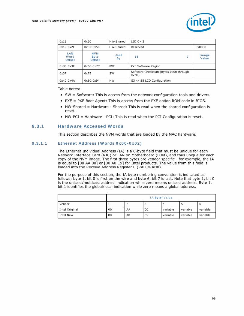
96
Non-Volatile Memory (NVM)—82577 GbE PHY
Table notes:• SW = Software: This is access from the network configuration tools and drivers.• PXE = PXE Boot Agent: This is access from the PXE option ROM code in BIOS.• HW-Shared = Hardware - Shared: This is read when the shared configuration is
reset.• HW-PCI = Hardware - PCI: This is read when the PCI Configuration is reset.
9.3.1 Hardware Accessed Words
This section describes the NVM words that are loaded by the MAC hardware.
9.3.1.1 Ethernet Address (Words 0x00-0x02)
The Ethernet Individual Address (IA) is a 6-byte field that must be unique for each Network Interface Card (NIC) or LAN on Motherboard (LOM), and thus unique for each copy of the NVM image. The first three bytes are vendor specific - for example, the IA is equal to [00 AA 00] or [00 A0 C9] for Intel products. The value from this field is loaded into the Receive Address Register 0 (RAL0/RAH0).
For the purpose of this section, the IA byte numbering convention is indicated as follows; byte 1, bit 0 is first on the wire and byte 6, bit 7 is last. Note that byte 1, bit 0 is the unicast/multicast address indication while zero means unicast address. Byte 1, bit 1 identifies the global/local indication while zero means a global address.
0x18 0x30 HW-Shared LED 0 - 2
0x19:0x2F 0x32:0x5E HW-Shared Reserved 0x0000
LANWordOffset
NVMByte
OffsetUsedBy 15 0 Image
Value
0x30:0x3E 0x60:0x7C PXE PXE Software Region
0x3F 0x7E SW Software Checksum (Bytes 0x00 through 0x7D)
0x40:0x4A 0x80:0x94 HW G3 -> S5 LCD Configuration
IA Byte/Value
Vendor 1 2 3 4 5 6
Intel Original 00 AA 00 variable variable variable
Intel New 00 A0 C9 variable variable variable

82577 GbE PHY—Non-Volatile Memory (NVM)
97
9.3.1.2 PCI Init Control Word (Word 0x0A)
This word contains initialization values that:• Sets defaults for some internal registers• Enables/disables specific features• Determines which PCI configuration space values are loaded from the NVM
9.3.1.3 Subsystem ID (Word 0x0B)
If the Load Subsystem ID in word 0x0A is set, this word is read in to initialize the Subsystem ID. Default value is 0x0000.
9.3.1.4 Subsystem Vendor ID (Word 0x0C)
If the Load Subsystem ID in word 0x0A is set, this word is read in to initialize the Subsystem Vendor ID. Default value is 0x8086.
9.3.1.5 Device ID (Word 0x0D)
If the Load Device ID in word 0x0A is set, this word is read in to initialize the Device ID of the 82577 PHY. Default value is 0x10EA.
9.3.1.6 Reserved Words 0x0E and 0x0F
Bit Name Default Description
15:13 Reserved 000b This field is reserved and must be set to 000b.
12 Reserved 1b Reserved, must be set to 1b.
11:8 Reserved 0000b These bits are reserved and must be set to 0000b.
7 AUX PWR 1b
Auxiliary Power IndicationIf set and if PM Ena is set, D3cold wake-up is advertised in the Intel® 5 Series Express Chipset of the PCI function.0b = No AUX power.1b = AUX power.
6 PM Enable 1b
Power Management Enable (PME-WoL)Enables asserting PME in the PCI function at any power state. This bit affects the advertised PME_Support indication in the Intel® 5 Series Express Chipset of the PCI function.0b = Disable.1b = Enable.
5:3 Reserved 0x0 These bits are reserved and must be set to 0x0.
2 Reserved 0b Reserved, set to 0b.
1Load Subsystem IDs
1b
Load Subsystem IDs from NVMWhen set to 1b, indicates that the device is to load its PCI Subsystem ID and Subsystem Vendor ID from the NVM (words 0Bh and 0Ch).
0 Load Device IDs 1b
Load Device ID from NVMWhen set to 1b, indicates that the device is to load its PCI Device ID from the NVM (word 0Dh).

98
Non-Volatile Memory (NVM)—82577 GbE PHY
9.3.1.7 LAN Power Consumption (Word 0x10)
This word is meaningful only if the power management is enabled.
9.3.1.8 Reserved (Word 0x11)
9.3.1.9 Reserved (Word 0x12)
9.3.1.10 Shared Init Control Word (Word 0x13)
This word controls general initialization values.
Bits Name Default Description
15:8 LAN D0 Power 0x7
The value in this field is reflected in the PCI Power Management Data register for D0 power consumption and dissipation (Data_Select = 0 or 4). Power is defined in 100 mW units. The power also includes the external logic required for the LAN function.
7:5 Reserved 000b Reserved, set to 000b.
4:0 LAN D3 Power 0x2
The value in this field is reflected in the PCI Power Management Data register for D3 power consumption and dissipation (Data_Select = 3 or 7). Power is defined in 100 mW units. The power also includes the external logic required for the LAN function. The most significant bits in the Data register that reflects the power values are padded with zeros.
Bits Name Default Description
15:0 Reserved 0x0000 Reserved, set to 0x0000.
Bits Name Default Description
15:0 Reserved 0x0000 Reserved, set to 0x0000.
Bits Name Default Description
15:14 Sign 00b
Valid IndicationA 2-bit valid indication field indicates to the device that there is a valid NVM present. If the valid field does not equal 10b the MAC does not read the rest of the NVM data and default values are used for the device configuration.
13 Reserved 1b Reserved, set to 1b.
12:10 Reserved 001b Reserved, set to 001b.
9 PHY PD Ena 0b
Enable PHY Power DownWhen set, enables PHY power down at DMoff/D3 or Dr and no WoL. This bit is loaded to the PHY Power Down Enable bit in the Extended Device Control (CTRL_EXT) register.1b = Enable PHY power down.0b = PHY always powered up.
8 Reserved 1b Reserved, should be set to 1b.

82577 GbE PHY—Non-Volatile Memory (NVM)
99
7:6 PHYT 10b
PHY Device TypeIndicates that the PHY is connected to the MAC and resulted mode of operation of the MAC/PHY link buses.00b = 82577.01b = Reserved.10b = Reserved.11b = Reserved.
5 Reserved 01 Reserved, should be set to 1b.
4 FRCSPD 0b Default setting for the Force Speed bit in the Device Control register (CTRL[11]).
3 FD 0b Default setting for the Full Duplex bit in the Device Control register (CTRL[0]). The hardware default value is 1b.
2 Reserved 1b Reserved, set to 0b.
1 CLK_CNT_1_4 0b When set, automatically reduces DMA frequency. Mapped to the Device Status register (STATUS[31]).
0 Dynamic Clock gating 1b When set, enables dynamic clock gating of the DMA and MAC
units. This bit is loaded to the DynCK bit in the CTRL_EXT register.
Bits Name Default Description

100
Non-Volatile Memory (NVM)—82577 GbE PHY
9.3.1.11 Extended Configuration Word 1 (Word 0x14)
9.3.1.12 Extended Configuration Word 2 (Word 0x15)
9.3.1.13 Extended Configuration Word 3 (Word 0x16)
Bits Name Default Description
15:14 Reserved 00b Reserved, set to 00b.
13 LCD Write Enable 0b
When set, enables loading of the extended LAN connected device configuration area in the 82577. This configuration area also includes the PHY tuning (tuning for IEEE) in the NVM. Since this bit is set to 0b by default, PHY tuning does not take effect until the LAN driver and/or firmware loads. When disabled, the extended LAN connected device configuration area is ignored. Loaded to the EXTCNF_CTRL register.
12 OEM Write Enable 0b
When set, enables auto load of the OEM bits from the PHY_CTRL register to the PHY. OEM bits include any LED configuration. Since this bit is set to 0b by default, the auto-load of OEM bits do not take effect until the LAN driver and/or firmware loads. Loaded to the Extended Configuration Control register (EXTCNF_CTRL[3]).1b = OEM bits written to the 82577.0b = No OEM bits configuration.
11:0Extended Configuration Pointer
0x28
Defines the base address (in Dwords) of the Extended Configuration area in the NVM. The base address defines an offset value relative to the beginning of the LAN space in the NVM. A value of 0x00 is not supported when operating with the 82577. Loaded to the Extended Configuration Control register (EXTCNF_CTRL[27:16]).
Bits Name Default Description
15:8 Extended PHY Length 0x00
Size (in Dwords) of the Extended PHY configuration area loaded to the Extended Configuration Size register (EXTCNF_SIZE[23:16]). If an extended configuration area is disabled by bit 13 in word 0x14, its length must be set to zero.
7:0 Reserved 0x00 Reserved, must be set to 0x00.
Bits Name Default Description
15:8 Reserved 0x00 Reserved, set to 0x00.
7:0 Reserved 0x00 Reserved, set to 0x00.

82577 GbE PHY—Non-Volatile Memory (NVM)
101
9.3.1.14 OEM Configuration Defaults (Word 0x17)
This word defines the OEM fields for the PHY power management parameters loaded to the PHY Control (PHY_CTRL) register.
Bits Name Default Description
15 Reserved 0b Reserved, set to 0b.
14 GbE Disable 0b When set, GbE operation is disabled in all power states (including D0a).
13:12 Reserved 00b Reserved, set to 00b.
11 GbE Disable in non-D0a 1b Disables GbE operation in non-D0a states. This bit must be set if GbE
Disable (bit 14) is set.
10 LPLU Enable in non-D0a 1b
Low Power Link UpEnables a decrease in link speed in non-D0a states when power policy and power management states dictate so. This bit must be set if LPLU Enable in D0a bit is set.
9 LPLU Enable in D0a 0b
Low Power Link UpEnables a decrease in link speed in all power states.
8 Reserved 0b Reserved, set to 0b.
7:0 Reserved 0x0 Reserved.

102
Non-Volatile Memory (NVM)—82577 GbE PHY
9.3.1.15 LED 0 - 2 Configuration Defaults (Word 0x18)
This NVM word specifies the hardware defaults for the LED Control (LEDCTL) register fields controlling the LED1 (LINK_1000), LED0 (LINK/ACTIVITY) and LED2 (LINK_100) output behaviors. Refer to the Intel® 5 Series Family PDG and the 82577 Reference Schematics for LED connection details. Also, Table 12 lists mode encodings for LED outputs.
Note: Due to the architecture of the 82577 the customized LEDs settings are written to the 82577 by the LAN driver. As a result, the default LEDs are written during the boot process and when resuming from power states S3, S4, and S5 to normal operation until the LAN driver writes any custom settings. This same behavior is also observed while in S3 and toggling from ac power (wall outlet) to dc power (battery). Once the LAN driver loads after a system boot or when resuming from sleep states, the LEDs function as defined in Word 0x18 of the GbE region of the NVM.
Bits Name Default Description
15 Blink Rate 0bBlink Rate0b = Blink at 200 ms on and 200 ms off.1b = Blink at 83 ms on and 83 ms off.
14 LED2 Blink 0bInitial Value of LED2_BLINK Field0b = Non-blinking.1b = Blinking.
13 LED2 Invert 0bInitial Value of LED2_IVRT Field0b = Active-low output.
12:10 LED2 Mode 110bLED2 ModeSpecifies what event/state/pattern is displayed on the LED2 output.0110b = 100 Mb/s link_up.
9 LED1 Blink 0bInitial Value of LED1_BLINK Field0b = Non-blinking.1b = Blinking.
8 LED1 Invert 0bInitial Value of LED1_IVRT Field0b = Active-low output.
7:5 LED1 Mode 111bLED1 ModeSpecifies what event/state/pattern is displayed on the LED1 output.0111b = 1000 Mb/s link_up.
4 LED0 Blink 1bInitial Value of LED0_BLINK Field0b = Non-blinking.1b = Blinking.
3 LED0 Invert 0bInitial Value of LED0_IVRT Field0b = Active-low output.
2:0 LED0 Mode 100bLED0 ModeSpecifies what event/state/pattern is displayed on the LED0 output.100b = Filter activity on.

82577 GbE PHY—Non-Volatile Memory (NVM)
103
Table 12. Mode Encodings for LED Outputs
9.3.1.16 Reserved (Word 0x19)
9.3.1.17 Reserved (Word 0x1A)
Mode Mnemonic State / Event Indicated
000b LINK_10/1000 Asserted when either 10 or 1000 Mb/s link is established and maintained.
001b LINK_100/1000 Asserted when either 100 or 1000 Mb/s link is established and maintained.
010b LINK_UP Asserted when any speed link is established and maintained.
011b ACTIVITY Asserted when link is established and packets are being transmitted or received.
100b LINK/ACTIVITY Asserted when link is established and when there is no transmit or receive activity.
101b LINK_10 Asserted when a 10 Mb/s link is established and maintained.
110b LINK_100 Asserted when a 100 Mb/s link is established and maintained.
111b LINK_1000 Asserted when a 1000 Mb/s link is established and maintained.
Bits Name Default Description
15:14 Reserved 00b Reserved, set to 00b.
13 Reserved 0b Reserved, set to 0b.
12:10 Reserved 010b Reserved, set to 010b.
9:8 Reserved 11b Reserved, set to 11b.
7 Reserved 0b Reserved, set to 0b.
6 Invalid image CSUM 0b
When cleared this bit indicates to the NVM programming tools (EEUPDATE and LANConf) that the image checksum needs to be corrected. When set, the checksum is assumed to be correct.
5:0 Reserved 0x0 Reserved, set to 0x0.
Bits Name Default Description
15:12 Reserved 0x000 Reserved, set to 0x000.
11 Reserved 1b Reserved, set to 1b.
10:7 Reserved 0000b Reserved, set to 0000b.
6 Reserved 1b Reserved, set to 1b.
5:2 Reserved 0000b Reserved, set to 0000b.
1 Reserved 1b Reserved, set to 1b.
0 APM Enable 1b
APM EnableInitial value of Advanced Power Management Wake Up Enable in the Wake Up Control (WUC.APME) register.1b = Advanced power management enabled.0b = Advanced power management disabled.

104
Non-Volatile Memory (NVM)—82577 GbE PHY
9.3.1.18 Reserved (Word 0x1B)
9.3.1.19 Reserved (Word 0x1C)
9.3.1.20 Reserved (Word 0x1D)
9.3.1.21 Reserved (Word 0x1E)
9.3.1.22 Reserved (Word 0x1F)
9.3.1.23 Reserved (Word 0x20)
9.3.1.24 Reserved (Word 0x21)
Bits Name Default Description
15:5 Reserved 0x0 Reserved, set to 0x0.
4 K1_PLL_stop_en 0b Enable PLL stop in K1.
3 K0s_100_En 0b Enables K0s mode when PHY link speed is 10/100 Mb/s.
2 K0s_GbE_En 0b Enables K0s mode when PHY link speed is 1000 Mb/s.
1 Reserved 0b Reserved, set to 0b.
0 K1_En 0b When set to 1b enables K1 low power mode.
Bits Name Default Description
15:0 Reserved 0x10EA Reserved
Bits Name Default Description
15:0 Reserved 0xBAAD Reserved
Bits Name Default Description
15:0 Reserved 0x10EA Reserved
Bits Name Default Description
15:0 Reserved 0x10EB Reserved
Bits Name Default Description
15:0 Reserved 0xBAAD Reserved
Bits Name Default Description
15:0 Reserved 0xBAAD Reserved

82577 GbE PHY—Non-Volatile Memory (NVM)
105
9.3.1.25 Reserved (Word 0x22)
9.3.1.26 Reserved (Word 0x23)
Bits Name Default Description
15:0 Reserved 0xBAAD Reserved
Bits Name Default Description
15:0 Reserved 0xBAAD Reserved

106
Non-Volatile Memory (NVM)—82577 GbE PHY
9.3.1.27 Reserved (Word 0x24)
9.3.1.28 Reserved (Word 0x25)
9.3.1.29 Reserved (Word 0x26)
9.3.1.30 Reserved (Word 0x27)
9.3.2 Software Accessed Words
9.3.2.1 PXE Words (Words 0x30 Through 0x3E)
Words 0x30 through 0x3E (bytes 0x60 through 0x7D) have been reserved for configuration and version values to be used by PXE code.
Bits Name Default Description
15 Reserved 1b Reserved, set to 1b.
14 Reserved 0b Reserved, set to 0b.
13:0 Reserved 0x0000 Reserved, set to 0x0000.
Bits Name Default Description
15 Reserved 1b Reserved, set to 1b.
14:8 Reserved 0x00 Reserved, set to 0x00.
7 Reserved 1b Reserved, set to 1b.
6:5 Reserved 00b Reserved, set to 00b.
4 Reserved 1b Reserved, set to 1b.
3:0 Reserved 0000b Reserved, set to 0000b.
Bits Name Default Description
15 Reserved 0b Reserved
14 Reserved 1b Reserved
13:12 Reserved 00b Reserved
11 Reserved 1b Reserved
10 Reserved 0b Reserved
9 Reserved 1b Reserved
8:0 Reserved 0x00 Reserved
Bits Name Default Description
15:0 Reserved 0x00 Reserved

82577 GbE PHY—Non-Volatile Memory (NVM)
107
9.3.2.1.1 Boot Agent Main Setup Options (Word 0x30)
The boot agent software configuration is controlled by the NVM with the main setup options stored in word 0x30. These options are those that can be changed by using the Control-S setup menu or by using the IBA Intel Boot Agent utility. Note that these settings only apply to Boot Agent software.
Table 13. Boot Agent Main Setup Options
Bit Name Description
15:14 Reserved Reserved, set to 00b.
13 Reserved Reserved, must be set to 0b.
12 FDPForce Full Duplex.Set this bit to 0b for half duplex and 1b for full duplex.Note that this bit is a don’t care unless bits 10 and 11 are set.
11:10 FSP
Force Speed.These bits determine speed.01b = 10 Mb/s.10b = 100 Mb/s.11b = Not allowed.All zeros indicate auto-negotiate (the current bit state).Note that bit 12 is a don’t care unless these bits are set.
9 ReservedReservedSet this bit to 0b.
8 DSM
Display Setup Message.If this bit is set to 1b, the "Press Control-S" message appears after the title message. The default for this bit is 1b.
7:6 PT
Prompt Time. These bits control how long the "Press Control-S" setup prompt message appears, if enabled by DIM.00b = 2 seconds (default).01b = 3 seconds.10b = 5 seconds.11b = 0 seconds.Note that the Ctrl-S message does not appear if 0 seconds prompt time is selected.
5 Reserved Reserved
4:3 DBS
Default Boot Selection. These bits select which device is the default boot device. These bits are only used if the agent detects that the BIOS does not support boot order selection or if the MODE field of word 0x31 is set to MODE_LEGACY.00b = Network boot, then local boot.01b = Local boot, then network boot.10b = Network boot only.11b = Local boot only.
2 Reserved Reserved
1:0 PS
Protocol Select. These bits select the boot protocol.00b = PXE (default value).01b = Reserved.Other values are undefined.

108
Non-Volatile Memory (NVM)—82577 GbE PHY
9.3.2.1.2 Boot Agent Configuration Customization Options (Word 0x31)
Word 0x31 contains settings that can be programmed by an OEM or network administrator to customize the operation of the software. These settings cannot be changed from within the Control-S setup menu or the IBA Intel Boot Agent utility. The lower byte contains settings that would typically be configured by a network administrator using the Intel Boot Agent utility; these settings generally control which setup menu options are changeable. The upper byte are generally settings that would be used by an OEM to control the operation of the agent in a LOM environment, although there is nothing in the agent to prevent their use on a NIC implementation.
Table 14. Boot Agent Configuration Customization Options (Word 0x31)
Bit Name Description
15:14 SIGSignatureSet these bits to 11b to indicate valid data.
13:12 Reserved Reserved, must be set to 00b.
11 Continuous Retry Disabled (0b default).
10:8 MODE
Selects the agent's boot order setup mode. This field changes the agent's default behavior in order to make it compatible with systems that do not completely support the BBS and PnP Expansion ROM standards. Valid values and their meanings are:000b = Normal behavior. The agent attempts to detect BBS and PnP Expansion ROM support as it normally does.001b = Force Legacy mode. The agent does not attempt to detect BBS or PnP Expansion ROM supports in the BIOS and assumes the BIOS is not compliant. The BIOS boot order can be changed in the Setup Menu.010b = Force BBS mode. The agent assumes the BIOS is BBS-compliant, even though it might not be detected as such by the agent's detection code. The BIOS boot order CANNOT be changed in the Setup Menu.011b = Force PnP Int18 mode. The agent assumes the BIOS allows boot order setup for PnP Expansion ROMs and hooks interrupt 18h (to inform the BIOS that the agent is a bootable device) in addition to registering as a BBS IPL device. The BIOS boot order CANNOT be changed in the Setup Menu.100b = Force PnP Int19 mode. The agent assumes the BIOS allows boot order setup for PnP Expansion ROMs and hooks interrupt 0x19 (to inform the BIOS that the agent is a bootable device) in addition to registering as a BBS IPL device. The BIOS boot order CANNOT be changed in the Setup Menu.101b = Reserved for future use. If specified, treated as value 000b.110b = Reserved for future use. If specified, treated as value 000b.111b = Reserved for future use. If specified, treated as value 000b.
7:6 Reserved Reserved, must be set to 00b.
5 DFUDisable Flash UpdateIf set to 1b, no updates to the Flash image using PROSet is allowed.The default for this bit is 0b; allow Flash image updates using PROSet.
4 DLWS
Disable Legacy Wakeup SupportIf set to 1b, no changes to the Legacy OS Wakeup Support menu option is allowed.The default for this bit is 0b; allow Legacy OS Wakeup Support menu option changes.
3 DBSDisable Boot SelectionIf set to 1b, no changes to the boot order menu option is allowed.The default for this bit is 0b; allow boot order menu option changes.

82577 GbE PHY—Non-Volatile Memory (NVM)
109
2 DPSDisable Protocol SelectIf set to 1b, no changes to the boot protocol is allowed.The default for this bit is 0b; allow changes to the boot protocol.
1 DTM
Disable Title MessageIf set to 1b, the title message displaying the version of the boot agent is suppressed; the Control-S message is also suppressed. This is for OEMs who do not want the boot agent to display any messages at system boot.The default for this bit is 0b; allow the title message that displays the version of the boot agent and the Control-S message.
0 DSM
Disable Setup MenuIf set to 1b, no invoking the setup menu by pressing Control-S is allowed. In this case, the EEPROM can only be changed via an external program.The default for this bit is 0b; allow invoking the setup menu by pressing Control-S.
Bit Name Description
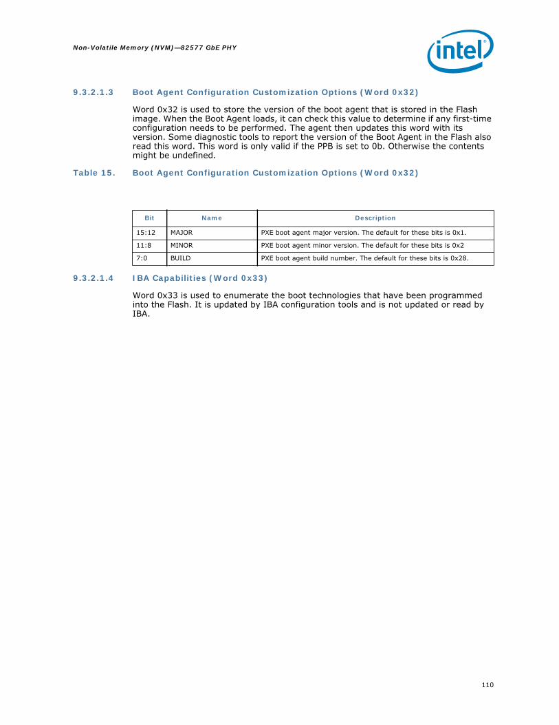
110
Non-Volatile Memory (NVM)—82577 GbE PHY
9.3.2.1.3 Boot Agent Configuration Customization Options (Word 0x32)
Word 0x32 is used to store the version of the boot agent that is stored in the Flash image. When the Boot Agent loads, it can check this value to determine if any first-time configuration needs to be performed. The agent then updates this word with its version. Some diagnostic tools to report the version of the Boot Agent in the Flash also read this word. This word is only valid if the PPB is set to 0b. Otherwise the contents might be undefined.
Table 15. Boot Agent Configuration Customization Options (Word 0x32)
9.3.2.1.4 IBA Capabilities (Word 0x33)
Word 0x33 is used to enumerate the boot technologies that have been programmed into the Flash. It is updated by IBA configuration tools and is not updated or read by IBA.
Bit Name Description
15:12 MAJOR PXE boot agent major version. The default for these bits is 0x1.
11:8 MINOR PXE boot agent minor version. The default for these bits is 0x2
7:0 BUILD PXE boot agent build number. The default for these bits is 0x28.

82577 GbE PHY—Non-Volatile Memory (NVM)
111
Table 16. IBA Capabilities
9.3.2.2 Checksum Word Calculation (Word 0x3F)
The Checksum word (Word 0x3F, NVM bytes 0x7E and 0x7F) is used to ensure that the base NVM image is a valid image. The value of this word should be calculated such that after adding all the words (0x00-0x3F) / bytes (0x00-0x7F), including the Checksum word itself, the sum should be 0xBABA. The initial value in the 16 bit summing register should be 0x0000 and the carry bit should be ignored after each addition.
Note: Hardware does not calculate the word 0x3F checksum during NVM write; it must be calculated by software independently and included in the NVM write data. Hardware does not compute a checksum over words 0x00-0x3F during NVM reads in order to determine validity of the NVM image; this field is provided strictly for software verification of NVM validity. All hardware configuration based on word 0x00-0x3F content is based on the validity of the Signature field of the NVM.
9.3.3 Basic Configuration Software WordsThis section describes the meaningful NVM words in the basic configuration space that are used by software at word addresses 0x03-0x09.
9.3.3.1 Reserved (Word 0x3)
Bit Name Description
15:14 SIGSignatureThese bits must be set to 01b to indicate that this word has been programmed by the agent or other configuration software.
13:5 Reserved Reserved, must be set to 0x00.
4 iSCSI boot capability not present (0b default).
3 EFIEFI EBC capability is present in Flash.0b = The EFI code is not present (default).1b = The EFI code is present.
2 Reserved Reserved, set to 1b.
1 UNDIPXE/UNDI capability is present in Flash.1b = The PXE base code is present (default).0b = The PXE base code is not present.
0 BCPXE base code is present in Flash.0b = The PXE base code is present (default).1b = The PXE base code is not present.
Bits Name Default Description
15:12 Reserved 0x0 Reserved, set to 0x0.
11 LOM 1bLOMSet to 1b.
10:0 Reserved 0x00 Reserved, set to 0x00.

112
Non-Volatile Memory (NVM)—82577 GbE PHY
9.3.3.2 Reserved (Words 0x04, 0x06, and 0x07)
9.3.3.3 Image Version Information (Word 0x05)
Note: This is a reserved word and cannot be changed.
Care should be taken to use the correct GbE NVM firmware revision for the stepping combination of the Intel® 5 Series Express Chipset and the 82577. The following table lists the NVM revision that is optimized for use with the silicon stepping combination.
Note: Using a newer revision NVM with an older silicon stepping or older revision NVM with a newer silicon stepping could cause system instability and unpredictable behavior.
9.3.3.4 PBA Low and PBA High (Words 0x08 and 0x09)
The nine-digit Printed Board Assembly (PBA) number used for Intel manufactured Network Interface Cards (NICs) and Lan on Motherboard (LOMs) are stored in a four-byte field. The dash itself is not stored, neither is the first digit of the 3-digit suffix, as it is always zero for the affected products. Note that through the course of hardware ECOs, the suffix field (byte 4) is incremented. The purpose of this information is to allow customer support (or any user) to identify the exact revision level of a product.
Note: Network driver software should not rely on this field to identify the product or its capabilities.
Example: PBA number = 123456-003 to Word 0x08 = 0x1234; Word 0x09 = 0x5603.
Bits Name Default Description
15:0 Reserved 0xFFFF Reserved
Intel® 5 Series Express Chipset
Stepping82577
Stepping/PHY-Ver LAN Switch NVM Version Comments
B1 A3
Yes 0.71 Design with LAN switch.
No but support dock 0.71/0.73
Design without LAN switch.
No and No support for dock 0.73
Bits Word Default Description
15:0 0x08 0xFFFF PBA low.
15:0 0x09 0xFFFF PBA high.

82577 GbE PHY—Non-Volatile Memory (NVM)
113
9.4 Intel® 5 Series Express Chipset/82577 NVM ContentsThis section lists the NVM contents for the Intel® 5 Series Express Chipset and the 82577.
Table 17. LAN NVM Contents
Word Description
0x00:0x02 Ethernet Individual Address
0x03:0x04 Reserved
0x05 Image Version Information
0x06:0x07 Reserved
0x08:0x09 PBA Bytes
0x0A PCI Init Control Word
0x0B Subsystem ID
0x0C Subsystem Vendor ID
0x0D Device ID
0x0E Reserved
0x0F Reserved
0x10 LAN Power Consumption
0x11 Reserved
0x12 Reserved
0x13 Shared Init Control Word
0x14:0x16 Extended Configuration Words
0x17 OEM Configuration Defaults
0x18 LED 0 - 2
0x19:0x2F Reserved
0x30:0x3E PXE Region
0x3F Software Checksum

114
Non-Volatile Memory (NVM)—82577 GbE PHY
Note: This page intentionally left blank.
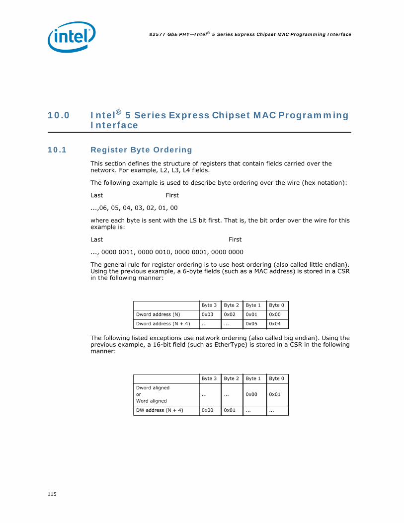
82577 GbE PHY—Intel® 5 Series Express Chipset MAC Programming Interface
115
10.0 Intel® 5 Series Express Chipset MAC Programming Interface
10.1 Register Byte OrderingThis section defines the structure of registers that contain fields carried over the network. For example, L2, L3, L4 fields.
The following example is used to describe byte ordering over the wire (hex notation):
Last First
...,06, 05, 04, 03, 02, 01, 00
where each byte is sent with the LS bit first. That is, the bit order over the wire for this example is:
Last First
..., 0000 0011, 0000 0010, 0000 0001, 0000 0000
The general rule for register ordering is to use host ordering (also called little endian). Using the previous example, a 6-byte fields (such as a MAC address) is stored in a CSR in the following manner:
The following listed exceptions use network ordering (also called big endian). Using the previous example, a 16-bit field (such as EtherType) is stored in a CSR in the following manner:
Byte 3 Byte 2 Byte 1 Byte 0
Dword address (N) 0x03 0x02 0x01 0x00
Dword address (N + 4) ... ... 0x05 0x04
Byte 3 Byte 2 Byte 1 Byte 0
Dword alignedorWord aligned
... ... 0x00 0x01
DW address (N + 4) 0x00 0x01 ... ...

116
Intel® 5 Series Express Chipset MAC Programming Interface—82577 GbE PHY
The following exceptions use network ordering:
• All ETherType fields
The normal notation as it appears in text books, etc. is to use network ordering. For example, the following MAC address: 00-A0-C9-00-00-00. The order on the network is 00, then A0, then C9, etc. However, the host ordering presentation would be:
10.2 Register ConventionsAll registers in the MAC are defined to be 32 bits, so write cycles should be accessed as 32 bit double-words, There are some exceptions to this rule:
• Register pairs where two 32-bit registers make up a larger logical size
Reserved bit positions: Some registers contain certain bits that are marked as reserved. These bits should never be set to a value of 1b by software. Reads from registers containing reserved bits might return indeterminate values in the reserved bit positions unless read values are explicitly stated. When read, these reserved bits should be ignored by software.
Reserved and/or undefined addresses: any register address not explicitly declared in this document should be considered to be reserved, and should not be written to. Writing to reserved or undefined register addresses might cause indeterminate behavior. Reads from reserved or undefined configuration register addresses might return indeterminate values unless read values are explicitly stated for specific addresses. Reserved fields within defined registers are defined as Read-Only (RO). When writing to these registers, the RO fields should be set to their initial value. Reading from reserved fields might return indeterminate values.
Initial values: most registers define the initial hardware values prior to being programmed. In some cases, hardware initial values are undefined and are listed as such via the text undefined, unknown, or X. Some of these configuration values might need to be set via NVM configuration or via software in order for proper operation to occur. Note that this need is dependent on the function of the bit. Other registers might cite a hardware default that is overridden by a higher-precedence operation. Operations that might supersede hardware defaults might also include a valid NVM load, completion of a hardware operation (such as hardware auto-negotiation), or writing of a different register whose value is then reflected in another bit.
For registers that should be accessed as 32-bit double words, partial writes (less than a 32-bit double word) does not take effect (the write is ignored). Partial reads return all 32 bits of data regardless of the byte enables.
Note: Partial reads to read-on-clear registers (such as ICR) can have unexpected results since all 32 bits are actually read regardless of the byte enables. Partial reads should not be done.
Note: All statistics registers are implemented as 32-bit registers. Though some logical statistics registers represent counters in excess of 32 bits in width, registers must be accessed using 32-bit operations (like independent access to each 32-bit field).
Byte 3 Byte 2 Byte 1 Byte 0
Dword address (N) 00 C9 A0 00
Dword address (N + 4) ... ... 00 00
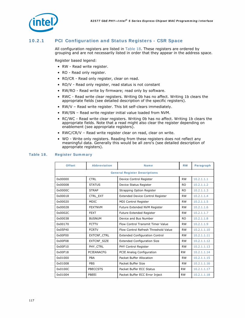
82577 GbE PHY—Intel® 5 Series Express Chipset MAC Programming Interface
117
10.2.1 PCI Configuration and Status Registers - CSR Space
All configuration registers are listed in Table 18. These registers are ordered by grouping and are not necessarily listed in order that they appear in the address space.
Register based legend:• RW - Read write register.• RO - Read only register.• RO/CR - Read only register, clear on read.• RO/V - Read only register, read status is not constant• RW/RO - Read write by firmware; read only by software.• RWC - Read write clear registers. Writing 0b has no affect. Writing 1b clears the
appropriate fields (see detailed description of the specific registers).• RW/V – Read write register. This bit self-clears immediately.• RW/SN – Read write register initial value loaded from NVM.• RC/WC - Read write clear registers. Writing 0b has no affect. Writing 1b clears the
appropriate fields. Note that a read might also clear the register depending on enablement (see appropriate registers).
• RWC/CR/V – Read write register clear on read, clear on write.• WO - Write only registers. Reading from these registers does not reflect any
meaningful data. Generally this would be all zero's (see detailed description of appropriate registers).
Table 18. Register Summary
Offset Abbreviation Name RW Paragraph
General Register Descriptions
0x00000 CTRL Device Control Register RW 10.2.1.1.1
0x00008 STATUS Device Status Register RO 10.2.1.1.2
0x0000C STRAP Strapping Option Register RO 10.2.1.1.3
0x00018 CTRL_EXT Extended Device Control Register RW 10.2.1.1.4
0x00020 MDIC MDI Control Register RW 10.2.1.1.5
0x00028 FEXTNVM Future Extended NVM Register RW 10.2.1.1.6
0x0002C FEXT Future Extended Register RW 10.2.1.1.7
0x00038 BUSNUM Device and Bus Number RO 10.2.1.1.8
0x00170 FCTTV Flow Control Transmit Timer Value RW 10.2.1.1.9
0x05F40 FCRTV Flow Control Refresh Threshold Value RW 10.2.1.1.10
0x00F00 EXTCNF_CTRL Extended Configuration Control RW 10.2.1.1.11
0x00F08 EXTCNF_SIZE Extended Configuration Size RW 10.2.1.1.12
0x00F10 PHY_CTRL PHY Control Register RW 10.2.1.1.13
0x00F18 PCIEANACFG PCIE Analog Configuration RW 10.2.1.1.14
0x01000 PBA Packet Buffer Allocation RW 10.2.1.1.15
0x01008 PBS Packet Buffer Size RW 10.2.1.1.16
0x0100C PBECCSTS Packet Buffer ECC Status RW 10.2.1.1.17
0x01004 PBEEI Packet Buffer ECC Error Inject RW 10.2.1.1.18

118
Intel® 5 Series Express Chipset MAC Programming Interface—82577 GbE PHY
Interrupt Register Descriptions
0x000C0 ICR Interrupt Cause Read Register RC/WC 10.2.1.2.1
0x000C4 ITR Interrupt Throttling Register RW 10.2.1.2.2
0x000C8 ICS Interrupt Cause Set Register WO 10.2.1.2.3
0x000D0 IMS Interrupt Mask Set/Read Register RW 10.2.1.2.4
0x000D8 IMC Interrupt Mask Clear Register WO 10.2.1.2.5
0x000E0 Mask - IAM Interrupt Acknowledge Auto RW 10.2.1.2.6
Receive Register Descriptions
0x00100 RCTL Receive Control Register RW 10.2.1.3.1
0x00104 RCTL1 Receive Control Register 1 RW 10.2.1.3.2
0x02008 ERT Early Receive Threshold RW 10.2.1.3.3
0x02170 PSRCTL Packet Split Receive Control Register RW 10.2.1.3.4
0x02160 FCRTL Flow Control Receive Threshold Low RW 10.2.1.3.5
0x02168 FCRTH Flow Control Receive Threshold High RW 10.2.1.3.6
0x02800 RDBAL Receive Descriptor Base Address Low Queue RW 10.2.1.3.7
0x02804 RDBAH Receive Descriptor Base Address High Queue RW 10.2.1.3.8
0x02808 RDLEN Receive Descriptor Length Queue RW 10.2.1.3.9
0x02810 RDH Receive Descriptor Head Queue RW 10.2.1.3.10
0x02818 RDT Receive Descriptor Tail Queue RW 10.2.1.3.11
0x02820 RDTR Interrupt Delay Timer (Packet Timer) RW 10.2.1.3.12
0x02828 RXDCTL Receive Descriptor Control RW 10.2.1.3.13
0x0282C RADV Receive Interrupt Absolute Delay Timer RW 10.2.1.3.14
0x02C00 RSRPD Receive Small Packet Detect Interrupt RW 10.2.1.3.15
0x02C08 RAID Receive ACK Interrupt Delay Register RW 10.2.1.3.16
0x05000 RXCSUM Receive Checksum Control RW 10.2.1.3.17
0x05008 RFCTL Receive Filter Control Register RW 10.2.1.3.18
0x05200-0x0527C MTA[31:0] Multicast Table Array RW 10.2.1.3.19
0x05400 + 8*n (n=0…6) RAL Receive Address Low RW 10.2.1.3.20
0x05404 + 8*n (n=0…6) RAH Receive Address High RW 10.2.1.3.21
0x05438 + 8*n (n=0…3) SRAL Shared Receive Address Low RW 10.2.1.3.22
0x0543C + 8*n (n=0…2) SRAH Shared Receive Address High 0…2 RW 10.2.1.3.23
0x05454 SHRAH[3] Shared Receive Address High 3 RW 10.2.1.3.24
0x05818 MRQC Multiple Receive Queues Command Register RW 10.2.1.3.25
0x05C00 + 4*n (n=0…31) RETA Redirection Table RW 10.2.1.3.26
0x05C80 + 4*n (n=0…9) RSSRK Random Key Register RW 10.2.1.3.27
Offset Abbreviation Name RW Paragraph
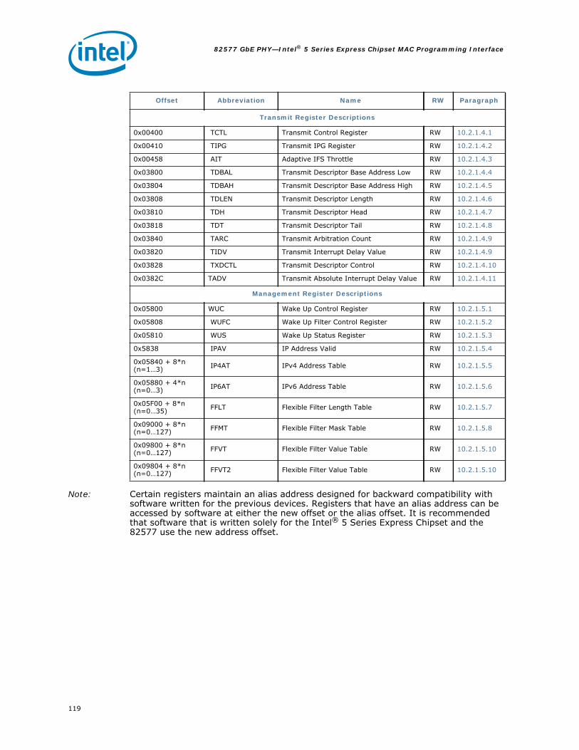
82577 GbE PHY—Intel® 5 Series Express Chipset MAC Programming Interface
119
Note: Certain registers maintain an alias address designed for backward compatibility with software written for the previous devices. Registers that have an alias address can be accessed by software at either the new offset or the alias offset. It is recommended that software that is written solely for the Intel® 5 Series Express Chipset and the 82577 use the new address offset.
Transmit Register Descriptions
0x00400 TCTL Transmit Control Register RW 10.2.1.4.1
0x00410 TIPG Transmit IPG Register RW 10.2.1.4.2
0x00458 AIT Adaptive IFS Throttle RW 10.2.1.4.3
0x03800 TDBAL Transmit Descriptor Base Address Low RW 10.2.1.4.4
0x03804 TDBAH Transmit Descriptor Base Address High RW 10.2.1.4.5
0x03808 TDLEN Transmit Descriptor Length RW 10.2.1.4.6
0x03810 TDH Transmit Descriptor Head RW 10.2.1.4.7
0x03818 TDT Transmit Descriptor Tail RW 10.2.1.4.8
0x03840 TARC Transmit Arbitration Count RW 10.2.1.4.9
0x03820 TIDV Transmit Interrupt Delay Value RW 10.2.1.4.9
0x03828 TXDCTL Transmit Descriptor Control RW 10.2.1.4.10
0x0382C TADV Transmit Absolute Interrupt Delay Value RW 10.2.1.4.11
Management Register Descriptions
0x05800 WUC Wake Up Control Register RW 10.2.1.5.1
0x05808 WUFC Wake Up Filter Control Register RW 10.2.1.5.2
0x05810 WUS Wake Up Status Register RW 10.2.1.5.3
0x5838 IPAV IP Address Valid RW 10.2.1.5.4
0x05840 + 8*n (n=1…3) IP4AT IPv4 Address Table RW 10.2.1.5.5
0x05880 + 4*n (n=0…3) IP6AT IPv6 Address Table RW 10.2.1.5.6
0x05F00 + 8*n (n=0…35) FFLT Flexible Filter Length Table RW 10.2.1.5.7
0x09000 + 8*n (n=0…127) FFMT Flexible Filter Mask Table RW 10.2.1.5.8
0x09800 + 8*n (n=0…127) FFVT Flexible Filter Value Table RW 10.2.1.5.10
0x09804 + 8*n (n=0…127) FFVT2 Flexible Filter Value Table RW 10.2.1.5.10
Offset Abbreviation Name RW Paragraph

120
Intel® 5 Series Express Chipset MAC Programming Interface—82577 GbE PHY
10.2.1.1 General Register Descriptions
10.2.1.1.1 Device Control Register - CTRL (0x00000; RW)
Bit Type Reset Description
0 RW/SN 1b
Full Duplex (FD).0b = Half duplex.1b = Full duplex. Controls the MAC duplex setting when explicitly set by software. Loaded from the NVM word 0x13.
1 RO 0b Reserved. Write as 0b for future compatibility
2 RW 0bMaster Disable. When set, the MAC blocks new master requests on the PCI device. Once no master requests are pending by this function, the Master Enable Status bit is cleared.
5:3 RO 000b Reserved. Write as 0b for future compatibility.
6 RO 1b Reserved.
7 RO 0b Reserved. Must be set to 0b.
9:8 RW 10b
Speed selection (SPEED). These bits might determine the speed configuration and are written by software after reading the PHY configuration through the MDIO interface. These signals are ignored when auto-speed detection is enabled.0)b = 10 Mb/s.0)b = 100 Mb/s.10b = 1000 Mb/s.11b = Not used.
10 RO 0b Reserved. Write as 0b for future compatibility.
11 RW/SN 0b
Force Speed (FRCSPD). This bit is set when software needs to manually configure the MAC speed settings according to the Speed bits (bits 9:8). When using the 82577, note that it must resolve to the same speed configuration or software must manually set it to the same speed as the MAC. The value is loaded from word 0x13 in the NVM. Note that this bit is superseded by the CTRL_EXT.SPD_BYPS bit, which has a similar function.
12 RW 0b
Force Duplex (FRCDPLX). When set to 1b, software might override the duplex indication from the 82577 that is indicated in the FDX to the MAC. Otherwise, the duplex setting is sampled from the 82577 FDX indication into the MAC on the asserting edge of the PHY link signal. When asserted, the CTRL.FD bit sets duplex.
13 RO 0b Reserved.
14 RW/SN 0b Reserved.
15 RO 0b Reserved. Reads as 0.
18:16 RW 0b0 Reserved.
19 RW 0bMemory Error Handling Enable (MEHE). When set to 1b, the Intel® 5 Series Express Chipset reaction to correctable and uncorrectable memory errors detection are activated.
20 1b Reserved.
24:21 RO 0x0 Reserved.
25 RW 0b Reserved.
26 RW/V 0bHost Software Reset (SWRST). This bit performs a reset to the PCI data path and the relevant shared logic. Writing 1b initiates the reset. This bit is self-clearing.
27 RW 0bReceive Flow Control Enable (RFCE). Indicates that the MAC responds to receiving flow control packets. If auto-negotiation is enabled, this bit is set to the negotiated duplex value.

82577 GbE PHY—Intel® 5 Series Express Chipset MAC Programming Interface
121
Note: Fields loaded from the NVM are set by the NVM only if the signature bits of the NVM's Initialization Control Word match 01b.
This register, as well as the Extended Device Control register (CTRL_EXT), controls the major operational modes for the MAC. While software writes to this register to control MAC settings, several bits (such as FD and SPEED) might be overridden depending on other bit settings and the resultant link configuration is determined by the 82577's auto-negotiation resolution.
The FD (duplex) and SPEED configurations of the MAC are normally determined from the link configuration process. Software might specifically override/set these MAC settings via certain bits in a forced-link scenario; if so, the values used to configure the MAC must be consistent with the 82577 settings.
Manual link configuration is controlled through the 82577's MII management interface.
Host Software Reset (bit 26), might be used to globally reset the entire host data path and shared logic. This register is provided primarily as a last-ditch software mechanism to recover from an indeterminate or suspected hung hardware state. Most registers (receive, transmit, interrupt, statistics, etc.), and state machines are set to their power-on reset values, approximating the state following a power-on or PCI reset. One internal configuration register, the Packet Buffer Allocation (PBA) register, retains its value through a software reset.
Note: To ensure that the global device reset has fully completed and that the MAC responds to subsequent accesses, programmers must wait approximately 1 ms after setting before attempting to check to see if the bit has cleared or to access (read or write) any other device register.
Note: This register's address is also reflected at address 0x00004 for legacy reasons. Neither the software driver nor firmware should use it since it might be unsupported in next generations.
Bit Type Reset Description
28 RW 0bTransmit Flow Control Enable (TFCE). Indicates that the MAC transmits flow control packets (XON and XOFF frames) based on receiver fullness. If auto-negotiation is enabled, this bit is set to the negotiated duplex value.
29 RO 0b Reserved.
30 RW 0b
VLAN Mode Enable (VME). When set to 1b, all packets transmitted from MAC that have VLE set is sent with an 802.1Q header added to the packet. The contents of the header come from the transmit descriptor and from the VLAN type register. On receive, VLAN information is stripped from 802.1Q packets.
31 RW/V 0b
LAN Connected Device Reset (LCD_RST). Controls an inband message to the 82577.0b = Normal operation1b = Reset to PHY is asserted.The LCD_RST functionality is gated by the FWSM.RSPCIPHY bit. If the FWSM.RSPCIPHY bit is not set to 1b, then setting the LCD_RST has no impact. For proper operation, software or firmware must also set the SWRST bit in the register at the same time. This bit is self-clearing.

122
Intel® 5 Series Express Chipset MAC Programming Interface—82577 GbE PHY
10.2.1.1.2 Device Status Register - STATUS (0x00008; RO)
Bits Attribute Reset Description
0 RO/V X
Full Duplex (FD).0b = Half duplex.1b = Full duplex.Reflects duplex setting of the MAC and/or link.
1 RO/V X
Link up (LU). 0b = No link established.1b = Link established.For this to be valid, the Set Link Up bit of the Device Control register (CTRL.SU) must be set.
3:2 RO/V 00b
PHY Type Indication (PHYTYPE). Indicates that the 82577 attached to the MAC and resulted mode of operation of the MAC/82577 Link buses.00 = 82577.01 =Reserved.10 = Reserved.11 = Reserved.This field is loaded from the Shared Init control word in the NVM.
4 RO/V X Transmission Paused (TXOFF). Indication of pause state of the transmit function when symmetrical flow control is enabled.
5 RO/V 1b
PHY Power Up not (PHYPWR). RO bit that indicates the power state of the 82577.0b = The 82577 is powered on in the active state.1b = The 82577 is in the power down state.The PHYPWR bit is valid only after PHY reset is asserted. Note: The PHY power up indication reflects the status of the LANPHYPC signaling to the 82577.
7:6 RO/V X
Link speed setting (SPEED). This bit reflects the speed setting of the MAC and/or link.00b = 10 Mb/s.01b = 100 Mb/s.10b = 1000 Mb/s.11b = 1000 Mb/s.
8 RO/V XMaster Read Completions Blocked. This bit is set when the MAC receives a completion with an error (EP = one or status!= successful).It is cleared on PCI reset.
9 RW/V/C 0b
LAN Init Done. This bit is asserted following completion of the LAN initialization from the Flash.Software is expected to clear this field to make it usable for the next initialization done event.
10 RW/V/C 1bPHY Reset Asserted (PHYRA). This bit is R/W. Hardware sets this bit following the assertion of a 82577 reset (either hardware or in-band). The bit is cleared on writing 0b to it.
18:11 RO 0x0 Reserved.
19 RO/V 1b
Master Enable Status. Cleared by the MAC when the Master Disable bit is set and no master requests are pending by this function, otherwise this bit is set. This bit indicates that no master requests are issued by this function as long as the Master Disable bit is set.
29:20 RO 0x0 Reserved. Reads as 0.
30 RO 0b Reserved.
31 RO/SN 1bClock Control ¼ (CLK_CNT_1_4). This bit is loaded from the NVM word 0x13 and indicates the MAC supports lowering its DMA clock to ¼ of its value.

82577 GbE PHY—Intel® 5 Series Express Chipset MAC Programming Interface
123
FD reflects the actual MAC duplex configuration. This normally reflects the duplex setting for the entire link, as it normally reflects the duplex configuration negotiated between the PHY and link partner (copper link) or MAC and link partner (fiber link).
Link up provides a useful indication of whether something is attached to the port. Successful negotiation of features/link parameters results in link activity. The link startup process (and consequently the duration for this activity after reset) might be several 100's of ms. It reflects whether the PHY's link indication is present.
TXOFF indicates the state of the transmit function when symmetrical flow control has been enabled and negotiated with the link partner. This bit is set to 1b when transmission is paused due to the reception of an XOFF frame. It is cleared upon expiration of the pause timer or the receipt of an XON frame.
SPEED indicates the actual MAC speed configuration. These bits normally reflect the speed of the actual link, negotiated by the PHY and link partner, and reflected internally from the PHY to the MAC. These bits might represent the speed configuration of the MAC only, if the MAC speed setting has been forced via software (CTRL.SPEED). Speed indications are mapped as shown below:
• 00b = 10 Mb/s• 01b = 100 Mb/s• 10b = 1000 Mb/s• 11b = 1000 Mb/s

124
Intel® 5 Series Express Chipset MAC Programming Interface—82577 GbE PHY
10.2.1.1.3 Strapping Option Register - STRAP (0x0000C; RO)
This register reflects the values of the soft strapping options fetched from the NVM descriptor in the Intel® 5 Series Express Chipset space. These signals are sampled by the MAC following LAN_RST# or global reset (PCI reset assertion).
10.2.1.1.4 Extended Device Control Register - CTRL_EXT (0x00018; RW)
Bit(s) Type Reset Description
0 RO 1b Reserved.
5:1 RO 0x0LAN NVM Size (NVMS). LAN NVM space size is indicated in multiples of 4 KB. LAN NVM size might very from 4 KB to 128 KB (a zero value means 4 KB).
10:6 RO 0x0 Reserved.
15:11 RO 0x0 Reserved.
16 RO 0b MAC SMBus address enable (LCSMBADDEN).
23:17 RO 0x0 MAC SMBus address (LCSMBADD).
24 RO 0b PHY SMBus address enable (LCDSMBADDEN).
31:25 RO 0x0 PHY SMBus address (LCDSMBADD).
Bits Type Reset Description
11:0 RO 0x0 Reserved.
12 RW/V 1b Reserved.
14:13 00b Reserved.
15 RW 0b
Speed Select Bypass (SPD_BYPS). When set to 1, all speed detection mechanisms are bypassed, and the device is immediately set to the speed indicated by CTRL.SPEED. This provides a method for software to have full control of the speed settings of the device when the change takes place by overriding hardware clock switching circuitry.
18:16 000b Reserved.
19 RW/SN 0bDynamic Clock Gating (DynCK). When set, this bit enables dynamic clock gating of the DMA and MAC units. Refer to the description of the DynWakeCK in this register. This bit is loaded from NVM word 0x13.
20 RW/SN 1bPHY Power Down Enable (PHYPDEN). When set, this bit enables the 82577 to enter a low-power state when the MAC is at the DMoff / D3 or Dr with no WoL. This bit is loaded from word 0x13 in the NVM.
24:21 0000b Reserved.
25 RW 0b
DMA Clock Control (DMACKCTL). Controls the DMA clock source in non- GbE mode (10/100 and no Link). In GbE mode, the DMA clock source is always GLCI PLL divided by two. In normal operation, this bit should be in the default state in which the DMA clock source in non-GbE is mosc_clk.In test mode the DMACKCTL and PLLGateDis should be set to 1b and CLK_CNT_1_4 in the NVM should not be set. In this mode, the DMA clock source is GLCI PLL divided by two.
26 RW 0b
Disable Static GLCI PLL Gating (PLLGateDis). By default the PLL is functional only when the GLCI link is required, and inactive when it is not required (at non-GbE mode if LCI is available). When set to 1b the GLCI PLL is always active.
27 RW 0b
Interrupt Acknowledge Auto-Mask Enable (IAME). When this bit is set, a read or write to the ICR register has the side effect of writing the value in the IAM register to the IMC register. When this bit is 0b, this feature is disabled.

82577 GbE PHY—Intel® 5 Series Express Chipset MAC Programming Interface
125
This register provides extended control of device functionality beyond that provided by the Device Control (CTRL) register.
Note: If software uses the EE_RST function and needs to retain current configuration information, the contents of the control registers should be read and stored by software. Control register values are changed by a read of the NVM, which occurs after asserting the EE_RST bit.
Note: The EEPROM reset function might read configuration information out of the NVM, which affects the configuration of PCI configuration space BAR settings. The changes to the BAR's are not visible unless the system is rebooted and the BIOS is allowed to re-map them.
Note: The SPD_BYPS bit performs a similar function as the CTRL.FRCSPD bit in that the device's speed settings are determined by the value software writes to the CRTL.SPEED bits. However, with the SPD_BYPS bit asserted, the settings in CTRL.SPEED take effect immediately rather than waiting until after the device's clock switching circuitry performs the change.
Bits Type Reset Description
28 RW 0b
Driver loaded (DRV_LOAD). This bit should be set by the driver after it was loaded and cleared when the driver unloads or after a soft reset. The Manageability Controller (MC) loads this bit to indicate that the driver has loaded.
29 RW 0b
INT_TIMERS_CLEAR_ENA. When set, this bit enables the clear of the interrupt timers following an IMS clear. In this state, successive interrupts occur only after the timers expire again. When cleared, successive interrupts following IMS clear might happen immediately.
30 0b Reserved.
31 RO 0b Reserved. Reads as 0.

126
Intel® 5 Series Express Chipset MAC Programming Interface—82577 GbE PHY
10.2.1.1.5 MDI Control Register - MDIC (0x00020; RW)
This register is used by software to read or write Management Data Interface (MDI) registers in the 82577.
Note: Internal logic uses MDIC to communicate with the 82577. All fields in these registers are indicated as "/V" since the internal logic might use them to access the 82577. Since hardware uses this register, all hardware, software and firmware must use semaphore logic (the ownership flags) before accessing the MDIC.
For an MDI read cycle the sequence of events is as follows:
1. The CPU performs a write cycle to the MII register with:— Ready = 0b— Interrupt Enable bit set to 1b or 0b— Op-Code = 10b (read)— PHYADD = The 82577 address from the MDI register— REGADD = The register address of the specific register to be accessed (0
through 31)2. The MAC applies the following sequence on the MDIO signal to the 82577:
— <PREAMBLE><01><10><PHYADD><REGADD><Z>
where the Z stands for the MAC tri-stating the MDIO signal.
3. The 82577 returns the following sequence on the MDIO signal:— <0><DATA><IDLE>
4. The MAC discards the leading bit and places the following 16 data bits in the MII register.
5. The MAC asserts an Interrupt indicating MDI done, if the Interrupt Enable bit was set.
6. The MAC sets the Ready bit in the MII register indicating the read is complete.
Bits Type Reset Description
15:0 RW/V X
Data (DATA). In a Write command, software places the data bits and the MAC shifts them out to the 82577. In a Read command, the MAC reads these bits serially from the 82577 and software can read them from this location.
20:16 RW/V 0x0 PHY Register address (REGADD). For example, register 0, 1, 2, … 31.
25:21 RW/V 0x0 PHY Address (PHYADD).
27:26 RW/V 00b
Op-code (OP). 01b = MDI write.10b = MDI read. Other values are reserved.
28 RW/V 1bReady bit (R). Set to 1b by the MAC at the end of the MDI transaction (for example, indicates a read or write completed). It should be reset to 0b by software at the same time the command is written.
29 RW/V 0b Interrupt Enable (I). When set to 1b by software, it causes an interrupt to be asserted to indicate the end of an MDI cycle.
30 RW/V 0bError (E). This bit set is to 1b by hardware when it fails to complete an MDI read. Software should make sure this bit is clear (0b) before making a MDI read or write command.
31 RO 0b Reserved. Write as 0b for future compatibility.

82577 GbE PHY—Intel® 5 Series Express Chipset MAC Programming Interface
127
7. The CPU might read the data from the MII register and issue a new MDI command.
For an MDI Write cycle the sequence of events is as follows:
1. The CPU performs a write cycle to the MII register with:— Ready = 0b— Interrupt Enable bit set to 1b or 0b— Op-Code = 01b (write)— PHYADD = The 82577 address from the MDI register— REGADD = The register address of the specific register to be accessed (0
through 31)— Data = specific data for desired control of the 82577
2. The MAC applies the following sequence on the MDIO signal to the 82577:— <PREAMBLE><01><01><PHYADD><REGADD><10><DATA><IDLE>
3. The MAC asserts an Interrupt indicating MDI done if the Interrupt Enable bit was set.
4. The MAC sets the Ready bit in the MII register to indicate step 2 has been completed.
5. The CPU might issue a new MDI command.
Note: An MDI read or write might take as long as 64 ms from the CPU write to the Ready bit assertion.
If an invalid opcode is written by software, the MAC does not execute any accesses to the 82577 registers.
If the 82577 does not generate a zero as the second bit of the turnaround cycle for reads, the MAC aborts the access, sets the E (error) bit, writes 0xFFFF to the data field to indicate an error condition, and sets the ready bit.
10.2.1.1.6 Future Extended NVM Register - FEXTNVM (0x00028; RW)
This register is initialized to a hardware default only at LAN_RST# reset. Software should not modify these fields to values other than their recommended values. Bits 15:0 of this register are loaded from the NVM word 0s19 and bits 31:16 are loaded from the NVM word 0x1A.
Bits Type Reset Description
0 RW/SN 0b Reserved
1 RW/SN 0b dma_clk_enable_d. Enable dynamic clock stop. When this bit is set to 1b, clk is always ticking. The default value is 0b (hardware and NVM).
2 RW/SN 0b wake_dma_clk_enable_d. Enable dynamic clock stop. When this bit is set to 1b, clk is always ticking. The default value is 0b (hardware and NVM)
3 RW/SN 0b gpt_clk_enable_d. Enable dynamic clock stop. When this bit is set to 1b, clk is always ticking. The default value is 0b (hardware and NVM)
4 RW/SN 0b mac_clk_enable_d. Enable dynamic clock stop. When this bit is set to 1b, clk is always ticking. The default value is 0b (hardware and NVM)
5 RW/SN 0b m2k_clk_enable_d. Enable dynamic clock stop. When this bit is set to 1b, clk is always ticking. The default value is 0b (hardware and NVM).
6 RW/SN 0bInvalid Image CSUM. When cleared, this bit indicates to the Intel NVM programming tools that the image CSUM needs to be corrected. When set the CSUM is assumed to be correct.
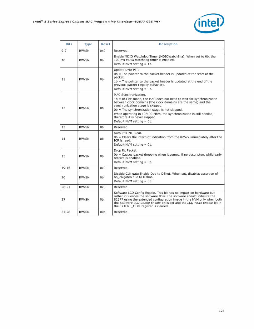
128
Intel® 5 Series Express Chipset MAC Programming Interface—82577 GbE PHY
9:7 RW/SN 0x0 Reserved.
10 RW/SN 0bEnable MDIO Watchdog Timer (MDIOWatchEna). When set to 0b, the 100 ms MDIO watchdog timer is enabled.Default NVM setting = 1b.
11 RW/SN 0b
Update DMA PTR.0b = The pointer to the packet header is updated at the start of the packet.1b = The pointer to the packet header is updated at the end of the previous packet (legacy behavior).Default NVM setting = 0b.
12 RW/SN 0b
MAC Synchronization.1b = In GbE mode, the MAC does not need to wait for synchronization between clock domains (the clock domains are the same) and the synchronization stage is skipped.0b = The synchronization stage is not skipped.When operating in 10/100 Mb/s, the synchronization is still needed, therefore it is never skipped.Default NVM setting = 0b.
13 RW/SN 0b Reserved.
14 RW/SN 0b
Auto PHYINT Clear.0b = Clears the interrupt indication from the 82577 immediately after the ICR is read.Default NVM setting = 0b.
15 RW/SN 0b
Drop Rx Packet.0b = Causes packet dropping when it comes, if no descriptors while early receive is enabled.Default NVM setting = 0b.
19:16 RW/SN 0x0 Reserved.
20 RW/SN 0bDisable CLK gate Enable Due to D3hot. When set, disables assertion of bb_clkgaten due to D3hot.Default NVM setting = 0b.
26:21 RW/SN 0x0 Reserved.
27 RW/SN 0b
Software LCD Config Enable. This bit has no impact on hardware but rather influences the software flow. The software should initialize the 82577 using the extended configuration image in the NVM only when both the Software LCD Config Enable bit is set and the LCD Write Enable bit in the EXTCNF_CTRL register is cleared.
31:28 RW/SN 00b Reserved.
Bits Type Reset Description

82577 GbE PHY—Intel® 5 Series Express Chipset MAC Programming Interface
129
10.2.1.1.7 Future Extended Register - FEXT (0x0002C; RW)
This register is initialized to a hardware default only at LAN_RST# reset. Software should not modify these fields to values other than their recommended values.
C
10.2.1.1.8 Device and Bus Number - BUSNUM (0x00038; RO)
10.2.1.1.9 Flow Control Transmit Timer Value - FCTTV (0x00170; RW)
Bits Type Reset Description
0 0b Reserved.
1 RO 0b Reserved.
3:2 RO/V 00b Reserved.
7:4 RW 0x0 Reserved.
8 RW 0b
Hardware/Software CRC Mismatch Trigger. When set to 1b the MAC generates a trigger signal each time there is a mismatch between the software calculated CRC and hardware calculated CRC.This feature is ignored when CRC calculation is off-loaded to hardware.
9 RW 0b
Write Disable Ghost and DMA RAMs on CRC Mismatch. When set to 1b, disables any writes to the following RAMs in the event of CRC mismatch until reset:• Ghost read PCI descriptor• Ghost read PCI data• The four RAMs in the descriptor engine• The packet buffer
10 RW 0b When set to 1b, enables the data visibility of the ghost read PCI descriptor and PCI data RAMs to the NOA.
11 RW 0bVisibility in/out read data select. 1b = in.Bit 10 of the FEXT register must be set to 1b.
12 RW 0bVisibility data/desc read Ram select. 1b = data.Bit 10 of the FEXT register must be set to 1b.
13 RW 0b When set to 1b, the ghost read RAMs are readable by the slave bus.
17:14 RW 0x0 Must be set to 0x0.
31:18 RW 0x0 Future Extended. Reserved for future setting.
Bit Type Reset Description
7:0 RO 0x0 Reserved.
10:8 RO 000b Function Number. The MAC is a single PCI function being function 0.
15:11 RO 0x19 Device Number. During normal operation, the MAC has a pre-defined device number equal to 25 (0x19).
23:16 RO 0x0Bus Number. The MAC captures its bus number during host configuration write cycles type 0 aimed at the device. This field is initialized by LAN_RST# reset, PCI reset, and D3 to D0 transition.
31:24 RO 0x0 Reserved.
Bit Type Reset Description
15:0 RW XTransmit Timer Value (TTV). Included in XOFF frame.
31:16 RO 0x0 Reserved. Read as 0b. Should be written to 0b for future compatibility.

130
Intel® 5 Series Express Chipset MAC Programming Interface—82577 GbE PHY
The 16-bit value in the TTV field is inserted into a transmitted frame (either XOFF frames or any PAUSE frame value in any software transmitted packets). It counts in units of slot time. If software needs to send an XON frame, it must set TTV to zero prior to initiating the PAUSE frame.
Note: The MAC uses a fixed slot time value of 64 byte times.
10.2.1.1.10 Flow Control Refresh Threshold Value - FCRTV (0x05F40; RW)
10.2.1.1.11 Extended Configuration Control - EXTCNF_CTRL (0x00F00; RW)
Bit Type Reset Description
15:0 RW X
Flow Control Refresh Threshold (FCRT). This value indicates the threshold value of the flow control shadow counter. When the counter reaches this value, and the conditions for a pause state are still valid (buffer fullness above low threshold value), a pause (XOFF) frame is sent to the link partner.The FCRTV timer count interval is the same as other flow control timers and counts at slot times of 64 byte times. If this field contains a zero value, the flow control refresh is disabled.
31:16 RO 0x0 Reserved. Read as 0b. Should be written to 0b for future compatibility.
Bit Type Reset Description
0 RW/SN 0bLCD Write Enable. When set, enables the extended PHY configuration area in the MAC. When disabled, the extended PHY configuration area is ignored. Loaded from NVM word 0x14.
2:1 RW/SN 00b Reserved
3 RW/SN 1b OEM Write Enable. When set, enables auto load of the OEM bits from the PHY_CTRL register to the PHY. Loaded from NVM word 0x14.
4 RO 0b Reserved.
5 RW/V 0b
Software Semaphore FLAG (SWFLAG). This bit is set by the device driver to gain access permission to shared CSR registers with the firmware and hardware.The bit is initialized on power up PCI reset and software reset.
6 RO/V 0b MDIO Hardware Ownership. Hardware requests access to MDIO. Part of the arbitration scheme for MDIO access. This is a RO bit.
15:7 RO 0x0 Reserved.
27:16 RW/SN 0x001 Extended Configuration Pointer. Defines the base address (in Dwords) of the extended configuration area in the NVM.
31:28 RW 0b Reserved.
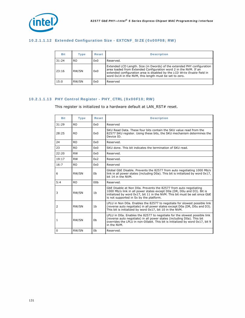
82577 GbE PHY—Intel® 5 Series Express Chipset MAC Programming Interface
131
10.2.1.1.12 Extended Configuration Size - EXTCNF_SIZE (0x00F08; RW)
10.2.1.1.13 PHY Control Register - PHY_CTRL (0x00F10; RW)
This register is initialized to a hardware default at LAN_RST# reset.
Bit Type Reset Description
31:24 RO 0x0 Reserved.
23:16 RW/SN 0x0
Extended LCD Length. Size (in Dwords) of the extended PHY configuration area loaded from Extended Configuration word 2 in the NVM. If an extended configuration area is disabled by the LCD Write Enable field in word 0x14 in the NVM, this length must be set to zero.
15:0 RW/SN 0x0 Reserved
Bit Type Reset Description
31:29 RO 0x0 Reserved
28:25 RO 0x0SKU Read Data. These four bits contain the SKU value read from the 82577 SKU register. Using these bits, the SKU mechanism determines the Device ID.
24 RO 0x0 Reserved.
23 RO 0x0 SKU done. This bit indicates the termination of SKU read.
22:20 RW 0x0 Reserved.
19:17 RW 0x2 Reserved.
16:7 RO 0x0 Reserved
6 RW/SN 0bGlobal GbE Disable. Prevents the 82577 from auto negotiating 1000 Mb/s link in all power states (including D0a). This bit is initialized by word 0x17, bit 14 in the NVM.
5:4 RO 00b Reserved.
3 RW/SN 1b
GbE Disable at Non D0a. Prevents the 82577 from auto negotiating 1000 Mb/s link in all power states except D0a (DR, D0u and D3). Bit is initialized by word 0x17, bit 11 in the NVM. This bit must be set since GbE is not supported in Sx by the platform.
2 RW/SN 1bLPLU in Non D0a. Enables the 82577 to negotiate for slowest possible link (reverse auto negotiate) in all power states except D0a (DR, D0u and D3). This bit is initialized by word 0x17, bit 10 in the NVM.
1 RW/SN 0b
LPLU in D0a. Enables the 82577 to negotiate for the slowest possible link (reverse auto negotiate) in all power states (including D0a). This bit overrides the LPLU in non-D0abit. This bit is initialized by word 0x17, bit 9 in the NVM.
0 RW/SN 0b Reserved.

132
Intel® 5 Series Express Chipset MAC Programming Interface—82577 GbE PHY
10.2.1.1.14 PCIE Analog Configuration - PCIEANACFG (0x00F18; RW)
10.2.1.1.15 Packet Buffer Allocation - PBA (0x01000; RW)
This register sets the on-chip receive and transmit storage allocation ratio.
Note: Programming this register does not automatically re-load or initialize internal packet-buffer RAM pointers. Software must reset both transmit and receive operation (using the global device reset CTRL.SWRST bit) after changing this register in order for it to take effect. The PBA register itself is not reset by assertion of the software reset, but is only reset upon initial hardware power on.
Note: If early receive functionality is not enabled (indicate field/register), the receive packet buffer should be larger than the maximum expected received packet + 32 bytes.
Note: For best performance, the transmit buffer allocation should be set to accept two full-sized packets.
Note: Transmit packet buffer size should be configured to be more than 4 KB.
10.2.1.1.16 Packet Buffer Size - PBS (0x01008; RW)
Bit Type Reset Description
0 RW 0b Invert Polarity. Indicates to the GP unit to invert bit polarity (only receiver). this bit is set from the NVM.
6:1 RW 0x20 Command Mode Voltage Select.
31:7 RO 0x0 Reserved. Read as 0b ignore on write.
Bit Type Reset Description
4:0 RW 0x Receive packet buffer allocation (RXA). Defines the size of the Rx buffer in K byte units. Default is KB.
15:5 RO X Reserved.
20:16 RO 0xTransmit Packet Buffer Allocation (TXA). Defines the size of the Tx buffer in KB units. This field is read only and equals to the Packet Buffer Size (PBS) minus RXA (the default value of the PBS is KB).
31:21 RO X Reserved.
Bit Type Reset Description
5:0 0x0Packet Buffer Size (PBS). Defines the total packet buffer size both for transmit and receive in 1 KB granularity. Software should keep this register at a value of decimal (equals KB).
31:6 RO 0x0 Reserved. Read as zero.

82577 GbE PHY—Intel® 5 Series Express Chipset MAC Programming Interface
133
This register sets the on-chip receive and transmit storage allocation size. The allocation value is read/write for the lower six bits. The division between transmit and receive is done according to the PBA register.
Note: Programming this register does not automatically re-load or initialize internal packet-buffer RAM pointers. Software must reset both transmit and receive operation (using the global device reset CTRL.SWRST bit) after changing this register in order for it to take effect. The PBS register itself is not reset by assertion of the software reset, but is only reset upon initial hardware power on.
Note: Programming this register should be aligned with programming the PBA register hardware operation, if PBA and PBS are not coordinated is not determined.
10.2.1.1.17 Packet Buffer ECC Status - PBECCSTS (0x0100C; RW)
10.2.1.1.18 Packet Buffer ECC Error Inject - PBEEI (0x01004; RW)
Bit Type Reset Description
7:0 RC 0x0Correctable Error Count (Corr_err_cnt). This counter is incremented every time a correctable error is detected. The counter stops counting after reaching 0xFF. Cleared by read.
15:8 RC 0x0Uncorrectable Error Count (uncorr_err_cnt). This counter is incremented every time an uncorrectable error is detected. The counter stops counting after reaching 0xFF. Cleared by read.
16 RW 0b ECC enable.
17 RW 0b Stop on First Error (SOFE). When set, the ECC test captures the failing address into Last Failure Address (LFA).
19:18 RO 0x0 Reserved. Read as zero.
31:20 RO 0x0Last Failure Address (LFA). When Stop on first Error (SOFE) bit is set to 1b, when there is ECC failure, the LFA register captures the failing address of the failure.
Bit Type Reset Description
0 RW 0b
Inject an error on Tx Buffer on header line. When this bit is set, an error is injected in the next write cycle to a header line of the Tx buffer. Auto cleared by hardware when an error is injected if PBECCINJ.ENECCADD is clear (0b).
1 RW 0b
Inject an error on Tx Buffer on data line. When this bit is set, an error is injected in the next write cycle to a data line of the Tx buffer. Auto cleared by hardware when an error is injected if PBECCINJ.ENECCADD is clear (0b).
2 RW 0b
Inject an error on Rx Buffer on header line. When this bit is set, an error is injected in the next write cycle to a header line of the Rx buffer. Auto cleared by hardware when an error is injected if PBECCINJ.ENECCADD is clear (0b).
3 RW 0b
Inject an error on Rx Buffer on data line. When this bit is set, an error is injected in the next write cycle to a data line of the Rx buffer. Auto cleared by hardware when an error is injected if PBECCINJ.ENECCADD is clear (0b).
15:4 RO 0x0 Reserved.
23:16 RW 0x0 Error 1 bit location (value of 0xFF - No error injection on this bit).
31:24 RW 0x0 Error 2 bit location (value of 0xFF - No error injection on this bit).

134
Intel® 5 Series Express Chipset MAC Programming Interface—82577 GbE PHY
10.2.1.1.19 Packet Buffer ECC Injection - PBECCINJ (0x01010; RW)
10.2.1.2 Interrupt Register Descriptions
10.2.1.2.1 Interrupt Cause Read Register - ICR (0x000C0; RC/WC)
This register is RC or WC. If enabled, read access also clears the ICR content after it is posted to software. Otherwise, a write cycle is required to clear the relevant bit fields. Write a 1b clears the written bit while writing 0b has no affect (with the exception of the INT_ASSERTED bit.
Bit Type Reset Description
11:0 RW 0x0 Address 0 Injection - Error injection first address in packet buffer.
23:12 RW 0x0 Address 1 Injection - Error injection second address in packet buffer.
24 RW 0b Enable ECC Injection to Address (ENACCADD). When set to 0b, the addresses for ECC injection from this register are ignored.
31:25 RO 0x0 Reserved.
Bit Type Reset Description
0 RWC/CR/V 0b
Transmit Descriptor Written Back (TXDW). Set when hardware processes a descriptor with either RS set. If using delayed interrupts (IDE set), the interrupt is delayed until after one of the delayed-timers (TIDV or TADV) expires.
1 RWC/CR/V 0b
Transmit Queue Empty (TXQE). Set when, the last descriptor block for a transmit queue has been used. When configured to use more than one transmit queue this interrupt indication is issued if one of the queues is empty and is not cleared until all the queues have valid descriptors.
2 RWC/CR/V 0bLink Status Change (LSC). This bit is set each time the link status changes (either from up to down, or from down to up). This bit is affected by the LINK indication from the 82577.
3 RO 0b Reserved.
4 RWC/CR/V 0bReceive Descriptor Minimum Threshold hit (RXDMT0). Indicates that the minimum number of receive descriptors RCTL.RDMTS are available and software should load more receive descriptors.
5 RWC/CR/V 0bDisable Software Write Access (DSW). The DSW bit indicates that firmware changed the status of the DISSW or the DISSWLNK bits in the FWSM register.
6 RWC/CR/V 0bReceiver Overrun (RXO). Set on receive data FIFO overrun. Could be caused either because there are no available buffers or because receive bandwidth is inadequate.
7 RWC/CR/V 0b Receiver Timer Interrupt (RXT0). Set when the timer expires.
8 RWC/CR/V 0b LCAPD Exit Interrupt (LCAPD). Set when the Intel® 5 Series Express Chipset takes the MAC out of LCAPD state.
9 RWC/CR/V 0b MDIO Access Complete (MDAC). Set when the MDIO access completes.
11:10 RO 00b Reserved.
12 RWC/CR/V 0b PHY Interrupt (PHYINT). Set when the 82577 generates an interrupt.
13 RO 0b Reserved.
14 RWC/CR/V 0b Reserved.
15 RWC/CR/V 0bTransmit Descriptor Low Threshold hit (TXD_LOW). Indicates that the descriptor ring has reached the threshold specified in the Transmit Descriptor Control register.
82577 GbE PHY—Intel® 5 Series Express Chipset MAC Programming Interface
135
This register contains all interrupt conditions for the MAC. Each time an interrupt causing event occurs, the corresponding interrupt bit is set in this register. An interrupt is generated each time one of the bits in this register is set, and the corresponding interrupt is enabled via the Interrupt Mask Set/Read register (see Section 10.2.1.3.5).
Each time an interrupt causing event occurs, all timers of delayed interrupts are cleared and their cause event is set in the ICR.
• Read ICR register is affected differently in the following cases:— Case 1 - Interrupt Mask register equals 0x0000 (mask all) - ICR content is
cleared.— Case 2 - Interrupt was asserted (ICR.INT_ASSERTED=1) - ICR content is
cleared and auto mask is active, meaning, the IAM register is written to the IMC register.
— Case 3 - Interrupt was not asserted (ICR.INT_ASSERTED=0) - Read has no side affect.
Writing a 1b to any bit in the register also clears that bit. Writing a 0b to any bit has no effect on that bit. The INT_ASSERTED bit is a special case. Writing a 1b or 0b to this bit has no affect. It is cleared only when all interrupt sources are cleared.
10.2.1.2.2 Interrupt Throttling Register - ITR (0x000C4; RW)
Software can use this register to pace (or even out) the delivery of interrupts to the host CPU. This register provides a guaranteed inter-interrupt delay between interrupts asserted by the network controller, regardless of network traffic conditions. To independently validate configuration settings, software can use the following algorithm to convert the inter-interrupt interval value to the common 'interrupts/sec' performance metric:
Interrupts/sec = (256 x 10-9sec x interval)-1
For example, if the interval is programmed to 500d, the network controller guarantees the CPU is not interrupted by the network controller for 128 ms from the last interrupt.
16 RWC/CR/V 0b
Small Receive Packet Detected (SRPD). Indicates that a packet size < RSRPD.SIZE register has been detected and transferred to host memory. The interrupt is only asserted if RSRPD.SIZE register has a non-zero value.
17 RWC/CR/V 0b Receive ACK Frame Detected (ACK). Indicates that an ACK frame has been received and the timer in RAID.ACK_DELAY has expired.
21:18 RWC/CR/V 0x0 Reserved.
22 RWC/CR/V 0b ECC Error (ECCER). Indicates an uncorrectable EEC error occurred.
30:23 RO 0x0 Reserved. Reads as 0b.
31 RWC/CR/V 0bInterrupt Asserted (INT_ASSERTED). This bit is set when the LAN port has a pending interrupt. If the Interrupt is enabled in the PCI configuration space, an interrupt is asserted.
Bit Type Reset Description
Bit Type Reset Description
15:0 RW 0x0 INTERVAL. Minimum inter-interrupt interval. The interval is specified in 256 ns units. Zero disables interrupt throttling logic.
31:16 RO 0x0 Reserved. Should be written with 0b to ensure future compatibility.

136
Intel® 5 Series Express Chipset MAC Programming Interface—82577 GbE PHY
Inversely, inter-interrupt interval value can be calculated as:
inter-interrupt interval = (256 x 10-9sec x interrupts/sec)-1
The optimal performance setting for this register is very system and configuration specific. An initial suggested range for the interval value is 65--5580 (28B - 15CC).
Note: When working at 10/100 Mb/s and running at ¼ clock the interval time is multiplied by four.
10.2.1.2.3 Interrupt Cause Set Register - ICS (0x000C8; WO)
Software uses this register to set an interrupt condition. Any bit written with a 1b sets the corresponding interrupt. This results in the corresponding bit being set in the Interrupt Cause Read register (see Section 10.2.1.3), and an interrupt is generated if one of the bits in this register is set, and the corresponding interrupt is enabled via the Interrupt Mask Set/Read register (see Section 10.2.1.3.5).
Bits written with 0b are unchanged.
Bit Type Reset Description
0 WO X TXDW. Sets transmit descriptor written back.
1 WO X TXQE. Sets transmit queue empty.
2 WO X LSC. Sets link status change.
3 RO X Reserved.
4 WO X RXDMT. Sets receive descriptor minimum threshold hit.
5 WO X DSW. Sets block software write accesses.
6 WO X RXO. Sets receiver overrun. Set on receive data FIFO overrun.
7 WO X RXT. Sets receiver timer interrupt.
8 WO X LCAPD. Sets LCAPD interrupt.
9 WO X MDAC. Sets MDIO access complete interrupt.
11:10 RO X Reserved.
12 WO X PHYINT. Sets PHY interrupt.
13 RO X Reserved.
14 WO X Reserved.
15 WO X TXD_LOW. Transmit descriptor low threshold hit.
16 WO X Small Receive Packet Detected (SRPD) and transferred.
17 WO X ACK. Set receive ACK frame detected.
18 WO X MNG. Set the manageability event interrupt.
19 WO X Reserved.
20 WO X Reserved.
21 RO X Reserved.
22 WO X ECCER Set uncorrectable EEC error.
31:23 RO X Reserved. Should be written with 0b to ensure future compatibility.

82577 GbE PHY—Intel® 5 Series Express Chipset MAC Programming Interface
137
10.2.1.2.4 Interrupt Mask Set/Read Register - IMS (0x000D0; RW)
Reading this register returns which bits have an interrupt mask set. An interrupt is enabled if its corresponding mask bit is set to 1b, and disabled if its corresponding mask bit is set to 0b. An interrupt is generated each time one of the bits in this register is set, and the corresponding interrupt condition occurs. The occurrence of an interrupt condition is reflected by having a bit set in the Interrupt Cause Read register (see Section 10.2.1.3).
A particular interrupt might be enabled by writing a 1b to the corresponding mask bit in this register. Any bits written with a 0b are unchanged.
Note: If software desires to disable a particular interrupt condition that had been previously enabled, it must write to the Interrupt Mask Clear register (see Section 10.2.1.3.6), rather than writing a 0b to a bit in this register.
When the CTRL_EXT.INT_TIMERS_CLEAR_ENA bit is set, then following writing all 1b's to the IMS register (enable all interrupts) all interrupt timers are cleared to their initial value. This auto clear provides the required latency before the next INT event.
Bit Type Reset Description
0 RWS 0b TXDW. Sets transmit descriptor written back.
1 RWS 0b TXQE. Sets transmit queue empty.
2 RWS 0b LSC. Sets link status change.
3 RO 0b Reserved.
4 RWS 0b RXDMT0. Sets mask for receive descriptor minimum threshold hit.
5 RWS 0b DSW. Sets mask for block software write accesses.
6 RWS 0b RXO. Sets mask for receiver overrun. Set on receive data FIFO overrun.
7 RWS 0b RXT0. Sets mask for receiver timer interrupt.
8 RWS 0b LCAPD. Sets mask for LCAPD interrupt. LCAPD mask is set after reset to enable LCAPD interrupt (driven by Intel® 5 Series Express Chipset).
9 RWS 0b MDAC. Sets mask for MDIO access complete interrupt.
11:10 RO 00b Reserved.
12 RWS 0b PHYINT. Sets mask for PHY interrupt.
13 RO 0b Reserved.
14 RWS 0b Reserved.
15 RWS 0b TXD_LOW. Sets the mask for transmit descriptor low threshold hit.
16 RWS 0b SRPD. Sets mask for small receive packet detection.
17 RWS 0b ACK. Sets the mask for receive ACK frame detection.
18 RWS 0b MNG. Sets mask for manageability event interrupt.
19 RWS 0b Reserved.
20 RWS 0b Reserved.
21 RO 0b Reserved.
22 RWS 0b ECCER Sets mask for uncorrectable EEC error
31:23 RO 0x0 Reserved. Should be written with 0b to ensure future compatibility.

138
Intel® 5 Series Express Chipset MAC Programming Interface—82577 GbE PHY
10.2.1.2.5 Interrupt Mask Clear Register - IMC (0x000D8; WO)
Software uses this register to disable an interrupt. Interrupts are presented to the bus interface only when the mask bit is a 1b and the cause bit is a 1b. The status of the mask bit is reflected in the Interrupt Mask Set/Read register, and the status of the cause bit is reflected in the Interrupt Cause Read register (see Section 10.2.1.3).
Software blocks interrupts by clearing the corresponding mask bit. This is accomplished by writing a 1b to the corresponding bit in this register. Bits written with 0b are unchanged (their mask status does not change).
In summary, the sole purpose of this register is to enable software a way to disable certain, or all, interrupts. Software disables a given interrupt by writing a 1b to the corresponding bit in this register.
Bit Type Reset Description
0 WO 0b TXDW. Sets transmit descriptor written back.
1 WO 0b TXQE. Sets transmit queue empty.
2 WO 0b LSC. Sets link status change.
3 RO 0b Reserved.
4 WO 0b RXDMT0. Clears mask for receive descriptor minimum threshold hit.
5 WO 0b DSW. Clears mask for block software Write accesses.
6 WO 0b RXO. Clears mask for receiver overrun.
7 WO 0b RXT0. Clears mask for receiver timer interrupt.
8 WO 0b LCAPD. Clears mask for LCAPD interrupt.
9 WO 0b MDAC. Clears mask for MDIO access complete interrupt.
11:10 RO 00b Reserved. Reads as 0b.
12 WO 0b PHYINT. Clears PHY interrupt.
13 RO 0b Reserved.
14 WO 0b Reserved.
15 WO 0b TXD_LOW. Clears the mask for transmit descriptor low threshold hit.
16 WO 0b SRPD. Clears mask for small receive packet detect interrupt.
17 WO 0b ACK. Clears the mask for receive ACK frame detect interrupt.
18 WO 0b MNG. Clears mask for the manageability event interrupt.
19 WO 0b Reserved.
20 WO 0b Reserved.
21 RO 0b Reserved.
22 WO 0b ECCER Clears the mask for uncorrectable EEC error.
31:23 RO 0x0 Reserved. Should be written with 0b to ensure future compatibility.

82577 GbE PHY—Intel® 5 Series Express Chipset MAC Programming Interface
139
10.2.1.2.6 Interrupt Acknowledge Auto-Mask - IAM (0x000E0; RW)
10.2.1.3 Receive Register Descriptions
10.2.1.3.1 Receive Control Register - RCTL (0x00100; RW)
Bit Type Reset Description
31:0 RW 0x0IAM_VALUE. When the CTRL_EXT.IAME bit is set and the ICR.INT_ASSERTED=1, an ICR read or write has the side effect of writing the contents of this register to the IMC register.
Bit Type Reset Description
0 RO 0b
Reserved. This bit represents a hardware reset of the receive-related portion of the device in previous controllers, but is no longer applicable. Only a full device reset CTRL.SWRST is supported. Write as 0b for future compatibility.
1 RW 0b
Enable (EN). The receiver is enabled when this bit is 1b. Writing this bit to 0b stops reception after receipt of any in progress packets. All subsequent packets are then immediately dropped until this bit is set to 1b.Note that this bit controls only DMA functionality to the host. Packets are counted by the statistics even when this bit is cleared.
2 RW 0b
Store bad packets (SBP). 0b = Do not store bad packets.1b = Store bad packets.Note that CRC errors before the SFD are ignored. Any packet must have a valid SFD in order to be recognized by the MAC (even bad packets). Note: Packet errors are not routed to manageability even if this bit is set.
3 RW 0bUnicast promiscuous enable (UPE). 0b = Disabled.1b = Enabled.
4 RW 0bMulticast promiscuous enable (MPE). 0b = Disabled.1b = Enabled.
5 RW 0bLong packet enable (LPE). 0b = Disabled.1b = Enabled.
7:6 RW 00b Reserved.
9:8 RW 0b
Receive Descriptor Minimum Threshold Size (RDMTS). The corresponding interrupt is set each time the fractional number of free descriptors becomes equal to RDMTS. Table 85 lists which fractional values correspond to RDMTS values. See Section 10.2.1.4.8 for details regarding RDLEN.
11:10 RW 00b
Descriptor Type (DTYP).00b = Legacy or extended descriptor type.01b = Packet split descriptor type.10b and 11b = Reserved.
13:12 RW 00b
Multicast Offset (MO). This determines which bits of the incoming multicast address are used in looking up the bit vector.00b = 47:38.01b = [46:37.10b = 45:36.11b = 43:34.
14 RW 0b Reserved.

140
Intel® 5 Series Express Chipset MAC Programming Interface—82577 GbE PHY
15 RW 0b
Broadcast Accept Mode (BAM). 0b = Ignore broadcast (unless it matches through exact or imperfect filters).1 = Accept broadcast packets.
17:16 RW 00b
Receive Buffer Size (BSIZE).RCTL.BSEX – zero:00b = 2048 bytes. 01b = 1024 bytes.10b = 512 bytes.11b = 256 bytes.RCTL.BSEX – one:00b = Reserved.01b = 16384 bytes.10b = 8192 bytes.11b = 4096 bytes.BSIZE is only used when DTYP – 00b. When DTYP – 01b, the buffer sizes for the descriptor are controlled by fields in the PSRCTL register.BSIZE is not relevant when the FLXBUF is other than zero, in that case, FLXBUF determines the buffer size.
21:18 RO 0x0 Reserved. Should be written with 0b.
22 RW 0b Reserved.
23 RW 0b
Pass MAC Control Frames (PMCF).0b = Do not (specially) pass MAC control frames.1 = Pass any MAC control frame (type field value of 0x8808) that does not contain the pause opcode of 0x0001.
24 RO 0b Reserved. Should be written with 0b to ensure future compatibility.
25 RW 0b
Buffer Size Extension (BSEX).Modifies buffer size indication (BSIZE).0b = Buffer size is as defined in BSIZE.1b = Original BSIZE values are multiplied by 16.
26 RW 0b
Strip Ethernet CRC from incoming packet (SECRC). 0b = Does not strip CRC.1b = Strips CRC.The stripped CRC is not DMA'd to host memory and is not included in the length reported in the descriptor.
30:27 RW 0x0
FLXBUF. Determines a flexible buffer size. When this field is 0000b, the buffer size is determined by BSIZE. If this field is different from 0000b, the receive buffer size is the number represented in KB:For example, 0001 = 1 KB (1024 bytes).
31 RO 0b Reserved. Should be written with 0b to ensure future compatibility.
Bit Type Reset Description

82577 GbE PHY—Intel® 5 Series Express Chipset MAC Programming Interface
141
LPE controls whether long packet reception is permitted. Hardware discards long packets if LPE is 0b. A long packet is one longer than 1522 bytes. If LPE is 1b, the maximum packet size that the device can receive is bytes.
RDMTS{1,0} determines the threshold value for free receive descriptors according to the following table:
Table 85. RDMTS Values
BSIZE controls the size of the receive buffers and permits software to trade-off descriptor performance versus required storage space. Buffers that are 2048 bytes require only one descriptor per receive packet maximizing descriptor efficiency. Buffers that are 256 bytes maximize memory efficiency at a cost of multiple descriptors for packets longer than 256 bytes.
PMCF controls the DMA function of the MAC control frames (other than flow control). A MAC control frame in this context must be addressed to either the MAC control frame multicast address or the station address, match the type field and NOT match the PAUSE opcode of 0x0001. If PMCF = 1b then frames meeting this criteria is DMA'd to host memory.
The SECRC bit controls whether hardware strips the Ethernet CRC from the received packet. This stripping occurs prior to any checksum calculations. The stripped CRC is not DMA'd to host memory and is not included in the length reported in the descriptor.
RDMTS Free Buffer Threshold
00b 1/2
01b 1/4
10b 1/8
11b Reserved

142
Intel® 5 Series Express Chipset MAC Programming Interface—82577 GbE PHY
10.2.1.3.2 Receive Control Register 1 - RCTL1 (0x00104; RW)
Bit Type Reset Description
7:0 RO 0x0
Reserved. This bit represents a hardware reset of the receive-related portion of the device in previous controllers, but is no longer applicable. Only a full device reset CTRL.SWRST is supported. Write as 0b for future compatibility.
9:8 RW 00b
Receive Descriptor Minimum Threshold Size (RDMTS). The corresponding interrupt is set each time the fractional number of free descriptors becomes equal to RDMTS. Table 85 lists which fractional values correspond to RDMTS values. See Section 10.2.1.4.8 for details regarding RDLEN.
11:10 RW 00b
Descriptor Type (DTYP).00b = Legacy or Extended descriptor type. 01b = Packet Split descriptor type. 10b and 11b = Reserved.The value of RCTL1.DTYP should be the same as RCTL.DTYP
15:12 RO 0x0 Reserved.
17:16 RW 00b
Receive Buffer Size (BSIZE).RCTL.BSEX – zero:00b = 2048 Bytes. 01b = 1024 Bytes.10b = 512 Bytes.11b = 256 Bytes.RCTL.BSEX – one:00b = Reserved.01b = 16384 Bytes.10b = 8192 Bytes.11b = 4096 Bytes.BSIZE is only used when DTYP – 00b. When DTYP – 01b, the buffer sizes for the descriptor are controlled by fields in the PSRCTL register.BSIZE is not relevant when the FLXBUF is other than zero, in that case, FLXBUF determines the buffer size.
24:18 RO 0x0 Reserved. Should be written with 0b.
25 RW 0b
Buffer Size Extension (BSEX).Modifies buffer size indication (BSIZE above).0b = Buffer size is as defined in BSIZE.1b = Original BSIZE values are multiplied by 16.
26 RW 0b Reserved. Should be written with 0b.
30:27 RW 0x0
FLXBUF. Determine a flexible buffer size. When this field is 0000b, the buffer size is determined by BSIZE. If this field is different from 0000b, the receive buffer size is the number represented in KB.For example, 0001b = 1 KB (1024 bytes).
31 RO 0b Reserved. Should be written with 0b to ensure future compatibility.

82577 GbE PHY—Intel® 5 Series Express Chipset MAC Programming Interface
143
10.2.1.3.3 Early Receive Threshold - ERT (0x02008; RW)
This register contains the Rx threshold value. This threshold determines how many bytes of a given packet should be in the MAC's on-chip receive packet buffer before it attempts to begin transmission of the frame on the host bus. This register enables software to configure the early receive mode.
This field has a granularity of eight bytes. So, if this field is written to 0x20, which corresponds to a threshold of 256 (decimal) bytes. If the size of a given packet is smaller than the threshold value, or if this register is set to 0b, then the MAC starts the PCI transfer only after the entire packet is contained in the MAC's receive packet buffer. the MAC examines this register on a cycle-by-cycle basis to determine if there is enough data to start a transfer for the given frame over the PCI bus.
Once the MAC acquires the bus, it attempts to DMA all of the data collected in the internal receive packet buffer so far.
The only negative affect of setting this value too low is that it causes additional PCI bursts for the packet. In other words, this register enables software to trade-off latency versus bus utilization. Too high a value effectively eliminates the early receive benefits (at least for short packets) and too low a value deteriorates PCI bus performance due to a large number of small bursts for each packet. The RUTEC statistic counts certain cases where the ERT has been set too low, and thus provides software a feedback mechanism to better tune the value of the ERT.
It should also be noted that this register has an effect only when the receive packet buffer is nearly empty (the only data in the packet buffer is from the packet that is currently on the wire).
Note: When early receive is used in parallel to the packet split feature, the minimum value of the ERT register should be bigger than the header size to enable the actual packet split.
Bit Type Reset Description
12:0 RW 0x0 Receive Threshold Value (RxThreshold). This threshold is in units of eight bytes.
21:13 RO 0x0 Reserved.
31:22 RO 0x0 Reserved. Reads as 0b. Should be written to 0b for future compatibility.

144
Intel® 5 Series Express Chipset MAC Programming Interface—82577 GbE PHY
10.2.1.3.4 Packet Split Receive Control Register - PSRCTL (0x02170)
Note: If software sets a buffer size to zero, all buffers following that one must be set to zero as well. Pointers in the receive descriptors to buffers with a zero size should be set to anything but NULL pointers.
10.2.1.3.5 Flow Control Receive Threshold Low - FCRTL (0x02160; RW)
This register contains the receive threshold used to determine when to send an XON packet. It counts in units of bytes. The lower three bits must be programmed to zero (8-byte granularity). Software must set XONE to enable the transmission of XON frames. Each time hardware crosses the receive high threshold (becoming more full), and then crosses the receive low threshold and XONE is enabled (= 1b), hardware transmits an XON frame.
Note that flow control reception/transmission are negotiated capabilities by the auto-negotiation process. When the MAC is manually configured, flow control operation is determined by the RFCE and TFCE bits of the Device Control register.
Bit Type Reset Description
6:0 RW 0x2
Receive Buffer Size for Buffer 0 (BSIZE0).The value is in 128-byte resolution. Value can be from 128 bytes to 16256 bytes (15.875 KB). Default buffer size is 256 bytes. Software should not program this field to a zero value.
7 RO 0b Reserved. Should be written with 0b to ensure future compatibility.
13:8 RW 0x4Receive Buffer Size for Buffer 1 (BSIZE1).The value is in 1 KB resolution. Value can be from 1 KB to 63 KB. Default buffer size is 4 KB. Software should not program this field to a zero value.
15:14 RO 00b Reserved. Should be written with 0b to ensure future compatibility.
21:16 RW 0x4Receive Buffer Size for Buffer 2 (BSIZE2).The value is in 1 KB resolution. Value can be from 1 KB to 63 KB. Default buffer size is 4 KB. Software might program this field to any value.
23:22 RO 00b Reserved. Should be written with 0b to ensure future compatibility.
29:24 RW 0x0Receive Buffer Size for Buffer 3 (BSIZE3).The value is in 1 KB resolution. Value can be from 1 KB to 63 KB. Default buffer size is 0 KB. Software might program this field to any value.
31:30 RO 00b Reserved. Should be written with 0b to ensure future compatibility.
Bit Type Reset Description
2:0 RO 0x0 Reserved. The underlying bits might not be implemented in all versions of the chip. Must be written with 0b.
15:3 RW 0x0 Receive Threshold Low (RTL). FIFO low water mark for flow control transmission.
30:16 RO 0x0 Reserved. Reads as 0b. Should be written to 0b for future compatibility.
31 RW 0bXON Enable (XONE). 0b = Disabled.1b = Enabled.
82577 GbE PHY—Intel® 5 Series Express Chipset MAC Programming Interface
145
10.2.1.3.6 Flow Control Receive Threshold High - FCRTH (0x02168; RW)
This register contains the receive threshold used to determine when to send an XOFF packet. It counts in units of bytes. This value must be at least eight bytes less than the maximum number of bytes allocated to the Receive Packet Buffer (PBA, RXA), and the lower three bits must be programmed to zero (8-byte granularity). Each time the receive FIFO reaches the fullness indicated by RTH, hardware transmits a PAUSE frame if the transmission of flow control frames is enabled.
Note that flow control reception/transmission are negotiated capabilities by the auto-negotiation process. When the MAC is manually configured, flow control operation is determined by the RFCE and TFCE bits of the Device Control register.
10.2.1.3.7 Receive Descriptor Base Address Low Queue - RDBAL (0x02800; RW)
This register contains the lower bits of the 64-bit descriptor base address. The lower four bits are always ignored. The receive descriptor base address must point to a 16-byte aligned block of data.
10.2.1.3.8 Receive Descriptor Base Address High Queue - RDBAH (0x02804; RW)
This register contains the upper 32 bits of the 64-bit descriptor base address.
Bit Type Reset Description
2:0 RO 0x0 Reserved. Must be written with 0.
15:3 RW 0x0 Receive Threshold High (RTH). FIFO high water mark for flow control transmission.
31:16 RO 0x0 Reserved. Reads as 0b. Should be written to 0b for future compatibility.
Bit Type Reset Description
3:0 RO 0x0 Reserved. Ignored on writes. Returns 0b on reads.
31:4 RW X Receive Descriptor Base Address Low (RDBAL).
Bits Type Reset Description
31:0 RW X Receive Descriptor Base Address [63:32] (RDBAH).

146
Intel® 5 Series Express Chipset MAC Programming Interface—82577 GbE PHY
10.2.1.3.9 Receive Descriptor Length Queue- RDLEN (0x02808; RW)
This register sets the number of bytes allocated for descriptors in the circular descriptor buffer. It must be 128-byte aligned.
Note: The descriptor ring must be equal to or larger than eight descriptors.
10.2.1.3.10 Receive Descriptor Head Queue - RDH (0x02810; RW)
This register contains the head pointer for the receive descriptor buffer. The register points to a 16-byte datum. Hardware controls the pointer. The only time that software should write to this register is after a reset (hardware reset or CTRL.SWRST) and before enabling the receive function (RCTL.EN). If software were to write to this register while the receive function was enabled, the on-chip descriptor buffers might be invalidated and hardware could be become unstable.
10.2.1.3.11 Receive Descriptor Tail Queue - RDT (0x02818; RW)
This register contains the tail pointer for the receive descriptor buffer. The register points to a 16-byte datum. Software writes the tail register to add receive descriptors for hardware to process.
10.2.1.3.12 Interrupt Delay Timer (Packet Timer) - RDTR (0x02820; RW)
This register is used to delay interrupt notification for the receive descriptor ring by coalescing interrupts for multiple received packets. Delaying interrupt notification helps maximize the number of receive packets serviced by a single interrupt.
Bits Type Reset Description
6:0 RO 0x0 Reserved. Ignore on write. Reads back as 0b.
19:7 RW 0x0 Descriptor Length (LEN)
31:20 RO 0x0 Reserved. Reads as 0b. Should be written to 0b for future compatibility.
Bits Type Reset Description
15:0 RW/V 0x0 Receive Descriptor Head (RDH).
31:16 RO 0x0 Reserved. Should be written with 0b.
Bits Type Reset Description
15:0 RW 0x0 Receive Descriptor Tail (RDT).
31:16 RO 0x0 Reserved. Reads as 0b. Should be written to 0b for future compatibility.
Bits Type Reset Description
15:0 RW 0x0 Receive Delay Timer. Receive packet delay timer measured in increments of 1.024 ms.
30:16 RO 0x0 Reserved. Reads as 0b.
31 WO 0b Flush Partial Descriptor Block (FPD), when set to 1b, ignored otherwise. Reads 0b.

82577 GbE PHY—Intel® 5 Series Express Chipset MAC Programming Interface
147
This feature operates by initiating a countdown timer upon successfully receiving each packet to system memory. If a subsequent packet is received BEFORE the timer expires, the timer is re-initialized to the programmed value and re-starts its countdown. If the timer expires due to NOT having received a subsequent packet within the programmed interval, pending receive descriptor write backs are flushed and a receive timer interrupt is generated.
Setting the value to 0b represents no delay from a receive packet to the interrupt notification, and results in immediate interrupt notification for each received packet.
Writing this register with FPD set initiates an immediate expiration of the timer, causing a write back of any consumed receive descriptors pending write back, and results in a receive timer interrupt in the ICR.
Receive interrupts due to a Receive Absolute Timer (RADV) expiration cancels a pending RDTR interrupt. The RDTR countdown timer is reloaded but stopped, so as to avoid generation of a spurious second interrupt after the RADV has been noted, but might be restarted by a subsequent received packet.
Note: FPD is self-clearing.
10.2.1.3.13 Receive Descriptor Control - RXDCTL (0x02828; RW)
Note: This register was not fully validated. Software should set it to 0x0000 during normal operation.
This register controls the fetching and write back of receive descriptors. The three threshold values are used to determine when descriptors is read from and written to host memory. The values might be in units of cache lines or descriptors (each descriptor is 16 bytes) based on the GRAN flag. If GRAN=zero (specifications are in cache-line granularity), the thresholds specified (based on the cache line size specified in the PCI configuration space CLS field) must not represent greater than 31 descriptors.
Note: When (WTHRESH = 0b) or (WTHRESH = 1b and GRAN = 1b) only descriptors with the RS bit set is written back.
Bits Type Reset Description
5:0 RW 0x00 Prefetch Threshold (PTHRESH).
7:6 RO 0x00 Reserved.
13:8 RW 0x00 Host Threshold (HTHRESH).
14 RW 0b Reserved.
15 RW 0b Reserved.
21:16 RW 0x01 Write-Back Threshold (WTHRESH).
23:22 RO 0x00 Reserved.
24 RW 0bGranularity (GRAN). Units for the thresholds in this register.0b = Cache lines.1b = Descriptors.
31:25 RO 0x00 Reserved.

148
Intel® 5 Series Express Chipset MAC Programming Interface—82577 GbE PHY
PTHRESH is used to control when a prefetch of descriptors is considered. This threshold refers to the number of valid, unprocessed receive descriptors the chip has in its on-chip buffer. If this number drops below PTHRESH, the algorithm considers pre-fetching descriptors from host memory. This fetch does not happen however unless there are at least HTHRESH valid descriptors in host memory to fetch.
Note: HTHRESH should be given a non-zero value when ever PTHRESH is used.
WTHRESH controls the write back of processed receive descriptors. This threshold refers to the number of receive descriptors in the on-chip buffer which are ready to be written back to host memory. In the absence of external events (explicit flushes), the write back occurs only after at least WTHRESH descriptors are available for write back.
Note: Possible values:
GRAN = 1 (descriptor granularity):
PTHRESH = 0...31
WTHRESH = 0...31
HTHRESH = 0...31
GRAN = 0 (cache line granularity):
PTHRESH = 0...3 (for 16 descriptors cache line - 256 bytes)
WTHRESH = 0...3
HTHRESH = 0...4
Note: For any WTHRESH value other than zero, the packet and absolute timers must get a non-zero value for WTHRESH feature to take affect.
Note: Since the default value for write-back threshold is one, the descriptors are normally written back as soon as one cache line is available. WTHRESH must contain a non-zero value to take advantage of the write-back bursting capabilities of the MAC.
10.2.1.3.14 Receive Interrupt Absolute Delay Timer- RADV (0x0282C; RW)
If the packet delay timer is used to coalesce receive interrupts, it ensures that when receive traffic abates, an interrupt is generated within a specified interval of no receives. During times when receive traffic is continuous, it might be necessary to ensure that no receive remains unnoticed for too long an interval. This register might be used to ENSURE that a receive interrupt occurs at some pre-defined interval after the first packet is received.
When this timer is enabled, a separate absolute countdown timer is initiated upon successfully receiving each packet to system memory. When this absolute timer expires, pending receive descriptor write backs are flushed and a receive timer interrupt is generated.
Bits Type Reset Description
15:0 RW 0x0 Receive Absolute Delay Timer. Receive absolute delay timer measured in increments of 1.024 ms (0b = disabled).
31:16 RO 0x0 Reserved. Reads as 0b.

82577 GbE PHY—Intel® 5 Series Express Chipset MAC Programming Interface
149
Setting this register to zero disables the absolute timer mechanism (the RDTR register should be used with a value of zero to cause immediate interrupts for all receive packets).
Receive interrupts due to a Receive Packet Timer (RDTR) expiration cancels a pending RADV interrupt. If enabled, the RADV countdown timer is reloaded but halted, so as to avoid generation of a spurious second interrupt after the RDTR has been noted.
10.2.1.3.15 Receive Small Packet Detect Interrupt- RSRPD (0x02C00; RW)
10.2.1.3.16 Receive ACK Interrupt Delay Register - RAID (0x02C08; RW)
If an immediate (non-scheduled) interrupt is desired for any received ACK frame, the ACK_DELAY should be set to zero.
10.2.1.3.17 Receive Checksum Control - RXCSUM (0x05000; RW)
The Receive Checksum Control register controls the receive checksum offloading features of the MAC. The MAC supports the offloading of three receive checksum calculations: the packet checksum, the IP header checksum, and the TCP/UDP checksum.
PCSD: The packet checksum and IP Identification fields are mutually exclusive with the RSS hash. Only one of the two options is reported in the Rx descriptor. The RXCSUM.PCSD affect is shown in the following table:
Bits Type Reset Description
11:0 RW 0x0SIZE. If the interrupt is enabled any receive packet of size <= SIZE asserts an interrupt. SIZE is specified in bytes and includes the headers and the CRC. It does not include the VLAN header in size calculation if it is stripped.
31:12 RO X Reserved.
Bits Type Reset Description
15:0 RW 0x0
ACK_DELAY. ACK delay timer measured in increments of 1.024 ms. When the Receive ACK frame detect interrupt is enabled in the IMS register, ACK packets being received uses a unique delay timer to generate an interrupt. When an ACK is received, an absolute timer loads to the value of ACK_DELAY. The interrupt signal is set only when the timer expires. If another ACK packet is received while the timer is counting down, the timer is not reloaded to ACK_DELAY.
31:16 RO 0x0 Reserved.
Bits Type Reset Description
7:0 RW 0x00 Packet Checksum Start (PCSS).
8 RW 1b IP Checksum Offload Enable (IPOFL).
9 RW 1b TCP/UDP Checksum Offload Enable (TUOFL).
11:10 RO 00b Reserved.
12 RW 0b IP Payload Checksum Enable (IPPCSE).
13 RW 0b Packet Checksum Disable (PCSD).
14 RW 0b Reserved.
31:15 RO 0x0 Reserved.

150
Intel® 5 Series Express Chipset MAC Programming Interface—82577 GbE PHY
PCSS IPPCSE: The PCSS and the IPPCSE control the packet checksum calculation. As previously noted, the packet checksum shares the same location as the RSS field. The packet checksum is reported in the receive descriptor when the RXCSUM.PCSD bit is cleared.
If RXCSUM.IPPCSE cleared (the default value), the checksum calculation that is reported in the Rx packet checksum field is the unadjusted 16 bit ones complement of the packet. The packet checksum starts from the byte indicated by RXCSUM.PCSS (zero corresponds to the first byte of the packet), after VLAN stripping if enabled (by CTRL.VME). For example, for an Ethernet II frame encapsulated as an 802.3ac VLAN packet and with RXCSUM.PCSS set to 14, the packet checksum would include the entire encapsulated frame, excluding the 14-byte Ethernet header (DA, SA, type/length) and the 4-byte VLAN tag. The packet checksum does not include the Ethernet CRC if the RCTL.SECRC bit is set. Software must make the required offsetting computation (to back out the bytes that should not have been included and to include the pseudo-header) prior to comparing the packet checksum against the TCP checksum stored in the packet.
If the RXCSUM.IPPCSE is set, the packet checksum is aimed to accelerate checksum calculation of fragmented UDP packets.
Note: The PCSS value should not exceed a pointer to IP header start or else it erroneously calculates IP header checksum or TCP/UDP checksum.
RXCSUM.IPOFLD is used to enable the IP Checksum offloading feature. If RXCSUM.IPOFLD is set to one, the MAC calculates the IP checksum and indicate a pass/fail indication to software via the IP Checksum Error bit (IPE) in the ERROR field of the receive descriptor. Similarly, if RXCSUM.TUOFLD is set to one, the MAC calculates the TCP or UDP checksum and indicate a pass/fail indication to software via the TCP/UDP Checksum Error bit (TCPE). Similarly, if RFCTL.IPv6_DIS and RFCTL.IP6Xsum_DIS are cleared to zero and RXCSUM.TUOFLD is set to one, the MAC calculates the TCP or UDP checksum for IPv6 packets. It then indicates a pass/fail condition in the TCP/UDP Checksum Error bit (RDESC.TCPE).
This applies to checksum offloading only. Supported frame types:
• Ethernet II• Ethernet SNAP
This register should only be initialized (written) when the receiver is not enabled (only write this register when RCTL.EN = 0).
RXCSUM.PCSD 0 (Checksum Enable) 1 (Checksum Disable)
Legacy Rx descriptor(RCTL.DTYP = 00b)
Packet checksum is reported in the Rx descriptor Not supported
Extended or header split Rx descriptor(RCTL.DTYP = 01b)
Packet checksum and IP identification are reported in the Rx descriptor
RSS hash value is reported in the Rx descriptor

82577 GbE PHY—Intel® 5 Series Express Chipset MAC Programming Interface
151
10.2.1.3.18 Receive Filter Control Register - RFCTL (0x05008; RW)
10.2.1.3.19 Multicast Table Array - MTA[31:0] (0x05200-0x0527C; RW)
There is one register per 32 bits of the Multicast Address Table for a total of 32 registers (thus the MTA[31:0] designation). The size of the word array depends on the number of bits implemented in the multicast address table. Software must mask to the desired bit on reads and supply a 32-bit word on writes.
Note: All accesses to this table must be 32-bit.
Figure 19 shows the multicast lookup algorithm. The destination address shown represents the internally stored ordering of the received DA. Note that Byte 1 bit 0 indicated in this diagram is the first on the wire. The bits that are directed to the multicast table array in this diagram match a Multicast offset in the CTRL equals 00b. The complete multicast offset options are:
Bits Type Reset Description
0 RW 0b iSCSI Disable (ISCSI_DIS). Disable the iSCSI filtering for header split functionality.
5:1 RW 0x0 iSCSI DWord Count (ISCSI_DWC). This field indicated the Dword count of the iSCSI header, which is used for packet split mechanism.
6 RW 0b NFS Write Disable (NFSW_DIS). Disable filtering of NFS write request headers for header split functionality.
7 RW 0b NFS Read Disable (NFSR_DIS). Disable filtering of NFS read reply headers for header split functionality.
9:8 RW 00b
NFS Version (NFS_VER).00b = NFS version 2.01b = NFS version 3.10b = NFS version 4.11b = Reserved for future use.
10 RW 0b Reserved.
11 RW 0b Reserved.
12 RW 0b ACK Accelerate Disable (ACKDIS). When this bit is set the MAC does not accelerate interrupt on TCP ACK packets.
13 RW 0b
ACK data Disable (ACKD_DIS). 1b = MAC recognizes ACK packets according to the ACK bit in the TCP header + No –CP data 0b = MAC recognizes ACK packets according to the ACK bit only.This bit is relevant only if the ACKDIS bit is not set.
14 RW 0b IP Fragment Split Disable (IPFRSP_DIS). When this bit is set the header of IP fragmented packets are not set.
15 RW 0bExtended Status Enable (EXSTEN). When the EXSTEN bit is set or when the packet split receive descriptor is used, the MAC writes the extended status to the Rx descriptor.
17:16 0x0 Reserved.
31:18 RO 0x0 Reserved. Should be written with 0b to ensure future compatibility.
Bits Type Reset Description
31:0 RW X Bit Vector. Word wide bit vector specifying 32 bits in the multicast address filter table.

152
Intel® 5 Series Express Chipset MAC Programming Interface—82577 GbE PHY
Figure 19. Multicast Table Array Algorithm
10.2.1.3.20 Receive Address Low - RAL (0x05400 + 8*n (n=0…6); RW)
While “n” is the exact unicast/multicast address entry and it is equals to 0,1,…6.
10.2.1.3.21 Receive Address High - RAH (0x05404 + 8*n (n=0…6); RW)
While “n” is the exact unicast/multicast address entry and it is equals to 0,1,…6.
Multicast Offset Bits Directed to the Multicast Table Array
00b DA[47:38] = Byte 6 bits 7:0, Byte 5 bits 7:6
01b DA[46:37] = Byte 6 bits 6:0, Byte 5 bits 7:5
10b DA[45:36] = Byte 6 bits 5:0, Byte 5 bits 7:4
11b DA[43:34] = Byte 6 bits 3:0, Byte 5 bits 7:2
Bits Type Reset Description
31:0 RW X Receive Address Low (RAL). The lower 32 bits of the 48-bit Ethernet address n (n=0, 1…6). RAL 0 is loaded from words 0 and 1 in the NVM.

82577 GbE PHY—Intel® 5 Series Express Chipset MAC Programming Interface
153
AV determines whether this address is compared against the incoming packet. AV is cleared by a master (software) reset.
ASEL enables the MAC to perform special filtering on receive packets.
Note: The first receive address register (RAR0) is also used for exact match pause frame checking (DA matches the first register). Therefore RAR0 should always be used to store the individual Ethernet MAC address of the adapter.
After reset, if the NVM is present, the first register (Receive Address register 0) is loaded from the IA field in the NVM, its Address Select field is 00b, and its Address Valid field is 1b. If no NVM is present the Address Valid field is 0b. The Address Valid field for all of the other registers is zero.
10.2.1.3.22 Shared Receive Address Low - SHRAL[n] (0x05438 + 8*n (n=0…3); RW)
10.2.1.3.23 Shared Receive Address High 0…2 - SHRAH[n] (0x0543C + 8*n (n=0…2); RW)
Bits Type Reset Description
15:0 RW X Receive Address High (RAH). The upper 16 bits of the 48-bit Ethernet address n (n=0, 1…6). RAH 0 is loaded from word 2 in the NVM.
17:16 RW X
Address Select (ASEL). Selects how the address is to be used. Decoded as follows:00b = Destination address (must be set to this in normal mode).01b = Source address.10b = Reserved.11b = Reserved.
18 RW 0b VMDq output index (VIND). Defines the VMDq output index associated with a receive packet that matches this MAC address (RAH and RAL).
30:19 RO 0x0 Reserved. Reads as 0b. Ignored on write.
31 RW See as follows
Address Valid (AV). Cleared after master reset. If the NVM is present, the Address Valid field of the Receive Address Register 0 is set to 1b after a software or PCI reset or NVM read.This bit is cleared by master (software) reset.
Bits Type Reset Description
31:0 RW X Receive Address Low (RAL). The lower 32 bits of the 48-bit Ethernet address n (n=0…3).
Bits Type Reset Description
15:0 RW X Receive Address High (RAH). The upper 16 bits of the 48-bit Ethernet address n (n=0…3).
17:16 RO 00b Address Select (ASEL). Selects how the address is to be used. 00b means that it is used to decode the destination MAC address.
18 RW 0b VMDq output index (VIND). Defines the VMDq output index associated with a receive packet that matches this MAC address (RAH and RAL).
30:19 RO 0x0 Reserved. Reads as 0b. Ignored on write.
31 RW 0b Address valid (AV). When this bit is set, the relevant RAL,RAH are valid (compared against the incoming packet).

154
Intel® 5 Series Express Chipset MAC Programming Interface—82577 GbE PHY
10.2.1.3.24 Shared Receive Address High 3 - SHRAH[3] (0x05454; RW)
10.2.1.3.25 Multiple Receive Queues Command register - MRQC (0x05818; RW)
Bits Type Reset Description
15:0 RW X Receive Address High (RAH). The upper 16 bits of the 48-bit Ethernet address n (n=0…3).
17:16 RO 00b Address Select (ASEL). Selects how the address is to be used. 00b means that it is used to decode the destination MAC address.
18 RW 0b VMDq output index (VIND). Defines the VMDq output index associated with a receive packet that matches this MAC address (RAH and RAL).
29:19 RO 0x0 Reserved. Reads as 0b. Ignored on write.
30 RW 0bAll Nodes Multicast Address valid (MAV). The all nodes multicast address (33:33:00:00:00:01) is valid when this bit is set. Note that 0x33 is the first byte on the wire.
31 RW 0b Address valid (AV). When this bit is set the relevant address 3 is valid (compared against the incoming packet).
Bits Type Reset Description
1:0 RW 0x00b
Multiple Receive Queues Enable (MRxQueue). Enables support for multiple receive queues and defines the mechanism that controls queue allocation. This field can be modified only when receive to host is not enabled (RCTL.EN = 0).00b = Multiple receive queues are disabled.01b = Multiple receive queues as defined by Microsoft* RSS. The RSS field enable bits define the header fields used by the hash function.10b = VMDq enable, enables VMDq operation as defined in section receive. queuing for virtual machine devices.11b = Reserved.
15:2 0x0 Reserved.
21:16 RW 0x0
RSS Field Enable. Each bit, when set, enables a specific field selection to be used by the hash function. Several bits can be set at the same time.Bit[16] = Enable TcpIPv4 hash function.Bit[17] = Enable IPv4 hash function.Bit[18] = Enable TcpIPv6 hash function.Bit[19] = Enable IPv6Ex hash function.Bit[20] = Enable IPv6 hash function.Bit[21] = Reserved.
31:22 RO 0x0 Reserved.

82577 GbE PHY—Intel® 5 Series Express Chipset MAC Programming Interface
155
10.2.1.3.26 Redirection Table - RETA (0x05C00 + 4*n (n=0…31); RW)
The re-direction table is a 32 entry table. Each entry is composed of four tags each 8-bits wide. Only the first or last six bits of each tag are used (five bits for the CPU index and 1 bit for queue index).
Note: RETA cannot be read when RSS is enabled.
10.2.1.3.27 Random Key Register - RSSRK (0x05C80 + 4*n (n=0…9); RW)
The RSS Random Key register stores a 40-byte key (10 Dword entry table) used by the RSS hash function.
Offset 31:24 23:16 15:8 7:0
0x05C00 + n*4 Tag 4*n+3 Tag 4*n+2 Tag 4*n+1 Tag 4*n
Bits Type Reset Description
4:0 RW X CPU INDX 0. CPU index for Tag 4*n (n=0,1,…31).
6:5 RO X Reserved.
7 RW X QUE INDX 0. Queue Index for Tag 4*n (n=0,1,…31).
12:8 RW X CPU INDX 1. CPU index for Tag 4*n+1 (n=0,1,…31).
14:13 RO X Reserved.
15 RW X QUE INDX 1. Queue Index for Tag 4*n+1 (n=0,1,…31).
20:16 RW X CPU INDX 2. CPU index for Tag 4*n+2 (n=0,1,…31).
22:21 RO X Reserved.
23 RW X QUE INDX 2. Queue Index for Tag 4*n+2 (n=0,1,…31).
28:24 RW X CPU INDX 3. CPU index for Tag 4*n+3 (n=0,1,…31).
30:29 RO X Reserved.
31 RW X QUE INDX 3. Queue Index for Tag 4*n+3 (n=0,1,…31).
Bits Type Reset Description
7:0 RW 0x0 K0. Byte n*4 of the RSS random key (n=0,1,…9).
15:8 RW 0x0 K1. Byte n*4+1 of the RSS random key (n=0,1,…9).
23:16 RW 0x0 K2. Byte n*4+2 of the RSS random key (n=0,1,…9).
31:24 RW 0x0 K3. Byte n*4+3 of the RSS random key (n=0,1,…9).

156
Intel® 5 Series Express Chipset MAC Programming Interface—82577 GbE PHY
10.2.1.4 Transmit Register Descriptions
10.2.1.4.1 Transmit Control Register - TCTL (0x00400; RW)
Two fields deserve special mention: CT and COLD. Software might choose to abort packet transmission in less than the Ethernet mandated 16 collisions. For this reason, hardware provides CT.
Bits Type Reset Description
0 RW 0b
IP Identification 15 bit (IPID15). When set to 1b, the IP Identification field is incremented and wrapped around on 15-bit base. For example, if IP ID is equal to 0x7FFF then the next value is 0x0000; if IP ID is equal to 0xFFFF then the next value is 0x8000.When set to 0b, the IP Identification field is incremented and wrapped around on 16-bit base. In this case, the value following 0x7FFF is 0x8000, and the value following 0xFFFF is 0x0000. The purpose of this feature is to enable the software to manage two sub-groups of connections.
1 RW 0b
Enable (EN). The transmitter is enabled when this bit is set to 1b. Writing this bit to 0b stops transmission after any in-progress packets are sent. Data remains in the transmit FIFO until the MAC is re-enabled. Software should combine this with reset if the packets in the FIFO should be flushed.
2 RO 0b Reserved. Reads as 0b. Should be written to 0b for future compatibility.
3 RW 1b
Pad Short Packets (PSP). With valid data, NOT padding symbols.0b = Do not pad1b = Pad. Padding makes the packet 64 bytes. This is not the same as the minimum collision distance.If padding of short packets is allowed, the value in Tx descriptor length field should be not less than 17 bytes.
11:4 RW 0x0F
Collision Threshold (CT). This determines the number of attempts at re-transmission prior to giving up on the packet (not including the first transmission attempt). While this can be varied, it should be set to a value of 15 in order to comply with the IEEE specification requiring a total of 16 attempts. The Ethernet back-off algorithm is implemented and clamps to the maximum number of slot-times after 10 retries. This field only has meaning when in half-duplex operation.
21:12 RW 0x3F
Collision Distance (COLD). Specifies the minimum number of byte times that must elapse for proper CSMA/CD operation. Packets are padded with special symbols, not valid data bytes. Hardware checks and pads to this value plus one byte even in full-duplex operation. Default value is 64-byte to 512-byte times.
22 RW/V 0bSoftware XOFF Transmission (SWXOFF). When set to a 1b, the MAC schedules the transmission of an XOFF (PAUSE) frame using the current value of the PAUSE timer. This bit self clears upon transmission of the XOFF frame.
23 RW 0b Reserved.
24 RW 0b Re-transmit on Late Collision (RTLC). Enables the MAC to re-transmit on a late collision event.
27:25 RW 0x0 Reserved. Used to be UNORTX and TXDSCMT in predecessors.
28 1b Reserved.
30:29 RW 01b
Read Request Threshold (RRTHRESH). These bits define the threshold size for the intermediate buffer to determine when to send the read command to the packet buffer. Threshold is defined as follow:RRTHRESH – 00b Threshold – 2 lines of 16 bytes.RRTHRESH – 01b Threshold – 4 lines of 16 bytes.RRTHRESH – 10b Threshold – 8 lines of 16 bytes.RRTHRESH – 11b Threshold – No threshold (transfer data after all of the request is in the RFIFO).
31 RO 0b Reserved. Reads as 0. Should be written to 0 for future compatibility.

82577 GbE PHY—Intel® 5 Series Express Chipset MAC Programming Interface
157
Wire speeds of 1000 Mb/s result in a very short collision radius with traditional minimum packet sizes. COLD specifies the minimum number of bytes in the packet to satisfy the desired collision distance. It is important to note that the resulting packet has special characters appended to the end. These are NOT regular data characters. Hardware strips special characters for packets that go from 1000 Mb/s environments to 100 Mb/s environments. Note that hardware evaluates this field against the packet size in full duplex as well.
Note: While 802.3x flow control is only defined during full-duplex operation, the sending of PAUSE frames via the SWXOFF bit is not gated by the duplex settings within the MAC. Software should not write a 1b to this bit while the MAC is configured for half-duplex operation.
RTLC configures the MAC to perform re-transmission of packets when a late collision is detected. Note that the collision window is speed dependent: 64 bytes for 10/100 Mb/s and 512 bytes for 1000 Mb/s operation. If a late collision is detected when this bit is disabled, the transmit function assumes the packet is successfully transmitted. This bit is ignored in full-duplex mode.
10.2.1.4.2 Transmit IPG Register - TIPG (0x00410; RW)
This register controls the Inter Packet Gap (IPG) timer. IPGT specifies the IPG length for back-to-back transmissions in both full and half duplex. Note that an offset of 4-byte times is added to the programmed value to determine the total IPG. Therefore, a value of eight is recommended to achieve a 12-byte time IPG.
IPGR1 specifies the portion of the IPG in which the transmitter defers to receive events. This should be set to 2/3 of the total effective IPG, or eight.
IPGR specifies the total IPG time for non back-to-back transmissions (transmission following deferral) in half duplex.
An offset of 5-byte times is added to the programmed value to determine the total IPG after a defer event. Therefore, a value of seven is recommended to achieve a 12-byte time effective IPG for this case. Note the IPGR should never be set to a value greater than IPGT. If IPGR is set to a value equal to or larger than IPGT, it overrides the IPGT IPG setting in half duplex, resulting in inter packet gaps that are larger than intended by IPGT in that case. Full duplex is unaffected by this, and always relies on IPGT only.
In summary, the recommended TIPG value to achieve 802.3 compliant minimum transmit IPG values in full and half duplex is 0x00702008.
Bits Type Reset Description
9:0 RW 0x8 IPG Transmit Time (IPGT). Specifies the IPG length for back-to-back transmissions equal to [(IPGT+4) x 8] bit time.
19:10 RW 0x8IPG Receive Time 1 (IPGR1). Specifies the defer IPG part 1 (during which carrier sense is monitored). Equal to (IPGR1 x 8) when DJHDX=0 and equals to (IPGR1+2) x 8 when DJHDX=1.
29:20 RW 0x9 IPG Receive Time 2 (IPGR2). Specifies the defer IPG. Equal to (IPGR2+3) x 8 when DJHDX=0 and equal to (IPGR2+5) x 8 when DJHDX=1.
31:30 RO 00b Reserved. Reads as 0b. Should be written to 0b for future compatibility.

158
Intel® 5 Series Express Chipset MAC Programming Interface—82577 GbE PHY
10.2.1.4.3 Adaptive IFS Throttle - AIT (0x00458; RW)
Adaptive IFS throttles back-to-back transmissions in the transmit packet buffer and delays their transfer to the CSMA/CD transmit function, and thus can be used to delay the transmission of back-to-back packets on the wire. Normally, this register should be set to zero. However, if additional delay is desired between back-to-back transmits, then this register might be set with a value greater than zero.
The Adaptive IFS field provides a similar function to the IPGT field in the TIPG register (see Section 10.2.1.5.2). However, it only affects the initial transmission timing, not re-transmission timing.
Note: If the value of the AdaptiveIFS field is less than the IPGTransmitTime field in the Transmit IPG registers then it has no effect, as the chip selects the maximum of the two values.
10.2.1.4.4 Transmit Descriptor Base Address Low - TDBAL (0x03800 + n*0x100[n=0..1]; RW)
This register contains the lower bits of the 64-bit descriptor base address. The lower four bits are ignored. The transmit descriptor base address must point to a 16-byte aligned block of data.
10.2.1.4.5 Transmit Descriptor Base Address High - TDBAH (0x03804 + n*0x100[n=0..1]; RW)
This register contains the upper 32 bits of the 64-bit descriptor base address.
Bits Type Reset Description
15:0 RW 0x0000 Adaptive IFS value (AIFS). This value is in units of 8 ns.
31:16 RO 0x0000 Reserved. This field should be written with 0b.
Bits Type Reset Description
3:0 RO 0x0 Reserved. Ignored on writes. Returns 0b on reads
31:4 RW X Transmit Descriptor Base Address Low (TDBAL)
Bits Type Reset Description
31:0 RW X Transmit Descriptor Base Address [63:32] (TDBAH).

82577 GbE PHY—Intel® 5 Series Express Chipset MAC Programming Interface
159
10.2.1.4.6 Transmit Descriptor Length - TDLEN (0x03808 ; RW)
This register contains the descriptor length and must be 128-byte aligned.
Note: The descriptor ring must be equal to or larger than eight descriptors.
10.2.1.4.7 Transmit Descriptor Head - TDH (0x03810; RW)
This register contains the head pointer for the transmit descriptor ring. It points to a 16-byte datum. Hardware controls this pointer. The only time that software should write to this register is after a reset (hardware reset or CTRL.SWRST) and before enabling the transmit function (TCTL.EN). If software were to write to this register while the transmit function was enabled, the on-chip descriptor buffers might be invalidated and hardware could be become confused.
10.2.1.4.8 Transmit Descriptor Tail - TDT (0x03818; RW)
Note: This register contains the tail pointer for the transmit descriptor ring. It points to a 16-byte datum. Software writes the tail pointer to add more descriptors to the transmit ready queue. Hardware attempts to transmit all packets referenced by descriptors between head and tail.
10.2.1.4.9 Transmit Interrupt Delay Value - TIDV (0x03820; RW)
This register is used to delay interrupt notification for transmit operations by coalescing interrupts for multiple transmitted buffers. Delaying interrupt notification helps maximize the amount of transmit buffers reclaimed by a single interrupt. This feature ONLY applies to transmit descriptor operations where (a) interrupt-based reporting is requested (RS set) and (b) the use of the timer function is requested (IDE is set).
Bits Type Reset Description
6:0 RO 0x0 Reserved. Ignore on write. Reads back as 0b.
19:7 RW 0x0 Descriptor Length (LEN).
31:20 RO 0x0 Reserved. Reads as 0b. Should be written to 0b.
Bits Type Reset Description
15:0 RW/V 0x0 Transmit Descriptor Head (TDH).
31:16 RO 0x0 Reserved. Should be written with 0b.
Bits Type Reset Description
15:0 RW 0x0 Transmit Descriptor Tail (TDT).
31:16 RO 0x0 Reserved. Reads as 0b. Should be written to 0 for future compatibility.
Bits Type Reset Description
15:0 RW 0x0 Interrupt Delay Value (IDV). Counts in units of 1.024 ms. A value of zero is not allowed.
30:16 RO 0x0 Reserved. Reads as 0b. Should be written to 0b for future compatibility.
31 WO 0b Flush Partial Descriptor Block (FPD). when set to 1b; ignored otherwise. Reads 0b.

160
Intel® 5 Series Express Chipset MAC Programming Interface—82577 GbE PHY
This feature operates by initiating a countdown timer upon successfully transmitting the buffer. If a subsequent transmit delayed-interrupt is scheduled BEFORE the timer expires, the timer is re-initialized to the programmed value and re-starts its countdown. When the timer expires, a transmit-complete interrupt (ICR.TXDW) is generated.
Setting the value to zero is not allowed. If an immediate (non-scheduled) interrupt is desired for any transmit descriptor, the descriptor IDE should be set to zero.
The occurrence of either an immediate (non-scheduled) or absolute transmit timer interrupt halts the TIDV timer and eliminate any spurious second interrupts.
Transmit interrupts due to a Transmit Absolute Timer (TADV) expiration or an immediate interrupt (RS/RSP=1b, IDE=0b) cancels a pending TIDV interrupt. The TIDV countdown timer is reloaded but halted, though it might be restarted by a processing a subsequent transmit descriptor.
Writing this register with FPD set initiates an immediate expiration of the timer, causing a write back of any consumed transmit descriptors pending write back, and results in a transmit timer interrupt in the ICR.
Note: FPD is self-clearing.
82577 GbE PHY—Intel® 5 Series Express Chipset MAC Programming Interface
161
10.2.1.4.10 Transmit Descriptor Control - TXDCTL (0x03828; RW)
Note: This register was not fully validated. Software should set it to 0x0000 during nominal operation.
This register controls the fetching and write back of transmit descriptors. The three threshold values are used to determine when descriptors is read from and written to host memory. The values might be in units of cache lines or descriptors (each descriptor is 16 bytes) based on the GRAN flag.
Note: When GRAN = one all descriptors is written back (even if not requested).
PTHRESH is used to control when a prefetch of descriptors is considered. This threshold refers to the number of valid, unprocessed transmit descriptors the chip has in its on-chip buffer. If this number drops below PTHRESH, the algorithm considers pre-fetching descriptors from host memory. This fetch does not happen however, unless there are at least HTHRESH valid descriptors in host memory to fetch.
Note: HTHRESH should be given a non-zero value each time PTHRESH is used.
WTHRESH controls the write back of processed transmit descriptors. This threshold refers to the number of transmit descriptors in the on-chip buffer which are ready to be written back to host memory. In the absence of external events (explicit flushes), the write back occurs only after at least WTHRESH descriptors are available for write back.
Possible values:
GRAN = 1 (descriptor granularity):
PTHRESH = 0..31
WTHRESH = 0..31
HTHRESH = 0..31
GRAN = 0 (cacheline granularity):
PTHRESH = 0..3 (for 16 descriptors cacheline - 256 bytes)
Bits Type Reset Description
5:0 RW 0x00 Prefetch Threshold (PTHRESH).
7:6 RO 0x00 Reserved.
13:8 RW 0x00 Host Threshold (HTHRESH).
15:14 RO 0x00 Reserved.
21:16 RW 0x00 Write-Back Threshold (WTHRESH).
23:22 RO 0x00 Reserved.
24 RW 0x0Granularity (GRAN). Units for the thresholds in this register.0b = Cache lines.1b = Descriptors.
31:25 RW 0x0Transmit descriptor Low Threshold (LWTHRESH).Interrupt asserted when the number of descriptors pending service in the transmit descriptor queue (processing distance from the TDT) drops below this threshold.

162
Intel® 5 Series Express Chipset MAC Programming Interface—82577 GbE PHY
WTHRESH = 0..3
HTHRESH = 0..4
Note: For any WTHRESH value other than zero - The packet and absolute timers must get a non zero value for the WTHRESH feature to take affect.
Note: Since the default value for write-back threshold is zero, descriptors are normally written back as soon as they are processed. WTHRESH must be written to a non-zero value to take advantage of the write-back bursting capabilities of the MAC. If the WTHRESH is written to a non-zero value then all of the descriptors are written back consecutively no matter the setting of the RS bit.
Since write back of transmit descriptors is optional (under the control of RS bit in the descriptor), not all processed descriptors are counted with respect to WTHRESH. Descriptors start accumulating after a descriptor with RS is set. Furthermore, with transmit descriptor bursting enabled, all of the descriptors are written back consecutively no matter the setting of the RS bit.
LWTHRESH controls the number of pre-fetched transmit descriptors at which a transmit descriptor-low interrupt (ICR.TXD_LOW) is reported. This might enable software to operate more efficiently by maintaining a continuous addition of transmit work, interrupting only when hardware nears completion of all submitted work. LWTHRESH specifies a multiple of eight descriptors. An interrupt is asserted when the number of descriptors available transitions from (threshold level=8*LWTHRESH)+1 (threshold level=8*LWTHRESH). Setting this value to zero disables this feature.
10.2.1.4.11 Transmit Absolute Interrupt Delay Value-TADV (0x0382C; RW)
The transmit interrupt delay timer (TIDV) might be used to coalesce transmit interrupts. However, it might be necessary to ensure that no completed transmit remains unnoticed for too long an interval in order ensure timely release of transmit buffers. This register might be used to ENSURE that a transmit interrupt occurs at some predefined interval after a transmit is completed. Like the delayed-transmit timer, the absolute transmit timer ONLY applies to transmit descriptor operations where (a) interrupt-based reporting is requested (RS set) and (b) the use of the timer function is requested (IDE is set).
This feature operates by initiating a countdown timer upon successfully transmitting the buffer. When the timer expires, a transmit-complete interrupt (ICR.TXDW) is generated. The occurrence of either an immediate (non-scheduled) or delayed transmit timer (TIDV) expiration interrupt halts the TADV timer and eliminate any spurious second interrupts.
Setting the value to zero disables the transmit absolute delay function. If an immediate (non-scheduled) interrupt is desired for any transmit descriptor, the descriptor IDE should be set to zero.
Bits Type Reset Description
15:0 RW 0x0 Interrupt Delay Value (IDV). Counts in units of 1.024 ms. (0b = disabled)
31:16 RO 0x0 Reserved. Reads as 0b. Should be written to 0b for future compatibility.

82577 GbE PHY—Intel® 5 Series Express Chipset MAC Programming Interface
163
10.2.1.5 Power Management Register Descriptions
10.2.1.5.1 Wake Up Control Register - WUC (0x05800; RW)
The PME_Status bits are cleared in the following conditions:
• If there is VAUX, then the PME Status bits should be cleared by:— LAN_RST# or PCI reset— Explicit software clear
• If there is NO VAUX, then the PME Status bits should be cleared by:— LAN_RST# or PCI reset— PCI reset de-assertion— Explicit software clear
Bits Type Reset Description
0 RW/SN 0b
Advance Power Management Enable (APME).1b = APM Wakeup is enabled.0b = APM Wakeup is disabled.Loaded from the NVM word 0x0A.
1 RW/V 0bPME_En. This read/write bit is used by the driver to access the PME_En bit of the Power Management Control / Status Register (PMCSR) without writing to PCI configuration space.
2 RWC 0bPME_Status. This bit is set when the MAC receives a wake-up event. It is the same as the PME_Status bit in the PMCSR. Writing a 1b to this bit clears it, and also clears the PME_Status bit in the PMCSR.
3 RW 1bAssert PME On APM Wakeup (APMPME). If set to 1b, the MAC sets the PMCSR and asserts Host_Wake when APM wake up is enabled and the MAC receives a matching magic packet.
4 RW/SN 0b Link Status Change Wake Enable (LSCWE). Enables wake on link status change as
part of APM wake capabilities.
5 RW/SN 0b
Link Status Change Wake Override (LSCWO). If set to 1b, wake on link status change does not depend on the LNKC bit in the Wake Up Filter Control (WUFC) register. Instead, it is determined by the APM settings in the WUC register.
7:6 RO 00b Reserved.
8 RW/SN 0b Phy_Wake. This bit indicates if the 82577 connected to the MAC supports wake up.
This bit is loaded from NVM word 0x13, bit 8.
29:9 RO 0x0 Reserved. Reads as 0.
31:30 RO 00b Reserved.

164
Intel® 5 Series Express Chipset MAC Programming Interface—82577 GbE PHY
10.2.1.5.2 Wake Up Filter Control Register - WUFC (0x05808; RW)
This register is used to enable each of the pre-defined and flexible filters for wake up support. A value of 1b means the filter is turned on, and a value of 0b means the filter is turned off.
10.2.1.5.3 Wake Up Status Register - WUS (0x05810; RW)
Bits Type Reset Description
0 RW 0b LNKC. Link Status Change Wake Up Enable.
1 RW 0b MAG. Magic Packet Wake Up Enable.
2 RW 0b EX. Directed Exact Wake Up Enable.
3 RW 0b MC. Directed Multicast Wake Up Enable.
4 RW 0b BC. Broadcast Wake Up Enable.
5 RW 0b IPv4. Request Packet Wake Up Enable.
6 RW 0b IPV4. Directed IPv4 Packet Wake Up Enable.
7 RW 0b IPV6. Directed IPv6 Packet Wake Up Enable.
14:8 RO 0x0 Reserved.
15 RW 0bNoTCO. Ignore TCO Packets for TCO. If the NoTCO bit is set, then any packet that passes the manageability packet filtering does not cause a wake up event even if it passes one of the wake up filters.
16 RW 0b FLX0. Flexible Filter 0 Enable.
17 RW 0b FLX1. Flexible Filter 1 Enable.
18 RW 0b FLX2. Flexible Filter 2 Enable.
19 RW 0b FLX3. Flexible Filter 3 Enable.
20 RW 0b FLX4. Flexible Filter 4 Enable.
21 RW 0b FLX5. Flexible Filter 5 Enable.
31:2 RO 0x0 Reserved.
Bits Type Reset Description
0 RW 0b LNKC. Link Status Changed.
1 RW 0b MAG. Magic Packet Received.
2 RW 0b EX. Directed Exact Packet Received. The packet’s address matched one of the seven pre-programmed exact values in the Receive Address registers.
3 RW 0b MC. Directed Multicast Packet Received. The packet was a multicast packet that hashed to a value corresponding to a one bit in the Multicast Table Array.
4 RW 0b BC. Broadcast Packet Received.
5 RW 0b IPv4. Request Packet Received.
6 RW 0b IPV4. Directed IPv4 Packet Received.
7 RW 0b IPV6. Directed IPv6 Packet Received.
15:8 RO 0x0 Reserved. Read as 0b.
16 RW 0b FLX0. Flexible Filter 0 Match.
17 RW 0b FLX1. Flexible Filter 1 Match.
18 RW 0b FLX2. Flexible Filter 2 Match.
19 RW 0b FLX3. Flexible Filter 3 Match.

82577 GbE PHY—Intel® 5 Series Express Chipset MAC Programming Interface
165
This register is used to record statistics about all wake-up packets received. A packet that matches multiple criteria might set multiple bits. Writing a 1b to any bit clears that bit.
This register is not cleared when PCI_RST_N is asserted. It is only cleared when LAN_RST# is de-asserted or when cleared by the driver.
10.2.1.5.4 IP Address Valid - IPAV (0x5838; RW)
The IP address valid indicates whether the IP addresses in the IP address table are valid:
10.2.1.5.5 IPv4 Address Table - IP4AT (0x05840 + 8*n (n=1…3); RW)
The IPv4 address table is used to store the three IPv4 addresses for IPv4 request packet and directed IPv4 packet wake up. It is a 4-entry table with the following format:
The register at address 0x5840 (n=0) was used in predecessors and reserved in the Intel® 5 Series Express Chipset.
10.2.1.5.6 IPv6 Address Table - IP6AT (0x05880 + 4*n (n=0…3); RW)
The IPv6 address table is used to store the IPv6 address for directed IPv6 packet wake up and manageability traffic filtering. The IP6AT has the following format:
20 RW 0b FLX4. Flexible Filter 4 Match.
21 RW 0b FLX5. Flexible Filter 5 Match.
31:2 RO 0x0 Reserved.
Bits Type Reset Description
Bits Type Reset Description
0 RO 0b Reserved.
1 RW 0b V41. IPv4 Address 1 Valid.
2 RW 0b V42. IPv4 Address 2 Valid.
3 RW 0b V43. IPv4 Address 3 Valid.
15:4 RO 0x00 Reserved.
16 RW 0b V60. IPv6 Address Valid.
31:17 RO 0x00 Reserved.
Bits Type Reset Description
31:0 RW X IPADD. IP Address n (n=1, 2, 3).
Bits Type Reset Description
31:0 RW X IPV6 Address. IPv6 Address bytes n*4…n*4+3 (n=0, 1, 2, 3) while byte 0 is first on the wire and byte 15 is last.

166
Intel® 5 Series Express Chipset MAC Programming Interface—82577 GbE PHY
10.2.1.5.7 Flexible Filter Length Table - FFLT (0x05F00 + 8*n (n=0…5); RW)
There are six flexible filters Lengths. The flexible filter length table stores the minimum packet lengths required to pass each of the flexible filters. Any packets that are shorter than the programmed length does not pass that filter. Each flexible filter considers a packet that does not have any mismatches up to that point to have passed the flexible filter when it reaches the required length. It does not check any bytes past that point.
All reserved fields read as 0b’s and ignore writes.
Note: Before writing to the flexible filter length table the driver must first disable the flexible filters by writing 0b’s to the Flexible Filter Enable bits of the Wake Up Filter Control register (WUFC.FLXn).
10.2.1.5.8 Flexible Filter Mask Table - FFMT (0x09000 + 8*n (n=0…127); RW)
There are 128 mask entries. The flexible filter mask and table is used to store the four 1-bit masks for each of the first 128 data bytes in a packet, one for each flexible filter. If the mask bit is 1b, the corresponding flexible filter compares the incoming data byte at the index of the mask bit to the data byte stored in the flexible filter value table.
Note: The table is organized to permit expansion to eight (or more) filters and 256 bytes in a future product without changing the address map.
Note: Before writing to the flexible filter mask table the driver must first disable the flexible filters by writing 0b’s to the Flexible Filter Enable bits of the Wake Up Filter Control register (WUFC.FLXn).
10.2.1.5.9 Flexible Filter Value Table - FFVT (0x09800 + 8*n (n=0…127); RW)
There are 128 filter values. The flexible filter value is used to store the one value for each byte location in a packet for each flexible filter. If the corresponding mask bit is 1b, the flexible filter compares the incoming data byte to the values stored in this table.
Bits Type Reset Description
10:0 RW X LEN. Minimum Length for Flexible Filter n.
31:11 RO X Reserved.
Bits Type Reset Description
0 RW X Mask 0. Mask for filter 0 byte n (n=0, 1… 127).
1 RW X Mask 1. Mask for filter 1 byte n (n=0, 1… 127).
2 RW X Mask 2. Mask for filter 2 byte n (n=0, 1… 127).
3 RW X Mask 3. Mask for filter 3 byte n (n=0, 1… 127).
4 RW X Mask 4. Mask for filter 4 byte n (n=0, 1… 127).
5 RW X Mask 5. Mask for filter 5 byte n (n=0, 1… 127).
31: RO X Reserved.
Bits Type Reset Description
7:0 RW X Value 0. Value of filter 0 byte n (n=0, 1… 127).

82577 GbE PHY—Intel® 5 Series Express Chipset MAC Programming Interface
167
Before writing to the flexible filter value table the driver must first disable the flexible filters by writing 0b’s to the Flexible Filter Enable bits of the Wake Up Filter Control register (WUFC.FLXn).
10.2.1.5.10 Flexible Filter Value Table - FFVT2 (0x09804 + 8*n (n=0…127); RW)
There are 128 filter values. The flexible filter value is used to store the one value for each byte location in a packet for each flexible filter. If the corresponding mask bit is 1b, the flexible filter compares the incoming data byte to the values stored in this table.
Note: Before writing to the flexible filter value table the driver must first disable the flexible filters by writing 0b’s to the Flexible Filter Enable bits of the Wake Up Filter Control register (WUFC.FLXn).
15:8 RW X Value 1. Value of filter 1 byte n (n=0, 1… 127).
23:16 RW X Value 2. Value of filter 2 byte n (n=0, 1… 127).
31:24 RW X Value 3. Value of filter 3 byte n (n=0, 1… 127).
Bits Type Reset Description
Bit Type Reset Description
7:0 RW X Value 4. Value of filter 4 byte n (n=0, 1… 127).
15:8 RW X Value 5. Value of filter 5 byte n (n=0, 1… 127).

168
Intel® 5 Series Express Chipset MAC Programming Interface—82577 GbE PHY
Note: This page intentionally left blank.

82577 GbE PHY—Electrical and Timing Specifications
169
11.0 Electrical and Timing Specifications
11.1 IntroductionThis section describes the 82577’s recommended operating conditions, power delivery, DC electrical characteristics, power sequencing and reset requirements, PCIe specifications, reference clock, and packaging information.
11.2 Operating Conditions
11.2.1 Absolute Maximum Ratings
Notes:1. Ratings in this table are those beyond which permanent device damage is likely to occur. These values
should not be used as the limits for normal device operation. Exposure to absolute maximum rating conditions for extended periods might affect device reliability.
2. Recommended operation conditions require accuracy of power supply of +/-5% relative to the nominal voltage.
3. Maximum ratings are referenced to ground (VSS).
Symbol Parameter Min Max Units
Tcase Case Temperature Under Bias 0 106 C
Tstorage Storage Temperature Range -40 125 C
Vi/Vo3.3 Vdc I/O Voltage
Analog 1.0 Vdc I/O Voltage0.30.3
5.01.8
Vdc
VCC 3.3 Vdc Periphery DC Supply Voltage 0.3 5.0 Vdc
VCC1p0 1.0 Vdc Supply Voltage 0.3 1.8 Vdc

170
Electrical and Timing Specifications—82577 GbE PHY
11.2.2 Recommended Operating Conditions
11.2.3 ESD Specifications
11.3 Power Delivery
11.3.1 Voltage Regulator Power Supply Specifications
Note: These requirements apply when using an external power source.
11.3.1.1 3.3 Vdc Rail
Symbol Parameter Min Max Units
TaOperating Temperature Range
Commercial(Ambient; 0 CFS airflow)
0 851
1. For normal device operation, adhere to the limits in this table. Sustained operations of a device atconditions exceeding these values, even if they are within the absolute maximum rating limits, canresult in permanent device damage or impaired device reliability. Device functionality to stated Vdc and V ac limits is not guaranteed if conditions exceed recommended operating conditions.
C
Title Specification
Human body model JESD22-A114
Charged device model JESD22-C101
Machine model JESD22_A115
Cable discharge event N/A
Title Description Min Max Units
Rise Time Time from 10% to 90% mark 0.1 100 mS
Monotonicity Voltage dip allowed in ramp N/A 0 mV
Slope
Ramp rate at any given time between 10% and 90%
Min: 0.8*V(min)/Rise time (max)Max: 0.8*V(max)/Rise time (min)
24 28800 V/S
Operational Range Voltage range for normal operating conditions 3.13 3.46 V
Ripple Maximum voltage ripple (peak to peak) N/A 70 mV
Overshoot Maximum overshoot allowed N/A 100 mV

82577 GbE PHY—Electrical and Timing Specifications
171
11.3.1.2 1.0 Vdc Rail
11.3.1.3 PNP Specifications
Title Description Min Max Units
Rise Time Time from 10% to 90% mark 0.1 40 mS
Monotonicity Voltage dip allowed in ramp N/A 0 mV
Slope
Ramp rate at any given time between 10% and 90%
Min: 0.8*V(min)/Rise time (max)Max: 0.8*V(max)/Rise time (min)
7.6 8400 V/S
Operational Range Voltage range for normal operating conditions 0.95 1.155 Vdc
Ripple Maximum voltage ripple (peak to peak) N/A 50 mV
Overshoot Maximum overshoot allowed N/A 100 mV
Decoupling Capacitance Capacitance range 10 30 F
Capacitance ESR Equivalent series resistance of output capacitance 5 50 mΩ
Title Description Min Max Units
VCBO 20 Vdc
VCEO 20 Vdc
IC(max) 1 A
IC(peak) 1.2 A
Ptot Minimum total dissipated power @ 25 °C ambient temperature 1.5 W
hFE DC current gain @ Vce = -10 Vdc, Ic = 500 mA 85
hfe AC current gain @ Ic = 50 mA VCE = -10 Vdc, f = 20 MHz 2.5
Cc Collector capacitance @ VCB=-5 Vdc, f = 1 MHz 50 pF
fT Transition frequency @ Ic = 10 mA, VCE = -5 Vdc, f = 100 MHz 40 MHz
Recommended transistor BCP69
Ib 50 A 4 mA

172
Electrical and Timing Specifications—82577 GbE PHY
11.3.1.4 External Components
11.3.2 Power Detection Threshold
Table 86. Power Detection Threshold
11.4 I/O DC Parameters
11.4.1 3.3 Vdc I/O
Note: All the 3.3 Vdc I/Os are open-drain types.
Description Name Qty ElectricalCharacteristics
Components1
1. This component has been used in previous designs; however, Intel does not specifically recommend orendorse any component.
PkgSource Part #
PNP Transistor1.0 Vdc
Regulator
Q1 1
• Minimum HFE (Vdc Gain) 85 @ Vce = 2.5 Vdc I= 0.35AT = 25 C
• Rja<60 CW
Philips, OnSemi, Infineon
BCP69 SOT223
Symbol ParameterSpecifications
UnitsMin Typ Max
V1a High-threshold for 3.3 Vdc supply 2.25 2.35 2.45 Vdc
V2a Low-threshold for 3.3 Vdc supply 2.2 2.3 2.4 Vdc
V1b High-threshold for 1.0 Vdc supply 0.65 0.75 0.85 Vdc
V2b Low-threshold for 1.0 Vdc supply 0.55 0.65 0.75 Vdc
Parameter Minimum Typical Maximum Unit
VIL -0.4 0 0.8 Vdc
VIH 2 3.3 3.6 Vdc
VOL -0.4 0 0.4 Vdc
VOH 2.4 3.3 3.6 Vdc
Ipullup 30 50 75 A
Ileakage (SMB_CLK, SMB_DATA) 10 A
Ileakage (CLK_REQ_N only) 240 300 A
Ci 2 4 pF

82577 GbE PHY—Electrical and Timing Specifications
173
11.4.2 3.3 Vdc I/O
Note: All the 3.3 Vdc I/Os can tolerate a 3.3 Vdc input.
Signal Name Bus Size Description
CLK_REQ_N 1 Open-drain I/O
SMB_CLK 1 Open-drain I(H)/O with Snap back NMOS ESD cell
SMB_DATA 1 Open-drain I(H)/O with Snap back NMOS ESD cell
Parameter Conditions Minimum Typical Maximum Unit
VIL -0.3 0 0.4 Vdc
VIH 2 3.3 3.6 Vdc
VOLIOL = 9 mAVCC = Min
-0.4 0 0.4 Vdc
VOHIOL = -9 mAVCC = Min
2 2.6 2.8 Vdc
Ipullup 30 50 75 A
Ileakage 15 (pull down) 25 (pull down) 35 (pull down) A
Ci 2 4 pF
PU 50 K
PD 50 K

174
Electrical and Timing Specifications—82577 GbE PHY
11.4.3 Input Buffer Only
Signal Name Bus Size Description
RSVD1_VCC3P3RSVD2_VCC3P3
2 I/O, PU
LED[2:0] 3 I/O, PU
TDI 1 I/O, PU
TMS 1 I/O, PU
TDO 1 I/O, PU
TCK 1 I/O, PU
Parameter Conditions Minimum Typical Maximum Unit
VIL -0.3 0 0.8 Vdc
VIH 2 3.3 3.6 Vdc
Ipullup 30 50 75 A
Ileakage 10 A
Ci 2 4 pF
Signal Name Bus Size Description
Internal Power On Reset/LAN_DISABLE_N 1 I(H), PU
TEST_EN 1 I (no PU, no PD)
PE_RST_N 1 I(H), PU

82577 GbE PHY—Electrical and Timing Specifications
175
11.4.4 PCIe DC/AC Specifications
11.4.4.1 PCIe Specifications (Transmitter)
Symbol Parameter1.25 GT/s
Units CommentsMin Max
UI Unit interval 799.92 800.08 ps Each UI is 800 pS +/- 100 ppm
Vtx-diff-ppDifferential peak-to-peak Tx voltage swing 0.8 1.2 Vdc
Ttx-eyeTransmitter eye including all jitter sources 0.75 UI
Ttx-eye-median-to -max-jitter
Maximum time between the jitter median and maximum deviation from the median
0.125 UI
RLtx-diffTx package plus silicon differential return loss 7 db
RLtx-cmTx package plus silicon common mode return loss 6 db
Ztx-diff-dc DC differential Tx impedance 75 120
Vtx-cm-ac-pTx V ac common mode voltage (2.5 GT/s) 20 mV
Itx-short Transmitter short-circuit current limit 90 mA
Vtx-dc-cmTransmitter DC common mode voltage 0 3.6 Vdc
Vtx-cm-dc-active- idle-delta
Absolute delta of DC common mode voltage during L0 and electrical idle 0 100 mV
Vtx-cm-dc-line-delta
Absolute delta of DC common mode voltage between D+ and D- 0 25 mV
Vtx-idle-diff-ac-pElectrical idle differential peak output voltage 0 20 mV
Ttx-idle-set-to-idleMaximum time to transition to a valid electrical idle after sending an EIOS 35 ns
Ttx-idle-to-diff-data
Maximum time to transition to valid differential signaling after leaving electrical idle
35 ns

176
Electrical and Timing Specifications—82577 GbE PHY
Note: Figure 20 is for informational purposes only. Do not use for actual eye comparisons.
Figure 20. Transmitter Eye Diagram
600 mV
400 mV
0 mV
-400 mV
-600 mV
100 175 700 8000Time (pS)
Diff
eren
tial A
mpl
itude
625
Note: Not To Scale

82577 GbE PHY—Electrical and Timing Specifications
177
11.4.4.2 PCIe Specifications (Receiver)
Symbol Parameter1.25 GT/s
Units CommentsMin Max
UI Unit interval 799.92 800.08 ps Each UI is 800 ps +/- 100 ppm
Vrx-diff-pp-ccDifferential peak-to-peak Rx voltage swing for common clock 0.175 1.2 Vdc
Vrx-diff-pp-dcDifferential peak-to-peak Rx voltage swing for data clock 0.175 1.2 Vdc
Trx-eye Receiver minimum eye time opening 0.4 N/A UI
Trx-eye-median2maxjitter
Maximum time delta between median and deviation from median N/A 0.3 UI
RLrx-diff Rx differential return loss 6 N/A dB
RLrx-cm Rx CM return loss 5 N/A dB
Zrx-diff-dc Rx differential Vdc impedance 80 120
Zrx-high-imp-dc-pos
DC input CM impedance for V>0 50 K N/A
Zrx-high-imp-dc-neg
DC input CM impedance for V<0 1 K N/A
Vrx-idle-det-diffp-p Electrical idle detect threshold 65 175 mV

178
Electrical and Timing Specifications—82577 GbE PHY
Note: The 82577 has integrated PCIe termination that results in attenuating the voltage swing of the PCIe clock supplied by the Intel® 5 Series Express Chipset. This is in compliance with the PCIe CEM 1.1 specification. More detail is available in the Intel® 5 Series Family PDG.
Note: Figure 21 is intended to show the difference between the PCIe 1.0 and PCIe-based receiver sensitivity templates. It is for informational purposes only.
Figure 21. Receiver Eye Diagram
600 mV
87.5 mV0 mV
-87.5 mV
-600 mV
240 8000Time (pS)
Diff
eren
tial A
mpl
itude
400 560
Note: Not To Scale

82577 GbE PHY—Electrical and Timing Specifications
179
11.5 Discrete/Integrated Magnetics Specifications
11.6 Mechanical
Criteria Condition Values (Min/Max)
Voltage Isolation
At 50 to 60 Hz for 60 seconds 1500 Vrms (min)
For 60 seconds 2250 Vdc (min)
Open Circuit Inductance (OCL) or OCL (alternate)
With 8 mA DC bias at 25 C 400 H (min)
With 8 mA DC bias at 0 C to 70 C 350 H (min)
Insertion Loss
100 kHz through 999 kHz1.0 MHz through 60 MHz60.1 MHz through 80 MHz80.1 MHz through 100 MHz100.1 MHz through 125 MHz
1 dB (max)0.6 dB (max)0.8 dB (max)1.0 dB (max)2.4 dB (max)
Return Loss
1.0 MHz through 40 MHz40.1 MHz through 100 MHz
When reference impedance si 85 , 100 , and 115 .
Note that return loss values might vary with MDI trace lengths. The LAN magnetics might need to be measured in the platform where it is used.
18 dB (min)12 to 20 * LOG (frequency in MHz / 80) dB (min)
Crosstalk Isolation Discrete Modules
1.0 MHz through 29.9 MHz30 MHz through 250 MHz250.1 MHz through 375 MHz
-50.3+(8.8*(freq in MHz / 30)) dB (max)-26-(16.8*(LOG(freq in MHz / 250)))) dB (max)-26 dB (max)
Crosstalk Isolation Integrated Modules
1.0 MHz through 10 MHz10.1 MHz through 100 MHz100.1 MHz through 375 MHz
-50.8+(8.8*(freq in MHz / 10)) dB (max)-26-(16.8*(LOG(freq in MHz / 100)))) dB (max)-26 dB (max)
Diff to CMR1.0 MHz through 29.9 MHz30 MHz through 500 MHz
-40.2+(5.3*((freq in MHz / 30)) dB (max)-22-(14*(LOG((freq in MHz / 250)))) dB (max)
CM to CMR1.0 MHz through 270 MHz270.1 MHz through 300 MHz300.1 MHz through 500 MHz
-57+(38*((freq in MHz / 270)) dB (max)-17-2*((300-(freq in MHz) / 30) dB (max)-17 dB (max)
Body Size (mm) Ball Count Ball Pitch Ball Matrix Center Matrix Substrate
6x6 mm 48 0.4 mm Peripheral Exposed Pad Lead frame-Based Package

180
Electrical and Timing Specifications—82577 GbE PHY
11.7 Oscillator/Crystal SpecificationsTable 87. External Crystal Specifications
Table 88. Clock Oscillator Specifications
Parameter Name Symbol Recommended Value Max/Min Range Conditions
Frequency fo 25 [MHz] @25 [°C]
Vibration Mode Fundamental
Frequency Tolerance @25 °C Df/fo @25°C ±30 [ppm] @25 [°C]
Temperature Tolerance Df/fo ±30 [ppm]
Series Resistance (ESR) Rs 50 [] max @25 [MHz]
Crystal Load Capacitance Cload 18 [pF]
Shunt Capacitance Co 6 [pF] max
Drive Level1
1. Crystal must meet or exceed the specified drive level (DL). Refer to the crystal design guidelines in the Intel®5 Series Family PDG for more details.
DL
200 [W] max (with 10 pF capacitor in series)
Aging Df/fo ±5 ppm per year ±5 ppm per year max
Calibration Mode Parallel
Insulation Resistance 500 [M] min @ 100 Vdc
Parameter Name Symbol/Parameter Conditions Min Typ Max Unit
Frequency fo @25 [°C] 25.0 MHz
Swing Vp-p 3 3.3 3.6 Vdc
Frequency Tolerance f/fo 20 to +70 ±50 [ppm]
Operating Temperature Topr -20 to +70 °C
Aging f/fo ±5 ppm per year [ppm]
TH_XTAL_IN XTAL_IN High Time 13 20 ns
TL_XTAL_IN XTAL_IN Low Time 13 20 ns
TR_XTAL_IN XTAL_IN Rise 10% to 90% 5 ns
TF_XTAL_IN XTAL_IN Fall 10% to 90% 5 ns
TJ_XTAL_IN XTAL_IN Total Jitter 2001
1. Broadband peak-to-peak = 200 pS, Broadband rms = 3 pS, 12 KHz to 20 MHz rms = 1 ps
ps
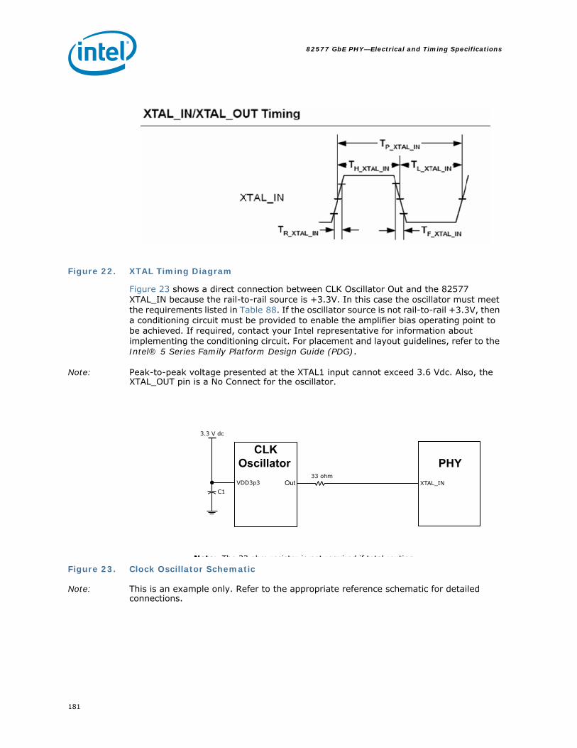
82577 GbE PHY—Electrical and Timing Specifications
181
Figure 22. XTAL Timing Diagram
Figure 23 shows a direct connection between CLK Oscillator Out and the 82577 XTAL_IN because the rail-to-rail source is +3.3V. In this case the oscillator must meet the requirements listed in Table 88. If the oscillator source is not rail-to-rail +3.3V, then a conditioning circuit must be provided to enable the amplifier bias operating point to be achieved. If required, contact your Intel representative for information about implementing the conditioning circuit. For placement and layout guidelines, refer to the Intel® 5 Series Family Platform Design Guide (PDG).
Note: Peak-to-peak voltage presented at the XTAL1 input cannot exceed 3.6 Vdc. Also, the XTAL_OUT pin is a No Connect for the oscillator.
Figure 23. Clock Oscillator Schematic
Note: This is an example only. Refer to the appropriate reference schematic for detailed connections.

182
Electrical and Timing Specifications—82577 GbE PHY
Note: This page intentionally left blank.

82577 GbE PHY—Schematic and Board Layout Checklists
183
12.0 Schematic and Board Layout Checklists
The 82577 schematic and board layout checklists can be found at www.intel.com.

184
Schematic and Board Layout Checklists—82577 GbE PHY
Note: This page intentionally left blank.

82577 GbE PHY—Reference Schematics
185
13.0 Reference Schematics
The 82577 reference schematics can be found at www.intel.com.

186
Reference Schematics—82577 GbE PHY
Note: This page intentionally left blank.

82577 GbE PHY—Models
187
14.0 Models
Contact your local Intel representative for access.

188
Models—82577 GbE PHY
Note: This page intentionally left blank.