integrated circuit diagnostic tools: underlying physics ... bound... · integrated circuit...
TRANSCRIPT
Philips Journalof Research Vol.44 Nos 2/3 1989 295
Philips J. .Res. 44, 295-327, 1989 R 1212
INTEGRATED CIRCUIT DIAGNOSTIC TOOLS:UNDERLYING PHYSICS AND
APPLICATIONS
by C.G.C. DE KORT
Philips Research Laboratories. P.O. Box 80000. 5600 JA. Eindhoven. TIle Netherlands
Abstract
In this article methods and tools are discussed which yield information onthe electrical performance of integrated circuits (ICs) by means other thanelectrical testing via input and output pins. We consider methods formaking measurements inside ICs, revealing fault locations and determiningthe time dependence of internal voltages. Secondly, measurements forlocating weak spots within the IC are considered. It is shown that repaircan play a vital role in improving the efficiency of testing.A set-up for performing repairs is discussed. The working principlesunderlying the dilTerent methods and tools are explained and examples aregiven to illustrate their usefulness. Finally, the impact of new technologieson the development of diagnostic methods and tools is discussed.
Keywords: alpha particles, diagnostic tools, electron beam, electro-optic,integrated circuits, latch-up, light emission, liquid crystal,secondary electrons, testing, waveform
1. Introduetion
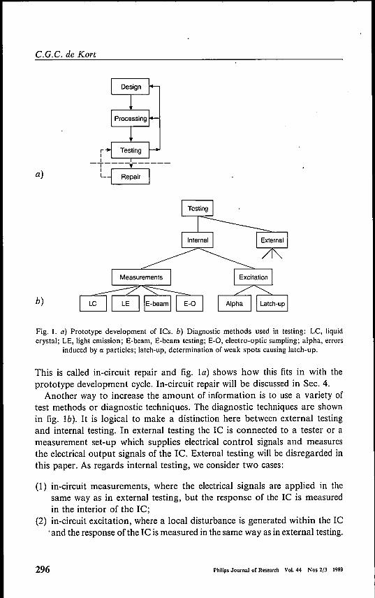
The prototype development of an integrated circuit (IC) comprises thedesign, processing and testing of an IC such as that shown schematically infig. la). Prototype development time should be kept as short as possible. Thisimplies that the time needed for each step shown in fig. la) should be carefullyconsidered so that it can be further reduced. Prototype development normallyrequires several loops (redesigns) before an error-free and optimaIiyfunctioning device is obtained, complying with the process technology. Tominimize the number of redesigns it is important to gain a maximum amountof information about the ICs processed. One way to increase the amount ofinformation is to make it possible to repair fatal errors within the chip.
296 Philips Journalof Research Vol.44 Nos 2/3 1989
C.G.C. de Kort
a)
rII-T----.------l_~ Repair
b)
Fig. 1. a) Prototype development of lCs. b) Diagnostic methods used in testing: LC, liquidcrystal; LE, light emission; E-beam, E-beam testing; E-O, electro-optic sampling; alpha, errors
induced by exparticles; latch-up, determination of weak spots causing latch-up.
This is called in-circuit repair and fig. la) shows how this fits in with theprototype development cycle. In-circuit repair will be discussed in Sec. 4.
Another way to increase the amount of information is to use a variety oftest methods or diagnostic techniques. The diagnostic techniques are shownin fig. 1b). It is logical to make a distinction here between external testingand internal testing. In external testing the IC is connected to a tester or ameasurement set-up which supplies electrical control signals and measuresthe electrical output signals of the IC. External testing will be disregarded inthis paper. As regards internal testing, we consider two cases:
(1) in-circuit measurements, where the electrical signals are applied in thesame way as in external testing, but the response of the IC is measuredin the interior of the IC;
(2) in-circuit excitation, where a local disturbance is generated within the IC.and the response ofthe IC ismeasured in the same way as in external testing.
I C diagnostic tools
In-circuit measurements will be dealt with in Sec. 2 and in-circuit excitationwill be discussed in Sec. 3. The goal of in-circuit measurements is either todetermine a fault location or to verify the performance of the circuit at aninternal node. In-circuit excitation provides information about theperformance of the IC under unusual conditions and can reveal the locationof weak spots within the IC.
The various ways to perform internal testing require different diagnostictools which rely on a number of physical phenomena. This paper explains thebasic physical principles which underlie the diagnostic tools and the use ofeach is illustrated by an example. In Secs 2-4 the methods and tools currentlyin use and/or under development in this laboratory are discussed. Section 5presents a comparison with other in-circuit measurement tools and deals withthe impact of new IC technologies on the usefulness of the different tools.
2. In-circuit measurements
In-circuit measurements are concerned with the physical parameters withinthe IC whose value is influenced by the local functioning of the IC. Examplesare temperature and electric field. The values of these physical parameterscontain information about the local functioning of the IC. The type ofinformation depends on the parameter which is being measured. In this sectionwe will describe several in-circuit measurement tools and methods, besidesexplaining how the physical parameter related to each tool is measured. Theoperating conditions and limitations are considered next. Finally, theapplication field is indicated and each method is illustrated by an example.
2.1. Liquid crystal techniques
Failures in ICs often lead to an increase in current, which causes a smallrise in temperature. Liquid crystals (LCs) are used to visualize the temperaturedistribution within the IC 1-7). Nemati~ LCs with a first-order phase transitionat the clearing point 7;, are most appropriate for this purpose. Below 7;, theLC material is in the nematic (ordered) state, showing optical anisotropy,while above T., it is isotropic. This difference in optical properties is used todetermine whether or not the local temperature is above 7;,.
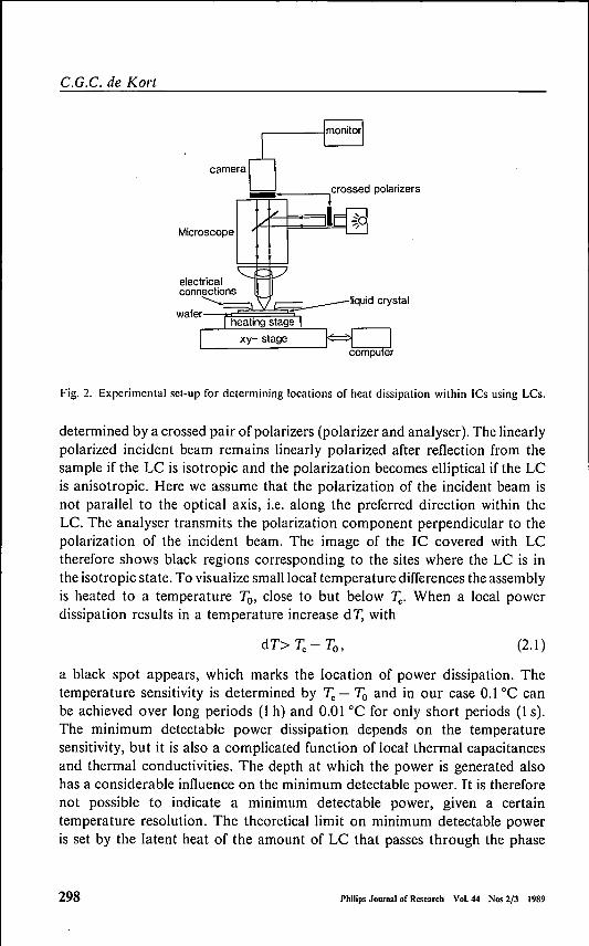
In the experimental set-up, shown schematically in fig. 2, a microscope isused to examine the IC. It is fixed on a heating stage in the form of a waferor a mounted device. The whole assembly can be moved by acomputer-controlled x-y stage. Electrical connections are provided to drivethe IC. In the microscope the state of the LC materialon top of the IC is
Philips Journalof Research Vol.44 Nos 2/3 1989 297
(2.1 )
C.G.C. de Kort
Fig. 2. Experimental set-up for determining locations of heat dissipation within ICs using LCs.
determined by a crossed pair of polarizers (polarizer and analyser). The linearlypolarized incident beam remains linearly polarized after reflection from thesample if the LC is isotropic and the polarization becomes elliptical if the LCis anisotropic. Here we assume that the polarization of the incident beam isnot parallel to the optical axis, i.e. along the preferred direction within theLC. The analyser transmits the polarization component perpendicular to thepolarization of the incident beam. The image of the IC covered with LCtherefore shows black regions corresponding to the sites where the LC is inthe isotropic state. To visualize smalllocal temperature differences the assemblyis heated to a temperature To, close to but below 7;,. When a local powerdissipation results in a temperature increase dT, with
a black spot appears, which marks the location of power dissipation. Thetemperature sensitivity is determined by 7;, - To and in our case 0.1 °C canbe achieved over long periods (1 h) and 0.01 °C for only short periods (1 s).The minimum detectable power dissipation depends on the temperaturesensitivity, but it is also a complicated function of local thermal capacitancesand thermal conductivities. The depth at which the power is generated alsohas a considerable influence on the minimum detectable power. It is thereforenot possible to indicate a minimum detectable power, given a certaintemperature resolution. The theoretical limit on minimum detectable poweris set by the latent heat of the amount of Le that passes through the phase
298 Philips Journalof Research Vol. 44 Nos 2/3 1989
I C diagnostic tools
transition from nematic to isotropic. The spatial resolution is determined bythe optics of the microscope and in our set-up is 1 urn. The minimum energyrequired as latent heat for the phase transition of a l um spot and a layerthickness of 2 urn is found to be between 1 . 10- 11 and 2· 10 - 11 J. For an orderof magnitude estimate we take a thermal time constant of 0.1 s for the Ie-LCassembly. Then the minimum power required for the phase transition to occuris between 1.10-10 and 2·10-1oW, which is much lower than the powerrequired to give a dT corresponding to eq. (2.1) in all practical cases.
The LC generally used is ROCE 1510 from Hoffmann LaRoche 6), whichhas a ~ of 48.0 °C. At room temperature this material is in the solid phaseand it melts at 44.5 °C. A few drops of a saturated acetone solution are appliedto a wafer or a packaged IC 4). The acetone evaporates in about 1min, leavingbehind a thin layer of solid LC material. The procedure described above isthen followed to reveal the locations of power dissipation. By moving andpositioning the wafer with respect to the probe-card, each IC (or die) presenton a wafer can be examined.
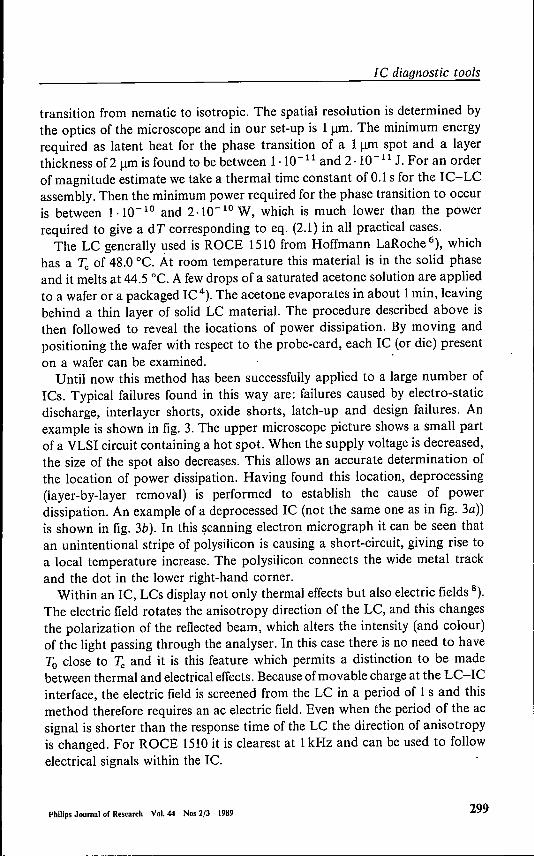
Until now this method has been successfully applied to a large number ofICs. Typical failures found in this way are: failures caused by electro-staticdischarge, interlayer shorts, oxide shorts, latch-up and design failures. Anexample is shown in fig. 3. The upper microscope picture shows a small partof a VLSI circuit containing a hot spot. When the supply voltage is decreased,the size of the spot also decreases. This allows an accurate determination ofthe location of power dissipation. Having found this location, deprocessing(layer-by-layer removal) is performed to establish the cause of powerdissipation. An example of a deprocessed IC (not the same one as in fig. 3a))is shown in fig. 3b). In this scanning electron micrograph it can be seen thatan unintentional stripe of polysilicon is causing a short-circuit, giving rise toa local temperature increase. The polysilicon connects the wide metal trackand the dot in the lower right-hand corner.
Within an IC, LCs display not only thermal effects but also electric fields 8).The electric field rotates the anisotropy direction of the LC, and this changesthe polarization of the reflected beam, which alters the intensity (and colour)of the light passing through the analyser. In this case there is no need to haveTo close to ~ and it is this feature which permits a distinction to be madebetween thermal and electrical effects. Because ofmovable charge at the Le-ICinterface, the electric field is screened from the Le in a period of 1 s and thismethod therefore requires an ac electric field. Even when the period of the acsignal is shorter than the response time of the LC the direction of anisotropyis changed. For ROCE 1510 it is clearest at 1 kHz and can be used to followelectrical signals within the IC.
Philips Journni of Research Vol.44 Nos 2/3 1989 299
CC.C. de Kort
a)
b)
Fig. 3. Application of the LC method: a) a microscope picture of an IC containing a hot spot;b) a deprocessed IC showing the cause of heat dissipation.
2.2. Light emission
Light emission from chips has been known for a long time. Until recently,however, it was oflimited value as a diagnostic tool. This situation has changeddramatically with the introduetion of high gain image intensifiers, which allow
300 Philips .Journal of Research Vol.44 Nos 213 1989
IC diagnostic tools
electron path fluorescent screen
fibre opticwindow photocathode
microchannel plate
fibre opticwindow
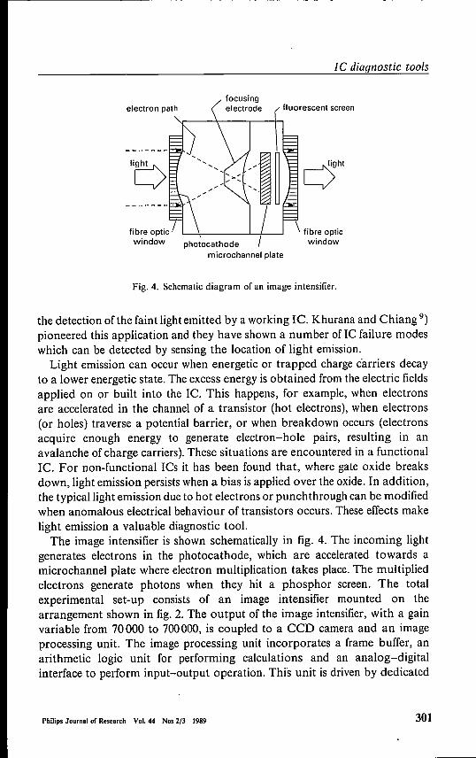
Fig. 4. Schematic diagram of an image intensilier.
the detection ofthe faint light emitted by a working IC. Khurana and Chiang 9)pioneered this application and they have shown a number oflC failure modeswhich can be detected by sensing the location of light emission.
Light emission can occur when energetic or trapped charge carriers decayto a lower energetic state. The excess energy is obtained from the electric fieldsapplied on or built into the IC. This happens, for example, when electronsare accelerated in the channel of a transistor (hot electrons), when electrons(or holes) traverse a potential barrier, or when breakdown occurs (electronsacquire enough energy to generate electron-hole pairs, resulting in anavalanche of charge carriers). These situations are encountered in a functionalIC. For non-functional ICs it has been found that, where gate oxide breaksdown, light emission persists when a bias is applied over the oxide. In addition,the typicallight emission due to hot electrons or punchthrough can be modifiedwhen anomalous electrical behaviour of transistors occurs. These effects makelight emission a valuable diagnostic tool.
The image intensifier is shown schematically in fig. 4. The incoming lightgenerates electrons in the photocathode, which are accelerated towards amicrochannel plate where electron multiplication takes place. The multipliedelectrons generate photons when they hit a phosphor screen. The totalexperimental set-up consists of an image intensifier mounted on thearrangement shown in fig. 2. The output of the image intensifier, with a gainvariable from 70000 to 700000, is coupled to a CCD camera and an imageprocessing unit. The image processing unit incorporates a frame buffer, anarithmetic logic unit for performing calculations and an analog-digitalinterface to perform input-output operation. This unit is driven by dedicated
Philips Journalof Research Vol. 44 Nos 2/3 1989 301
C.C.C. de Kort
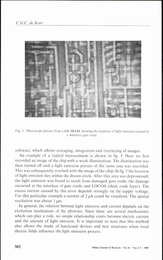
Fig. 5. Microscope picture from a 64k SRAM showing the location of light emission caused bya defective gate oxide.
software, which allows averaging, integration and overlaying of images.An example of a typical measurement is shown in fig. 5. Here we first
recorded an image of the chip with a weak illumination. The illumination wasthen turned off and a light emission picture of the same area was recorded.This was subsequently overlaid with the image ofthe chip. In fig. 5 the locationof light emission lies within the drawn circle. After this area was deprocessed,the light emission was found to result from damaged gate oxide; the damageoccurred at the interface of gate oxide and LOCOS (thick oxide layer). Theexcess current caused by this error depends strongly on the supply voltage.For this particular example a current of 2 flÄ could be visualized. The spatialresolution was about I 1J.I11.
In general, the relation between light emission and current depends on theexcitation mechanism of the photons. Since there are several mechanismswhich can play a role, no simple relationship exists between electric currentand the amount of light emission. It is important to note that this methodalso allows the study of functional devices and test structures when localelectric fields influence the light emission process.
302 Philips Journalof Research Vol. 44 Nos 2/3 1989
IC diagnostic tools
2.3. Electron beam techniques
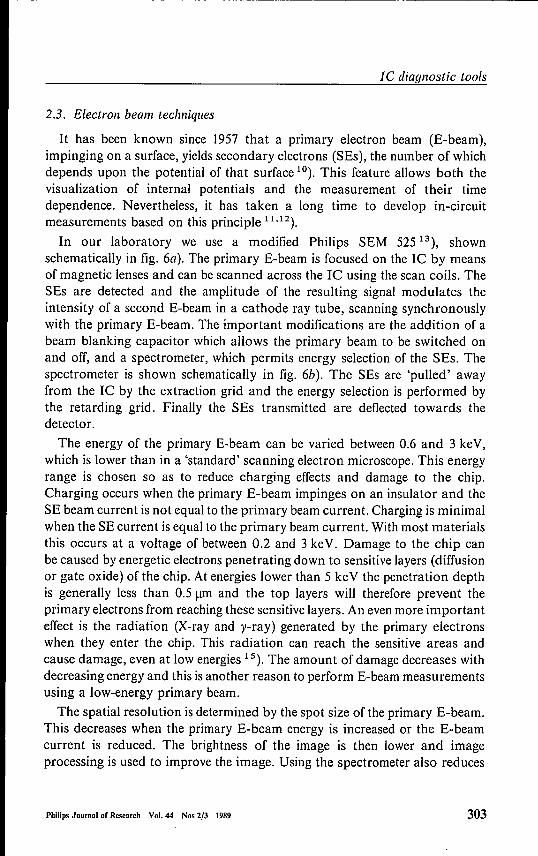
It has been known since 1957 that a primary electron beam (E-beam),impinging on a surface, yields secondary electrons (SEs), the number of whichdepends upon the potentialof that surface 10). This feature allows both thevisualization of internal potentials and the measurement of their timedependence. Nevertheless, it has taken a long time to develop in-circuitmeasurements based on this principle 11.12).
In our laboratory we use a modified Philips SEM 52513), shownschematically in fig. 6a). The primary E-beam is focused on the IC by meansof magnetic lenses and can be scanned across the IC using the scan coils. TheSEs are detected and the amplitude of the resulting signal modulates theintensity of a second E-beam in a cathode ray tube, scanning synchronouslywith the primary E-beam. The important modifications are the addition of abeam blanking capacitor which allows the primary beam to be switched onand off, and a spectrometer, which permits energy selection of the SEs. Thespectrometer is shown schematically in fig. 6b). The SEs are 'pulled' awayfrom the IC by the extraction grid and the energy selection is performed bythe retarding grid. Finally the SEs transmitted are deflected towards thedetector.
The energy of the primary E-beam can be varied between 0.6 and 3 keY,which is lower than in a 'standard' scanning electron microscope. This energyrange is chosen so as to reduce charging effects and damage to the chip.Charging occurs when the primary E-beam impinges on an insulator and theSE beam current is not equal to the primary beam current. Charging is minimalwhen the SE current is equal to the primary beam current. With most materialsthis occurs at a voltage of between 0.2 and 3 keY. Damage to the chip canbe caused by energetic electrons penetrating down to sensitive layers (diffusionor gate oxide) of the chip. At energies lower than 5 keV the penetration depthis generally less than 0.5 J.Ul1 and the top layers will therefore prevent theprimary electrons from reaching these sensitive layers. An even more importanteffect is the radiation (X-ray and y-ray) generated by the primary electronswhen they enter the chip. This radiation can reach the sensitive areas andcause damage, even at low energies 15). The amount of damage decreases withdecreasing energy and this is another reason to perform E-beam measurementsusing a low-energy primary beam.
The spatial resolution is determined by the spot size of the primary E-beam.This decreases when the primary E-beam energy is increased or the E-beamcurrent is reduced. The brightness of the image is then lower and imageprocessing is used to improve the image. Using the spectrometer also reduces
Philips Journalof Research Vol.44 Nos 2/3 1989 303
wc.;..
~,[...oc:;e,sa,
'"~;::...-e~tz51~:ëag
PE-beam 5V+ /
~.IJEt;;ETrnp ,......,J
V,-120Vi~,;oo -;':.5V10~V) 6~V 40V 20V 10Vd~ v,-ov-----+-~---1-- :f~""i"<"'id ~
! ê1------ 400V -
Blanking capacitor
Primary electron beam
ic-package
a)x-y stage t----i
1mmb) Retarding field spectrometer
Fig.6. a) E-beam column and vacuum chamber used to perform E-beam testing. b) Spectrometer used to obtain an energy selection of the secondaryelectrons. This figure is taken from ref. 14.
(")ë;)o~!1>
7>:c........
IC diaqnostic tools
the brightness of the image, because it cuts down the number of SEs capableof reaching the detector. Time resolution will be discussed below, togetherwith waveform measurements. The E-beam tester can be operated in severalmodes which are selected according to the application envisaged. Some ofthese modes will be discussed in the following sections.
2.3.1. Static voltage contrast
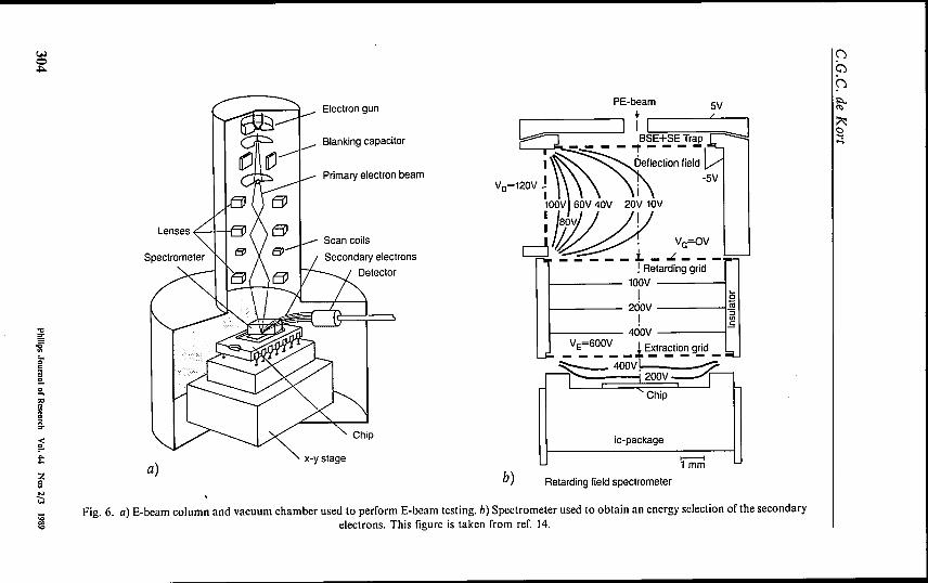
In the static voltage contrast mode a picture of part of the IC is displayedas described above. The spectrometer can enhance the voltage contrast. Withproper settings the electrons coming from lines at 0 V are transmitted, whilemost ofthe electrons departing from lines at + 5 V are reflected. This measuringmode is suitable for displaying static (or low frequency) voltages within the IC.
An example of it is given in fig. 7, with part of a 64k SRAM. Here thebright lines are at 0 V and the dark lines at 5 V. By observing the staticvoltages for different input signals it was found that the y-write signals, in theupper part of fig. 7a), were connected with the bit lines in the lower part.After deprocessing this area it was found that an aluminium track passing acontact hole was short circuited to this contact hole by an aluminiumfilament 16), as shown in fig. 7b).
2.3.2. Stroboscopic voltage contrast
In the stroboscopic voltage contrast mode the signal frequency applied tothe chip is a multiple of the scan frequency of the E-beam. Thus each timethe E-beam crosses a given location it probes the same phase of the electricsignal, resulting in a static picture. During scanning, different points on thesame line are at a different phase, which gives rise to black and white blocksin the case of digital signals. This measuring mode is used to display and trackac signals within the IC.
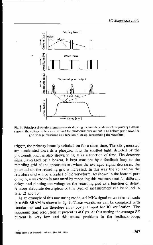
2.3.3. Waveform measurement
In order to measure the time dependence of internal IC signals, the primarybeam is fixed at a circuit node which carries the signal. To achieve a hightime resolution the primary beam is pulsed by a short electrical pulse drivingthe beam blanker. This is necessary when the SE detector response time limitsthe time resolution and then the duration of the beam blanking pulsedetermines the time resolution. The beam blanking pulse is synchronized withthe signal frequency, as shown in fig. 8. The top curve illustrates the timedependence of the primary E-beam current. After a delay, measured from
Philips Journalof Research Vol.44 Nos 2/3 1989 305
306 Philips Joumal of Research Vol. 44 Nos 2/J 1989
c.c.c. de Kort
al
b)
Fig. 7. a) Voltage contrast picture made with the E-beam tester on a 64k SRAM showing linesat zero potential (white) on y-write lines (upper part) and bit lines (lower part). b) Aluminium
filament causing a short circuit between bit lines and y-write lines.
IC diaqnostic tools
Primary beam
!j dQti'~ ~L____
Wave form
t~0.E«
Photomultiplier output
- Delay la.u.l
Fig. 8. Principle of waveform measurements showing the time dependence of the primary E-beamcurrent, the voltage to be measured and the photomultiplier output. The bottom part shows the
grid voltage measured as a function of delay, representing the waveform.
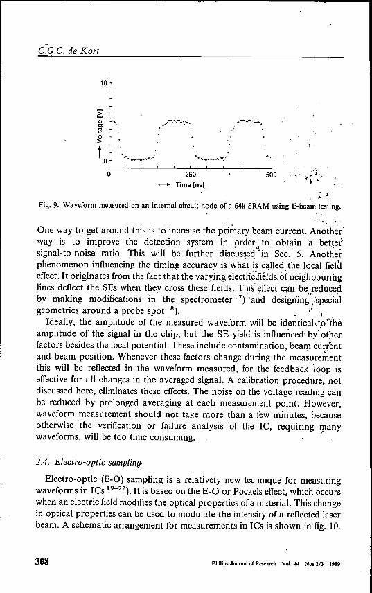
trigger, the primary beam is switched on for a short time. The SEs generatedare accelerated towards a phosphor and the emitted light, detected by thephotomultiplier, is also shown in fig. 8 as a function of time. The detectorsignal, averaged by a boxcar, is kept constant by a feedback loop to theretarding grid of the spectrometer: when the averaged signal decreases, thepotential on the retarding grid is increased. In this way the voltage on theretarding grid will be a replica of the waveform. As shown in the bottom partof fig. 8, a waveform is measured by repeating this measurement for differentdelays and plotting the voltage on the retarding grid as a function of delay.A more elaborate description of this type of measurement can be found inrefs. 12 and 13.As an example of this measuring mode, a 4 MHz signalon an internal node
in a 64k SRAM is shown in fig. 9. These waveforms can be compared withsimulations and are therefore an important input for IC verification. Theminimum time resolution at present is 400 ps. At this setting the average SEcurrent is very low and this causes problems in the feedback loop.
Philips Journalof Research Vol.44 Nos 2/3 1989 307
... ..'
C.G.C. de Kort
10
". ....:..:-,-...:... ...............
._._...." .._ ....,..: ....._ ...._ ..--; .. .....
o 250.,...-+ Time lnsl
500
Fig. 9. Waveform measured on an internal circuit node of a 64k SRAM using E-beam testing.,......
One way to get around this is to increase the primary beam current. Anotherway is to improve the detection system in order to obtain a bët.~èr:
. "t , ..
signal-to-noise ratio. This will be further discussed" in Sec. 5. Anotherphenomenon influencing the timing accuracy is what i~ called the local .fieldeffect. It originates from the fact that the varying electfié~fiélds,ófneighbourihglines deflect the SEs when they cross these fields. This' effect can-be reducedby making modifications in the spectrometer 17) 'and designingjspècialgeometries around a probe spot 18). ~ i'l I j:
Ideally, the amplitude of the measured waveform will be identical.to'théamplitude of the signal in the chip, but the SE yield is influenced byotherfactors besides the local potential. These include contamination, beam currentand beam position, Whenever these factors change during the measurementthis will be reflected in the waveform measured, for the feedback loop iseffective for all changes in the averaged signal. A calibration procedure, notdiscussed here, eliminates these effects. The noise on the voltage reading canbe reduced by prolonged averaging at each measurement point. However,waveform measurement should not take more than a few minutes, becauseotherwise the verification or failure analysis of the rc, requiring lJlanywaveforms, will be too time consuming.
2.4. Electro-optic sampling.
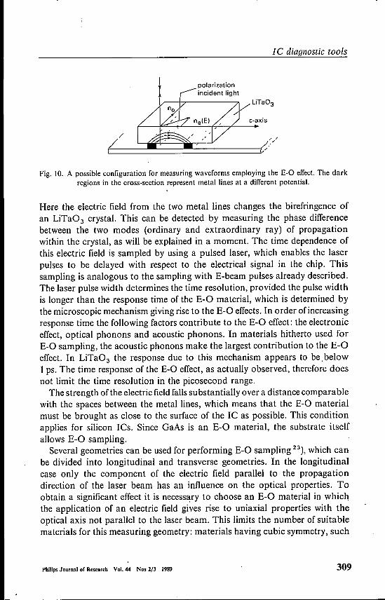
Electro-optic (E-O) sampling is a relatively new technique for measuringwaveforms in LCs 19-22). It is based on the E-O or Pockels effect, which occurswhen an electric field modifies the optical properties of a material. This changein optical properties can be used to modulate the intensity of a reflected laserbeam. A schematic arrangement for measurements in LCs is shown in fig. 10.
308 Philips Journalof Research Vol.44 Nos 2/3 1989
IC diaqnostic tools
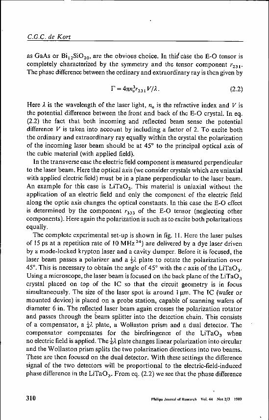
polarizationincident light
/
é:/==~==~=======t./.Fig. 10. A possible configuration for measuring waveforms employing the E-O effect. The dark
regions in the cross-section represent metal lines at a different potential.
Here the electric field from the two metal lines changes the birefringence ofan LiTa03 crystal. This can be detected by measuring the phase differencebetween the two modes (ordinary and extraordinary ray) of propagationwithin the crystal, as will be explained in a moment. The time dependence ofthis electric field is sampled by using a pulsed laser, which enables the laserpulses to be delayed with respect to the electrical signal in the chip. Thissampling is analogous to the sampling with E-beam pulses already described.The laser pulse width determines the time resolution, provided the pulse widthis longer than the response time of the E-O material, which is determined bythe microscopie mechanism giving rise to the E-O effects. In order of increasingresponse time the following factors contribute to the E-O effect: the electroniceffect, optical phonons and acoustic phonons. In materials hitherto used forE-O sampling, the acoustic phonons make the largest contribution to the E-Oeffect. In LiTa03 the response due to this mechanism appears to be below1ps. The time response of the E-O effect, as actually observed, therefore doesnot limit the time resolution in the picosecond range.The strength of the electric fieldfallssubstantially over a distance comparable
with the spaces between the metal lines, which means that the E-O materialmust be brought as close to the surface of the IC as possible. This conditionapplies for silicon ICs. Since GaAs is an E-O material, the substrate itselfallows E-O sampling.Several geometries can be used for performing E-O sampling 23), which can
be divided into longitudinal and transverse geometries. In the longitudinalcase only the component of the electric field parallel to the propagationdirection of the laser beam has an influence on the optical properties. Toobtain a significant effect it is necessary to choose an E-O material in whichthe application of an electric field gives rise to uniaxial properties with theoptical axis not parallel to the laser beam. This limits the number of suitablematerials for this measuring geometry: materials having cubic symmetry, such
Philips Journalof Research Vol. 44 Nos 2/3 1989 309
(2.2)
C.G.C. de Kort
as GaAs or Bi12Si020, are the obvious choice. In this' case the E-O tensor iscompletely characterized by the symmetry and the tensor component r231.The phase difference between the ordinary and extraordinary ray is then given by
Here Ä is the wavelength of the laser light, no is the refractive index and V isthe potential difference between the front and back of the E-O crystal. In eq.(2.2) the fact that both incoming and reflected beam sense the potentialdifference V is taken into account by including a factor of 2. To excite boththe ordinary and extraordinary ray equally within the crystal the polarizationof the incoming laser beam should be at 45° to the principal optical axis ofthe cubic material (with applied field).In the transverse case the electric fieldcomponent is measured perpendicular
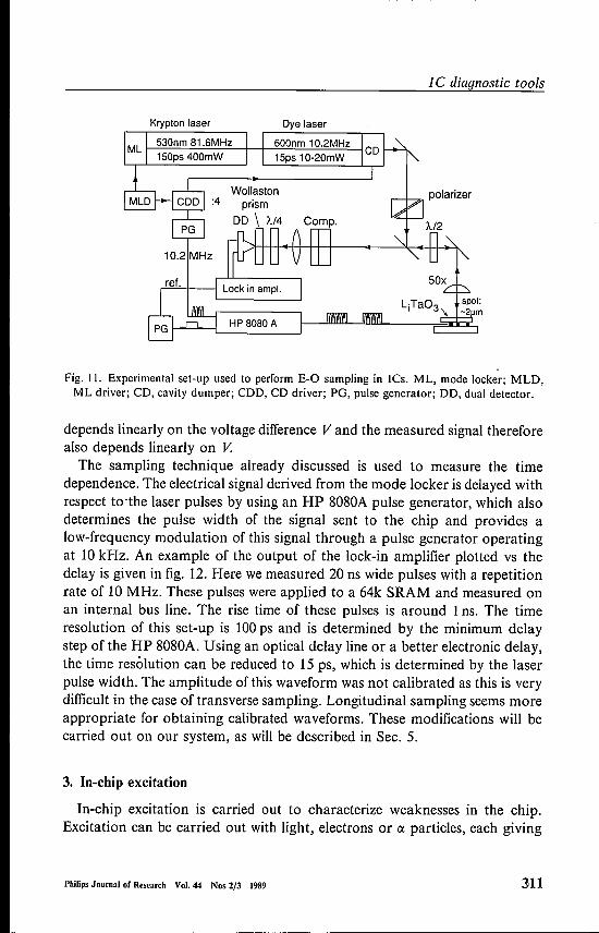
to the laser beam. Here the optical axis (we consider crystals which are uniaxialwith applied electric field) must be in a plane perpendicular to the laser beam.An example for this case is LiTa03• This material is uniaxial without theapplication of an electric field and only the component of the electric fieldalong the optic axis changes the optical constants. In this case the E-O effectis determined by the component r333 of the E-O tensor (neglecting othercomponents). Here again the polarization is such as to excite both polarizationsequally.The complete experimental set-up is shown in fig. 11. Here the laser pulses
of 15 ps at a repetition rate of 10 MHz 24) are delivered by a dye laser drivenby a mode-locked krypton laser and a cavity dumper. Before it is focused, thelaser beam passes a polarizer and a tÄ plate to rotate the polarization over45°. This is necessary to obtain the angle of 45° with the c axis of the LiTa03•Using a microscope, the laser beam is focused on the back plane ofthe LiTa03crystal placed on top of the IC so that the circuit geometry is in focussimultaneously. The size of the laser spot is around 1urn. The IC (wafer ormounted device) is placed on a probe station, capable of scanning wafers ofdiameter 6 in. The reflected laser beam again crosses the polarization rotatorand passes through the beam splitter into the detection chain. This consistsof a compensator, a iÄ plate, a Wollaston prism and a dual detector. Thecompensator compensates for the birefringence of the LiTa03 whenno electric field is applied. The iÄ plate changes linear polarization into circularand the Wollaston prism splits the two polarization directions into two beams:These are then focused on the dual detector. With these settings the differencesignalof the two detectors will be proportional to the electric-field-inducedphase difference in the LiTa03. From eq. (2.2) we see that the phase difference
310 Philips Journalof Research Vol.44 Nos 2/3 1989
I C diagnostic tools
Krypton laser Dyelaser
150ps 400mW600nm 10.2MHz530nm 81.6MHz
15ps 10-20mW
Wollaston
Fig. 11. Experimental set-up used to perform E-O sampling in ICs. ML, mode locker; MLD,ML driver; CD, cavity dumper; CDD, CD driver; PG, pulse generator; DD, dual detector.
depends linearlyon the voltage difference V and the measured signal thereforealso depends linearlyon V.
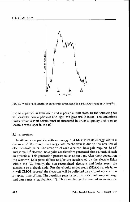
The sampling technique already discussed is used to measure the timedependence. The electrical signal derived from the mode locker is delayed withrespect to-the laser pulses by using an HP 8080A pulse generator, which alsodetermines the pulse width of the signal sent to the chip and provides alow-frequency modulation of this signal through a pulse generator operatingat 10 kHz. An example of the output of the lock-in amplifier plotted vs thedelay is given in fig. 12. Here we measured 20 ns wide pulses with a repetitionrate of 10 MHz. These pulses were applied to a 64k SRAM and measured onan internal bus line. The rise time of these pulses is around 1ns. The timeresolution of this set-up is 100 ps and is determined by the minimum delaystep of the HP 8080A. Using an optical delay line or a better electronic delay,the time resolution can be reduced to 15 ps, which is determined by the laserpulse width. The amplitude of this waveform was not calibrated as this is verydifficult in the case of transverse sampling. Longitudinal sampling seems moreappropriate for obtaining calibrated waveforms. These modifications will becarried out on our system, as will be described in Sec. 5.
3. In-chip excitation
In-chip excitation is carried out to characterize weaknesses in the chip.Excitation can be carried out with light, electrons or a particles, each giving
Philips Journalof Research Vol.44 Nos 2/3 1989 311
C.G.C. de Kort
t
40 50 60-- Delay[ns)
Fig. 12. Waveform measured on an internal circuit node of a 64k SRAM using E-O sampling.
rise to a particular behaviour and a possible fault state. In the following wewill describe how IX particles and light can give rise to faults. The conditionsunder which a fault occurs must be measured in order to qualify a chip or tolocate a weak spot in the IC.
3.1. IX particles
In silicon an IX particle with an energy of 4 MeV loses its energy within adistance of 30 J..UD and the energy loss mechanism is due to the creation ofelectron-hole pairs. The creation of each electron-hole pair requires 3.6 eVand some 106 electron-hole pairs are therefore generated along a path of such'an IX particle. This generation process takes about 1ps. After their generationthe electron-hole pairs diffuse and/or are accelerated by the electric fieldswithin the IC. Finally, the non-recombined electrons and holes reach thesubstrate or a circuit node. For the circuits under study (SRAMs made in ann-well CMOS process) the electrons will be collected on a circuit node withina typical time of 1ns. The resulting peak current is in the milliampère rangeand can cause a malfunction 25). This can change the content in memories.
312 Philip. Journal of Research Vol.44 Nos 2/3 1989
IC diagnostic tools
When the affected memory cell is rewritten this error disappears. Thesea-induced errors are therefore referred to as soft errors and the rate at whichthey occur is referred to as the soft error rate (SER).
a Particles emitted by natural abundance radioactive impurities have anenergy of between 2 and 9 MeV and the number of a particles reaching anIC is determined by the radioactive impurity content of the materialssurrounding the IC. A layer of only some 30 urn facing the chip will contribute.The materials used in the chip production also contribute in so far as theycontain radioactive isotopes. For moulding plastic HC 10-2 TX 003509 it wasfound that an a particle is entering a chip of 1crrr' once in every 100h 26.27).
Assuming that one out of every thousand a particles creates an error, thismeans that an error occurs once in every 105h. Though this error rate mayseem low, it still creates a serious threat to the reliability of memory devices.The requirements as to reliability are expressed in FITs (1 FIT is defined asone failure in 109 device hours). For the SER the requirement is generallybelow 1000 FIT and the example given above would exceed this by a factorof 10. However improbable the arrival of an a particle may seem, therefore,the a particle sensitivity of present-day memory devices has to be known.To determine the SER the measurements are accelerated by exposing the
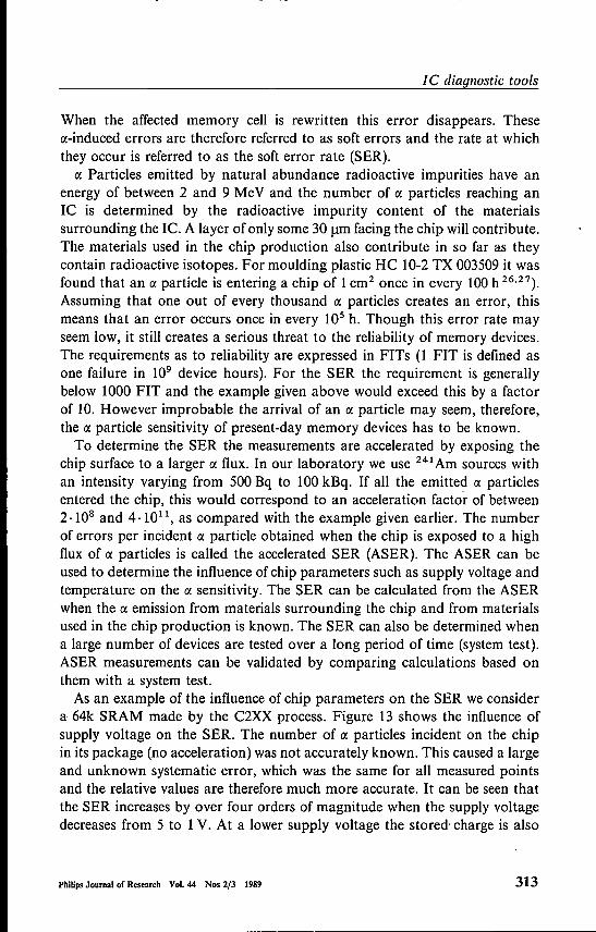
chip surface to a larger a flux. In our laboratory we use 241Am sources withan intensity varying from 500 Bq to 100 kBq. If all the emitted a particlesentered the chip, this would correspond to an acceleration factor of between2.108 and 4.1011, as compared with the example given earlier. The numberof errors per incident a particle obtained when the chip is exposed to a highflux of a particles is called the accelerated SER (ASER). The ASER can beused to determine the influence of chip parameters such as supply voltage andtemperature on the a sensitivity. The SER can be calculated from the ASERwhen the a emission from materials surrounding the chip and from materialsused in the chip production is known. The SER can also be determined whena large number of devices are tested over a long period of time (system test).ASER measurements can be validated by comparing calculations based onthem with a system test.As an example of the influence of chip parameters on the SER we consider
a 64k SRAM made by the C2XX process. Figure 13 shows the influence ofsupply voltage on the SER. The number of a particles incident on the chipin its package (no acceleration) was not accurately known. This caused a largeand unknown systematic error, which was the same for all measured pointsand the relative values are therefore much more accurate. It can be seen thatthe SER increases by over four orders of magnitude when the supply voltagedecreases from 5 to 1V. At a lower supply voltage the stored' charge is also
Philips Journalof Research Vol.44 Nos 2/3 1989 313
314 Philip. Journalof Research Vol.44 Nos 2/3 1989
C.G.C. de Kort
Î
--0--- Pattern B
---0--- Pattern A
SER (FITS)
'0"''1\
'1>......
'6.........'6 ............
"6 ....
-,"'0
............... ...,
"'0
10 L-----'_----'- _ __.__J...._----'_----'-_--'------'
1.0 2.0 3.0 4.0 5.0- Supply voltage (V)
Fig. 13. Soft error rate induced by IX particles as a function of supply voltage for a 64k SRAM.Measurements were done for two dilTerent patterns (A and B) resident in the memory.
lower, which makes it easier for the 'fixed amount' of injected charge to causean error. These measurements were done for two different patterns writteninto the SRAM. Both the dependence on supply voltage and the dependenceon pattern agree with circuit simulations 27). The strong dependence on supplyvoltage is important when one is considering memories with low-voltagebattery back-up or future generations of memories operating at lower supplyvoltages.
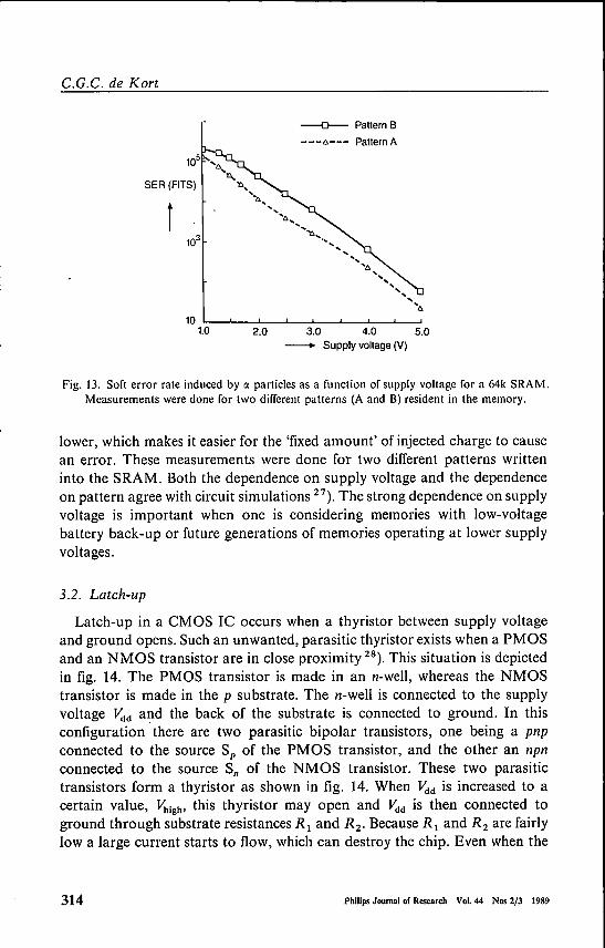
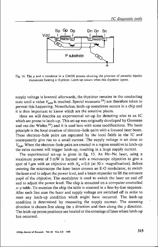
3.2. Latch-up
Latch-up in a CMOS IC occurs when a thyristor between supply voltageand ground opens. Such an unwanted, parasitic thyristor exists when a PMOSand an NMOS transistor are in close proximity 28). This situation is depictedin fig. 14. The PMOS transistor is made in an n-well, whereas the NMOStransistor is made in the p substrate. The n-well is connected to the supplyvoltage Vdd and the back of the substrate is connected to ground. In thisconfiguration there are two parasitic bipolar transistors, one being a pnpconnected to the source S, of the PMOS transistor, and the other an npnconnected to the source Sn of the NMOS transistor. These two parasitictransistors form a thyristor as shown in fig. 14. When Vdd is increased to acertain value, Vhigh, this thyristor may open and Vdd is then connected toground through substrate resistances RI and R2• Because RI and R2 are fairlyIowa large current starts to flow, which can destroy the chip. Even when the
IC diaqnostic tools
Fig. 14. The pand 11 transistor in a CMOS process showing the presence of parasitic bipolartransistors forming a thyristor. Latch-up occurs when this thyristor opens.
supply voltage is lowered afterwards, the thyristor remains in the conductingstate until a value Vhold is reached. Special measures 29) are therefore taken toprevent this happening. Nonetheless, latch-up sometimes occurs in a chip andit is then important to know which are the sensitive places.
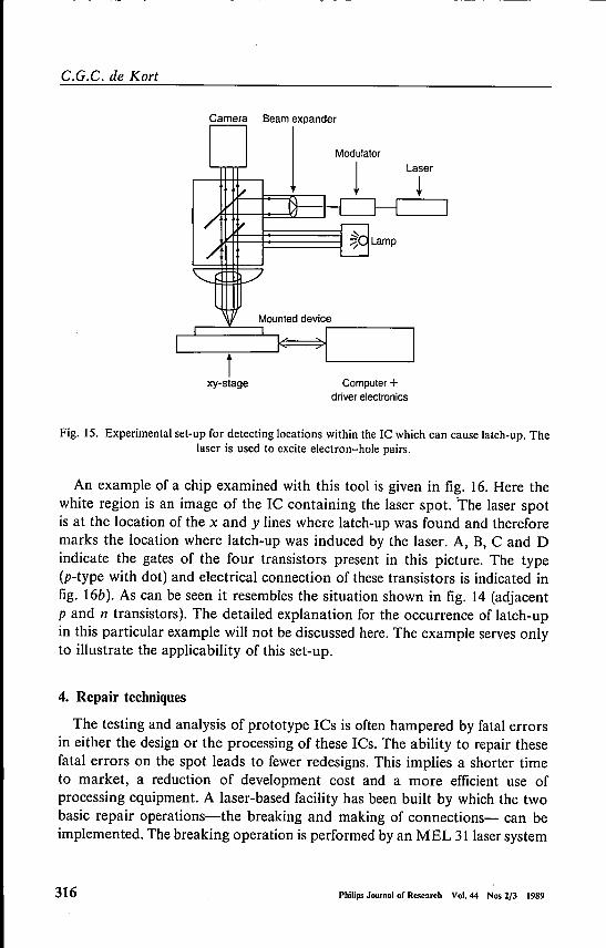
Here we will describe an experimental set-up for detecting sites in an ICwhich are prone to latch-up. This set-up was originally developed by Goossensand van der Wielen 30) and it is used here with some modifications. The basicprinciple is the local creation of electron-hole pairs with a focused laser beam.These electron-hole pairs are separated by the local fields in the IC andconsequently give rise to a small current. The supply voltage is set close toVhigh• When the electron-hole pairs are created in a region sensitive to latch-upthe extra current will trigger latch-up, resulting in a large supply current.
The experimental set-up is given in fig. IS. An He-Ne laser, using amaximum power of 5 mW is focused with a microscope objective to give aspot of 1 J.U11 with an objective with NA = 0.6 (at 50 x magnification). Beforeentering the microscope the laser beam crosses an E-O modulator, to switchthe laser and to adjust the power level, and a beam expander to fill the entrancepupil of the objective. The modulator is used to switch the laser on and offand to adjust the power level. The chip is mounted on a computer-controlledx-y table. To examine the chip the table is scanned in a line-by-line sequence.After each line scan the laser and supply voltage are switched off in order toreset any latch-up condition which might have occurred. The latch-upcondition is determined by measuring the supply current. The scanningdirection is chosen first along the x direction and then along the y direction.The latch-up prone positions are located at the crossings oflines where latch-uphas occurred.
P seosfrate
Philips Journalof Research Vol.44 Nos 2/3 1989 315
C.G.C. de Kort
Camera Beam expander
IMounted device
,.--------,
ixy-stage Computer+
driver electronics
Fig. IS. Experimental set-up for detecting locations within the IC which can cause latch-up. Thelaser is used to excite electron-hole pairs.
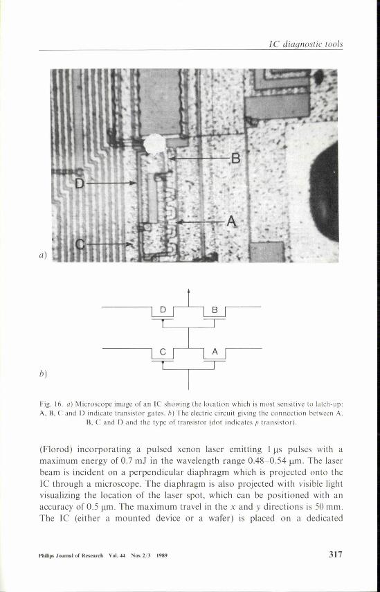
An example of a chip examined with this tool is given in fig. 16. Here thewhite region is an image of the IC containing the laser spot. 'The laser spotis at the location of the x and y lines where latch-up was found and thereforemarks the location where latch-up was induced by the laser. A, B, C and Dindicate the gates of the four transistors present in this picture. The type(p-type with dot) and electrical connection of these transistors is indicated infig. 16b). As can be seen it resembles the situation shown in fig. 14 (adjacentpand n transistors). The detailed explanation for the occurrence of latch-upin this particular example will not be discussed here. The example serves onlyto illustrate the applicability of this set-up.
4. Repair techniques
The testing and analysis of prototype les is often hampered by fatal errorsin either the design or the processing of these ICs. The ability to repair thesefatal errors on the spot leads to fewer redesigns. This implies a shorter timeto market, a reduction of development cost and a more efficient use ofprocessing equipment. A laser-based facility has been built by which the twobasic repair operations-the breaking and making of connections- can beimplemented. The breaking operation is performed by an MEL 311aser system
316 Philips Journalof Research Vol.44 Nos 2/3 1989
Philips Journalof Research Vol.44 Nos 2/3 1989 317
I C diagnostic tools
a)
b)
Fig. 16. a) Microscope image of an IC showing the location which is most sensitive to latch-up:A, B, C and 0 indicate transistor gates. b) The electric circuit giving the connection between A,
B, C and 0 and the type of transistor (dot indicates p transistor).
(Florod) incorporating a pulsed xenon laser emitting Ills pulses with amaximum energy of 0.7 m.I in the wavelength range 0.48-0.54 urn. The laserbeam is incident on a perpendicular diaphragm which is projected onto theIC through a microscope. The diaphragm is also projected with visible lightvisualizing the location of the laser spot, which can be positioned with anaccuracy of 0.5 urn. The maximum travel in the x and y directions is 50 mm.The IC (either a mounted device or a wafer) is placed on a dedicated
C.G.C. de Kort
(x, y, z) stage with a resolution of 0.5 J.ll11 and a maximum travel of 200 mmin both the x and y directions. The x and y motions are computer controlled,which enables automatic die-stepping when using wafers.
When the laser beam is projected withinthe IC the local temperature canrise above the melting or boiling point of the constituent IC materials. Thistemperature increase depends on various parameters: the power density ofthe laser, the absorption coefficient and the thermal conductivity of the chipmaterial. The situation is further complicäted by the presence of severallayers within the IC and by the temperature dependence of the physicalparameters determining the temperature rise. The scratch proteetion (toplayer) is mostly Si3N4 or Siû2, neither of which absorbs at the wavelengthof the xenon laser. Below this layer are aluminium and doped polysilicontracks. The following operations can be performed:
• removal of scratch protection;• removal of aluminium under scratch protection;• removal of polysilicon under scratch protection.
The conditions required for these operations are not dealt with in thispaper.
A supply of material is required for making new connections. This can beachieved by laser-induced liquid-phase metal deposition 31,32). In thisprocess a metal salt solution is used to which ammonia has been added,causing the formation of metal ion complexes. When this solution is appliedon top of the IC, local deposition of the metal can be initiated by localheating with a focused Ar+ laser beam. Within the laser spot thetemperature can be increased to a level where a chemical reaction startswith the net effect that the metal ion complexes decompose and metalatoms are deposited. The local increase in temperature also gives rise tolocal boiling and a stationary jet flow, which result in a very efficientreplenishment of reactants. A very high deposition rate is thereforeachieved. Up to now we have mostly used palladium salt solutions fromwhich palladium tracks are deposited, but the use of other metals is equallypossible 31).
An example taken from ref. 32 is shown in fig. 17. Here the inputprotections of the IC (the meander-like structures) did not function, whichprevented further testing of the device. After bypassing the inputprotections with palladium tracks (black), the devices could be tested andrevealed some design errors! Without this repair these errors would have
318 Philips Joumal of Research Vol.44 Nos 2/3 1989
Philips Journalof Research Vol. 44 Nos 2/3 1989 319
Je diagnostic tools
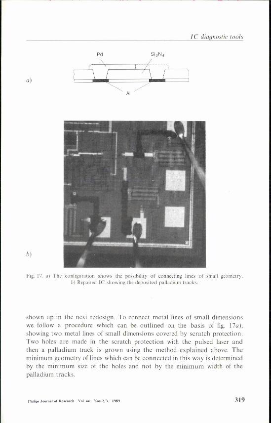
a)
Pd Si3N 4
ó\( ,mTAI
IJ)
Fig. 17. a) The configuration shows the possibility of connecting lines of small geometry.h) Repaired IC showing the deposited palladium tracks.
shown up in the next redesign. To connect metal lines of small dimensionswe follow a procedure which can be outlined on the basis of fig. 17a),showing two metal lines of small dimensions covered by scratch protection.Two holes are made in the scratch proteetion with the pulsed laser andthen a palladium track is grown using the method explained above. Theminimum geometry of lines which can be connected in this way is determinedby the minimum size of the holes and not by the minimum width of thepalladium tracks.
C.G.C. de Kort
5. Comparison and outlook
Up to now we have discussed our own facilities. In this section theperspective is broadened in two ways:
(1) by comparing the diagnostic tools described so far with other existingdiagnostic tools;
(2) by indicating possible developments leading to tomorrow's diagnosticmethods.
Only those diagnostic methods required for obtaining information onelectrically active devices will be considered. The same division of topics asapplied before will be used: in-circuit measurements, in-circuit excitation andin-circuit repair.
5.1. In-circuit measurements
5.1 .1. Fai/ure location
5.1 .1 .1. Liquid crystal studies
As far as temperature resolution is concerned the LC material itself is notthe limiting factor. The temperature resolution is determined by thetemperature regulation and this can be improved to give a higher sensitivityof this method. The spatial resolution is determined by the optics and theheat diffusion in the top layer of'.the IC and the LC. The optical aspect canbe improved by using UV light, but this imposes severe limitations on theclass of suitable LC materials, which must be chemically stable and transparentfor UV illumination.
Voltage measurements can be performed, in the sense that it is possible tosee whether a signal (frequency below 10 kHz) is present or not. This couldbe improved by using faster LC materials or having a better orientation ofthe LC for a better voltage contrast. De voltage contrast will remain difficult,if not impossible, because of the transport of electric charge at the LC-ICinterface, which screens the electric field of the underlying layers. Waveformmeasurements are also possible, in the same way as with E-O sampling. Herethe time resolution remains limited, even if ferroelectric LCs with a switchingtime of 1 JlS are used. In view of the existing trends in ICs, i.e. towards higherspeed and smaller geometries, the most important option is probably theimprovement of temperature resolution. The improvement of voltage contrast,or the capability to measure waveforms, is of value only where other facilities,such as E-beam testing, are not available for performing these measurements.
320 Philip. Journalof Research Vol.44 Nos 2/3 1989
IC diagnostic tools
Improvement of optics is useful for visualizing smaller geometries, but it isdoubtful whether this would give a better indication of the position of theheat source if this source is located beneath the surface.
In any case, LC will continue to be an important tool for determining alocal temperature increase in new generations of ICs. As a diagnostic tool thisoutperforms all the existing methods, such as far-IR and local boiling studies,used for detecting local heat sources within ICs.
5.1.J .2. Light emission
Several improvements are possible in the field of light emission. Aninstrument (Hamamatsu) is currently available on the market which claimsto have reached the ultimate sensitivity by counting the photons emanatingfrom the IC. The photon count is then used to generate a two-dimensionallight emission picture which can be overlaid with a microscope picture ofthe IC.
To expand this method the spectrum of the emitted light can be measured.This would be particularly useful ifa unique relation exists between the emittedspectrum and the mechanism giving rise to light emission. In addition, theimage intensifier can be gated, which opens up the possibility for 'stroboscopic'pictures. Finally, the time dependence of light generated by a chip in pulsedoperation can also be measured in this way. Information thus obtained couldbe valuable for determining characteristic times of charge carriers. Thesedevelopments might be hampered to some extent by the fact that metal linesscreen the light from underlying 'sources'. Of course, close to the screenedsource the light can escape as a result of multiple reflections and this willlimitthe spatial resolution of this technique.
Light emission will remain valuable for future generations of ICs in thesense that it gives the coordinates of the fault location directly. It is ourexperience that light emission is often complementary to LC studies: whenheat is generated no light emission occurs (e.g. a polysilicon short), and theconverse also applies (e.g. hot electrons). Sometimes, however, both effectsoccur simultaneously (e.g. a gate oxide with a current of 10 J.LA). The best wayto achieve an improvement is to find and understand the various mechanismsgiving rise to light emission in a working IC.
5.J .J .3. Electron beam techniques
E-beam techniques seem to have come to maturity over the last year or so;several integrated systems have already reached the market place. Theintegration refers to the connection of an electric tester, as the source of
Philips Journalof Research Vol.44 Nos 2/3 1989 321
C.G.C. de Kort
electrical signals, to the E-beam tester and the coupling between the layouton a work station and the voltage contrast picture of the E-beam tester. Thistype ofintegration reconciles the requirements ofbeing user-friendly and useful,but this aspect will not be discussed here.
Let us now return to the core of E-beam testing. For voltage contrast aresolution of 0.1 f.U11 can be achieved, though at the expense of a lower primarybeam current. This problem has been tackled by Frosien and Plies 33), whodesigned a new electron optic column, optimizing the primary beam currentat a given spot size. On the detection side it is possible to improve thesignal-to-noise ratio of the detector or to use image processing. The latteroption is included in modern E-beam testers. In this way voltage contrastimages can be improved, which will help in locating errors. This part ofE-beamtesting will no doubt continue to be a very useful diagnostic tool.
5.J.2. Waveform measurements
5 .J.2.J. Electron beam techniques
In considering waveform measurements the time resolution is determinedby the blanking time. At present the lower limit is around 100 ps. This canbe improved by faster electronics or by using other methods which will bediscussed below. Though the prospects for these stand-alone methods may befavourable, the required degree of integration can be obtained only after a lotof work.
The use of shorter blanking times results in a very low average SE current.Horstman attacks this problem by introducing a new detection method basedon counting è"). In our laboratory we will follow this line of thought anddesign a specially built detection arrangement to exploit the counting idea tothe full. Once proven, this method will be valuable for all systems detectingpulsed SEs. The voltage resolution is directly proportional to thesignal-to-noise ratio in the detection system, and both an increase in theprimary beam current and a better detection method (increasing the signaland/or decreasing the noise) will increase the voltage resolution. As explainedabove, the voltage accuracy depends on a number of parameters. Importantfactors which deserve consideration in existing and future systems are thebeam-pointing stability and changes in the SE yield caused by influences otherthan the voltage to be measured.
5.1.2.2. Electro-optic sampling
The time resolution of E-O sampling can be as low as 0.3 ps 19). In ref. 19the LiTa03 and the geometry. used limit the time resolution. For the near
322 Philips Journalof Research Vol.44 Nos 2/3 1989
I C diaqnostic tools
future a time resolution of 50 ps would seem to be satisfactory for measuringsilicon les. It is therefore possible to use semiconductor lasers capable ofdelivering pulses of 50 ps or less 35). This field has been explored by Valdmanisand Pei 37) and Nees and Mourou 36). As regards measurements in siliconles, several complications arise. First, the duration of the electrical signal isfairly long compared with the pulse width of the laser. This means that theaverage signal (as with E-beam testers) becomes rather low. This averagesignal is proportional to the average laser power, the magnitude of the E-Oeffect and the detector sensitivity. The noise in the signal is determined by thenoise in the laser 21) and noise in the detectors. Here materials with a higherE-O effect would, of course, be highly desirable.Another complication is caused by the delay. The signal can be delayed
with respect to the laser pulses (electronic), or the laser pulses can be delayedwith respect to the signal (both optical and electronic). Seen from theperspective of existing test systems it would be most convenient to delay thelaser pulses with respect to the signal. This means that the laser must betriggered by a signal, derived from the tester, which is variable in frequency.In the case of semiconductor lasers this is a straightforward process, but withmode-locked or colliding pulse mode (ePM) lasers it is impossible. In thelatter case a trigger signal must be derived from the laser pulses. Whensemiconductor lasers are used the time resolution will be limited by jitter inthe laser driving signal, jitter in the delay and the laser pulse width. Anotherway to circumvent triggering problems with the laser is to use a continuousworking laser and very fast detectors. The triggering must then be done inthe detector chain. At present this method lacks sensitivity because of thelower sensitivity of fast detectors.The spatial resolution of this method is determined by the wavelength and
the optics. Most experiments have been done in the IR region withsemiconductor lasers or in the visible region with mode-locked and ePMlasers. Decreasing the wavelength (by frequency doubling) could be a feasiblealternative for increasing the spatial resolution. This also imposes somerestrictions on the suitable E-O materials since a number of them are lesstransparent towards the UV region.
5.1.2.3. Photoelectron scanning electron microscopy
The photoelectron scanning electron microscope 38) operates in the sameway as a normal E-beam tester. The only difference is that the primary beamis generated by a picosecond laser pulse in the UV region. This laser pulse isfocused on a gold film and liberates the photoelectrons which make up the
Philips Journalof Research Vol.44 Nos 2/3 1989 323
C.G.C. de Kort
mary beam. The advantage here is that one gets a higher (pulsed) currentdensity of the primary E-beam and the blanking action is performed by thelaser pulses, which allow a time resolution of 5 ps. The spatial resolution isaround 0.1 J.LIll and the voltage resolution is better than that for normal E-beamtesting because of the higher primary beam current. As regards triggering, thesame considerations apply as in the case of E-O sampling.
5.1.2.4. Photoemission
In the photoemission technique 39) UV laser pulses are used togenerate photoelectrons directly from points within the chip. Thesephotoelectrons are then selected and detected in the same way as in E-beamtesting. Here one has the advantage of a higher (pulsed) SE current as wellas very good time resolution. The spatial resolution is determined by theoptics and wavelength and amounts to 0.5 J.U11. Again the considerations withrespect to triggering apply.
5.1.2.5. Photoconductive sampling
Photoconductive sampling relies on very fast switches driven by picosecondlaser pulses 40). These switches link the measuring point to a point electricallyconnected with the outside world. The switches enable waveforms with a timeresolution of 1ps to be sampled. A voltage resolution of 1mV with anintegration time of 300 ms has been proven 40). This method is limited to thoseapplications where it is known in advance where the measurements are to bedone.
Comparing the various waveform measurement techniques, it is clearthat in order to reach picosecond time resolution laser-based systems(Secs 5.1.2.2-5.1.2.5) are required. When these systems must be interfacedwith testers several difficulties are predictable. These difficulties are avoidedwhen a laser-based test system 41) is used. If a time resolution of around 50 psis considered sufficient, E-O sampling with semiconductor lasers can beemployed. Interfacing with testers then poses no special problems.Conventional E-beam systems employing a faster beam blank driver couldalso be used. An advantage of E-O sampling over E-beam testing is that theformer can be done in air, while the latter has to operate in vacuum. Theadvantage of E-beam testing is its superior spatial resolution, which will beimportant in future generations of chips. Waveform measurements on futureICs will therefore probably show the merging of a laser-based approach, toachieve good time resolution, and E-beam testing, giving good spatial
324 Philips Journalof Research Vol. 44 Nos 2/3 1989
IC diagnostic tools
resolution. At present the photoelectron scanning electron microscopy comesclose to this situation.
5.2. In-chip excitation
Cl. Particle sensitivity will remain an issue for the future generations ofmemories. This statement is based on the fact that both the node capacitanceand node voltage will be lower for smaller geometries. More simulation workwill thus be required, but basically the measurements will be carried out inthe same way.
Latch-up detection can be performed at other wavelengths but no essentiallynew developments are to be expected here. In circuits with smaller geometriesand multiple metal layers it will become exceedingly difficult to reach thediffusion layers.
OBlC and EBIC are diagnostic methods, also employing in-chip excitation,which measure the changes in supply current caused by either an optical beam(OBIC) or an E-beam (EBIC). They can be useful for the detection of faultsin special applications (p-njunctions) and larger geometries, where the excitingbeams can easily reach the sensitive layers. Widespread applicability of thesetechniques is not to be expected.
5.3. I n-CÎrcuit repair
Repair based on laser systems has the disadvantage of a fairly limited spatialresolution. The most appropriate technique for increasing resolution is theuse of focused ion beams. Cutting with a focused ion beam has already beenshown to give a spatial resolution of 0.1 J.U1142). A further advantage of thismethod is its greater controllability and selectivity. This allows holes to bemade in one layer without damaging neighbouring layers, which opens up thepossibility of making connections to underlying layers. However, thedeposition of conductive material still presents some problems. At present,deposition is still mostly performed by the decomposition of (toxic) gases,which leads to complicated hardware. The development of alternativedeposition methods seems important.
Acknowledgements
It is with great pleasure that I acknowledge the many discussions with GidiFleuren. He also introduced me to the world of Le and helped me with thefirst set-up. I would like to thank Gert 't Hooft for his cooperation with E-Osampling. Without the help and persistenee of Andre van der Putten,
Philips Journalof Research Vol.44 Nos 2/3 1989 325
326 Philips Journalof Research Vol.44 Nos 2/3 1989
C.G.C. de Kort
Jan Jacobs and Jan Rikken, repair would not have been possible. Thediscussions with Rob Horstman are gratefully acknowledged. Finally, I wouldlike to thank Paul Damink and Joris Vrehen for their indispensable help andcontinuous support.
REFERENCESI) G.H. Heilmeier, L.A. Zanoni and L.A. Ba r-t o n, IEEE Trans. Electron. Devices, 17,
22 (1970).2) J.L. Lanning, Appl, Phys. Lett., 21,173 (1972).J) D.J. Channin, IEEE Trans. Electron. Devices, 21, 650 (1974).4) E. M. Fleu ren, Proc. 21st Int. Reliability Physics Symp., Phoenix, AZ, U.S.A., 1983, IEEE,
~ ~S)d~~'ä~~~~t~~~c~·~V~"iï,proc. i2""'n-d":C·-:-ln-t-.="R--:el7'ia":"bC7ih'·-ty-=P-:"'h-ys""i-cs-S=-y-m-p-.-,L::-a-s'":V~e-g-a-s,'":N~E-,::-:U:-:.S::-.A~.,--~I1984, IEEE, New York, 1984, p. 119.
6) R. Weyl, B. Lisch ke, R. Kappelmeyer and F. Beck, Mitteilungen aus den ForschungsLaboratorien und dem Werk für Bauelemente, Siemens AG, Munich, 1985, p. 1.
7) F. Beck, Elektronik, 13,82 (1986).8) P. Hendriks, K. de Kort, R.E. Hortman,J.-P. Andre, C.T. Foxonand 1. Wolter,
Semicond. Sci. Techno!., 3,521 (1988).9) N. Khurana and C.-L. Chiang, Proc. 25th Int. Reliability Physics Symp., San Diego,
CA, U.SA, 1987, IEEE, New York, 1987, p. 72.10) C.W. Oatly and T.E. Everhart, J. Electron., 2,568 (1957).I I) G. V. Luk ia n 0 ff and T. R. To uw, Proc. Conf. on Scanning Electron Microscopy, Chicago,
IL, 1975, p. 615.12) W. Argyo, H.- D. Brust, 1.Otto, E. Plies and E. Wolfgang, Siemens Forsch. Entwick.
Ber., 14,216 (1985).IJ) R. Horstman and F. Lier, Philips Research Laboratories, personal communication.14) P. Fazekas, H.-P. Feuerbaum and E. Wolfgang, Electronics, 105 (July 1981).IS) O.W. Ranasinghe, 0.1. Machinand G. Proctor, Microelectron. Eng.,7,397 (1987).16) F. Agricola, Philips Research Laboratories, personal communication.17) S. Gorlich, P. Kessler and E. Plies, Microelectron. Eng., 7,147 (1987).18) K.O. Herrmann and E. Kubalek, Microelectron. Eng., 7, 405 (1987).19) J.A. Valdmanis, Electron. Lett., 23, 1308 (1987).20) R.K. Jain, Test and Measurement World, 4, 40 (June 1984).21) B.H. Kolner and O.M. Bloom, IEEE J. Quantum Electron., 22, 79 (1986).22) J.A. Valdmanis and G. Mourou, IEEE J. Quantum Electron., 22, 69 (1986).2J) G. Mourou, Characterization ofVery High Speed Semiconductor Devices and Integrated
Circuits, ed. Ravi Jain, in Proc. Soc. Photo-opt. Instrum. Eng., 795, 300 (1987).24) B. Couillard, V. Fossati-Bellani and G. Mitchell, Proc. Ultrashort Pulse
Spectroscopy and Applications, Los Angeles, CA, U.S.A., in Proc. Soc. Photo-opt. Instrum.Eng., 533, 46 (1985).
25) T.C. May and M .H. Woods, IEEE Trans. Electron. Devices, 26, 2 (1979).26) K. de Kort and P. Damink, Philips Research Laboratories, personal communication.27) S. W. Heidmiller, C.G .C. de Kort and F.J. List, Philips Research Laboratories,
personal communication.28) R.R. Troutman (ed.), Latehup in CM OS Technology, Kluwer, Dordrecht, 1986.29) R. Goossens, Philips J. Res., 44,241 (1989).JO) R. Goossens and 1. van der Wielen, Philips Research Laboratories, personal
communication.31) A.M.P. van der Putten, J.W.M. Jacobs, J.M.G. Rikken and C.G.C. de Kort,
Laser Assisted Processing, eds D. Laude and G. Rauscher, Proc. Soc. Photo-opt. Instrum.Eng., 1022, 71 (1989). •
32) K. de Kort, Philips Research Laboratories, personal communication.JJ) 1. Frosien and E. Plies, Microelectron. Eng., 7, 163 (1987).J4) R.E. Horstman and F.J. Lier, Microelectron. Eng., 7, 209 (1987).
IC diagnostic tools
35) K. Ketterer, E.H. Bottcher and D. Bimberg, App!. Phys. Lett., 50(21),1471 (1987).36) J. Nees and G. Mourou, Electron. Lett., 22(17),918 (1986). .37) J.A. Valdmanis and S.S. Pei, Proc. Conf. on Picosecond Electronics and Optoelectronics,
Incline Village, U.S.A., January 14-16, 1987, Springer, New York, 1987, pp. 14-16.38) P. May, J.-M. Halbout and G. Chiu, in Characterization of Very High Speed
Semiconductor Devices and Integrated Circuits, ed. Ravi Jain, Proc. Soc. Photo-opt. Instrum.Eng., 795, 201 (1987).
39) A. Blacha, R. Clauberg, H. Seitz, W. Wolz and H. Beha, in Characterization ofVery High Speed Semiconductor Devices and Integrated Circuits, ed. Ravi Jain, Proc. Soc.Photo-opt. Instrum. Eng., 795, 286 (1987).
40) J.-M. Halbout, P. G. Mayand M.B. Ketchen,inCharacterizationofVeryHighSpeedSemiconductor Devices and Integrated Circuits, ed. Ravi Jain, Proc. Soc. Photo-opt. Instrum.Eng., 795, 247 (1987).
41) F.J. Henley and Hee-June Choi, Proc. IEEE International Test Conf., Washington, DC,U.S.A., 1988, Computer Society Press of IEEE, Washington, DC, 1988, p. 700.
42) R. Clampitt, R. Watkins and J. Whitaker, Microelectron. Eng., 6, 605 (1987).
AuthorKees de Kort: Ph.D. (Physics), University of Nijmegen, The Netherlands, 1979; PhilipsResearch Laboratories, Eindhoven, 1979- .The topic ofhis thesis was the interaction offar-IRlight with superconductors (mercury) and with MgO crystals containing iron and chromiumimpurities. At Philips he studied electrical conduction mechanisms, particularly electronlocalization and electron-electron interaction, in thin ruthenium and Ru02 films and in thickfilms containing conductive ceramic materials. In 1986 he became a member of the IC DesignCentre, where he studies and develops methods suitable for performing diagnostics in integratedcircuits.
Philips Journalof Research Vol.44 Nos 2/3 1989 327