innovative nano and micro technologies for …...• graphene-based coating/adhesive o graphene chip...
TRANSCRIPT

Innovative Nano and Micro Technologies for Advanced Thermo and Mechanical Interfaces
NANOTHERM
Large-Scale Integrating Project Start Date : 0 1/09/12 Project n° 318117 Duration : 36 months THEME 3 : Information and Communication Technologie s
WORK PACKAGE 5 : Project demonstrators and Systems Integration
DELIVERABLE D5.1 Report on first selected technologies
for demonstrators
Due date : T0+12 Submission date : T0+12
Lead contractor for this deliverable : IFX/Bosch
Dissemination level : CO
Ref. Ares(2014)558307 - 03/03/2014

D5.1
2/42
WORK PACKAGE 1: Systems and Applications Specifications
TASK 5.1/5.2
Selection of the demonstrators and technologies Adaptation of processing technologies suitable for developed materials
PARTNERS ORGANISATION APPROVAL
Name Function Date Signature
Prepared by: Klaus-Volker Schuett
2013-08-26
Approved by:
CHANGE RECORD SHEET REVISION LETTER DATE PAGE NUMBER DESCRIPTION
Template 15/11/12
Draft 06/08/2013
First Version 26/08/2013
Second Version 27/08/2013 Viking contribution added

D5.1
3/42
CONTENTS
1 ABBREVIATION / DEFINITION ......................... ........................................................................... 5
1.1 DEFINITION OF INTERCONNECT TECHNOLOGIES .......................................................................... 6
1.2 DEFINITION OF SYSTEMS ........................................................................................................... 7
2 INDUSTRIAL DEMONSTRATORS .......................... ..................................................................... 8
2.1 AVIONICS DEMONSTRATOR (THALES) ......................................................................................... 9
2.1.1 Objectives ......................................................................................................................... 9
2.1.2 Application ........................................................................................................................ 9
2.1.3 Lay-out/Materials .............................................................................................................. 9
2.1.4 Requirements ................................................................................................................. 10
2.1.5 Pre-Selected Materials and Technologies ....................................................................... 10
2.1.6 First Test Results ............................................................................................................ 10
2.2 LIGHTING DEMONSTRATOR (PHILIPS)........................................................................................ 12
2.2.1 Objectives ....................................................................................................................... 12
2.2.2 Application ...................................................................................................................... 12
2.2.3 Lay-out/Materials ............................................................................................................ 12
2.2.4 Requirements ................................................................................................................. 13
2.2.5 Pre-Selected Materials and Technologies ....................................................................... 14
2.2.6 Test Results TIM ............................................................................................................ 15 2.2.6.1 First batch .................................................................................................................................................... 15 2.2.6.2 Second batch .............................................................................................................................................. 16
2.2.7 First Results Laminated Leadframe Concept .................................................................. 17
2.3 AUTOMOTIVE DEMONSTRATOR (BOSCH) ................................................................................... 18
2.3.1 Objectives ....................................................................................................................... 18
2.3.2 Application ...................................................................................................................... 18
2.3.3 Lay-out/Materials ............................................................................................................ 19
2.3.4 Requirements ................................................................................................................. 20
2.3.5 Pre-Selected Materials and Technologies ....................................................................... 21
2.3.6 First Test Results ............................................................................................................ 21
2.4 MULTIMARKET DEMONSTRATOR (INFINEON) ............................................................................. 23
2.4.1 Objectives ....................................................................................................................... 23
2.4.2 Application ...................................................................................................................... 23
2.4.3 Lay-out/Materials ............................................................................................................ 24
2.4.4 Requirements ................................................................................................................. 24
2.4.5 Pre-Selected Materials and Technologies ....................................................................... 25
2.4.6 First Test Results ............................................................................................................ 26
2.5 RELIABILITY DEMONSTRATOR (VIKING) ..................................................................................... 31
2.5.1 Objectives ....................................................................................................................... 31
2.5.2 Application ...................................................................................................................... 32
2.5.3 The measurement technique .......................................................................................... 33
2.5.4 Requirements ................................................................................................................. 34 2.5.4.1 Requirements against the other demonstrators ........................................................................................... 34 2.5.4.2 Requirements against the semiconductor structures used by the Viking demonstrator............................... 37
2.5.5 Features of the main control software ............................................................................. 37
2.5.6 References ..................................................................................................................... 38
2.6 WAFER LEVEL PACKAGING DEMOSNTRATOR (NANIUM) .............................................................. 39
2.6.1 Objectives ....................................................................................................................... 39
2.6.2 Application ...................................................................................................................... 39
2.6.3 Lay-out/Materials ............................................................................................................ 39
2.6.4 Requirements ................................................................................................................. 40

D5.1
4/42
2.6.5 Pre-Selected Materials and Technologies ....................................................................... 41
2.6.6 Initial Results, Sub-system 1 ........................................................................................... 41
FIGURES
Figure 1: Schematics of avionics demonstrator. 10
Figure 2: TIM with VACNT in avionics demonstrator. 10
Figure 3: Luxeon Z power LED package. 12
Figure 4: Schematic lay-out of demonstrator (not to scale). 13
Figure 5: Dimensions of Luxeon-Z package (left) and Figure 6: Luxeon-Z pad lay-out (right). 13
Figure 7: Laminated leadframe on PCB concept. 14
Figure 8: Sintering profile for sinter paste demonstrator (Heraeus). 15
Figure 9: Cross-sectional schliffs of first samples. 16
Figure 10: Cross-sectional schliffs of SSA7-859 (top) and SSA7-889 (bottom). 16
Figure 11: Thermal results for different board concepts. 17
Figure 12: Electric power steering concept. 19
Figure 13: Electrical power steering unit. 19
Figure 14: Schematic of Bosch demonstrator. 19
Figure 15: Lay-out of automotive demonstrator. 20
Figure 16: Lay-out of Bosch sub-system sample. 20
Figure 17: Typical power management & multimarket application examples: wind power, lighting, solar energy, power supplies, DC-DC converter etc. 23
Figure 18: Multimarket demonstrator. 24
Figure 19: Multimarket subsystem. 24
Figure 20: Dispensing pattern fabricated by the ESEC 2008 equipment at IFX Regensburg. 26
Figure 21: Die placement with ESEC 2008 equipment at IFX Regensburg. 27
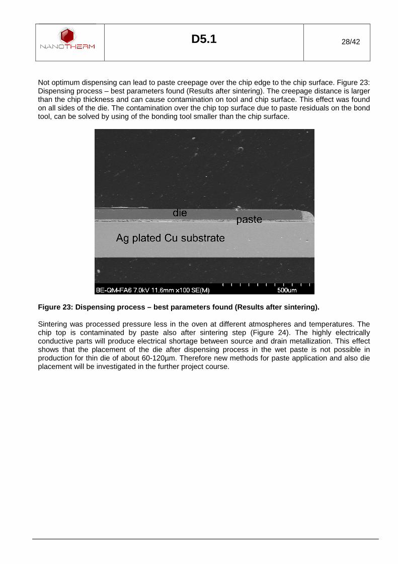
Figure 22: Dispensing process – not sufficient volume of the paste dispensed (Results after sintering). 27
Figure 23: Dispensing process – best parameters found (Results after sintering). 28
Figure 24: Results after sintering. 29
Figure 25: Shear strength measurements for investigated pastes depended of sintering conditions (source: project partner Heraeus). 29
Figure 26: Shear strength measurements for investigated pastes depended of bond line thickness (BLT) (source: project partner Heraeus). 30
Figure 27: General flowchart of reliability testing. 31
Figure 28: LED LM80 life-time test measurement results. a) lumen maintenance results, b) Pre- and post stress test results. 32
Figure 29: Junction-to-X thermal resistance calculated from a temporal difference of the junction temperature and the power dissipated in the device. 33
Figure 30: The basic scheme of thermal transient testing based on JEDEC JESD51-1 [2] and JESD51-14 [3]. 34
Figure 31: The scheme of increased throughput thermal testing multiple PN junctions (e.g. LEDs) connected in series. 35
Figure 32: The possible realization of the thermal reliability testing principle in the Viking demonstrators (shown for the example of a column of 8 LEDs). 36
Figure 33: The setup panel of the reliability demonstrator control software. 37
Figure 34: Power eWLB layout. Top left: stack build-up; Right: topview of heating array; Bottom left: two sub-systems, for mold compound and TIM application development 40
Figure 35: Power eWLB target requirements 40

D5.1
5/42
TABLES
Table 1: Requirements avionics demonstrator. 10
Table 2: Requirements lighting demonstrator. 14
Table 3:Shear strength results for first samples. 15
Table 4: Requirements of Bosch demonstrator. 21
Table 5:Shear strength results for first samples. 22
Table 6: Requirements of IFX demonstrator (defined in WP1). 25
Table 7: Requirements Power eWLB demonstrator. 40
Table 8: Results of addition of 0.2%graphene to MC2. 41
Table 9: Thermal resistance results of the several variants of subsystem1. 42
1 ABBREVIATION / DEFINITION
Throughout the project the following definitions are used.

D5.1
6/42
1.1 DEFINITION OF INTERCONNECT TECHNOLOGIES
In between brackets the supplier is indicated: • VACNT- Vertically Aligned Carbon Nano Tubes (SHT, TRT) • Sintered adhesive or nano-adhesive (Heraeus, AMEPOX, Chalmers):
o Polymer matrix highly filled with micro and nano-particles (e.g. Ag). o Polymer matrix remains in structure adding significant properties to the final interconnect. o Processing: Pressureless sintering.
• Sintered paste or nano-paste material (Heraeus, AMEPOX, Chalmers): o Sintered metallic micro- and nano-particles mixture (e.g. Cu or Ag). o Polymer is used to make the paste processable, so it does not significantly contribute to
the properties of the final interconnect (it mostly vanishes due to processing). • Graphene-based coating/adhesive
o Graphene chip coating o Graphene filler sheets in adhesive matrix along with micro-Ag flakes
• Silver coated nano-SiC particles in adhesive matrix
D5.1
7/42
1.2 DEFINITION OF SYSTEMS
• Demonstrator: The final system to show capability of thermal interface technology on application level.
• Subsystem: The simplified demonstrator which is used to investigate a specific physical function. • Test sample or sample: Any specific thermal interface material (TIM) that is used for
characterization purposes.

D5.1
8/42
2 INDUSTRIAL DEMONSTRATORS
Five demonstrators are defined in this document (please see also D1.2). The avionics, lighting, automotive and multimarket demonstrators show the ability of the interconnect technologies developed. These demonstrators are referred to as application demonstrators. The reliability demonstrator shows the reliability test platform. The demonstrators are outlined in this section.

D5.1
9/42
2.1 AVIONICS DEMONSTRATOR (THALES)
2.1.1 Objectives
Trends in radar detection and electronic warfare for avionics and airborne applications are driven by the use of multifunctional antennas for fighter aircrafts or drones, the search for lighter and more compact antennas architectures, and by the introduction of new high power density technologies such as GaN and MEMS. As an example, in radar applications, high dissipative components such as High Power Amplifiers (HPA) are well known, and current publications have already highlighted the difficulties to cool them down. For future applications, GaN HPA requires optimized innovative solutions. New improved Thermal Interface Material (TIM) will participate into the success of the introduction on the market of innovative technologies. The management of the temperature at the interface in an aerospace environment is necessary to control junction temperature and therefore improve reliability.
2.1.2 Application
The HPA (High Power Amplifier) demonstrator is aimed to evaluate the performance of new high performing TIM in a THALES representative application, i.e. an X-band RF power amplifier. Two thermal interfaces are to be tested and implemented: between the HPA die and the chip case (TIM1), and between the chip case and the heat spreader (TIM2).
2.1.3 Lay-out/Materials
RF Modules will integrate the TIMs. The modules are designed to allow temperature measurement of functioning chips. A cross section of the module is shown in Figure 1.
RF End Launch connector
Pipe for water circulation
Cover
PCB Frame
Heat sink thermal sensor
Heat sink
Copper substrate
MMIC
Internal Side View
Interfaces close-up
Aluminum Heat sink
Copper substrate
TIM 1
TIM 2
MMIC 10 ∼ 50 µm
∼ 100 µm

D5.1
10/42
Figure 1: Schematics of avionics demonstrator.
2.1.4 Requirements
Most of the requirements pertain to the TIM1 material as it is the most critical interface as being the closest to possible hot spots.
Table 1: Requirements avionics demonstrator. TIM1 TIM2 Thermal conductivity >25 >15 Electrical conductivity Not required Life Time >1000h / 125°C N/A Thermal shock 500 cycles -55°C /125°C N/A Environment 1000h 85°C/85%RH N/A
2.1.5 Pre-Selected Materials and Technologies
The material of choice for the avionics demonstrator is the interface based on vertically aligned carbon nanotubes (VACNT) for TIM1 application. Ideally, CNTs are grown directly on the cold plate which will then be integrated in the packaging. However, the cold plate assembly may not withstand the growth conditions of the CNTs (high temperatures). In that case, CNTs have to be grown on a substrate with high thermal conductivity, and possible to be integrated in the interface using an additional interface material i.e. solder. Foreseen typical implementation includes growth of CNT on a copper substrate, soldering of the copper substrate on the cold plate, deposition of the interface material (polymer or gold thin film), and finally interface closing.
Figure 2: TIM with VACNT in avionics demonstrator. The final bonding strength of the interface relies on substrate – cold plate adhesion (via solder), CNT-growth substrate bonding and gold or polymer bonding of CNT tips on the chip’s backside.
2.1.6 First Test Results
Growth of VACNT was performed directly on copper substrates, in order to evaluate their thermal performance. However the quality of the mats was not at the level of the ones grown on Silicon. It is a generally admitted idea that quality growth on metal is hindered by interdiffusivity issues with the catalyst, and by a degradation of the surface roughness at high temperature. Therefore, the quality and density of the carbon nanotubes is affected.
Chip Solder
Copper substrate
Cold plate
VACNT

D5.1
11/42
A new technology is being investigated were the mats are directly transferred onto a copper substrate with a metallic interface and according to a method developed by SHT.

D5.1
12/42
2.2 LIGHTING DEMONSTRATOR (PHILIPS)
2.2.1 Objectives
The thermal performance of current LED devices is a strong limiting factor in achieving high operating temperatures and high power densities, which are essential requirements for future LED applications. The goal of the lighting demonstrator is to prove that a combination of new substrate technologies and thermal interface materials makes it possible to handle the expected high heat flux densities in ceramic or leadframe LED packages while maintaining or even improving performance and lifetime of the LED system.
2.2.2 Application
The intended lighting demonstrator is based on the Luxeon-Z power LED package (see Figure 3). This small power package is used for customized multi-chip and multi-colour light sources.
Figure 3: Luxeon Z power LED package.
2.2.3 Lay-out/Materials
The Luxeon-Z surface mounted package consists of an LED die on a ceramic substrate with NiAu finished copper terminals on the bottom side. The demonstrator aims to show the best interconnect solution of this package to a substrate trading-off thermal, electrical, reliability, and manufacturability aspects as a result of the Nanotherm project. The schematic lay-out of the demonstrator is shown in Figure 4 and detailed dimensions are shown in Figure 5. A typical bond line thickness of currently used SnAgCu (SAC) materials is 60 µm. Depending on the project findings the BLT of the demonstrator can be redefined. The solder pad design of the substrate is given in (left) and Figure 6. The demonstrator will eventually be compared to the current state of the art which is comprised of the

D5.1
13/42
Figure 4: Schematic lay-out of demonstrator (not to scale). Luxeon-Z LED package attached to an Insulated Metal Substrate (IMS) board by lead-free tin-silver-copper (SAC) solder material.
Figure 5: Dimensions of Luxeon-Z package (left) and Figure 6: Luxeon-Z pad lay-out (right).
2.2.4 Requirements
The requirements for the lighting demonstrator are listed in Table 4. Additionally, as the two terminals of the lighting demonstrator should be electrically separated it is required to reach a fine-pitch spacing of 0.2 mm. Of course the final interconnect technology should also be fully ROHS compliant.

D5.1
14/42
Table 2: Requirements lighting demonstrator.
2.2.5 Pre-Selected Materials and Technologies
The following sintered materials were pre-selected for the lighting demonstrator: • SSA7-899-series (Sinter Adhesive Heraeus)
• SSA7-859-series (Sinter Adhesive Heraeus)
• LTS295-series (Sinter Paste Heraeus)
As a possible low-cost alternative for the state-of-art IMS board, a laminated leadframe concept functioning as heat spreader attached to a low-cost PCB is considered. The PCB requires copper vias to extract the heat to the bottom of the PCB which serves as a heat-sink. The concept is shown in Figure 7.
Figure 7: Laminated leadframe on PCB concept.
Thermal Conductivity TIM [W/mK] 20
Electrical Resistivity [Ohm cm] <20e-5
Max. overall VF 240 V
Max. IF 2 A
Life Time >1000h / 150°C
Preconditioning MSL1
Process Temperature <=260°C
Cure time < 30 min
Pressure 0 kPa

D5.1
15/42
2.2.6 Test Results TIM
2.2.6.1 First batch
Initial samples of the Luxeon-Z package on NiAu finished DCB with sinter adhesive and sinter paste were prepared by Heraeus. The sinter adhesive was sintered at 200°C for 30 minutes. The sinter paste was sintered by a more complicated profile which is indicated in Figure 8.
Figure 8: Sintering profile for sinter paste demons trator (Heraeus).
Table 3:Shear strength results for first samples.
Shear tests were performed on these samples. The shear results are indicated in Table 2. Clearly, the adhesion at 25°C of the sinter adhesives (SSA) show ed much better results than the sinter paste results. The results at 260°C, however, are not ver y distinctive. Also, cross-sections of the resulting samples were prepared as shown in Figure 9.
Shear strength @25°C
Shear strength @260°C
LTS295-26P2 4.5 N/mm2 4.9 N/mm2 SSA7-859230 20.5 N/mm2 2.9 N/mm2 SSA7-899456 37.4 N/mm2 4.9 N/mm2

D5.1
16/42
Figure 9: Cross-sectional schliffs of first samples .
2.2.6.2 Second batch
In the next stage, samples were created at Philips. Only the sinter adhesive materials were tested as these showed most promising results. The sinter adhesives were used to mount a ceramic test component (1.8 mm x 3.4 mm x 0.5 mm) with silver finished copper pads onto an Al-IMS substrate with silver finished copper tracks. As before, pressureless sintering was performed at 200°C for 30 minutes. Assembly was done manually on a FineTech placer before sintering. Slight placement pressure was used on the component to ensure contact. This results in a very thin bond line of approximately 11-13 µm as shown by the cross-sections shown in Figure 10. Also, the adhesive is pushed out of the pad area. In contrast to the SSA7-859 result, the SSA7-889 result showed several voids in the connection. These samples were also subjected to a shear test. The average shear strength for SSA7-859 and SSA7-889 were 31 N/mm2 and 34.5 N/mm2, respectively. Differences with the previous measurement can be contributed to e.g. pad finish, pad dimension, BLT, and the extended connection outside the pad areas. In future work, focus is on control of placement force, bond line thickness and squeeze out and optimization of the sintering profile.
Figure 10: Cross-sectional schliffs of SSA7-859 (to p) and SSA7-889 (bottom).

D5.1
17/42
2.2.7 First Results Laminated Leadframe Concept
Laminated leadframes are manufactured by Stamped Circuit Board (SCB) technology. In this manufacturing process, a glass reinforced epoxy resin foil or a similar dielectric layer like Polyimide foil and a copper sheet are initially structured and processed separately. Subsequently, a laminating process joins the materials with high positioning accuracy. The thermal resistance of the lighting demonstrator is influenced by the thermal conductivity of the used materials as well as the heat spreading area of the heat transiting elements of the system. It is targeted that, with a heat spreader on a low-cost PCB, a cost-competitive solution for the state-of-art expensive IMS or Metal Core Printed Circuit Board (MCPCB) can be developed without loss of thermal performance. Thermal simulations were done at Heraeus to estimate the thermal performance of the laminated leadframe concept. Three different heat spreader configurations were considered. The effective copper pad area (3 mm x 3 mm, 5 mm x 5 mm), and presence of vias in the PCB were varied. Results are compared to results without heat spreader (component on PCB) and with IMS. The simulations (see Figure 11) show that an improvement of the thermal resistance as well as a reduction of the junction temperature is possible using a heat spreader on top of the PCB. A PCB with thermal vias in combination with a 3x3mm heat spreader shows competitive results to the IMS board.
Figure 11: Thermal results for different board conc epts. In the next step, a cost analysis (materials, processes, assembly.…) of the laminated leadframe concept will be performed comparing to the IMS solution. If the laminated leadframe indeed shows out to be cost competitive, samples and packed systems will be tested to investigate the reliability properties of the laminated leadframe concept.

D5.1
18/42
2.3 AUTOMOTIVE DEMONSTRATOR (BOSCH)
2.3.1 Objectives
Electronic systems are enabler for new functions like safety, engine management, exhaust treatment and comfort in cars. Share of electronic systems in modern cars is expected to increase up to 35 % of overall costs within the next few years. Driving forces in automotive electronics are:
• Smaller housings of controller units for any aggregate. • System integration (die shrinkage, mechatronic modules, improved functions). • Position of electronic components closer to mechanic and/or heat dissipating components
(harsh environment). • Higher power consumption of electronic modules like x-by-wire systems, power converters for
hybrid cars and electric cars.
This leads to higher power consumption on smaller areas and elevated heat sink temperatures. Legal demand of lead free die attach materials require innovative low cost technologies for high power applications like next generation controller units for engines and steering systems. Power densities for electronic modules can climb up to several hundred W/cm². Main challenges for power package die attach applications are:
• Robust processes (curing and void free application) with BLT of 50-100µm. • Reliable adhesive above thermal cycles (active and passive), without degradation and
delamination. • Ampacity over life time (15 years). • Adhesive interfaces must withstand shear stress forces due to thermal expansion for the entire
temperature range of the device.
2.3.2 Application
As a demonstrator, a power amplifier module from a commercial electrical power steering (EPS) unit (see Figure 12) is planned in the Nanotherm project. In the case of Electric Power Steering, a sensor registers the driver's steering movements and electronically controls an electric motor on the steering column or the gear rack. This generates a demand-compatible torque, which supports the steering motion of the driver. Compared to hydraulic solutions, the electric power steering concept (Figure 12 & 13) makes an additional contribution to reductions in fuel consumption and CO2-emissions. The EPS system is thus an environmentally friendly “dry system”, because no hydraulic oil is required. Main components of this module are power transistors mounted on a direct copper bonded (DCB) ceramic substrate (Figure 14). Bosch will use the original DCB substrates on which the original MOSFETs will be mounted, using the new Nanotherm TIM1 (die attach) materials instead of soft solder (=reference). After wire bonding, the performance of the whole assembly will be tested (Rth-measurements) and compared to the standard series assembly. These measurements will be done in initial state and after different aging procedures (high temperature, climate, thermal cycling).

D5.1
19/42
Figure 12: Electric power steering concept.
Figure 13: Electrical power steering unit.
Figure 14: Schematic of Bosch demonstrator.
2.3.3 Lay-out/Materials
The lay-out of the automotive demonstrator is shown in Figure 15. To keep the effort as low as possible without losing validity for transferring the results to the final demonstrator, we decided to use sub-system samples with lower complexity but with similar materials/dimensions as the demonstrator. We will therefore use a MOSFET on a DCB substrate in the configuration shown in Figure 16
.

D5.1
20/42
Figure 15: Lay-out of automotive demonstrator.
Figure 16: Lay-out of Bosch sub-system sample. - substrate: DCB (ca. 27 x 30 x 1.23 mm3), surface variant 1: Cu (d=ca. 300µm), surface variant 2: Au plated Cu (d=ca. 300µm) - MOSFET : Ag- metalized bare die (SiNiAg): 5.44 x 3.4 mm2 = 18.5 mm², thickness: 280µm - BLT TIM1: 50-100µm
2.3.4 Requirements
Beside the technical requirements (Table 4), there are also additional demands on the TIM concerning the ability to be used in high volume production at Bosch: the material should be processed using the existing series equipment. So, Bosch is focussing on sintering adhesives which could be applied by dispensing or printing technologies and cured within 30 minutes at 200°C max. Also, it is mandatory to fulfil all legal demands. e.g. like RoHS compliance.

D5.1
21/42
Table 4: Requirements of Bosch demonstrator.
2.3.5 Pre-Selected Materials and Technologies
For the automotive demonstrator, the following materials were pre-selected: • SSA 7-859230 (Sinter Adhesive, Heraeus) • SSA 7-859255 (Sinter Adhesive, Heraeus/Amepox) • SSA 7-859259 (Sinter Adhesive Heraeus/SHT) • LTS295 Series (Sinter Paste, pressureless, Heraeus)
All these materials are designed to be screen printed or dispensed. After sintering, the targeted TIM BLT should be in the range of 50-100µm.
2.3.6 First Test Results
Initial samples of 2x2mm2 Chips (from IFX) on different substrates and surfaces with sinter adhesives and sinter paste were prepared by Heraeus. The sinter adhesives were sintered at 200°C for 30 minutes. Shear tests were performed on these samples at room temperature. The shear results are indicated in Table 5. The adhesion of all the sinter adhesives (SSA) showed the best results for the Ag-plated surface. The highest shear strength was performed by the SSA 7-859230 adhesive. In the next round, similar samples will be built up with the sinter paste LTS295. Also, shear tests will then be performed on these samples.
TIM type Sintering adhesive
Thermal conductivity > 25W/mK (over life time (15 years))
Storage temperature >1000h at 150 °C
Lead free die attach RoHS compliant
Process temperature <= 200°C
Cure time <=30min
Shear strength >3MPa (-40°C… 150°C, over life time)
Specific electrical resistance
< 10 E-5 Ohm.cm
Thermal cycling >1000 cycles, -40°C/+150 °C, 10 °C/min
Humidity >1000h, 85°C / 85% r.h.
active cycling >20000 cycles /100A / 0.1 Hz
Ampacity 100A, 1min, 90°C
TIM application process Preferred techniques: printing, dispensing

D5.1
22/42
Table 5:Shear strength results for first samples.
Materials SSA 7-859230 SSA 7-859255 (45% Standard-Filler/ 45% Amepox AX10C)
SSA 7-859259 (79% Standard-Filler/
1% SHT AS50 Nano-Ag ) Substrates Cu-
plate (Bosch)
Ag-plated Cu-
plate (Bosch)
NiAu-DCB
(Bosch)
Cu-plate
(Bosch)
Ag-plated Cu-
plate (Bosch)
NiAu-DCB
(Bosch)
Cu-plate
(Bosch)
Ag-plated Cu-
plate (Bosch)
NiAu-DCB
(Bosch)
1 / N 107.19 136.91 66.34 82.46 100.37 91.17 59.15 118.97 95.69
2 / N 98.00 143.89 98.00 71.06 105.49 102.48 59.19 111.66 82.25
3 / N 108.75 130.75 115.03 87.48 - 102.90 95.07 123.78 104.39
Mean / N 104.65 137.18 93.12 80.33 102.93 98.85 71.14 118.14 94.11
N / mm2 26,16 34,30 23,28 20,08 25,73 24,71 17,78 29,53 23,53

D5.1
23/42
2.4 MULTIMARKET DEMONSTRATOR (INFINEON)
2.4.1 Objectives
The objectives of the multimarket demonstrator driven by Infineon are: • Design and investigation of 3D Power SiP (System in Package) demonstrator; • Integration of More-than-Moore power devices side by side and/or stacked e.g. on Cu-
leadframe for up to 5 dice integrated; • Using nano paste sintering technology for More-than-Moore power devices integration; • Replacement of high Pb containing solder connections and/or heavy wire bonding; • Assembling power devices side by side and/or stacked dice integrated with sinter paste with
thermal conditions of > 25W/mK and high reliability (MSL < 3, Thermal Cycling, Power Cycling, Tj > 175°);
• First performance (thermal, electrical) and reliability testing for industrial power applications to demonstrate the success of the technology.
2.4.2 Application
The multimarket demonstrator driven by Infineon is a power SiP with multiple dies for Power Management & Multimarket applications (Figure 17). Reduction of the system size and weight leads to increase of the power density. Examples of possible products for IFX Power Management and Multimarket covers power discrete devices, driver ICs, power ICs, digital power management, LED drivers, AF/RF diodes and transistors, RF power, silicon MEMS microphone, ASIC design solutions for authentication and battery management.
Figure 17: Typical power management & multimarket a pplication examples: wind power, lighting, solar energy, power supplies, DC-DC conve rter etc. Electronic boards need many different voltages depending on the device functions assembled to the board. There is the trend to have the main DC-power supply on a relatively high voltage level (e.g.

D5.1
24/42
18V) and to reduce the voltage by a compact DC-DC-converter nearby the requested power consuming circuit/device. Such DC-DC-converters must have best efficiency at minimal size (high power density) and for reasonable costs. The compactness of the active switching part (high side/ low side switch) reduces the length of the traces to the passive components completing the DC-DC-converter. The short traces minimize parasitics (L, R) resulting in higher efficiency and easier design to reach higher switching frequency. The power module might include also the driver device.
2.4.3 Lay-out/Materials
The demonstrator is schematically shown in Figure 18. For pre-evaluation of the paste a simplified technology test vehicle is selected (see Figure 17). Inputs from WP2 on paste material, WP3 on simulation and modeling, and WP4 on simple test structure investigations will be considered. This simple test vehicle will be used for all sample builds, for characterization of the sintered layer and also for first reliability tests of the sintered layer in a package. The substrate thickness is defined by 250µm Cu. A chip thickness of 60µm and a chip size of 6-8mm² is selected. The defined bond line thickness (BLT) of TIM should be in a range of about 10µm.
Figure 18: Multimarket demonstrator. The defined top surface of the substrate is the pure copper surface of a leadframe. In case the pure copper substrate does not work with the sintering paste, a back-up substrate with silver coating will be used. The subsystem leads to strong reduction of complexity and also reduction of efforts for all tests without any learning losses for the sintering technology. As soon as the paste composition and also the technology process is evaluated successfully and selected, we will change to the demonstrator vehicle (see Figure 18).
Figure 19: Multimarket subsystem.
2.4.4 Requirements
Besides the technical requirements (Table 6), there are also additional demands on the TIM concerning the capability to be used in high volume production with available production tools. It is also mandatory to fulfill all legal demands, e.g. RoHS and WEEE compliance.

D5.1
25/42
Table 6: Requirements of IFX demonstrator (defined in WP1).
In the investigations of the first year the focus was on pressure less sintering because of process simplification. As back-up, sintering with a pressure up to MPa is considered. The need for high temperature needs to be discussed in the project. Latest requirements show that 125 °C is needed.
2.4.5 Pre-Selected Materials and Technologies
In this project sintering paste is selected as a TIM material. In cooperation with Heraeus the sintering paste and possible application and processing methods are presently investigated. Different application methods, e.g. dispensing or printing, will be investigated. In a first step standard dispensing processing is studied to replace standard gluing processing which is typically used in production today. In case the process does not produce a proper joint other application technologies e.g. printing will be considered. For the sintering process the first technology chosen is pressure less sintering. Different temperature profiles and atmospheres were used.
TIM type Sintering paste
Thermal conductivity > 100W/mK
Lead free die attach RoHS compliant; halogens free <20ppm
Sintering temperature <= 250°C
Sintering time <=30min
Sintering pressure <10MPa
Shear strength >5MPa (-40°C… 150°C, over life time)
Specific electrical resistance
< 10 E-5 Ohm.cm
Thermal cycling >1000 cycles, -40°C/+125 °C, no delamination
>2000 cycles no electrical fails
Humidity >1000h, 85°C / 85% r.h.
High temperature reverse bias
>1000h; 25V, 85°C, 85%r.h. with bias on the drain
Die thickness 60µm
Die size 6-20mm²
Bond line thickness Preferred <10µm, back-up 20µm
Bonding surface Preferred Cu, back-up Ag-plated
TIM application process Preferred techniques: printing, dispensing

D5.1
26/42
2.4.6 First Test Results
First experiments are presently ongoing on sintering pastes in close cooperation with project partner Heraeus. First results with pure copper substrate were not yet successfully. Thus, also experiments with the paste dispensed on the silver plated leadframe started (see Figure 20). First tests were performed to investigate the optimum printing parameters. At Heraeus a half automated dispensing system was applied. At IFX a full automatic dispensing system of the ESEC 2008 equipment was used (Figure 21). The challenge of the dispensing process is a usage of the very thin die of only 60µm thickness. The pattern size must produce contact between the surfaces of the die and the surface of the leadframe without any voids. Otherwise the chip top and also the tools could be contaminated by the paste. In case contamination appeared by the paste on the chip front side metallization, the shortage of the structures of semiconductors occurs, e.g. between gate and source contacts. Paste creepage over the chip edge leads to a shortage between the front side and the backside of the die. The dispensing pattern is strongly depended on the paste properties e.g. viscosity and particle distribution in the paste. Therefore adjustment of the dispensing parameters for every used paste is needed.
Figure 20: Dispensing pattern fabricated by the ESE C 2008 equipment at IFX Regensburg. Dice were placed in the paste immediately after dispensing. First analysis of the placement was done optically. After the die placement the paste tends to creep along the chip edge. From time to time we have seen the chip top contamination by the paste first after a few minutes after die attach. This mechanism is strongly paste depended. The viscosity and also thixotropy parameters of the paste influence this effect. Typically the chip top contamination occurs immediately after die placement and couldn’t be controlled with given equipment.

D5.1
27/42
Figure 21: Die placement with ESEC 2008 equipment a t IFX Regensburg. Figure 22 shows the dispensing process, if the paste volume is not sufficient. In the figure the 60µm thin die is bonded on the 200µm thick leadframe. The substrate / leadframe is coated by a 5µm silver layer. If the volume of the paste is not sufficient, the parts of the die will be not connected to the leadframe. The temperature of not connected area continually increases by switching cycles. This temperature increase leads especially by thin die to overheating of the silicon up to the melting point and therefore to failure in field. Also placement accuracy of bonder strongly influences this effect. Figure 22 shows a cross section of sample where the dispensing process was dispensed without a sufficient amount of paste. External alignment marks used for placement of the die exactly over the dispensing pattern.
Figure 22: Dispensing process – not sufficient volu me of the paste dispensed (Results after sintering).
D5.1
28/42
Not optimum dispensing can lead to paste creepage over the chip edge to the chip surface. Figure 23: Dispensing process – best parameters found (Results after sintering). The creepage distance is larger than the chip thickness and can cause contamination on tool and chip surface. This effect was found on all sides of the die. The contamination over the chip top surface due to paste residuals on the bond tool, can be solved by using of the bonding tool smaller than the chip surface.
Figure 23: Dispensing process – best parameters fou nd (Results after sintering). Sintering was processed pressure less in the oven at different atmospheres and temperatures. The chip top is contaminated by paste also after sintering step (Figure 24). The highly electrically conductive parts will produce electrical shortage between source and drain metallization. This effect shows that the placement of the die after dispensing process in the wet paste is not possible in production for thin die of about 60-120µm. Therefore new methods for paste application and also die placement will be investigated in the further project course.

D5.1
29/42
Figure 24: Results after sintering. In cooperation with Heraeus the different pastes composition and different sintering conditions were tested. Shear strength depended on the paste composition for two different oxygen concentrations by curing process (Figure 25). Sintering occurs in the oven by 230°C for 60 minutes. It is clearly visibl e, that an increase of the Oxygen concentration increases the shear strength. For 2000ppm oxygen by sintering process almost double the shear strength volume for the pastes found. For example for the LTS295-26P2 material the shear strength volume increases from around 15MPa, if the paste sintered in nitrogen, to 26MPa sintered with 2000ppm oxygen.
Figure 25: Shear strength measurements for investig ated pastes depended of sintering conditions (source: project partner Heraeus). Also the BLT seems to influence the shear strength volume. A slight increase was found for the die attach stability with increase of the BLT from 20µm to 50µm for most of pastes (Figure 26). Further
ppm O2
paste
200050
LTS 351-08P2
LTS 295-70P2
LTS 295-58P2
LTS 295-26P2
LTS 351-08P2
LTS 295-70P2
LTS 295-58P2
LTS 295-26P2
35
30
25
20
15
10
5
0
N/mm² @ RT
Boxplot von N/mm² @ RT

D5.1
30/42
increase of the BLT to 100µm decreases the stability of the TIM again. Only for the Paste LTS351-08P2 the stability of TIM decreases with an increase of the BLT.
Figure 26: Shear strength measurements for investig ated pastes depended of bond line thickness (BLT) (source: project partner Heraeus).

D5.1
31/42
2.5 RELIABILITY DEMONSTRATOR (VIKING)
2.5.1 Objectives
Usual in reliability testing is to apply different stress conditions and monitor how key parameters of the system under test (e.g. lumen maintenance in case of LEDs) are affected by these stress conditions. In case of the NANOTHERM project the goal is to develop new types of TIMs. Improved TIM performance will be demonstrated in four different application demonstrators. On top of that, reliability testing of these application demonstrators is completed by thermal reliability testing provided by the Viking demonstrator. The idea of thermal reliability testing is to apply stress conditions to the four demonstrator systems and find ways of assessing the aging / degradation of the TIMs – ideally separated from aging or degradation of other structural elements. The flowchart in Figure 27 demonstrates this principle. Structure functions of the junction-to-ambient heat-flow path of the demonstrator systems are used to separate the change in TIM performance from any other structural changes which may affect the total thermal resistance of the application demonstrators.
Figure 27: General flowchart of reliability testing . The goal of the Viking demonstrator is to provide the hardware/software framework for the above flow in two ways:
1. Control of the stress / test environment
2. Perform thermal transient measurements and subsequent structure function analysis
The general concept of TIM characterization is to force a known heatflux across the entire corss-section of the TIM sample and measure the temperature drop through the sample. This is the old, classical laboratory testing method of TIMs. In the NANOPACK project one of the developed new TIM testing methods uses thermal transient measurement in a power semiconductor device used as a testing head and identification of the thermal resistance of the TIM sample in the test setup from the structure functions derived from the measured junction temperature transient of the test head. This is a quasi in-situ testing method as the quality of surfaces of the test apparatus in which the TIM sample is tested are close to real life conditions (surface of a power semiconductor device package used as a test head, cooling surface of a heat-sink).

D5.1
32/42
2.5.2 Application
With the Viking demonstrator in NANOTHERM this concept will be further developed into a real in-situ testing solution where testes are connected to usual reliability / product lifetime tests. Figure 28 shows an example for LED life-time tests: the usual lumen maintenance results (a) and structure functions (b) are shown.
a) LM80 LED life time test (lumen maintenance) test results b) Pre- and post-stress measurement results
Figure 28: LED LM80 life-time test measurement resu lts. a) lumen maintenance results, b) Pre- and post stress test results. In this example the lumen maintenance is the metric of the system level (life time) test, structure functions provide additional information about the product aging. In Figure 28b the 0h structure function is the pre-stress test results of thermal transient measurements. This is taken as reference. Additional structure functions shown in Figure 28b are considered as post-stress results. At the end of the test (3000h, green curve in Figure 28b) structure functions show two different degradations. On one hand delamination of the LED package from the MCPCB substrate is shown (green shaded part of the plot). On the other hand aging of TIM2 is also seen (orange shaded region in the plot). Correlation between the usual metric (in this case: lumen maintenance). The series of structure functions recorded during the life time testing procedure provides information about how product degradation (e.g. in terms of TIM aging) progresses. In LED life time testing test conditions are defined by the IES LM80 standard [1]. The requirements can be summarized briefly as follows: operation of LEDs attached to a heat sink is to be provided at usual driving current at elevated environmental temperature (e.g. 85oC). The concept of the Viking demonstrator follows this example:
1. Provide a thermal test environment (e.g. temperature controlled cold plate as a heat-sink) with appropriate control
2. Allow measurement of the metric required by the appropriate reliability / life time testing standard.
3. At the start of the reliability / life time test procedure (using any PC / TC / RH profile) apply pre-stress thermal transient measurement
4. Allow thermal transient measurements as post stress test any time during the the reliability / life time test procedure

D5.1
33/42
2.5.3 The measurement technique
The thermal transient testing proposed by Viking is based on the so called static test method of JEDEC JESD51-1 standard [2]. The Mentor Graphics implementation of this test method is a natural extension of the JESD51-1 static test method as defined in the JEDEC JESD51-14 standard [3]. The way how the JEDEC JESD51-1 standard defines the thermal resistance is the following
H
JX
H
XJXthJ P
T
P
TTR
∆=
−=−
(1)
where TX denotes the temperature of the reference point X and PH denotes the power dissipated in the device. ∆TJX is the change of the junction temperature with respect to the reference temperature, in other words, a difference of two temperatures measured at two different locations at one moment in time. Eq. (1) conforms to creating a spatial temperature difference at thermal equilibrium: power the junction and measure simultaneously the junction temperature and the temperature at reference point X. This requires two "thermometers" that both need to be calibrated. When using the electrical test method discussed above the junction is one of the thermometers through the calibration of the TSP (temperature sensitive parameter) of an active component of the packaged semiconductor chip. In case of LEDs – as for any other pn-junction – the TSP is the VF forward voltage of the device measured at forced, constant forward current1. The other thermometer which measures the TX reference temperature of point X is typically a thermocouple that also has to be properly calibrated.
Figure 29: Junction-to-X thermal resistance calcula ted from a temporal difference of the junction temperature and the power dissipated in th e device. If the reference temperature is the ambient temperature (that we can control if measurements are performed e.g. on a cold-plate), then in the un-heated device, in its initial thermal state TJ0 = TX, i.e. the initial junction temperature and the reference point temperature are equal. After heating the device it reaches its final thermal equilibrium. We can continuously record the TJ junction temperature transition during the heating, from a cold steady state to a hot steady state (or vice versa in a cooling process). This continuous procedure – also known as the ‘static’ test method – suggests another reformulation of eq. (2). Suppose, in the initial steady-state a known PH1 heating power is applied, while in the final steady state another known heating power PH2 is applied (see Figure 29). For both cases we can express the junction temperature based on the pattern of eq. (1):
TJ1 = RthJ-X ⋅PH1 + TrefX (2a) TJ2 = RthJ-X ⋅PH2 + TrefX (2b)
Subtracting (2a) from (2b) we obtain: TJ2 – TJ1 = RthJ-X ⋅(PH2 – PH1) (3)
Eq. (4) can be interpreted such that TJ1 and TJ2 are junction temperatures occurring at different time instances: TJ1=TJ(t1) and TJ2=TJ(t2). Substituting these and rearranging (3) yields
Rth J-X =[TJ(t2) – TJ(t1)] / (PH2 – PH1) (4) or
Rth J-X =∆TJ(t) / ∆PH (5)
1 In case of BJTs the TSP is the VEB voltage at constant emitter current. In case of MOSFET the Vth threshold voltage can be used as a TSP. The T3Ster thermal transient test equipment to be used in the Viking demonstrator can measure in generic “diode” and “transistor” modes – this way all active devices foreseen in the NANOTHERM demonstrarors can be measured.

D5.1
34/42
where ∆TJ(t) = TJ(t2) – TJ(t1) = TJ2 – TJ1 and ∆PH = PH2 – PH1. In other words, instead of using a spatial temperature difference along the junction-to-X heat-flow path, eq. (5) suggests that the thermal resistance can also be defined as a metric which can be calculated from the difference of the initial and the final steady state value of the junction temperature caused by a known change in the heating power at the junction, provided the reference temperature is kept constant. This means that instead of taking the difference in temperature at two different locations at one moment in time we take the difference in temperature at two different moments in time at one location, the junction only. A major advantage of this approach is that calibration errors that are typical in temperature measurements are absent. Another advantage is that the second, reference temperature is no longer part of the equation, reducing the need of calibration of temperature measurement as well as eliminating possible ambiguities about the definition of the reference point of power LEDs. A third advantage is that the junction region is usually more uniform in temperature than the case region. In summary: a measurement at two points at the same time is mathematically equivalent to measuring one point at two different times. Equation (5) results in the classical expressions of the (steady-state) thermal resistance and thermal impedance as follows: If PH2 = 0 then TJ2 = Tx, thus, if t1=0 and t2=∞ we get back Eq. (1). Eq. (5) can be formulated such that a 'thermal resistance' value can be obtained at any t time instance after switching the heating:
XthJH
JXthJ Z
P
tTtR −− =
∆∆
=)(
)( (6)
The quantity defined by eq. (6) is time-dependent and is equivalent to the concept of the thermal impedance as described in MIL-STD 750D [4]. Thermal impedance describes the dynamics (time evolution) of the change of the junction temperature as a response to step-wise switching of the heating power. If t1=0 and t2=∝ then eq. (5) defines RthJ-X(∝) which is equal to the classical RthJ-X steady-state thermal resistance. The thermal impedance as a time function is usually presented by a logarithmic time scale. It is equal to the time function of the junction temperature change ∆TJ(t) projected to an excitation of 1W change in the heating power (assuming linearity, i.e. no temperature dependence). The so called structure function can also be considered as a representation of a ZthJ-X junction-to-X thermal impedance. For further theoretical details on the structure function concept please consult Appendix A of the JESD51-14 [3] or the very first original papers by Vladimír Székely [5], [6]. who more than two decades ago introduced the concept of structure functions for the characterization of the thermal properties of the heat flow paths in semiconductor device packages.
2.5.4 Requirements
2.5.4.1 Requirements against the other demonstrators
The excitation for the test is a power step (as shown on the left hand side of Figure 29).
Figure 30: The basic scheme of thermal transient te sting based on JEDEC JESD51-1 [2 ] and JESD51-14 [3 ]. This can be produced by an active device on the semiconductor chip in the demosntartor system. E.g. in case of a PN junction as a test structure the power step is produced by abruptly switching the

D5.1
35/42
forward current across the junction as shown in Figure 30. The current generators and the meter measuring the junction temperature response through the TSP shown in the figure are part of the test equipment. The only requirement towards the NANOTHERM demonstrators is to provide direct electrical access to an active semiconductor device which
1. in normal mode of operation generates power
2. can be abruptly switched to a lower dissipation level (such as abruptly reducing the forward current of a PN junction approximately by one or two orders of magnitudes – from 100mA to 1mA as an example)
3. possesses with an appropriate temperature sensitive parameter (such as the forward voltage of a PN junction under forced constant current conditions)
Therefore every demonstrator needs to be designed for thermal testability. This, for the case of a PN junction as test device inside the demonstrator is as follows (see also Figure 30):
• Two “force” wires through which the heating current and sensor current can be provided
• Two “sense” wires through which the TSP change is measured.
Figure 31: The scheme of increased throughput therm al testing multiple PN junctions (e.g. LEDs) connected in series.

D5.1
36/42
Figure 32: The possible realization of the thermal reliability testing principle in the Viking demonstrators (shown for the example of a column of 8 LEDs). In case of PN junctions the abrupt change of the heating power is achieved at through switching the forward current. In case of BJTs the heating power change is achieved through an abrupt switching of the collector base voltage at fixed emitter current. The third testing option is to have a separate heating resistor and either a PN junction or an integrated RTD as a temperature sensing element. Note, that only the change of the TSP is relevant for this type of thermal transient measurement, therefore a differential access to the TSP is sufficient. (Furthermore, it is advised to separate the cathodes of the diodes from the system ground.) In order to increase the throughput of the tests multiple PN junctions can be connected in series as shown in Figure 31. The foreseen final thermal reliability test setup for the example of a serially connected string of 8 LEDs is shown in Figure 32. The testing throughput can be further increased from measuring 8 devices to 64 devices by the application of a 1-8 multiplexer both for the force and sense side of the measurement setup.

D5.1
37/42
2.5.4.2 Requirements against the semiconductor structures used by the Viking demonstrator
The requirements for the semiconductor structures inside the NANOTHERM application demonstrators to be used for thermal reliability testing by the Viking demonstrator can be formulated as follows:
• 2 wire access to the structure used as heater element
• 2 wire access to the structure used as a temperature sensor element (e.g. if a PN junction is used both as a heater and a sensor, 4 wire access is needed)
• Produce a dissipated power step sufficient enough to result in at least 5..10 oC junction temperature rise
• The maximal change is the TSP (VF or Vth) must fit into a voltage range of 400mV.
• In high voltage setups (such as serially connected PN junctions like string of LEDs) maximal heating current is 2A, the sensor current range is up to 25 mA.
• In high current applications (such as IGBTs in motor driving circuits) there is no limit of the driving current, 100A range can be achieved.
2.5.5 Features of the main control software
The controller software integrates the 6 main equipments (T3Ster System, Booster System, Agilent Technologies external power supply, WEISS WK-340 climate chamber, JULABO thermostat, data acquiring PC). The control loop is totally automatic. The software was implemented in LabVIEW environment.
Figure 33: The setup panel of the reliability demon strator control software. In this main setup panel of the control software the user can customize the thermal, RH%, and the power cycles of the reliability testing. The WEISS chamber and the Julabo thermostat control the cycling of the environment parameters. The predefined temperature and humidity profile can be customized with the demands of the actual demonstrator under test.

D5.1
38/42
The T3Ster and the Booster section of the control panel are for defining the thermal transient testing parameters. With the integration of the T3Ster control software and the environment control, the user can control everything from this LabVIEW software. With this first version of the demonstrator software, VIKING can start the system self-tests and the first preliminary measurements on real DUTs supplied by other demonstrators.
2.5.6 References
[1] ANSI/IESNA IES-LM-80, "Approved Method for Measuring Lumen Maintenance of LED Light Sources", ISBN 9780879952273 (2009)
[2] JEDEC Standard JESD51-1, "Integrated Circuits Thermal Measurement Method – Electrical Test Method (Single Semiconductor Device)", www.jedec.org/sites/default/files/docs/jesd51-1.pdf (December 1995)
[3] JEDEC Standard JESD51-14, "Transient Dual Interface Test Method for the Measurement of Thermal Resistance Junction-to-Case of Semiconductor Devices with Heat Flow through a Single Path" www.jedec.org/download/search/jesd51-14.pdf (November 2010)
[4] MIL-STD-750D Method 3101.3, "Thermal impedance (response) testing of diodes"
[5] Székely, V., Bien, T. V., "Fine structure of heat flow path in semiconductor devices: a measurement and identification method", Solid-State Electronics 31(9), 1363-1368 (1988)
[6] Székely, V., "Identification of RC Networks by Deconvolution: Chances and Limits", IEEE Transactions on Circuits and Systems I - Fundamental Theory and Applications 45(3), 244-258 (1998)

D5.1
39/42
2.6 WAFER LEVEL PACKAGING DEMOSNTRATOR (NANIUM)
2.6.1 Objectives
Modern electronics relies on density, as smaller and smaller devices do more and more. This functionality density is enabled by merging the ever-shrinking technology nodes in IC manufacturing to the packaging and interconnection density: while technology nodes allow denser and faster chips, packaging provides the required connectivity density and bandwidth to link chips to the outside world, all of this at the lowest price. In this context, IC Wafer Level Packaging (WLP) plays an important role in modern electronics, as it provides the required high density, reliability and low cost. WLP Fan-out, or eWLB, is a WLP technology solving the need to increase the ball grid area (connections to the outside world) beyond the chip area. In its original application, each and every chip is diced from the original wafer and then placed and molded on a reconstituted wafer, with enough and exact spacing between chips for the required ball grid area. RDL lithography and Solder Ball Attach, at wafer level, completed the process. Then, this technology opened ways to build SiP (System in Package) on wafer, as the chips in the reconstituted wafer do not need to be identical, and each of the final package can have a multitude of chips of different sizes and thicknesses, of different materials and can be even combined with passive components.
One limitation of eWLB technology is on the heat dissipation capability. So far, eWLB has been developed for low power applications as the materials used, namely the mold compound, aim primarily processability and mechanical stability, but not heat conduction. One of the difficulties is that mold compound needs to be an electrical isolator, which places challenges on both heat conduction and mechanical bonding to heatsinks. Current mold compounds are organic-base with inorganic fillers and have a typical conductivity of ~1W/m/K. By developing and testing new mold compounds with better thermal conductivity and bonding techniques and TIM adapting mold compounds to heatsinks, eWLB can be used for power applications. The objective is to increase 5~10x the thermal conduction on a typical 8x8 package from its baseline value, obtained with current technology and materials.
2.6.2 Application
Power eWLB applications aim high density, low profile power SiP’s, where one or several chips are combined in a single package for space restricted, high density applications. For example, Power RF chips on GaAs or GaN technology can be combined on the same package with other chips made on standard Si technology, power IC/transistors can be combined with passive power components and ASICS IS’c for Power supply modules made in a single package.
The Power eWLB demonstrator from Nanium aims to improve thermal dissipation capabilities of an eWLB package, by:
1) Developing and testing innovative mold compounds, by adding graphene to the best known mold compound in the market;
2) Applying and evaluating new high performing TIM’s developed in the scope of Nanotherm project, creating and interface between the non-metallic mold compound and an heatsink.
2.6.3 Lay-out/Materials
Power eWLB will integrate the new mold compounds and TIM. The demonstrator will be an 8x8 mm2 eWLB package with heatsink, and consists internally on an array of heat generation components, comprised of SMT diodes / resistors, as shown in Figure 34, which can produce any heat generation
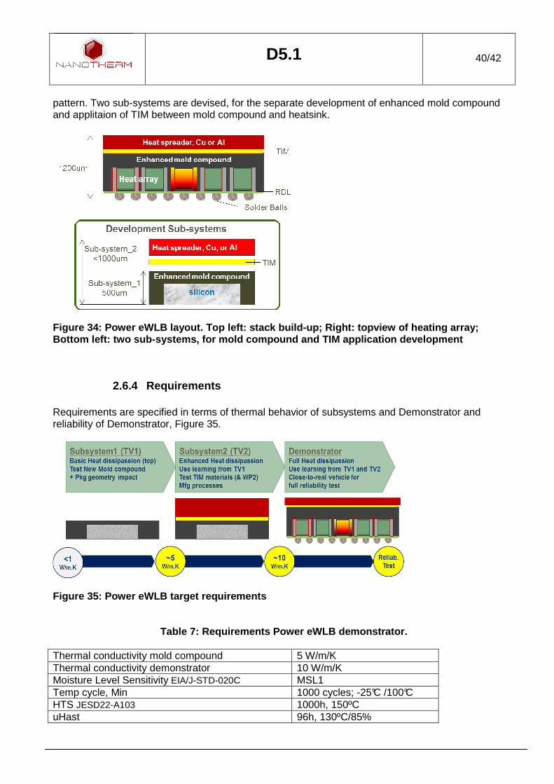
D5.1
40/42
pattern. Two sub-systems are devised, for the separate development of enhanced mold compound and applitaion of TIM between mold compound and heatsink.
Figure 34: Power eWLB layout. Top left: stack build -up; Right: topview of heating array; Bottom left: two sub-systems, for mold compound and TIM application development
2.6.4 Requirements
Requirements are specified in terms of thermal behavior of subsystems and Demonstrator and reliability of Demonstrator, Figure 35.
Figure 35: Power eWLB target requirements
Table 7: Requirements Power eWLB demonstrator.
Thermal conductivity mold compound 5 W/m/K Thermal conductivity demonstrator 10 W/m/K Moisture Level Sensitivity EIA/J-STD-020C MSL1 Temp cycle, Min 1000 cycles; -25°C /100°C HTS JESD22-A103 1000h, 150ºC uHast 96h, 130ºC/85%

D5.1
41/42
Environment, THB JESD22-A101 1000h 85°C/85%RH
2.6.5 Pre-Selected Materials and Technologies
For the mold compound developed and evaluated in subsystem_1, the starting point are the mold compounds types available from the qualified supplier for Nanium S.A. (Nagase), either the current type being used in production and other being developed at the manufacturer for enhanced thermal conductivity. Upon the selection of the best initial mold compound, Exfoliated Graphene developed and produced by Chalmers University will be added. For the TIM, interfacing the mold compound to the heatsink, Silver nano-flakes epoxies from AMEPOX and/or Sinter Adhesive from HERAEUS, both being developed in Nanotherm project.
2.6.6 Initial Results, Sub-system 1
The first subsystem aimed the selection of mold compound (MC), the evaluation of graphene-added MC, and the evaluation of the impact of geometry in the thermal behavior of the subsystem. A MC of 3.1W/m/K, from Nagase, with alumina fillers, was selected as candidate for the addition of graphene. 0.2% wt of graphene was added during the manufacturing of the new MC (MC2+) and Table 8 summarizes the results. No significant thermal improvement was achieved and viscosity increased 3x, bringing the MC to the limit of manufacturability. Table 8: Results of addition of 0.2%graphene to MC2 .
Units for subsystem 1 were produced, with several geometry arrangements and with the different MC’s, with and w/o graphene. Table 9 summarizes the thermal resistance values (bottom-top). Again no thermal conductivity advantages were observed by adding graphene and direct comparison (under same package geometries) even show slightly worse results whem adding graphene, likely due to the surface topology resulted from the graphene-added MC. It is also observed that MC choice has larger impact on thermal conductivity than geometry factors.

D5.1
42/42
Table 9: Thermal resistance results of the several variants of subsystem1.
Summarizing results:
• MC selection w/ larger impact than geometry on thermal performance of eWLB
o RthMC1 ≅ 2xRthMC2
o RthNoSi ≅ 2xRthFull_Si
• Selected MC2, with 3.1 W/m/K, with alumina fillers for subsystem 2
• MC2+ 0.2% graphene:
o High impact on viscosity, processability of compression molding at the limit
o Low impact on thermal performance;
o Investigation of graphene-added MC will continue in parallel, for enhanced functionality, but
subsystem2 will proceed with no graphene added MC