innolux g080y1-t01 tft-display distributed by data … · tcon (timing controller) ... 2 vgl i gate...
TRANSCRIPT
G080Y1-T01
8” TFT - WVGA - TTL
Version: 2.3Date: 18.01.2011
Note: This specification is subject to change without prior notice
SPECIFICATION
w w w . d a t a - m o d u l . c o m
PRODUCT SPECIFICATION
Version 2.3 18 January 2011 1 / 28
The copyright belongs to CHIMEI InnoLux. Any unauthorized use is prohibited.
Customer: APPROVED BY SIGNATURE Name / Title Note Please return 1 copy for your confirmation with your signature and comments.
Doc. Number :
□ Tentative Specification □ Preliminary Specification
■ Approval Specification
MODEL NO.: G080Y1
SUFFIX: T01
核准時間 部門 審核 角色 投票
2011-01-24 18:57:55
APPL 產品管理處
yuhsiang.chang (張喻翔)
Director Accept
Data Modul AG - www.data-modul.com
PRODUCT SPECIFICATION
Version 2.3 18 January 2011 2 / 28
The copyright belongs to CHIMEI InnoLux. Any unauthorized use is prohibited.
- CONTENTS - REVISION HISTORY ------------------------------------------------------- 3 1. GENERAL DESCRIPTION ------------------------------------------------------- 4 1.1 OVERVIEW 1.2 FEATURES 1.3 APPLICATION 1.4 GENERAL SPECIFICATIONS 1.5 MECHANICAL SPECIFICATIONS 2. ABSOLUTE MAXIMUM RATINGS ------------------------------------------------------- 6 2.1 ABSOLUTE RATINGS OF ENVIRONMENT 2.2 ELECTRICAL ABSOLUTE RATINGS 2.2.1 TFT LCD MODULE 2.2.2 BACKLIGHT UNIT 3. ELECTRICAL CHARACTERISTICS ------------------------------------------------------- 8
3.1 RECOMMENDED OPERATIN CONDITION 3.2 CURRENT CONSUMPTION 3.3 BACKLIGHT UNIT
4. BLOCK DIAGRAM ------------------------------------------------------- 10
4.1 TFT LCD MODULE 4.2 BACKLIGHT UNIT
5. INPUT TERMINAL PIN ASSIGNMENT ------------------------------------------------------- 11
5.1 FPC I/O PIN ASSIGNMENT 5.2 BACKLIGHT DRIVING SECTION
5.3 SCANNING DIRECTION 5.4 COLOR DATA INPUT ASSIGNMENT 6. INTERFACE TIMING ------------------------------------------------------- 16 6.1 AC ELECTRICAL CHARACTERISTICS 6.2 POWER ON/OFF SEQUENCE 7. OPTICAL CHARACTERISTICS ------------------------------------------------------- 19 7.1 TEST CONDITIONS 7.2 OPTICAL SPECIFICATIONS 8. RELIABLITY TEST ------------------------------------------------------- 22 9. PACKAGING ------------------------------------------------------- 23 10. DEFINTION OF LABELS ------------------------------------------------------- 25 11. PRECATIONS -------------------------------------------------------- 26
11.1 ASSEMBLY AND HANDLING PRECAUTIONS
11.2 SAFETY PRECAUTIONS
12. MECHANICAL DRAWING -------------------------------------------------------- 27
Data Modul AG - www.data-modul.com
PRODUCT SPECIFICATION
Version 2.3 18 January 2011 3 / 28
The copyright belongs to CHIMEI InnoLux. Any unauthorized use is prohibited.
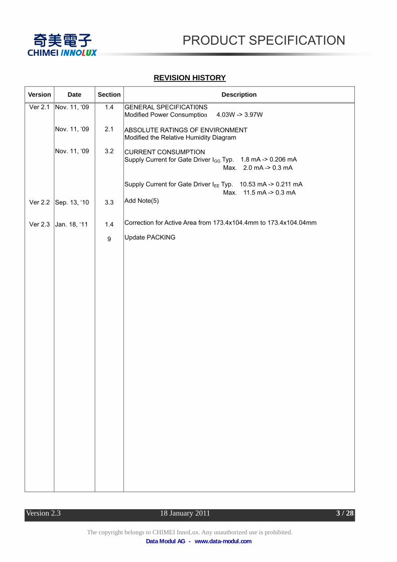
REVISION HISTORY
Version Date Section Description
Ver 2.1
Ver 2.2
Ver 2.3
Nov. 11, ‘09 Nov. 11, ‘09 Nov. 11, ‘09 Sep. 13, ‘10 Jan. 18, ‘11
1.4
2.1
3.2
3.3
1.4 9
GENERAL SPECIFICATI0NS Modified Power Consumption: 4.03W -> 3.97W ABSOLUTE RATINGS OF ENVIRONMENT Modified the Relative Humidity Diagram CURRENT CONSUMPTION Supply Current for Gate Driver IGG Typ.:1.8 mA -> 0.206 mA Max.:2.0 mA -> 0.3 mA
Supply Current for Gate Driver IEE Typ.:10.53 mA -> 0.211 mA Max.:11.5 mA -> 0.3 mA Add Note(5) Correction for Active Area from 173.4x104.4mm to 173.4x104.04mm Update PACKING
Data Modul AG - www.data-modul.com
PRODUCT SPECIFICATION
Version 2.3 18 January 2011 4 / 28
The copyright belongs to CHIMEI InnoLux. Any unauthorized use is prohibited.
1. GENERAL DESCRIPTION 1.1 OVERVIEW
G080Y1-T01 is a 8inch TFT Liquid Crystal Display module with a LED backlight unit and
a-60-pin-and-1ch-TTL interface. TCON (timing controller) is included in driver IC. This module supports
800 (R.G.B )x 480 WVGA mode which main application is the automotive display and industrial field.
1.2 FEATURES - Wide viewing angle.
- Fast response time
- High Color Gamut (NTSC:72%)
- Wide operating temperature
- Reversible - scan function
- 6/8 bit convertible
1.3 APPLICATION - Automotive Display
- Industry Application
1.4 GENERAL SPECIFICATI0NS Item Specification Unit Note
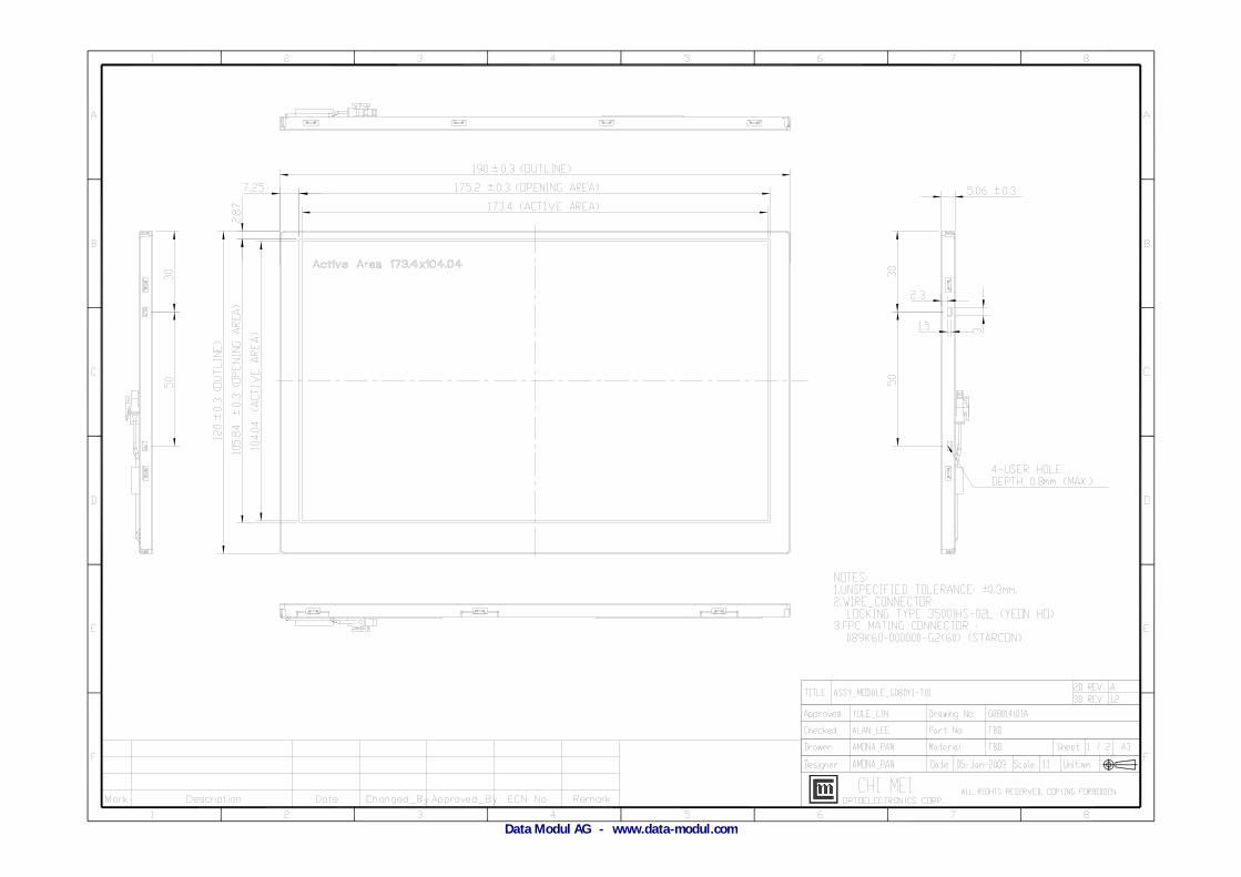
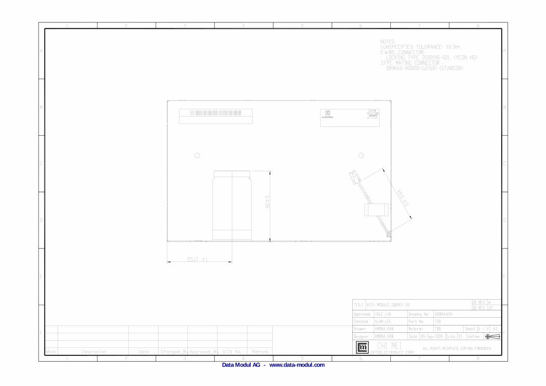
Diagonal Size 8 inch Active Area 173.4x104.04 mm Bezel Opening Area 175.2x105.84 mm (1)
Driver Element a-si TFT active matrix - - Pixel Number 800 x R.G.B. x 480 pixel - Pixel Pitch 0.2168 x 0.2168 mm - Pixel Arrangement RGB vertical stripe - (3) Display Colors 262k or 16.2M color - Display Mode Normal White - - Surface Treatment Anti-glare, Hard Coating ( 3H ) - - Weight 172 g - Power consumption 3.97 W (2)
Note (1) Please refer to the attached drawings for more information of front and back outline dimensions.
Note (2) Power consumption doesn’t include LED converter.
Data Modul AG - www.data-modul.com
PRODUCT SPECIFICATION
Version 2.3 18 January 2011 5 / 28
The copyright belongs to CHIMEI InnoLux. Any unauthorized use is prohibited.
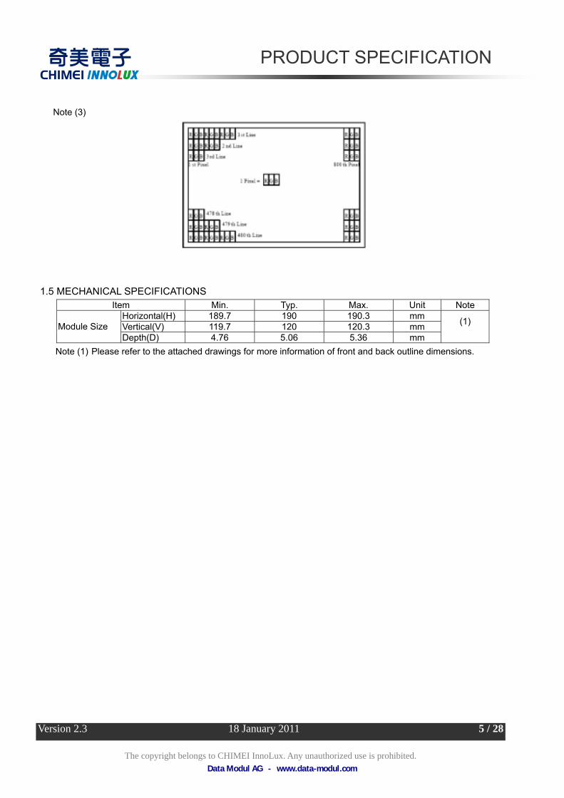
Note (3)
1.5 MECHANICAL SPECIFICATIONS
Item Min. Typ. Max. Unit Note Horizontal(H) 189.7 190 190.3 mm Vertical(V) 119.7 120 120.3 mm Module Size Depth(D) 4.76 5.06 5.36 mm
(1)
Note (1) Please refer to the attached drawings for more information of front and back outline dimensions.
Data Modul AG - www.data-modul.com
PRODUCT SPECIFICATION
Version 2.3 18 January 2011 6 / 28
The copyright belongs to CHIMEI InnoLux. Any unauthorized use is prohibited.
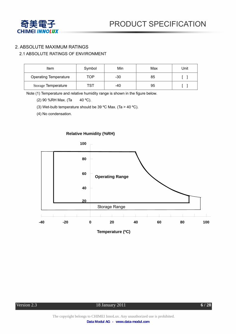
2. ABSOLUTE MAXIMUM RATINGS 2.1 ABSOLUTE RATINGS OF ENVIRONMENT
Item Symbol Min Max Unit
Operating Temperature TOP -30℃ 85℃ [℃]
Storage Temperature TST -40℃ 95℃ [℃]
Note (1) Temperature and relative humidity range is shown in the figure below.
(2) 90 %RH Max. (Ta ≦ 40 ºC).
(3) Wet-bulb temperature should be 39 ºC Max. (Ta > 40 ºC).
(4) No condensation.
-40
Relative Humidity (%RH)
Operating Range
Temperature (ºC)
100
80 60 -20 40 0 20
80
40
60
20 Storage Range
100
Data Modul AG - www.data-modul.com
PRODUCT SPECIFICATION
Version 2.3 18 January 2011 7 / 28
The copyright belongs to CHIMEI InnoLux. Any unauthorized use is prohibited.
2.2 ELECTRICAL ABSOLUTE RATINGS 2.2.1 TFT LCD MODULE Ta = 25 ± 2 ºC
Value Parameter Symbol Min. Max. Unit Note
VCC -0.3 6 V - AVDD 6.5 13.5 V - VGH 7 VGL+40 V
Power Supply Voltage
VGL -20 -5 V - Digital Input Voltage VI 0.3 VCC+0.3 V (1)
V1~V5 0.4AVDD AVDD-0.3 V - Gamma Supply Voltage
V6~V10 0.3 0.6AVDD V -
Note (1) VI means all input logic signal.
2.2.2 BACKLIGHT UNIT Ta = 25 ± 2 ºC Value Unit Note Item Symbol Min. Max.
LED Light Bar Power Supply Voltage VL -30 35 V (1)
LED Light Bar Power Supply Current IL 130 mA (1)
Note (1) Permanent damage to the device may occur if maximum or minimum values are exceeded.
Function operation should be restricted to the conditions described under Normal Operating
Conditions.
Data Modul AG - www.data-modul.com
PRODUCT SPECIFICATION
Version 2.3 18 January 2011 8 / 28
The copyright belongs to CHIMEI InnoLux. Any unauthorized use is prohibited.
3. ELECTRICAL CHARACTERISTICS 3.1 RECOMMENDED OPERATION CONDITION (GND = AVSS = 0V) Ta = 25 ± 2 ºC
Value Parameter Symbol Min. Typ. Max. Unit Note
VCC 3.0 3.3 3.6 V AVDD 11.5 12 12.5 V VGH 17 18 19 V
Power Supply Voltage
VGL -8 -7 -6 V V1~V5 0.4AVDD AVDD-0.3 V V6~V10 0.3 0.6AVDD V Input Signal Voltage VCOM 4.3 V
High Level VIH 0.7VCC VCC V Digital Input Voltage
Low Level VIL 0 0.3VCC V
3.2 CURRENT CONSUMPTION (GND = AVSS =0V) Ta = 25 ± 2 ºC Value Parameter Symbol Min. Typ. Max. Unit Note
Supply Current for Source/Gate Driver (Digital) ICC - 22.8 25 mA (1)
Supply Current for Source Driver (Analog) IDD - 36.5 38 mA (1)
Supply Current for Gate Driver (High Level) IGG - 0.206 0.3 mA (1)
Supply Current for Gate Driver (Low Level) IEE - 0.211 0.3 mA (1)
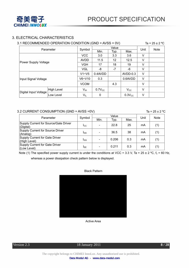
Note (1) The specified power supply current is under the conditions at VCC = 3.3 V, Ta = 25 ± 2 ºC, fv = 60 Hz,
whereas a power dissipation check pattern below is displayed.
Active Area
Black Pattern
Data Modul AG - www.data-modul.com
PRODUCT SPECIFICATION
Version 2.3 18 January 2011 9 / 28
The copyright belongs to CHIMEI InnoLux. Any unauthorized use is prohibited.
3.3 BACKLIGHT UNIT Ta = 25 ± 2 ºC Value
Parameter Symbol Min. Typ. Max. Unit Note
LED Light Bar Power Supply Voltage VL 28.8 31.5 V TBD
LED Light Bar Power Supply Current IL - 120 130 mA
Power Consumption PL - 3.45 - W
(1),(2) (Duty 100%)
(3), (Duty 100%)LED Life Time LBL 30000 - hr
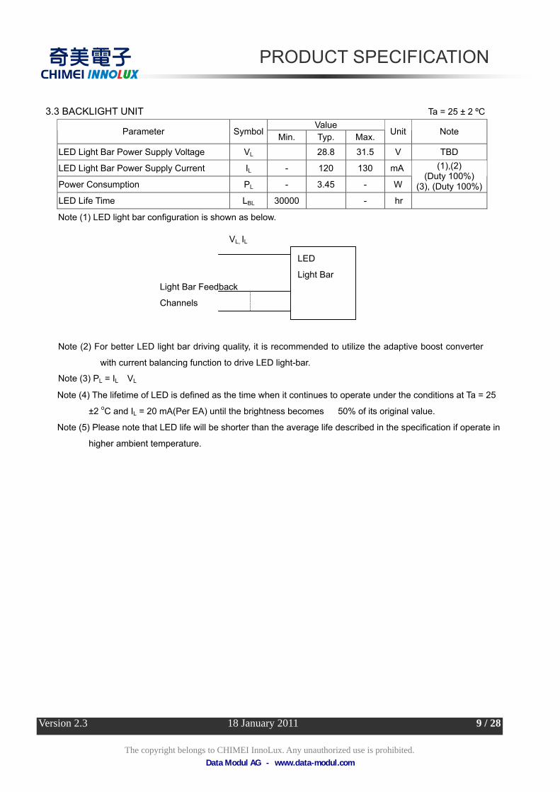
Note (1) LED light bar configuration is shown as below.
Note (2) For better LED light bar driving quality, it is recommended to utilize the adaptive boost converter
with current balancing function to drive LED light-bar.
Note (3) PL = IL ×VL
Note (4) The lifetime of LED is defined as the time when it continues to operate under the conditions at Ta = 25
±2 oC and IL = 20 mA(Per EA) until the brightness becomes 50% of its original value.≦
Note (5) Please note that LED life will be shorter than the average life described in the specification if operate in
higher ambient temperature.
LED
Light Bar
VL, IL
Light Bar Feedback
Channels
Data Modul AG - www.data-modul.com
PRODUCT SPECIFICATION
Version 2.3 18 January 2011 10 / 28
The copyright belongs to CHIMEI InnoLux. Any unauthorized use is prohibited.
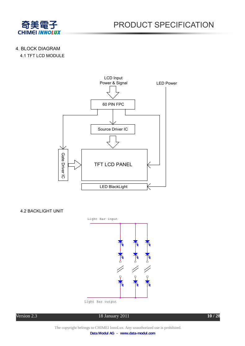
4. BLOCK DIAGRAM 4.1 TFT LCD MODULE
LCD InputPower & Signal
Source Driver IC
60 PIN FPC
Gate D
river IC
TFT LCD PANEL
LED Power
LED BlackLight
4.2 BACKLIGHT UNIT
Light Bar output
Light Bar input
Data Modul AG - www.data-modul.com
PRODUCT SPECIFICATION
Version 2.3 18 January 2011 11 / 28
The copyright belongs to CHIMEI InnoLux. Any unauthorized use is prohibited.
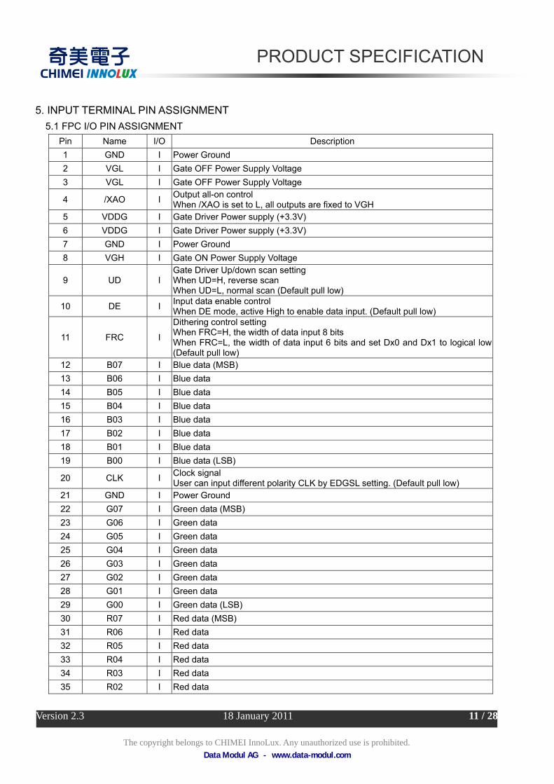
5. INPUT TERMINAL PIN ASSIGNMENT 5.1 FPC I/O PIN ASSIGNMENT
Pin Name I/O Description 1 GND I Power Ground 2 VGL I Gate OFF Power Supply Voltage 3 VGL I Gate OFF Power Supply Voltage
4 /XAO I Output all-on control When /XAO is set to L, all outputs are fixed to VGH
5 VDDG I Gate Driver Power supply (+3.3V) 6 VDDG I Gate Driver Power supply (+3.3V) 7 GND I Power Ground 8 VGH I Gate ON Power Supply Voltage
9 UD I Gate Driver Up/down scan setting When UD=H, reverse scan When UD=L, normal scan (Default pull low)
10 DE I Input data enable control When DE mode, active High to enable data input. (Default pull low)
11 FRC I Dithering control setting When FRC=H, the width of data input 8 bits When FRC=L, the width of data input 6 bits and set Dx0 and Dx1 to logical low (Default pull low)
12 B07 I Blue data (MSB) 13 B06 I Blue data 14 B05 I Blue data 15 B04 I Blue data 16 B03 I Blue data 17 B02 I Blue data 18 B01 I Blue data 19 B00 I Blue data (LSB) 20 CLK I Clock signal
User can input different polarity CLK by EDGSL setting. (Default pull low) 21 GND I Power Ground 22 G07 I Green data (MSB) 23 G06 I Green data 24 G05 I Green data 25 G04 I Green data 26 G03 I Green data 27 G02 I Green data 28 G01 I Green data 29 G00 I Green data (LSB) 30 R07 I Red data (MSB) 31 R06 I Red data 32 R05 I Red data 33 R04 I Red data 34 R03 I Red data 35 R02 I Red data
Data Modul AG - www.data-modul.com
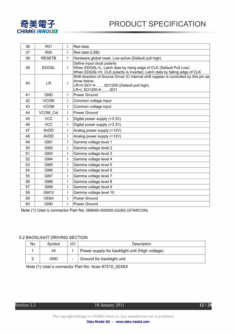
PRODUCT SPECIFICATION
Version 2.3 18 January 2011 12 / 28
The copyright belongs to CHIMEI InnoLux. Any unauthorized use is prohibited.
36 R01 I Red data 37 R00 I Red data (LSB) 38 RESETB I Hardware global reset. Low active (Default pull high)
39 EDGSL I Define input clock polarity When EDGSL=L, Latch data by rising edge of CLK (Default Pull Low) When EDGSL=H, CLK polarity is inverted, Latch data by falling edge of CLK
40 LR I Shift direction of Source Driver IC internal shift register is controlled by this pin as show below: LR=H SO1 ……SO1200 (Default pull high) LR=L SO1200 …….SO1
41 GND I Power Ground 42 VCOM I Common voltage input 43 VCOM I Common voltage input 44 VCOM_Cst I Power Ground 45 VCC I Digital power supply (+3.3V) 46 VCC I Digital power supply (+3.3V) 47 AVDD I Analog power supply (+12V) 48 AVDD I Analog power supply (+12V) 49 GM1 I Gamma voltage level 1 50 GM2 I Gamma voltage level 2 51 GM3 I Gamma voltage level 3 52 GM4 I Gamma voltage level 4 53 GM5 I Gamma voltage level 5 54 GM6 I Gamma voltage level 6 55 GM7 I Gamma voltage level 7 56 GM8 I Gamma voltage level 8 57 GM9 I Gamma voltage level 9 58 GM10 I Gamma voltage level 10 59 VSSA I Power Ground 60 GND I Power Ground
Note (1) User’s connector Part No: 089K60-000000-G2(60) (STARCON)
5.2 BACKLIGHT DRIVING SECTION
No Symbol I/O Description
1 Hi I Power supply for backlight unit (High voltage)
2 GND - Ground for backlight unit
Note (1) User’s connector Part No: Aces 87210_02X6X
Data Modul AG - www.data-modul.com
PRODUCT SPECIFICATION
Version 2.3 18 January 2011 13 / 28
The copyright belongs to CHIMEI InnoLux. Any unauthorized use is prohibited.
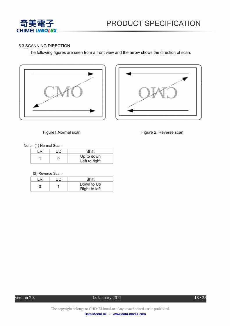
5.3 SCANNING DIRECTION The following figures are seen from a front view and the arrow shows the direction of scan.
Figure1.Normal scan Figure 2. Reverse scan
Note : (1) Normal Scan LR UD Shift
1 0 Up to down Left to right
(2) Reverse Scan LR UD Shift
0 1 Down to Up Right to left
Data Modul AG - www.data-modul.com
PRODUCT SPECIFICATION
Version 2.3 18 January 2011 14 / 28
The copyright belongs to CHIMEI InnoLux. Any unauthorized use is prohibited.
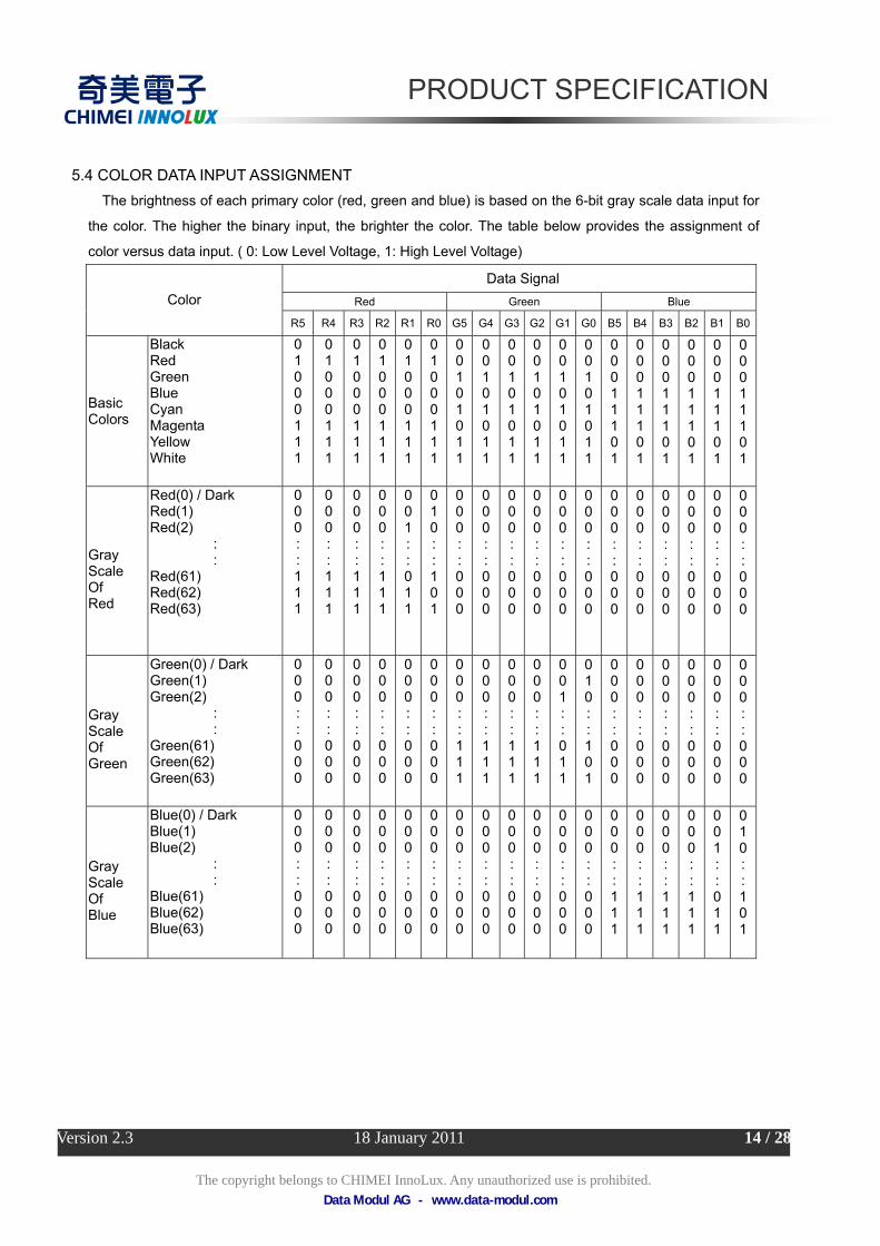
5.4 COLOR DATA INPUT ASSIGNMENT The brightness of each primary color (red, green and blue) is based on the 6-bit gray scale data input for
the color. The higher the binary input, the brighter the color. The table below provides the assignment of
color versus data input. ( 0: Low Level Voltage, 1: High Level Voltage)
Data Signal Red Green Blue Color
R5 R4 R3 R2 R1 R0 G5 G4 G3 G2 G1 G0 B5 B4 B3 B2 B1 B0
Basic Colors
Black Red Green Blue Cyan Magenta Yellow White
0 1 0 0 0 1 1 1
0 1 0 0 0 1 1 1
01000111
01000111
01000111
01000111
00101011
00101011
00101011
00101011
00101011
00101011
0 0 0 1 1 1 0 1
0 0 0 1 1 1 0 1
0 0 0 1 1 1 0 1
0 0 0 1 1 1 0 1
00011101
00011101
Gray Scale Of Red
Red(0) / Dark Red(1) Red(2)
: :
Red(61) Red(62) Red(63)
0 0 0 : : 1 1 1
0 0 0 : : 1 1 1
000::111
000::111
001::011
010::101
000::000
000::000
000::000
000::000
000::000
000::000
0 0 0 : : 0 0 0
0 0 0 : : 0 0 0
0 0 0 : : 0 0 0
0 0 0 : : 0 0 0
000::000
000::000
Gray Scale Of Green
Green(0) / Dark Green(1) Green(2)
: :
Green(61) Green(62) Green(63)
0 0 0 : : 0 0 0
0 0 0 : : 0 0 0
000::000
000::000
000::000
000::000
000::111
000::111
000::111
000::111
001::011
010::101
0 0 0 : : 0 0 0
0 0 0 : : 0 0 0
0 0 0 : : 0 0 0
0 0 0 : : 0 0 0
000::000
000::000
Gray Scale Of Blue
Blue(0) / Dark Blue(1) Blue(2)
: :
Blue(61) Blue(62) Blue(63)
0 0 0 : : 0 0 0
0 0 0 : : 0 0 0
000::000
000::000
000::000
000::000
000::000
000::000
000::000
000::000
000::000
000::000
0 0 0 : : 1 1 1
0 0 0 : : 1 1 1
0 0 0 : : 1 1 1
0 0 0 : : 1 1 1
001::011
010::101
Data Modul AG - www.data-modul.com
PRODUCT SPECIFICATION
Version 2.3 18 January 2011 15 / 28
The copyright belongs to CHIMEI InnoLux. Any unauthorized use is prohibited.
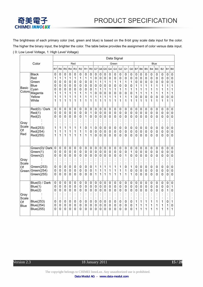
The brightness of each primary color (red, green and blue) is based on the 8-bit gray scale data input for the color.
The higher the binary input, the brighter the color. The table below provides the assignment of color versus data input.
( 0: Low Level Voltage, 1: High Level Voltage)
Data Signal Red Green Blue Color
R7 R6 R5 R4 R3 R2 R1 R0 G7 G6 G5 G4 G3 G2 G1 G0 B7 B6 B5 B4 B3 B2 B1 B0
Basic Colors
Black Red Green Blue Cyan Magenta Yellow White
0 1 0 0 0 1 1 1
0 1 0 0 0 1 1 1
0 1 0 0 0 1 1 1
0 1 0 0 0 1 1 1
0 1 0 0 0 1 1 1
01000111
01000111
01000111
00101011
00101011
00101011
00101011
00101011
00101011
00101011
00101011
00011101
0 0 0 1 1 1 0 1
0 0 0 1 1 1 0 1
0 0 0 1 1 1 0 1
0 0 0 1 1 1 0 1
00011101
00011101
00011101
Gray Scale Of Red
Red(0) / Dark Red(1) Red(2)
: :
Red(253) Red(254) Red(255)
0 0 0 : : 1 1 1
0 0 0 : : 1 1 1
0 0 0 : : 1 1 1
0 0 0 : : 1 1 1
0 0 0 : : 1 1 1
000::111
001::011
010::101
000::000
000::000
000::000
000::000
000::000
000::000
000::000
000::000
000::000
0 0 0 : : 0 0 0
0 0 0 : : 0 0 0
0 0 0 : : 0 0 0
0 0 0 : : 0 0 0
000::000
000::000
000::000
Gray Scale Of Green
Green(0)/ Dark Green(1) Green(2)
: :
Green(253) Green(254) Green(255)
0 0 0 : : 0 0 0
0 0 0 : : 0 0 0
0 0 0 : : 0 0 0
0 0 0 : : 0 0 0
0 0 0 : : 0 0 0
000::000
000::000
000::000
000::111
000::111
000::111
000::111
000::111
000::111
001::011
010::101
000::000
0 0 0 : : 0 0 0
0 0 0 : : 0 0 0
0 0 0 : : 0 0 0
0 0 0 : : 0 0 0
000::000
000::000
000::000
Gray Scale Of Blue
Blue(0) / Dark Blue(1) Blue(2)
: :
Blue(253) Blue(254) Blue(255)
0 0 0 : : 0 0 0
0 0 0 : : 0 0 0
0 0 0 : : 0 0 0
0 0 0 : : 0 0 0
0 0 0 : : 0 0 0
000::000
000::000
000::000
000::000
000::000
000::000
000::000
000::000
000::000
000::000
000::000
000::111
0 0 0 : : 1 1 1
0 0 0 : : 1 1 1
0 0 0 : : 1 1 1
0 0 0 : : 1 1 1
000::111
001::011
010::101
Data Modul AG - www.data-modul.com
PRODUCT SPECIFICATION
Version 2.3 18 January 2011 16 / 28
The copyright belongs to CHIMEI InnoLux. Any unauthorized use is prohibited.
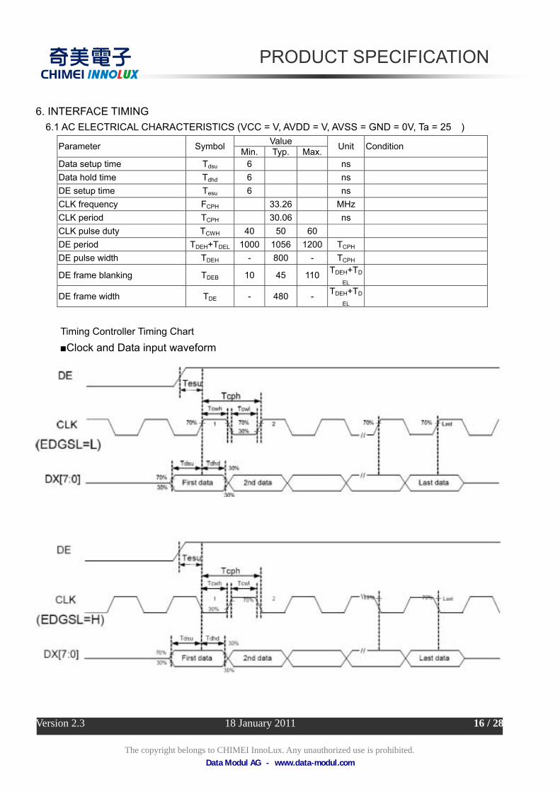
6. INTERFACE TIMING 6.1 AC ELECTRICAL CHARACTERISTICS (VCC = V, AVDD = V, AVSS = GND = 0V, Ta = 25℃)
Value Parameter Symbol Min. Typ. Max. Unit Condition
Data setup time Tdsu 6 ns Data hold time Tdhd 6 ns DE setup time Tesu 6 ns CLK frequency FCPH 33.26 MHz CLK period TCPH 30.06 ns CLK pulse duty TCWH 40 50 60 % DE period TDEH+TDEL 1000 1056 1200 TCPH DE pulse width TDEH - 800 - TCPH
DE frame blanking TDEB 10 45 110 TDEH+TD
EL
DE frame width TDE - 480 - TDEH+TD
EL
Timing Controller Timing Chart
■Clock and Data input waveform
Data Modul AG - www.data-modul.com
PRODUCT SPECIFICATION
Version 2.3 18 January 2011 17 / 28
The copyright belongs to CHIMEI InnoLux. Any unauthorized use is prohibited.
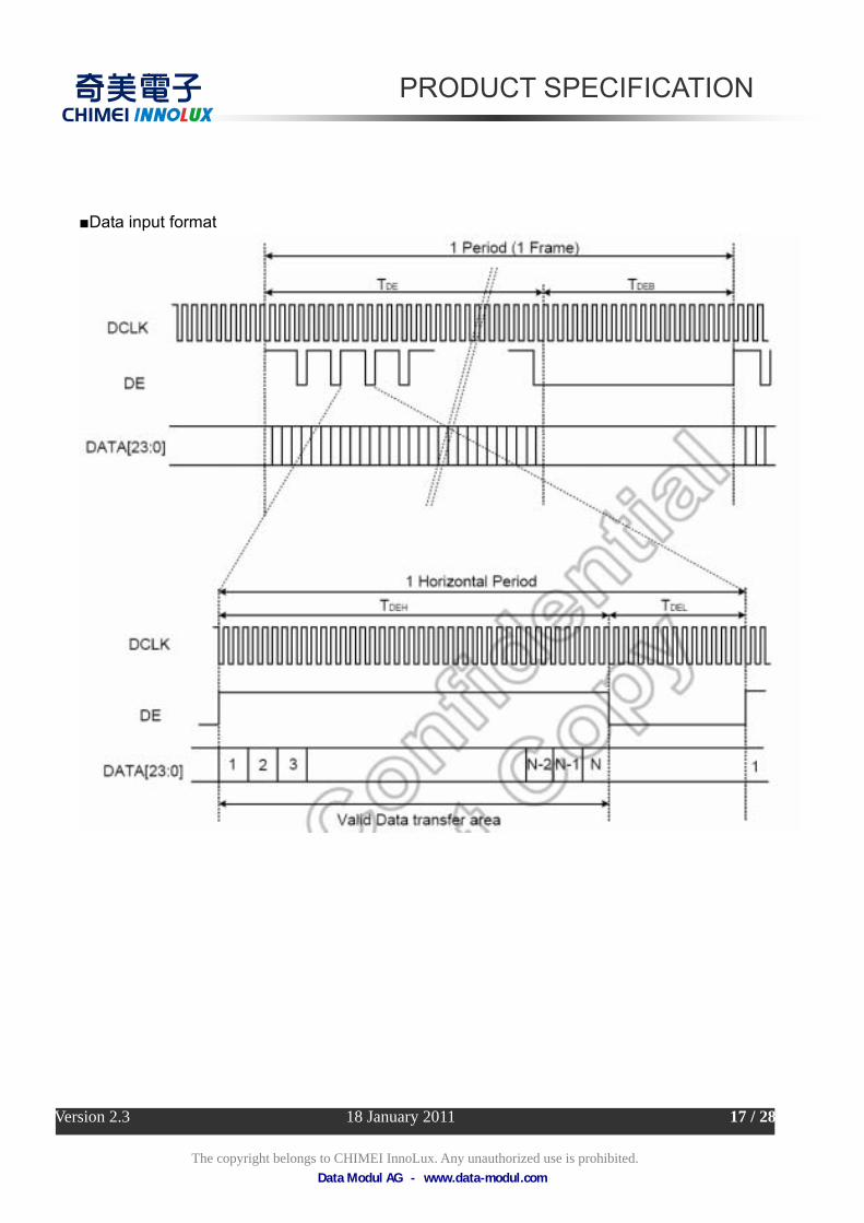
■Data input format
Data Modul AG - www.data-modul.com
PRODUCT SPECIFICATION
Version 2.3 18 January 2011 18 / 28
The copyright belongs to CHIMEI InnoLux. Any unauthorized use is prohibited.
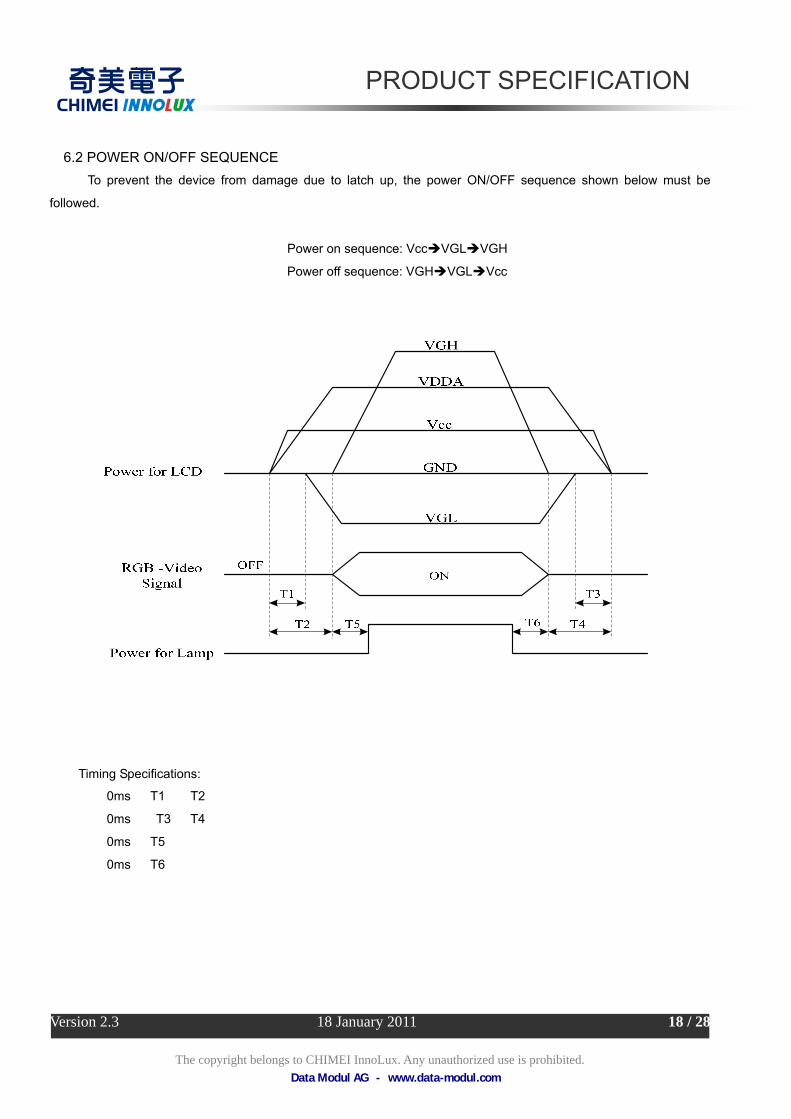
6.2 POWER ON/OFF SEQUENCE To prevent the device from damage due to latch up, the power ON/OFF sequence shown below must be
followed.
Power on sequence: Vcc VGL VGH
Power off sequence: VGH VGL Vcc
Timing Specifications:
0ms ≦ T1 < T2
0ms < T3 ≦ T4
0ms ≦ T5
0ms ≦ T6
Data Modul AG - www.data-modul.com
PRODUCT SPECIFICATION
Version 2.3 18 January 2011 19 / 28
The copyright belongs to CHIMEI InnoLux. Any unauthorized use is prohibited.
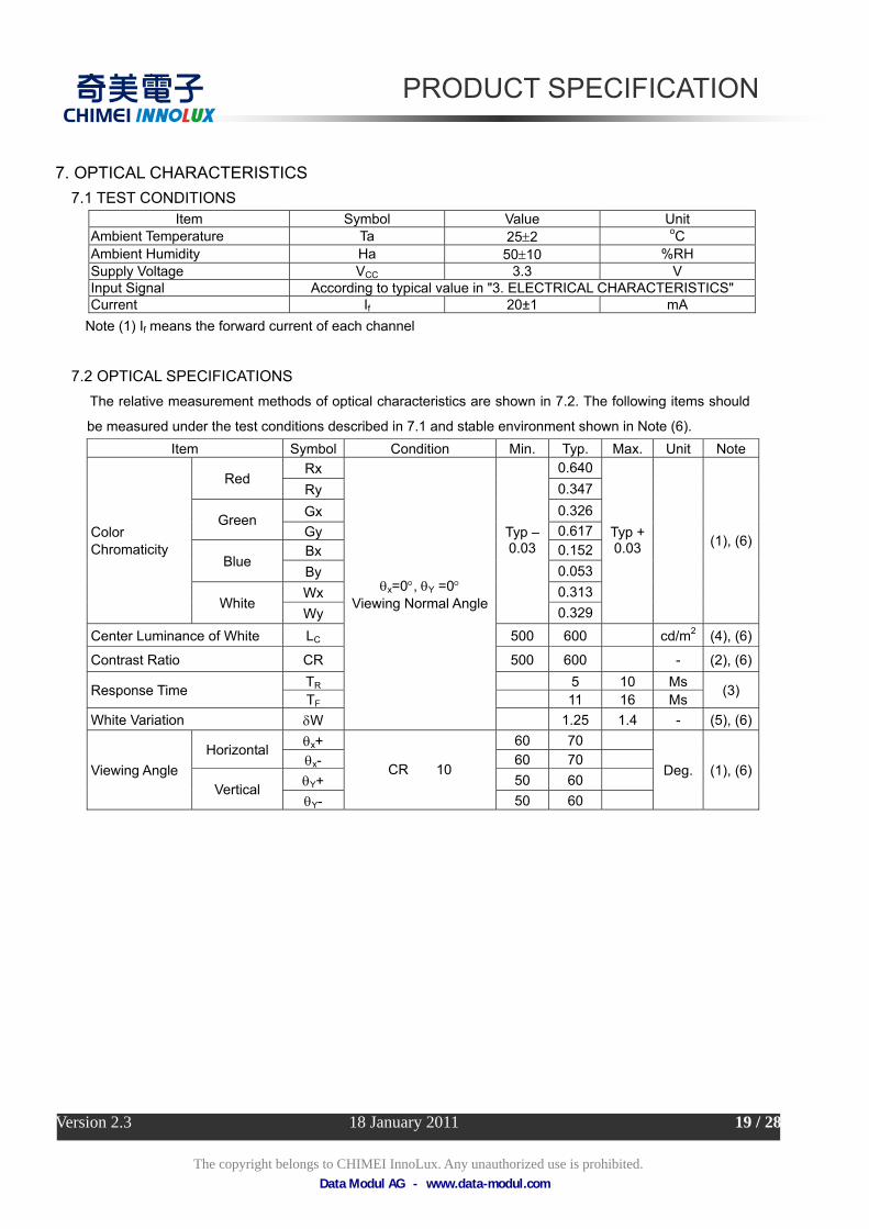
7. OPTICAL CHARACTERISTICS 7.1 TEST CONDITIONS
Item Symbol Value Unit Ambient Temperature Ta 25±2 oC Ambient Humidity Ha 50±10 %RH Supply Voltage VCC 3.3 V Input Signal According to typical value in "3. ELECTRICAL CHARACTERISTICS" Current If 20±1 mA
Note (1) If means the forward current of each channel
7.2 OPTICAL SPECIFICATIONS
The relative measurement methods of optical characteristics are shown in 7.2. The following items should
be measured under the test conditions described in 7.1 and stable environment shown in Note (6). Item Symbol Condition Min. Typ. Max. Unit Note
Rx 0.640 Red
Ry 0.347 Gx 0.326
Green Gy 0.617 Bx 0.152
Blue By 0.053 Wx 0.313
Color Chromaticity
White Wy
Typ – 0.03
0.329
Typ + 0.03 (1), (6)
Center Luminance of White LC 500 600 cd/m2 (4), (6)
Contrast Ratio CR 500 600 - (2), (6)TR 5 10 Ms Response Time TF 11 16 Ms
(3)
White Variation δW
θx=0°, θY =0° Viewing Normal Angle
1.25 1.4 - (5), (6)θx+ 60 70 Horizontal θx- 60 70 θY+ 50 60
Viewing Angle Vertical
θY-
CR ≧ 10
50 60
Deg. (1), (6)
Data Modul AG - www.data-modul.com
PRODUCT SPECIFICATION
Version 2.3 18 January 2011 20 / 28
The copyright belongs to CHIMEI InnoLux. Any unauthorized use is prohibited.
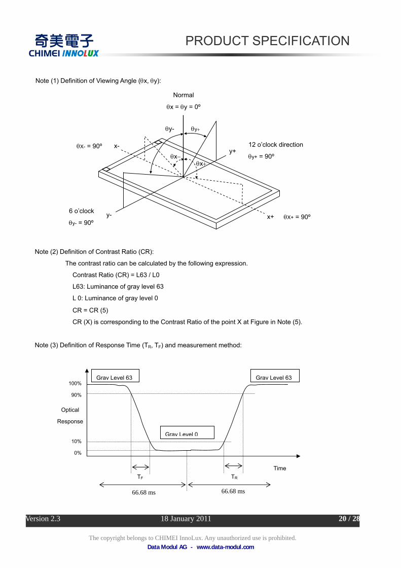
Note (1) Definition of Viewing Angle (θx, θy):
Note (2) Definition of Contrast Ratio (CR):
The contrast ratio can be calculated by the following expression.
Contrast Ratio (CR) = L63 / L0
L63: Luminance of gray level 63
L 0: Luminance of gray level 0
CR = CR (5)
CR (X) is corresponding to the Contrast Ratio of the point X at Figure in Note (5).
Note (3) Definition of Response Time (TR, TF) and measurement method:
12 o’clock direction
θy+ = 90º
6 o’clock
θy- = 90º
θx− θx+
θy- θy+
x- y+
y- x+
Normal
θx = θy = 0º
θX+ = 90º
θX- = 90º
100%
90%
10%
0%
Gray Level 63
Gray Level 0
Gray Level 63
Time TR
Optical
Response
TF
66.68 ms 66.68 ms
Data Modul AG - www.data-modul.com
PRODUCT SPECIFICATION
Version 2.3 18 January 2011 21 / 28
The copyright belongs to CHIMEI InnoLux. Any unauthorized use is prohibited.
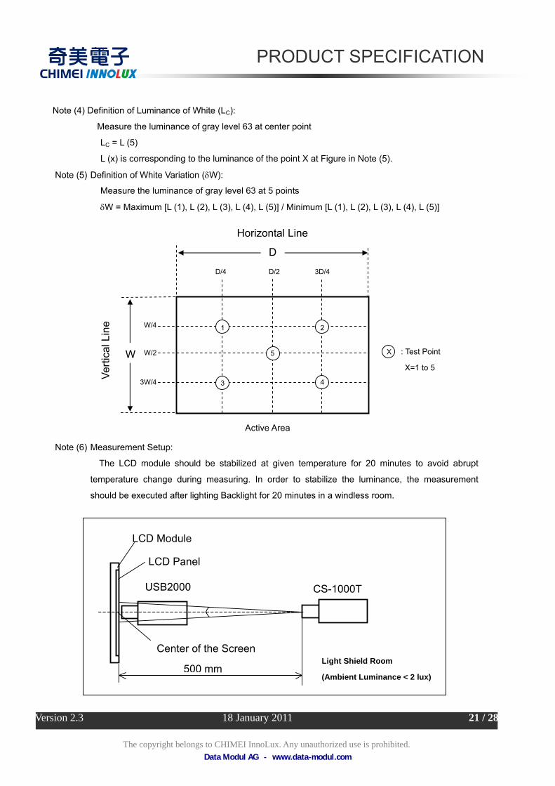
Note (4) Definition of Luminance of White (LC):
Measure the luminance of gray level 63 at center point LC = L (5)
L (x) is corresponding to the luminance of the point X at Figure in Note (5).
Note (5) Definition of White Variation (δW):
Measure the luminance of gray level 63 at 5 points
δW = Maximum [L (1), L (2), L (3), L (4), L (5)] / Minimum [L (1), L (2), L (3), L (4), L (5)]
Note (6) Measurement Setup:
The LCD module should be stabilized at given temperature for 20 minutes to avoid abrupt
temperature change during measuring. In order to stabilize the luminance, the measurement
should be executed after lighting Backlight for 20 minutes in a windless room.
D
W
Active Area
Verti
cal L
ine
Horizontal Line
: Test Point
X=1 to 5
5
1 2
3 4
D/4 D/2 3D/4
W/4
W/2
3W/4
X
CS-1000T
500 mm
LCD Module
LCD Panel
Center of the ScreenLight Shield Room
(Ambient Luminance < 2 lux)
USB2000
Data Modul AG - www.data-modul.com
PRODUCT SPECIFICATION
Version 2.3 18 January 2011 22 / 28
The copyright belongs to CHIMEI InnoLux. Any unauthorized use is prohibited.
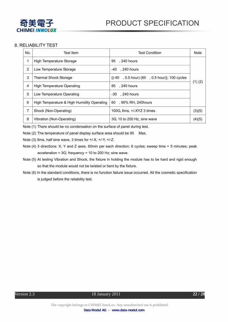
8. RELIABILITY TEST No. Test Item Test Condition Note
1 High Temperature Storage 95 , 240 hours℃
2 Low Temperature Storage -40 , 240 hours℃
3 Thermal Shock Storage {(-40℃, 0.5 hour) (85℃, 0.5 hour)}, 100 cycles
4 High Temperature Operating 85℃, 240 hours
5 Low Temperature Operating -30℃, 240 hours
6 High Temperature & High Humidity Operating 60 , 90% RH, 240hours℃
(1) (2)
7 Shock (Non-Operating) 100G, 6ms, +/-XYZ 3 times (3)(5)
8 Vibration (Non-Operating) 3G, 10 to 200 Hz, sine wave (4)(5)
Note (1) There should be no condensation on the surface of panel during test.
Note (2) The temperature of panel display surface area should be 95 Max.℃
Note (3) 6ms, half sine wave, 3 times for +/-X, +/-Y, +/-Z.
Note (4) 3 directions: X, Y and Z axes, 60min per each direction; 6 cycles; sweep time = 5 minutes; peak
acceleration = 3G; frequency = 10 to 200 Hz; sine wave.
Note (5) At testing Vibration and Shock, the fixture in holding the module has to be hard and rigid enough
so that the module would not be twisted or bent by the fixture.
Note (6) In the standard conditions, there is no function failure issue occurred. All the cosmetic specification
is judged before the reliability test.
Data Modul AG - www.data-modul.com
PRODUCT SPECIFICATION
Version 2.3 18 January 2011 23 / 28
The copyright belongs to CHIMEI InnoLux. Any unauthorized use is prohibited.
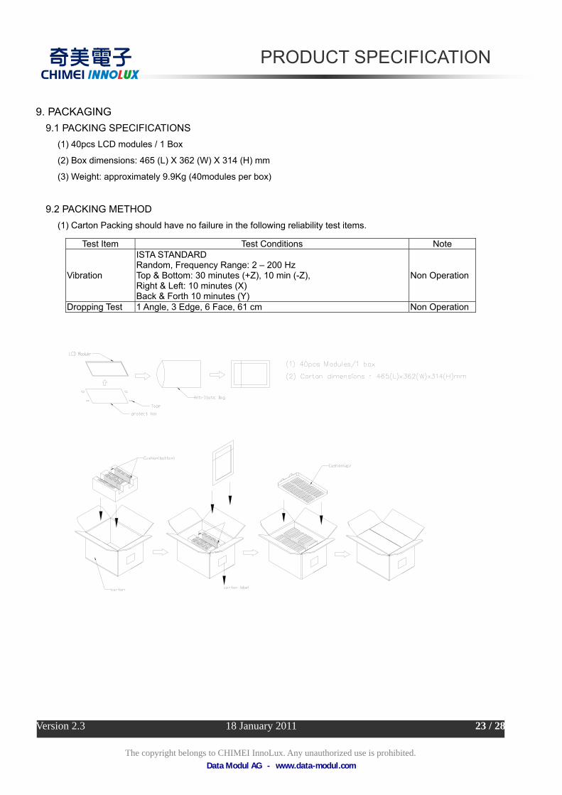
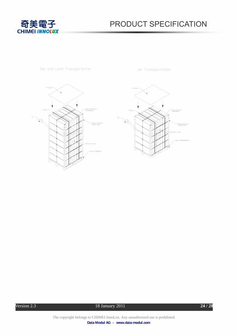
9. PACKAGING 9.1 PACKING SPECIFICATIONS
(1) 40pcs LCD modules / 1 Box
(2) Box dimensions: 465 (L) X 362 (W) X 314 (H) mm
(3) Weight: approximately 9.9Kg (40modules per box)
9.2 PACKING METHOD
(1) Carton Packing should have no failure in the following reliability test items.
Test Item Test Conditions Note
Vibration
ISTA STANDARD Random, Frequency Range: 2 – 200 Hz Top & Bottom: 30 minutes (+Z), 10 min (-Z), Right & Left: 10 minutes (X) Back & Forth 10 minutes (Y)
Non Operation
Dropping Test 1 Angle, 3 Edge, 6 Face, 61 cm Non Operation
Data Modul AG - www.data-modul.com
PRODUCT SPECIFICATION
Version 2.3 18 January 2011 24 / 28
The copyright belongs to CHIMEI InnoLux. Any unauthorized use is prohibited.
Data Modul AG - www.data-modul.com

PRODUCT SPECIFICATION
Version 2.3 18 January 2011 25 / 28
The copyright belongs to CHIMEI InnoLux. Any unauthorized use is prohibited.
E207943
10. DEFINITION OF LABELS 10.1 CMO MODULE LABEL The barcode nameplate is pasted on each module as illustration, and its definitions are as following explanation.
(a) Model Name: G080Y1 - T01
(b) Revision: Rev. XX, for example: A1, …, C1, C2 …etc.
(c) Serial ID: X X X X X X X Y M D X N N N N
Serial ID includes the information as below:
(a) Manufactured Date: Year: 1~9, for 2001~2009
Month: 1~9, A~C, for Jan. ~ Dec.
Day: 1~9, A~Y, for 1st to 31st, exclude I , O and U
(b) Revision Code: cover all the change
Serial No.: Manufacturing sequence of product
Year, Month, Date CMO Internal Use Revision
Serial No. CMO Internal Use
CMO Internal Use
CHI MEI OPTOELECTRONICS
X X X X X X X Y M D L N N N N
G080Y1 -T01 Rev.XX
RoHS
Data Modul AG - www.data-modul.com
PRODUCT SPECIFICATION
Version 2.3 18 January 2011 26 / 28
The copyright belongs to CHIMEI InnoLux. Any unauthorized use is prohibited.
11. PRECAUTIONS 11.1 ASSEMBLY AND HANDLING PRECAUTIONS
(1) Do not apply rough force such as bending or twisting to the module during assembly.
(2) To assemble or install module into user’s system can be only in clean working areas. The dust and oil
may cause electrical short or worsen the polarizer.
(3) It’s not permitted to have pressure or impulse on the module because the LCD panel and Backlight will
be damaged.
(4) Always follow the correct power sequence when LCD module is connecting and operating. This can
prevent damage to the CMOS LSI chips during latch-up.
(5) Do not pull the I/F connector in or out while the module is operating.
(6) Do not disassemble the module.
(7) Use a soft dry cloth without chemicals for cleaning, because the surface of polarizer is very soft and
easily scratched.
(8) It is dangerous that moisture come into or contacted the LCD module, because moisture may damage
LCD module when it is operating.
(9) High temperature or humidity may reduce the performance of module. Please store LCD module within
the specified storage conditions.
(10) When ambient temperature is lower than 10ºC may reduce the display quality. For example, the
response time will become slowly, and the starting voltage of CCFL will be higher than room
temperature.
(11) Do not keep same pattern in a long period of time. It may cause image sticking on LCD
11.2 SAFETY PRECAUTIONS (1) Do not disassemble the module or insert anything into the Backlight unit to prevent electrical shock.
(2) If the liquid crystal material leaks from the panel, it should be kept away from the eyes or mouth. In
case of contact with hands, skin or clothes, it has to be washed away thoroughly with soap.
(3) After the module’s end of life, it is not harmful in case of normal operation and storage.
Data Modul AG - www.data-modul.com
Data Modul AG - www.data-modul.com
Data Modul AG - www.data-modul.com

A L L T E C H N O LO G I E S . A L L CO M P E T E N C I E S . O N E S P E C I A L I S T.
w w w . d a t a - m o d u l . c o m
More information and worldwide locations can be found at
DATA MODUL AG
Landsberger Straße 322 DE-80687 Munich Phone: +49-89-56017-0
DATA MODUL WEIKERSHEIM GMBH
Lindenstraße 8 DE-97990 Weikersheim Phone: +49-7934-101-0