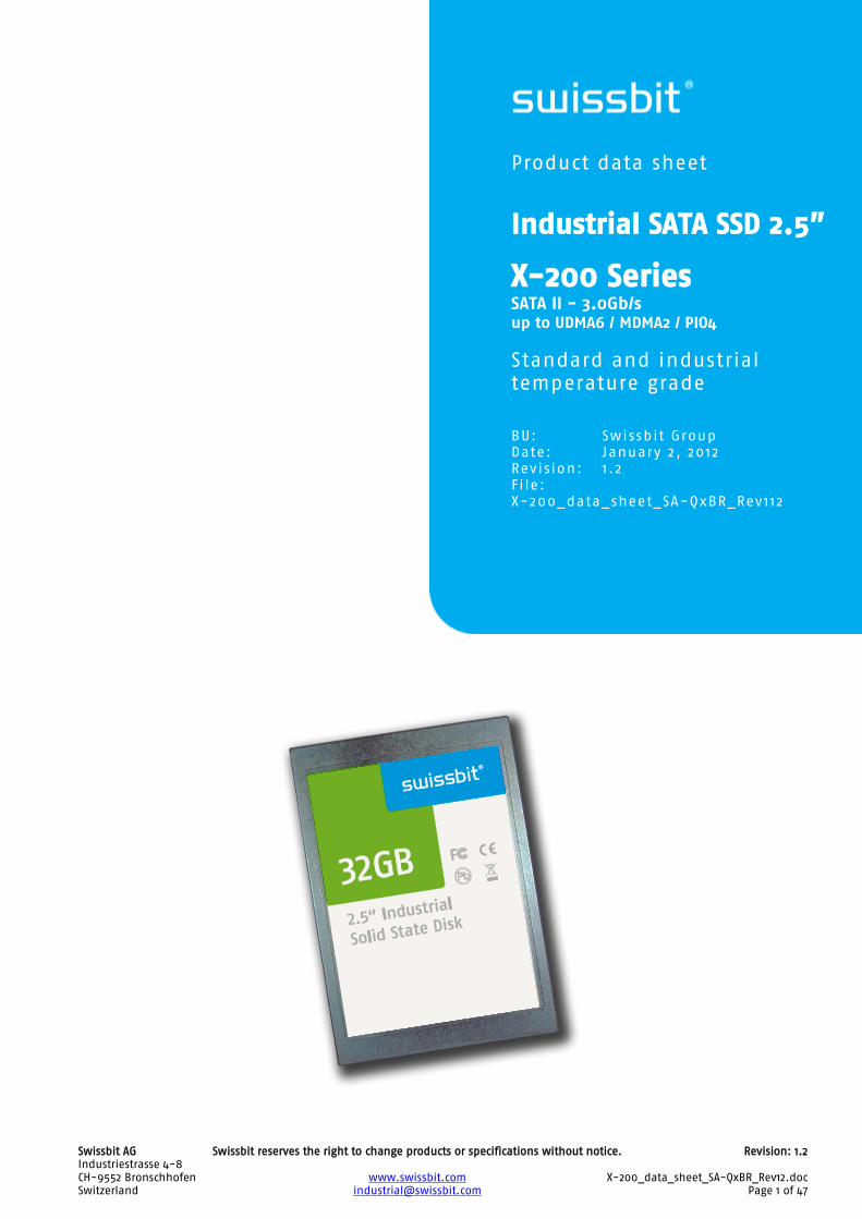
industrial sata ssd 2.5
DESCRIPTION
ÂTRANSCRIPT
Swissbit AG Swissbit reserves the right to change products or specifications without notice. Revision: 1.2 Industriestrasse 4-8
CH-9552 Bronschhofen www.swissbit.com X-200_data_sheet_SA-QxBR_Rev12.doc Switzerland [email protected] Page 1 of 47
Product data sheet
Industrial SATA SSD 2.5”
X-200 Series SATA II - 3.0Gb/s up to UDMA6 / MDMA2 / PIO4
Standard and industrial
temperature grade
BU: Swissbit Group
Date: January 2, 2012
Revision: 1 .2
Fi le :
X-200_data_sheet_SA-QxBR_Rev112
Swissbit AG Swissbit reserves the right to change products or specifications without notice. Revision: 1.2 Industriestrasse 4-8
CH-9552 Bronschhofen www.swissbit.com X-200_data_sheet_SA-QxBR_Rev12.doc Switzerland [email protected] Page 2 of 47
X-200 Series - Industrial SATA Solid State Drive 2.5”
4GByte to 64GByte
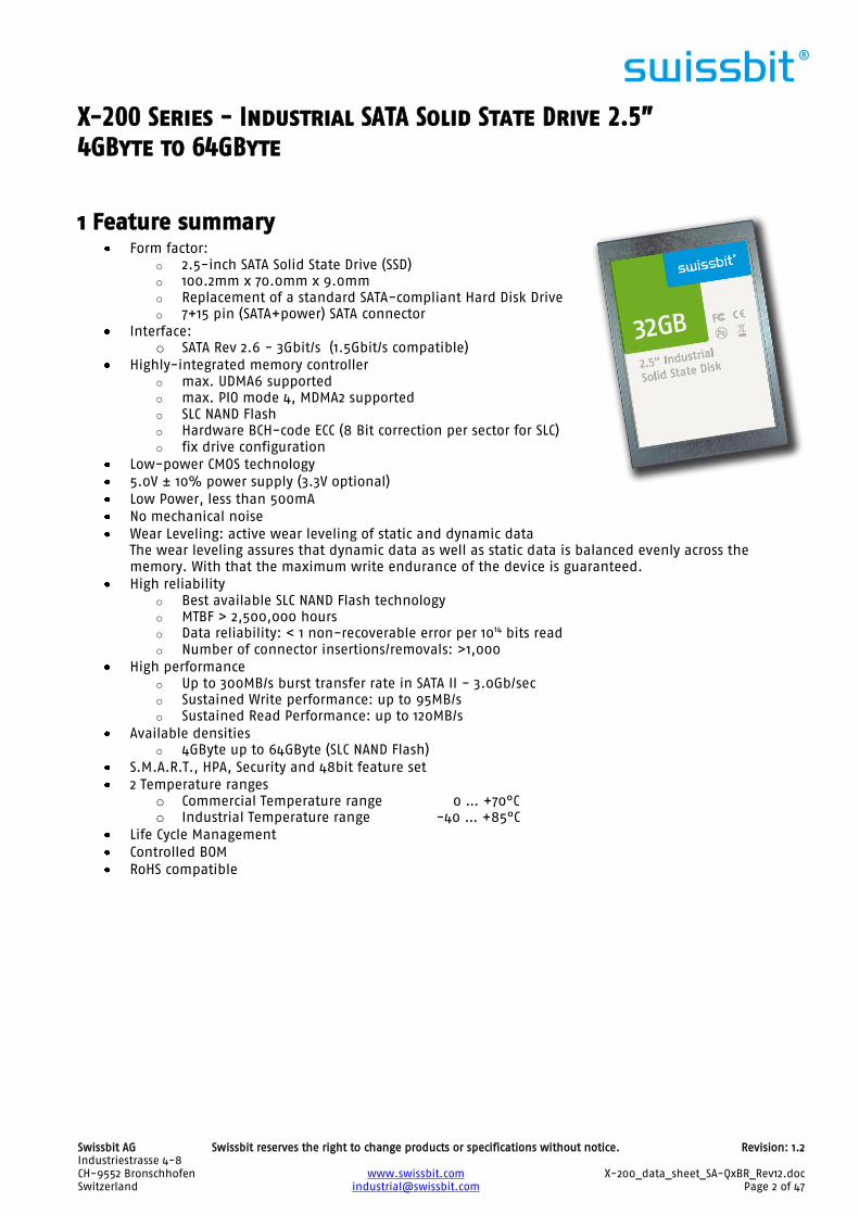
1 Feature summary Form factor:
o 2.5-inch SATA Solid State Drive (SSD)
o 100.2mm x 70.0mm x 9.0mm
o Replacement of a standard SATA-compliant Hard Disk Drive
o 7+15 pin (SATA+power) SATA connector
Interface:
o SATA Rev 2.6 - 3Gbit/s (1.5Gbit/s compatible)
Highly-integrated memory controller
o max. UDMA6 supported
o max. PIO mode 4, MDMA2 supported
o SLC NAND Flash
o Hardware BCH-code ECC (8 Bit correction per sector for SLC)
o fix drive configuration
Low-power CMOS technology
5.0V ± 10% power supply (3.3V optional)
Low Power, less than 500mA
No mechanical noise
Wear Leveling: active wear leveling of static and dynamic data
The wear leveling assures that dynamic data as well as static data is balanced evenly across the
memory. With that the maximum write endurance of the device is guaranteed.
High reliability
o Best available SLC NAND Flash technology
o MTBF > 2,500,000 hours
o Data reliability: < 1 non-recoverable error per 1014 bits read
o Number of connector insertions/removals: >1,000
High performance
o Up to 300MB/s burst transfer rate in SATA II - 3.0Gb/sec
o Sustained Write performance: up to 95MB/s
o Sustained Read Performance: up to 120MB/s
Available densities
o 4GByte up to 64GByte (SLC NAND Flash)
S.M.A.R.T., HPA, Security and 48bit feature set
2 Temperature ranges
o Commercial Temperature range 0 … +70°C
o Industrial Temperature range -40 … +85°C
Life Cycle Management
Controlled BOM
RoHS compatible
Swissbit AG Swissbit reserves the right to change products or specifications without notice. Revision: 1.2 Industriestrasse 4-8
CH-9552 Bronschhofen www.swissbit.com X-200_data_sheet_SA-QxBR_Rev12.doc Switzerland [email protected] Page 3 of 47
2 Contents 1 FEATURE SUMMARY ................................................................................................................................................................... 2
2 CONTENTS .................................................................................................................................................................................. 3
3 ORDER INFORMATION ............................................................................................................................................................... 5
3.1 AVAILABLE STANDARD PART NUMBERS ...................................................................................................................................... 5 3.2 OFFERED OEM OPTIONS ........................................................................................................................................................ 5
4 PRODUCT SPECIFICATION ........................................................................................................................................................... 6
4.1 PHYSICAL DESCRIPTION .......................................................................................................................................................... 6 4.2 SYSTEM PERFORMANCE ......................................................................................................................................................... 6 4.3 ENVIRONMENTAL SPECIFICATIONS ............................................................................................................................................ 7 4.4 PHYSICAL DIMENSIONS ......................................................................................................................................................... 7 4.5 RELIABILITY ........................................................................................................................................................................ 7 4.6 DRIVE GEOMETRY / CHS PARAMETER ....................................................................................................................................... 7
5 ELECTRICAL INTERFACE .............................................................................................................................................................. 8
5.1 ELECTRICAL DESCRIPTION ........................................................................................................................................................ 8 5.2 ELECTRICAL SPECIFICATION ..................................................................................................................................................... 9
6 ATA COMMAND DESCRIPTION.................................................................................................................................................. 10
6.1 CHECK POWER MODE (98H OR E5H) .................................................................................................................................... 12 6.2 ERASE SECTOR(S) (C0H) ..................................................................................................................................................... 12 6.3 EXECUTE DRIVE DIAGNOSTIC (90H) ....................................................................................................................................... 12 6.4 FLUSH CACHE (E7H) ........................................................................................................................................................... 13 6.5 IDENTIFY DEVICE (ECH) ...................................................................................................................................................... 13 6.6 IDLE (97H OR E3H) ........................................................................................................................................................... 20 6.7 IDLE IMMEDIATE (95H OR E1H) ............................................................................................................................................ 20 6.8 NOP (00H) .................................................................................................................................................................... 20 6.9 READ BUFFER (E4H) ......................................................................................................................................................... 21 6.10 READ DMA (C8H) ........................................................................................................................................................... 21 6.11 READ MULTIPLE (C4H) ...................................................................................................................................................... 21 6.12 READ NATIVE MAX ADDRESS (F8H) ...................................................................................................................................... 22 6.13 READ SECTOR(S) (20H) ..................................................................................................................................................... 23 6.14 READ VERIFY SECTOR(S) (40H OR 41H) ................................................................................................................................ 23 6.15 REQUEST SENSE (03H) ...................................................................................................................................................... 23 6.16 SECURITY DISABLE PASSWORD (F6H) ................................................................................................................................... 24 6.17 SECURITY ERASE PREPARE (F3H) ......................................................................................................................................... 24 6.18 SECURITY ERASE UNIT (F4H) .............................................................................................................................................. 25 6.19 SECURITY FREEZE LOCK (F5H) ............................................................................................................................................ 25 6.20 SECURITY SET PASSWORD (F1H) .......................................................................................................................................... 26 6.21 SECURITY UNLOCK (F2H) .................................................................................................................................................... 27 6.22 SET FEATURES (EFH) ........................................................................................................................................................ 27 6.23 SET MAX ADDRESS (F9H)................................................................................................................................................... 29 6.24 SET MULTIPLE MODE (C6H) .............................................................................................................................................. 30 6.25 SLEEP (99H OR E6) ........................................................................................................................................................ 30 6.26 S.M.A.R.T. (B0H) ........................................................................................................................................................ 31 6.27 STANDBY (96H OR E2) ..................................................................................................................................................... 31 6.28 STANDBY IMMEDIATE (94H OR E0H) .................................................................................................................................. 31 6.29 TRANSLATE SECTOR (87H) ................................................................................................................................................. 32 6.30 WRITE BUFFER (E8H) ...................................................................................................................................................... 32 6.31 WRITE DMA (CAH) .......................................................................................................................................................... 32 6.32 WRITE MULTIPLE COMMAND (C5H) ..................................................................................................................................... 33 6.33 WRITE MULTIPLE WITHOUT ERASE (CDH) .............................................................................................................................. 33 6.34 WRITE SECTOR(S) (30H) ................................................................................................................................................... 34 6.35 WRITE SECTOR(S) WITHOUT ERASE (38H) ............................................................................................................................. 34
7 S.M.A.R.T. FUNCTIONALITY ..................................................................................................................................................... 35
7.1 S.M.A.R.T. ENABLE / DISABLE OPERATIONS ........................................................................................................................... 35
Swissbit AG Swissbit reserves the right to change products or specifications without notice. Revision: 1.2 Industriestrasse 4-8
CH-9552 Bronschhofen www.swissbit.com X-200_data_sheet_SA-QxBR_Rev12.doc Switzerland [email protected] Page 4 of 47
7.2 S.M.A.R.T. RETURN STATUS ............................................................................................................................................... 35 7.3 S.M.A.R.T. ENABLE / DISABLE ATTRIBUTE AUTOSAVE .............................................................................................................. 36 7.4 S.M.A.R.T. SAVE ATTRIBUTE VALUES ................................................................................................................................... 36 7.5 S.M.A.R.T. EXECUTE OFF-LINE IMMEDIATE ........................................................................................................................ 36 7.6 S.M.A.R.T. READ DATA..................................................................................................................................................... 36
8 PACKAGE MECHANICAL ........................................................................................................................................................... 39
9 DECLARATION OF CONFORMITY ............................................................................................................................................... 41
10 ROHS AND WEEE UPDATE FROM SWISSBIT ........................................................................................................................... 42
11 PART NUMBER DECODER ........................................................................................................................................................ 44
11.1 MANUFACTURER ................................................................................................................................................................ 44 11.2 MEMORY TYPE .................................................................................................................................................................. 44 11.3 PRODUCT TYPE .................................................................................................................................................................. 44 11.4 DENSITY .......................................................................................................................................................................... 44 11.5 PLATFORM ....................................................................................................................................................................... 44 11.6 PRODUCT GENERATION ....................................................................................................................................................... 44 11.7 MEMORY ORGANIZATION ..................................................................................................................................................... 44 11.8 TECHNOLOGY .................................................................................................................................................................... 44 11.9 NUMBER OF FLASH CHIP .................................................................................................................................................... 44 11.10 FLASH CODE ................................................................................................................................................................... 44 11.11 TEMP. OPTION ................................................................................................................................................................. 45 11.12 DIE CLASSIFICATION.......................................................................................................................................................... 45 11.13 PIN MODE ..................................................................................................................................................................... 45 11.14 DRIVE CONFIGURATION XYZ ............................................................................................................................................... 45 11.15 OPTION .......................................................................................................................................................................... 45
12 SWISSBIT SSD MARKING SPECIFICATION ................................................................................................................................ 46
12.1 TOP VIEW ......................................................................................................................................................................... 46
13 REVISION HISTORY ................................................................................................................................................................. 47
Swissbit AG Swissbit reserves the right to change products or specifications without notice. Revision: 1.2 Industriestrasse 4-8
CH-9552 Bronschhofen www.swissbit.com X-200_data_sheet_SA-QxBR_Rev12.doc Switzerland [email protected] Page 5 of 47
3 Order Information
3.1 Available Standard part numbers FIX / SATA II/ PIO4, MDMA2, UDMA6 / 0°C to 70°C
Density Part Number 4GB SFSA4096QxBR4TO-C-MS-2y6-STD
8GB SFSA8192QxBR4TO-C-DT-2y6-STD
16GB SFSA16GBQxBR8TO-C-DT-2y6-STD
32GB SFSA32GBQxBR8TO-C-QT-2y6-STD
64GB SFSA64GBQxBR8TO-C-NC-2y6-STD
Table 1: Commercial temperature product list
x= depends on product generation, y= depends on firmware generation
FIX / SATA II/ PIO4, MDMA2, UDMA6 / -40°C to +85°C
Density Part Number 4GB SFSA4096QxBR4TO-I-MS-2y6-STD
8GB SFSA8192QxBR4TO-I-DT-2y6-STD
16GB SFSA16GBQxBR8TO-I-DT-2y6-STD
32GB SFSA32GBQxBR8TO-I-QT-2y6-STD
64GB SFSA64GBQxBR8TO-I-NC-2y6-STD
Table 2: Industrial temperature product list
x= depends on product generation, y= depends on firmware generation
3.2 Offered OEM options
Customer specified drive size and drive geometry (C/H/S – cylinder/head/sector)
Customer specified drive ID (Strings)
Preload service (also drive images with any file system)
…
Swissbit AG Swissbit reserves the right to change products or specifications without notice. Revision: 1.2 Industriestrasse 4-8
CH-9552 Bronschhofen www.swissbit.com X-200_data_sheet_SA-QxBR_Rev12.doc Switzerland [email protected] Page 6 of 47
4 Product Specification The Solid State Drive (SSD) is a small form factor (2.5’’) non-volatile memory drive which provides high capacity
data storage. It has a standard combined connector with SATA and power/control part. The card works at a
supply voltage of 5V.
The drive with the SATA interface operates in Mode 2.0 (1.5 or 3.0 Gb/s burst).
The drive has an internal intelligent controller which manages interface protocols, data storage and retrieval as
well as hardware BCH-code Error Correction Code (ECC), defect handling, diagnostics and clock control.
The wear leveling mechanism assures an equal usage of the Flash memory cells to extend the life time.
The hardware BCH-code ECC allows to detect and correct 8 random bits per 528 Bytes.
The drive has a voltage detector and a powerful power-loss management feature to prevent data corruption
after power-down.
The specification has been realized and approved by the ATA/ATAPI-7 specification.
The system highlights are shown in Table 3 …Table 10.
Related Documentation Serial Transport Protocols and Physical Interconnect (ATA/ATAPI-7)
AT Attachment Interface Document, American National Standards Institute, X3.221-1994
4.1 Physical description The SSD contains a flash controller and Flash memory modules. The controller interfaces with a host system
allowing data to be written to and read from the Flash memory modules.
The SSD is offered in a 2.5’’ size package with a standard SATA connector. Figure 1 and Figure 2
(page 39) show SSD dimensions and connector location.
4.2 System Performance Table 3: System Performance (measured) UDMA5 System Performance Typ. Max. Unit
Data transfer Rate (SATA burst (1.5 or 3.0Gb/s)) 150 or 300 300
MB/s
Sustained Sequential Read
128kB Block size
4GB 100(1)
110 8…16GB 110
(1) 120
32GB 93(1)
100
64GB 87(1)
95
Sustained Sequential Write
128kB Block size
4GB 46(1)
47 8…16GB 87
(1) 95
32GB 76(1)
90
64GB 72(1)
85
Sustained Sequential Read
4kB Block size
4GB 27(1)
28
MB/s
8…16GB 28(1)
30
32GB 25(1)
28
64GB 23(1)
26
Sustained Sequential Write
4kB Block size
4GB 20(1)
22 8…16GB 21
(1) 23
32GB 19(1)
21
64GB 17(1)
19
Sustained Random Read
4kB Block size
4…8GB 11(1)
12
MB/s
16GB 9(1)
11 32GB 5.5
(1) 7
64GB 5.0(1)
7
Sustained Random Write
4kB Block size
4GB 0.06(1)(2)
0.09
8…16GB 0.05(1)(2)
0.08 32GB 0.05
(1)(2) 0.08
64GB 0.05(1)(2)
0.08
1. All values refer to Toshiba Flash chips (see part number) in UDMA5 mode (SATA 3.0Gbit/s) with Sequential write/read test (256 sectors multiple commands) and sequential and random write/read test (8 sectors multiple commands).Sustained Speed depends on flash type and number, file/cluster size, and burst speed.
2. The typical random write speed values are really random access across the whole drive. Random write values in file systems are much larger.
Swissbit AG Swissbit reserves the right to change products or specifications without notice. Revision: 1.2 Industriestrasse 4-8
CH-9552 Bronschhofen www.swissbit.com X-200_data_sheet_SA-QxBR_Rev12.doc Switzerland [email protected] Page 7 of 47
4.3 Environmental Specifications
4.3.1 Recommended Operating Conditions
Table 4: Recommended Operating Conditions Parameter Value
Commercial Operating Temperature 0°C to 70°C
Industrial Operating Temperature -40°C to 85°C
Power Supply VCC Voltage 4.5V to 5.5V
Table 5: Current consumption (1) Current Consumption (type) 5.0V Unit
Read (typ/max) 260/320
mA Write (typ/max) 260/310
Sleep/Idle Mode (typ/max) 120/140
1. All values are typical at 25° C and nominal supply voltage and refer to SATAII performance test random pattern for a 64GByte SSD.
4.3.2 Recommended Storage Conditions
Table 6: Recommended Storage Conditions Parameter Value
Commercial Storage Temperature -50°C to 100°C
Industrial Storage Temperature -50°C to 100°C
4.3.3 Shock, Vibration, and Humidity
Table 7: Shock, Vibration, and Humidity Parameter Value
Humidity (non-condensing) 85% RH 85°C, 1000 hrs (JEDEC JESD22, method A101-B)
Vibration 20G Peak, 10…2000Hz
Shock 1500G, 0.5ms duration, half sine wave
4.4 Physical Dimensions Table 8: Physical Dimensions Physical Dimensions Unit
Length 100.20±0.2
mm Width 69.85±0.2
Thickness 9.00±0.1
Weight (typ.) 90 g
4.5 Reliability Table 9: System Reliability and Maintenance (1) Parameter Value
MTBF (at 25°C) > 2,500,000 hours
Insertions/Removals > 1,000
Data Reliability < 1 Non-Recoverable Error per 1014
bits Read
Data Retention 10 years (JESD47)
1. Dependent on final system qualification data.
4.6 Drive geometry / CHS parameter Table 10: SSD density specification
Density Default
cylinders
Default
heads
Default
sectors
Sectors
drive
Total
addressable Bytes
Remark
4GB 7,732 16 63 7,793,856 3,990,454,272
8GB 15,498 16 63 15,621,984 7,998,455,808
16GB 16,383*) 16 63 31,277,056 16,013,852,672
32GB 16,383*) 16 63 62,586,880 32,044,482,560
64GB 16,383*) 16 63 125’304’832 125'313'024
64’156’073’984 64’160’268’288
Firmware “1” Firmware “2”
*) The CHS access is limited to about 8GB. Above 8GB the drive must be addressed in LBA mode.
Swissbit AG Swissbit reserves the right to change products or specifications without notice. Revision: 1.2 Industriestrasse 4-8
CH-9552 Bronschhofen www.swissbit.com X-200_data_sheet_SA-QxBR_Rev12.doc Switzerland [email protected] Page 8 of 47
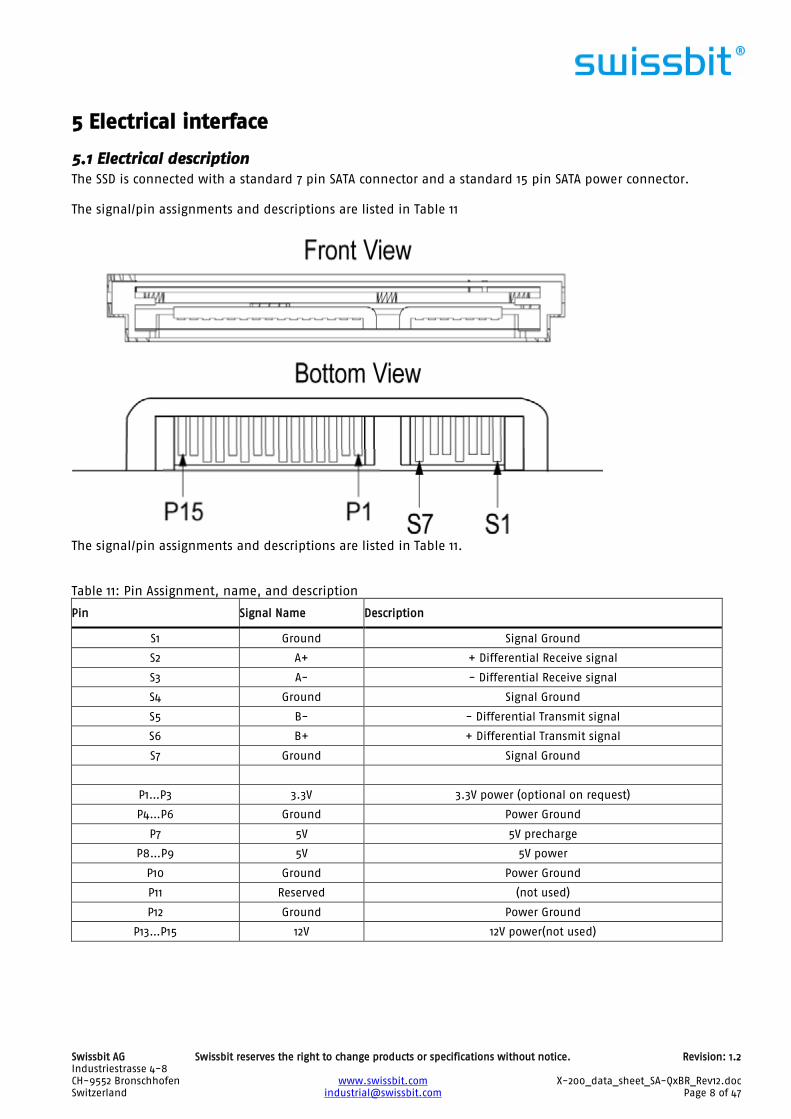
5 Electrical interface
5.1 Electrical description The SSD is connected with a standard 7 pin SATA connector and a standard 15 pin SATA power connector.
The signal/pin assignments and descriptions are listed in Table 11
The signal/pin assignments and descriptions are listed in Table 11.
Table 11: Pin Assignment, name, and description
Pin Signal Name Description
S1 Ground Signal Ground
S2 A+ + Differential Receive signal
S3 A- - Differential Receive signal
S4 Ground Signal Ground
S5 B- - Differential Transmit signal
S6 B+ + Differential Transmit signal
S7 Ground Signal Ground
P1…P3 3.3V 3.3V power (optional on request)
P4…P6 Ground Power Ground
P7 5V 5V precharge
P8…P9 5V 5V power
P10 Ground Power Ground
P11 Reserved (not used)
P12 Ground Power Ground
P13…P15 12V 12V power(not used)
Swissbit AG Swissbit reserves the right to change products or specifications without notice. Revision: 1.2 Industriestrasse 4-8
CH-9552 Bronschhofen www.swissbit.com X-200_data_sheet_SA-QxBR_Rev12.doc Switzerland [email protected] Page 9 of 47
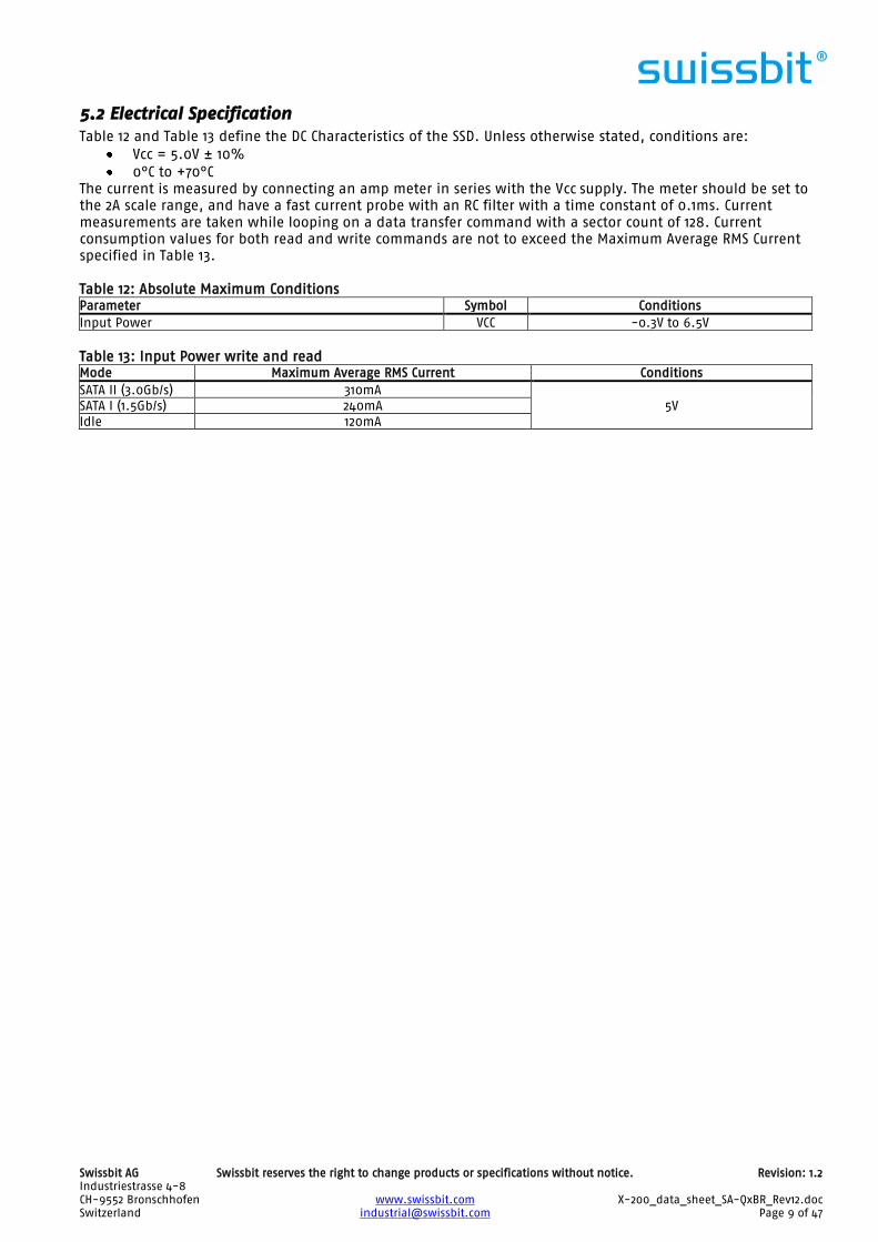
5.2 Electrical Specification Table 12 and Table 13 define the DC Characteristics of the SSD. Unless otherwise stated, conditions are:
Vcc = 5.0V ± 10%
0°C to +70°C
The current is measured by connecting an amp meter in series with the Vcc supply. The meter should be set to
the 2A scale range, and have a fast current probe with an RC filter with a time constant of 0.1ms. Current
measurements are taken while looping on a data transfer command with a sector count of 128. Current
consumption values for both read and write commands are not to exceed the Maximum Average RMS Current
specified in Table 13.
Table 12: Absolute Maximum Conditions Parameter Symbol Conditions
Input Power VCC -0.3V to 6.5V
Table 13: Input Power write and read Mode Maximum Average RMS Current Conditions
SATA II (3.0Gb/s) 310mA
5V SATA I (1.5Gb/s) 240mA
Idle 120mA
Swissbit AG Swissbit reserves the right to change products or specifications without notice. Revision: 1.2 Industriestrasse 4-8
CH-9552 Bronschhofen www.swissbit.com X-200_data_sheet_SA-QxBR_Rev12.doc Switzerland [email protected] Page 10 of 47
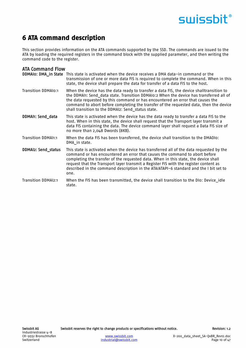
6 ATA command description
This section provides information on the ATA commands supported by the SSD. The commands are issued to the
ATA by loading the required registers in the command block with the supplied parameter, and then writing the
command code to the register.
ATA Command Flow DDMAI0: DMA_in State This state is activated when the device receives a DMA data-in command or the
transmission of one or more data FIS is required to complete the command. When in this
state, the device shall prepare the data for transfer of a data FIS to the host.
Transition DDMAI0:1 When the device has the data ready to transfer a data FIS, the device shalltransition to
the DDMAI1: Send_data state. Transition DDMAI0:2 When the device has transferred all of
the data requested by this command or has encountered an error that causes the
command to abort before completing the transfer of the requested data, then the device
shall transition to the DDMAI2: Send_status state.
DDMAI1: Send_data This state is activated when the device has the data ready to transfer a data FIS to the
host. When in this state, the device shall request that the Transport layer transmit a
data FIS containing the data. The device command layer shall request a Data FIS size of
no more than 2,048 Dwords (8KB).
Transition DDMAI1:1 When the data FIS has been transferred, the device shall transition to the DMAOI0:
DMA_in state.
DDMAI2: Send_status This state is activated when the device has transferred all of the data requested by the
command or has encountered an error that causes the command to abort before
completing the transfer of the requested data. When in this state, the device shall
request that the Transport layer transmit a Register FIS with the register content as
described in the command description in the ATA/ATAPI-6 standard and the I bit set to
one.
Transition DDMAI2:1 When the FIS has been transmitted, the device shall transition to the DI0: Device_idle
state.
Swissbit AG Swissbit reserves the right to change products or specifications without notice. Revision: 1.2 Industriestrasse 4-8
CH-9552 Bronschhofen www.swissbit.com X-200_data_sheet_SA-QxBR_Rev12.doc Switzerland [email protected] Page 11 of 47
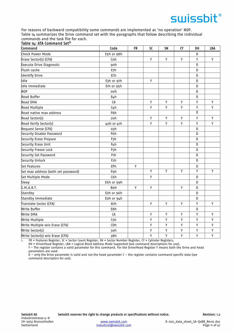
For reasons of backward compatibility some commands are implemented as ‘no operation’ NOP.
Table 14 summarizes the Drive command set with the paragraphs that follow describing the individual
commands and the task file for each.
Table 14: ATA Command Set(1)
Command Code FR SC SN CY DH LBA
Check Power Mode E5h or 98h D
Erase Sector(s) (CFA) C0h Y Y Y Y Y
Execute Drive Diagnostic 90h D
Flush cache E7h D
Identify Drive ECh D
Idle E3h or 97h Y D
Idle Immediate E1h or 95h D
NOP 00h D
Read Buffer E4h D
Read DMA C8 Y Y Y Y Y
Read Multiple C4h Y Y Y Y Y
Read native max address F8h D
Read Sector(s) 20h Y Y Y Y Y
Read Verify Sector(s) 40h or 41h Y Y Y Y Y
Request Sense (CFA) 03h D
Security Disable Password F6h D
Security Erase Prepare F3h D
Security Erase Unit F4h D
Security Freeze Lock F5h D
Security Set Password F1h D
Security Unlock F2h D
Set Features EFh Y D
Set max address (with set password) F9h Y Y Y Y Y
Set Multiple Mode C6h Y D
Sleep E6h or 99h D
S.M.A.R.T. B0h Y Y Y D
Standby E2h or 96h D
Standby Immediate E0h or 94h D
Translate Sector (CFA) 87h Y Y Y Y Y
Write Buffer E8h D
Write DMA CA Y Y Y Y Y
Write Multiple C5h Y Y Y Y Y
Write Multiple w/o Erase (CFA) CDh Y Y Y Y Y
Write Sector(s) 30h Y Y Y Y Y
Write Sector(s) w/o Erase (CFA) 38h Y Y Y Y Y
1. FR = Features Register, SC = Sector Count Register, SN = Sector Number Register, CY = Cylinder Registers,
DH = Drive/Head Register, LBA = Logical Block Address Mode Supported (see command descriptions for use), Y – The register contains a valid parameter for this command. For the Drive/Head Register Y means both the Drive and head
parameters are used. D – only the Drive parameter is valid and not the head parameter C – the register contains command specific data (see
command descriptors for use).
Swissbit AG Swissbit reserves the right to change products or specifications without notice. Revision: 1.2 Industriestrasse 4-8
CH-9552 Bronschhofen www.swissbit.com X-200_data_sheet_SA-QxBR_Rev12.doc Switzerland [email protected] Page 12 of 47
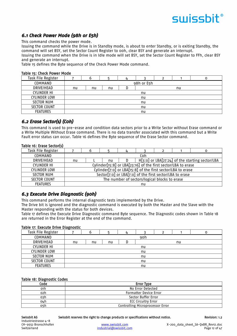
6.1 Check Power Mode (98h or E5h) This command checks the power mode.
Issuing the command while the Drive is in Standby mode, is about to enter Standby, or is exiting Standby, the
command will set BSY, set the Sector Count Register to 00h, clear BSY and generate an interrupt.
Issuing the command when the Drive is in Idle mode will set BSY, set the Sector Count Register to FFh, clear BSY
and generate an interrupt.
Table 15 defines the Byte sequence of the Check Power Mode command.
Table 15: Check Power Mode
Task File Register 7 6 5 4 3 2 1 0
COMMAND 98h or E5h
DRIVE/HEAD nu nu nu D nu
CYLINDER HI nu
CYLINDER LOW nu
SECTOR NUM nu
SECTOR COUNT nu
FEATURES nu
6.2 Erase Sector(s) (C0h) This command is used to pre-erase and condition data sectors prior to a Write Sector without Erase command or
a Write Multiple Without Erase command. There is no data transfer associated with this command but a Write
Fault error status can occur. Table 16 defines the Byte sequence of the Erase Sector command.
Table 16: Erase Sector(s)
Task File Register 7 6 5 4 3 2 1 0
COMMAND C0h
DRIVE/HEAD nu L nu D H[3:0] or LBA[27:24] of the starting sector/LBA
CYLINDER HI Cylinder[15:8] or LBA[23:16] of the first sector/LBA to erase
CYLINDER LOW Cylinder[7:0] or LBA[15:8] of the first sector/LBA to erase
SECTOR NUM Sector[7:0] or LBA[7:0] of the first sector/LBA to erase
SECTOR COUNT The number of sectors/logical blocks to erase
FEATURES nu
6.3 Execute Drive Diagnostic (90h) This command performs the internal diagnostic tests implemented by the Drive.
The Drive bit is ignored and the diagnostic command is executed by both the Master and the Slave with the
Master responding with the status for both devices.
Table 17 defines the Execute Drive Diagnostic command Byte sequence. The Diagnostic codes shown in Table 18 are returned in the Error Register at the end of the command.
Table 17: Execute Drive Diagnostic
Task File Register 7 6 5 4 3 2 1 0
COMMAND 90h
DRIVE/HEAD nu nu nu D nu
CYLINDER HI nu
CYLINDER LOW nu
SECTOR NUM nu
SECTOR COUNT nu
FEATURES nu
Table 18: Diagnostic Codes Code Error Type
01h No Error Detected
02h Formatter Device Error
03h Sector Buffer Error
04h ECC Circuitry Error
05h Controlling Microprocessor Error
Swissbit AG Swissbit reserves the right to change products or specifications without notice. Revision: 1.2 Industriestrasse 4-8
CH-9552 Bronschhofen www.swissbit.com X-200_data_sheet_SA-QxBR_Rev12.doc Switzerland [email protected] Page 13 of 47
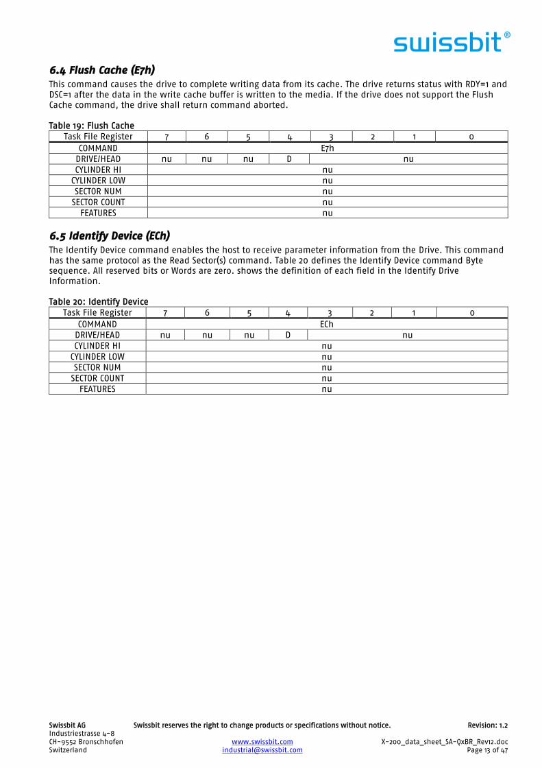
6.4 Flush Cache (E7h) This command causes the drive to complete writing data from its cache. The drive returns status with RDY=1 and
DSC=1 after the data in the write cache buffer is written to the media. If the drive does not support the Flush
Cache command, the drive shall return command aborted.
Table 19: Flush Cache
Task File Register 7 6 5 4 3 2 1 0
COMMAND E7h
DRIVE/HEAD nu nu nu D nu
CYLINDER HI nu
CYLINDER LOW nu
SECTOR NUM nu
SECTOR COUNT nu
FEATURES nu
6.5 Identify Device (ECh) The Identify Device command enables the host to receive parameter information from the Drive. This command
has the same protocol as the Read Sector(s) command. Table 20 defines the Identify Device command Byte
sequence. All reserved bits or Words are zero. shows the definition of each field in the Identify Drive
Information.
Table 20: Identify Device
Task File Register 7 6 5 4 3 2 1 0
COMMAND ECh
DRIVE/HEAD nu nu nu D nu
CYLINDER HI nu
CYLINDER LOW nu
SECTOR NUM nu
SECTOR COUNT nu
FEATURES nu
Swissbit AG Swissbit reserves the right to change products or specifications without notice. Revision: 1.2 Industriestrasse 4-8
CH-9552 Bronschhofen www.swissbit.com X-200_data_sheet_SA-QxBR_Rev12.doc Switzerland [email protected] Page 14 of 47
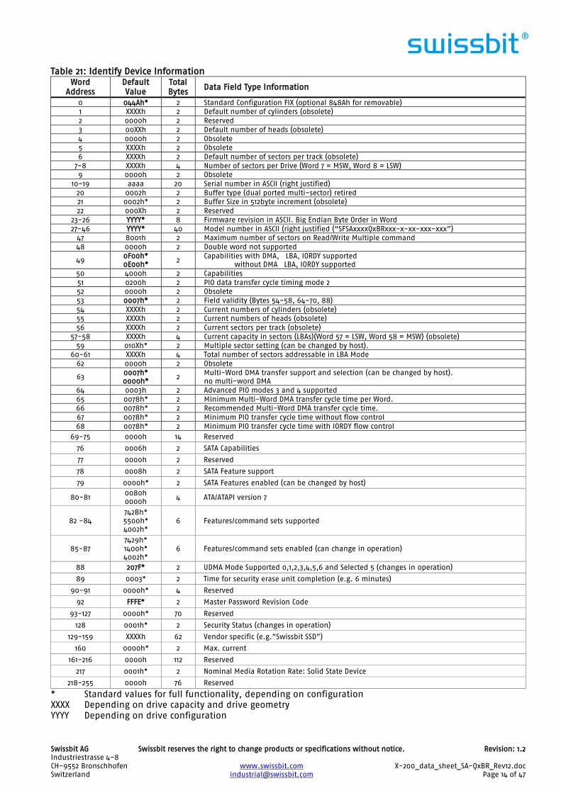
Table 21: Identify Device Information Word
Address
Default
Value
Total
Bytes Data Field Type Information
0 044Ah* 2 Standard Configuration FIX (optional 848Ah for removable)
1 XXXXh 2 Default number of cylinders (obsolete)
2 0000h 2 Reserved
3 00XXh 2 Default number of heads (obsolete)
4 0000h 2 Obsolete
5 XXXXh 2 Obsolete
6 XXXXh 2 Default number of sectors per track (obsolete)
7-8 XXXXh 4 Number of sectors per Drive (Word 7 = MSW, Word 8 = LSW)
9 0000h 2 Obsolete
10-19 aaaa 20 Serial number in ASCII (right justified)
20 0002h 2 Buffer type (dual ported multi-sector) retired
21 0002h* 2 Buffer Size in 512byte increment (obsolete)
22 000Xh 2 Reserved
23-26 YYYY* 8 Firmware revision in ASCII. Big Endian Byte Order in Word
27-46 YYYY* 40 Model number in ASCII (right justified (“SFSAxxxxQxBRxxx-x-xx-xxx-xxx”)
47 8001h 2 Maximum number of sectors on Read/Write Multiple command
48 0000h 2 Double word not supported
49 0F00h* 0E00h*
2 Capabilities with DMA, LBA, IORDY supported without DMA LBA, IORDY supported
50 4000h 2 Capabilities
51 0200h 2 PIO data transfer cycle timing mode 2
52 0000h 2 Obsolete
53 0007h* 2 Field validity (Bytes 54-58, 64-70, 88)
54 XXXXh 2 Current numbers of cylinders (obsolete)
55 XXXXh 2 Current numbers of heads (obsolete)
56 XXXXh 2 Current sectors per track (obsolete)
57-58 XXXXh 4 Current capacity in sectors (LBAs)(Word 57 = LSW, Word 58 = MSW) (obsolete)
59 010Xh* 2 Multiple sector setting (can be changed by host).
60-61 XXXXh 4 Total number of sectors addressable in LBA Mode
62 0000h 2 Obsolete
63 0007h* 0000h*
2 Multi-Word DMA transfer support and selection (can be changed by host). no multi-word DMA
64 0003h 2 Advanced PIO modes 3 and 4 supported
65 0078h* 2 Minimum Multi-Word DMA transfer cycle time per Word.
66 0078h* 2 Recommended Multi-Word DMA transfer cycle time.
67 0078h* 2 Minimum PIO transfer cycle time without flow control
68 0078h* 2 Minimum PIO transfer cycle time with IORDY flow control
69-75 0000h 14 Reserved
76 0006h 2 SATA Capabilities
77 0000h 2 Reserved
78 0008h 2 SATA Feature support
79 0000h* 2 SATA Features enabled (can be changed by host)
80-81 0080h 0000h
4 ATA/ATAPI version 7
82 -84
742Bh*
5500h* 4002h*
6 Features/command sets supported
85-87
7429h*
1400h* 4002h*
6 Features/command sets enabled (can change in operation)
88 207F* 2 UDMA Mode Supported 0,1,2,3,4,5,6 and Selected 5 (changes in operation)
89 0003* 2 Time for security erase unit completion (e.g. 6 minutes)
90-91 0000h* 4 Reserved
92 FFFE* 2 Master Password Revision Code
93-127 0000h* 70 Reserved
128 0001h* 2 Security Status (changes in operation)
129-159 XXXXh 62 Vendor specific (e.g.”Swissbit SSD”)
160 0000h* 2 Max. current
161-216 0000h 112 Reserved
217 0001h* 2 Nominal Media Rotation Rate: Solid State Device
218-255 0000h 76 Reserved
* Standard values for full functionality, depending on configuration
XXXX Depending on drive capacity and drive geometry
YYYY Depending on drive configuration
Swissbit AG Swissbit reserves the right to change products or specifications without notice. Revision: 1.2 Industriestrasse 4-8
CH-9552 Bronschhofen www.swissbit.com X-200_data_sheet_SA-QxBR_Rev12.doc Switzerland [email protected] Page 15 of 47
6.5.1 Word 0: General Configuration
This field indicates the general characteristics of the device.
The default value for Word 0 is set to 045Ah.
Some operating systems require Bit 6 of Word 0 to be set to ‘1’ (Non-removable device) to use the drive as the
root storage device.
6.5.2 Word 1: Default Number of Cylinders
This field contains the number of translated cylinders in the default translation mode. This value will be the
same as the number of cylinders.
6.5.3 Word 3: Default Number of Heads
This field contains the number of translated heads in the default translation mode.
6.5.4 Word 6: Default Number of Sectors per Track
This field contains the number of sectors per track in the default translation mode.
6.5.5 Word 7-8: Number of Sectors per Drive
This field contains the number of sectors per Drive. This double Word value is also the first invalid address in LBA
translation mode.
6.5.6 Word 10-19: Memory Drive Serial Number
The contents of this field are right justified and padded without spaces (20h).
6.5.7 Word 23-26: Firmware Revision
This field contains the revision of the firmware for this product.
6.5.8 Word 27-46: Model Number
This field contains the model number for this product and is left justified and padded with spaces (20h).
6.5.9 Word 47: Read/Write Multiple Sector Count
This field contains the maximum number of sectors that can be read or written per interrupt using the Read
Multiple or Write Multiple commands.
6.5.10 Word 49: Capabilities
Bit 13 Standby Timer: is set to ’0’ to indicate that the Standby timer operation is defined by the
manufacturer.
Bit 11: IORDY Supported
If bit 11 is set to 1 then this drive supports IORDY operation.
If bit 11 is set to 0 then this drive may support IORDY operation.
Bit 10: IORDY may be disabled
If bit 10 is set to 1 then IODRDY may be disabled.
Bit 9 LBA support: drive support LBA mode addressing.
Bit 8 DMA Support: Read/Write DMA commands are supported.
6.5.11 Word 51: PIO Data Transfer Cycle Timing Mode
This field defines the mode for PIO data transfer. For backward compatibility with BIOSs written before Word 64
was defined for advanced modes, a device reports in Word 51, the highest original PIO mode it can support (PIO
mode 0, 1 or 2). Bits 15-8: are set to 02H.
6.5.12 Word 53: Translation Parameter Valid
Bit 0: is set to ‘1’ to indicate that Words 54 to 58 are valid
Bit 1: is set to ‘1’ to indicate that Words 64 to 70 are valid
Bit 2 shall be set to 1 indicating that word 88 is valid and reflects the supported UDMA
Swissbit AG Swissbit reserves the right to change products or specifications without notice. Revision: 1.2 Industriestrasse 4-8
CH-9552 Bronschhofen www.swissbit.com X-200_data_sheet_SA-QxBR_Rev12.doc Switzerland [email protected] Page 16 of 47
6.5.13 Word 54-56: Current Number of Cylinders, Heads, Sectors/Track
These fields contain the current number of user addressable Cylinders, Heads, and Sectors/Track in the current
translation mode.
6.5.14 Word 57-58: Current Capacity
This field contains the product of the current cylinders, heads and sectors.
6.5.15 Word 59: Multiple Sector Setting
Bits 15-9 are reserved and must be set to ‘0’.
Bit 8 is set to ‘1’, to indicate that the Multiple Sector Setting is valid.
Bits 7-0 are the current setting for the number of sectors to be transferred for every interrupt, on
Read/Write Multiple commands; the only values returned are ‘00h’ or ‘01h’.
6.5.16 Word 60-61: Total Sectors Addressable in LBA Mode
This field contains the number of sectors addressable for the Drive in LBA mode only.
6.5.17 Word 63: Multi-Word DMA transfer
Bits 15 through 8 of word 63 of the Identify Device parameter information is defined as the Multiword DMA mode
selected field. If this field is supported, bit 1 of word 53 shall be set to one. This field is bit significant. Only one
of bits may be set to one in this field by the drive to indicate the multiword DMA mode which is currently
selected.
Of these bits, bits 15 through 11 are reserved. Bit 8, if set to one, indicates that Multiword DMA mode 0 has been
selected. Bit 9, if set to one, indicates that Multiword DMA mode 1 has been selected. Bit 10, if set to one,
indicates that Multiword DMA mode 2 has been selected.
Selection of Multiword DMA modes 3 and above are specific to Drive are as described in Word 163.
Bits 7 through 0 of word 63 of the Identify Device parameter information is defined as the Multiword DMA data
transfer supported field. If this field is supported, bit 1 of word 53 shall be set to one. This field is bit significant.
Any number of bits may be set to one in this field by the drive to indicate the Multiword DMA modes it is
capable of supporting.
Of these bits, bits 7 through 2 are reserved. Bit 0, if set to one, indicates that the drive supports Multiword DMA
mode 0. Bit 1, if set to one, indicates that the drive supports Multiword DMA modes 1 and 0. Bit 2, if set to one,
indicates that the Drive supports Multiword DMA modes 2, 1 and 0.
Support for Multiword DMA modes 3 and above are specific to Drive are reported in word 163 as described in
Word 163.
6.5.18 Word 64: Advanced PIO transfer modes supported
This field is bit significant. Any number of bits may be set to ‘1’ in this field by the drive to indicate the
advanced PIO modes it is capable of supporting.
Bits 7-2 are reserved for future advanced PIO modes.
Bit 1 is set to ‘1’, indicates that the Drive supports PIO mode 4.
Bit 0 is set to ‘1’ to indicate that the Drive supports PIO mode 3.
Support for PIO modes 5 and above are specific to Drive are reported in word 163 as described in Word 163.
6.5.19 Word 65: Minimum Multi-Word DMA transfer cycle time
Word 65 of the parameter information of the Identify Device command is defined as the minimum Multiword
DMA transfer cycle time. This field defines, in nanoseconds, the minimum cycle time that, if used by the host,
the Drive guarantees data integrity during the transfer.
If this field is supported, bit 1 of word 53 shall be set to one. The value in word 65 shall not be less than the
minimum cycle time for the fastest DMA mode supported by the device. This field shall be supported by all
Drives supporting DMA modes 1 and above. If bit 1 of word 53 is set to one, but this field is not supported, the
Drive shall return a value of zero in this field.
6.5.20 Word 66: Recommended Multi-Word DMA transfer cycle time
Word 66 of the parameter information of the Identify Device command is defined as the recommended
Multiword DMA transfer cycle time. This field defines, in nanoseconds, the cycle time that, if used by the host,
may optimize the data transfer from by reducing the probability that the Drive will need to negate the DMARQ
signal during the transfer of a sector.
Swissbit AG Swissbit reserves the right to change products or specifications without notice. Revision: 1.2 Industriestrasse 4-8
CH-9552 Bronschhofen www.swissbit.com X-200_data_sheet_SA-QxBR_Rev12.doc Switzerland [email protected] Page 17 of 47
If this field is supported, bit 1 of word 53 shall be set to one. The value in word 66 shall not be less than the
value in word 65. This field shall be supported by all Drives supporting DMA modes 1 and above. If bit 1 of word
53 is set to one, but this field is not supported, the Drive shall return a value of zero in this field.
6.5.21 Word 67: Minimum PIO transfer cycle time without flow control
Word 67 of the parameter information of the Identify Device command is defined as the minimum PIO transfer
without flow control cycle time. This field defines, in nanoseconds, the minimum cycle time that, if used by the
host, the Drive guarantees data integrity during the transfer without utilization of flow control.
If this field is supported, Bit 1 of word 53 shall be set to one.
Any Drive that supports PIO mode 3 or above shall support this field, and the value in word 67 shall not be less
than the value reported in word 68.
If bit 1 of word 53 is set to one because a Drive supports a field in words 64-70 other than this field and the
Drive does not support this field, the Drive shall return a value of zero in this field.
6.5.22 Word 68: Minimum PIO transfer cycle time with IORDY
Word 68 of the parameter information of the Identify Device command is defined as the minimum PIO transfer
with IORDY flow control cycle time. This field defines, in nanoseconds, the minimum cycle time that the Drive
supports while performing data transfers while utilizing IORDY flow control.
If this field is supported, Bit 1 of word 53 shall be set to one.
Any Drive that supports PIO mode 3 or above shall support this field, and the value in word 68 shall be the
fastest defined PIO mode supported by the Drive.
If bit 1 of word 53 is set to one because a Drive supports a field in words 64-70 other than this field and the
Drive does not support this field, the Drive shall return a value of zero in this field.
6.5.23 Word 76: Serial ATA Capabilities
Bit 15:11 Reserved
Bit 10 1 = Supports Phy Event Counters
Bit 9 1 = Supports receipt of host initiated power management requests
Bit 8 1 = Supports native Command Queuing
Bit 7:3 Reserved for future SATA signaling speed grades
Bit 2 1 = Supports SATA Gen2 Signaling Speed (3.0Gb/s)
Bit 1 1 = Supports SATA Gen1 Signaling Speed (1.5Gb/s)
Bit 0 Shall be cleared to zero
6.5.24 Word 78: SATA Feature support
Bit 15-7 Reserved
Bit 6 1 = Supports software settings preservation
Bit 5 1 = Supports asynchronous notification
Bit 4 1 = Supports in-order data delivery
Bit 3 1 = Device supports initiating interface power managment
Bit 2 1 = Supports DMA Setup Auto-Activate optimization
Bit 1 1 = Supports non-zero buffer offsets
Bit 0 Shall be cleared to zero
6.5.25 Word 79: SATA Features enabled
Bit 15-7 Reserved
Bit 6 1 = Supports software settings preservation enabled
Bit 5 1 = Supports asynchronous notification enabled
Bit 4 1 = Supports in-order data delivery enabled
Bit 3 1 = Device supports initiating interface power managment enabled
Bit 2 1 = Supports DMA Setup Auto-Activate optimization enabled
Bit 1 1 = Supports non-zero buffer offsets enabled
Bit 0 Shall be cleared to zero
Swissbit AG Swissbit reserves the right to change products or specifications without notice. Revision: 1.2 Industriestrasse 4-8
CH-9552 Bronschhofen www.swissbit.com X-200_data_sheet_SA-QxBR_Rev12.doc Switzerland [email protected] Page 18 of 47
6.5.26 Words 82-84: Features/command sets supported
Words 82, 83, and 84 shall indicate features/command sets supported. The value 0000h or FFFFh was placed in
each of these words by Drives prior to ATA-3 and shall be interpreted by the host as meaning that
features/command sets supported are not indicated. Bits 1 through 13 of word 83 and bits 0 through 13 of word
84 are reserved. Bit 14 of word 83 and word 84 shall be set to one and bit 15 of word 83 and word 84 shall be
cleared to zero to provide indication that the features/command sets supported words are valid. The values in
these words should not be depended on by host implementers.
Bit 0 of word 82 shall be set to zero; the SMART feature set is not supported.
If bit 1 of word 82 is set to one, the Security Mode feature set is supported.
Bit 2 of word 82 shall be set to zero; the Removable Media feature set is not supported.
Bit 3 of word 82 shall be set to one; the Power Management feature set is supported.
Bit 4 of word 82 shall be set to zero; the Packet Command feature set is not supported.
If bit 5 of word 82 is set to one, write cache is supported.
If bit 6 of word 82 is set to one, look-ahead is supported.
Bit 7 of word 82 shall be set to zero; release interrupt is not supported.
Bit 8 of word 82 shall be set to zero; Service interrupt is not supported.
Bit 9 of word 82 shall be set to zero; the Device Reset command is not supported.
Bit 10 of word 82 shall be set to zero; the Host Protected Area feature set is not supported.
Bit 11 of word 82 is obsolete.
Bit 12 of word 82 shall be set to one; the Drive supports the Write Buffer command.
Bit 13 of word 82 shall be set to one; the Drive supports the Read Buffer command.
Bit 14 of word 82 shall be set to one; the Drive supports the NOP command.
Bit 15 of word 82 is obsolete.
Bit 0 of word 83 shall be set to zero; the Drive does not support the Download Microcode command.
Bit 1 of word 83 shall be set to zero; the Drive does not support the Read DMA Queued and Write DMA
Queued commands.
Bit 2 of word 83 shall be set to zero; the Drive does not support the CFA feature set.
If bit 3 of word 83 is set to one, the Drive supports the Advanced Power Management feature set.
Bit 4 of word 83 shall be set to zero; the Drive does not support the Removable Media Status feature set.
6.5.27 Words 85-87: Features/command sets enabled
Words 85, 86, and 87 shall indicate features/command sets enabled. The value 0000h or FFFFh was placed in
each of these words by Drives prior to ATA-4 and shall be interpreted by the host as meaning that
features/command sets enabled are not indicated. Bits 1 through 15 of word 86 are reserved. Bits 0-13 of word
87 are reserved. Bit 14 of word 87 shall be set to one and bit 15 of word 87 shall be cleared to zero to provide
indication that the features/command sets enabled words are valid. The values in these words should not be
depended on by host implementers.
Bit 0 of word 85 shall be set to zero; the SMART feature set is not enabled.
If bit 1 of word 85 is set to one, the Security Mode feature set has been enabled via the Security
Set Password command.
Bit 2 of word 85 shall be set to zero; the Removable Media feature set is not supported.
Bit 3 of word 85 shall be set to one; the Power Management feature set is supported.
Bit 4 of word 85 shall be set to zero; the Packet Command feature set is not enabled.
If bit 5 of word 85 is set to one, write cache is enabled.
If bit 6 of word 85 is set to one, look-ahead is enabled.
Bit 7 of word 85 shall be set to zero; release interrupt is not enabled.
Bit 8 of word 85 shall be set to zero; Service interrupt is not enabled.
Bit 9 of word 85 shall be set to zero; the Device Reset command is not supported.
Bit 10 of word 85 shall be set to zero; the Host Protected Area feature set is not supported.
Bit 11 of word 85 is obsolete.
Bit 12 of word 85 shall be set to one; the Drive supports the Write Buffer command.
Bit 13 of word 85 shall be set to one; the Drive supports the Read Buffer command.
Bit 14 of word 85 shall be set to one; the Drive supports the NOP command.
Bit 15 of word 85 is obsolete.
Bit 0 of word 86 shall be set to zero; the Drive does not support the Download Microcode command.
Bit 1 of word 86 shall be set to zero; the Drive does not support the Read DMA Queued and Write DMA
Queued commands.
Swissbit AG Swissbit reserves the right to change products or specifications without notice. Revision: 1.2 Industriestrasse 4-8
CH-9552 Bronschhofen www.swissbit.com X-200_data_sheet_SA-QxBR_Rev12.doc Switzerland [email protected] Page 19 of 47
If bit 2 of word 86 shall be set to zero, the Drive does not support the CFA feature set.
If bit 3 of word 86 is set to one, the Advanced Power Management feature set has been enabled via the
Set Features command.
Bit 4 of word 86 shall be set to zero; the Drive does not support the Removable Media Status feature set.
6.5.28 Word 88: Ultra DMA Modes Supported and Selected
Word 88 identifies the Ultra DMA transfer modes supported by the device and indicates the mode that is
currently selected. Only one DMA mode shall be selected at any given time. If an Ultra DMA mode is selected,
then no Multiword DMA mode shall be selected. If a Multiword DMA mode is selected, then no Ultra DMA mode
shall be selected. Support of this word is mandatory if Ultra DMA is supported. Word 88 shall return a value of 0
if the device does not support UDMA.
Bit 15: Reserved
Bit 14: 1 = Ultra DMA mode 6 is selected 0 = Ultra DMA mode 6 is not selected
Bit 13: 1 = Ultra DMA mode 5 is selected 0 = Ultra DMA mode 5 is not selected
Bit 12: 1 = Ultra DMA mode 4 is selected 0 = Ultra DMA mode 4 is not selected
Bit 11: 1 = Ultra DMA mode 3 is selected 0 = Ultra DMA mode 3 is not selected
Bit 10: 1 = Ultra DMA mode 2 is selected 0 = Ultra DMA mode 2 is not selected
Bit 9: 1 = Ultra DMA mode 1 is selected 0 = Ultra DMA mode 1 is not selected
Bit 8: 1 = Ultra DMA mode 0 is selected 0 = Ultra DMA mode 0 is not selected
Bit 7: Reserved
Bit 6: 1 = Ultra DMA mode 6 and below are supported. Bits 0-5 shall be set to 1.
Bit 5: 1 = Ultra DMA mode 5 and below are supported. Bits 0-4 shall be set to 1.
Bit 4: 1 = Ultra DMA mode 4 and below are supported. Bits 0-3 shall be set to 1.
Bit 3: 1 = Ultra DMA mode 3 and below are supported, Bits 0-2 shall be set to 1.
Bit 2: 1 = Ultra DMA mode 2 and below are supported. Bits 0-1 shall be set to 1.
Bit 1: 1 = Ultra DMA mode 1 and below are supported. Bit 0 shall be set to 1.
Bit 0: 1 = Ultra DMA mode 0 is supported
6.5.29 Word 89: Time required for Security erase unit completion
Word 89 specifies the time required for the SECURITY ERASE UNIT command to complete. Support of this word is
mandatory if the Security feature set is supported.
Required Time=(Value*2) minutes
6.5.30 Word 92: Master Password Revision Code
Word 92 contains the value of the Master Password Revision Code set when the Master Password was last
changed. Valid values are 0001h through FFFEh. A value of 0000h or FFFFh indicates that the Master
Password Revision is not supported. Support of this word is mandatory if the Security feature set is
supported.
6.5.31 Word 128: Security status
Support of this word is mandatory if the Security feature set is supported.
Bit 8 of word 128 indicates the security level. If security mode is enabled and the security level is high, bit 8
shall be cleared to zero. If security mode is enabled and the security level is maximum, bit 8 shall be set to
one. When security mode is disabled, bit 8 shall be cleared to zero.
Bit 5 of word 128 indicates the Enhanced security erase unit feature is supported. If bit 5 is set to one, the
Enhanced security erase unit feature set is supported.
Bit 4 of word 128 indicates that the security count has expired. If bit 4 is set to one, the security count is expired
and SECURITY UNLOCK and SECURITY ERASE UNIT are command aborted until a power-on reset or hardware
reset.
Bit 3 of word 128 indicates security frozen. If bit 3 is set to one, the security is frozen.
Bit 2 of word 128 indicates security locked. If bit 2 is set to one, the security is locked.
Bit 1 of word 128 indicates security enabled. If bit 1 is set to one, the security is enabled.
Bit 0 of word 128 indicates the Security Mode feature set supported. If bit 0 is set to one, security is supported.
Swissbit AG Swissbit reserves the right to change products or specifications without notice. Revision: 1.2 Industriestrasse 4-8
CH-9552 Bronschhofen www.swissbit.com X-200_data_sheet_SA-QxBR_Rev12.doc Switzerland [email protected] Page 20 of 47
6.6 Idle (97h or E3h) This command causes the Drive to set BSY, enter the Idle mode, clear BSY and generate an interrupt. If the sector
count is non-zero, it is interpreted as a timer count (each count is 5ms) and the automatic power down mode is
enabled. If the sector count is zero, the automatic power down mode is disabled. Note that this time base (5ms)
is different from the ATA specification. Table 22 defines the Byte sequence of the Idle command.
Table 22: Idle
Task File Register 7 6 5 4 3 2 1 0
COMMAND 97h or E3h
DRIVE/HEAD nu nu nu D nu
CYLINDER HI nu
CYLINDER LOW nu
SECTOR NUM nu
SECTOR COUNT Timer Count (5ms increments)
FEATURES nu
6.7 Idle Immediate (95h or E1h) This command causes the Drive to set BSY, enter the Idle mode, clear BSY and generate an interrupt. Table 23 defines the Idle Immediate command Byte sequence.
Table 23: Idle Immediate
Task File Register 7 6 5 4 3 2 1 0
COMMAND 95h or E1h
DRIVE/HEAD nu nu nu D nu
CYLINDER HI nu
CYLINDER LOW nu
SECTOR NUM nu
SECTOR COUNT nu
FEATURES nu
6.8 NOP (00h) This command always fails with the Drive returning command aborted. Table 24 defines the Byte sequence of
the NOP command.
Table 24: NOP
Task File Register 7 6 5 4 3 2 1 0
COMMAND 00h
DRIVE/HEAD nu nu nu D nu
CYLINDER HI nu
CYLINDER LOW nu
SECTOR NUM nu
SECTOR COUNT nu
FEATURES nu
Swissbit AG Swissbit reserves the right to change products or specifications without notice. Revision: 1.2 Industriestrasse 4-8
CH-9552 Bronschhofen www.swissbit.com X-200_data_sheet_SA-QxBR_Rev12.doc Switzerland [email protected] Page 21 of 47
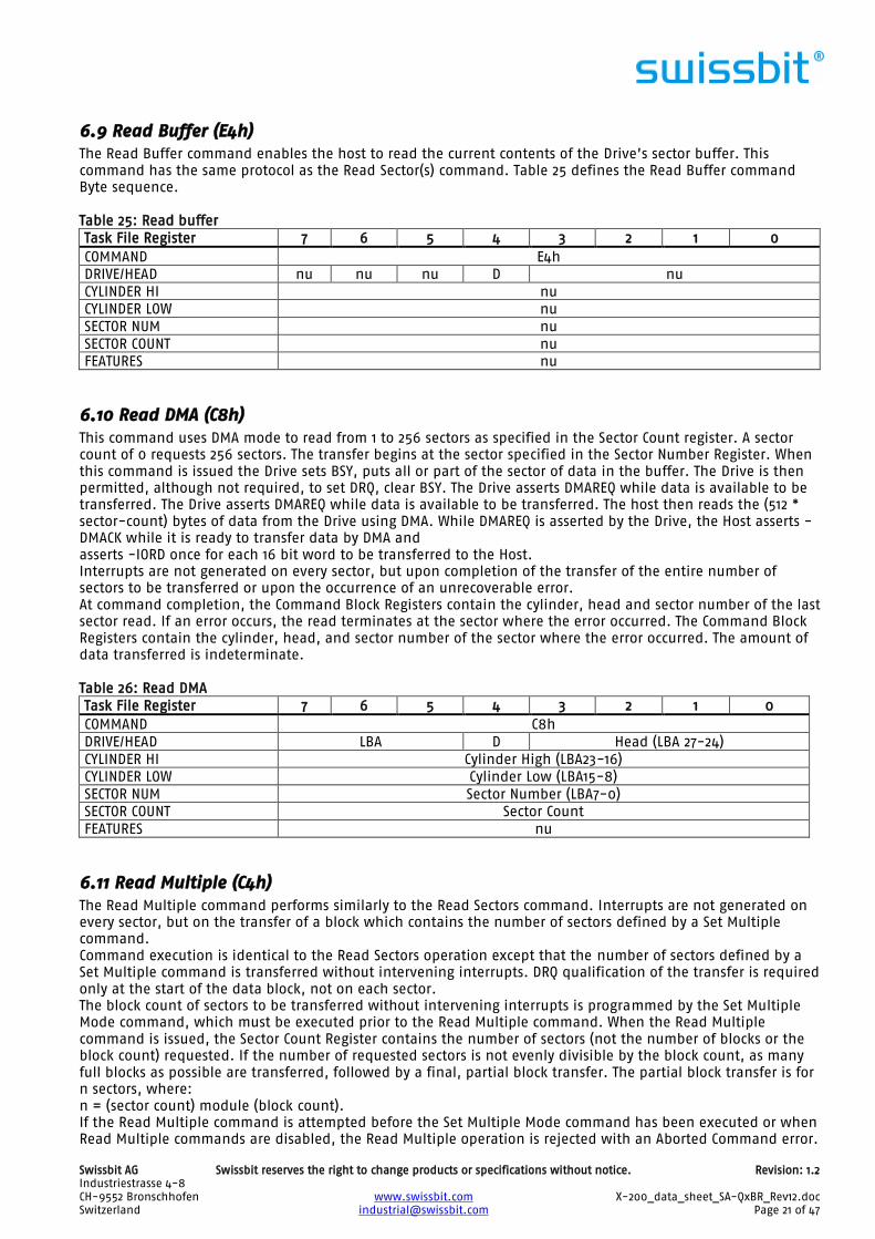
6.9 Read Buffer (E4h) The Read Buffer command enables the host to read the current contents of the Drive’s sector buffer. This
command has the same protocol as the Read Sector(s) command. Table 25 defines the Read Buffer command
Byte sequence.
Table 25: Read buffer
Task File Register 7 6 5 4 3 2 1 0
COMMAND E4h
DRIVE/HEAD nu nu nu D nu
CYLINDER HI nu
CYLINDER LOW nu
SECTOR NUM nu
SECTOR COUNT nu
FEATURES nu
6.10 Read DMA (C8h) This command uses DMA mode to read from 1 to 256 sectors as specified in the Sector Count register. A sector
count of 0 requests 256 sectors. The transfer begins at the sector specified in the Sector Number Register. When
this command is issued the Drive sets BSY, puts all or part of the sector of data in the buffer. The Drive is then
permitted, although not required, to set DRQ, clear BSY. The Drive asserts DMAREQ while data is available to be
transferred. The Drive asserts DMAREQ while data is available to be transferred. The host then reads the (512 *
sector-count) bytes of data from the Drive using DMA. While DMAREQ is asserted by the Drive, the Host asserts -
DMACK while it is ready to transfer data by DMA and
asserts -IORD once for each 16 bit word to be transferred to the Host.
Interrupts are not generated on every sector, but upon completion of the transfer of the entire number of
sectors to be transferred or upon the occurrence of an unrecoverable error.
At command completion, the Command Block Registers contain the cylinder, head and sector number of the last
sector read. If an error occurs, the read terminates at the sector where the error occurred. The Command Block
Registers contain the cylinder, head, and sector number of the sector where the error occurred. The amount of
data transferred is indeterminate.
Table 26: Read DMA
Task File Register 7 6 5 4 3 2 1 0
COMMAND C8h
DRIVE/HEAD LBA D Head (LBA 27-24)
CYLINDER HI Cylinder High (LBA23-16)
CYLINDER LOW Cylinder Low (LBA15-8)
SECTOR NUM Sector Number (LBA7-0)
SECTOR COUNT Sector Count
FEATURES nu
6.11 Read Multiple (C4h) The Read Multiple command performs similarly to the Read Sectors command. Interrupts are not generated on
every sector, but on the transfer of a block which contains the number of sectors defined by a Set Multiple
command.
Command execution is identical to the Read Sectors operation except that the number of sectors defined by a
Set Multiple command is transferred without intervening interrupts. DRQ qualification of the transfer is required
only at the start of the data block, not on each sector.
The block count of sectors to be transferred without intervening interrupts is programmed by the Set Multiple
Mode command, which must be executed prior to the Read Multiple command. When the Read Multiple
command is issued, the Sector Count Register contains the number of sectors (not the number of blocks or the
block count) requested. If the number of requested sectors is not evenly divisible by the block count, as many
full blocks as possible are transferred, followed by a final, partial block transfer. The partial block transfer is for
n sectors, where:
n = (sector count) module (block count).
If the Read Multiple command is attempted before the Set Multiple Mode command has been executed or when
Read Multiple commands are disabled, the Read Multiple operation is rejected with an Aborted Command error.
Swissbit AG Swissbit reserves the right to change products or specifications without notice. Revision: 1.2 Industriestrasse 4-8
CH-9552 Bronschhofen www.swissbit.com X-200_data_sheet_SA-QxBR_Rev12.doc Switzerland [email protected] Page 22 of 47
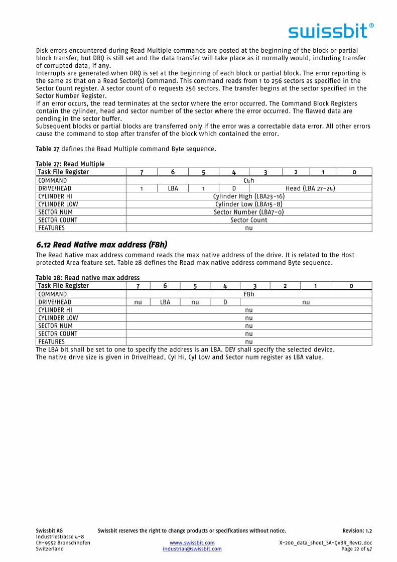
Disk errors encountered during Read Multiple commands are posted at the beginning of the block or partial
block transfer, but DRQ is still set and the data transfer will take place as it normally would, including transfer
of corrupted data, if any.
Interrupts are generated when DRQ is set at the beginning of each block or partial block. The error reporting is
the same as that on a Read Sector(s) Command. This command reads from 1 to 256 sectors as specified in the
Sector Count register. A sector count of 0 requests 256 sectors. The transfer begins at the sector specified in the
Sector Number Register.
If an error occurs, the read terminates at the sector where the error occurred. The Command Block Registers
contain the cylinder, head and sector number of the sector where the error occurred. The flawed data are
pending in the sector buffer.
Subsequent blocks or partial blocks are transferred only if the error was a correctable data error. All other errors
cause the command to stop after transfer of the block which contained the error.
Table 27 defines the Read Multiple command Byte sequence.
Table 27: Read Multiple
Task File Register 7 6 5 4 3 2 1 0
COMMAND C4h
DRIVE/HEAD 1 LBA 1 D Head (LBA 27-24)
CYLINDER HI Cylinder High (LBA23-16)
CYLINDER LOW Cylinder Low (LBA15-8)
SECTOR NUM Sector Number (LBA7-0)
SECTOR COUNT Sector Count
FEATURES nu
6.12 Read Native max address (F8h) The Read Native max address command reads the max native address of the drive. It is related to the Host
protected Area feature set. Table 28 defines the Read max native address command Byte sequence.
Table 28: Read native max address
Task File Register 7 6 5 4 3 2 1 0
COMMAND F8h
DRIVE/HEAD nu LBA nu D nu
CYLINDER HI nu
CYLINDER LOW nu
SECTOR NUM nu
SECTOR COUNT nu
FEATURES nu
The LBA bit shall be set to one to specify the address is an LBA. DEV shall specify the selected device.
The native drive size is given in Drive/Head, Cyl Hi, Cyl Low and Sector num register as LBA value.
Swissbit AG Swissbit reserves the right to change products or specifications without notice. Revision: 1.2 Industriestrasse 4-8
CH-9552 Bronschhofen www.swissbit.com X-200_data_sheet_SA-QxBR_Rev12.doc Switzerland [email protected] Page 23 of 47
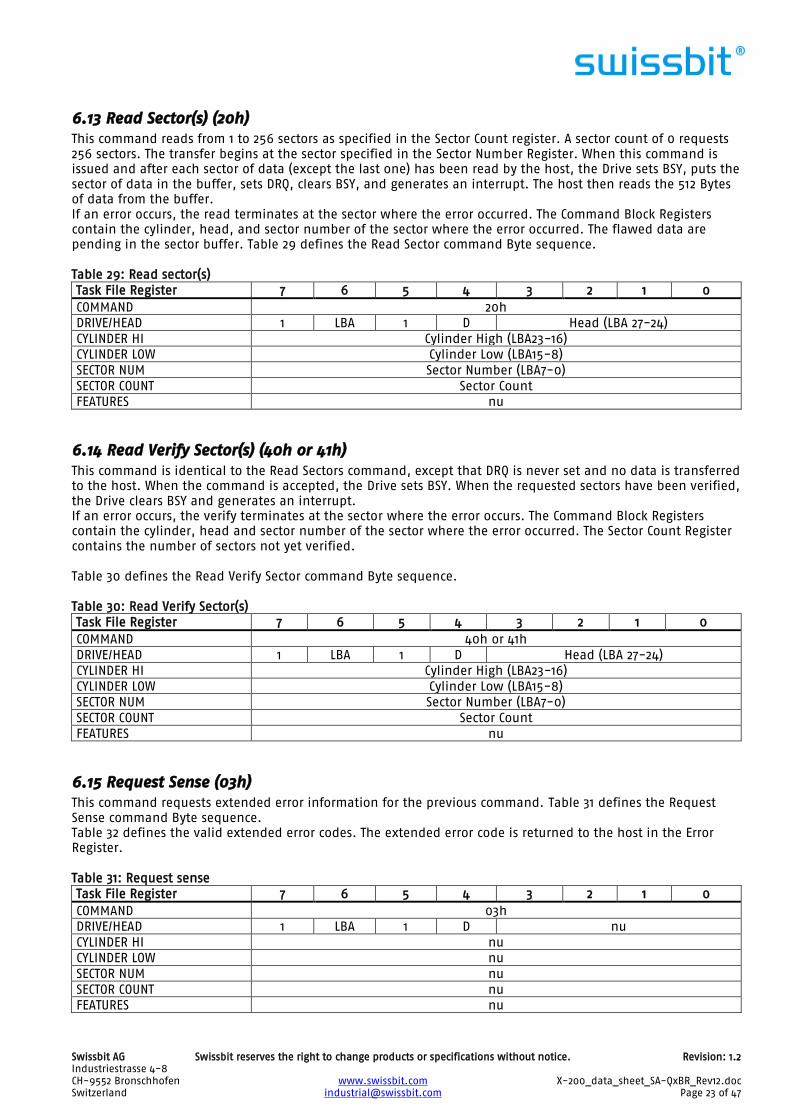
6.13 Read Sector(s) (20h) This command reads from 1 to 256 sectors as specified in the Sector Count register. A sector count of 0 requests
256 sectors. The transfer begins at the sector specified in the Sector Number Register. When this command is
issued and after each sector of data (except the last one) has been read by the host, the Drive sets BSY, puts the
sector of data in the buffer, sets DRQ, clears BSY, and generates an interrupt. The host then reads the 512 Bytes
of data from the buffer.
If an error occurs, the read terminates at the sector where the error occurred. The Command Block Registers
contain the cylinder, head, and sector number of the sector where the error occurred. The flawed data are
pending in the sector buffer. Table 29 defines the Read Sector command Byte sequence.
Table 29: Read sector(s)
Task File Register 7 6 5 4 3 2 1 0
COMMAND 20h
DRIVE/HEAD 1 LBA 1 D Head (LBA 27-24)
CYLINDER HI Cylinder High (LBA23-16)
CYLINDER LOW Cylinder Low (LBA15-8)
SECTOR NUM Sector Number (LBA7-0)
SECTOR COUNT Sector Count
FEATURES nu
6.14 Read Verify Sector(s) (40h or 41h) This command is identical to the Read Sectors command, except that DRQ is never set and no data is transferred
to the host. When the command is accepted, the Drive sets BSY. When the requested sectors have been verified,
the Drive clears BSY and generates an interrupt.
If an error occurs, the verify terminates at the sector where the error occurs. The Command Block Registers
contain the cylinder, head and sector number of the sector where the error occurred. The Sector Count Register
contains the number of sectors not yet verified.
Table 30 defines the Read Verify Sector command Byte sequence.
Table 30: Read Verify Sector(s)
Task File Register 7 6 5 4 3 2 1 0
COMMAND 40h or 41h
DRIVE/HEAD 1 LBA 1 D Head (LBA 27-24)
CYLINDER HI Cylinder High (LBA23-16)
CYLINDER LOW Cylinder Low (LBA15-8)
SECTOR NUM Sector Number (LBA7-0)
SECTOR COUNT Sector Count
FEATURES nu
6.15 Request Sense (03h) This command requests extended error information for the previous command. Table 31 defines the Request
Sense command Byte sequence.
Table 32 defines the valid extended error codes. The extended error code is returned to the host in the Error
Register.
Table 31: Request sense
Task File Register 7 6 5 4 3 2 1 0
COMMAND 03h
DRIVE/HEAD 1 LBA 1 D nu
CYLINDER HI nu
CYLINDER LOW nu
SECTOR NUM nu
SECTOR COUNT nu
FEATURES nu
Swissbit AG Swissbit reserves the right to change products or specifications without notice. Revision: 1.2 Industriestrasse 4-8
CH-9552 Bronschhofen www.swissbit.com X-200_data_sheet_SA-QxBR_Rev12.doc Switzerland [email protected] Page 24 of 47
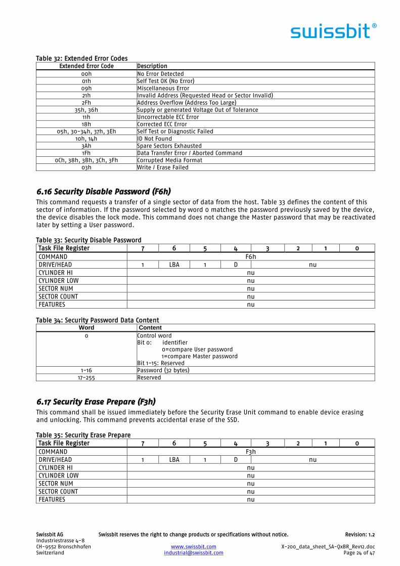
Table 32: Extended Error Codes Extended Error Code Description
00h No Error Detected
01h Self Test OK (No Error)
09h Miscellaneous Error
21h Invalid Address (Requested Head or Sector Invalid)
2Fh Address Overflow (Address Too Large)
35h, 36h Supply or generated Voltage Out of Tolerance
11h Uncorrectable ECC Error
18h Corrected ECC Error
05h, 30-34h, 37h, 3Eh Self Test or Diagnostic Failed
10h, 14h ID Not Found
3Ah Spare Sectors Exhausted
1Fh Data Transfer Error / Aborted Command
0Ch, 38h, 3Bh, 3Ch, 3Fh Corrupted Media Format
03h Write / Erase Failed
6.16 Security Disable Password (F6h) This command requests a transfer of a single sector of data from the host. Table 33 defines the content of this
sector of information. If the password selected by word 0 matches the password previously saved by the device,
the device disables the lock mode. This command does not change the Master password that may be reactivated
later by setting a User password.
Table 33: Security Disable Password
Task File Register 7 6 5 4 3 2 1 0
COMMAND F6h
DRIVE/HEAD 1 LBA 1 D nu
CYLINDER HI nu
CYLINDER LOW nu
SECTOR NUM nu
SECTOR COUNT nu
FEATURES nu
Table 34: Security Password Data Content
Word Content
0 Control word Bit 0: identifier
0=compare User password
1=compare Master password
Bit 1-15: Reserved
1-16 Password (32 bytes)
17-255 Reserved
6.17 Security Erase Prepare (F3h) This command shall be issued immediately before the Security Erase Unit command to enable device erasing
and unlocking. This command prevents accidental erase of the SSD.
Table 35: Security Erase Prepare
Task File Register 7 6 5 4 3 2 1 0
COMMAND F3h
DRIVE/HEAD 1 LBA 1 D nu
CYLINDER HI nu
CYLINDER LOW nu
SECTOR NUM nu
SECTOR COUNT nu
FEATURES nu
Swissbit AG Swissbit reserves the right to change products or specifications without notice. Revision: 1.2 Industriestrasse 4-8
CH-9552 Bronschhofen www.swissbit.com X-200_data_sheet_SA-QxBR_Rev12.doc Switzerland [email protected] Page 25 of 47
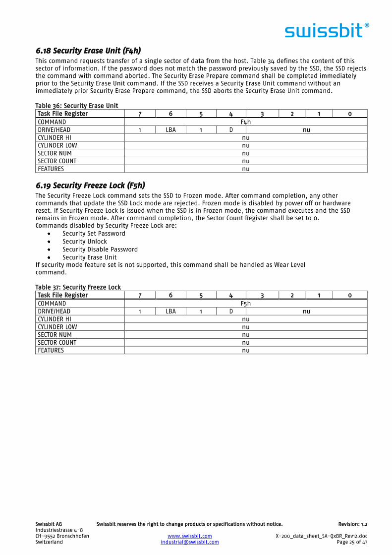
6.18 Security Erase Unit (F4h) This command requests transfer of a single sector of data from the host. Table 34 defines the content of this
sector of information. If the password does not match the password previously saved by the SSD, the SSD rejects
the command with command aborted. The Security Erase Prepare command shall be completed immediately
prior to the Security Erase Unit command. If the SSD receives a Security Erase Unit command without an
immediately prior Security Erase Prepare command, the SSD aborts the Security Erase Unit command.
Table 36: Security Erase Unit
Task File Register 7 6 5 4 3 2 1 0
COMMAND F4h
DRIVE/HEAD 1 LBA 1 D nu
CYLINDER HI nu
CYLINDER LOW nu
SECTOR NUM nu
SECTOR COUNT nu
FEATURES nu
6.19 Security Freeze Lock (F5h) The Security Freeze Lock command sets the SSD to Frozen mode. After command completion, any other
commands that update the SSD Lock mode are rejected. Frozen mode is disabled by power off or hardware
reset. If Security Freeze Lock is issued when the SSD is in Frozen mode, the command executes and the SSD
remains in Frozen mode. After command completion, the Sector Count Register shall be set to 0.
Commands disabled by Security Freeze Lock are:
� Security Set Password
� Security Unlock
� Security Disable Password
� Security Erase Unit
If security mode feature set is not supported, this command shall be handled as Wear Level
command.
Table 37: Security Freeze Lock
Task File Register 7 6 5 4 3 2 1 0
COMMAND F5h
DRIVE/HEAD 1 LBA 1 D nu
CYLINDER HI nu
CYLINDER LOW nu
SECTOR NUM nu
SECTOR COUNT nu
FEATURES nu
Swissbit AG Swissbit reserves the right to change products or specifications without notice. Revision: 1.2 Industriestrasse 4-8
CH-9552 Bronschhofen www.swissbit.com X-200_data_sheet_SA-QxBR_Rev12.doc Switzerland [email protected] Page 26 of 47
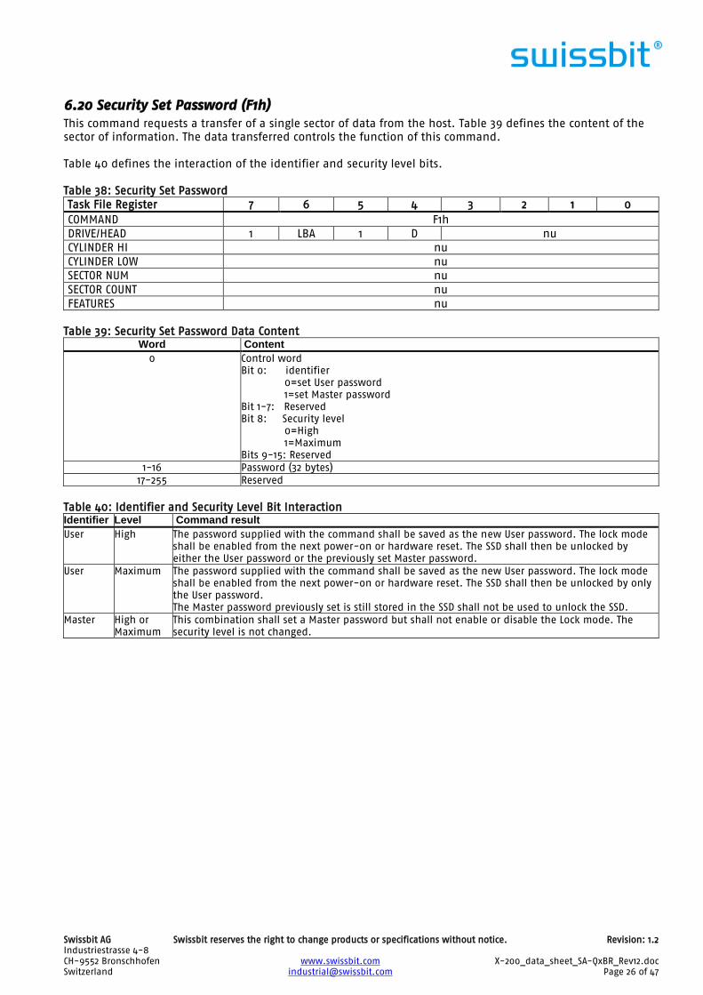
6.20 Security Set Password (F1h) This command requests a transfer of a single sector of data from the host. Table 39 defines the content of the
sector of information. The data transferred controls the function of this command.
Table 40 defines the interaction of the identifier and security level bits.
Table 38: Security Set Password
Task File Register 7 6 5 4 3 2 1 0
COMMAND F1h
DRIVE/HEAD 1 LBA 1 D nu
CYLINDER HI nu
CYLINDER LOW nu
SECTOR NUM nu
SECTOR COUNT nu
FEATURES nu
Table 39: Security Set Password Data Content
Word Content
0 Control word Bit 0: identifier
0=set User password
1=set Master password
Bit 1-7: Reserved
Bit 8: Security level
0=High
1=Maximum
Bits 9-15: Reserved
1-16 Password (32 bytes)
17-255 Reserved
Table 40: Identifier and Security Level Bit Interaction Identifier Level Command result
User High The password supplied with the command shall be saved as the new User password. The lock mode
shall be enabled from the next power-on or hardware reset. The SSD shall then be unlocked by
either the User password or the previously set Master password.
User Maximum The password supplied with the command shall be saved as the new User password. The lock mode
shall be enabled from the next power-on or hardware reset. The SSD shall then be unlocked by only
the User password.
The Master password previously set is still stored in the SSD shall not be used to unlock the SSD.
Master High or
Maximum
This combination shall set a Master password but shall not enable or disable the Lock mode. The
security level is not changed.
Swissbit AG Swissbit reserves the right to change products or specifications without notice. Revision: 1.2 Industriestrasse 4-8
CH-9552 Bronschhofen www.swissbit.com X-200_data_sheet_SA-QxBR_Rev12.doc Switzerland [email protected] Page 27 of 47
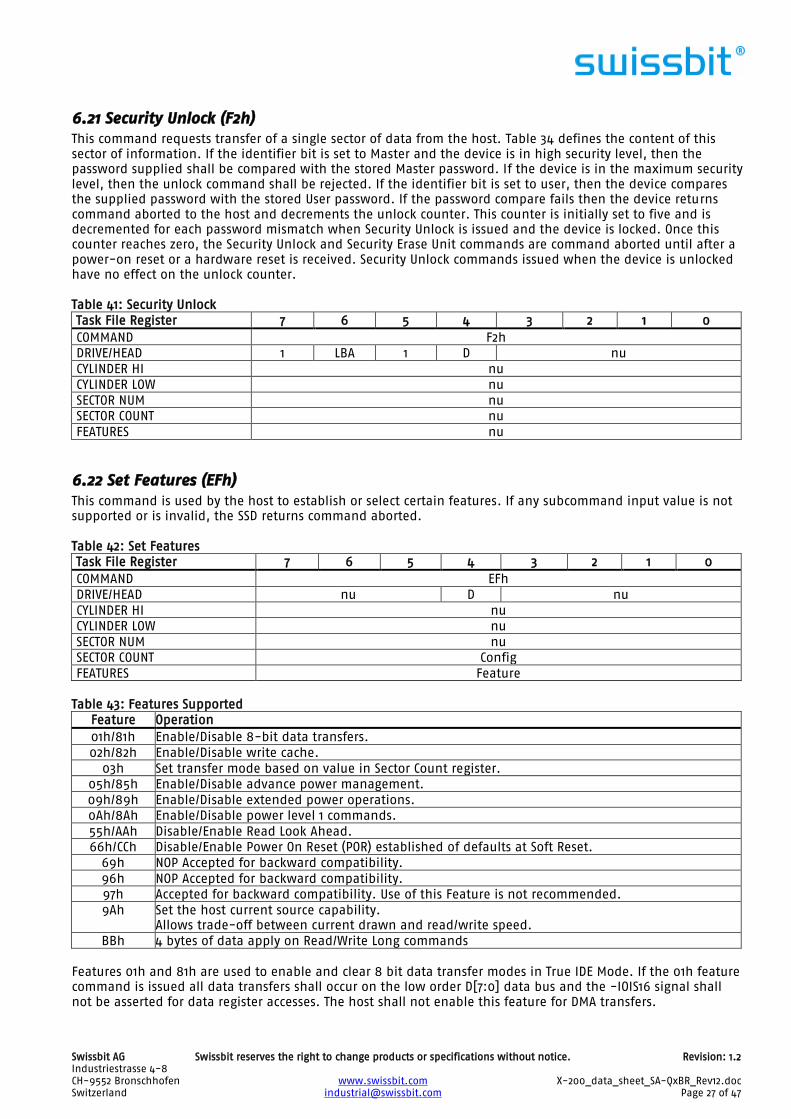
6.21 Security Unlock (F2h) This command requests transfer of a single sector of data from the host. Table 34 defines the content of this
sector of information. If the identifier bit is set to Master and the device is in high security level, then the
password supplied shall be compared with the stored Master password. If the device is in the maximum security
level, then the unlock command shall be rejected. If the identifier bit is set to user, then the device compares
the supplied password with the stored User password. If the password compare fails then the device returns
command aborted to the host and decrements the unlock counter. This counter is initially set to five and is
decremented for each password mismatch when Security Unlock is issued and the device is locked. Once this
counter reaches zero, the Security Unlock and Security Erase Unit commands are command aborted until after a
power-on reset or a hardware reset is received. Security Unlock commands issued when the device is unlocked
have no effect on the unlock counter.
Table 41: Security Unlock
Task File Register 7 6 5 4 3 2 1 0
COMMAND F2h
DRIVE/HEAD 1 LBA 1 D nu
CYLINDER HI nu
CYLINDER LOW nu
SECTOR NUM nu
SECTOR COUNT nu
FEATURES nu
6.22 Set Features (EFh) This command is used by the host to establish or select certain features. If any subcommand input value is not
supported or is invalid, the SSD returns command aborted.
Table 42: Set Features
Task File Register 7 6 5 4 3 2 1 0
COMMAND EFh
DRIVE/HEAD nu D nu
CYLINDER HI nu
CYLINDER LOW nu
SECTOR NUM nu
SECTOR COUNT Config
FEATURES Feature
Table 43: Features Supported
Feature Operation
01h/81h Enable/Disable 8-bit data transfers.
02h/82h Enable/Disable write cache.
03h Set transfer mode based on value in Sector Count register.
05h/85h Enable/Disable advance power management.
09h/89h Enable/Disable extended power operations.
0Ah/8Ah Enable/Disable power level 1 commands.
55h/AAh Disable/Enable Read Look Ahead.
66h/CCh Disable/Enable Power On Reset (POR) established of defaults at Soft Reset.
69h NOP Accepted for backward compatibility.
96h NOP Accepted for backward compatibility.
97h Accepted for backward compatibility. Use of this Feature is not recommended.
9Ah Set the host current source capability.
Allows trade-off between current drawn and read/write speed.
BBh 4 bytes of data apply on Read/Write Long commands
Features 01h and 81h are used to enable and clear 8 bit data transfer modes in True IDE Mode. If the 01h feature
command is issued all data transfers shall occur on the low order D[7:0] data bus and the -IOIS16 signal shall
not be asserted for data register accesses. The host shall not enable this feature for DMA transfers.
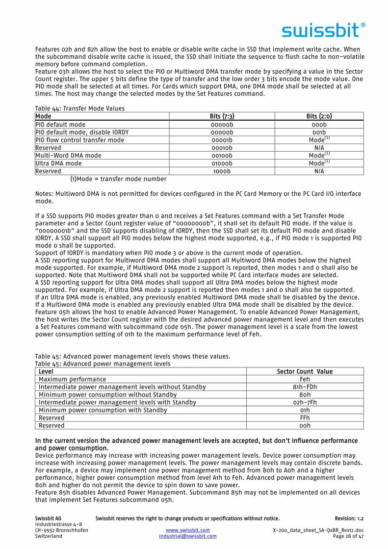
Swissbit AG Swissbit reserves the right to change products or specifications without notice. Revision: 1.2 Industriestrasse 4-8
CH-9552 Bronschhofen www.swissbit.com X-200_data_sheet_SA-QxBR_Rev12.doc Switzerland [email protected] Page 28 of 47
Features 02h and 82h allow the host to enable or disable write cache in SSD that implement write cache. When
the subcommand disable write cache is issued, the SSD shall initiate the sequence to flush cache to non-volatile
memory before command completion.
Feature 03h allows the host to select the PIO or Multiword DMA transfer mode by specifying a value in the Sector
Count register. The upper 5 bits define the type of transfer and the low order 3 bits encode the mode value. One
PIO mode shall be selected at all times. For Cards which support DMA, one DMA mode shall be selected at all
times. The host may change the selected modes by the Set Features command.
Table 44: Transfer Mode Values
Mode Bits (7:3) Bits (2:0)
PIO default mode 00000b 000b
PIO default mode, disable IORDY 00000b 001b
PIO flow control transfer mode 00001b Mode(1)
Reserved 00010b N/A
Multi-Word DMA mode 00100b Mode(1)
Ultra DMA mode 01000b Mode(1)
Reserved 1000b N/A
(1)Mode = transfer mode number
Notes: Multiword DMA is not permitted for devices configured in the PC Card Memory or the PC Card I/O interface
mode.
If a SSD supports PIO modes greater than 0 and receives a Set Features command with a Set Transfer Mode
parameter and a Sector Count register value of “00000000b”, it shall set its default PIO mode. If the value is
“00000001b” and the SSD supports disabling of IORDY, then the SSD shall set its default PIO mode and disable
IORDY. A SSD shall support all PIO modes below the highest mode supported, e.g., if PIO mode 1 is supported PIO
mode 0 shall be supported.
Support of IORDY is mandatory when PIO mode 3 or above is the current mode of operation.
A SSD reporting support for Multiword DMA modes shall support all Multiword DMA modes below the highest
mode supported. For example, if Multiword DMA mode 2 support is reported, then modes 1 and 0 shall also be
supported. Note that Multiword DMA shall not be supported while PC Card interface modes are selected.
A SSD reporting support for Ultra DMA modes shall support all Ultra DMA modes below the highest mode
supported. For example, if Ultra DMA mode 2 support is reported then modes 1 and 0 shall also be supported.
If an Ultra DMA mode is enabled, any previously enabled Multiword DMA mode shall be disabled by the device.
If a Multiword DMA mode is enabled any previously enabled Ultra DMA mode shall be disabled by the device.
Feature 05h allows the host to enable Advanced Power Management. To enable Advanced Power Management,
the host writes the Sector Count register with the desired advanced power management level and then executes
a Set Features command with subcommand code 05h. The power management level is a scale from the lowest
power consumption setting of 01h to the maximum performance level of Feh.
Table 45: Advanced power management levels shows these values.
Table 45: Advanced power management levels
Level Sector Count Value
Maximum performance Feh
Intermediate power management levels without Standby 81h-FDh
Minimum power consumption without Standby 80h
Intermediate power management levels with Standby 02h-7Fh
Minimum power consumption with Standby 01h
Reserved FFh
Reserved 00h
In the current version the advanced power management levels are accepted, but don’t influence performance
and power consumption.
Device performance may increase with increasing power management levels. Device power consumption may
increase with increasing power management levels. The power management levels may contain discrete bands.
For example, a device may implement one power management method from 80h to A0h and a higher
performance, higher power consumption method from level A1h to Feh. Advanced power management levels
80h and higher do not permit the device to spin down to save power.
Feature 85h disables Advanced Power Management. Subcommand 85h may not be implemented on all devices
that implement Set Features subcommand 05h.
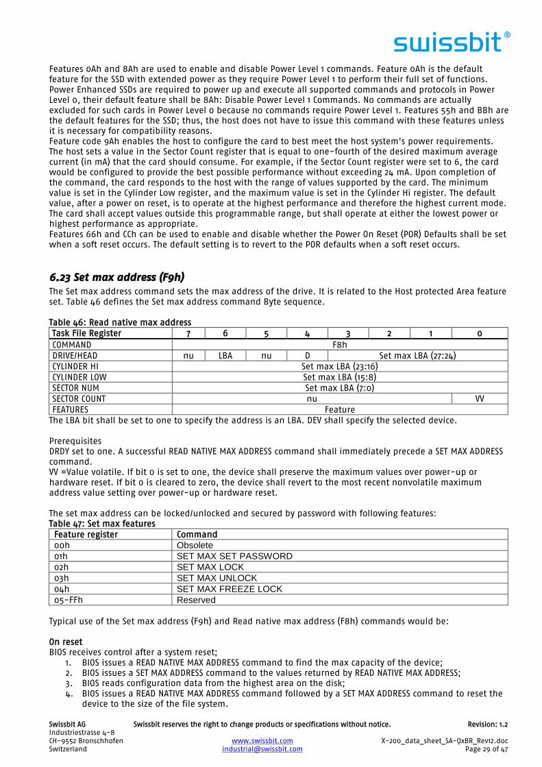
Swissbit AG Swissbit reserves the right to change products or specifications without notice. Revision: 1.2 Industriestrasse 4-8
CH-9552 Bronschhofen www.swissbit.com X-200_data_sheet_SA-QxBR_Rev12.doc Switzerland [email protected] Page 29 of 47
Features 0Ah and 8Ah are used to enable and disable Power Level 1 commands. Feature 0Ah is the default
feature for the SSD with extended power as they require Power Level 1 to perform their full set of functions.
Power Enhanced SSDs are required to power up and execute all supported commands and protocols in Power
Level 0, their default feature shall be 8Ah: Disable Power Level 1 Commands. No commands are actually
excluded for such cards in Power Level 0 because no commands require Power Level 1. Features 55h and BBh are
the default features for the SSD; thus, the host does not have to issue this command with these features unless
it is necessary for compatibility reasons.
Feature code 9Ah enables the host to configure the card to best meet the host system’s power requirements.
The host sets a value in the Sector Count register that is equal to one-fourth of the desired maximum average
current (in mA) that the card should consume. For example, if the Sector Count register were set to 6, the card
would be configured to provide the best possible performance without exceeding 24 mA. Upon completion of
the command, the card responds to the host with the range of values supported by the card. The minimum
value is set in the Cylinder Low register, and the maximum value is set in the Cylinder Hi register. The default
value, after a power on reset, is to operate at the highest performance and therefore the highest current mode.
The card shall accept values outside this programmable range, but shall operate at either the lowest power or
highest performance as appropriate.
Features 66h and CCh can be used to enable and disable whether the Power On Reset (POR) Defaults shall be set
when a soft reset occurs. The default setting is to revert to the POR defaults when a soft reset occurs.
6.23 Set max address (F9h) The Set max address command sets the max address of the drive. It is related to the Host protected Area feature
set. Table 46 defines the Set max address command Byte sequence.
Table 46: Read native max address
Task File Register 7 6 5 4 3 2 1 0
COMMAND F8h
DRIVE/HEAD nu LBA nu D Set max LBA (27:24)
CYLINDER HI Set max LBA (23:16)
CYLINDER LOW Set max LBA (15:8)
SECTOR NUM Set max LBA (7:0)
SECTOR COUNT nu VV
FEATURES Feature
The LBA bit shall be set to one to specify the address is an LBA. DEV shall specify the selected device.
Prerequisites
DRDY set to one. A successful READ NATIVE MAX ADDRESS command shall immediately precede a SET MAX ADDRESS
command.
VV =Value volatile. If bit 0 is set to one, the device shall preserve the maximum values over power-up or
hardware reset. If bit 0 is cleared to zero, the device shall revert to the most recent nonvolatile maximum
address value setting over power-up or hardware reset.
The set max address can be locked/unlocked and secured by password with following features:
Table 47: Set max features
Feature register Command
00h Obsolete
01h SET MAX SET PASSWORD
02h SET MAX LOCK
03h SET MAX UNLOCK
04h SET MAX FREEZE LOCK
05-FFh Reserved
Typical use of the Set max address (F9h) and Read native max address (F8h) commands would be:
On reset
BIOS receives control after a system reset;
1. BIOS issues a READ NATIVE MAX ADDRESS command to find the max capacity of the device;
2. BIOS issues a SET MAX ADDRESS command to the values returned by READ NATIVE MAX ADDRESS;
3. BIOS reads configuration data from the highest area on the disk;
4. BIOS issues a READ NATIVE MAX ADDRESS command followed by a SET MAX ADDRESS command to reset the
device to the size of the file system.
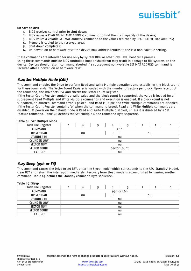
Swissbit AG Swissbit reserves the right to change products or specifications without notice. Revision: 1.2 Industriestrasse 4-8
CH-9552 Bronschhofen www.swissbit.com X-200_data_sheet_SA-QxBR_Rev12.doc Switzerland [email protected] Page 30 of 47
On save to disk
1. BIOS receives control prior to shut down;
2. BIOS issues a READ NATIVE MAX ADDRESS command to find the max capacity of the device;
3. BIOS issues a volatile SET MAX ADDRESS command to the values returned by READ NATIVE MAX ADDRESS;
4. Memory is copied to the reserved area;
5. Shut down completes;
6. On power-on or hardware reset the device max address returns to the last non-volatile setting.
These commands are intended for use only by system BIOS or other low-level boot time process.
Using these commands outside BIOS controlled boot or shutdown may result in damage to file systems on the
device. Devices should return command aborted if a subsequent non-volatile SET MAX ADDRESS command is
received after a power-on or hardware reset.
6.24 Set Multiple Mode (C6h) This command enables the Drive to perform Read and Write Multiple operations and establishes the block count
for these commands. The Sector Count Register is loaded with the number of sectors per block. Upon receipt of
the command, the Drive sets BSY and checks the Sector Count Register.
If the Sector Count Register contains a valid value and the block count is supported, the value is loaded for all
subsequent Read Multiple and Write Multiple commands and execution is enabled. If a block count is not
supported, an Aborted Command error is posted, and Read Multiple and Write Multiple commands are disabled.
If the Sector Count Register contains ‘0’ when the command is issued, Read and Write Multiple commands are
disabled. At power on the default mode is Read and Write Multiple disabled, unless it is disabled by a Set
Feature command. Table 48 defines the Set Multiple Mode command Byte sequence.
Table 48: Set Multiple Mode
Task File Register 7 6 5 4 3 2 1 0
COMMAND C6h
DRIVE/HEAD nu D nu
CYLINDER HI nu
CYLINDER LOW nu
SECTOR NUM nu
SECTOR COUNT Sector Count
FEATURES nu
6.25 Sleep (99h or E6) This command causes the Drive to set BSY, enter the Sleep mode (which corresponds to the ATA ‘Standby’ Mode),
clear BSY and return the interrupt immediately. Recovery from Sleep mode is accomplished by issuing another
command. Table 49 defines the Standby command Byte sequence.
Table 49: Sleep
Task File Register 7 6 5 4 3 2 1 0
COMMAND 99h or E6h
DRIVE/HEAD nu D nu
CYLINDER HI nu
CYLINDER LOW nu
SECTOR NUM nu
SECTOR COUNT nu
FEATURES nu
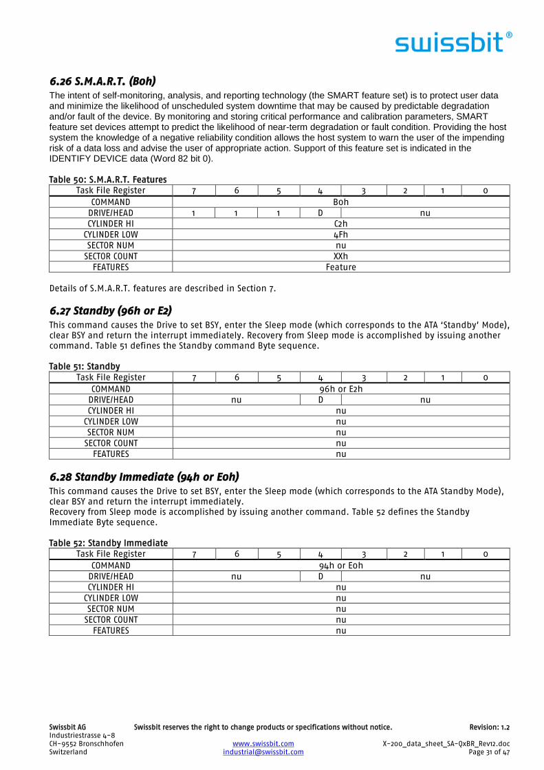
Swissbit AG Swissbit reserves the right to change products or specifications without notice. Revision: 1.2 Industriestrasse 4-8
CH-9552 Bronschhofen www.swissbit.com X-200_data_sheet_SA-QxBR_Rev12.doc Switzerland [email protected] Page 31 of 47
6.26 S.M.A.R.T. (B0h) The intent of self-monitoring, analysis, and reporting technology (the SMART feature set) is to protect user data and minimize the likelihood of unscheduled system downtime that may be caused by predictable degradation and/or fault of the device. By monitoring and storing critical performance and calibration parameters, SMART feature set devices attempt to predict the likelihood of near-term degradation or fault condition. Providing the host system the knowledge of a negative reliability condition allows the host system to warn the user of the impending risk of a data loss and advise the user of appropriate action. Support of this feature set is indicated in the IDENTIFY DEVICE data (Word 82 bit 0).
Table 50: S.M.A.R.T. Features
Task File Register 7 6 5 4 3 2 1 0
COMMAND B0h
DRIVE/HEAD 1 1 1 D nu
CYLINDER HI C2h
CYLINDER LOW 4Fh
SECTOR NUM nu
SECTOR COUNT XXh
FEATURES Feature
Details of S.M.A.R.T. features are described in Section 7.
6.27 Standby (96h or E2) This command causes the Drive to set BSY, enter the Sleep mode (which corresponds to the ATA ‘Standby’ Mode),
clear BSY and return the interrupt immediately. Recovery from Sleep mode is accomplished by issuing another
command. Table 51 defines the Standby command Byte sequence.
Table 51: Standby
Task File Register 7 6 5 4 3 2 1 0
COMMAND 96h or E2h
DRIVE/HEAD nu D nu
CYLINDER HI nu
CYLINDER LOW nu
SECTOR NUM nu
SECTOR COUNT nu
FEATURES nu
6.28 Standby Immediate (94h or E0h) This command causes the Drive to set BSY, enter the Sleep mode (which corresponds to the ATA Standby Mode),
clear BSY and return the interrupt immediately.
Recovery from Sleep mode is accomplished by issuing another command. Table 52 defines the Standby
Immediate Byte sequence.
Table 52: Standby Immediate
Task File Register 7 6 5 4 3 2 1 0
COMMAND 94h or E0h
DRIVE/HEAD nu D nu
CYLINDER HI nu
CYLINDER LOW nu
SECTOR NUM nu
SECTOR COUNT nu
FEATURES nu
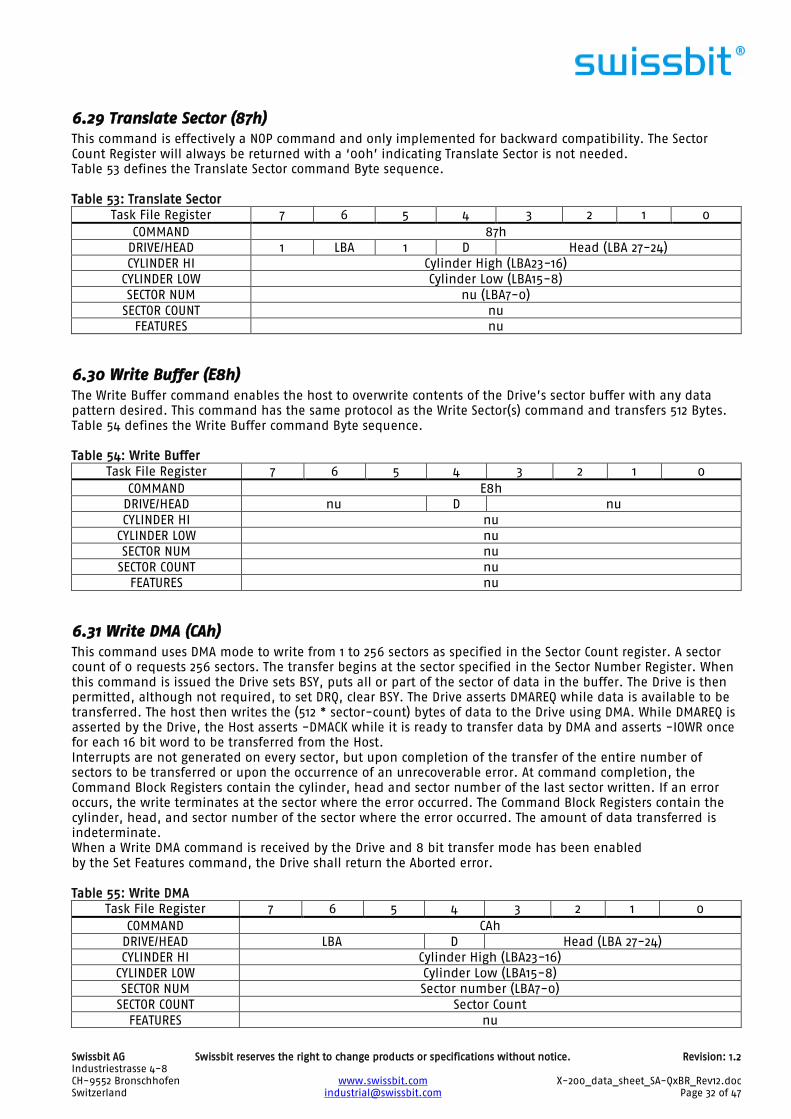
Swissbit AG Swissbit reserves the right to change products or specifications without notice. Revision: 1.2 Industriestrasse 4-8
CH-9552 Bronschhofen www.swissbit.com X-200_data_sheet_SA-QxBR_Rev12.doc Switzerland [email protected] Page 32 of 47
6.29 Translate Sector (87h) This command is effectively a NOP command and only implemented for backward compatibility. The Sector
Count Register will always be returned with a ‘00h’ indicating Translate Sector is not needed.
Table 53 defines the Translate Sector command Byte sequence.
Table 53: Translate Sector
Task File Register 7 6 5 4 3 2 1 0
COMMAND 87h
DRIVE/HEAD 1 LBA 1 D Head (LBA 27-24)
CYLINDER HI Cylinder High (LBA23-16)
CYLINDER LOW Cylinder Low (LBA15-8)
SECTOR NUM nu (LBA7-0)
SECTOR COUNT nu
FEATURES nu
6.30 Write Buffer (E8h) The Write Buffer command enables the host to overwrite contents of the Drive’s sector buffer with any data
pattern desired. This command has the same protocol as the Write Sector(s) command and transfers 512 Bytes.
Table 54 defines the Write Buffer command Byte sequence.
Table 54: Write Buffer
Task File Register 7 6 5 4 3 2 1 0
COMMAND E8h
DRIVE/HEAD nu D nu
CYLINDER HI nu
CYLINDER LOW nu
SECTOR NUM nu
SECTOR COUNT nu
FEATURES nu
6.31 Write DMA (CAh) This command uses DMA mode to write from 1 to 256 sectors as specified in the Sector Count register. A sector
count of 0 requests 256 sectors. The transfer begins at the sector specified in the Sector Number Register. When
this command is issued the Drive sets BSY, puts all or part of the sector of data in the buffer. The Drive is then
permitted, although not required, to set DRQ, clear BSY. The Drive asserts DMAREQ while data is available to be
transferred. The host then writes the (512 * sector-count) bytes of data to the Drive using DMA. While DMAREQ is
asserted by the Drive, the Host asserts -DMACK while it is ready to transfer data by DMA and asserts -IOWR once
for each 16 bit word to be transferred from the Host.
Interrupts are not generated on every sector, but upon completion of the transfer of the entire number of
sectors to be transferred or upon the occurrence of an unrecoverable error. At command completion, the
Command Block Registers contain the cylinder, head and sector number of the last sector written. If an error
occurs, the write terminates at the sector where the error occurred. The Command Block Registers contain the
cylinder, head, and sector number of the sector where the error occurred. The amount of data transferred is
indeterminate.
When a Write DMA command is received by the Drive and 8 bit transfer mode has been enabled
by the Set Features command, the Drive shall return the Aborted error.
Table 55: Write DMA
Task File Register 7 6 5 4 3 2 1 0
COMMAND CAh
DRIVE/HEAD LBA D Head (LBA 27-24)
CYLINDER HI Cylinder High (LBA23-16)
CYLINDER LOW Cylinder Low (LBA15-8)
SECTOR NUM Sector number (LBA7-0)
SECTOR COUNT Sector Count
FEATURES nu
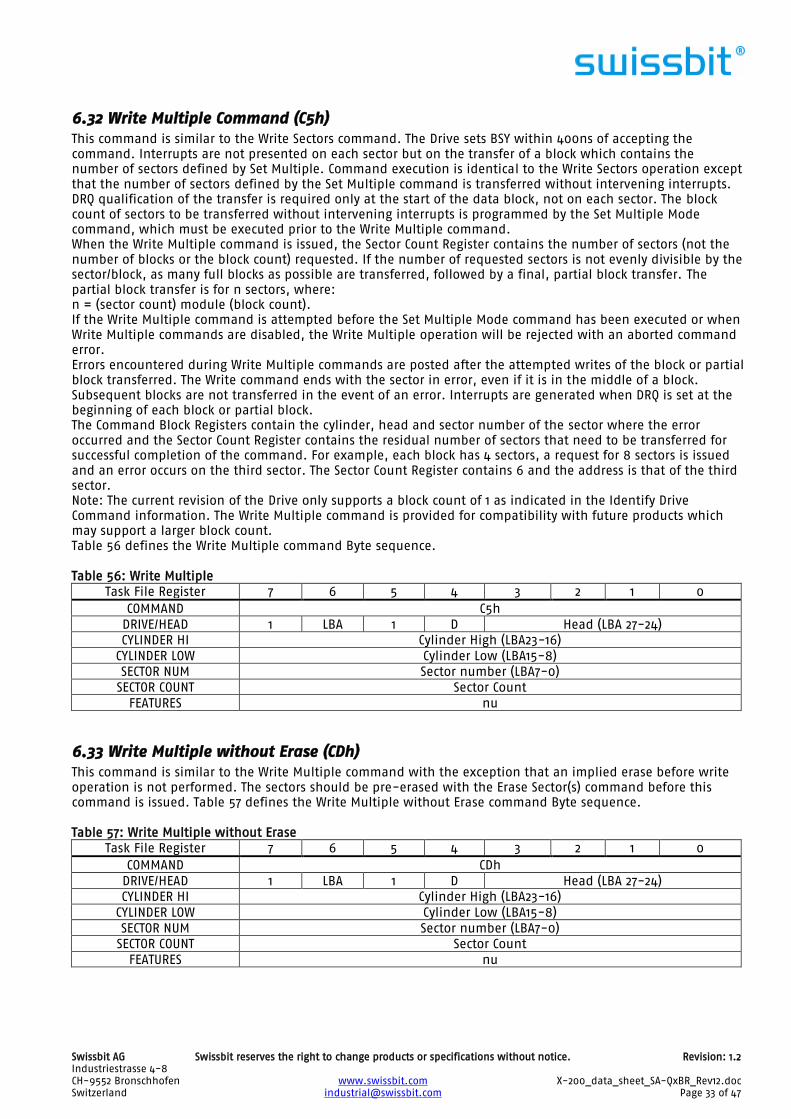
Swissbit AG Swissbit reserves the right to change products or specifications without notice. Revision: 1.2 Industriestrasse 4-8
CH-9552 Bronschhofen www.swissbit.com X-200_data_sheet_SA-QxBR_Rev12.doc Switzerland [email protected] Page 33 of 47
6.32 Write Multiple Command (C5h) This command is similar to the Write Sectors command. The Drive sets BSY within 400ns of accepting the
command. Interrupts are not presented on each sector but on the transfer of a block which contains the
number of sectors defined by Set Multiple. Command execution is identical to the Write Sectors operation except
that the number of sectors defined by the Set Multiple command is transferred without intervening interrupts.
DRQ qualification of the transfer is required only at the start of the data block, not on each sector. The block
count of sectors to be transferred without intervening interrupts is programmed by the Set Multiple Mode
command, which must be executed prior to the Write Multiple command.
When the Write Multiple command is issued, the Sector Count Register contains the number of sectors (not the
number of blocks or the block count) requested. If the number of requested sectors is not evenly divisible by the
sector/block, as many full blocks as possible are transferred, followed by a final, partial block transfer. The
partial block transfer is for n sectors, where:
n = (sector count) module (block count).
If the Write Multiple command is attempted before the Set Multiple Mode command has been executed or when
Write Multiple commands are disabled, the Write Multiple operation will be rejected with an aborted command
error.
Errors encountered during Write Multiple commands are posted after the attempted writes of the block or partial
block transferred. The Write command ends with the sector in error, even if it is in the middle of a block.
Subsequent blocks are not transferred in the event of an error. Interrupts are generated when DRQ is set at the
beginning of each block or partial block.
The Command Block Registers contain the cylinder, head and sector number of the sector where the error
occurred and the Sector Count Register contains the residual number of sectors that need to be transferred for
successful completion of the command. For example, each block has 4 sectors, a request for 8 sectors is issued
and an error occurs on the third sector. The Sector Count Register contains 6 and the address is that of the third
sector.
Note: The current revision of the Drive only supports a block count of 1 as indicated in the Identify Drive
Command information. The Write Multiple command is provided for compatibility with future products which
may support a larger block count.
Table 56 defines the Write Multiple command Byte sequence.
Table 56: Write Multiple
Task File Register 7 6 5 4 3 2 1 0
COMMAND C5h
DRIVE/HEAD 1 LBA 1 D Head (LBA 27-24)
CYLINDER HI Cylinder High (LBA23-16)
CYLINDER LOW Cylinder Low (LBA15-8)
SECTOR NUM Sector number (LBA7-0)
SECTOR COUNT Sector Count
FEATURES nu
6.33 Write Multiple without Erase (CDh) This command is similar to the Write Multiple command with the exception that an implied erase before write
operation is not performed. The sectors should be pre-erased with the Erase Sector(s) command before this
command is issued. Table 57 defines the Write Multiple without Erase command Byte sequence.
Table 57: Write Multiple without Erase
Task File Register 7 6 5 4 3 2 1 0
COMMAND CDh
DRIVE/HEAD 1 LBA 1 D Head (LBA 27-24)
CYLINDER HI Cylinder High (LBA23-16)
CYLINDER LOW Cylinder Low (LBA15-8)
SECTOR NUM Sector number (LBA7-0)
SECTOR COUNT Sector Count
FEATURES nu
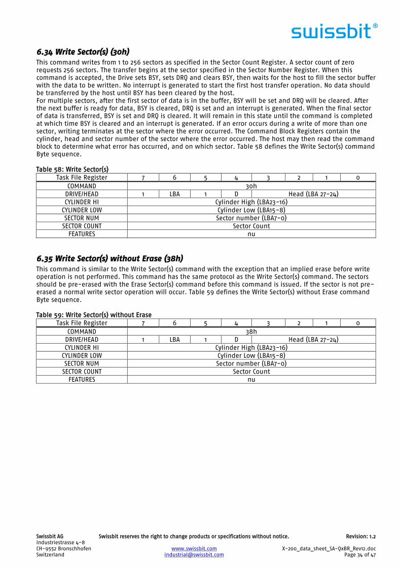
Swissbit AG Swissbit reserves the right to change products or specifications without notice. Revision: 1.2 Industriestrasse 4-8
CH-9552 Bronschhofen www.swissbit.com X-200_data_sheet_SA-QxBR_Rev12.doc Switzerland [email protected] Page 34 of 47
6.34 Write Sector(s) (30h) This command writes from 1 to 256 sectors as specified in the Sector Count Register. A sector count of zero
requests 256 sectors. The transfer begins at the sector specified in the Sector Number Register. When this
command is accepted, the Drive sets BSY, sets DRQ and clears BSY, then waits for the host to fill the sector buffer
with the data to be written. No interrupt is generated to start the first host transfer operation. No data should
be transferred by the host until BSY has been cleared by the host.
For multiple sectors, after the first sector of data is in the buffer, BSY will be set and DRQ will be cleared. After
the next buffer is ready for data, BSY is cleared, DRQ is set and an interrupt is generated. When the final sector
of data is transferred, BSY is set and DRQ is cleared. It will remain in this state until the command is completed
at which time BSY is cleared and an interrupt is generated. If an error occurs during a write of more than one
sector, writing terminates at the sector where the error occurred. The Command Block Registers contain the
cylinder, head and sector number of the sector where the error occurred. The host may then read the command
block to determine what error has occurred, and on which sector. Table 58 defines the Write Sector(s) command
Byte sequence.
Table 58: Write Sector(s)
Task File Register 7 6 5 4 3 2 1 0
COMMAND 30h
DRIVE/HEAD 1 LBA 1 D Head (LBA 27-24)
CYLINDER HI Cylinder High (LBA23-16)
CYLINDER LOW Cylinder Low (LBA15-8)
SECTOR NUM Sector number (LBA7-0)
SECTOR COUNT Sector Count
FEATURES nu
6.35 Write Sector(s) without Erase (38h) This command is similar to the Write Sector(s) command with the exception that an implied erase before write
operation is not performed. This command has the same protocol as the Write Sector(s) command. The sectors
should be pre-erased with the Erase Sector(s) command before this command is issued. If the sector is not pre-
erased a normal write sector operation will occur. Table 59 defines the Write Sector(s) without Erase command
Byte sequence.
Table 59: Write Sector(s) without Erase
Task File Register 7 6 5 4 3 2 1 0
COMMAND 38h
DRIVE/HEAD 1 LBA 1 D Head (LBA 27-24)
CYLINDER HI Cylinder High (LBA23-16)
CYLINDER LOW Cylinder Low (LBA15-8)
SECTOR NUM Sector number (LBA7-0)
SECTOR COUNT Sector Count
FEATURES nu
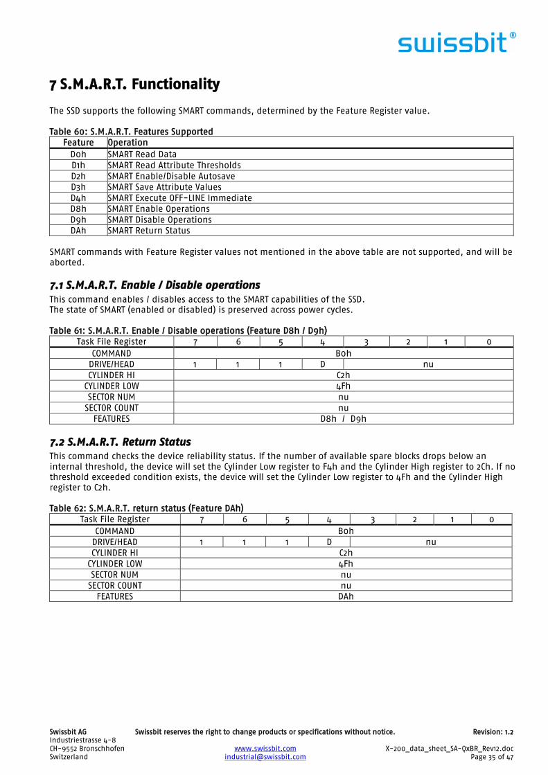
Swissbit AG Swissbit reserves the right to change products or specifications without notice. Revision: 1.2 Industriestrasse 4-8
CH-9552 Bronschhofen www.swissbit.com X-200_data_sheet_SA-QxBR_Rev12.doc Switzerland [email protected] Page 35 of 47
7 S.M.A.R.T. Functionality
The SSD supports the following SMART commands, determined by the Feature Register value.
Table 60: S.M.A.R.T. Features Supported
Feature Operation
D0h SMART Read Data
D1h SMART Read Attribute Thresholds
D2h SMART Enable/Disable Autosave
D3h SMART Save Attribute Values
D4h SMART Execute OFF-LINE Immediate
D8h SMART Enable Operations
D9h SMART Disable Operations
DAh SMART Return Status
SMART commands with Feature Register values not mentioned in the above table are not supported, and will be
aborted.
7.1 S.M.A.R.T. Enable / Disable operations This command enables / disables access to the SMART capabilities of the SSD.
The state of SMART (enabled or disabled) is preserved across power cycles.
Table 61: S.M.A.R.T. Enable / Disable operations (Feature D8h / D9h)
Task File Register 7 6 5 4 3 2 1 0
COMMAND B0h
DRIVE/HEAD 1 1 1 D nu
CYLINDER HI C2h
CYLINDER LOW 4Fh
SECTOR NUM nu
SECTOR COUNT nu
FEATURES D8h / D9h
7.2 S.M.A.R.T. Return Status This command checks the device reliability status. If the number of available spare blocks drops below an
internal threshold, the device will set the Cylinder Low register to F4h and the Cylinder High register to 2Ch. If no
threshold exceeded condition exists, the device will set the Cylinder Low register to 4Fh and the Cylinder High
register to C2h.
Table 62: S.M.A.R.T. return status (Feature DAh)
Task File Register 7 6 5 4 3 2 1 0
COMMAND B0h
DRIVE/HEAD 1 1 1 D nu
CYLINDER HI C2h
CYLINDER LOW 4Fh
SECTOR NUM nu
SECTOR COUNT nu
FEATURES DAh
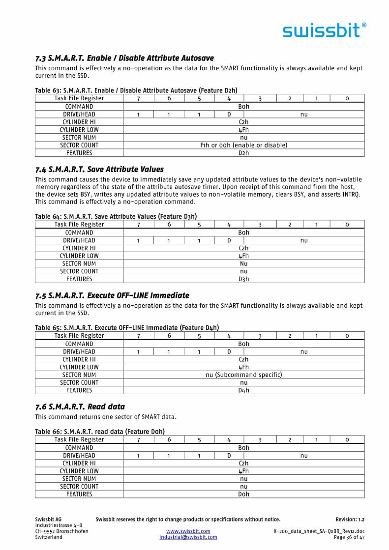
Swissbit AG Swissbit reserves the right to change products or specifications without notice. Revision: 1.2 Industriestrasse 4-8
CH-9552 Bronschhofen www.swissbit.com X-200_data_sheet_SA-QxBR_Rev12.doc Switzerland [email protected] Page 36 of 47
7.3 S.M.A.R.T. Enable / Disable Attribute Autosave This command is effectively a no-operation as the data for the SMART functionality is always available and kept
current in the SSD.
Table 63: S.M.A.R.T. Enable / Disable Attribute Autosave (Feature D2h)
Task File Register 7 6 5 4 3 2 1 0
COMMAND B0h
DRIVE/HEAD 1 1 1 D nu
CYLINDER HI C2h
CYLINDER LOW 4Fh
SECTOR NUM nu
SECTOR COUNT F1h or 00h (enable or disable)
FEATURES D2h
7.4 S.M.A.R.T. Save Attribute Values This command causes the device to immediately save any updated attribute values to the device’s non-volatile
memory regardless of the state of the attribute autosave timer. Upon receipt of this command from the host,
the device sets BSY, writes any updated attribute values to non-volatile memory, clears BSY, and asserts INTRQ.
This command is effectively a no-operation command.
Table 64: S.M.A.R.T. Save Attribute Values (Feature D3h)
Task File Register 7 6 5 4 3 2 1 0
COMMAND B0h
DRIVE/HEAD 1 1 1 D nu
CYLINDER HI C2h
CYLINDER LOW 4Fh
SECTOR NUM Nu
SECTOR COUNT nu
FEATURES D3h
7.5 S.M.A.R.T. Execute OFF-LINE Immediate This command is effectively a no-operation as the data for the SMART functionality is always available and kept
current in the SSD.
Table 65: S.M.A.R.T. Execute OFF-LINE Immediate (Feature D4h)
Task File Register 7 6 5 4 3 2 1 0
COMMAND B0h
DRIVE/HEAD 1 1 1 D nu
CYLINDER HI C2h
CYLINDER LOW 4Fh
SECTOR NUM nu (Subcommand specific)
SECTOR COUNT nu
FEATURES D4h
7.6 S.M.A.R.T. Read data This command returns one sector of SMART data.
Table 66: S.M.A.R.T. read data (Feature D0h)
Task File Register 7 6 5 4 3 2 1 0
COMMAND B0h
DRIVE/HEAD 1 1 1 D nu
CYLINDER HI C2h
CYLINDER LOW 4Fh
SECTOR NUM nu
SECTOR COUNT nu
FEATURES D0h
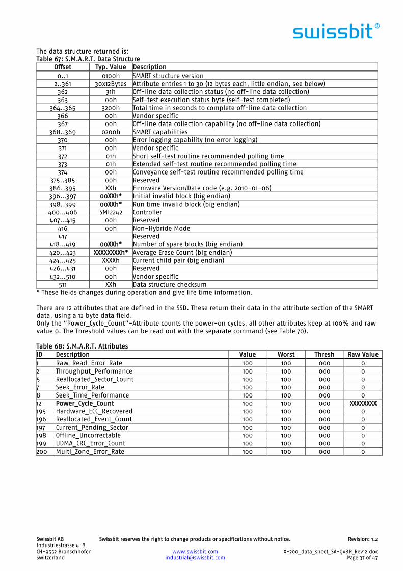
Swissbit AG Swissbit reserves the right to change products or specifications without notice. Revision: 1.2 Industriestrasse 4-8
CH-9552 Bronschhofen www.swissbit.com X-200_data_sheet_SA-QxBR_Rev12.doc Switzerland [email protected] Page 37 of 47
The data structure returned is:
Table 67: S.M.A.R.T. Data Structure
Offset Typ. Value Description
0..1 0100h SMART structure version
2..361 30x12Bytes Attribute entries 1 to 30 (12 bytes each, little endian, see below)
362 31h Off-line data collection status (no off-line data collection)
363 00h Self-test execution status byte (self-test completed)
364..365 3200h Total time in seconds to complete off-line data collection
366 00h Vendor specific
367 00h Off-line data collection capability (no off-line data collection)
368..369 0200h SMART capabilities
370 00h Error logging capability (no error logging)
371 00h Vendor specific
372 01h Short self-test routine recommended polling time
373 01h Extended self-test routine recommended polling time
374 00h Conveyance self-test routine recommended polling time
375..385 00h Reserved
386..395 XXh Firmware Version/Date code (e.g. 2010-01-06)
396…397 00XXh* Initial invalid block (big endian)
398..399 00XXh* Run time invalid block (big endian)
400…406 SMI2242 Controller
407…415 00h Reserved
416 00h Non-Hybride Mode
417 Reserved
418…419 00XXh* Number of spare blocks (big endian)
420…423 XXXXXXXXh* Average Erase Count (big endian)
424…425 XXXXh Current child pair (big endian)
426…431 00h Reserved
432…510 00h Vendor specific
511 XXh Data structure checksum
* These fields changes during operation and give life time information.
There are 12 attributes that are defined in the SSD. These return their data in the attribute section of the SMART
data, using a 12 byte data field.
Only the “Power_Cycle_Count”-Attribute counts the power-on cycles, all other attributes keep at 100% and raw
value 0. The Threshold values can be read out with the separate command (see Table 70).
Table 68: S.M.A.R.T. Attributes
ID Description Value Worst Thresh Raw Value
1 Raw_Read_Error_Rate 100 100 000 0
2 Throughput_Performance 100 100 000 0
5 Reallocated_Sector_Count 100 100 000 0
7 Seek_Error_Rate 100 100 000 0
8 Seek_Time_Performance 100 100 000 0
12 Power_Cycle_Count 100 100 000 XXXXXXXX
195 Hardware_ECC_Recovered 100 100 000 0
196 Reallocated_Event_Count 100 100 000 0
197 Current_Pending_Sector 100 100 000 0
198 Offline_Uncorrectable 100 100 000 0
199 UDMA_CRC_Error_Count 100 100 000 0
200 Multi_Zone_Error_Rate 100 100 000 0
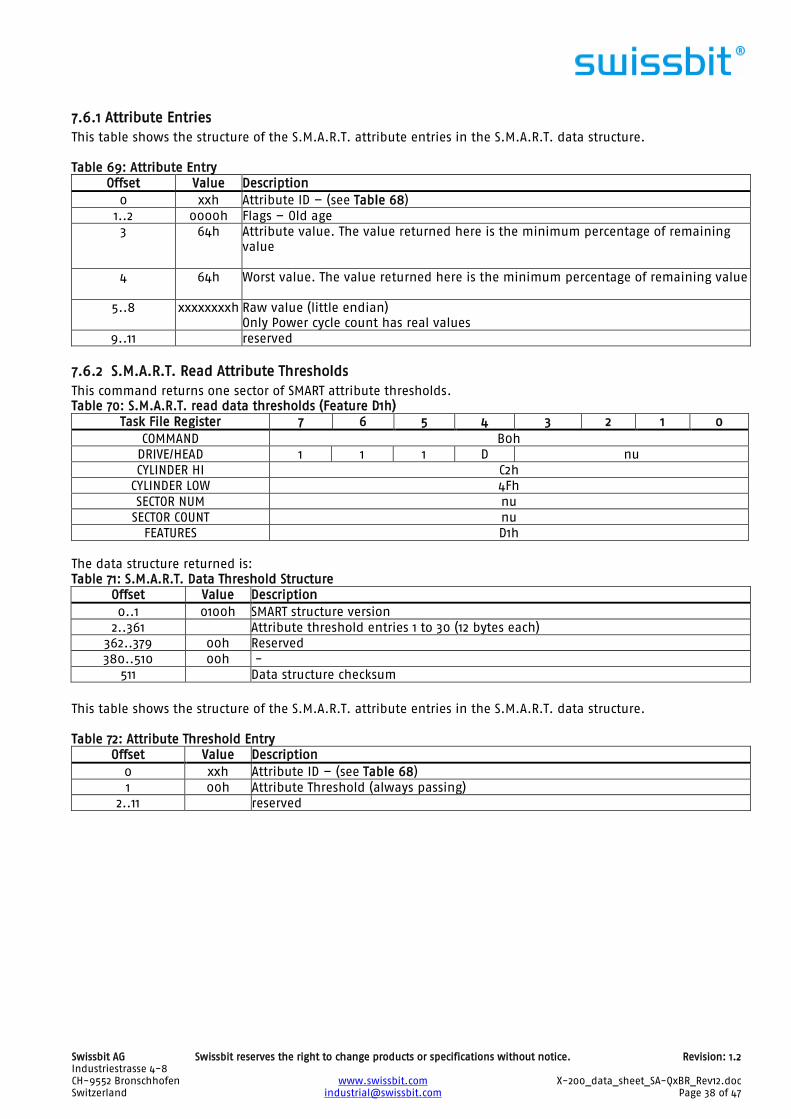
Swissbit AG Swissbit reserves the right to change products or specifications without notice. Revision: 1.2 Industriestrasse 4-8
CH-9552 Bronschhofen www.swissbit.com X-200_data_sheet_SA-QxBR_Rev12.doc Switzerland [email protected] Page 38 of 47
7.6.1 Attribute Entries
This table shows the structure of the S.M.A.R.T. attribute entries in the S.M.A.R.T. data structure.
Table 69: Attribute Entry
Offset Value Description
0 xxh Attribute ID – (see Table 68)
1..2 0000h Flags – Old age
3 64h Attribute value. The value returned here is the minimum percentage of remaining
value
4 64h Worst value. The value returned here is the minimum percentage of remaining value
5..8 xxxxxxxxh Raw value (little endian)
Only Power cycle count has real values
9..11 reserved
7.6.2 S.M.A.R.T. Read Attribute Thresholds
This command returns one sector of SMART attribute thresholds.
Table 70: S.M.A.R.T. read data thresholds (Feature D1h)
Task File Register 7 6 5 4 3 2 1 0
COMMAND B0h
DRIVE/HEAD 1 1 1 D nu
CYLINDER HI C2h
CYLINDER LOW 4Fh
SECTOR NUM nu
SECTOR COUNT nu
FEATURES D1h
The data structure returned is:
Table 71: S.M.A.R.T. Data Threshold Structure
Offset Value Description
0..1 0100h SMART structure version
2..361 Attribute threshold entries 1 to 30 (12 bytes each)
362..379 00h Reserved
380..510 00h -
511 Data structure checksum
This table shows the structure of the S.M.A.R.T. attribute entries in the S.M.A.R.T. data structure.
Table 72: Attribute Threshold Entry
Offset Value Description
0 xxh Attribute ID – (see Table 68)
1 00h Attribute Threshold (always passing)
2..11 reserved
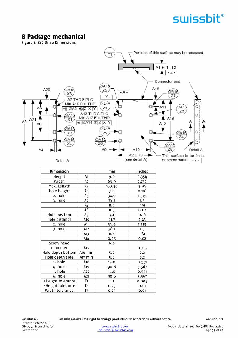
Swissbit AG Swissbit reserves the right to change products or specifications without notice. Revision: 1.2 Industriestrasse 4-8
CH-9552 Bronschhofen www.swissbit.com X-200_data_sheet_SA-QxBR_Rev12.doc Switzerland [email protected] Page 39 of 47
8 Package mechanical Figure 1: SSD Drive Dimensions
Dimension mm inches
Height A1 9.0 0.354
Width A2 69.9 2.752
Max. Length A3 100.30 3.94
Hole height A4 3.0 0.118
2. hole A5 34.9 1.375
3. hole A6 38.1 1.5
A7 n/a n/a
A8 0.5 0.02
Hole position A9 4.1 0.16
Hole distance A10 61.7 2.43
2. hole A11 34.9 1.375
3. hole A12 38.1 1.5
A13 n/a n/a
A14 0.05 0.02
Screw head
diameter A15
6.0
0.315
Hole depth bottom A16 min 5.0 0.2
Hole depth side A17 min 5.0 0.2
1. hole A18 14.0 0.551
4. hole A19 90.6 3.567
1. hole A20 14.0 0.551
4. hole A21 90.6 3.567
+Height tolerance T1 0.1 0.005
-Height tolerance T2 0.25 0.01
Width tolerance T3 0.25 0.01
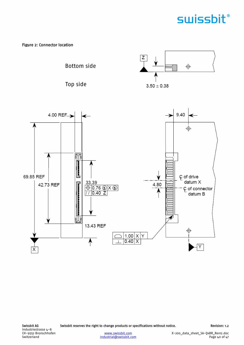
Swissbit AG Swissbit reserves the right to change products or specifications without notice. Revision: 1.2 Industriestrasse 4-8
CH-9552 Bronschhofen www.swissbit.com X-200_data_sheet_SA-QxBR_Rev12.doc Switzerland [email protected] Page 40 of 47
Figure 2: Connector location
Bottom side
Top side
Swissbit AG Swissbit reserves the right to change products or specifications without notice. Revision: 1.2 Industriestrasse 4-8
CH-9552 Bronschhofen www.swissbit.com X-200_data_sheet_SA-QxBR_Rev12.doc Switzerland [email protected] Page 41 of 47
9 Declaration of Conformity
Product Type: Solid State Drive (SSD)
Brand Name: SWISSMEMORYTM SSD
Model Designation: SFSAxxxxQxxxxxx-x-xx-xxx-xxx
Manufacturer: Swissbit AG
Industriestrasse 4
CH-9552 Bronschhofen
Switzerland
The product complies with the requirements of the following directives:
CENELEC EN 55022B :2000 + CISPR22B :2000
CENELEC EN 55024 :2001 + CISPR24 :2001
FCC47 Part 15 Subpart B
The product was tested according all EMC requirements necessary for -mark
Year of the first marking: 2010
Silvio Muschter
Vice President
Engineering & Development
Bronschhofen, August 2010
Swissbit AG Swissbit reserves the right to change products or specifications without notice. Revision: 1.2 Industriestrasse 4-8
CH-9552 Bronschhofen www.swissbit.com X-200_data_sheet_SA-QxBR_Rev12.doc Switzerland [email protected] Page 42 of 47
10 RoHS and WEEE update from Swissbit Dear Valued Customer,
We at Swissbit place great value on the environment and thus pay close attention to the diverse aspects of
manufacturing environmentally and health friendly products. The European Parliament and the Council of the
European Union have published two Directives defining a European standard for environmental protection. This
states that Solid State Drives must comply with both Directives in order for them to be sold on the European
market:
RoHS – Restriction of Hazardous Substances
WEEE – Waste Electrical and Electronic Equipment
Swissbit would like to take this opportunity to inform our customers about the measures we have implemented
to adapt all our products to the European norms.
What is the WEEE Directive (2002/96/EC)?
The Directive covers the following points:
Prevention of WEEE
Recovery, recycling and other measures leading to a minimization of wastage of electronic and
electrical equipment
Improvement in the quality of environmental performance of all operators involved in the EEE
life cycle, as well as measures to incorporate those involved at the EEE waste disposal points
What are the key elements?
The WEEE Directive covers the following responsibilities on the part of producers:
Producers must draft a disposal or recovery scheme to dispose of EEE correctly.
Producers must be registered as producers in the country in which they distribute the goods.
They must also supply and publish information about the EEE categories.
Producers are obliged to finance the collection, treatment and disposal of WEEE.
Inclusion of WEEE logos on devices
In reference to the Directive, the WEEE logo must be printed directly on all devices that have sufficient space.
«In exceptional cases where this is necessary because of the size of the product, the symbol of the WEEE
Directive shall be printed on the packaging, on the instructions of use and on the warranty»
(WEEE Directive 2002/96/EC)
When does the WEEE Directive take effect?
The Directive came into effect internationally on 13 August, 2005.
What is RoHS (2002/95/EC)?
The goals of the Directive are to:
Place less of a burden on human health and to protect the environment by restricting the use of
hazardous substances in new electrical and electronic devices
To support the WEEE Directive (see above)
RoHS enforces the restriction of the following 6 hazardous substances in electronic and electrical devices:
Lead (Pb) – no more than 0.1% by weight in homogeneous materials
Mercury (Hg) – no more than 0.1% by weight in homogeneous materials
Cadmium (Cd) – no more than 0.01% by weight in homogeneous materials
Chromium (Cr6+) – no more than 0.1% by weight in homogeneous materials
PBB, PBDE – no more than 0.1% by weight in homogeneous materials
Swissbit AG Swissbit reserves the right to change products or specifications without notice. Revision: 1.2 Industriestrasse 4-8
CH-9552 Bronschhofen www.swissbit.com X-200_data_sheet_SA-QxBR_Rev12.doc Switzerland [email protected] Page 43 of 47
Swissbit is obliged to minimize the hazardous substances in the products.
According to part of the Directive, manufacturers are obliged to make a self-declaration for all devices with
RoHS. Swissbit carried out intensive tests to comply with the self-declaration. We have also already taken steps
to have the analyses of the individual components guaranteed by third-party companies.
Swissbit carried out the following steps during the year with the goal of offering our customers products that are
fully compliant with the RoHS Directive.
Preparing all far-reaching directives, logistical enhancements and alternatives regarding the full
understanding and introduction of the RoHS Directive’s standards
Checking the components and raw materials:
o Replacing non-RoHS-compliant components and raw materials in the supply chain
o Cooperating closely with suppliers regarding the certification of all components and raw
materials used by Swissbit
Modifying the manufacturing processes and procedures
o Successfully adapting and optimizing the new management-free integration process in
the supply chain
o Updating existing production procedures and introducing the new procedures to support
the integration process and the sorting of materials
Carrying out the quality process
o Performing detailed function and safety tests to ensure the continuous high quality of
the Swissbit product line
When does the RoHS Directive take effect?
As of 1 July, 2006, only new electrical and electronic devices with approved quantities of RoHS will be put on the
market.
When will Swissbit be offering RoHS-approved products?
Swissbit’s RoHS-approved products are available now. Please contact your Swissbit contact person to find out
more about exchanging your existing products for RoHS-compliant devices.
For your attention
We understand that packaging and accessories are not EEE material and are therefore not subject to the WEEE or
RoHS Directives.
Contact details:
Swissbit AG
Industriestrasse 4
CH-9552 Bronschhofen
Tel: +41 71 913 03 03 – Fax: +41 71 913 03 15
E-mail: [email protected] – Website: www.swissbit.com
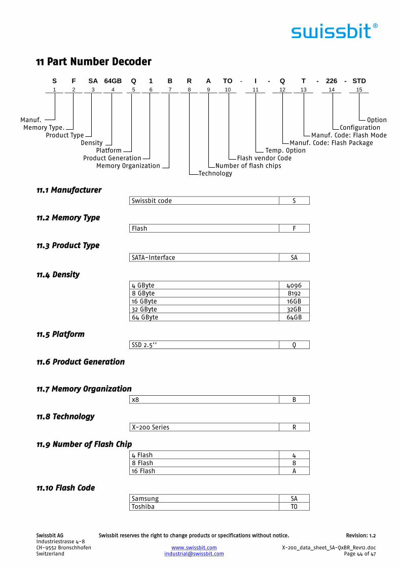
Swissbit AG Swissbit reserves the right to change products or specifications without notice. Revision: 1.2 Industriestrasse 4-8
CH-9552 Bronschhofen www.swissbit.com X-200_data_sheet_SA-QxBR_Rev12.doc Switzerland [email protected] Page 44 of 47
11 Part Number Decoder
S F SA 64GB Q 1 B R A TO - I - Q T - 226 - STD
1 2 3 4 5 6 7 8 9 10 11 12 13 14 15
Manuf. Option
Memory Type. Configuration
Product Type Manuf. Code: Flash Mode
Density Manuf. Code: Flash Package
Platform Temp. Option
Product Generation Flash vendor Code
Memory Organization Number of flash chips
Technology
11.1 Manufacturer
Swissbit code S
11.2 Memory Type
Flash F
11.3 Product Type
SATA-Interface SA
11.4 Density
4 GByte 4096
8 GByte 8192
16 GByte 16GB
32 GByte 32GB
64 GByte 64GB
11.5 Platform
SSD 2.5’’ Q
11.6 Product Generation
11.7 Memory Organization
x8 B
11.8 Technology
X-200 Series R
11.9 Number of Flash Chip
4 Flash 4
8 Flash 8
16 Flash A
11.10 Flash Code
Samsung SA
Toshiba TO
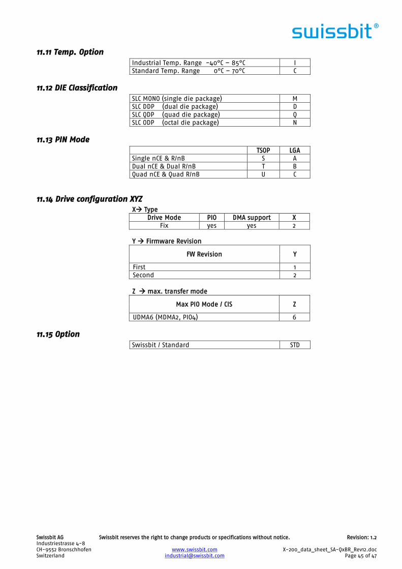
Swissbit AG Swissbit reserves the right to change products or specifications without notice. Revision: 1.2 Industriestrasse 4-8
CH-9552 Bronschhofen www.swissbit.com X-200_data_sheet_SA-QxBR_Rev12.doc Switzerland [email protected] Page 45 of 47
11.11 Temp. Option
Industrial Temp. Range -40°C – 85°C I
Standard Temp. Range 0°C – 70°C C
11.12 DIE Classification
SLC MONO (single die package) M
SLC DDP (dual die package) D
SLC QDP (quad die package) Q
SLC ODP (octal die package) N
11.13 PIN Mode
TSOP LGA
Single nCE & R/nB S A
Dual nCE & Dual R/nB T B
Quad nCE & Quad R/nB U C
11.14 Drive configuration XYZ X Type
Drive Mode PIO DMA support X
Fix yes yes 2
Y Firmware Revision
FW Revision Y
First 1
Second 2
Z max. transfer mode
Max PIO Mode / CIS Z
UDMA6 (MDMA2, PIO4) 6
11.15 Option
Swissbit / Standard STD
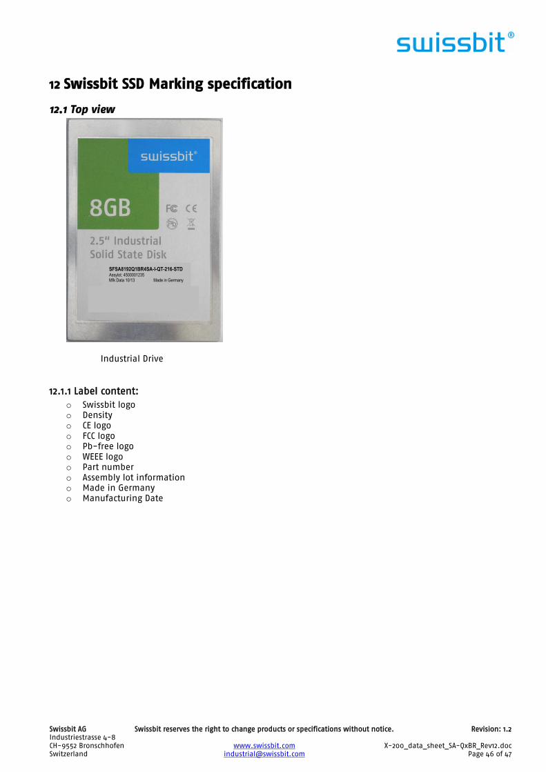
Swissbit AG Swissbit reserves the right to change products or specifications without notice. Revision: 1.2 Industriestrasse 4-8
CH-9552 Bronschhofen www.swissbit.com X-200_data_sheet_SA-QxBR_Rev12.doc Switzerland [email protected] Page 46 of 47
12 Swissbit SSD Marking specification
12.1 Top view
Industrial Drive
12.1.1 Label content:
o Swissbit logo
o Density
o CE logo
o FCC logo
o Pb-free logo
o WEEE logo
o Part number
o Assembly lot information
o Made in Germany
o Manufacturing Date
SFSA8192Q1BR4SA-I-QT-216-STD
Assylot: 4500001235 Mfk Data 10/13 Made in Germany
Swissbit AG Swissbit reserves the right to change products or specifications without notice. Revision: 1.2 Industriestrasse 4-8
CH-9552 Bronschhofen www.swissbit.com X-200_data_sheet_SA-QxBR_Rev12.doc Switzerland [email protected] Page 47 of 47
13 Revision History
Table 73: Document Revision History Date Revision Revision Details
29-September-2010 1.00 Initial release
17-August-2011 1.10 Small performance correction, S.M.A.R.T. added to feature list
31-October-2011 1.11 32GB and 64GB speed modified
02-January-2012 1.2 different LBA density for 64GB Firmware “2”
Disclaimer:
No part of this document may be copied or reproduced in any form or by any means, or transferred to any third
party, without the prior written consent of an authorized representative of Swissbit AG (“SWISSBIT”). The
information in this document is subject to change without notice. SWISSBIT assumes no responsibility for any
errors or omissions that may appear in this document, and disclaims responsibility for any consequences
resulting from the use of the information set forth herein. SWISSBIT makes no commitments to update or to keep
current information contained in this document. The products listed in this document are not suitable for use in
applications such as, but not limited to, aircraft control systems, aerospace equipment, submarine cables,
nuclear reactor control systems and life support systems. Moreover, SWISSBIT does not recommend or approve
the use of any of its products in life support devices or systems or in any application where failure could result
in injury or death. If a customer wishes to use SWISSBIT products in applications not intended by SWISSBIT, said
customer must contact an authorized SWISSBIT representative to determine SWISSBIT willingness to support a
given application. The information set forth in this document does not convey any license under the copyrights,
patent rights, trademarks or other intellectual property rights claimed and owned by SWISSBIT. The information
set forth in this document is considered to be “Proprietary” and “Confidential” property owned by SWISSBIT.
ALL PRODUCTS SOLD BY SWISSBIT ARE COVERED BY THE PROVISIONS APPEARING IN SWISSBIT’S TERMS AND CONDITIONS OF
SALE ONLY, INCLUDING THE LIMITATIONS OF LIABILITY, WARRANTY AND INFRINGEMENT PROVISIONS. SWISSBIT MAKES NO
WARRANTIES OF ANY KIND, EXPRESS, STATUTORY, IMPLIED OR OTHERWISE, REGARDING INFORMATION SET FORTH HEREIN
OR REGARDING THE FREEDOM OF THE DESCRIBED PRODUCTS FROM INTELLECTUAL PROPERTY INFRINGEMENT, AND
EXPRESSLY DISCLAIMS ANY SUCH WARRANTIES INCLUDING WITHOUT LIMITATION ANY EXPRESS, STATUTORY OR IMPLIED
WARRANTIES OF MERCHANTABILITY OR FITNESS FOR A PARTICULAR PURPOSE.
©2012 SWISSBIT AG All rights reserved.